WO2018008281A1 - 蛍光体および発光装置 - Google Patents
蛍光体および発光装置 Download PDFInfo
- Publication number
- WO2018008281A1 WO2018008281A1 PCT/JP2017/019464 JP2017019464W WO2018008281A1 WO 2018008281 A1 WO2018008281 A1 WO 2018008281A1 JP 2017019464 W JP2017019464 W JP 2017019464W WO 2018008281 A1 WO2018008281 A1 WO 2018008281A1
- Authority
- WO
- WIPO (PCT)
- Prior art keywords
- phosphor
- light
- wavelength
- emitting device
- excitation
- Prior art date
Links
Images


Classifications
-
- C—CHEMISTRY; METALLURGY
- C09—DYES; PAINTS; POLISHES; NATURAL RESINS; ADHESIVES; COMPOSITIONS NOT OTHERWISE PROVIDED FOR; APPLICATIONS OF MATERIALS NOT OTHERWISE PROVIDED FOR
- C09K—MATERIALS FOR MISCELLANEOUS APPLICATIONS, NOT PROVIDED FOR ELSEWHERE
- C09K11/00—Luminescent, e.g. electroluminescent, chemiluminescent materials
- C09K11/08—Luminescent, e.g. electroluminescent, chemiluminescent materials containing inorganic luminescent materials
- C09K11/77—Luminescent, e.g. electroluminescent, chemiluminescent materials containing inorganic luminescent materials containing rare earth metals
- C09K11/7766—Luminescent, e.g. electroluminescent, chemiluminescent materials containing inorganic luminescent materials containing rare earth metals containing two or more rare earth metals
- C09K11/77747—Silicon Nitrides or Silicon Oxynitrides
-
- C—CHEMISTRY; METALLURGY
- C09—DYES; PAINTS; POLISHES; NATURAL RESINS; ADHESIVES; COMPOSITIONS NOT OTHERWISE PROVIDED FOR; APPLICATIONS OF MATERIALS NOT OTHERWISE PROVIDED FOR
- C09K—MATERIALS FOR MISCELLANEOUS APPLICATIONS, NOT PROVIDED FOR ELSEWHERE
- C09K11/00—Luminescent, e.g. electroluminescent, chemiluminescent materials
- C09K11/08—Luminescent, e.g. electroluminescent, chemiluminescent materials containing inorganic luminescent materials
- C09K11/77—Luminescent, e.g. electroluminescent, chemiluminescent materials containing inorganic luminescent materials containing rare earth metals
- C09K11/7715—Luminescent, e.g. electroluminescent, chemiluminescent materials containing inorganic luminescent materials containing rare earth metals containing cerium
- C09K11/77217—Silicon Nitrides or Silicon Oxynitrides
-
- F—MECHANICAL ENGINEERING; LIGHTING; HEATING; WEAPONS; BLASTING
- F21—LIGHTING
- F21K—NON-ELECTRIC LIGHT SOURCES USING LUMINESCENCE; LIGHT SOURCES USING ELECTROCHEMILUMINESCENCE; LIGHT SOURCES USING CHARGES OF COMBUSTIBLE MATERIAL; LIGHT SOURCES USING SEMICONDUCTOR DEVICES AS LIGHT-GENERATING ELEMENTS; LIGHT SOURCES NOT OTHERWISE PROVIDED FOR
- F21K9/00—Light sources using semiconductor devices as light-generating elements, e.g. using light-emitting diodes [LED] or lasers
- F21K9/60—Optical arrangements integrated in the light source, e.g. for improving the colour rendering index or the light extraction
-
- F—MECHANICAL ENGINEERING; LIGHTING; HEATING; WEAPONS; BLASTING
- F21—LIGHTING
- F21V—FUNCTIONAL FEATURES OR DETAILS OF LIGHTING DEVICES OR SYSTEMS THEREOF; STRUCTURAL COMBINATIONS OF LIGHTING DEVICES WITH OTHER ARTICLES, NOT OTHERWISE PROVIDED FOR
- F21V9/00—Elements for modifying spectral properties, polarisation or intensity of the light emitted, e.g. filters
- F21V9/30—Elements containing photoluminescent material distinct from or spaced from the light source
-
- H—ELECTRICITY
- H01—ELECTRIC ELEMENTS
- H01S—DEVICES USING THE PROCESS OF LIGHT AMPLIFICATION BY STIMULATED EMISSION OF RADIATION [LASER] TO AMPLIFY OR GENERATE LIGHT; DEVICES USING STIMULATED EMISSION OF ELECTROMAGNETIC RADIATION IN WAVE RANGES OTHER THAN OPTICAL
- H01S5/00—Semiconductor lasers
- H01S5/005—Optical components external to the laser cavity, specially adapted therefor, e.g. for homogenisation or merging of the beams or for manipulating laser pulses, e.g. pulse shaping
- H01S5/0087—Optical components external to the laser cavity, specially adapted therefor, e.g. for homogenisation or merging of the beams or for manipulating laser pulses, e.g. pulse shaping for illuminating phosphorescent or fluorescent materials, e.g. using optical arrangements specifically adapted for guiding or shaping laser beams illuminating these materials
-
- H—ELECTRICITY
- H01—ELECTRIC ELEMENTS
- H01S—DEVICES USING THE PROCESS OF LIGHT AMPLIFICATION BY STIMULATED EMISSION OF RADIATION [LASER] TO AMPLIFY OR GENERATE LIGHT; DEVICES USING STIMULATED EMISSION OF ELECTROMAGNETIC RADIATION IN WAVE RANGES OTHER THAN OPTICAL
- H01S5/00—Semiconductor lasers
- H01S5/30—Structure or shape of the active region; Materials used for the active region
- H01S5/32—Structure or shape of the active region; Materials used for the active region comprising PN junctions, e.g. hetero- or double- heterostructures
- H01S5/323—Structure or shape of the active region; Materials used for the active region comprising PN junctions, e.g. hetero- or double- heterostructures in AIIIBV compounds, e.g. AlGaAs-laser, InP-based laser
- H01S5/32308—Structure or shape of the active region; Materials used for the active region comprising PN junctions, e.g. hetero- or double- heterostructures in AIIIBV compounds, e.g. AlGaAs-laser, InP-based laser emitting light at a wavelength less than 900 nm
- H01S5/32341—Structure or shape of the active region; Materials used for the active region comprising PN junctions, e.g. hetero- or double- heterostructures in AIIIBV compounds, e.g. AlGaAs-laser, InP-based laser emitting light at a wavelength less than 900 nm blue laser based on GaN or GaP
-
- F—MECHANICAL ENGINEERING; LIGHTING; HEATING; WEAPONS; BLASTING
- F21—LIGHTING
- F21Y—INDEXING SCHEME ASSOCIATED WITH SUBCLASSES F21K, F21L, F21S and F21V, RELATING TO THE FORM OR THE KIND OF THE LIGHT SOURCES OR OF THE COLOUR OF THE LIGHT EMITTED
- F21Y2113/00—Combination of light sources
- F21Y2113/10—Combination of light sources of different colours
- F21Y2113/13—Combination of light sources of different colours comprising an assembly of point-like light sources
- F21Y2113/17—Combination of light sources of different colours comprising an assembly of point-like light sources forming a single encapsulated light source
-
- F—MECHANICAL ENGINEERING; LIGHTING; HEATING; WEAPONS; BLASTING
- F21—LIGHTING
- F21Y—INDEXING SCHEME ASSOCIATED WITH SUBCLASSES F21K, F21L, F21S and F21V, RELATING TO THE FORM OR THE KIND OF THE LIGHT SOURCES OR OF THE COLOUR OF THE LIGHT EMITTED
- F21Y2115/00—Light-generating elements of semiconductor light sources
- F21Y2115/10—Light-emitting diodes [LED]
-
- H—ELECTRICITY
- H01—ELECTRIC ELEMENTS
- H01L—SEMICONDUCTOR DEVICES NOT COVERED BY CLASS H10
- H01L33/00—Semiconductor devices with at least one potential-jump barrier or surface barrier specially adapted for light emission; Processes or apparatus specially adapted for the manufacture or treatment thereof or of parts thereof; Details thereof
- H01L33/48—Semiconductor devices with at least one potential-jump barrier or surface barrier specially adapted for light emission; Processes or apparatus specially adapted for the manufacture or treatment thereof or of parts thereof; Details thereof characterised by the semiconductor body packages
- H01L33/50—Wavelength conversion elements
-
- H—ELECTRICITY
- H01—ELECTRIC ELEMENTS
- H01S—DEVICES USING THE PROCESS OF LIGHT AMPLIFICATION BY STIMULATED EMISSION OF RADIATION [LASER] TO AMPLIFY OR GENERATE LIGHT; DEVICES USING STIMULATED EMISSION OF ELECTROMAGNETIC RADIATION IN WAVE RANGES OTHER THAN OPTICAL
- H01S5/00—Semiconductor lasers
- H01S5/02—Structural details or components not essential to laser action
- H01S5/022—Mountings; Housings
- H01S5/02208—Mountings; Housings characterised by the shape of the housings
- H01S5/02212—Can-type, e.g. TO-CAN housings with emission along or parallel to symmetry axis
-
- Y—GENERAL TAGGING OF NEW TECHNOLOGICAL DEVELOPMENTS; GENERAL TAGGING OF CROSS-SECTIONAL TECHNOLOGIES SPANNING OVER SEVERAL SECTIONS OF THE IPC; TECHNICAL SUBJECTS COVERED BY FORMER USPC CROSS-REFERENCE ART COLLECTIONS [XRACs] AND DIGESTS
- Y02—TECHNOLOGIES OR APPLICATIONS FOR MITIGATION OR ADAPTATION AGAINST CLIMATE CHANGE
- Y02B—CLIMATE CHANGE MITIGATION TECHNOLOGIES RELATED TO BUILDINGS, e.g. HOUSING, HOUSE APPLIANCES OR RELATED END-USER APPLICATIONS
- Y02B20/00—Energy efficient lighting technologies, e.g. halogen lamps or gas discharge lamps
Definitions
- the present disclosure relates to a phosphor and a light emitting device.
- the current general white LED has a configuration in which a blue LED chip, which is a blue light emitting element, and a phosphor are combined.
- a blue LED chip which is a blue light emitting element
- a phosphor a part of the light from the blue LED chip is color-converted by the phosphor, and the blue light from the blue LED chip and the light emitted from the phosphor are mixed to produce white light.
- LD Laser Diode
- a white solid light source As a white solid light source, a combination of a blue LED chip or a blue LD and a yellow phosphor is currently mainstream. For the purpose of improving color rendering properties, color reproducibility, etc., or obtaining a white color having a low color temperature, a white light source that combines a red phosphor in addition to a blue light source and a yellow phosphor has been developed.
- Patent Document 1 the general formula Y 3 Al 5 O 12 : Ce 3+ (hereinafter abbreviated as YAG: Ce), or the general formula La 3 Si 6 N 11 : Ce 3+ (hereinafter abbreviated as LSN: Ce) shown in Patent Document 1.
- yellow phosphors having Ce as the emission center are known.
- a red phosphor having Eu as the emission center is known, as in the general formula (Sr, Ca) AlSiN 3 : Eu 2+ (hereinafter abbreviated as CASN: Eu) shown in Patent Document 2.
- the present disclosure provides a phosphor having an emission center of Ce.
- the phosphor in one embodiment of the present disclosure includes a crystal phase having the chemical composition Ce x Y y La 3-xy Si 6 N 11 , where 0 ⁇ x ⁇ 0.6, and (1.5-x ) ⁇ y ⁇ (3-x), having an emission spectrum peak in the wavelength range of 600 nm to 660 nm and having an excitation spectrum first peak in the wavelength range of 480 nm to 550 nm.
- the comprehensive or specific aspect of the present disclosure may be realized by a phosphor, an element, an apparatus, a system, a vehicle, a method, or any combination thereof.
- a phosphor having Ce as the emission center can be realized.
- FIG. 1A is a conceptual diagram showing the splitting of 4f and 5d orbits of rare earth ions.
- FIG. 1B is a conceptual diagram showing the splitting of the 4f and 5d orbits of Ce 3+ , Eu 2+ and Yb 2+ .
- FIG. 2 is an energy level diagram of Ce 3+ in vacuum and in a crystal.
- FIG. 3 is a coordination coordinate model diagram between the 4f trajectory and the 5d trajectory.
- FIG. 4 is a graph showing the relationship between the excitation wavelength and the emission wavelength for the (La, Y) 3 Si 6 N 11 : Ce phosphor.
- FIG. 6 shows the relationship between the average coordination distance r ave and the excitation wavelength ⁇ ex and the relationship between the average coordination distance r ave and the emission wavelength ⁇ em for the (La, Y) 3 Si 6 N 11 : Ce phosphor.
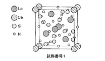
- FIG. 7 is a diagram showing a crystal structure of La 3 Si 6 N 11 and two types of sites of La.
- FIG. 8A is a diagram showing the crystal structure of sample number 1 for the (La, Y) 3 Si 6 N 11 : Ce phosphor.
- FIG. 8B is a diagram showing the crystal structure of sample number 2 for the (La, Y) 3 Si 6 N 11 : Ce phosphor.
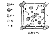
- FIG. 8C is a diagram showing the crystal structure of sample number 3 for the (La, Y) 3 Si 6 N 11 : Ce phosphor.
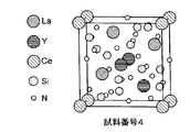
- FIG. 8D is a diagram showing the crystal structure of sample number 4 for the (La, Y) 3 Si 6 N 11 : Ce phosphor.
- FIG. 8E is a diagram showing the crystal structure of sample number 5 for the (La, Y) 3 Si 6 N 11 : Ce phosphor.
- FIG. 8B is a diagram showing the crystal structure of sample number 2 for the (La, Y) 3 Si 6 N 11 : Ce phosphor.
- FIG. 8C is a diagram showing the crystal structure of sample number 3 for the (La, Y) 3 Si
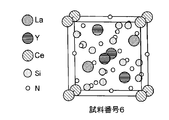
- FIG. 8F is a diagram showing the crystal structure of sample number 6 for the (La, Y) 3 Si 6 N 11 : Ce phosphor.
- FIG. 8G is a diagram showing the crystal structure of sample number 7 for the (La, Y) 3 Si 6 N 11 : Ce phosphor.
- FIG. 8H is a diagram showing the crystal structure of sample number 8 for the (La, Y) 3 Si 6 N 11 : Ce phosphor.
- FIG. 8I is a diagram showing the crystal structure of sample number 9 for the (La, Y) 3 Si 6 N 11 : Ce phosphor.
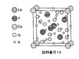
- FIG. 8J is a diagram showing the crystal structure of sample number 10 for the (La, Y) 3 Si 6 N 11 : Ce phosphor.
- FIG. 8G is a diagram showing the crystal structure of sample number 7 for the (La, Y) 3 Si 6 N 11 : Ce phosphor.
- FIG. 8H is a diagram showing the crystal structure of sample number 8 for the (La, Y) 3 Si
- FIG. 9 is a diagram showing powder XRD diffraction pattern results calculated from the crystal structure of the phosphors of sample numbers 1 to 10 shown in FIGS. 8A to 8J.
- FIG. 10 is a schematic cross-sectional view of the LED light emitting device according to the second embodiment.
- FIG. 11 is a schematic cross-sectional view of the LD light-emitting device according to the third embodiment.
- FIG. 12 is a schematic cross-sectional view of the LD light emitting device according to the fourth embodiment.
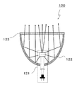
- FIG. 13 is a schematic cross-sectional view of the lighting apparatus according to the fifth embodiment.
- FIG. 14 is a schematic cross-sectional view of the lighting apparatus according to the sixth embodiment.
- FIG. 15 is a schematic cross-sectional view of a vehicle according to the seventh embodiment.
- the first is a pseudo-white light source that combines a blue LED and a yellow phosphor YAG: Ce.
- This type of light-emitting device is widely used because it can reduce power consumption and easily perform LED drive control.
- this white light source has only two color components, warm light such as a light bulb color cannot be produced, and color control is difficult.
- the second is a white light source that combines a blue LED, a yellow phosphor YAG: Ce, and a red phosphor CASN: Eu.
- white is a mixed color of three color components
- arbitrary white light can be produced by adjusting the light intensity of each color component. Therefore, this type of light-emitting device is easier to control the color than the above-described light-emitting device having two colors of color components.
- the yellow phosphor YAG: Ce used in this light-emitting device has a high quantum efficiency of light emission, and the quantum efficiency of light emission hardly changes even when excited by a high-power blue LED or blue LD.
- the red phosphor CASN Eu has a problem that the quantum efficiency of light emission is lowered when excited with high output light, and is mounted only on a relatively low output light source. This is because a phosphor having an emission center of Eu has a longer emission lifetime than a phosphor having an emission center of Ce, so that the luminance is easily saturated at the time of high output excitation. Therefore, conventionally, it has not been possible to realize a white light source with high output and easy color control.
- the phosphor according to the first aspect of the present disclosure includes a crystal phase having the chemical composition Ce x Y y La 3-xy Si 6 N 11 , and 0 ⁇ x ⁇ 0.6, (1. 5-x) ⁇ y ⁇ (3-x), and has an emission spectrum peak in a wavelength range of 600 nm to 660 nm and a first excitation spectrum peak in a wavelength range of 480 nm to 550 nm.
- a phosphor having Ce as the emission center can be realized.
- the x and the y of the phosphor according to the first aspect may satisfy (1.5 ⁇ 0.5x) ⁇ y ⁇ (3-x).
- the emission wavelength and the excitation wavelength can be increased.
- the x and y of the phosphor according to the second aspect may satisfy 1.5 ⁇ y ⁇ (3-x).
- the phosphor according to the third aspect it is possible to further increase the emission wavelength and the excitation wavelength.
- the crystal phase may have a tetragonal crystal structure.
- the phosphor according to at least one of the first to fourth aspects may have the second peak of the excitation spectrum within a wavelength range of 350 nm or more and less than 480 nm. .
- the phosphor according to the fifth aspect can emit light even with shorter wavelength excitation light such as 450 nm of blue LED and 405 nm of blue-violet LD, the choice of excitation light source is widened.
- the 1 / e emission lifetime of the crystal phase of the phosphor according to at least one of the first to fifth aspects may be 100 ns or less.
- the phosphor according to the sixth aspect is excellent in luminance saturation characteristics, it is promising as a red phosphor having high quantum efficiency even at high output.
- the crystal phase of the phosphor according to at least one of the first to sixth aspects is a La (2a) site in a crystal structure in which Ce is La 3 Si 6 N 11 . It may have a crystal structure that is at least partially substituted.
- the phosphor according to the seventh aspect is suitable for combination with, for example, a green excitation light source because it can emit light even with longer wavelength excitation light.
- the crystal phase of the phosphor according to at least one of the first to seventh aspects is a La (4c) site in a crystal structure in which Y is La 3 Si 6 N 11 . It may have a crystal structure that is at least partially substituted.
- the lattice constants of the a-axis and b-axis of the crystal lattice are The c-axis is relatively extended. For this reason, lattice distortion increases, and as a result, the energy difference between 4f-5d orbits decreases, and the emission wavelength can be lengthened.
- the crystal phase of the phosphor according to the eighth aspect has a crystal structure in which a majority of the La (4c) sites in the crystal structure where Y is La 3 Si 6 N 11 is substituted. You can do it.
- the crystal distortion rapidly increases, and as a result, the wavelength shift toward the long wavelength side increases rapidly, so that red light emission is possible.
- a light emitting device includes an excitation light source that emits light having a wavelength of 600 nm or less, and a first phosphor that is a phosphor according to at least one of the first to ninth aspects. .
- the first phosphor is irradiated with light emitted from the excitation light source and emits fluorescence having a longer wavelength than the light.
- the light-emitting device according to the tenth aspect includes the phosphor according to at least one of the first to ninth aspects, the quantum efficiency can be improved over the conventional light-emitting device at high output. Can do. Furthermore, when the light-emitting device according to the tenth aspect is configured as a white light-emitting device, high color rendering properties and color reproducibility can be realized.
- the excitation light source of the light emitting device according to the tenth aspect may emit light having a wavelength of 480 nm to 600 nm.
- the phosphor can be excited efficiently.
- the excitation light source of the light emitting device according to the tenth aspect may emit light having a wavelength of 420 nm or more and 480 nm or less.
- a GaN blue LED or blue LD can be used as an excitation light source.
- the excitation light source may be an LED or an LD.
- a high-output light emitting device can be realized.
- the light emitting device is irradiated with light emitted from the excitation light source, and emits fluorescence having a longer wavelength than the light.
- the second phosphor may have an emission spectrum peak in a wavelength range of 480 nm or more and less than 600 nm.
- the emission color can be controlled.
- the second phosphor is a phosphor that emits yellow light, is irradiated with light emitted from the excitation light source, and has a longer wavelength than the light.
- a third phosphor that emits the above fluorescence may be further provided, and the third phosphor may emit green light.
- the light emitting device of the fifteenth aspect includes at least two types of phosphors, that is, a phosphor that emits yellow light and a phosphor that emits green light, the emission color can be controlled.
- Embodiment 1 demonstrates embodiment of the fluorescent substance of this indication.
- embodiments of the phosphor of the present disclosure will be described including how the present inventors reached the phosphor of the present disclosure.
- rare earth elements Ce, Pr, Nd, Pm, Sm, Eu, Gd, Tb, Dy, Ho, Er, Tm, and Yb are in the state of divalent or trivalent ions and have valence electrons in the 4f orbit.
- the degeneracy of the 4f orbit is solved and the fragmentation is largely performed as conceptually shown in FIG. 1A.
- light emission can be obtained by utilizing a transition from one 4f level to another 4f level (ff transition). Since the ff transition is a forbidden transition, it has a feature that the lifetime of excited electrons is long. Therefore, a phosphor containing rare earth ions is often used as a laser medium. However, when such a phosphor is used as an incoherent light source such as general illumination, the light emission intensity is saturated immediately.
- Ce 3+ has only one electron in the 4f orbit as a valence electron.
- the split of the 4f orbit of Ce 3+ is extremely small compared to other rare earth ions.
- energy splitting of Eu 2+ and Yb 2+ 4f orbits is small. This is because Eu 2+ is a semi-closed shell with 7 electrons in the 4f orbit and Yb 2+ is a closed shell with 14 electrons in the 4f orbit.
- Ce 3+ , Eu 2+ and Yb 2+ have a small energy difference between the 4f ground level and the 5d orbital because the 4f orbit splitting is small. Further, there is no 4f orbit having a large energy between the 4f ground level and the 5d orbital. Therefore, it is easy to use the transition between 4f and 5d (4f-5d transition).
- the present inventors have further, Ce 3+, focused on Ce 3+ of Eu 2+ and Yb 2+. Since Ce 3+ has one electron involved in the 4f-5d transition, when it falls from the excited state of 5d to the ground state of 4f, all orbits of 4f are vacant, that is, the density of states of the 4f orbit involved in the transition is large. For this reason, the present inventors considered that Ce 3+ has the shortest emission lifetime. On the other hand, Eu 2+ leaves 6 electrons in 4f even when electrons are excited in 5d, and Yb 2+ leaves 13 electrons in 4f even if electrons are excited in 5d.
- Eu 2+ and Yb 2+ have a small density of states of 4f orbits and can be predicted to have a longer emission lifetime than Ce 3+ . Accordingly, it is considered that Ce 3+ phosphor has the shortest emission lifetime among rare earths and is less likely to be saturated with luminance.
- YAG: Ce has a 1 / e emission lifetime of about 70 ns
- CASN Eu has a 1 / e emission lifetime of about 600 to 800 ns.
- the Ce 3+ phosphor is superior to the Eu 2+ phosphor.
- YAG Ce is used for almost all white LEDs on the market.
- CASN Eu is often used as the red phosphor. The present inventors believe that this is because it is difficult to realize a Ce 3+ phosphor that emits red light, and no promising material has yet been found.
- the principle of determining the emission wavelength and the reason will be described.
- ⁇ Emission wavelength of phosphor> In the phosphor having the emission center of Ce 3+ and the phosphor having the emission center of Eu 2+ , the transition from the 4f orbit that is the ground state to the 5d orbit that is the excited state (4f-5d transition) is used.
- Ce 3+ and Eu 2+ are introduced into the crystal that forms the base of the phosphor, the energy of the 4f and 5d orbitals changes mainly under the influence of the closest anion atom (ligand) that is bonded, The emission wavelength changes. That is, the emission wavelength of the phosphor is determined by the host crystal.
- the influence of the ligand is that the energy of the 4f or 5d orbital shifts, and that the degeneration of the five levels of the 5d orbital can be solved (that is, the 5d orbital splitting).
- the former energy shift the way of spreading the wave function of the 4f or 5d orbital and the positional relationship of the ligand greatly influence.
- the latter 5d orbital splitting as shown in FIG. 2, the 5d orbital splits while maintaining the total energy of the five levels of the 5d orbital. Therefore, when the energy of a certain level increases, the energy of other levels decreases. Accordingly, the minimum energy of the 5d orbit can be reduced by increasing the splitting of the 5d orbit.
- the light emission of the 4f-5d transition occurs when it falls from the lowest energy level of the 5d orbit to 4f as shown in FIG. Therefore, by introducing Ce 3+ or Eu 2+ into the crystal, the energy difference between 4f-5d can be reduced and the emission wavelength can be increased.
- Ce 3+ has a large energy difference between 4f-5d in a vacuum (that is, not introduced into the crystal), and emits light in the deep ultraviolet region, while Eu 2+ exhibits blue light emission. That is, Eu 2+ can realize red light emission with a small long wavelength shift amount, and CASN: Eu is actually put into practical use.
- the longest wavelength practically used in Ce 3+ phosphor is YAG: Ce, which is a yellow phosphor, and no red phosphor has been realized.
- the Ce 3+ ligand In order to shift the 5d or 4f orbit, the Ce 3+ ligand must satisfy (1) a small ligand distance and (2) a low symmetry of the ligand. I thought it was important.
- the present inventors calculated the emission wavelength by the method disclosed in the document “Y Jia et al., PHYSICAL REVIEW B 93, 155111 (2016)”. This method calculates the excitation wavelength from the difference between the total energy at the equilibrium point of the ground state and the total energy of the excited state at its atomic coordinates. In this method, the emission wavelength is calculated from the difference between the total energy at the equilibrium point where the excited state is relaxed and the total energy of the ground state at the atomic coordinates.
- YAG Ce
- LaSi 3 N 5 Ce
- La 3 Si 6 N 11 Calculated between excitation and emission wavelengths of the three phosphors of Ce substantially coincides with the experimental value It has been confirmed.
- the (La, Y) 3 Si 6 N 11 : Ce phosphor which is a new composition system, was examined by the above calculation method.
- the phosphor of this composition system has a composition in which the La 3+ site of La 3 Si 6 N 11 : Ce is substituted with Y 3+ . Since the ionic radius of Y 3+ is smaller than that of La 3+ , the ligand distance of Ce 3+ in (La, Y) 3 Si 6 N 11 is smaller than that of La 3 Si 6 N 11 . Thereby, it can be expected that the emission wavelength becomes longer.
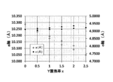
- Table 2 shows the results of calculating the average coordination distance r ave between Ce and N, the excitation wavelength ⁇ ex, and the emission wavelength ⁇ em by changing the substitution amount of Y 3+ .
- FIG. 4 is a graph showing the relationship between the excitation wavelength and the emission wavelength.
- Figure 5 shows the relationship between the lattice constant of the substitution amount x and c-axis of the relationship between the lattice constant of the substitution amount x and the a-axis of Y 3+, and Y 3+.
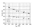
- FIG. 6 shows the relationship between the average coordination distance r ave and the excitation wavelength ⁇ ex and the relationship between the average coordination distance r ave and the emission wavelength ⁇ em .
- FIG. 7 shows a crystal structure of La 3 Si 6 N 11 and two types of sites of La.
- the La (2a) site is indicated by a broken line
- the La (4c) site is indicated by a one-dot chain line.
- 8A to 8J show the crystal structures of Sample Nos. 1 to 10.
- FIG. 9 shows the powder XRD diffraction pattern results calculated from the crystal structures of sample numbers 1 to 10.
- * mark in Table 2 has shown that the sample is a comparative example.
- the Y substitution site and substitution amount are described as “Y substitution site ⁇ Y substitution amount”.
- the emission wavelength tends to increase as the substitution amount of Y 3+ increases. It can also be seen that the excitation peak wavelength also increases as the emission wavelength increases. It can be seen that in the composition systems of Sample 7 to Sample 10 that emit red light having an emission wavelength of 600 nm or more, the excitation wavelength peak is in the green region of 490 nm or more. Further, as apparent from FIG. 5, it can be seen that the a-axis lattice constant decreases and the c-axis lattice constant increases as the substitution amount of Y 3+ increases. Further, as is apparent from Table 2 and FIG. 6, the average coordination distance r ave between Ce and N decreases as the substitution amount of Y 3+ increases, and both the emission wavelength and the excitation wavelength increase as r ave decreases. I understand that
- the emission lifetime of Eu 2+ is very long compared to the emission lifetime of Ce 3+ .
- the emission lifetime correlates with the transition probability of each 4f-5d transition of Eu 2+ Ce 3+, and it can be said that the longer the emission lifetime, the lower the transition probability.
- the excitation probability of the Eu 2+ 4f-5d transition is very low compared to the excitation probability of the Ce 3+ 4f-5d transition.
- Eu 2+ tends to overlap with the conduction band of the base material ((La, Y) 3 Si 6 N 11 ) in the 5d excitation level. Therefore, energy can be efficiently absorbed between the Eu 2 + 4f ground level and the conduction band of the base material. This absorbed energy corresponds to the energy in the blue light region.
- Eu 2+ has seven electrons in the 4f orbit, and the energy level of each electron has a width, so the excitation wavelength is broad. That is, the excitation wavelength of the red phosphor using Eu 2+ as the emission center is a broad excitation wavelength with the blue region as the peak. Therefore, in the light source using the red phosphor using Eu 2+ as the emission center, blue light having the highest absorption efficiency is used as the excitation light source.
- the 5d excitation level hardly overlaps with the conduction band of the host material. Therefore, energy absorption between the 4f ground level and the base material conduction band cannot be expected. Therefore, the 4f-5d transition is the main energy absorber.
- the present inventors have clarified that in the case of a red phosphor using Ce 3+ , the energy difference between 4f-5d transitions is the energy difference in the green light region. Therefore, in the case of a red phosphor using Ce 3+ , the absorption efficiency of the phosphor is higher when green light is used than when blue light is used as the excitation light source. Therefore, the light output can be increased by using green light. Furthermore, compared with the conventional method of converting blue light to red light, the method of the present application that converts green light to red light can reduce energy conversion loss (Stokes loss), and thus higher output. It becomes possible to emit light.
- Stokes loss energy conversion loss
- ⁇ Phosphor of Embodiment 1 From the above results, the present inventors contain a crystal phase having the chemical composition Ce x Y y La 3-xy Si 6 N 11 as a phosphor according to an embodiment of the present disclosure, and 0 ⁇ x ⁇ A new red phosphor with 0.6 and (1.5 ⁇ x) ⁇ y ⁇ (3-x) was reached.
- the phosphor of Embodiment 1 will be described in more detail.
- x satisfies 0 ⁇ x ⁇ 0.6. Since x is larger than 0, light emission by Ce can be obtained.
- x is preferably 0.0003 or more, more preferably 0.015 or more, from the viewpoint of increasing the emission intensity. There is no particular limitation on the maximum value of x as long as the phosphor can emit light. However, when x becomes too large, the emission intensity decreases due to concentration quenching. Therefore, by setting x to 0.6 or less, it is possible to suppress a decrease in light emission intensity. Further, x is preferably 0.3 or less, more preferably 0.15 or less, from the viewpoint of increasing the emission intensity.
- x and y desirably satisfy (1.5 ⁇ 0.5x) ⁇ y ⁇ (3-x), and 1.5 ⁇ y ⁇ (3- It is more desirable to satisfy x).
- the phosphor of Embodiment 1 has an emission spectrum peak in a wavelength range of 600 nm to 660 nm.
- the phosphor of Embodiment 1 may have an emission spectrum peak with a wavelength of 605 nm or more, for example.
- the phosphor of Embodiment 1 may have, for example, an emission spectrum peak with a wavelength of 640 nm or less, and may have an emission spectrum peak with a wavelength of 636 nm.
- the phosphor of Embodiment 1 has an excitation spectrum peak in a wavelength range of 480 nm to 550 nm.
- the phosphor of Embodiment 1 may have, for example, an excitation spectrum peak with a wavelength of 490 nm or more, or an excitation spectrum peak with a wavelength of 495 nm or more.
- the phosphor of the first embodiment may have, for example, an excitation spectrum peak with a wavelength of 530 nm or less, or an excitation spectrum peak with a wavelength of 508 nm or less.
- the phosphor of the first embodiment has the second excitation spectrum peak within the wavelength range of 350 nm to less than 480 nm when the excitation spectrum peak in the wavelength range of 480 nm to 550 nm is used as the first excitation spectrum peak. May further be included.
- the peak of the first or second excitation spectrum may be the maximum peak of the excitation spectrum.
- the 1 / e emission lifetime of the crystal phase of the phosphor of Embodiment 1 may have a value of 100 ns or less.
- the light emission lifetime affects the luminance saturation characteristic.
- a phosphor containing Eu such as CASN: Eu which is a conventional red phosphor, has a longer emission lifetime than a phosphor containing Ce. Therefore, the phosphor containing Eu is likely to be saturated in luminance due to a decrease in quantum efficiency during high output excitation. Therefore, the phosphor of Embodiment 1 having Ce as the emission center is promising as a red phosphor having a high quantum efficiency even at a high output as compared with the conventional red phosphor.
- the crystal of the base material in the phosphor of Embodiment 1 may be a tetragonal crystal.
- the crystal phase having the chemical composition Ce x Y y La 3-xy Si 6 N 11 in the phosphor of Embodiment 1 may have a tetragonal crystal structure.
- the crystal phase may have almost the same crystal structure as the crystal represented by the general formula La 3 Si 6 N 11 .
- the crystal phase of the phosphor according to Embodiment 1 may have a crystal structure in which Ce substitutes at least a part of the La (2a) site in the crystal structure of La 3 Si 6 N 11 .
- the crystal phase of the phosphor of Embodiment 1 may have a crystal structure in which Y substitutes at least a part of the La (4c) site in the crystal structure of La 3 Si 6 N 11 , where Y is La the majority of La (4c) sites in the crystal structure of 3 Si 6 N 11 may have a crystal structure which is substituted.
- the crystal phase of the phosphor of Embodiment 1 has a crystal structure in which Ce substitutes at least a part of the La (2a) site in the crystal structure of La 3 Si 6 N 11 .
- the crystal phase of the phosphor of Embodiment 1 has a crystal structure in which Y substitutes at least part of the La (4c) site in the crystal structure of La 3 Si 6 N 11 . Further, it is more desirable that Y has a crystal structure in which a majority of La (4c) sites in the crystal structure of La 3 Si 6 N 11 are substituted.
- a compound containing Ce, La, Si and Y may be used, or a single substance of Ce, La, Si and Y may be used.
- a compound that becomes a nitride by firing in a nitrogen atmosphere a high-purity (purity 99% or more) nitride, a metal alloy, or the like can be used.
- a small amount of fluoride such as ammonium fluoride may be added.
- the chemical composition ratio represented by Ce x Y y La 3-xy Si 6 N 11 (0 ⁇ x ⁇ 0.6, (1.5 ⁇ x) ⁇ y ⁇ (3-x))
- a Ce compound, a La compound, a Si compound, and a Y compound may be prepared, where a simple substance of Si may be prepared instead of the Si compound, for example, CeF 3 powder, LaN powder, Si 3 N 4 powder, and YN powder may be used, where CeN powder may be used instead of CeF 3 powder, and Si single powder may be used instead of Si 3 N 4 powder.
- LaN powder may be prepared in excess of about 24% of the theoretical value.LaN is easy to decompose during firing, so by adding excessively at the time of blending raw materials, LaSi, which is a by-product, may be used. Generation of 3 N 5 crystals can be suppressed.
- the phosphor of Embodiment 1 is manufactured by mixing and firing the above raw materials.
- the raw material mixing method may be wet mixing in a solution or dry mixing of a dry powder.
- Firing is performed for about 1 to 50 hours in a temperature range of 1500 to 2000 ° C. in an atmosphere pressurized with nitrogen.
- the pressure at this time is usually 3 atmospheres or more, desirably 4 atmospheres or more, and more desirably 8 atmospheres or more.
- the phosphor after firing may be washed, for example, in a nitric acid solution having a concentration of 10% for 1 hour.
- the obtained phosphor powder may be pulverized again using a ball mill, a jet mill or the like, and further washed or classified as necessary to adjust the particle size distribution or fluidity of the phosphor powder.
- the phosphor according to Embodiment 1 can be used in a light emitting device.
- the light emitting device in the present embodiment includes at least an excitation light source and a first phosphor.
- the excitation light source emits light having a wavelength of 600 nm or less.
- the first phosphor is irradiated with light emitted from the excitation light source and emits fluorescence having a longer wavelength than the light emitted from the excitation light source.
- the first phosphor is, for example, any of the phosphors described in the first embodiment. According to the above configuration, a light emitting device with high quantum efficiency can be configured even at high output.
- the light emitted from the excitation light source may have a wavelength of 480 nm to 600 nm. Since the phosphor of the first embodiment typically has an excitation spectrum peak in the wavelength range of 480 nm to 550 nm, it can be efficiently excited by using an excitation light source that emits light in the above wavelength range. Can do.
- the light emitted from the excitation light source may include light with a wavelength of 200 nm to 480 nm, or may include light with a wavelength of 420 nm to 480 nm.
- the phosphor of Embodiment 1 can absorb excitation light even at a wavelength of 480 nm or less.
- an excitation light source that emits light with a wavelength of 200 nm or more is desirable.
- said excitation light source LED or LD is mentioned, for example.
- the light emitting device in the present embodiment may further include a second phosphor having an emission spectrum peak within a wavelength range of 500 nm to 600 nm. That is, the light emitting device may include a combination of the first phosphor and the second phosphor.
- the second phosphor emits fluorescence having a longer wavelength than the light emitted from the excitation light source when irradiated with the light emitted from the excitation light source.
- a phosphor containing a crystal phase may be used.
- the second phosphor may be a phosphor that emits yellow light, for example.
- the light emitting device may further include a third phosphor that emits green light. That is, the light emitting device may include a combination of a first phosphor, a second phosphor that emits yellow light, and a third phosphor that emits green light.
- the third phosphor emits fluorescence having a longer wavelength than the light emitted from the excitation light source when irradiated with the light emitted from the excitation light source.
- a phosphor containing a crystal phase of the chemical composition Lu 3 Al 5 O 12 : Ce (LuAG: Ce), or a chemical composition Y 3 (Al, Ga) 5 N 12: Ce (YAGG: A phosphor containing a crystal phase having Ce) may be used.
- Green light means light located in the range of (0.1 ⁇ x ⁇ 0.4, 0.5 ⁇ y ⁇ 0.8) in the CIE chromaticity coordinate values.
- Yellow light refers to light positioned in the range of (0.4 ⁇ x ⁇ 0.6, 0.4 ⁇ y ⁇ 0.6) in the CIE chromaticity coordinate values.
- the excitation light source and the second and third phosphors can be freely selected within the above-described range according to the use of the light emitting device. Therefore, the light emitting device including the phosphor according to Embodiment 1 is useful not only as a red light emitting device but also as a white light emitting device. Specifically, a combination of an excitation light source that emits blue light, a phosphor that emits yellow light, and the red phosphor of the present embodiment emits light in a high-color rendering high-output light-emitting device or light bulb color. A high-output light emitting device can be realized.
- Embodiment 2 demonstrates the LED light-emitting device which uses the LED chip as a light emitting element as a light source as an example of the light-emitting device of this indication.
- FIG. 10 is a schematic cross-sectional view showing an embodiment of the LED light-emitting device of Embodiment 2.
- the LED light emitting device 10 includes a phosphor 11, an LED chip 15, and an LED sealing body 24. Further, the LED light emitting device 10 may include a support 23.
- the support body 23 supports the LED chip 15. In this embodiment, since the LED light-emitting device 10 has a structure that can be surface-mounted, the support 23 is a substrate.
- This embodiment can be used for a high-luminance LED light-emitting device.
- the support 23 has a high thermal conductivity so that heat generated in the LED chip 15 can be efficiently radiated to the outside.
- a ceramic substrate made of alumina or aluminum nitride can be used as the support 23.
- the LED chip 15 for example, one that emits light in the ultraviolet to yellow region is used, and one that has an emission spectrum peak within a wavelength range of 200 nm to 600 nm is used. Specifically, a yellow LED chip, a green LED chip, a blue LED chip, a blue-violet LED chip, a near ultraviolet LED chip, an ultraviolet LED chip, or the like is used as the LED chip 15.
- the LED chip 15 is fixed to the support 23 with solder 27 or the like so that the emission surface 15 a does not come into contact with the support 23 on the support 23.
- the LED chip 15 is electrically connected to an electrode 22 provided on the support 23 by a bonding wire 21.
- the LED chip 15 is covered with an LED sealing body 24.
- silicone resin is used for the LED sealing body 24.
- the phosphor 11 is dispersed in the LED sealing body 24.
- the silicone resin a silicone resin having a structure defined by various chemical formulas used as a sealing resin for a semiconductor light emitting device can be used.
- the silicone resin contains, for example, dimethyl silicone having high discoloration resistance.
- methylphenyl silicone etc. with high heat resistance can also be used as a silicone resin.
- the silicone resin may be a homopolymer having a main skeleton with a siloxane bond defined by one chemical formula.
- regulated by 2 or more types of chemical formula, and the alloy of 2 or more types of silicone polymers may be sufficient.
- the silicone resin in the LED sealing body 24 is in a state after being cured. Therefore, the LED sealing body 24 is also in a cured state.
- the LED sealing body 24 can be manufactured using an uncured silicone resin.
- the silicone resin is generally a two-component type in which curing is accelerated by mixing a main agent and a curing agent.
- a thermosetting silicone resin or an energy curable silicone resin that cures when irradiated with energy such as light can also be used.
- FIG. For example, you may use the inorganic material etc. which are comprised from glass, an epoxy resin, ZnO.
- the phosphor 11 may be arranged on the LED sealing body 24 in the form of a phosphor plate without being dispersed in the LED sealing body 24.
- the LED chip is wire bonded, but the LED chip used in the present embodiment may have other configurations. That is, the LED chip used in the present embodiment may be mounted face-up or mounted by flip chip. Moreover, the LED chip used in the present embodiment may include a light emitting layer formed of a nitride semiconductor having a general polar plane (c-plane) growth surface.
- c-plane general polar plane
- the phosphor 11 absorbs a part of wavelength components or all wavelength components in the near ultraviolet to yellow region light (for example, near ultraviolet light) emitted from the LED chip 15 and emits fluorescence.
- the wavelength of light to be absorbed and the wavelength of fluorescence are determined by the type of fluorescent material contained in the phosphor 11.
- the phosphor 11 may be a mixed phosphor including a plurality of phosphors of different colors so that white light is created by the color mixture of light.
- the phosphor 11 may be a mixed phosphor of a green phosphor and a red phosphor. As the red phosphor, the phosphor of the first embodiment is used.
- the phosphor 11 may be a mixed phosphor of a yellow phosphor and a red phosphor.
- the red phosphor the phosphor of the first embodiment is used.
- the yellow phosphor include Y 3 Al 5 O 12 : Ce 3+ , CaSi 2 O 2 N 2 : Eu 2+ , (Ba, Sr) Si 2 O 2 N 2 : Eu 2+ , and Ca 3 Sc 2 Si 3 O.
- Phosphors such as 12 : Ce 3+ , CaSc 2 O 4 : Ce 3+ , ⁇ -SiAlON: Eu 2+ , La 3 Si 6 N 11 : Ce 3+ can be used.
- the particle diameter of the phosphor 11 is, for example, 1 ⁇ m or more and 80 ⁇ m or less, respectively.
- the particle diameter means a circle equivalent diameter measured by a microscopic method.
- the phosphor 11 is included in the LED sealing body 24 at a ratio of 3 parts by weight to 70 parts by weight with respect to 100 parts by weight of the sealing body, for example.
- the weight ratio of the phosphors that emit light of each color used in the phosphor 11 can be appropriately determined according to the desired color tone of white light and the emission intensity of each phosphor.
- the LED light emitting device is configured as an LED light emitting device that emits a color other than white by using only the red phosphor of the first embodiment or combining the phosphor 11 with another color phosphor. You can also.
- the above-described phosphors other than the red phosphor of Embodiment 1 can be manufactured according to a known method. Specifically, in the case of producing an oxide phosphor, as a raw material, a compound that becomes an oxide by firing, such as hydroxide, oxalate, or nitrate, or an oxide can be used. Here, in order to accelerate the reaction, a small amount of fluoride (for example, calcium fluoride) or chloride (for example, calcium chloride) can be added. The phosphor is manufactured by mixing and firing the above raw materials.
- the mixing method of the raw materials may be wet mixing in a solvent or dry mixing of dry powder.
- a ball mill, a medium stirring mill, a planetary mill, a vibration mill, a jet mill, a V-type mixer, a stirrer and the like that are usually used industrially can be used.
- the phosphor material is fired in the air or in a reducing atmosphere at a temperature range of 1100 to 1700 ° C. for about 1 to 50 hours.
- the furnace used for baking can use the furnace normally used industrially.
- a continuous or batch electric furnace such as a pusher furnace or a gas furnace, or a pressure firing furnace such as plasma sintering (SPS) or hot isostatic pressing (HIP) can be used.
- SPS plasma sintering
- HIP hot isostatic pressing
- FIG. 11 shows a schematic configuration of the LD light emitting device 60 according to the third embodiment.
- the LD light emitting device 60 includes an LD element 58 and a wavelength conversion member 61.
- the wavelength conversion member 61 includes a phosphor. The phosphor converts the light emitted from the LD element 58 into light having a longer wavelength.
- the LD element 58 can emit light having a higher optical power density than the LED. Therefore, the use of the LD element 58 can constitute a high-power LD light emitting device 60.
- the optical power density applied to the phosphor from the LD element 58 is, for example, 0.5 W / mm 2 or more. Further, the optical power density is irradiated onto the phosphor may also be 2W / mm 2 or more, may also be 3W / mm 2 or more, may be at 10 W / mm 2 or more.
- the light power density applied to the phosphor may be 150 W / mm 2 or less, 100 W / mm 2 or less, 50 W / mm 2 or less, or 20 W / mm 2. It may be the following.
- an element that emits light having a wavelength capable of exciting the phosphor can be used without particular limitation.
- an LD element that emits blue-violet light, an LD element that emits blue light, an LD element that emits green light, an LD element that emits yellow light, or the like can be used.
- blue light means light having a peak wavelength of 420 nm or more and less than 480 nm.
- the LD element 58 that emits blue light has higher luminous efficiency than the LD element that emits ultraviolet light, and has the highest luminous efficiency when the emission peak wavelength is 445 nm.
- the emission peak wavelength of the LD element 58 may be 425 nm or more, or 430 nm or more. On the other hand, the emission peak wavelength of the LD element 58 may be 475 nm or less, or 470 nm or less.
- the LD element 58 may be composed of one LD, or may be one in which a plurality of LDs are optically coupled.
- the LD element 58 may include a light emitting layer formed of a nitride semiconductor having a growth surface that is a nonpolar surface or a semipolar surface.
- the phosphor of the wavelength conversion member 61 includes the red phosphor of the first embodiment.
- the wavelength conversion member 61 may further include a phosphor other than the red phosphor of the first embodiment according to a desired emission color of the light emitting device.
- the LD light emitting device 60 can be configured as a white light emitting device.
- yellow fluorescent substance and green fluorescent substance what was illustrated in Embodiment 2 can be used.
- the wavelength conversion member 61 may be a single wavelength conversion layer in which a plurality of types of phosphors are mixed, and is a laminate in which at least two wavelength conversion layers including a single type or a plurality of types of phosphors are stacked. May be.
- the wavelength conversion member 61 having a configuration in which a first phosphor layer 62 composed of the red phosphor 12 and a second phosphor layer 63 composed of the yellow phosphor 13 are laminated. The case where is used will be described.
- the first phosphor layer 62 and the second phosphor layer 63 are configured using binders 68 and 69, respectively.
- the binders 68 and 69 are media, such as resin, glass, or a transparent crystal, for example.
- the binders 68 and 69 may be made of the same material or different materials.
- Each phosphor layer may be composed only of phosphor particles.
- An incident optical system 59 that guides the light of the LD element 58 to the second phosphor layer 63 may be provided between the wavelength conversion member 61 and the LD element 58.
- the incident optical system 59 includes, for example, a lens, a mirror, or an optical fiber.
- the blue light emitted from the LD element 58 passes through the incident optical system 59 and enters the second phosphor layer 63 of the wavelength conversion member 61.
- the incident light excites the plurality of yellow phosphors 13 in the second phosphor layer 63 to emit yellow light.
- the blue light emitted from the LD element 58 that has been transmitted without being absorbed by the second phosphor layer 63 is incident on the first phosphor layer 62.
- the plurality of red phosphors 12 in the first phosphor layer 62 are excited and emit red light.
- yellow light emitted from the second phosphor layer 63 is incident on the first phosphor layer 62.
- a part of the incident light may excite the plurality of red phosphors 12 of the first phosphor layer 62 to emit red light. Further, the blue light emitted from the LD element 58 that is transmitted without being absorbed by the first phosphor layer 62 and the second phosphor layer 63 is emitted to the outside. These red light, yellow light, and blue light are mixed to become white light.
- each phosphor layer may be adjusted so that the blue light emitted from the LD element 58 does not pass through the first phosphor layer 62. Further, it may be adjusted so that yellow light emitted from the second phosphor layer 63 does not pass through the first phosphor layer 62. In this case, only red light is emitted to the outside.
- the green phosphor described in the second embodiment may be used in place of the yellow phosphor 13 used in the second phosphor layer 63.
- FIG. 12 shows a schematic configuration of the LD light emitting device 80 according to the fourth embodiment.
- the LD light emitting device 80 includes an LD element 58 and a wavelength conversion member 81.
- the wavelength conversion member 81 includes a phosphor.
- the phosphor converts the light emitted from the LD element 58 into light having a longer wavelength.
- the phosphor of the wavelength conversion member 81 has a wavelength conversion layer in which the red phosphor 12 and at least one selected from the group consisting of the yellow phosphor 13 and the green phosphor 14 are mixed.
- the red phosphor 12 the phosphor of the first embodiment is used.
- yellow fluorescent substance and green fluorescent substance what was illustrated in Embodiment 2 can be used.
- the wavelength conversion member 81 is a phosphor layer formed by mixing three kinds of the red phosphor 12, the yellow phosphor 13, and the green phosphor 14 will be described.
- the mixing ratio of the three types of phosphors can be appropriately adjusted according to the desired color tone of white light, the emission intensity of each phosphor, and the like.
- the phosphor layer that is the wavelength conversion member 81 is configured using a binder 68.
- the binder 68 is a medium such as resin, glass, or transparent crystal.
- the binder 68 may be a single material or may be a different material depending on the location. Note that the phosphor layer may be composed of only phosphor particles.
- the blue light emitted from the LD element 58 passes through the incident optical system 59 and is red, yellow, and green light by the red phosphor 12, the yellow phosphor 13, and the green phosphor 14 in the wavelength conversion member 81, respectively. Is converted to The blue light emitted from the LD element 58 that has not been absorbed by the phosphor is mixed with the red light, yellow light, and green light converted by the red phosphor 12, the yellow phosphor 13, and the green phosphor 14, respectively. White light.
- the red phosphor 12 is excited by part of the green light emitted from the green phosphor 14 and emits red light.
- Embodiment 5 demonstrates an example of the illuminating device of this indication.
- FIG. 13 shows a schematic configuration of the illumination device 120 according to the fifth embodiment.
- the illumination device 120 includes a light source 121 and an output optical system 122 that guides light emitted from the light source 121 forward.
- a wavelength cut filter 123 that absorbs or reflects light from the light source may be provided.
- the light source 121 includes the red phosphor according to the first embodiment.
- the light source 121 may be the light emitting device 10, 60, or 80 of the second to fourth embodiments.
- the output optical system 122 may be a reflector, for example.
- the emission optical system 122 may include, for example, a metal film such as Al or Ag, or an Al film having a protective film formed on the surface.
- the quantum efficiency can be improved compared to the conventional illumination device at high output. Furthermore, when configured as a white illumination device, high color rendering and color reproducibility can be realized.
- FIG. 14 shows a schematic configuration of the illumination device 130 according to the sixth embodiment.
- the illumination device 130 includes an LD element 58, an incident optical system 59, an optical fiber 132, a wavelength conversion member 131, and an output optical system 122.
- the light emitted from the LD element 58 is guided to the optical fiber 132 through the incident optical system 59.
- the optical fiber 132 guides the light to the emission part.
- the emission unit includes, for example, a wavelength conversion member 131 and an emission optical system 122.
- the wavelength conversion member 131 includes the red phosphor according to the first embodiment. Further, the wavelength conversion member 131 may be the wavelength conversion member 61 or 81 of the third to fourth embodiments.
- the wavelength conversion member 131 may be positioned on the exit side of the optical fiber 132 as shown in FIG. 14, but is on the incident side of the optical fiber 132 (for example, between the LD element 58 and the incident optical system 59, or (Between the incident optical system 59 and the optical fiber 132).
- the light irradiation direction can be easily changed by using an optical fiber.
- the red phosphor of the first embodiment is used, the quantum efficiency can be improved as compared with the conventional illumination device at the time of high output. Furthermore, when configured as a white illumination device, high color rendering and color reproducibility can be realized.
- FIG. 15 shows a schematic configuration of a vehicle 140 according to the seventh embodiment.
- the vehicle 140 includes a vehicle headlamp that is the illumination device 120 of the fifth embodiment, and a power supply source 141.
- the vehicle 140 may include a generator 142 that is rotated by a drive source such as an engine and generates electric power.
- the power generated by the generator 142 may be stored in the power supply source 141.
- the power supply source 141 may be a secondary battery that can be charged and discharged.
- the lighting device 120 is turned on by the power from the power supply source 141.
- the vehicle 140 is, for example, an automobile, a motorcycle, or a special vehicle.
- the vehicle 140 may be an engine vehicle, an electric vehicle, or a hybrid vehicle.
- the vehicle headlamp including the red phosphor of the first embodiment since the vehicle headlamp including the red phosphor of the first embodiment is used, it is possible to illuminate the front more brightly than before when the output is high. Furthermore, when configured as a white illumination device, high color rendering and color reproducibility can be realized.
- the phosphor of the present disclosure is useful as a light emitting device.
- the phosphor of the present disclosure includes, for example, a general lighting device such as a ceiling light, a spotlight, a special lighting device such as a stadium lighting, a studio lighting, a vehicle lighting device such as a headlamp, a projector, a head-up display, etc.
Abstract
本開示の一態様に係る蛍光体は、化学組成CexYyLa3-x-ySi6N11を有する結晶相を含有し、0<x≦0.5であり、(1.5-x)≦y≦(3-x)であり、波長600nm以上660nm以下の範囲内に発光スペクトルのピークを有し、波長480nm以上600nm以下の範囲内に励起スペクトルの第一のピークを有する。
Description
本開示は、蛍光体および発光装置に関する。
近年、白色LED(Light Emitting Diode)、レーザー励起光源などの固体光源が広く用いられるようになってきている。現在の一般的な白色LEDは、青色発光素子である青色LEDチップと蛍光体を組み合わせた構成を有している。このような一般的な白色LEDでは、青色LEDチップからの光の一部を蛍光体で色変換し、青色LEDチップからの青色光と蛍光体からの発光とを混色して白色光が作り出されている。より近年では、LD(Laser Diode)と蛍光体との組み合わせによる高出力白色発光装置の開発も行われている。白色固体光源としては、現在、青色LEDチップまたは青色LDと黄色蛍光体との組み合わせが主流である。演色性、色再現性等を高める目的、あるいは色温度の低い白色を得る目的で、青色光源と黄色蛍光体とに加えて赤色蛍光体を組み合わせた白色光源の開発が行われている。
従来、一般式Y3Al5O12:Ce3+(以下YAG:Ceと略する)、または特許文献1に示されている一般式La3Si6N11:Ce3+(以下LSN:Ceと略する)のように、Ceを発光中心とした黄色蛍光体が知られている。また、特許文献2に示されている一般式(Sr,Ca)AlSiN3:Eu2+(以下CASN:Euと略する)のように、Euを発光中心とした赤色蛍光体が知られている。
本開示は、Ceを発光中心とした蛍光体を提供する。
本開示の一態様における蛍光体は、化学組成CexYyLa3-x-ySi6N11を有する結晶相を含有し、0<x≦0.6であり、(1.5-x)≦y≦(3-x)であり、波長600nm以上660nm以下の範囲内に発光スペクトルのピークを有し、波長480nm以上550nm以下の範囲内に励起スペクトルの第一ピークを有する。
本開示の包括的または具体的な態様は、蛍光体、素子、装置、システム、車両、方法、または、これらの任意な組み合わせで実現されてもよい。
本開示によれば、Ceを発光中心とした蛍光体を実現することができる。
(本開示の基礎となった知見)
LEDを用いた白色発光装置としては、以下の方式の装置が考えられる。
LEDを用いた白色発光装置としては、以下の方式の装置が考えられる。
一つ目は、青色LEDと黄色蛍光体YAG:Ceとを組み合わせた擬似白色光源である。この方式の発光装置は、消費電力を低減することができ、LEDの駆動制御を容易に行えることから広く使用されている。しかしながら、この白色光源では色成分が2色しかないため、電球色などの暖かみのある光を演出することができず、色制御が困難である。
二つ目は、青色LEDと黄色蛍光体YAG:Ceと赤色蛍光体CASN:Euとを組み合わせた白色光源である。この方式の発光装置では、白色が3色の色成分の混色であるため、色成分それぞれの光強度を調整することで任意の白色光を演出することができる。したがって、この方式の発光装置は、色成分が2色である前述の方式の発光装置と比較すると、色制御が容易である。この発光装置に用いられる黄色蛍光体YAG:Ceは、発光の量子効率が高く、また高出力の青色LEDあるいは青色LDで励起しても発光の量子効率がほとんど変化しない。一方、赤色蛍光体CASN:Euは、高出力光で励起すると発光の量子効率が低下するという問題があり、比較的低出力の光源にしか搭載されていない。これは、Euを発光中心とした蛍光体は、Ceを発光中心とした蛍光体と比較して発光寿命が長いため、高出力励起時に輝度飽和しやすいためである。そのため、従来、高出力かつ色制御が容易な白色光源を実現することができなかった。
そこで、高出力の光放射が可能であり、色制御が容易な白色光を放射する発光装置を実現するために、本発明者らは、Ceを発光中心とした赤色蛍光体を得るべく、鋭意研究した。
(本開示に係る一態様の概要)
本開示の第1の態様に係る蛍光体は、化学組成CexYyLa3-x-ySi6N11を有する結晶相を含有し、0<x≦0.6であり、(1.5-x)≦y≦(3-x)であり、波長600nm以上660nm以下の範囲内に発光スペクトルのピークを有し、波長480nm以上550nm以下の範囲内に励起スペクトルの第一ピークを有する。
本開示の第1の態様に係る蛍光体は、化学組成CexYyLa3-x-ySi6N11を有する結晶相を含有し、0<x≦0.6であり、(1.5-x)≦y≦(3-x)であり、波長600nm以上660nm以下の範囲内に発光スペクトルのピークを有し、波長480nm以上550nm以下の範囲内に励起スペクトルの第一ピークを有する。
本開示の第1の態様によれば、Ceを発光中心とした蛍光体を実現することができる。
第2の態様において、例えば、第1の態様に係る蛍光体の前記xおよび前記yが、(1.5-0.5x)≦y≦(3-x)を満たしてよい。
第2の態様に係る蛍光体によれば、発光波長および励起波長の長波長化を実現できる。
第3の態様において、例えば、第2の態様に係る蛍光体の前記xおよび前記yが、1.5≦y≦(3-x)を満たしてよい。
第3の態様に係る蛍光体によれば、発光波長および励起波長のさらなる長波長化を実現できる。
第4の態様において、例えば、第1から第3の態様の少なくともいずれか1つの態様に係る蛍光体では、前記結晶相が正方晶(テトラゴナル)の結晶構造を有してよい。
第5の態様において、例えば、第1から第4の態様の少なくともいずれか1つの態様に係る蛍光体は、波長350nm以上480nm未満の範囲内に前記励起スペクトルの第二のピークを有してよい。
第5の態様に係る蛍光体は、例えば青色LEDの450nmや青紫LDの405nm等の、より短波長の励起光でも発光させることができるため、励起光源の選択肢が広がる。
第6の態様において、例えば、第1から第5の態様の少なくともいずれか1つの態様に係る蛍光体の前記結晶相の1/e発光寿命が、100ns以下であってよい。
第6の態様に係る蛍光体は、輝度飽和特性に優れているので、高出力時でも量子効率が高い赤色蛍光体として有望である。
第7の態様において、例えば、第1から第6の態様の少なくともいずれか1つの態様に係る蛍光体の前記結晶相が、CeがLa3Si6N11の結晶構造におけるLa(2a)サイトの少なくとも一部を置換している結晶構造を有してよい。
第7の態様に係る蛍光体は、より長波長の励起光でも発光させることができるため、例えば緑色励起光源との組み合わせに適している。
第8の態様において、例えば、第1から第7の態様の少なくともいずれか1つの態様に係る蛍光体の前記結晶相が、YがLa3Si6N11の結晶構造におけるLa(4c)サイトの少なくとも一部を置換している結晶構造を有してよい。
第8の態様に係る蛍光体では、YがLa3Si6N11の結晶構造におけるLa(4c)サイトの少なくとも一部を置換しているので、結晶格子のa軸とb軸の格子定数が減少し、相対的にc軸が伸びる。このため、格子ひずみが増加し、その結果、4f-5d軌道間のエネルギー差が減少して、発光波長が長波長化され得る。
第9の態様において、例えば、第8の態様に係る蛍光体の前記結晶相が、YがLa3Si6N11の結晶構造におけるLa(4c)サイトの過半数を置換している結晶構造を有してよい。
第9の態様に係る蛍光体では、結晶ひずみが急増し、その結果、長波長側への波長シフトが急増するので、赤色発光が可能となる。
本開示の第10の態様に係る発光装置は、波長600nm以下の光を発する励起光源と、第1から第9の態様の少なくともいずれか1つの態様に係る蛍光体である第一の蛍光体と、を備える。前記第一の蛍光体は、前記励起光源の発する光を照射され、前記光よりも長波長の蛍光を発する。
第10の態様に係る発光装置は、第1から第9の態様の少なくともいずれか1つの態様に係る蛍光体を備えているので、高出力時において従来の発光装置よりも量子効率を向上させることができる。さらに、第10の態様に係る発光装置を白色発光装置として構成した場合には、高い演色性および色再現性を実現できる。
第11の態様において、例えば、第10の態様に係る発光装置の前記励起光源が、波長480nm以上600nm以下の光を発してよい。
第11の態様に係る発光装置によれば、蛍光体を効率的に励起することができる。
第12の態様において、例えば、第10の態様に係る発光装置の前記励起光源が、波長420nm以上480nm以下の光を発してよい。
第12の態様に係る発光装置によれば、GaN系の青色LEDや青色LDを励起光源として使用することができる。
第13の態様において、例えば、第10から第12の態様の少なくともいずれか1つの態様に係る発光装置は、前記励起光源がLEDまたはLDであってよい。
第13の態様によれば、高出力の発光装置を実現できる。
第14の態様において、例えば、第10から第13の態様の少なくともいずれか1つの態様に係る発光装置は、前記励起光源の発する光を照射され、前記光よりも長波長の蛍光を発する第二の蛍光体をさらに備えてよく、前記第二の蛍光体が、波長480nm以上600nm未満の範囲内に発光スペクトルのピークを有してよい。
第14の態様の発光装置は、発光波長が異なる少なくとも2種類の蛍光体を備えているので、発光色を制御することができる。
第15の態様において、例えば、第14の態様に係る発光装置は、前記第二の蛍光体が黄色光を発する蛍光体であり、前記励起光源の発する光を照射され、前記光よりも長波長の蛍光を発する第三の蛍光体をさらに備えてよく、前記第三の蛍光体が緑色光を発してよい。
第15の態様の発光装置は、黄色光を発する蛍光体と緑色光を発する蛍光体との少なくとも2種類の蛍光体を備えているので、発光色を制御することができる。
(本開示の実施の形態)
以下、本開示の実施の形態について詳細に説明する。当然ながら、本開示はこれらの実施形態に限定されるものでなく、本開示の技術的範囲を逸脱しない範囲で適宜変更して実施することができる。
以下、本開示の実施の形態について詳細に説明する。当然ながら、本開示はこれらの実施形態に限定されるものでなく、本開示の技術的範囲を逸脱しない範囲で適宜変更して実施することができる。
[実施形態1]
実施形態1では、本開示の蛍光体の実施形態について説明する。以下に、本発明者らが本開示の蛍光体に到達した経緯を含め、本開示の蛍光体の実施形態について説明する。
実施形態1では、本開示の蛍光体の実施形態について説明する。以下に、本発明者らが本開示の蛍光体に到達した経緯を含め、本開示の蛍光体の実施形態について説明する。
<希土類蛍光体の発光原理>
以下に、本発明者らが、希土類蛍光体の発光原理について考察を行い、Ce3+蛍光体に着目した経緯について説明する。
以下に、本発明者らが、希土類蛍光体の発光原理について考察を行い、Ce3+蛍光体に着目した経緯について説明する。
希土類元素のうちCe、Pr、Nd、Pm、Sm、Eu、Gd、Tb、Dy、Ho、Er、TmおよびYbは、2価または3価のイオンの状態で、4f軌道に価電子を有する。このうち、ほとんどの希土類イオンは4fに複数の電子を有するので、図1Aに概念的に示したように4f軌道の縮退が解けて大きく分裂する。これにより、ある4f準位から別の4f準位への遷移(f-f遷移)を利用して発光を得ることができる。f-f遷移は禁制遷移であるため、励起状態の電子の寿命が長いという特徴を有している。そのため、希土類イオンを含む蛍光体は、レーザー媒質としてよく利用されている。しかしながら、このような蛍光体を一般の照明などのインコヒーレントな光源として利用すると、すぐに発光強度が飽和してしまう。
一方、Ce3+は、価電子として4f軌道に1つしか電子を有さない。これにより、図1Bに概念的に示したように、Ce3+の4f軌道の分裂は他の希土類イオンに比べて極めて小さい。また、例外として、Eu2+およびYb2+の4f軌道のエネルギー分裂も小さい。これは、Eu2+が4f軌道に7つの電子を有する半閉殻であり、および、Yb2+が4f軌道に14の電子を有する閉殻であるためである。
Ce3+、Eu2+およびYb2+は4f軌道の分裂が小さいため、4f基底準位と5d軌道との間のエネルギー差が大きい。また、4f基底準位と5d軌道との間に大きなエネルギーを持つ4f軌道が存在しない。よって、4fと5dとの間の遷移(4f-5d遷移)を利用しやすい。
4f-5d遷移は許容遷移であるため、励起状態の電子の寿命が短い。従って、励起すればすぐに発光するため、強い励起光で励起しても飽和(輝度飽和)しにくい。
本発明者らは、さらに、Ce3+、Eu2+およびYb2+のうちCe3+に着目した。Ce3+は4f-5d遷移に関わる電子は1つであるため、5dの励起状態から4fの基底状態に落ちる際に、4fの軌道が全て空いている、すなわち遷移に関わる4f軌道の状態密度が大きい。このため、本発明者らは、Ce3+は発光寿命が最も短いと考えた。一方、Eu2+は、5dに電子を励起しても4fに6つの電子が残っており、Yb2+は、5dに電子を励起しても4fに13つの電子が残っている。このため、Eu2+およびYb2+は、4f軌道の状態密度が小さく、Ce3+よりも長い発光寿命を有すると予測できる。従って、Ce3+蛍光体は希土類の中で最も発光寿命が短く、輝度飽和しにくいと考えられる。実際に、YAG:Ceでは1/e発光寿命が70ns程度であるのに対して、CASN:Euでは1/e発光寿命が600から800ns程度である。
この考えに基づけば、Ce3+蛍光体の方がEu2+蛍光体よりも優れていると言える。実際に、市販されている白色LEDでは、ほぼ全てにYAG:Ceが利用されている。しかしながら、赤色蛍光体としてはCASN:Euがよく使われている。本発明者らは、この理由として、赤色発光するCe3+蛍光体の実現は難しく、未だ有望な材料が見つかっていないからであると考えている。以下に、発光波長が決まる原理とともに、その理由を説明する。
<蛍光体の発光波長>
Ce3+を発光中心とする蛍光体およびEu2+発光中心とする蛍光体においては、基底状態である4f軌道から励起状態である5d軌道への遷移(4f-5d遷移)を利用する。Ce3+およびEu2+が蛍光体の母体となる結晶に導入されると、主に結合している最近接のアニオン原子(配位子)の影響を受け、4fおよび5d軌道のエネルギーが変化し、発光波長が変わる。すなわち、蛍光体の発光波長は、母体結晶によって決まる。
Ce3+を発光中心とする蛍光体およびEu2+発光中心とする蛍光体においては、基底状態である4f軌道から励起状態である5d軌道への遷移(4f-5d遷移)を利用する。Ce3+およびEu2+が蛍光体の母体となる結晶に導入されると、主に結合している最近接のアニオン原子(配位子)の影響を受け、4fおよび5d軌道のエネルギーが変化し、発光波長が変わる。すなわち、蛍光体の発光波長は、母体結晶によって決まる。
配位子の影響としては、4fまたは5d軌道のエネルギーがシフトすること、および5d軌道の5つの準位の縮退が解けること(すなわち、5d軌道の分裂)がある。前者のエネルギーシフトについては、4fまたは5d軌道の波動関数の広がり方と配位子の位置関係とが大きく影響する。また、後者の5d軌道の分裂に関しては、図2に示すように5d軌道の5つの準位のトータルエネルギーを保ったまま5d軌道が分裂する。よって、ある準位のエネルギーが大きくなれば、他の準位のエネルギーは小さくなる。従って、5d軌道の分裂を大きくすることで、5d軌道の最低エネルギーを小さくすることができる。
4f-5d遷移の発光は、図2に示すように5d軌道の最低エネルギーの準位から4fに落ちる際に起きる。このため、Ce3+またはEu2+を結晶に導入することで、4f-5d間のエネルギー差を小さくし、発光波長を長波長化することができる。
Ce3+は真空中(すなわち、結晶に未導入の状態)においては4f-5d間のエネルギー差が大きく深紫外域の発光を示すが、Eu2+は青色発光を示す。即ち、Eu2+の方が少ない長波長シフト量で赤色発光が実現でき、実際にCASN:Euが実用化されている。一方、Ce3+蛍光体で実用化されている最も長波長なものは黄色蛍光体のYAG:Ceであり、赤色蛍光体は実現されていない。
<発明者らの検討>
本発明者らは、Ceの赤色蛍光体を実現するためには、図3に示すように、5d軌道または4f軌道をシフトさせる必要があると考え、検討を進めた。
本発明者らは、Ceの赤色蛍光体を実現するためには、図3に示すように、5d軌道または4f軌道をシフトさせる必要があると考え、検討を進めた。
より5d軌道または4f軌道をシフトさせるためには、Ce3+の配位子として、(1)配位子距離が小さいこと、および(2)配位子の対称性が低いこと、を満たすことが重要であると考えた。
まず(1)に関して、Ce3+から最近接のアニオンまでの配位子距離が小さいと、4f軌道または5d軌道のいずれか、あるいは両方がアニオンの軌道からより大きく影響を受け、大きくエネルギーシフトする。このとき4f軌道のエネルギーが増加する、あるいは5d軌道の分裂が大きくなり5d軌道の最低エネルギー準位が下がる。この効果により4f-5d間のエネルギー差が小さくなる。(2)に関しては、配位子の対称性が低いことで、配位子が存在しない方向への広がりが大きい波動関数を持つ5d軌道がより安定化される。これにより、4f-5d間のエネルギー差が小さくなる。
本発明者らは、これらの方針のもとに新しい材料の探索を行った。具体的には、結晶構造シミュレーションにより発光波長を計算する検討を行った。これらの取り組みで、赤色を示す複数の新規赤色蛍光体に到達した。以下でこれらの取り組みについて説明する。
<Ce蛍光体の発光波長の計算について>
本発明者らは、Ceを発光中心として用いた蛍光体の発光波長と励起波長との関係を明らかにするため、シミュレーションにより各種の結晶にCeをドープした場合の発光波長と励起波長とについて検討を行った。以下に、結晶構造シミュレーションの結果および考察を示す。
本発明者らは、Ceを発光中心として用いた蛍光体の発光波長と励起波長との関係を明らかにするため、シミュレーションにより各種の結晶にCeをドープした場合の発光波長と励起波長とについて検討を行った。以下に、結晶構造シミュレーションの結果および考察を示す。
本発明者らは、文献「Y Jia et al., PHYSICAL REVIEW B 93, 155111 (2016)」に開示されている手法で発光波長の計算を行った。この手法は、基底状態の平衡点における全エネルギーとその原子座標での励起状態の全エネルギーとの差から励起波長を計算する。また、この手法は、励起状態が緩和した平衡点における全エネルギーとその原子座標での基底状態の全エネルギーとの差から発光波長を計算する。これにより、上記文献によると、YAG:Ce、LaSi3N5:Ce、La3Si6N11:Ceの3種類の蛍光体の発光波長と励起波長との計算値が実験値とほぼ一致することが確認されている。今回、本発明者らが、LaSi3N5:Ce、La3Si6N11:Ceに加えてYAlO3:Ceについて発光波長と励起波長との計算を行ったところ、上記文献と同様に高精度に実験結果を再現することを確認した。表1にシミュレーションにより求めた各蛍光体の励起波長と発光波長とを示す。

<新規組成系(La,Y)3Si6N11:Ce蛍光体>
まず、本発明者らは、配位子距離を短くするために、La3Si6N11:CeのLa3+サイトにY3+を置換することを考えた。
まず、本発明者らは、配位子距離を短くするために、La3Si6N11:CeのLa3+サイトにY3+を置換することを考えた。
Y3+はLa3+に比べてイオン半径が小さいために、La3+サイトを置換すれば格子定数を小さくする可能性がある。格子定数の低下に伴い、配位子距離も短くすることができる期待がある。
上記の計算手法により、新規組成系である(La,Y)3Si6N11:Ce蛍光体について検討を行った。この組成系の蛍光体は、La3Si6N11:CeのLa3+サイトをY3+で置換した組成を有している。La3+に比べてY3+のイオン半径が小さいので、(La,Y)3Si6N11におけるCe3+の配位子距離は、La3Si6N11に比べて小さくなる。これにより、発光波長が長波長化することが期待できる。Y3+の置換量を変えて、Ce-N間の平均配位距離rave、励起波長λexおよび発光波長λemを計算した結果を表2に示す。また、図4に、励起波長と発光波長との関係を表したグラフを示す。図5に、Y3+の置換量xとa軸の格子定数との関係、およびY3+の置換量xとc軸の格子定数との関係を示す。図6に、平均配位距離raveと励起波長λexとの関係、および平均配位距離raveと発光波長λemとの関係を示す。図7に、La3Si6N11の結晶構造およびLaの2種類のサイトを示す。なお、図7中、La(2a)サイトを破線で、La(4c)サイトを一点鎖線で示している。図8Aから8Jに、試料番号1から10の結晶構造を示す。図9に、試料番号1から10の結晶構造から算出した粉末XRD回折パターン結果を示す。なお、表2中の※印は、その試料が比較例であることを示している。また、表2の「Y置換サイトと置換量」欄においては、Y置換サイトとY置換量とが「Y置換サイト←Y置換量」と表記されている。
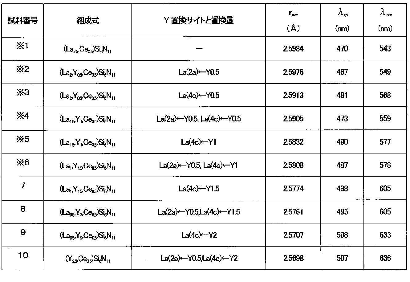
表2および図4から、Y3+の置換量が増加すると発光波長が大きくなる傾向が読みとれる。また、励起ピーク波長も、発光波長の長波長化に伴い大きくなっていることがわかる。発光波長が600nm以上を示す赤色発光となる試料7から試料10の組成系においては、励起波長のピークが490nm以上の緑色領域となることがわかる。また、図5から明らかなように、Y3+の置換量が増加するほどa軸の格子定数が減少し、c軸の格子定数が増加するのがわかる。また表2および図6から明らかなように、Y3+の置換量が増加するほどCe-N間の平均配位距離raveが減少し、raveの減少と共に、発光波長および励起波長ともに増化することがわかる。
Eu2+の発光寿命は、Ce3+の発光寿命と比較して、とても長い。発光寿命は、Eu2+Ce3+それぞれの4f-5d遷移の遷移確率と相関があり、発光寿命が長いほど遷移確率が低いといえる。つまり、Eu2+の4f-5d遷移の励起確率は、Ce3+の4f-5d遷移の励起確率と比較して、とても低いといえる。しかしながら、Eu2+は5d励起準位が母体材料((La,Y)3Si6N11)のコンダクションバンドと重なりやすい。よって、Eu2+の4f基底準位と母体材料のコンダクションバンドとの間で効率的にエネルギーを吸収することが可能となる。この吸収エネルギーは、青色光領域のエネルギーに相当する。またEu2+は4f軌道に7つの電子があり、それぞれの電子のエネルギー準位が幅を有するため、励起波長はブロードとなる。つまりEu2+を発光中心として用いた赤色蛍光体の励起波長は、青色領域をピークとしたブロードな励起波長となる。そのため、Eu2+を発光中心として用いた赤色蛍光体を使用した光源では、励起光源には最も吸収効率の高くなる青色光が用いられている。
一方、Ce3+を発光中心として用いた蛍光体の場合では、5d励起準位が母体材料のコンダクションバンドと重なりにくい。よって、4f基底準位と母体材料のコンダクションバンドとの間でのエネルギー吸収は期待できない。そのため、4f-5d遷移がエネルギー吸収の主体となる。
本発明者らは、上述の検討の結果により、Ce3+を用いた赤色蛍光体の場合には、4f-5d遷移間のエネルギー差が緑色光領域のエネルギー差になることを明らかにした。したがって、Ce3+を用いた赤色蛍光体の場合には、励起光源に青色光を用いるよりも緑色光を用いた方が、蛍光体の吸収効率が高くなる。よって緑色光を用いることにより、光出力を高めることができる。さらに、青色光から赤色光へ変換する従来の方式と比較して、緑色光から赤色光へ変換する本願の方式の方が、エネルギー変換ロス(ストークス・ロス)を小さくできるため、より高出力の光を放射することが可能となる。
<実施形態1の蛍光体>
以上の結果から、本発明者らは、本開示の一実施形態の蛍光体として、化学組成CexYyLa3-x-ySi6N11を有する結晶相を含有し、0<x≦0.6であり、(1.5-x)≦y≦(3-x)である、新規赤色蛍光体に到達した。以下に、実施形態1の蛍光体について、より詳しく説明する。
以上の結果から、本発明者らは、本開示の一実施形態の蛍光体として、化学組成CexYyLa3-x-ySi6N11を有する結晶相を含有し、0<x≦0.6であり、(1.5-x)≦y≦(3-x)である、新規赤色蛍光体に到達した。以下に、実施形態1の蛍光体について、より詳しく説明する。
上記のとおり、実施形態1の蛍光体の化学組成において、xは、0<x≦0.6を満たす。xは0より大きいので、Ceによる発光を得ることができる。xは、発光強度増大の観点から、望ましくは0.0003以上、より望ましくは0.015以上である。蛍光体が発光し得る限りxの最大値に特に制限はない。しかし、xが大きくなりすぎる場合には、濃度消光により発光強度が低下する。そのため、xを0.6以下とすることにより、発光強度の低下を抑制できる。また、xは、発光強度増大の観点から、望ましくは0.3以下、より望ましくは0.15以下である。
実施形態1の蛍光体では、発光波長および励起波長の長波長化の観点から、YによるLaの置換量が大きいことが望ましい。したがって、本実施形態の蛍光体の化学組成において、xおよびyは、(1.5-0.5x)≦y≦(3-x)を満たすことが望ましく、1.5≦y≦(3-x)を満たすことがより望ましい。
実施形態1の蛍光体は、波長600nm以上660nm以下の範囲内に発光スペクトルのピークを有する。実施形態1の蛍光体は、例えば、波長605nm以上の発光スペクトルのピークを有してもよい。実施形態1の蛍光体は、例えば、波長640nm以下の発光スペクトルのピークを有してもよく、波長636nm下の発光スペクトルピークを有してもよい。
実施形態1の蛍光体は、波長480nm以上550nm以下の範囲内に励起スペクトルのピークを有する。実施形態1の蛍光体は、例えば、波長490nm以上の励起スペクトルのピークを有してもよく、波長495nm以上の励起スペクトルピークを有してもよい。実施形態1の蛍光体は、例えば、波長530nm以下の励起スペクトルのピークを有してもよく、波長508nm下の励起スペクトルピークを有してもよい。
実施形態1の蛍光体は、波長480nm以上550nm以下の範囲の励起スペクトルのピークを第一の励起スペクトルのピークとした場合に、波長350nm以上480nm未満の範囲内に、第二の励起スペクトルのピークをさらに有してもよい。第一または第二の励起スペクトルのピークは、励起スペクトルの最大ピークであってもよい。
また、実施形態1の蛍光体の結晶相の1/e発光寿命は、100ns以下の値を示してもよい。発光寿命は、輝度飽和特性に影響する。従来の赤色蛍光体であるCASN:EuなどのEuを含む蛍光体は、Ceを含む蛍光体と比較して発光寿命が長い。そのため、Euを含む蛍光体は、高出力励起時に量子効率が低下することで輝度飽和しやすい。したがって、Ceを発光中心とした実施形態1の蛍光体は、従来の赤色蛍光体と比較して、高出力時でも量子効率が高い赤色蛍光体として有望である。
また、実施形態1の蛍光体における母体材料の結晶が正方晶(テトラゴナル)であってよい。換言すると、実施形態1の蛍光体における化学組成CexYyLa3-x-ySi6N11を有する結晶相が、正方晶(テトラゴナル)の結晶構造を有してもよい。また、当該結晶相は、一般式La3Si6N11で表される結晶と、ほとんど同じ結晶構造を有してもよい。
実施形態1の蛍光体の結晶相は、CeがLa3Si6N11の結晶構造におけるLa(2a)サイトの少なくとも一部を置換している結晶構造を有してもよい。また実施形態1の蛍光体の結晶相は、YがLa3Si6N11の結晶構造におけるLa(4c)サイトの少なくとも一部を置換している結晶構造を有してもよく、YがLa3Si6N11の結晶構造におけるLa(4c)サイトの過半数を置換している結晶構造を有してもよい。
La3Si6N11の結晶構造におけるLaの配位状態には、図7に示すように、La(2a)サイトと、La(4c)サイトとの2種類が存在する。La(2a)サイトは対称性が高く、La(4c)サイトは対称性が低い。例えば、対称性が高いLa(2a)サイトのLaがイオン半径の大きいCeで置換された場合、第一原理計算から求めた生成エンタルピーが約48meV程度低く、熱力学的に安定である。この観点から、実施形態1の蛍光体の結晶相は、CeがLa3Si6N11の結晶構造におけるLa(2a)サイトの少なくとも一部を置換している結晶構造を有することが望ましい。また、例えば、対称性が低いLa(4c)サイトのLaがYで置換された場合、格子ひずみが大きいためCeの5d軌道の分裂が大きくなる。よって、4f-5d軌道間のエネルギー差が減少するため、励起波長および発光波長を長波長側へシフトさせることができる。この観点から、実施形態1の蛍光体の結晶相は、YがLa3Si6N11の結晶構造におけるLa(4c)サイトの少なくとも一部を置換している結晶構造を有することが望ましい。さらに、YがLa3Si6N11の結晶構造におけるLa(4c)サイトの過半数を置換している結晶構造を有することがより望ましい。
<蛍光体の製造方法>
以下、実施形態1の蛍光体の製造方法について説明する。
以下、実施形態1の蛍光体の製造方法について説明する。
原料としては、例えば、Ce、La、SiおよびYをそれぞれ含有する化合物を用いてもよいし、Ce、La、SiおよびYそれぞれの単体を用いてもよい。化合物としては、窒素雰囲気下での焼成により窒化物になる化合物、高純度(純度99%以上)の窒化物、金属合金、などを用いることができる。また、反応を促進するために、フッ化物(フッ化アンモニウム等)を少量添加してもよい。
例えば、CexYyLa3-x-ySi6N11(0<x≦0.6、(1.5-x)≦y≦(3-x)で表される化学組成比となるように、Ce化合物、La化合物、Si化合物およびY化合物を用意してもよい。ここで、Si化合物に代えてSi単体を用意してもよい。具体的な原料としては、例えば、CeF3粉末、LaN粉末、Si3N4粉末および、YN粉末を用いてもよい。ここで、CeF3粉末に代えてCeN粉末を用いてもよい。また、Si3N4粉末に代えてSi単体の粉末を用いてもよい。また、LaN粉末は、理論値よりも24%程度過剰に用意してもよい。LaNは焼成時に分解しやすいため、原料配合時に過剰に仕込むことで、副生成物であるLaSi3N5結晶の生成を抑制できる。
実施形態1の蛍光体の製造は、上記の原料を混合し、焼成して行う。原料の混合方法は、溶液中での湿式混合でも、乾燥粉体の乾式混合でもよい。工業的に通常用いられるボールミル、媒体撹拌ミル、遊星ミル、振動ミル、ジェットミル、V型混合機、攪拌機等を用いることができる。焼成は、窒素により加圧した雰囲気中において1500~2000℃の温度範囲で1~50時間程度行う。このときの圧力は、通常3気圧以上、望ましくは4気圧以上、より望ましくは8気圧以上である。焼成後の蛍光体は、例えば、濃度10%の硝酸溶液中で1時間洗浄してもよい。得られた蛍光体粉末を、ボールミルやジェットミルなどを用いて再度粉砕し、さらに必要に応じて洗浄または分級することにより、蛍光体粉末の粒度分布や流動性を調整してもよい。
<蛍光体を用いた発光装置>
実施形態1の蛍光体は、発光装置に利用されうる。本実施形態における発光装置は、励起光源と、第一の蛍光体と、を少なくとも備える。励起光源は、波長600nm以下の光を発する。第一の蛍光体は、励起光源の発する光を照射され、励起光源の発する光よりも長波長の蛍光を発する。第一の蛍光体は、例えば、実施形態1で説明した何れかの蛍光体である。以上の構成によれば、高出力時においても量子効率の高い発光装置を構成することができる。
実施形態1の蛍光体は、発光装置に利用されうる。本実施形態における発光装置は、励起光源と、第一の蛍光体と、を少なくとも備える。励起光源は、波長600nm以下の光を発する。第一の蛍光体は、励起光源の発する光を照射され、励起光源の発する光よりも長波長の蛍光を発する。第一の蛍光体は、例えば、実施形態1で説明した何れかの蛍光体である。以上の構成によれば、高出力時においても量子効率の高い発光装置を構成することができる。
また、励起光源の発する光は、波長480nm以上600nm以下であってもよい。実施形態1の蛍光体は、典型的には、波長480nm以上550nm以下の範囲内に励起スペクトルのピークを有するため、上記波長範囲の光を発する励起光源を用いることにより、効率的に励起することができる。また、励起光源の発する光は、波長200nm以上480nm以下の光を含んでいてもよいし、波長420nm以上480nm以下の光を含んでいてもよい。実施形態1の蛍光体は、波長480nm以下においても励起光を吸収し得る。また、波長200nm以下の光は、空気による吸収で減衰するため、波長200nm以上の光を発する励起光源が望ましい。なお、上記の励起光源としては、例えば、LEDまたはLDが挙げられる。
また、本実施形態における発光装置は、波長500nm以上600nm以下の範囲内に発光スペクトルのピークを有する第二の蛍光体をさらに含んでもよい。すなわち、発光装置は、第一の蛍光体と第二の蛍光体の組合せを含んでよい。第二の蛍光体は、励起光源が発する光を照射されることで、励起光源が発する光よりも長波長の蛍光を発する。第二の蛍光体としては、化学組成Y3Al5O12:Ce(YAG:Ce)の結晶相を含有する蛍光体や、化学組成La3Si6N11:Ce(LSN:Ce)を有する結晶相を含有する蛍光体などを用いてもよい。
また、第二の蛍光体は、例えば、黄色光を発する蛍光体であってもよい。発光装置は、さらに、緑色光を発する第三の蛍光体を含んでもよい。すなわち、発光装置は、第一の蛍光体と、黄色光を発する第二の蛍光体と、緑色光を発する第三の蛍光体との組合せを含んでよい。第三の蛍光体は、励起光源が発する光を照射されることで、励起光源が発する光よりも長波長の蛍光を発する。第三の蛍光体としては、化学組成Lu3Al5O12:Ce(LuAG:Ce)の結晶相を含有する蛍光体や、化学組成Y3(Al,Ga)5N12:Ce(YAGG:Ce)を有する結晶相を含有する蛍光体などを用いてもよい。なお、第二の蛍光体および/または第三の蛍光体が発する光を利用して、実施形態1の蛍光体を励起してもよい。なお、緑色光とは、CIE色度座標値において、(0.1≦x≦0.4、0.5≦y≦0.8)の範囲に位置する光をいう。また、黄色光とは、CIE色度座標値において、(0.4≦x≦0.6、0.4≦y≦0.6)の範囲に位置する光をいう。
実施形態1の蛍光体を含む発光装置における、励起光源および第二、第三の蛍光体は、発光装置の用途に応じて、上述の範囲内で自由に選択することができる。したがって、実施形態1の蛍光体を含む発光装置は、赤色発光装置のみならず、白色発光装置などとしても有用である。具体的には、青色光を発する励起光源と、黄色光を発する蛍光体と、本実施形態の赤色蛍光体と、を組み合わせることで、演色性の高い高出力の発光装置や電球色に発光する高出力の発光装置を実現できる。
[実施形態2]
実施形態2では、本開示の発光装置の一例として、発光素子としてのLEDチップを光源とするLED発光装置について説明する。図10は、実施形態2のLED発光装置の一実施形態を示す模式的な断面図である。図10に示すように、LED発光装置10は、蛍光体11と、LEDチップ15と、LED封止体24と、を備える。また、LED発光装置10は支持体23を備えてもよい。支持体23は、LEDチップ15を支持する。本実施形態では、LED発光装置10は、面実装が可能な構造を備えているため、支持体23は基板である。
実施形態2では、本開示の発光装置の一例として、発光素子としてのLEDチップを光源とするLED発光装置について説明する。図10は、実施形態2のLED発光装置の一実施形態を示す模式的な断面図である。図10に示すように、LED発光装置10は、蛍光体11と、LEDチップ15と、LED封止体24と、を備える。また、LED発光装置10は支持体23を備えてもよい。支持体23は、LEDチップ15を支持する。本実施形態では、LED発光装置10は、面実装が可能な構造を備えているため、支持体23は基板である。
本実施形態は高輝度LED発光装置に用いることができる。例えば、LEDチップ15で発生した熱を効率的に外部へ放熱することができるよう、支持体23は高い熱伝導率を有している。例えば、アルミナや窒化アルミニウムなどからなるセラミック基板を支持体23として用いることができる。
LEDチップ15には、例えば、紫外から黄色領域で発光するものが用いられ、波長200nm以上600nm以下の範囲内に発光スペクトルのピークを有するものが用いられる。LEDチップ15として、具体的には、黄色LEDチップ、緑色LEDチップ、青色LEDチップ、青紫色LEDチップ、近紫外LEDチップ、紫外LEDチップ等が用いられる。LEDチップ15は、支持体23上において、出射面15aが支持体23と接する面とならないように、半田27などによって支持体23に固定されている。また、LEDチップ15はボンディングワイヤ21によって支持体23に設けられた電極22に電気的に接続されている。LEDチップ15は、LED封止体24で覆われている。
LED封止体24には、例えばシリコーン樹脂が使用されている。蛍光体11が、LED封止体24中に分散している。シリコーン樹脂には、半導体発光素子の封止樹脂として用いられる種々の化学式で規定される構造のシリコーン樹脂を用いることができる。シリコーン樹脂は、例えば、耐変色性が高いジメチルシリコーンを含んでいる。また、耐熱性の高いメチルフェニルシリコーン等もシリコーン樹脂として用いることができる。シリコーン樹脂は1種類の化学式で規定されるシロキサン結合による主骨格を持つ単独重合体であってもよい。また、2種類以上の化学式で規定されるシロキサン結合を有する構造単位を含む共重合体や2種類以上のシリコーンポリマーのアロイであってもよい。
本実施形態では、LED封止体24中のシリコーン樹脂は硬化後の状態にある。したがって、LED封止体24も硬化した状態にある。以下において説明するように、LED封止体24は、未硬化のシリコーン樹脂を用いて作製することができる。シリコーン樹脂は、主剤および硬化剤を混合することにより硬化が促進される2液型であることが一般的である。しかし、熱硬化型、あるいは、光などのエネルギーを照射することによって硬化するエネルギー硬化型のシリコーン樹脂を用いることもできる。なお、LED封止体24には、シリコーン樹脂以外のものを使用してもよい。例えば、ガラス、エポキシ樹脂、ZnOで構成される無機材料等を用いてもよい。また、蛍光体11は、LED封止体24中に分散させずに、LED封止体24上に蛍光体板の形態で配置してもよい。
上述した例では、LEDチップはワイヤボンディングされていたが、本実施形態で用いられるLEDチップは他の構成であってもよい。すなわち、本実施形態で用いられるLEDチップは、フェイスアップで実装されるものであっても、フリップチップで実装されるものであってもよい。また本実施形態で用いられるLEDチップは、一般的な極性面(c面)の成長面を有する窒化物半導体から形成される発光層を備えるものであってもよい。
<蛍光体の概要>
蛍光体11は、LEDチップ15から出射される近紫外から黄色領域の光(例えば、近紫外光)のうち、一部の波長成分、あるいは、すべての波長成分を吸収し、蛍光を発する。吸収する光の波長および蛍光の波長は、蛍光体11に含まれる蛍光材料の種類によって決まる。蛍光体11は、光の混色により白色光が作り出されるように、複数の異なる色の蛍光体を含む混合蛍光体であってもよい。蛍光体11は、緑色蛍光体および赤色蛍光体の混合蛍光体であってもよい。赤色蛍光体としては、実施形態1の蛍光体が用いられる。
蛍光体11は、LEDチップ15から出射される近紫外から黄色領域の光(例えば、近紫外光)のうち、一部の波長成分、あるいは、すべての波長成分を吸収し、蛍光を発する。吸収する光の波長および蛍光の波長は、蛍光体11に含まれる蛍光材料の種類によって決まる。蛍光体11は、光の混色により白色光が作り出されるように、複数の異なる色の蛍光体を含む混合蛍光体であってもよい。蛍光体11は、緑色蛍光体および赤色蛍光体の混合蛍光体であってもよい。赤色蛍光体としては、実施形態1の蛍光体が用いられる。
緑色蛍光体としては、例えば、MII
2MgSi2O7:Eu2+(MII=Ba,SrおよびCaから選ばれる少なくとも1種)、SrSi5AlO2N7:Eu2+、SrSi2O2N2:Eu2+、BaAl2O4:Eu2+、BaZrSi3O9:Eu2+、MII
2SiO4:Eu2+(MII=Ba,SrおよびCaから選ばれる少なくとも1種)、BaSi3O4N2:Eu2+、Ca8Mg(SiO4)4Cl2:Eu2+、Ca3SiO4Cl2:Eu2+、β-SiAlON:Eu2+などの蛍光体を用いることができる。
別の態様として、蛍光体11は、黄色蛍光体および赤色蛍光体の混合蛍光体であってもよい。赤色蛍光体としては、実施形態1の蛍光体が用いられる。黄色蛍光体としては、例えば、Y3Al5O12:Ce3+、CaSi2O2N2:Eu2+、(Ba,Sr)Si2O2N2:Eu2+、Ca3Sc2Si3O12:Ce3+、CaSc2O4:Ce3+、α-SiAlON:Eu2+、La3Si6N11:Ce3+などの蛍光体を用いることができる。
また、蛍光体11の粒子径は、例えば、それぞれ1μm以上80μm以下である。本明細書において、粒子径とは、顕微鏡法による円相当径で表したものをいう。
蛍光体11は、例えば、封止体100重量部に対して、3重量部以上70重量部以下の割合でLED封止体24に含まれている。蛍光体11の含有量が3重量部よりも少ない場合、十分な強度の蛍光が得られないため、所望の波長の光を発光するLED発光装置10を実現できなくなる場合がある。蛍光体11に用いる各色に発光する蛍光体の重量比は、所望する白色光の色調と、それぞれの蛍光体の発光強度に応じて適宜決定することができる。なお、蛍光体11を、実施形態1の赤色蛍光体のみにすることによって、あるいは、他の色の蛍光体と組み合わせることによって、LED発光装置を、白色以外の色を発するLED発光装置として構成することもできる。
実施形態1の赤色蛍光体以外の上記の蛍光体は、公知方法に従って製造することができる。具体的には、酸化物蛍光体を作製する場合、原料としては、水酸化物、蓚酸塩、硝酸塩など、焼成により酸化物になる化合物、または、酸化物を用いることができる。ここで、反応を促進するために、フッ化物(例えば、フッ化カルシウム等)や塩化物(例えば、塩化カルシウム等)を少量添加することができる。蛍光体の製造は、上記の原料を混合し、焼成して行う。
原料の混合方法としては、溶媒中での湿式混合でも、乾燥粉体の乾式混合でもよい。工業的に通常用いられるボールミル、媒体撹拌ミル、遊星ミル、振動ミル、ジェットミル、V型混合機、攪拌機等を用いることができる。蛍光体原料の焼成は、大気中または還元性雰囲気下において、1100~1700℃の温度範囲で1~50時間程度行う。焼成に用いる炉は、工業的に通常用いられる炉を用いることができる。例えば、プッシャー炉等の連続式またはバッチ式の電気炉やガス炉、または、プラズマ焼結(SPS)や熱間静水圧加圧焼結(HIP)等の加圧焼成炉を用いることができる。得られた蛍光体粉末を、ボールミルやジェットミルなどを用いて再度粉砕し、さらに必要に応じて洗浄または分級することにより、蛍光体粉末の粒度分布や流動性を調整することができる。
[実施形態3]
実施形態3では、本開示の発光装置の一例として、発光素子としてのLDを光源とするLD発光装置について説明する。図11は、実施形態3に係るLD発光装置60の概略構成を示している。LD発光装置60は、LD素子58と、波長変換部材61と、を備える。波長変換部材61は、蛍光体を含む。蛍光体は、LD素子58からの出射光を、より長波長の光に波長変換する。
実施形態3では、本開示の発光装置の一例として、発光素子としてのLDを光源とするLD発光装置について説明する。図11は、実施形態3に係るLD発光装置60の概略構成を示している。LD発光装置60は、LD素子58と、波長変換部材61と、を備える。波長変換部材61は、蛍光体を含む。蛍光体は、LD素子58からの出射光を、より長波長の光に波長変換する。
LD素子58は、LEDよりも高い光パワー密度の光を出射することができる。よって、LD素子58の使用により高出力のLD発光装置60を構成することができる。LD素子58から蛍光体に照射される光パワー密度は、LD発光装置60の高出力化の観点から、例えば、0.5W/mm2以上である。また、蛍光体に照射される光パワー密度は、2W/mm2以上であってもよく、3W/mm2以上であってもよく、10W/mm2以上であってよい。一方で、蛍光体に照射される光パワー密度が高すぎると、蛍光体からの発熱量が増大して、LD発光装置60に悪影響を及ぼすおそれがある。よって、蛍光体に照射される光パワー密度は、150W/mm2以下であってもよく、100W/mm2以下であってもよく、50W/mm2以下であってもよく、20W/mm2以下であってもよい。
LD素子58には、蛍光体を励起可能な波長の光を出射するものを特に制限なく使用することができる。例えば、青紫光を出射するLD素子、青色光を出射するLD素子、緑色光を出射するLD素子、黄色光を出射するLD素子等を使用することができる。本実施形態では、LD素子58が、青色光を出射する場合について説明する。本明細書において、青色光とは、ピーク波長が420nm以上480nm未満の光をいう。一般に、青色光を出射するLD素子58は、紫外光を出射するLD素子よりも発光効率が高く、発光ピーク波長が445nmの場合には、最も発光効率が高くなる。LD素子58の発光ピーク波長は、425nm以上であってもよく、430nm以上であってもよい。一方で、LD素子58の発光ピーク波長は、475nm以下であってもよく、470nm以下であってもよい。
LD素子58は、1つのLDから構成されたものであってもよく、複数のLDを光学的に結合させたものであってもよい。LD素子58は、例えば、非極性面または半極性面である成長面を有する窒化物半導体から形成される発光層を備えてもよい。
波長変換部材61の蛍光体は、実施形態1の赤色蛍光体を含む。波長変換部材61は、発光装置の所望の発光色に応じて、実施形態1の赤色蛍光体以外の蛍光体をさらに含んでいてもよい。例えば、波長変換部材61が、黄色蛍光体および緑色蛍光体をさらに含む場合には、LD発光装置60を白色発光装置として構成することができる。黄色蛍光体および緑色蛍光体としては、実施形態2で例示したものを使用することができる。波長変換部材61は、複数種の蛍光体が混合された一層の波長変換層であってもよく、単一種あるいは複数種の蛍光体を含む波長変換層が少なくとも2層以上積層されたものであってもよい。本実施形態では、特に、赤色蛍光体12で構成される第1の蛍光体層62と、黄色蛍光体13で構成される第2の蛍光体層63とを積層した構成を有する波長変換部材61が用いられる場合について説明する。
第1の蛍光体層62、第2の蛍光体層63は、それぞれ、バインダー68,69を用いて構成されている。バインダー68,69は、例えば、樹脂、ガラスまたは透明結晶などの媒体である。バインダー68,69は、同じ材質であってもよく、異なる材質であってもよい。なお、各蛍光体層は、蛍光体粒子のみで構成されていてもよい。
波長変換部材61とLD素子58との間には、LD素子58の光を第2の蛍光体層63に導く入射光学系59が設けられていてもよい。入射光学系59は、例えば、レンズ、ミラー、または光ファイバーなどを備えている。
次に、LD発光装置60の動作について説明する。LD素子58から出射された青色光は、入射光学系59を通り、波長変換部材61の第2の蛍光体層63に入射する。この入射光により、第2の蛍光体層63の複数の黄色蛍光体13が励起されて黄色光を出射する。また、第2の蛍光体層63で吸収されずに透過したLD素子58から出射された青色光は、第1の蛍光体層62に入射する。この入射により、第1の蛍光体層62の複数の赤色蛍光体12が励起され赤色光を出射する。また、第2の蛍光体層63から放射された黄色光が、第1の蛍光体層62に入射する。この入射光の一部により、第1の蛍光体層62の複数の赤色蛍光体12が励起され赤色光を出射してもよい。また、第1の蛍光体層62でも第2の蛍光体層63でも吸収されずに透過したLD素子58から出射された青色光は、外部へと放射される。これらの赤色光、黄色光、および青色光が混合して、白色光となる。
なお、各蛍光体層の厚みは、LD素子58から出射された青色光が第1の蛍光体層62を透過しないように調整してもよい。また、第2の蛍光体層63から放射された黄色光が、第1の蛍光体層62を透過しないように調整してもよい。この場合には、外部へ赤色光のみが放射される。別の態様として、第2の蛍光体層63で用いている黄色蛍光体13に代えて、実施形態2で説明した緑色蛍光体を用いてもよい。
[実施形態4]
実施形態4では、本開示の発光装置の一例として、発光素子としてのLDを光源とするLD発光装置について説明する。図12は、実施形態4に係るLD発光装置80の概略構成を示している。実施形態3と同一の部材については、同一の符号を付してその説明を省略する。LD発光装置80は、LD素子58と、波長変換部材81と、を備える。
実施形態4では、本開示の発光装置の一例として、発光素子としてのLDを光源とするLD発光装置について説明する。図12は、実施形態4に係るLD発光装置80の概略構成を示している。実施形態3と同一の部材については、同一の符号を付してその説明を省略する。LD発光装置80は、LD素子58と、波長変換部材81と、を備える。
波長変換部材81は、蛍光体を含む。蛍光体は、LD素子58からの出射光を、より長波長の光に波長変換する。波長変換部材81の蛍光体は、赤色蛍光体12と、黄色蛍光体13および緑色蛍光体14からなる群より選ばれる少なくとも1種とが混合された波長変換層を有する。赤色蛍光体12としては、実施形態1の蛍光体が用いられる。黄色蛍光体および緑色蛍光体としては、実施形態2で例示したものを使用することができる。本実施形態では、特に、波長変換部材81が、赤色蛍光体12、黄色蛍光体13、および緑色蛍光体14の3種を混合して形成した蛍光体層である場合を説明する。3種の蛍光体の混合比率は、所望の白色光の色調や、各蛍光体の発光強度などに応じて、適宜調整することが可能である。
波長変換部材81である蛍光体層は、バインダー68を用いて構成されている。バインダー68は、例えば、樹脂、ガラス、または透明結晶などの媒体である。バインダー68は、単一の材質であってもよく、場所により異なる材質であってもよい。なお、蛍光体層は、蛍光体粒子のみで構成されていてもよい。
LD素子58から出射された青色光は、入射光学系59を通り、波長変換部材81中の赤色蛍光体12、黄色蛍光体13、および緑色蛍光体14により、それぞれ赤色光、黄色光、緑色光に変換される。蛍光体で吸収されなかったLD素子58から出射された青色光と、赤色蛍光体12、黄色蛍光体13および緑色蛍光体14によりそれぞれ変換された赤色光、黄色光、緑色光とを混合して、白色光となる。なお、赤色蛍光体12は、緑色蛍光体14により出射された緑色光の一部の入射により励起されて、赤色光を出射する。
上述のように、実施形態2~4の発光装置によれば、実施形態1の赤色蛍光体を用いるため、高出力時において従来よりも量子効率を向上させることができる。さらに、白色発光装置として構成した場合には、高い演色性および色再現性を実現できる。
[実施形態5]
実施形態5では、本開示の照明装置の一例について説明する。図13は、実施形態5に係る照明装置120の概略構成を示している。照明装置120は、光源121と、光源121が発する光を前方に導く出射光学系122と、を備える。光源からの発光色を調整するために、光源からの光を吸収または反射する波長カットフィルター123を設けてもよい。光源121は、実施形態1の赤色蛍光体を含む。また、光源121は、実施形態2~4の発光装置10、60または80であってもよい。出射光学系122は、例えば、リフレクタであってもよい。出射光学系122は、例えば、AlまたはAgなどの金属膜、または、表面に保護膜が形成されたAl膜を有してもよい。
実施形態5では、本開示の照明装置の一例について説明する。図13は、実施形態5に係る照明装置120の概略構成を示している。照明装置120は、光源121と、光源121が発する光を前方に導く出射光学系122と、を備える。光源からの発光色を調整するために、光源からの光を吸収または反射する波長カットフィルター123を設けてもよい。光源121は、実施形態1の赤色蛍光体を含む。また、光源121は、実施形態2~4の発光装置10、60または80であってもよい。出射光学系122は、例えば、リフレクタであってもよい。出射光学系122は、例えば、AlまたはAgなどの金属膜、または、表面に保護膜が形成されたAl膜を有してもよい。
実施形態5の照明装置によれば、実施形態1の赤色蛍光体を用いるため、高出力時において従来の照明装置よりも量子効率を向上させることができる。さらに、白色照明装置として構成した場合には、高い演色性および色再現性を実現できる。
[実施形態6]
実施形態6では、本開示の照明装置の一例として、光ファイバーを用いた照明装置について説明する。図14は、実施形態6に係る照明装置130の概略構成を示している。照明装置130は、LD素子58と、入射光学系59と、光ファイバー132と、波長変換部材131と、出射光学系122と、を備える。
実施形態6では、本開示の照明装置の一例として、光ファイバーを用いた照明装置について説明する。図14は、実施形態6に係る照明装置130の概略構成を示している。照明装置130は、LD素子58と、入射光学系59と、光ファイバー132と、波長変換部材131と、出射光学系122と、を備える。
LD素子58が発する光は、入射光学系59を通り、光ファイバー132へと導かれる。光ファイバー132は、その光を出射部へと導く。出射部は、例えば、波長変換部材131と、出射光学系122と、を備える。波長変換部材131は、実施形態1の赤色蛍光体を含む。また、波長変換部材131は、実施形態3~4の波長変換部材61または81であってもよい。なお、波長変換部材131は、図14のように光ファイバー132よりも出射側に位置してもよいが、光ファイバー132よりも入射側(例えば、LD素子58と入射光学系59との間、または、入射光学系59と光ファイバー132との間)に位置してもよい。
実施形態6の照明装置によれば、光ファイバーを用いることで、光の照射方向を簡便に変更することができる。
また、実施形態1の赤色蛍光体を用いるため、高出力時において従来の照明装置よりも量子効率を向上させることができる。さらに、白色照明装置として構成した場合には、高い演色性および色再現性を実現できる。
[実施形態7]
実施形態7では、本開示の照明装置の応用例として、照明装置を備えた車両について説明する。図15は、実施形態7に係る車両140の概略構成を示している。車両140は、実施形態5の照明装置120である車両用ヘッドランプと、電力供給源141と、を備える。また、車両140は、エンジン等の駆動源によって回転駆動され、電力を発生する発電機142を有してもよい。発電機142が生成した電力は、電力供給源141に蓄えられてもよい。電力供給源141は、充放電が可能な2次電池であってもよい。照明装置120は、電力供給源141からの電力によって点灯する。車両140は、例えば、自動車、2輪車、または特殊車両である。また、車両140は、エンジン車、電気車、またはハイブリッド車であってもよい。
実施形態7では、本開示の照明装置の応用例として、照明装置を備えた車両について説明する。図15は、実施形態7に係る車両140の概略構成を示している。車両140は、実施形態5の照明装置120である車両用ヘッドランプと、電力供給源141と、を備える。また、車両140は、エンジン等の駆動源によって回転駆動され、電力を発生する発電機142を有してもよい。発電機142が生成した電力は、電力供給源141に蓄えられてもよい。電力供給源141は、充放電が可能な2次電池であってもよい。照明装置120は、電力供給源141からの電力によって点灯する。車両140は、例えば、自動車、2輪車、または特殊車両である。また、車両140は、エンジン車、電気車、またはハイブリッド車であってもよい。
実施形態7の車両によれば、実施形態1の赤色蛍光体を含む車両用ヘッドランプを用いるため、高出力時において従来よりも前方を明るく照らすことができる。さらに、白色照明装置として構成した場合には、高い演色性および色再現性を実現できる。
本開示の蛍光体は、発光装置などとして有用である。本開示の蛍光体は、例えば、シーリングライト等の一般照明装置、スポットライト、スタジアム用照明、スタジオ用照明等の特殊照明装置、ヘッドランプ等の車両用照明装置、プロジェクター、ヘッドアップディスプレイ等の投影装置、内視鏡用ライト、デジタルカメラ、携帯電話機、スマートフォンなどの撮像装置、パーソナルコンピュータ(PC)用モニター、ノート型パーソナルコンピュータ、テレビ、携帯情報端末(PDX)、スマートフォン、タブレットPC、携帯電話などの液晶ディスプレイ装置等における光源として用いることができる。
10 LED発光装置
11 蛍光体
12 赤色蛍光体
13 黄色蛍光体
14 緑色蛍光体
15 LEDチップ
21 ボンディングワイヤ
22 電極
23 支持体
24 LED封止体
27 半田
58 LD素子
59 入射光学系
60 LD発光装置
61 波長変換部材
62 第1の蛍光体層
63 第2の蛍光体層
68 バインダー
69 バインダー
80 LD発光装置
81 波長変換部材
120 照明装置
121 光源
122 出射光学系
123 波長カットフィルター
130 照明装置
131 波長変換部材
132 光ファイバー
140 車両
141 電力供給源
142 発電機
11 蛍光体
12 赤色蛍光体
13 黄色蛍光体
14 緑色蛍光体
15 LEDチップ
21 ボンディングワイヤ
22 電極
23 支持体
24 LED封止体
27 半田
58 LD素子
59 入射光学系
60 LD発光装置
61 波長変換部材
62 第1の蛍光体層
63 第2の蛍光体層
68 バインダー
69 バインダー
80 LD発光装置
81 波長変換部材
120 照明装置
121 光源
122 出射光学系
123 波長カットフィルター
130 照明装置
131 波長変換部材
132 光ファイバー
140 車両
141 電力供給源
142 発電機
Claims (15)
- 化学組成CexYyLa3-x-ySi6N11を有する結晶相を含有し、
0<x≦0.6であり、
(1.5-x)≦y≦(3-x)であり、
波長600nm以上660nm以下の範囲内に発光スペクトルのピークを有し、
波長480nm以上550nm以下の範囲内に励起スペクトルの第一のピークを有する、
蛍光体。 - 前記xおよび前記yは、(1.5-0.5x)≦y≦(3-x)を満たす、
請求項1に記載の蛍光体。 - 前記xおよび前記yは、1.5≦y≦(3-x)を満たす、
請求項2に記載の蛍光体。 - 前記結晶相が正方晶(テトラゴナル)の結晶構造を有する、
請求項1から3のいずれか1項に記載の蛍光体。 - 波長350nm以上480nm未満の範囲内に前記励起スペクトルの第二のピークを有する、
請求項1から4のいずれか1項に記載の蛍光体。 - 前記結晶相の1/e発光寿命が100ns以下である、
請求項1から5のいずれか1項に記載の蛍光体。 - 前記結晶相は、CeがLa3Si6N11の結晶構造におけるLa(2a)サイトの少なくとも一部を置換している結晶構造を有する、
請求項1から6のいずれか1項に記載の蛍光体。 - 前記結晶相は、YがLa3Si6N11の結晶構造におけるLa(4c)サイトの少なくとも一部を置換している結晶構造を有する、
請求項1から7のいずれか1項に記載の蛍光体。 - 前記結晶相は、YがLa3Si6N11の結晶構造におけるLa(4c)サイトの過半数を置換している結晶構造を有する、
請求項8に記載の蛍光体。 - 波長600nm以下の光を発する励起光源と、
請求項1から9のいずれか1項に記載の蛍光体である第一の蛍光体と、
を備え、
前記第一の蛍光体は、前記励起光源の発する光を照射され、前記光よりも長波長の蛍光を発する、
発光装置。 - 前記励起光源は、波長480nm以上600nm以下の光を発する、
請求項10に記載の発光装置。 - 前記励起光源は、波長420nm以上480nm以下の光を発する、
請求項10に記載の発光装置。 - 前記励起光源は、LEDまたはLDである、
請求項10から12のいずれか1項に記載の発光装置。 - 前記励起光源の発する光を照射され、前記光よりも長波長の蛍光を発する、第二の蛍光体をさらに備え、
前記第二の蛍光体は、波長480nm以上600nm未満の範囲内に発光スペクトルのピークを有する、
請求項10から13のいずれか1項に記載の発光装置。 - 前記第二の蛍光体は、黄色光を発する蛍光体であり、
前記励起光源の発する光を照射され、前記光よりも長波長の蛍光を発する、第三の蛍光体をさらに備え、
前記第三の蛍光体は、緑色光を発する、
請求項14に記載の発光装置。
Priority Applications (5)
| Application Number | Priority Date | Filing Date | Title |
|---|---|---|---|
| KR1020177026995A KR20190028628A (ko) | 2016-07-04 | 2017-05-25 | 형광체 및 발광 장치 |
| CN201780001107.XA CN107849448B (zh) | 2016-07-04 | 2017-05-25 | 荧光体以及发光装置 |
| EP17780614.8A EP3480281A4 (en) | 2016-07-04 | 2017-05-25 | FLUORESCENT SUBSTANCE AND LIGHT EMITTING DEVICE |
| JP2017539670A JP6281801B1 (ja) | 2016-07-04 | 2017-05-25 | 蛍光体および発光装置 |
| US15/723,240 US10955114B2 (en) | 2016-07-04 | 2017-10-03 | Phosphor and light-emitting apparatus |
Applications Claiming Priority (6)
| Application Number | Priority Date | Filing Date | Title |
|---|---|---|---|
| JP2016132126 | 2016-07-04 | ||
| JP2016-132126 | 2016-07-04 | ||
| PCT/JP2017/000935 WO2018008171A1 (ja) | 2016-07-04 | 2017-01-13 | 蛍光体および発光装置 |
| JPPCT/JP2017/000935 | 2017-01-13 | ||
| JP2017-026910 | 2017-02-16 | ||
| JP2017026910 | 2017-02-16 |
Related Parent Applications (1)
| Application Number | Title | Priority Date | Filing Date |
|---|---|---|---|
| PCT/JP2017/000935 Continuation WO2018008171A1 (ja) | 2016-07-04 | 2017-01-13 | 蛍光体および発光装置 |
Related Child Applications (1)
| Application Number | Title | Priority Date | Filing Date |
|---|---|---|---|
| US15/723,240 Continuation US10955114B2 (en) | 2016-07-04 | 2017-10-03 | Phosphor and light-emitting apparatus |
Publications (1)
| Publication Number | Publication Date |
|---|---|
| WO2018008281A1 true WO2018008281A1 (ja) | 2018-01-11 |
Family
ID=60912504
Family Applications (1)
| Application Number | Title | Priority Date | Filing Date |
|---|---|---|---|
| PCT/JP2017/019464 WO2018008281A1 (ja) | 2016-07-04 | 2017-05-25 | 蛍光体および発光装置 |
Country Status (6)
| Country | Link |
|---|---|
| US (1) | US10955114B2 (ja) |
| EP (1) | EP3480281A4 (ja) |
| JP (2) | JP6281801B1 (ja) |
| KR (1) | KR20190028628A (ja) |
| CN (1) | CN107849448B (ja) |
| WO (1) | WO2018008281A1 (ja) |
Cited By (1)
| Publication number | Priority date | Publication date | Assignee | Title |
|---|---|---|---|---|
| JPWO2020153260A1 (ja) * | 2019-01-25 | 2021-11-18 | パナソニックIpマネジメント株式会社 | 蛍光体、波長変換部材及び発光装置 |
Families Citing this family (2)
| Publication number | Priority date | Publication date | Assignee | Title |
|---|---|---|---|---|
| CN108895314B (zh) * | 2018-07-06 | 2020-05-15 | 厦门大学 | 激光照明用氮化物荧光粉/玻璃复合光转换组件及其制备 |
| CN115595148B (zh) * | 2022-11-21 | 2023-03-17 | 四川世纪和光科技发展有限公司 | 全色仿生荧光组合物、全色仿生荧光膜和全色仿生光源 |
Citations (5)
| Publication number | Priority date | Publication date | Assignee | Title |
|---|---|---|---|---|
| JP3837588B2 (ja) | 2003-11-26 | 2006-10-25 | 独立行政法人物質・材料研究機構 | 蛍光体と蛍光体を用いた発光器具 |
| JP2008285659A (ja) * | 2007-04-18 | 2008-11-27 | Mitsubishi Chemicals Corp | 蛍光体、蛍光体含有組成物、発光装置、照明装置、画像表示装置、及び窒素含有化合物 |
| JP4459941B2 (ja) | 2006-10-04 | 2010-04-28 | 三菱化学株式会社 | 蛍光体及びその製造方法、並びに、蛍光体含有組成物、発光装置、画像表示装置及び照明装置 |
| JP2014224230A (ja) * | 2013-04-26 | 2014-12-04 | 日亜化学工業株式会社 | 蛍光体及びそれを用いた発光装置並びに蛍光体の製造方法 |
| JP2016028124A (ja) * | 2014-07-08 | 2016-02-25 | 日亜化学工業株式会社 | 蛍光体およびそれを用いた発光装置ならびに蛍光体の製造方法 |
Family Cites Families (59)
| Publication number | Priority date | Publication date | Assignee | Title |
|---|---|---|---|---|
| US4507585A (en) | 1981-09-18 | 1985-03-26 | Hitachi, Ltd. | Beam-indexing color picture tube arrangement |
| US4809291A (en) | 1984-11-26 | 1989-02-28 | Board Of Trustees, Of Leland Stanford Jr U. | Diode pumped laser and doubling to obtain blue light |
| US5246804A (en) | 1988-11-08 | 1993-09-21 | Kyodo Printing Co., Ltd. | Method of retouching pattern |
| US5202891A (en) | 1991-12-23 | 1993-04-13 | State Of Oregon Acting By And Through The State Board Of Higher Education On Behalf Of Oregon State University | Nonlinear optical material |
| DE69529700T2 (de) | 1994-06-03 | 2003-10-16 | Agfa Gevaert Nv | Neue Klasse von hochenergetischen Detektionsmaterialien |
| US6569156B1 (en) | 2000-06-30 | 2003-05-27 | Nikolai Tankovich | Medical cosmetic laser with second wavelength enhancement |
| US7554258B2 (en) | 2002-10-22 | 2009-06-30 | Osram Opto Semiconductors Gmbh | Light source having an LED and a luminescence conversion body and method for producing the luminescence conversion body |
| US7094362B2 (en) | 2003-10-29 | 2006-08-22 | General Electric Company | Garnet phosphor materials having enhanced spectral characteristics |
| TWI263356B (en) | 2003-11-27 | 2006-10-01 | Kuen-Juei Li | Light-emitting device |
| DE10360546A1 (de) | 2003-12-22 | 2005-07-14 | Patent-Treuhand-Gesellschaft für elektrische Glühlampen mbH | Leuchtstoff und Lichtquelle mit derartigem Leuchtstoff |
| EP1727249B1 (en) | 2004-03-10 | 2014-02-12 | Panasonic Corporation | Coherent light source and optical system |
| WO2006011571A1 (ja) | 2004-07-28 | 2006-02-02 | Kyocera Corporation | 光源装置および該光源装置を備える内視鏡 |
| JP5081370B2 (ja) | 2004-08-31 | 2012-11-28 | 日亜化学工業株式会社 | 発光装置 |
| JP4679183B2 (ja) | 2005-03-07 | 2011-04-27 | シチズン電子株式会社 | 発光装置及び照明装置 |
| CN101175835B (zh) | 2005-05-24 | 2012-10-10 | 三菱化学株式会社 | 荧光体及其应用 |
| JP5046223B2 (ja) | 2005-05-24 | 2012-10-10 | 独立行政法人物質・材料研究機構 | 蛍光体及びその利用 |
| EP1929502A4 (en) | 2005-09-30 | 2010-03-24 | Univ California | CER-BASED FLUORESCENT MATERIALS FOR SEMICONDUCTOR LIGHTING APPLICATIONS |
| KR101200400B1 (ko) | 2005-12-01 | 2012-11-16 | 삼성전자주식회사 | 백색 발광 다이오드 |
| JP4228012B2 (ja) | 2006-12-20 | 2009-02-25 | Necライティング株式会社 | 赤色発光窒化物蛍光体およびそれを用いた白色発光素子 |
| JP2008177484A (ja) | 2007-01-22 | 2008-07-31 | Central Glass Co Ltd | 可視光発光材料および可視光発光装置 |
| JP2009153712A (ja) | 2007-12-26 | 2009-07-16 | Olympus Corp | 光源装置およびそれを備えた内視鏡装置 |
| CN101939857B (zh) | 2008-02-07 | 2013-05-15 | 三菱化学株式会社 | 半导体发光装置、背光源、彩色图像显示装置以及这些中使用的荧光体 |
| JP5350643B2 (ja) | 2008-02-13 | 2013-11-27 | 富士フイルム株式会社 | 内視鏡装置 |
| JP4466758B2 (ja) | 2008-04-03 | 2010-05-26 | 三菱化学株式会社 | 蛍光体及びその製造方法、蛍光体含有組成物、発光装置、照明装置並びに画像表示装置 |
| ATE506000T1 (de) | 2008-06-04 | 2011-05-15 | Fujifilm Corp | Beleuchtungsvorrichtung zur verwendung in endoskopen |
| JP5216429B2 (ja) | 2008-06-13 | 2013-06-19 | 富士フイルム株式会社 | 光源装置および内視鏡装置 |
| WO2009157999A1 (en) | 2008-06-25 | 2009-12-30 | Cree, Inc. | Solid state lighting devices including light mixtures |
| JP2010114040A (ja) | 2008-11-10 | 2010-05-20 | Toyota Motor Corp | 燃料電池システムの運転方法 |
| WO2010114061A1 (ja) | 2009-03-31 | 2010-10-07 | 三菱化学株式会社 | 蛍光体、蛍光体の製造方法、蛍光体含有組成物、発光装置、照明装置及び画像表示装置 |
| JP5767775B2 (ja) | 2009-07-06 | 2015-08-19 | 富士フイルム株式会社 | 内視鏡装置 |
| WO2012017949A1 (ja) * | 2010-08-04 | 2012-02-09 | 宇部興産株式会社 | 珪窒化物蛍光体用窒化珪素粉末並びにそれを用いたCaAlSiN3系蛍光体、Sr2Si5N8系蛍光体、(Sr,Ca)AlSiN3系蛍光体及びLa3Si6N11系蛍光体、及びその製造方法 |
| TWI424047B (zh) | 2011-01-24 | 2014-01-21 | Univ Nat Chiao Tung | 紅光和綠光之氟硫化物螢光材料、製備方法與其白光發光二極體裝置 |
| JP5842162B2 (ja) | 2011-03-23 | 2016-01-13 | パナソニックIpマネジメント株式会社 | 光源装置及びそれを用いた画像表示装置 |
| JP5331904B2 (ja) | 2011-04-15 | 2013-10-30 | 富士フイルム株式会社 | 内視鏡システム及び内視鏡システムの作動方法 |
| US8513900B2 (en) | 2011-05-12 | 2013-08-20 | Ledengin, Inc. | Apparatus for tuning of emitter with multiple LEDs to a single color bin |
| JP5611892B2 (ja) | 2011-05-24 | 2014-10-22 | 富士フイルム株式会社 | 内視鏡システム及び内視鏡システムの作動方法 |
| JP5870259B2 (ja) | 2011-05-25 | 2016-02-24 | パナソニックIpマネジメント株式会社 | 照明装置および該照明装置を備える投射型表示装置 |
| KR101873221B1 (ko) * | 2011-12-09 | 2018-07-06 | 삼성전자주식회사 | 형광체 및 발광장치 |
| CN102543986A (zh) | 2012-01-04 | 2012-07-04 | 歌尔声学股份有限公司 | 发光二极管装置 |
| KR101957701B1 (ko) | 2012-11-14 | 2019-03-14 | 삼성전자주식회사 | 발광소자 패키지 및 그 제조방법 |
| US9335027B2 (en) | 2013-01-02 | 2016-05-10 | Massachusetts Institute Of Technology | Methods and apparatus for transparent display using scattering nanoparticles |
| JP5928383B2 (ja) * | 2013-03-22 | 2016-06-01 | ソニー株式会社 | 光源装置および表示装置 |
| CN103148395B (zh) * | 2013-03-27 | 2015-06-17 | 中国科学院重庆绿色智能技术研究院 | 基于激光器、光纤和发光部的白光光源及发光部制备方法 |
| WO2015025570A1 (ja) | 2013-08-20 | 2015-02-26 | 電気化学工業株式会社 | 蛍光体、発光装置及び蛍光体の製造方法 |
| CN105706256B (zh) | 2013-11-08 | 2018-03-13 | 夏普株式会社 | 发光装置以及照明装置 |
| US9725648B2 (en) * | 2013-12-10 | 2017-08-08 | Samsung Electronics Co., Ltd. | Phosphor and light-emitting device including the same |
| CN103715342B (zh) | 2013-12-30 | 2016-04-06 | 姜虹 | Led光源的制备方法及含有该光源的led灯 |
| KR101922786B1 (ko) | 2014-01-28 | 2018-11-27 | 샤프 가부시키가이샤 | 발광 다이오드 구동 장치 및 조명 장치 |
| ES2659344T3 (es) | 2014-09-11 | 2018-03-14 | Philips Lighting Holding B.V. | Módulo PC-LED con reproducción de blancos y eficiencia de conversión mejoradas |
| KR102396732B1 (ko) | 2014-10-31 | 2022-05-12 | 루미리즈 홀딩 비.브이. | 온도 안정성 선속 및 포화 적색 색점을 갖는 인광체 변환형 led |
| JP6428193B2 (ja) | 2014-11-21 | 2018-11-28 | 日亜化学工業株式会社 | 波長変換部材および該波長変換部材を備えたプロジェクタ |
| US10364963B2 (en) | 2014-12-12 | 2019-07-30 | Panasonic Intellectual Property Management Co., Ltd. | Light-emitting device |
| DE102015106757A1 (de) | 2015-04-30 | 2016-11-03 | Osram Opto Semiconductors Gmbh | Strahlungsemittierendes optoelektronisches Bauelement |
| US10026876B2 (en) * | 2015-08-20 | 2018-07-17 | Nichia Corporation | Light emitting device |
| JP6215981B2 (ja) | 2016-02-18 | 2017-10-18 | オリンパス株式会社 | 光源装置およびそれを備えた内視鏡装置 |
| CN107305921A (zh) | 2016-04-20 | 2017-10-31 | 松下知识产权经营株式会社 | 波长转换部件、光源以及车辆用前照灯 |
| KR20190065192A (ko) | 2016-10-21 | 2019-06-11 | 니폰 덴키 가라스 가부시키가이샤 | 파장 변환 부재, 발광 디바이스 및 파장 변환 부재의 제조 방법 |
| JP7042457B2 (ja) | 2017-06-06 | 2022-03-28 | パナソニックIpマネジメント株式会社 | 蛍光体および発光装置 |
| JP7108841B2 (ja) | 2017-12-08 | 2022-07-29 | パナソニックIpマネジメント株式会社 | 蛍光体および発光装置 |
-
2017
- 2017-05-25 JP JP2017539670A patent/JP6281801B1/ja active Active
- 2017-05-25 CN CN201780001107.XA patent/CN107849448B/zh active Active
- 2017-05-25 EP EP17780614.8A patent/EP3480281A4/en not_active Withdrawn
- 2017-05-25 WO PCT/JP2017/019464 patent/WO2018008281A1/ja unknown
- 2017-05-25 KR KR1020177026995A patent/KR20190028628A/ko unknown
- 2017-10-03 US US15/723,240 patent/US10955114B2/en active Active
-
2018
- 2018-01-11 JP JP2018002590A patent/JP2018131605A/ja active Pending
Patent Citations (6)
| Publication number | Priority date | Publication date | Assignee | Title |
|---|---|---|---|---|
| JP3837588B2 (ja) | 2003-11-26 | 2006-10-25 | 独立行政法人物質・材料研究機構 | 蛍光体と蛍光体を用いた発光器具 |
| JP4459941B2 (ja) | 2006-10-04 | 2010-04-28 | 三菱化学株式会社 | 蛍光体及びその製造方法、並びに、蛍光体含有組成物、発光装置、画像表示装置及び照明装置 |
| JP2008285659A (ja) * | 2007-04-18 | 2008-11-27 | Mitsubishi Chemicals Corp | 蛍光体、蛍光体含有組成物、発光装置、照明装置、画像表示装置、及び窒素含有化合物 |
| JP2010084151A (ja) * | 2007-04-18 | 2010-04-15 | Mitsubishi Chemicals Corp | 蛍光体 |
| JP2014224230A (ja) * | 2013-04-26 | 2014-12-04 | 日亜化学工業株式会社 | 蛍光体及びそれを用いた発光装置並びに蛍光体の製造方法 |
| JP2016028124A (ja) * | 2014-07-08 | 2016-02-25 | 日亜化学工業株式会社 | 蛍光体およびそれを用いた発光装置ならびに蛍光体の製造方法 |
Non-Patent Citations (2)
| Title |
|---|
| See also references of EP3480281A4 |
| Y JIA ET AL., PHYSICAL REVIEW B, vol. 93, 2016, pages 155111 |
Cited By (2)
| Publication number | Priority date | Publication date | Assignee | Title |
|---|---|---|---|---|
| JPWO2020153260A1 (ja) * | 2019-01-25 | 2021-11-18 | パナソニックIpマネジメント株式会社 | 蛍光体、波長変換部材及び発光装置 |
| JP7142303B2 (ja) | 2019-01-25 | 2022-09-27 | パナソニックIpマネジメント株式会社 | 蛍光体、波長変換部材及び発光装置 |
Also Published As
| Publication number | Publication date |
|---|---|
| KR20190028628A (ko) | 2019-03-19 |
| US10955114B2 (en) | 2021-03-23 |
| EP3480281A4 (en) | 2019-07-31 |
| CN107849448B (zh) | 2022-04-15 |
| JP6281801B1 (ja) | 2018-02-21 |
| JP2018131605A (ja) | 2018-08-23 |
| US20180038575A1 (en) | 2018-02-08 |
| EP3480281A1 (en) | 2019-05-08 |
| CN107849448A (zh) | 2018-03-27 |
| JPWO2018008281A1 (ja) | 2018-07-12 |
Similar Documents
| Publication | Publication Date | Title |
|---|---|---|
| EP3480863B1 (en) | Light-emitting device using fluorophore | |
| JP7042457B2 (ja) | 蛍光体および発光装置 | |
| JP6206696B1 (ja) | 蛍光体および発光装置 | |
| CN108138045B (zh) | 荧光体以及发光装置 | |
| EP3495448B1 (en) | Phosphor and light-emitting apparatus | |
| KR20140043055A (ko) | 카보니트라이드 및 카바이도니트라이드 형광체 및 이를 사용한 발광 장치 | |
| JP6281801B1 (ja) | 蛍光体および発光装置 | |
| JP2015061902A (ja) | 黄色蛍光体、発光デバイス、照明装置、および車両 | |
| JP7022931B2 (ja) | 蛍光体および発光装置 | |
| CN112608739A (zh) | 红色荧光体以及使用其的发光装置 |
Legal Events
| Date | Code | Title | Description |
|---|---|---|---|
| ENP | Entry into the national phase |
Ref document number: 2017539670 Country of ref document: JP Kind code of ref document: A |
|
| ENP | Entry into the national phase |
Ref document number: 20177026995 Country of ref document: KR Kind code of ref document: A |
|
| 121 | Ep: the epo has been informed by wipo that ep was designated in this application |
Ref document number: 17780614 Country of ref document: EP Kind code of ref document: A1 |
|
| NENP | Non-entry into the national phase |
Ref country code: DE |