WO2018008281A1 - Substance fluorescente et dispositif électroluminescent - Google Patents
Substance fluorescente et dispositif électroluminescent Download PDFInfo
- Publication number
- WO2018008281A1 WO2018008281A1 PCT/JP2017/019464 JP2017019464W WO2018008281A1 WO 2018008281 A1 WO2018008281 A1 WO 2018008281A1 JP 2017019464 W JP2017019464 W JP 2017019464W WO 2018008281 A1 WO2018008281 A1 WO 2018008281A1
- Authority
- WO
- WIPO (PCT)
- Prior art keywords
- phosphor
- light
- wavelength
- emitting device
- excitation
- Prior art date
Links
Images


Classifications
-
- C—CHEMISTRY; METALLURGY
- C09—DYES; PAINTS; POLISHES; NATURAL RESINS; ADHESIVES; COMPOSITIONS NOT OTHERWISE PROVIDED FOR; APPLICATIONS OF MATERIALS NOT OTHERWISE PROVIDED FOR
- C09K—MATERIALS FOR MISCELLANEOUS APPLICATIONS, NOT PROVIDED FOR ELSEWHERE
- C09K11/00—Luminescent, e.g. electroluminescent, chemiluminescent materials
- C09K11/08—Luminescent, e.g. electroluminescent, chemiluminescent materials containing inorganic luminescent materials
- C09K11/77—Luminescent, e.g. electroluminescent, chemiluminescent materials containing inorganic luminescent materials containing rare earth metals
- C09K11/7766—Luminescent, e.g. electroluminescent, chemiluminescent materials containing inorganic luminescent materials containing rare earth metals containing two or more rare earth metals
- C09K11/77747—Silicon Nitrides or Silicon Oxynitrides
-
- C—CHEMISTRY; METALLURGY
- C09—DYES; PAINTS; POLISHES; NATURAL RESINS; ADHESIVES; COMPOSITIONS NOT OTHERWISE PROVIDED FOR; APPLICATIONS OF MATERIALS NOT OTHERWISE PROVIDED FOR
- C09K—MATERIALS FOR MISCELLANEOUS APPLICATIONS, NOT PROVIDED FOR ELSEWHERE
- C09K11/00—Luminescent, e.g. electroluminescent, chemiluminescent materials
- C09K11/08—Luminescent, e.g. electroluminescent, chemiluminescent materials containing inorganic luminescent materials
- C09K11/77—Luminescent, e.g. electroluminescent, chemiluminescent materials containing inorganic luminescent materials containing rare earth metals
- C09K11/7715—Luminescent, e.g. electroluminescent, chemiluminescent materials containing inorganic luminescent materials containing rare earth metals containing cerium
- C09K11/77217—Silicon Nitrides or Silicon Oxynitrides
-
- F—MECHANICAL ENGINEERING; LIGHTING; HEATING; WEAPONS; BLASTING
- F21—LIGHTING
- F21K—NON-ELECTRIC LIGHT SOURCES USING LUMINESCENCE; LIGHT SOURCES USING ELECTROCHEMILUMINESCENCE; LIGHT SOURCES USING CHARGES OF COMBUSTIBLE MATERIAL; LIGHT SOURCES USING SEMICONDUCTOR DEVICES AS LIGHT-GENERATING ELEMENTS; LIGHT SOURCES NOT OTHERWISE PROVIDED FOR
- F21K9/00—Light sources using semiconductor devices as light-generating elements, e.g. using light-emitting diodes [LED] or lasers
- F21K9/60—Optical arrangements integrated in the light source, e.g. for improving the colour rendering index or the light extraction
-
- F—MECHANICAL ENGINEERING; LIGHTING; HEATING; WEAPONS; BLASTING
- F21—LIGHTING
- F21V—FUNCTIONAL FEATURES OR DETAILS OF LIGHTING DEVICES OR SYSTEMS THEREOF; STRUCTURAL COMBINATIONS OF LIGHTING DEVICES WITH OTHER ARTICLES, NOT OTHERWISE PROVIDED FOR
- F21V9/00—Elements for modifying spectral properties, polarisation or intensity of the light emitted, e.g. filters
- F21V9/30—Elements containing photoluminescent material distinct from or spaced from the light source
-
- H—ELECTRICITY
- H01—ELECTRIC ELEMENTS
- H01S—DEVICES USING THE PROCESS OF LIGHT AMPLIFICATION BY STIMULATED EMISSION OF RADIATION [LASER] TO AMPLIFY OR GENERATE LIGHT; DEVICES USING STIMULATED EMISSION OF ELECTROMAGNETIC RADIATION IN WAVE RANGES OTHER THAN OPTICAL
- H01S5/00—Semiconductor lasers
- H01S5/005—Optical components external to the laser cavity, specially adapted therefor, e.g. for homogenisation or merging of the beams or for manipulating laser pulses, e.g. pulse shaping
- H01S5/0087—Optical components external to the laser cavity, specially adapted therefor, e.g. for homogenisation or merging of the beams or for manipulating laser pulses, e.g. pulse shaping for illuminating phosphorescent or fluorescent materials, e.g. using optical arrangements specifically adapted for guiding or shaping laser beams illuminating these materials
-
- H—ELECTRICITY
- H01—ELECTRIC ELEMENTS
- H01S—DEVICES USING THE PROCESS OF LIGHT AMPLIFICATION BY STIMULATED EMISSION OF RADIATION [LASER] TO AMPLIFY OR GENERATE LIGHT; DEVICES USING STIMULATED EMISSION OF ELECTROMAGNETIC RADIATION IN WAVE RANGES OTHER THAN OPTICAL
- H01S5/00—Semiconductor lasers
- H01S5/30—Structure or shape of the active region; Materials used for the active region
- H01S5/32—Structure or shape of the active region; Materials used for the active region comprising PN junctions, e.g. hetero- or double- heterostructures
- H01S5/323—Structure or shape of the active region; Materials used for the active region comprising PN junctions, e.g. hetero- or double- heterostructures in AIIIBV compounds, e.g. AlGaAs-laser, InP-based laser
- H01S5/32308—Structure or shape of the active region; Materials used for the active region comprising PN junctions, e.g. hetero- or double- heterostructures in AIIIBV compounds, e.g. AlGaAs-laser, InP-based laser emitting light at a wavelength less than 900 nm
- H01S5/32341—Structure or shape of the active region; Materials used for the active region comprising PN junctions, e.g. hetero- or double- heterostructures in AIIIBV compounds, e.g. AlGaAs-laser, InP-based laser emitting light at a wavelength less than 900 nm blue laser based on GaN or GaP
-
- F—MECHANICAL ENGINEERING; LIGHTING; HEATING; WEAPONS; BLASTING
- F21—LIGHTING
- F21Y—INDEXING SCHEME ASSOCIATED WITH SUBCLASSES F21K, F21L, F21S and F21V, RELATING TO THE FORM OR THE KIND OF THE LIGHT SOURCES OR OF THE COLOUR OF THE LIGHT EMITTED
- F21Y2113/00—Combination of light sources
- F21Y2113/10—Combination of light sources of different colours
- F21Y2113/13—Combination of light sources of different colours comprising an assembly of point-like light sources
- F21Y2113/17—Combination of light sources of different colours comprising an assembly of point-like light sources forming a single encapsulated light source
-
- F—MECHANICAL ENGINEERING; LIGHTING; HEATING; WEAPONS; BLASTING
- F21—LIGHTING
- F21Y—INDEXING SCHEME ASSOCIATED WITH SUBCLASSES F21K, F21L, F21S and F21V, RELATING TO THE FORM OR THE KIND OF THE LIGHT SOURCES OR OF THE COLOUR OF THE LIGHT EMITTED
- F21Y2115/00—Light-generating elements of semiconductor light sources
- F21Y2115/10—Light-emitting diodes [LED]
-
- H—ELECTRICITY
- H01—ELECTRIC ELEMENTS
- H01L—SEMICONDUCTOR DEVICES NOT COVERED BY CLASS H10
- H01L33/00—Semiconductor devices with at least one potential-jump barrier or surface barrier specially adapted for light emission; Processes or apparatus specially adapted for the manufacture or treatment thereof or of parts thereof; Details thereof
- H01L33/48—Semiconductor devices with at least one potential-jump barrier or surface barrier specially adapted for light emission; Processes or apparatus specially adapted for the manufacture or treatment thereof or of parts thereof; Details thereof characterised by the semiconductor body packages
- H01L33/50—Wavelength conversion elements
-
- H—ELECTRICITY
- H01—ELECTRIC ELEMENTS
- H01S—DEVICES USING THE PROCESS OF LIGHT AMPLIFICATION BY STIMULATED EMISSION OF RADIATION [LASER] TO AMPLIFY OR GENERATE LIGHT; DEVICES USING STIMULATED EMISSION OF ELECTROMAGNETIC RADIATION IN WAVE RANGES OTHER THAN OPTICAL
- H01S5/00—Semiconductor lasers
- H01S5/02—Structural details or components not essential to laser action
- H01S5/022—Mountings; Housings
- H01S5/02208—Mountings; Housings characterised by the shape of the housings
- H01S5/02212—Can-type, e.g. TO-CAN housings with emission along or parallel to symmetry axis
-
- Y—GENERAL TAGGING OF NEW TECHNOLOGICAL DEVELOPMENTS; GENERAL TAGGING OF CROSS-SECTIONAL TECHNOLOGIES SPANNING OVER SEVERAL SECTIONS OF THE IPC; TECHNICAL SUBJECTS COVERED BY FORMER USPC CROSS-REFERENCE ART COLLECTIONS [XRACs] AND DIGESTS
- Y02—TECHNOLOGIES OR APPLICATIONS FOR MITIGATION OR ADAPTATION AGAINST CLIMATE CHANGE
- Y02B—CLIMATE CHANGE MITIGATION TECHNOLOGIES RELATED TO BUILDINGS, e.g. HOUSING, HOUSE APPLIANCES OR RELATED END-USER APPLICATIONS
- Y02B20/00—Energy efficient lighting technologies, e.g. halogen lamps or gas discharge lamps
Definitions
- the present disclosure relates to a phosphor and a light emitting device.
- the current general white LED has a configuration in which a blue LED chip, which is a blue light emitting element, and a phosphor are combined.
- a blue LED chip which is a blue light emitting element
- a phosphor a part of the light from the blue LED chip is color-converted by the phosphor, and the blue light from the blue LED chip and the light emitted from the phosphor are mixed to produce white light.
- LD Laser Diode
- a white solid light source As a white solid light source, a combination of a blue LED chip or a blue LD and a yellow phosphor is currently mainstream. For the purpose of improving color rendering properties, color reproducibility, etc., or obtaining a white color having a low color temperature, a white light source that combines a red phosphor in addition to a blue light source and a yellow phosphor has been developed.
- Patent Document 1 the general formula Y 3 Al 5 O 12 : Ce 3+ (hereinafter abbreviated as YAG: Ce), or the general formula La 3 Si 6 N 11 : Ce 3+ (hereinafter abbreviated as LSN: Ce) shown in Patent Document 1.
- yellow phosphors having Ce as the emission center are known.
- a red phosphor having Eu as the emission center is known, as in the general formula (Sr, Ca) AlSiN 3 : Eu 2+ (hereinafter abbreviated as CASN: Eu) shown in Patent Document 2.
- the present disclosure provides a phosphor having an emission center of Ce.
- the phosphor in one embodiment of the present disclosure includes a crystal phase having the chemical composition Ce x Y y La 3-xy Si 6 N 11 , where 0 ⁇ x ⁇ 0.6, and (1.5-x ) ⁇ y ⁇ (3-x), having an emission spectrum peak in the wavelength range of 600 nm to 660 nm and having an excitation spectrum first peak in the wavelength range of 480 nm to 550 nm.
- the comprehensive or specific aspect of the present disclosure may be realized by a phosphor, an element, an apparatus, a system, a vehicle, a method, or any combination thereof.
- a phosphor having Ce as the emission center can be realized.
- FIG. 1A is a conceptual diagram showing the splitting of 4f and 5d orbits of rare earth ions.
- FIG. 1B is a conceptual diagram showing the splitting of the 4f and 5d orbits of Ce 3+ , Eu 2+ and Yb 2+ .
- FIG. 2 is an energy level diagram of Ce 3+ in vacuum and in a crystal.
- FIG. 3 is a coordination coordinate model diagram between the 4f trajectory and the 5d trajectory.
- FIG. 4 is a graph showing the relationship between the excitation wavelength and the emission wavelength for the (La, Y) 3 Si 6 N 11 : Ce phosphor.
- FIG. 6 shows the relationship between the average coordination distance r ave and the excitation wavelength ⁇ ex and the relationship between the average coordination distance r ave and the emission wavelength ⁇ em for the (La, Y) 3 Si 6 N 11 : Ce phosphor.
- FIG. 7 is a diagram showing a crystal structure of La 3 Si 6 N 11 and two types of sites of La.
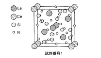
- FIG. 8A is a diagram showing the crystal structure of sample number 1 for the (La, Y) 3 Si 6 N 11 : Ce phosphor.
- FIG. 8B is a diagram showing the crystal structure of sample number 2 for the (La, Y) 3 Si 6 N 11 : Ce phosphor.
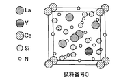
- FIG. 8C is a diagram showing the crystal structure of sample number 3 for the (La, Y) 3 Si 6 N 11 : Ce phosphor.
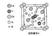
- FIG. 8D is a diagram showing the crystal structure of sample number 4 for the (La, Y) 3 Si 6 N 11 : Ce phosphor.
- FIG. 8E is a diagram showing the crystal structure of sample number 5 for the (La, Y) 3 Si 6 N 11 : Ce phosphor.
- FIG. 8B is a diagram showing the crystal structure of sample number 2 for the (La, Y) 3 Si 6 N 11 : Ce phosphor.
- FIG. 8C is a diagram showing the crystal structure of sample number 3 for the (La, Y) 3 Si
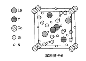
- FIG. 8F is a diagram showing the crystal structure of sample number 6 for the (La, Y) 3 Si 6 N 11 : Ce phosphor.
- FIG. 8G is a diagram showing the crystal structure of sample number 7 for the (La, Y) 3 Si 6 N 11 : Ce phosphor.
- FIG. 8H is a diagram showing the crystal structure of sample number 8 for the (La, Y) 3 Si 6 N 11 : Ce phosphor.
- FIG. 8I is a diagram showing the crystal structure of sample number 9 for the (La, Y) 3 Si 6 N 11 : Ce phosphor.
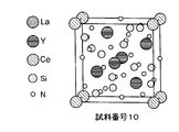
- FIG. 8J is a diagram showing the crystal structure of sample number 10 for the (La, Y) 3 Si 6 N 11 : Ce phosphor.
- FIG. 8G is a diagram showing the crystal structure of sample number 7 for the (La, Y) 3 Si 6 N 11 : Ce phosphor.
- FIG. 8H is a diagram showing the crystal structure of sample number 8 for the (La, Y) 3 Si
- FIG. 9 is a diagram showing powder XRD diffraction pattern results calculated from the crystal structure of the phosphors of sample numbers 1 to 10 shown in FIGS. 8A to 8J.
- FIG. 10 is a schematic cross-sectional view of the LED light emitting device according to the second embodiment.
- FIG. 11 is a schematic cross-sectional view of the LD light-emitting device according to the third embodiment.
- FIG. 12 is a schematic cross-sectional view of the LD light emitting device according to the fourth embodiment.
- FIG. 13 is a schematic cross-sectional view of the lighting apparatus according to the fifth embodiment.
- FIG. 14 is a schematic cross-sectional view of the lighting apparatus according to the sixth embodiment.
- FIG. 15 is a schematic cross-sectional view of a vehicle according to the seventh embodiment.
- the first is a pseudo-white light source that combines a blue LED and a yellow phosphor YAG: Ce.
- This type of light-emitting device is widely used because it can reduce power consumption and easily perform LED drive control.
- this white light source has only two color components, warm light such as a light bulb color cannot be produced, and color control is difficult.
- the second is a white light source that combines a blue LED, a yellow phosphor YAG: Ce, and a red phosphor CASN: Eu.
- white is a mixed color of three color components
- arbitrary white light can be produced by adjusting the light intensity of each color component. Therefore, this type of light-emitting device is easier to control the color than the above-described light-emitting device having two colors of color components.
- the yellow phosphor YAG: Ce used in this light-emitting device has a high quantum efficiency of light emission, and the quantum efficiency of light emission hardly changes even when excited by a high-power blue LED or blue LD.
- the red phosphor CASN Eu has a problem that the quantum efficiency of light emission is lowered when excited with high output light, and is mounted only on a relatively low output light source. This is because a phosphor having an emission center of Eu has a longer emission lifetime than a phosphor having an emission center of Ce, so that the luminance is easily saturated at the time of high output excitation. Therefore, conventionally, it has not been possible to realize a white light source with high output and easy color control.
- the phosphor according to the first aspect of the present disclosure includes a crystal phase having the chemical composition Ce x Y y La 3-xy Si 6 N 11 , and 0 ⁇ x ⁇ 0.6, (1. 5-x) ⁇ y ⁇ (3-x), and has an emission spectrum peak in a wavelength range of 600 nm to 660 nm and a first excitation spectrum peak in a wavelength range of 480 nm to 550 nm.
- a phosphor having Ce as the emission center can be realized.
- the x and the y of the phosphor according to the first aspect may satisfy (1.5 ⁇ 0.5x) ⁇ y ⁇ (3-x).
- the emission wavelength and the excitation wavelength can be increased.
- the x and y of the phosphor according to the second aspect may satisfy 1.5 ⁇ y ⁇ (3-x).
- the phosphor according to the third aspect it is possible to further increase the emission wavelength and the excitation wavelength.
- the crystal phase may have a tetragonal crystal structure.
- the phosphor according to at least one of the first to fourth aspects may have the second peak of the excitation spectrum within a wavelength range of 350 nm or more and less than 480 nm. .
- the phosphor according to the fifth aspect can emit light even with shorter wavelength excitation light such as 450 nm of blue LED and 405 nm of blue-violet LD, the choice of excitation light source is widened.
- the 1 / e emission lifetime of the crystal phase of the phosphor according to at least one of the first to fifth aspects may be 100 ns or less.
- the phosphor according to the sixth aspect is excellent in luminance saturation characteristics, it is promising as a red phosphor having high quantum efficiency even at high output.
- the crystal phase of the phosphor according to at least one of the first to sixth aspects is a La (2a) site in a crystal structure in which Ce is La 3 Si 6 N 11 . It may have a crystal structure that is at least partially substituted.
- the phosphor according to the seventh aspect is suitable for combination with, for example, a green excitation light source because it can emit light even with longer wavelength excitation light.
- the crystal phase of the phosphor according to at least one of the first to seventh aspects is a La (4c) site in a crystal structure in which Y is La 3 Si 6 N 11 . It may have a crystal structure that is at least partially substituted.
- the lattice constants of the a-axis and b-axis of the crystal lattice are The c-axis is relatively extended. For this reason, lattice distortion increases, and as a result, the energy difference between 4f-5d orbits decreases, and the emission wavelength can be lengthened.
- the crystal phase of the phosphor according to the eighth aspect has a crystal structure in which a majority of the La (4c) sites in the crystal structure where Y is La 3 Si 6 N 11 is substituted. You can do it.
- the crystal distortion rapidly increases, and as a result, the wavelength shift toward the long wavelength side increases rapidly, so that red light emission is possible.
- a light emitting device includes an excitation light source that emits light having a wavelength of 600 nm or less, and a first phosphor that is a phosphor according to at least one of the first to ninth aspects. .
- the first phosphor is irradiated with light emitted from the excitation light source and emits fluorescence having a longer wavelength than the light.
- the light-emitting device according to the tenth aspect includes the phosphor according to at least one of the first to ninth aspects, the quantum efficiency can be improved over the conventional light-emitting device at high output. Can do. Furthermore, when the light-emitting device according to the tenth aspect is configured as a white light-emitting device, high color rendering properties and color reproducibility can be realized.
- the excitation light source of the light emitting device according to the tenth aspect may emit light having a wavelength of 480 nm to 600 nm.
- the phosphor can be excited efficiently.
- the excitation light source of the light emitting device according to the tenth aspect may emit light having a wavelength of 420 nm or more and 480 nm or less.
- a GaN blue LED or blue LD can be used as an excitation light source.
- the excitation light source may be an LED or an LD.
- a high-output light emitting device can be realized.
- the light emitting device is irradiated with light emitted from the excitation light source, and emits fluorescence having a longer wavelength than the light.
- the second phosphor may have an emission spectrum peak in a wavelength range of 480 nm or more and less than 600 nm.
- the emission color can be controlled.
- the second phosphor is a phosphor that emits yellow light, is irradiated with light emitted from the excitation light source, and has a longer wavelength than the light.
- a third phosphor that emits the above fluorescence may be further provided, and the third phosphor may emit green light.
- the light emitting device of the fifteenth aspect includes at least two types of phosphors, that is, a phosphor that emits yellow light and a phosphor that emits green light, the emission color can be controlled.
- Embodiment 1 demonstrates embodiment of the fluorescent substance of this indication.
- embodiments of the phosphor of the present disclosure will be described including how the present inventors reached the phosphor of the present disclosure.
- rare earth elements Ce, Pr, Nd, Pm, Sm, Eu, Gd, Tb, Dy, Ho, Er, Tm, and Yb are in the state of divalent or trivalent ions and have valence electrons in the 4f orbit.
- the degeneracy of the 4f orbit is solved and the fragmentation is largely performed as conceptually shown in FIG. 1A.
- light emission can be obtained by utilizing a transition from one 4f level to another 4f level (ff transition). Since the ff transition is a forbidden transition, it has a feature that the lifetime of excited electrons is long. Therefore, a phosphor containing rare earth ions is often used as a laser medium. However, when such a phosphor is used as an incoherent light source such as general illumination, the light emission intensity is saturated immediately.
- Ce 3+ has only one electron in the 4f orbit as a valence electron.
- the split of the 4f orbit of Ce 3+ is extremely small compared to other rare earth ions.
- energy splitting of Eu 2+ and Yb 2+ 4f orbits is small. This is because Eu 2+ is a semi-closed shell with 7 electrons in the 4f orbit and Yb 2+ is a closed shell with 14 electrons in the 4f orbit.
- Ce 3+ , Eu 2+ and Yb 2+ have a small energy difference between the 4f ground level and the 5d orbital because the 4f orbit splitting is small. Further, there is no 4f orbit having a large energy between the 4f ground level and the 5d orbital. Therefore, it is easy to use the transition between 4f and 5d (4f-5d transition).
- the present inventors have further, Ce 3+, focused on Ce 3+ of Eu 2+ and Yb 2+. Since Ce 3+ has one electron involved in the 4f-5d transition, when it falls from the excited state of 5d to the ground state of 4f, all orbits of 4f are vacant, that is, the density of states of the 4f orbit involved in the transition is large. For this reason, the present inventors considered that Ce 3+ has the shortest emission lifetime. On the other hand, Eu 2+ leaves 6 electrons in 4f even when electrons are excited in 5d, and Yb 2+ leaves 13 electrons in 4f even if electrons are excited in 5d.
- Eu 2+ and Yb 2+ have a small density of states of 4f orbits and can be predicted to have a longer emission lifetime than Ce 3+ . Accordingly, it is considered that Ce 3+ phosphor has the shortest emission lifetime among rare earths and is less likely to be saturated with luminance.
- YAG: Ce has a 1 / e emission lifetime of about 70 ns
- CASN Eu has a 1 / e emission lifetime of about 600 to 800 ns.
- the Ce 3+ phosphor is superior to the Eu 2+ phosphor.
- YAG Ce is used for almost all white LEDs on the market.
- CASN Eu is often used as the red phosphor. The present inventors believe that this is because it is difficult to realize a Ce 3+ phosphor that emits red light, and no promising material has yet been found.
- the principle of determining the emission wavelength and the reason will be described.
- ⁇ Emission wavelength of phosphor> In the phosphor having the emission center of Ce 3+ and the phosphor having the emission center of Eu 2+ , the transition from the 4f orbit that is the ground state to the 5d orbit that is the excited state (4f-5d transition) is used.
- Ce 3+ and Eu 2+ are introduced into the crystal that forms the base of the phosphor, the energy of the 4f and 5d orbitals changes mainly under the influence of the closest anion atom (ligand) that is bonded, The emission wavelength changes. That is, the emission wavelength of the phosphor is determined by the host crystal.
- the influence of the ligand is that the energy of the 4f or 5d orbital shifts, and that the degeneration of the five levels of the 5d orbital can be solved (that is, the 5d orbital splitting).
- the former energy shift the way of spreading the wave function of the 4f or 5d orbital and the positional relationship of the ligand greatly influence.
- the latter 5d orbital splitting as shown in FIG. 2, the 5d orbital splits while maintaining the total energy of the five levels of the 5d orbital. Therefore, when the energy of a certain level increases, the energy of other levels decreases. Accordingly, the minimum energy of the 5d orbit can be reduced by increasing the splitting of the 5d orbit.
- the light emission of the 4f-5d transition occurs when it falls from the lowest energy level of the 5d orbit to 4f as shown in FIG. Therefore, by introducing Ce 3+ or Eu 2+ into the crystal, the energy difference between 4f-5d can be reduced and the emission wavelength can be increased.
- Ce 3+ has a large energy difference between 4f-5d in a vacuum (that is, not introduced into the crystal), and emits light in the deep ultraviolet region, while Eu 2+ exhibits blue light emission. That is, Eu 2+ can realize red light emission with a small long wavelength shift amount, and CASN: Eu is actually put into practical use.
- the longest wavelength practically used in Ce 3+ phosphor is YAG: Ce, which is a yellow phosphor, and no red phosphor has been realized.
- the Ce 3+ ligand In order to shift the 5d or 4f orbit, the Ce 3+ ligand must satisfy (1) a small ligand distance and (2) a low symmetry of the ligand. I thought it was important.
- the present inventors calculated the emission wavelength by the method disclosed in the document “Y Jia et al., PHYSICAL REVIEW B 93, 155111 (2016)”. This method calculates the excitation wavelength from the difference between the total energy at the equilibrium point of the ground state and the total energy of the excited state at its atomic coordinates. In this method, the emission wavelength is calculated from the difference between the total energy at the equilibrium point where the excited state is relaxed and the total energy of the ground state at the atomic coordinates.
- YAG Ce
- LaSi 3 N 5 Ce
- La 3 Si 6 N 11 Calculated between excitation and emission wavelengths of the three phosphors of Ce substantially coincides with the experimental value It has been confirmed.
- the (La, Y) 3 Si 6 N 11 : Ce phosphor which is a new composition system, was examined by the above calculation method.
- the phosphor of this composition system has a composition in which the La 3+ site of La 3 Si 6 N 11 : Ce is substituted with Y 3+ . Since the ionic radius of Y 3+ is smaller than that of La 3+ , the ligand distance of Ce 3+ in (La, Y) 3 Si 6 N 11 is smaller than that of La 3 Si 6 N 11 . Thereby, it can be expected that the emission wavelength becomes longer.
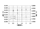
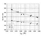
- Table 2 shows the results of calculating the average coordination distance r ave between Ce and N, the excitation wavelength ⁇ ex, and the emission wavelength ⁇ em by changing the substitution amount of Y 3+ .
- FIG. 4 is a graph showing the relationship between the excitation wavelength and the emission wavelength.
- Figure 5 shows the relationship between the lattice constant of the substitution amount x and c-axis of the relationship between the lattice constant of the substitution amount x and the a-axis of Y 3+, and Y 3+.
- FIG. 6 shows the relationship between the average coordination distance r ave and the excitation wavelength ⁇ ex and the relationship between the average coordination distance r ave and the emission wavelength ⁇ em .
- FIG. 7 shows a crystal structure of La 3 Si 6 N 11 and two types of sites of La.
- the La (2a) site is indicated by a broken line
- the La (4c) site is indicated by a one-dot chain line.
- 8A to 8J show the crystal structures of Sample Nos. 1 to 10.
- FIG. 9 shows the powder XRD diffraction pattern results calculated from the crystal structures of sample numbers 1 to 10.
- * mark in Table 2 has shown that the sample is a comparative example.
- the Y substitution site and substitution amount are described as “Y substitution site ⁇ Y substitution amount”.
- the emission wavelength tends to increase as the substitution amount of Y 3+ increases. It can also be seen that the excitation peak wavelength also increases as the emission wavelength increases. It can be seen that in the composition systems of Sample 7 to Sample 10 that emit red light having an emission wavelength of 600 nm or more, the excitation wavelength peak is in the green region of 490 nm or more. Further, as apparent from FIG. 5, it can be seen that the a-axis lattice constant decreases and the c-axis lattice constant increases as the substitution amount of Y 3+ increases. Further, as is apparent from Table 2 and FIG. 6, the average coordination distance r ave between Ce and N decreases as the substitution amount of Y 3+ increases, and both the emission wavelength and the excitation wavelength increase as r ave decreases. I understand that
- the emission lifetime of Eu 2+ is very long compared to the emission lifetime of Ce 3+ .
- the emission lifetime correlates with the transition probability of each 4f-5d transition of Eu 2+ Ce 3+, and it can be said that the longer the emission lifetime, the lower the transition probability.
- the excitation probability of the Eu 2+ 4f-5d transition is very low compared to the excitation probability of the Ce 3+ 4f-5d transition.
- Eu 2+ tends to overlap with the conduction band of the base material ((La, Y) 3 Si 6 N 11 ) in the 5d excitation level. Therefore, energy can be efficiently absorbed between the Eu 2 + 4f ground level and the conduction band of the base material. This absorbed energy corresponds to the energy in the blue light region.
- Eu 2+ has seven electrons in the 4f orbit, and the energy level of each electron has a width, so the excitation wavelength is broad. That is, the excitation wavelength of the red phosphor using Eu 2+ as the emission center is a broad excitation wavelength with the blue region as the peak. Therefore, in the light source using the red phosphor using Eu 2+ as the emission center, blue light having the highest absorption efficiency is used as the excitation light source.
- the 5d excitation level hardly overlaps with the conduction band of the host material. Therefore, energy absorption between the 4f ground level and the base material conduction band cannot be expected. Therefore, the 4f-5d transition is the main energy absorber.
- the present inventors have clarified that in the case of a red phosphor using Ce 3+ , the energy difference between 4f-5d transitions is the energy difference in the green light region. Therefore, in the case of a red phosphor using Ce 3+ , the absorption efficiency of the phosphor is higher when green light is used than when blue light is used as the excitation light source. Therefore, the light output can be increased by using green light. Furthermore, compared with the conventional method of converting blue light to red light, the method of the present application that converts green light to red light can reduce energy conversion loss (Stokes loss), and thus higher output. It becomes possible to emit light.
- Stokes loss energy conversion loss
- ⁇ Phosphor of Embodiment 1 From the above results, the present inventors contain a crystal phase having the chemical composition Ce x Y y La 3-xy Si 6 N 11 as a phosphor according to an embodiment of the present disclosure, and 0 ⁇ x ⁇ A new red phosphor with 0.6 and (1.5 ⁇ x) ⁇ y ⁇ (3-x) was reached.
- the phosphor of Embodiment 1 will be described in more detail.
- x satisfies 0 ⁇ x ⁇ 0.6. Since x is larger than 0, light emission by Ce can be obtained.
- x is preferably 0.0003 or more, more preferably 0.015 or more, from the viewpoint of increasing the emission intensity. There is no particular limitation on the maximum value of x as long as the phosphor can emit light. However, when x becomes too large, the emission intensity decreases due to concentration quenching. Therefore, by setting x to 0.6 or less, it is possible to suppress a decrease in light emission intensity. Further, x is preferably 0.3 or less, more preferably 0.15 or less, from the viewpoint of increasing the emission intensity.
- x and y desirably satisfy (1.5 ⁇ 0.5x) ⁇ y ⁇ (3-x), and 1.5 ⁇ y ⁇ (3- It is more desirable to satisfy x).
- the phosphor of Embodiment 1 has an emission spectrum peak in a wavelength range of 600 nm to 660 nm.
- the phosphor of Embodiment 1 may have an emission spectrum peak with a wavelength of 605 nm or more, for example.
- the phosphor of Embodiment 1 may have, for example, an emission spectrum peak with a wavelength of 640 nm or less, and may have an emission spectrum peak with a wavelength of 636 nm.
- the phosphor of Embodiment 1 has an excitation spectrum peak in a wavelength range of 480 nm to 550 nm.
- the phosphor of Embodiment 1 may have, for example, an excitation spectrum peak with a wavelength of 490 nm or more, or an excitation spectrum peak with a wavelength of 495 nm or more.
- the phosphor of the first embodiment may have, for example, an excitation spectrum peak with a wavelength of 530 nm or less, or an excitation spectrum peak with a wavelength of 508 nm or less.
- the phosphor of the first embodiment has the second excitation spectrum peak within the wavelength range of 350 nm to less than 480 nm when the excitation spectrum peak in the wavelength range of 480 nm to 550 nm is used as the first excitation spectrum peak. May further be included.
- the peak of the first or second excitation spectrum may be the maximum peak of the excitation spectrum.
- the 1 / e emission lifetime of the crystal phase of the phosphor of Embodiment 1 may have a value of 100 ns or less.
- the light emission lifetime affects the luminance saturation characteristic.
- a phosphor containing Eu such as CASN: Eu which is a conventional red phosphor, has a longer emission lifetime than a phosphor containing Ce. Therefore, the phosphor containing Eu is likely to be saturated in luminance due to a decrease in quantum efficiency during high output excitation. Therefore, the phosphor of Embodiment 1 having Ce as the emission center is promising as a red phosphor having a high quantum efficiency even at a high output as compared with the conventional red phosphor.
- the crystal of the base material in the phosphor of Embodiment 1 may be a tetragonal crystal.
- the crystal phase having the chemical composition Ce x Y y La 3-xy Si 6 N 11 in the phosphor of Embodiment 1 may have a tetragonal crystal structure.
- the crystal phase may have almost the same crystal structure as the crystal represented by the general formula La 3 Si 6 N 11 .
- the crystal phase of the phosphor according to Embodiment 1 may have a crystal structure in which Ce substitutes at least a part of the La (2a) site in the crystal structure of La 3 Si 6 N 11 .
- the crystal phase of the phosphor of Embodiment 1 may have a crystal structure in which Y substitutes at least a part of the La (4c) site in the crystal structure of La 3 Si 6 N 11 , where Y is La the majority of La (4c) sites in the crystal structure of 3 Si 6 N 11 may have a crystal structure which is substituted.
- the crystal phase of the phosphor of Embodiment 1 has a crystal structure in which Ce substitutes at least a part of the La (2a) site in the crystal structure of La 3 Si 6 N 11 .
- the crystal phase of the phosphor of Embodiment 1 has a crystal structure in which Y substitutes at least part of the La (4c) site in the crystal structure of La 3 Si 6 N 11 . Further, it is more desirable that Y has a crystal structure in which a majority of La (4c) sites in the crystal structure of La 3 Si 6 N 11 are substituted.
- a compound containing Ce, La, Si and Y may be used, or a single substance of Ce, La, Si and Y may be used.
- a compound that becomes a nitride by firing in a nitrogen atmosphere a high-purity (purity 99% or more) nitride, a metal alloy, or the like can be used.
- a small amount of fluoride such as ammonium fluoride may be added.
- the chemical composition ratio represented by Ce x Y y La 3-xy Si 6 N 11 (0 ⁇ x ⁇ 0.6, (1.5 ⁇ x) ⁇ y ⁇ (3-x))
- a Ce compound, a La compound, a Si compound, and a Y compound may be prepared, where a simple substance of Si may be prepared instead of the Si compound, for example, CeF 3 powder, LaN powder, Si 3 N 4 powder, and YN powder may be used, where CeN powder may be used instead of CeF 3 powder, and Si single powder may be used instead of Si 3 N 4 powder.
- LaN powder may be prepared in excess of about 24% of the theoretical value.LaN is easy to decompose during firing, so by adding excessively at the time of blending raw materials, LaSi, which is a by-product, may be used. Generation of 3 N 5 crystals can be suppressed.
- the phosphor of Embodiment 1 is manufactured by mixing and firing the above raw materials.
- the raw material mixing method may be wet mixing in a solution or dry mixing of a dry powder.
- Firing is performed for about 1 to 50 hours in a temperature range of 1500 to 2000 ° C. in an atmosphere pressurized with nitrogen.
- the pressure at this time is usually 3 atmospheres or more, desirably 4 atmospheres or more, and more desirably 8 atmospheres or more.
- the phosphor after firing may be washed, for example, in a nitric acid solution having a concentration of 10% for 1 hour.
- the obtained phosphor powder may be pulverized again using a ball mill, a jet mill or the like, and further washed or classified as necessary to adjust the particle size distribution or fluidity of the phosphor powder.
- the phosphor according to Embodiment 1 can be used in a light emitting device.
- the light emitting device in the present embodiment includes at least an excitation light source and a first phosphor.
- the excitation light source emits light having a wavelength of 600 nm or less.
- the first phosphor is irradiated with light emitted from the excitation light source and emits fluorescence having a longer wavelength than the light emitted from the excitation light source.
- the first phosphor is, for example, any of the phosphors described in the first embodiment. According to the above configuration, a light emitting device with high quantum efficiency can be configured even at high output.
- the light emitted from the excitation light source may have a wavelength of 480 nm to 600 nm. Since the phosphor of the first embodiment typically has an excitation spectrum peak in the wavelength range of 480 nm to 550 nm, it can be efficiently excited by using an excitation light source that emits light in the above wavelength range. Can do.
- the light emitted from the excitation light source may include light with a wavelength of 200 nm to 480 nm, or may include light with a wavelength of 420 nm to 480 nm.
- the phosphor of Embodiment 1 can absorb excitation light even at a wavelength of 480 nm or less.
- an excitation light source that emits light with a wavelength of 200 nm or more is desirable.
- said excitation light source LED or LD is mentioned, for example.
- the light emitting device in the present embodiment may further include a second phosphor having an emission spectrum peak within a wavelength range of 500 nm to 600 nm. That is, the light emitting device may include a combination of the first phosphor and the second phosphor.
- the second phosphor emits fluorescence having a longer wavelength than the light emitted from the excitation light source when irradiated with the light emitted from the excitation light source.
- a phosphor containing a crystal phase may be used.
- the second phosphor may be a phosphor that emits yellow light, for example.
- the light emitting device may further include a third phosphor that emits green light. That is, the light emitting device may include a combination of a first phosphor, a second phosphor that emits yellow light, and a third phosphor that emits green light.
- the third phosphor emits fluorescence having a longer wavelength than the light emitted from the excitation light source when irradiated with the light emitted from the excitation light source.
- a phosphor containing a crystal phase of the chemical composition Lu 3 Al 5 O 12 : Ce (LuAG: Ce), or a chemical composition Y 3 (Al, Ga) 5 N 12: Ce (YAGG: A phosphor containing a crystal phase having Ce) may be used.
- Green light means light located in the range of (0.1 ⁇ x ⁇ 0.4, 0.5 ⁇ y ⁇ 0.8) in the CIE chromaticity coordinate values.
- Yellow light refers to light positioned in the range of (0.4 ⁇ x ⁇ 0.6, 0.4 ⁇ y ⁇ 0.6) in the CIE chromaticity coordinate values.
- the excitation light source and the second and third phosphors can be freely selected within the above-described range according to the use of the light emitting device. Therefore, the light emitting device including the phosphor according to Embodiment 1 is useful not only as a red light emitting device but also as a white light emitting device. Specifically, a combination of an excitation light source that emits blue light, a phosphor that emits yellow light, and the red phosphor of the present embodiment emits light in a high-color rendering high-output light-emitting device or light bulb color. A high-output light emitting device can be realized.
- Embodiment 2 demonstrates the LED light-emitting device which uses the LED chip as a light emitting element as a light source as an example of the light-emitting device of this indication.
- FIG. 10 is a schematic cross-sectional view showing an embodiment of the LED light-emitting device of Embodiment 2.
- the LED light emitting device 10 includes a phosphor 11, an LED chip 15, and an LED sealing body 24. Further, the LED light emitting device 10 may include a support 23.
- the support body 23 supports the LED chip 15. In this embodiment, since the LED light-emitting device 10 has a structure that can be surface-mounted, the support 23 is a substrate.
- This embodiment can be used for a high-luminance LED light-emitting device.
- the support 23 has a high thermal conductivity so that heat generated in the LED chip 15 can be efficiently radiated to the outside.
- a ceramic substrate made of alumina or aluminum nitride can be used as the support 23.
- the LED chip 15 for example, one that emits light in the ultraviolet to yellow region is used, and one that has an emission spectrum peak within a wavelength range of 200 nm to 600 nm is used. Specifically, a yellow LED chip, a green LED chip, a blue LED chip, a blue-violet LED chip, a near ultraviolet LED chip, an ultraviolet LED chip, or the like is used as the LED chip 15.
- the LED chip 15 is fixed to the support 23 with solder 27 or the like so that the emission surface 15 a does not come into contact with the support 23 on the support 23.
- the LED chip 15 is electrically connected to an electrode 22 provided on the support 23 by a bonding wire 21.
- the LED chip 15 is covered with an LED sealing body 24.
- silicone resin is used for the LED sealing body 24.
- the phosphor 11 is dispersed in the LED sealing body 24.
- the silicone resin a silicone resin having a structure defined by various chemical formulas used as a sealing resin for a semiconductor light emitting device can be used.
- the silicone resin contains, for example, dimethyl silicone having high discoloration resistance.
- methylphenyl silicone etc. with high heat resistance can also be used as a silicone resin.
- the silicone resin may be a homopolymer having a main skeleton with a siloxane bond defined by one chemical formula.
- regulated by 2 or more types of chemical formula, and the alloy of 2 or more types of silicone polymers may be sufficient.
- the silicone resin in the LED sealing body 24 is in a state after being cured. Therefore, the LED sealing body 24 is also in a cured state.
- the LED sealing body 24 can be manufactured using an uncured silicone resin.
- the silicone resin is generally a two-component type in which curing is accelerated by mixing a main agent and a curing agent.
- a thermosetting silicone resin or an energy curable silicone resin that cures when irradiated with energy such as light can also be used.
- FIG. For example, you may use the inorganic material etc. which are comprised from glass, an epoxy resin, ZnO.
- the phosphor 11 may be arranged on the LED sealing body 24 in the form of a phosphor plate without being dispersed in the LED sealing body 24.
- the LED chip is wire bonded, but the LED chip used in the present embodiment may have other configurations. That is, the LED chip used in the present embodiment may be mounted face-up or mounted by flip chip. Moreover, the LED chip used in the present embodiment may include a light emitting layer formed of a nitride semiconductor having a general polar plane (c-plane) growth surface.
- c-plane general polar plane
- the phosphor 11 absorbs a part of wavelength components or all wavelength components in the near ultraviolet to yellow region light (for example, near ultraviolet light) emitted from the LED chip 15 and emits fluorescence.
- the wavelength of light to be absorbed and the wavelength of fluorescence are determined by the type of fluorescent material contained in the phosphor 11.
- the phosphor 11 may be a mixed phosphor including a plurality of phosphors of different colors so that white light is created by the color mixture of light.
- the phosphor 11 may be a mixed phosphor of a green phosphor and a red phosphor. As the red phosphor, the phosphor of the first embodiment is used.
- the phosphor 11 may be a mixed phosphor of a yellow phosphor and a red phosphor.
- the red phosphor the phosphor of the first embodiment is used.
- the yellow phosphor include Y 3 Al 5 O 12 : Ce 3+ , CaSi 2 O 2 N 2 : Eu 2+ , (Ba, Sr) Si 2 O 2 N 2 : Eu 2+ , and Ca 3 Sc 2 Si 3 O.
- Phosphors such as 12 : Ce 3+ , CaSc 2 O 4 : Ce 3+ , ⁇ -SiAlON: Eu 2+ , La 3 Si 6 N 11 : Ce 3+ can be used.
- the particle diameter of the phosphor 11 is, for example, 1 ⁇ m or more and 80 ⁇ m or less, respectively.
- the particle diameter means a circle equivalent diameter measured by a microscopic method.
- the phosphor 11 is included in the LED sealing body 24 at a ratio of 3 parts by weight to 70 parts by weight with respect to 100 parts by weight of the sealing body, for example.
- the weight ratio of the phosphors that emit light of each color used in the phosphor 11 can be appropriately determined according to the desired color tone of white light and the emission intensity of each phosphor.
- the LED light emitting device is configured as an LED light emitting device that emits a color other than white by using only the red phosphor of the first embodiment or combining the phosphor 11 with another color phosphor. You can also.
- the above-described phosphors other than the red phosphor of Embodiment 1 can be manufactured according to a known method. Specifically, in the case of producing an oxide phosphor, as a raw material, a compound that becomes an oxide by firing, such as hydroxide, oxalate, or nitrate, or an oxide can be used. Here, in order to accelerate the reaction, a small amount of fluoride (for example, calcium fluoride) or chloride (for example, calcium chloride) can be added. The phosphor is manufactured by mixing and firing the above raw materials.
- the mixing method of the raw materials may be wet mixing in a solvent or dry mixing of dry powder.
- a ball mill, a medium stirring mill, a planetary mill, a vibration mill, a jet mill, a V-type mixer, a stirrer and the like that are usually used industrially can be used.
- the phosphor material is fired in the air or in a reducing atmosphere at a temperature range of 1100 to 1700 ° C. for about 1 to 50 hours.
- the furnace used for baking can use the furnace normally used industrially.
- a continuous or batch electric furnace such as a pusher furnace or a gas furnace, or a pressure firing furnace such as plasma sintering (SPS) or hot isostatic pressing (HIP) can be used.
- SPS plasma sintering
- HIP hot isostatic pressing
- FIG. 11 shows a schematic configuration of the LD light emitting device 60 according to the third embodiment.
- the LD light emitting device 60 includes an LD element 58 and a wavelength conversion member 61.
- the wavelength conversion member 61 includes a phosphor. The phosphor converts the light emitted from the LD element 58 into light having a longer wavelength.
- the LD element 58 can emit light having a higher optical power density than the LED. Therefore, the use of the LD element 58 can constitute a high-power LD light emitting device 60.
- the optical power density applied to the phosphor from the LD element 58 is, for example, 0.5 W / mm 2 or more. Further, the optical power density is irradiated onto the phosphor may also be 2W / mm 2 or more, may also be 3W / mm 2 or more, may be at 10 W / mm 2 or more.
- the light power density applied to the phosphor may be 150 W / mm 2 or less, 100 W / mm 2 or less, 50 W / mm 2 or less, or 20 W / mm 2. It may be the following.
- an element that emits light having a wavelength capable of exciting the phosphor can be used without particular limitation.
- an LD element that emits blue-violet light, an LD element that emits blue light, an LD element that emits green light, an LD element that emits yellow light, or the like can be used.
- blue light means light having a peak wavelength of 420 nm or more and less than 480 nm.
- the LD element 58 that emits blue light has higher luminous efficiency than the LD element that emits ultraviolet light, and has the highest luminous efficiency when the emission peak wavelength is 445 nm.
- the emission peak wavelength of the LD element 58 may be 425 nm or more, or 430 nm or more. On the other hand, the emission peak wavelength of the LD element 58 may be 475 nm or less, or 470 nm or less.
- the LD element 58 may be composed of one LD, or may be one in which a plurality of LDs are optically coupled.
- the LD element 58 may include a light emitting layer formed of a nitride semiconductor having a growth surface that is a nonpolar surface or a semipolar surface.
- the phosphor of the wavelength conversion member 61 includes the red phosphor of the first embodiment.
- the wavelength conversion member 61 may further include a phosphor other than the red phosphor of the first embodiment according to a desired emission color of the light emitting device.
- the LD light emitting device 60 can be configured as a white light emitting device.
- yellow fluorescent substance and green fluorescent substance what was illustrated in Embodiment 2 can be used.
- the wavelength conversion member 61 may be a single wavelength conversion layer in which a plurality of types of phosphors are mixed, and is a laminate in which at least two wavelength conversion layers including a single type or a plurality of types of phosphors are stacked. May be.
- the wavelength conversion member 61 having a configuration in which a first phosphor layer 62 composed of the red phosphor 12 and a second phosphor layer 63 composed of the yellow phosphor 13 are laminated. The case where is used will be described.
- the first phosphor layer 62 and the second phosphor layer 63 are configured using binders 68 and 69, respectively.
- the binders 68 and 69 are media, such as resin, glass, or a transparent crystal, for example.
- the binders 68 and 69 may be made of the same material or different materials.
- Each phosphor layer may be composed only of phosphor particles.
- An incident optical system 59 that guides the light of the LD element 58 to the second phosphor layer 63 may be provided between the wavelength conversion member 61 and the LD element 58.
- the incident optical system 59 includes, for example, a lens, a mirror, or an optical fiber.
- the blue light emitted from the LD element 58 passes through the incident optical system 59 and enters the second phosphor layer 63 of the wavelength conversion member 61.
- the incident light excites the plurality of yellow phosphors 13 in the second phosphor layer 63 to emit yellow light.
- the blue light emitted from the LD element 58 that has been transmitted without being absorbed by the second phosphor layer 63 is incident on the first phosphor layer 62.
- the plurality of red phosphors 12 in the first phosphor layer 62 are excited and emit red light.
- yellow light emitted from the second phosphor layer 63 is incident on the first phosphor layer 62.
- a part of the incident light may excite the plurality of red phosphors 12 of the first phosphor layer 62 to emit red light. Further, the blue light emitted from the LD element 58 that is transmitted without being absorbed by the first phosphor layer 62 and the second phosphor layer 63 is emitted to the outside. These red light, yellow light, and blue light are mixed to become white light.
- each phosphor layer may be adjusted so that the blue light emitted from the LD element 58 does not pass through the first phosphor layer 62. Further, it may be adjusted so that yellow light emitted from the second phosphor layer 63 does not pass through the first phosphor layer 62. In this case, only red light is emitted to the outside.
- the green phosphor described in the second embodiment may be used in place of the yellow phosphor 13 used in the second phosphor layer 63.
- FIG. 12 shows a schematic configuration of the LD light emitting device 80 according to the fourth embodiment.
- the LD light emitting device 80 includes an LD element 58 and a wavelength conversion member 81.
- the wavelength conversion member 81 includes a phosphor.
- the phosphor converts the light emitted from the LD element 58 into light having a longer wavelength.
- the phosphor of the wavelength conversion member 81 has a wavelength conversion layer in which the red phosphor 12 and at least one selected from the group consisting of the yellow phosphor 13 and the green phosphor 14 are mixed.
- the red phosphor 12 the phosphor of the first embodiment is used.
- yellow fluorescent substance and green fluorescent substance what was illustrated in Embodiment 2 can be used.
- the wavelength conversion member 81 is a phosphor layer formed by mixing three kinds of the red phosphor 12, the yellow phosphor 13, and the green phosphor 14 will be described.
- the mixing ratio of the three types of phosphors can be appropriately adjusted according to the desired color tone of white light, the emission intensity of each phosphor, and the like.
- the phosphor layer that is the wavelength conversion member 81 is configured using a binder 68.
- the binder 68 is a medium such as resin, glass, or transparent crystal.
- the binder 68 may be a single material or may be a different material depending on the location. Note that the phosphor layer may be composed of only phosphor particles.
- the blue light emitted from the LD element 58 passes through the incident optical system 59 and is red, yellow, and green light by the red phosphor 12, the yellow phosphor 13, and the green phosphor 14 in the wavelength conversion member 81, respectively. Is converted to The blue light emitted from the LD element 58 that has not been absorbed by the phosphor is mixed with the red light, yellow light, and green light converted by the red phosphor 12, the yellow phosphor 13, and the green phosphor 14, respectively. White light.
- the red phosphor 12 is excited by part of the green light emitted from the green phosphor 14 and emits red light.
- Embodiment 5 demonstrates an example of the illuminating device of this indication.
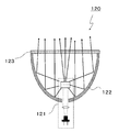
- FIG. 13 shows a schematic configuration of the illumination device 120 according to the fifth embodiment.
- the illumination device 120 includes a light source 121 and an output optical system 122 that guides light emitted from the light source 121 forward.
- a wavelength cut filter 123 that absorbs or reflects light from the light source may be provided.
- the light source 121 includes the red phosphor according to the first embodiment.
- the light source 121 may be the light emitting device 10, 60, or 80 of the second to fourth embodiments.
- the output optical system 122 may be a reflector, for example.
- the emission optical system 122 may include, for example, a metal film such as Al or Ag, or an Al film having a protective film formed on the surface.
- the quantum efficiency can be improved compared to the conventional illumination device at high output. Furthermore, when configured as a white illumination device, high color rendering and color reproducibility can be realized.
- FIG. 14 shows a schematic configuration of the illumination device 130 according to the sixth embodiment.
- the illumination device 130 includes an LD element 58, an incident optical system 59, an optical fiber 132, a wavelength conversion member 131, and an output optical system 122.
- the light emitted from the LD element 58 is guided to the optical fiber 132 through the incident optical system 59.
- the optical fiber 132 guides the light to the emission part.
- the emission unit includes, for example, a wavelength conversion member 131 and an emission optical system 122.
- the wavelength conversion member 131 includes the red phosphor according to the first embodiment. Further, the wavelength conversion member 131 may be the wavelength conversion member 61 or 81 of the third to fourth embodiments.
- the wavelength conversion member 131 may be positioned on the exit side of the optical fiber 132 as shown in FIG. 14, but is on the incident side of the optical fiber 132 (for example, between the LD element 58 and the incident optical system 59, or (Between the incident optical system 59 and the optical fiber 132).
- the light irradiation direction can be easily changed by using an optical fiber.
- the red phosphor of the first embodiment is used, the quantum efficiency can be improved as compared with the conventional illumination device at the time of high output. Furthermore, when configured as a white illumination device, high color rendering and color reproducibility can be realized.
- FIG. 15 shows a schematic configuration of a vehicle 140 according to the seventh embodiment.
- the vehicle 140 includes a vehicle headlamp that is the illumination device 120 of the fifth embodiment, and a power supply source 141.
- the vehicle 140 may include a generator 142 that is rotated by a drive source such as an engine and generates electric power.
- the power generated by the generator 142 may be stored in the power supply source 141.
- the power supply source 141 may be a secondary battery that can be charged and discharged.
- the lighting device 120 is turned on by the power from the power supply source 141.
- the vehicle 140 is, for example, an automobile, a motorcycle, or a special vehicle.
- the vehicle 140 may be an engine vehicle, an electric vehicle, or a hybrid vehicle.
- the vehicle headlamp including the red phosphor of the first embodiment since the vehicle headlamp including the red phosphor of the first embodiment is used, it is possible to illuminate the front more brightly than before when the output is high. Furthermore, when configured as a white illumination device, high color rendering and color reproducibility can be realized.
- the phosphor of the present disclosure is useful as a light emitting device.
- the phosphor of the present disclosure includes, for example, a general lighting device such as a ceiling light, a spotlight, a special lighting device such as a stadium lighting, a studio lighting, a vehicle lighting device such as a headlamp, a projector, a head-up display, etc.
Abstract
Un mode de réalisation de la présente invention concerne une substance fluorescente qui comprend une phase cristalline ayant une composition chimique représentée par CexYyLa3-x-ySi6N11 où 0 0<x≤0,5 et (1,5-x)≤y≤(3-x), et qui donne un spectre d'émission ayant un pic dans la plage de longueurs d'onde de 600 à 660 nm, et donne un spectre d'excitation ayant un premier pic dans la plage de longueurs d'onde de 480 à 600 nm.
Priority Applications (5)
| Application Number | Priority Date | Filing Date | Title |
|---|---|---|---|
| EP17780614.8A EP3480281A4 (fr) | 2016-07-04 | 2017-05-25 | Substance fluorescente et dispositif électroluminescent |
| CN201780001107.XA CN107849448B (zh) | 2016-07-04 | 2017-05-25 | 荧光体以及发光装置 |
| JP2017539670A JP6281801B1 (ja) | 2016-07-04 | 2017-05-25 | 蛍光体および発光装置 |
| KR1020177026995A KR20190028628A (ko) | 2016-07-04 | 2017-05-25 | 형광체 및 발광 장치 |
| US15/723,240 US10955114B2 (en) | 2016-07-04 | 2017-10-03 | Phosphor and light-emitting apparatus |
Applications Claiming Priority (6)
| Application Number | Priority Date | Filing Date | Title |
|---|---|---|---|
| JP2016-132126 | 2016-07-04 | ||
| JP2016132126 | 2016-07-04 | ||
| PCT/JP2017/000935 WO2018008171A1 (fr) | 2016-07-04 | 2017-01-13 | Fluorophore et dispositif électroluminescent |
| JPPCT/JP2017/000935 | 2017-01-13 | ||
| JP2017026910 | 2017-02-16 | ||
| JP2017-026910 | 2017-02-16 |
Related Parent Applications (1)
| Application Number | Title | Priority Date | Filing Date |
|---|---|---|---|
| PCT/JP2017/000935 Continuation WO2018008171A1 (fr) | 2016-07-04 | 2017-01-13 | Fluorophore et dispositif électroluminescent |
Related Child Applications (1)
| Application Number | Title | Priority Date | Filing Date |
|---|---|---|---|
| US15/723,240 Continuation US10955114B2 (en) | 2016-07-04 | 2017-10-03 | Phosphor and light-emitting apparatus |
Publications (1)
| Publication Number | Publication Date |
|---|---|
| WO2018008281A1 true WO2018008281A1 (fr) | 2018-01-11 |
Family
ID=60912504
Family Applications (1)
| Application Number | Title | Priority Date | Filing Date |
|---|---|---|---|
| PCT/JP2017/019464 WO2018008281A1 (fr) | 2016-07-04 | 2017-05-25 | Substance fluorescente et dispositif électroluminescent |
Country Status (6)
| Country | Link |
|---|---|
| US (1) | US10955114B2 (fr) |
| EP (1) | EP3480281A4 (fr) |
| JP (2) | JP6281801B1 (fr) |
| KR (1) | KR20190028628A (fr) |
| CN (1) | CN107849448B (fr) |
| WO (1) | WO2018008281A1 (fr) |
Cited By (1)
| Publication number | Priority date | Publication date | Assignee | Title |
|---|---|---|---|---|
| JPWO2020153260A1 (ja) * | 2019-01-25 | 2021-11-18 | パナソニックIpマネジメント株式会社 | 蛍光体、波長変換部材及び発光装置 |
Families Citing this family (2)
| Publication number | Priority date | Publication date | Assignee | Title |
|---|---|---|---|---|
| CN108895314B (zh) * | 2018-07-06 | 2020-05-15 | 厦门大学 | 激光照明用氮化物荧光粉/玻璃复合光转换组件及其制备 |
| CN115595148B (zh) * | 2022-11-21 | 2023-03-17 | 四川世纪和光科技发展有限公司 | 全色仿生荧光组合物、全色仿生荧光膜和全色仿生光源 |
Citations (5)
| Publication number | Priority date | Publication date | Assignee | Title |
|---|---|---|---|---|
| JP3837588B2 (ja) | 2003-11-26 | 2006-10-25 | 独立行政法人物質・材料研究機構 | 蛍光体と蛍光体を用いた発光器具 |
| JP2008285659A (ja) * | 2007-04-18 | 2008-11-27 | Mitsubishi Chemicals Corp | 蛍光体、蛍光体含有組成物、発光装置、照明装置、画像表示装置、及び窒素含有化合物 |
| JP4459941B2 (ja) | 2006-10-04 | 2010-04-28 | 三菱化学株式会社 | 蛍光体及びその製造方法、並びに、蛍光体含有組成物、発光装置、画像表示装置及び照明装置 |
| JP2014224230A (ja) * | 2013-04-26 | 2014-12-04 | 日亜化学工業株式会社 | 蛍光体及びそれを用いた発光装置並びに蛍光体の製造方法 |
| JP2016028124A (ja) * | 2014-07-08 | 2016-02-25 | 日亜化学工業株式会社 | 蛍光体およびそれを用いた発光装置ならびに蛍光体の製造方法 |
Family Cites Families (59)
| Publication number | Priority date | Publication date | Assignee | Title |
|---|---|---|---|---|
| US4507585A (en) | 1981-09-18 | 1985-03-26 | Hitachi, Ltd. | Beam-indexing color picture tube arrangement |
| US4809291A (en) | 1984-11-26 | 1989-02-28 | Board Of Trustees, Of Leland Stanford Jr U. | Diode pumped laser and doubling to obtain blue light |
| US5246804A (en) | 1988-11-08 | 1993-09-21 | Kyodo Printing Co., Ltd. | Method of retouching pattern |
| US5202891A (en) | 1991-12-23 | 1993-04-13 | State Of Oregon Acting By And Through The State Board Of Higher Education On Behalf Of Oregon State University | Nonlinear optical material |
| DE69529700T2 (de) | 1994-06-03 | 2003-10-16 | Agfa Gevaert Nv | Neue Klasse von hochenergetischen Detektionsmaterialien |
| US6569156B1 (en) | 2000-06-30 | 2003-05-27 | Nikolai Tankovich | Medical cosmetic laser with second wavelength enhancement |
| US7554258B2 (en) | 2002-10-22 | 2009-06-30 | Osram Opto Semiconductors Gmbh | Light source having an LED and a luminescence conversion body and method for producing the luminescence conversion body |
| US7094362B2 (en) | 2003-10-29 | 2006-08-22 | General Electric Company | Garnet phosphor materials having enhanced spectral characteristics |
| TWI263356B (en) | 2003-11-27 | 2006-10-01 | Kuen-Juei Li | Light-emitting device |
| DE10360546A1 (de) | 2003-12-22 | 2005-07-14 | Patent-Treuhand-Gesellschaft für elektrische Glühlampen mbH | Leuchtstoff und Lichtquelle mit derartigem Leuchtstoff |
| EP1727249B1 (fr) | 2004-03-10 | 2014-02-12 | Panasonic Corporation | Source de lumière cohérente et système optique |
| US20080262316A1 (en) | 2004-07-28 | 2008-10-23 | Kyocera Corporation | Light Source Apparatus and Endoscope Provided with Light Source Apparatus |
| JP5081370B2 (ja) | 2004-08-31 | 2012-11-28 | 日亜化学工業株式会社 | 発光装置 |
| JP4679183B2 (ja) | 2005-03-07 | 2011-04-27 | シチズン電子株式会社 | 発光装置及び照明装置 |
| JP5046223B2 (ja) | 2005-05-24 | 2012-10-10 | 独立行政法人物質・材料研究機構 | 蛍光体及びその利用 |
| WO2006126567A1 (fr) | 2005-05-24 | 2006-11-30 | Mitsubishi Chemical Corporation | Luminophore et son utilisation |
| JP2009510230A (ja) | 2005-09-30 | 2009-03-12 | ザ リージェンツ オブ ザ ユニバーシティ オブ カリフォルニア | 固体照明用途のニトリドおよびオキシニトリドセリウム系蛍光体材料 |
| KR101200400B1 (ko) | 2005-12-01 | 2012-11-16 | 삼성전자주식회사 | 백색 발광 다이오드 |
| JP4228012B2 (ja) | 2006-12-20 | 2009-02-25 | Necライティング株式会社 | 赤色発光窒化物蛍光体およびそれを用いた白色発光素子 |
| JP2008177484A (ja) | 2007-01-22 | 2008-07-31 | Central Glass Co Ltd | 可視光発光材料および可視光発光装置 |
| JP2009153712A (ja) | 2007-12-26 | 2009-07-16 | Olympus Corp | 光源装置およびそれを備えた内視鏡装置 |
| TWI438262B (zh) | 2008-02-07 | 2014-05-21 | Mitsubishi Chem Corp | A semiconductor light emitting device, a backlight, a color image display device, and a phosphor |
| JP5350643B2 (ja) | 2008-02-13 | 2013-11-27 | 富士フイルム株式会社 | 内視鏡装置 |
| JP4466758B2 (ja) | 2008-04-03 | 2010-05-26 | 三菱化学株式会社 | 蛍光体及びその製造方法、蛍光体含有組成物、発光装置、照明装置並びに画像表示装置 |
| EP2130484B1 (fr) | 2008-06-04 | 2011-04-20 | FUJIFILM Corporation | Dispositif d'éclairage à utiliser dans un endoscope |
| JP5216429B2 (ja) | 2008-06-13 | 2013-06-19 | 富士フイルム株式会社 | 光源装置および内視鏡装置 |
| CN102124263B (zh) | 2008-06-25 | 2013-07-24 | 克里公司 | 包括光混合的固态照明装置 |
| JP2010114040A (ja) | 2008-11-10 | 2010-05-20 | Toyota Motor Corp | 燃料電池システムの運転方法 |
| CN102361956B (zh) | 2009-03-31 | 2014-10-29 | 三菱化学株式会社 | 荧光体、荧光体的制造方法、含荧光体组合物、发光装置、照明装置和图像显示装置 |
| JP5767775B2 (ja) | 2009-07-06 | 2015-08-19 | 富士フイルム株式会社 | 内視鏡装置 |
| WO2012017949A1 (fr) * | 2010-08-04 | 2012-02-09 | 宇部興産株式会社 | POUDRE DE NITRURE DE SILICIUM POUR LUMINOPHORE AU NITRURE DE SILICIUM, LUMINOPHORE EN CaAlSiN3 L'UTILISANT, LUMINOPHORE EN Sr2Si5N8 L'UTILISANT, LUMINOPHORE EN (Sr, Ca)AlSiN3 L'UTILISANT, LUMINOPHORE EN La3Si6N11 L'UTILISANT ET PROCÉDÉS POUR LA PRODUCTION DES LUMINOPHORES |
| TWI424047B (zh) | 2011-01-24 | 2014-01-21 | Univ Nat Chiao Tung | 紅光和綠光之氟硫化物螢光材料、製備方法與其白光發光二極體裝置 |
| JP5842162B2 (ja) | 2011-03-23 | 2016-01-13 | パナソニックIpマネジメント株式会社 | 光源装置及びそれを用いた画像表示装置 |
| JP5331904B2 (ja) | 2011-04-15 | 2013-10-30 | 富士フイルム株式会社 | 内視鏡システム及び内視鏡システムの作動方法 |
| US8513900B2 (en) | 2011-05-12 | 2013-08-20 | Ledengin, Inc. | Apparatus for tuning of emitter with multiple LEDs to a single color bin |
| JP5611892B2 (ja) | 2011-05-24 | 2014-10-22 | 富士フイルム株式会社 | 内視鏡システム及び内視鏡システムの作動方法 |
| JP5870259B2 (ja) | 2011-05-25 | 2016-02-24 | パナソニックIpマネジメント株式会社 | 照明装置および該照明装置を備える投射型表示装置 |
| KR101873221B1 (ko) * | 2011-12-09 | 2018-07-06 | 삼성전자주식회사 | 형광체 및 발광장치 |
| CN102543986A (zh) | 2012-01-04 | 2012-07-04 | 歌尔声学股份有限公司 | 发光二极管装置 |
| KR101957701B1 (ko) | 2012-11-14 | 2019-03-14 | 삼성전자주식회사 | 발광소자 패키지 및 그 제조방법 |
| US9335027B2 (en) | 2013-01-02 | 2016-05-10 | Massachusetts Institute Of Technology | Methods and apparatus for transparent display using scattering nanoparticles |
| JP5928383B2 (ja) * | 2013-03-22 | 2016-06-01 | ソニー株式会社 | 光源装置および表示装置 |
| CN103148395B (zh) * | 2013-03-27 | 2015-06-17 | 中国科学院重庆绿色智能技术研究院 | 基于激光器、光纤和发光部的白光光源及发光部制备方法 |
| WO2015025570A1 (fr) | 2013-08-20 | 2015-02-26 | 電気化学工業株式会社 | Substance électroluminescente, dispositif électroluminescent et procédé de production d'une substance électroluminescente |
| CN105706256B (zh) | 2013-11-08 | 2018-03-13 | 夏普株式会社 | 发光装置以及照明装置 |
| US9725648B2 (en) * | 2013-12-10 | 2017-08-08 | Samsung Electronics Co., Ltd. | Phosphor and light-emitting device including the same |
| CN103715342B (zh) | 2013-12-30 | 2016-04-06 | 姜虹 | Led光源的制备方法及含有该光源的led灯 |
| US10104726B2 (en) | 2014-01-28 | 2018-10-16 | Sharp Kabushiki Kaisha | Light emitting diode drive device and illumination device |
| RU2648080C1 (ru) | 2014-09-11 | 2018-03-22 | Филипс Лайтинг Холдинг Б.В. | Сид-модуль с преобразованием люминофором с улучшенными передачей белого цвета и эффективностью преобразования |
| CN107109220B (zh) | 2014-10-31 | 2020-04-10 | 亮锐控股有限公司 | 具有温度稳定通量和饱和红色色点的磷光体转换led |
| JP6428193B2 (ja) | 2014-11-21 | 2018-11-28 | 日亜化学工業株式会社 | 波長変換部材および該波長変換部材を備えたプロジェクタ |
| JPWO2016092743A1 (ja) | 2014-12-12 | 2017-11-24 | パナソニックIpマネジメント株式会社 | 発光装置 |
| DE102015106757A1 (de) | 2015-04-30 | 2016-11-03 | Osram Opto Semiconductors Gmbh | Strahlungsemittierendes optoelektronisches Bauelement |
| US10026876B2 (en) * | 2015-08-20 | 2018-07-17 | Nichia Corporation | Light emitting device |
| JP6215981B2 (ja) | 2016-02-18 | 2017-10-18 | オリンパス株式会社 | 光源装置およびそれを備えた内視鏡装置 |
| CN107305921A (zh) | 2016-04-20 | 2017-10-31 | 松下知识产权经营株式会社 | 波长转换部件、光源以及车辆用前照灯 |
| KR20190065192A (ko) | 2016-10-21 | 2019-06-11 | 니폰 덴키 가라스 가부시키가이샤 | 파장 변환 부재, 발광 디바이스 및 파장 변환 부재의 제조 방법 |
| JP7042457B2 (ja) | 2017-06-06 | 2022-03-28 | パナソニックIpマネジメント株式会社 | 蛍光体および発光装置 |
| JP7108841B2 (ja) | 2017-12-08 | 2022-07-29 | パナソニックIpマネジメント株式会社 | 蛍光体および発光装置 |
-
2017
- 2017-05-25 EP EP17780614.8A patent/EP3480281A4/fr not_active Withdrawn
- 2017-05-25 JP JP2017539670A patent/JP6281801B1/ja active Active
- 2017-05-25 CN CN201780001107.XA patent/CN107849448B/zh active Active
- 2017-05-25 WO PCT/JP2017/019464 patent/WO2018008281A1/fr unknown
- 2017-05-25 KR KR1020177026995A patent/KR20190028628A/ko unknown
- 2017-10-03 US US15/723,240 patent/US10955114B2/en active Active
-
2018
- 2018-01-11 JP JP2018002590A patent/JP2018131605A/ja active Pending
Patent Citations (6)
| Publication number | Priority date | Publication date | Assignee | Title |
|---|---|---|---|---|
| JP3837588B2 (ja) | 2003-11-26 | 2006-10-25 | 独立行政法人物質・材料研究機構 | 蛍光体と蛍光体を用いた発光器具 |
| JP4459941B2 (ja) | 2006-10-04 | 2010-04-28 | 三菱化学株式会社 | 蛍光体及びその製造方法、並びに、蛍光体含有組成物、発光装置、画像表示装置及び照明装置 |
| JP2008285659A (ja) * | 2007-04-18 | 2008-11-27 | Mitsubishi Chemicals Corp | 蛍光体、蛍光体含有組成物、発光装置、照明装置、画像表示装置、及び窒素含有化合物 |
| JP2010084151A (ja) * | 2007-04-18 | 2010-04-15 | Mitsubishi Chemicals Corp | 蛍光体 |
| JP2014224230A (ja) * | 2013-04-26 | 2014-12-04 | 日亜化学工業株式会社 | 蛍光体及びそれを用いた発光装置並びに蛍光体の製造方法 |
| JP2016028124A (ja) * | 2014-07-08 | 2016-02-25 | 日亜化学工業株式会社 | 蛍光体およびそれを用いた発光装置ならびに蛍光体の製造方法 |
Non-Patent Citations (2)
| Title |
|---|
| See also references of EP3480281A4 |
| Y JIA ET AL., PHYSICAL REVIEW B, vol. 93, 2016, pages 155111 |
Cited By (2)
| Publication number | Priority date | Publication date | Assignee | Title |
|---|---|---|---|---|
| JPWO2020153260A1 (ja) * | 2019-01-25 | 2021-11-18 | パナソニックIpマネジメント株式会社 | 蛍光体、波長変換部材及び発光装置 |
| JP7142303B2 (ja) | 2019-01-25 | 2022-09-27 | パナソニックIpマネジメント株式会社 | 蛍光体、波長変換部材及び発光装置 |
Also Published As
| Publication number | Publication date |
|---|---|
| KR20190028628A (ko) | 2019-03-19 |
| US10955114B2 (en) | 2021-03-23 |
| EP3480281A1 (fr) | 2019-05-08 |
| EP3480281A4 (fr) | 2019-07-31 |
| CN107849448A (zh) | 2018-03-27 |
| US20180038575A1 (en) | 2018-02-08 |
| JPWO2018008281A1 (ja) | 2018-07-12 |
| CN107849448B (zh) | 2022-04-15 |
| JP6281801B1 (ja) | 2018-02-21 |
| JP2018131605A (ja) | 2018-08-23 |
Similar Documents
| Publication | Publication Date | Title |
|---|---|---|
| EP3480863B1 (fr) | Dispositif électroluminescent utilisant du fluorophore | |
| JP7042457B2 (ja) | 蛍光体および発光装置 | |
| JP6206696B1 (ja) | 蛍光体および発光装置 | |
| CN108138045B (zh) | 荧光体以及发光装置 | |
| EP3495448B1 (fr) | Phosphore et appareil électroluminescent | |
| KR20140043055A (ko) | 카보니트라이드 및 카바이도니트라이드 형광체 및 이를 사용한 발광 장치 | |
| JP6281801B1 (ja) | 蛍光体および発光装置 | |
| JP2015061902A (ja) | 黄色蛍光体、発光デバイス、照明装置、および車両 | |
| JP7022931B2 (ja) | 蛍光体および発光装置 | |
| CN112608739A (zh) | 红色荧光体以及使用其的发光装置 |
Legal Events
| Date | Code | Title | Description |
|---|---|---|---|
| ENP | Entry into the national phase |
Ref document number: 2017539670 Country of ref document: JP Kind code of ref document: A |
|
| ENP | Entry into the national phase |
Ref document number: 20177026995 Country of ref document: KR Kind code of ref document: A |
|
| 121 | Ep: the epo has been informed by wipo that ep was designated in this application |
Ref document number: 17780614 Country of ref document: EP Kind code of ref document: A1 |
|
| NENP | Non-entry into the national phase |
Ref country code: DE |