WO2018008171A1 - 蛍光体および発光装置 - Google Patents
蛍光体および発光装置 Download PDFInfo
- Publication number
- WO2018008171A1 WO2018008171A1 PCT/JP2017/000935 JP2017000935W WO2018008171A1 WO 2018008171 A1 WO2018008171 A1 WO 2018008171A1 JP 2017000935 W JP2017000935 W JP 2017000935W WO 2018008171 A1 WO2018008171 A1 WO 2018008171A1
- Authority
- WO
- WIPO (PCT)
- Prior art keywords
- phosphor
- light
- wavelength
- emission
- peak
- Prior art date
Links
Images


Classifications
-
- C—CHEMISTRY; METALLURGY
- C09—DYES; PAINTS; POLISHES; NATURAL RESINS; ADHESIVES; COMPOSITIONS NOT OTHERWISE PROVIDED FOR; APPLICATIONS OF MATERIALS NOT OTHERWISE PROVIDED FOR
- C09K—MATERIALS FOR MISCELLANEOUS APPLICATIONS, NOT PROVIDED FOR ELSEWHERE
- C09K11/00—Luminescent, e.g. electroluminescent, chemiluminescent materials
- C09K11/08—Luminescent, e.g. electroluminescent, chemiluminescent materials containing inorganic luminescent materials
- C09K11/77—Luminescent, e.g. electroluminescent, chemiluminescent materials containing inorganic luminescent materials containing rare earth metals
- C09K11/7766—Luminescent, e.g. electroluminescent, chemiluminescent materials containing inorganic luminescent materials containing rare earth metals containing two or more rare earth metals
- C09K11/77747—Silicon Nitrides or Silicon Oxynitrides
-
- C—CHEMISTRY; METALLURGY
- C09—DYES; PAINTS; POLISHES; NATURAL RESINS; ADHESIVES; COMPOSITIONS NOT OTHERWISE PROVIDED FOR; APPLICATIONS OF MATERIALS NOT OTHERWISE PROVIDED FOR
- C09K—MATERIALS FOR MISCELLANEOUS APPLICATIONS, NOT PROVIDED FOR ELSEWHERE
- C09K11/00—Luminescent, e.g. electroluminescent, chemiluminescent materials
- C09K11/08—Luminescent, e.g. electroluminescent, chemiluminescent materials containing inorganic luminescent materials
- C09K11/77—Luminescent, e.g. electroluminescent, chemiluminescent materials containing inorganic luminescent materials containing rare earth metals
- C09K11/7715—Luminescent, e.g. electroluminescent, chemiluminescent materials containing inorganic luminescent materials containing rare earth metals containing cerium
- C09K11/77217—Silicon Nitrides or Silicon Oxynitrides
-
- C—CHEMISTRY; METALLURGY
- C09—DYES; PAINTS; POLISHES; NATURAL RESINS; ADHESIVES; COMPOSITIONS NOT OTHERWISE PROVIDED FOR; APPLICATIONS OF MATERIALS NOT OTHERWISE PROVIDED FOR
- C09K—MATERIALS FOR MISCELLANEOUS APPLICATIONS, NOT PROVIDED FOR ELSEWHERE
- C09K11/00—Luminescent, e.g. electroluminescent, chemiluminescent materials
- C09K11/08—Luminescent, e.g. electroluminescent, chemiluminescent materials containing inorganic luminescent materials
- C09K11/77—Luminescent, e.g. electroluminescent, chemiluminescent materials containing inorganic luminescent materials containing rare earth metals
- C09K11/7715—Luminescent, e.g. electroluminescent, chemiluminescent materials containing inorganic luminescent materials containing rare earth metals containing cerium
- C09K11/77218—Silicon Aluminium Nitrides or Silicon Aluminium Oxynitrides
-
- C—CHEMISTRY; METALLURGY
- C09—DYES; PAINTS; POLISHES; NATURAL RESINS; ADHESIVES; COMPOSITIONS NOT OTHERWISE PROVIDED FOR; APPLICATIONS OF MATERIALS NOT OTHERWISE PROVIDED FOR
- C09K—MATERIALS FOR MISCELLANEOUS APPLICATIONS, NOT PROVIDED FOR ELSEWHERE
- C09K11/00—Luminescent, e.g. electroluminescent, chemiluminescent materials
- C09K11/08—Luminescent, e.g. electroluminescent, chemiluminescent materials containing inorganic luminescent materials
- C09K11/77—Luminescent, e.g. electroluminescent, chemiluminescent materials containing inorganic luminescent materials containing rare earth metals
- C09K11/7728—Luminescent, e.g. electroluminescent, chemiluminescent materials containing inorganic luminescent materials containing rare earth metals containing europium
- C09K11/7734—Aluminates
-
- C—CHEMISTRY; METALLURGY
- C09—DYES; PAINTS; POLISHES; NATURAL RESINS; ADHESIVES; COMPOSITIONS NOT OTHERWISE PROVIDED FOR; APPLICATIONS OF MATERIALS NOT OTHERWISE PROVIDED FOR
- C09K—MATERIALS FOR MISCELLANEOUS APPLICATIONS, NOT PROVIDED FOR ELSEWHERE
- C09K11/00—Luminescent, e.g. electroluminescent, chemiluminescent materials
- C09K11/08—Luminescent, e.g. electroluminescent, chemiluminescent materials containing inorganic luminescent materials
- C09K11/77—Luminescent, e.g. electroluminescent, chemiluminescent materials containing inorganic luminescent materials containing rare earth metals
- C09K11/7766—Luminescent, e.g. electroluminescent, chemiluminescent materials containing inorganic luminescent materials containing rare earth metals containing two or more rare earth metals
- C09K11/7774—Aluminates
-
- C—CHEMISTRY; METALLURGY
- C09—DYES; PAINTS; POLISHES; NATURAL RESINS; ADHESIVES; COMPOSITIONS NOT OTHERWISE PROVIDED FOR; APPLICATIONS OF MATERIALS NOT OTHERWISE PROVIDED FOR
- C09K—MATERIALS FOR MISCELLANEOUS APPLICATIONS, NOT PROVIDED FOR ELSEWHERE
- C09K11/00—Luminescent, e.g. electroluminescent, chemiluminescent materials
- C09K11/08—Luminescent, e.g. electroluminescent, chemiluminescent materials containing inorganic luminescent materials
- C09K11/77—Luminescent, e.g. electroluminescent, chemiluminescent materials containing inorganic luminescent materials containing rare earth metals
- C09K11/7766—Luminescent, e.g. electroluminescent, chemiluminescent materials containing inorganic luminescent materials containing rare earth metals containing two or more rare earth metals
- C09K11/77748—Silicon Aluminium Nitrides or Silicon Aluminium Oxynitrides
-
- F—MECHANICAL ENGINEERING; LIGHTING; HEATING; WEAPONS; BLASTING
- F21—LIGHTING
- F21S—NON-PORTABLE LIGHTING DEVICES; SYSTEMS THEREOF; VEHICLE LIGHTING DEVICES SPECIALLY ADAPTED FOR VEHICLE EXTERIORS
- F21S41/00—Illuminating devices specially adapted for vehicle exteriors, e.g. headlamps
- F21S41/10—Illuminating devices specially adapted for vehicle exteriors, e.g. headlamps characterised by the light source
- F21S41/14—Illuminating devices specially adapted for vehicle exteriors, e.g. headlamps characterised by the light source characterised by the type of light source
- F21S41/176—Light sources where the light is generated by photoluminescent material spaced from a primary light generating element
-
- H—ELECTRICITY
- H01—ELECTRIC ELEMENTS
- H01L—SEMICONDUCTOR DEVICES NOT COVERED BY CLASS H10
- H01L33/00—Semiconductor devices with at least one potential-jump barrier or surface barrier specially adapted for light emission; Processes or apparatus specially adapted for the manufacture or treatment thereof or of parts thereof; Details thereof
- H01L33/48—Semiconductor devices with at least one potential-jump barrier or surface barrier specially adapted for light emission; Processes or apparatus specially adapted for the manufacture or treatment thereof or of parts thereof; Details thereof characterised by the semiconductor body packages
- H01L33/50—Wavelength conversion elements
- H01L33/501—Wavelength conversion elements characterised by the materials, e.g. binder
- H01L33/502—Wavelength conversion materials
- H01L33/504—Elements with two or more wavelength conversion materials
-
- H—ELECTRICITY
- H01—ELECTRIC ELEMENTS
- H01S—DEVICES USING THE PROCESS OF LIGHT AMPLIFICATION BY STIMULATED EMISSION OF RADIATION [LASER] TO AMPLIFY OR GENERATE LIGHT; DEVICES USING STIMULATED EMISSION OF ELECTROMAGNETIC RADIATION IN WAVE RANGES OTHER THAN OPTICAL
- H01S5/00—Semiconductor lasers
- H01S5/005—Optical components external to the laser cavity, specially adapted therefor, e.g. for homogenisation or merging of the beams or for manipulating laser pulses, e.g. pulse shaping
- H01S5/0087—Optical components external to the laser cavity, specially adapted therefor, e.g. for homogenisation or merging of the beams or for manipulating laser pulses, e.g. pulse shaping for illuminating phosphorescent or fluorescent materials, e.g. using optical arrangements specifically adapted for guiding or shaping laser beams illuminating these materials
-
- H—ELECTRICITY
- H01—ELECTRIC ELEMENTS
- H01S—DEVICES USING THE PROCESS OF LIGHT AMPLIFICATION BY STIMULATED EMISSION OF RADIATION [LASER] TO AMPLIFY OR GENERATE LIGHT; DEVICES USING STIMULATED EMISSION OF ELECTROMAGNETIC RADIATION IN WAVE RANGES OTHER THAN OPTICAL
- H01S5/00—Semiconductor lasers
- H01S5/02—Structural details or components not essential to laser action
- H01S5/022—Mountings; Housings
- H01S5/02208—Mountings; Housings characterised by the shape of the housings
- H01S5/02212—Can-type, e.g. TO-CAN housings with emission along or parallel to symmetry axis
-
- H—ELECTRICITY
- H01—ELECTRIC ELEMENTS
- H01S—DEVICES USING THE PROCESS OF LIGHT AMPLIFICATION BY STIMULATED EMISSION OF RADIATION [LASER] TO AMPLIFY OR GENERATE LIGHT; DEVICES USING STIMULATED EMISSION OF ELECTROMAGNETIC RADIATION IN WAVE RANGES OTHER THAN OPTICAL
- H01S5/00—Semiconductor lasers
- H01S5/30—Structure or shape of the active region; Materials used for the active region
- H01S5/32—Structure or shape of the active region; Materials used for the active region comprising PN junctions, e.g. hetero- or double- heterostructures
- H01S5/323—Structure or shape of the active region; Materials used for the active region comprising PN junctions, e.g. hetero- or double- heterostructures in AIIIBV compounds, e.g. AlGaAs-laser, InP-based laser
- H01S5/32308—Structure or shape of the active region; Materials used for the active region comprising PN junctions, e.g. hetero- or double- heterostructures in AIIIBV compounds, e.g. AlGaAs-laser, InP-based laser emitting light at a wavelength less than 900 nm
- H01S5/32341—Structure or shape of the active region; Materials used for the active region comprising PN junctions, e.g. hetero- or double- heterostructures in AIIIBV compounds, e.g. AlGaAs-laser, InP-based laser emitting light at a wavelength less than 900 nm blue laser based on GaN or GaP
-
- H—ELECTRICITY
- H05—ELECTRIC TECHNIQUES NOT OTHERWISE PROVIDED FOR
- H05B—ELECTRIC HEATING; ELECTRIC LIGHT SOURCES NOT OTHERWISE PROVIDED FOR; CIRCUIT ARRANGEMENTS FOR ELECTRIC LIGHT SOURCES, IN GENERAL
- H05B33/00—Electroluminescent light sources
- H05B33/12—Light sources with substantially two-dimensional radiating surfaces
- H05B33/14—Light sources with substantially two-dimensional radiating surfaces characterised by the chemical or physical composition or the arrangement of the electroluminescent material, or by the simultaneous addition of the electroluminescent material in or onto the light source
-
- C—CHEMISTRY; METALLURGY
- C01—INORGANIC CHEMISTRY
- C01P—INDEXING SCHEME RELATING TO STRUCTURAL AND PHYSICAL ASPECTS OF SOLID INORGANIC COMPOUNDS
- C01P2002/00—Crystal-structural characteristics
- C01P2002/70—Crystal-structural characteristics defined by measured X-ray, neutron or electron diffraction data
-
- Y—GENERAL TAGGING OF NEW TECHNOLOGICAL DEVELOPMENTS; GENERAL TAGGING OF CROSS-SECTIONAL TECHNOLOGIES SPANNING OVER SEVERAL SECTIONS OF THE IPC; TECHNICAL SUBJECTS COVERED BY FORMER USPC CROSS-REFERENCE ART COLLECTIONS [XRACs] AND DIGESTS
- Y02—TECHNOLOGIES OR APPLICATIONS FOR MITIGATION OR ADAPTATION AGAINST CLIMATE CHANGE
- Y02B—CLIMATE CHANGE MITIGATION TECHNOLOGIES RELATED TO BUILDINGS, e.g. HOUSING, HOUSE APPLIANCES OR RELATED END-USER APPLICATIONS
- Y02B20/00—Energy efficient lighting technologies, e.g. halogen lamps or gas discharge lamps
Definitions
- the present disclosure relates to a phosphor and a light emitting device.
- the current general white LED has a configuration in which a blue light emitting element (blue LED chip) and a phosphor are combined.
- a blue light emitting element blue LED chip
- a phosphor a part of the light from the blue LED chip is color-converted by the phosphor, and the blue light from the blue LED chip and the light emitted from the phosphor are mixed to produce white light.
- LD Laser Diode
- a blue LED chip or a combination of blue LD and yellow phosphor is mainly used as a white solid light source.
- a blue light source is used for the purpose of improving color rendering, color reproducibility, etc., or obtaining white having a low color temperature.
- a white light source that combines a red phosphor with a yellow phosphor has been developed.
- Patent Document 1 the general formula Y 3 Al 5 O 12 : Ce 3+ (hereinafter abbreviated as YAG: Ce) and the general formula La 3 Si 6 N 11 : Ce 3+ (hereinafter abbreviated as LSN: Ce) shown in Patent Document 1.
- yellow phosphors having Ce as the emission center are known.
- a red phosphor having Eu as the emission center is known, as in the general formula (Sr, Ca) AlSiN 3 : Eu 2+ (hereinafter abbreviated as CASN: Eu) shown in Patent Document 2.
- the present disclosure provides a phosphor having an emission center of Ce.
- the phosphor in one embodiment of the present disclosure contains a crystalline phase having the chemical composition Ce x M 3-xy ⁇ 6 ⁇ 11-z .
- M is one or more elements selected from the group consisting of Sc, Y, La, Pr, Nd, Sm, Eu, Gd, Tb, Dy, Ho, Er, Tm, Yb, and Lu.
- ⁇ contains 50 mol% or more of Si.
- ⁇ contains 80 mol% or more of N. 0 ⁇ x ⁇ 0.6. 0 ⁇ y ⁇ 1.0. 0 ⁇ z ⁇ 1.0. It has a maximum peak of the emission spectrum at a wavelength of 600 nm to 800 nm.
- the first peak of the excitation spectrum is present at a wavelength of 500 nm to 600 nm.
- the comprehensive or specific aspect of the present disclosure may be realized by a phosphor, an element, an apparatus, a system, a vehicle, a manufacturing method, or any combination thereof.
- the phosphor of the present disclosure has Ce as the emission center.
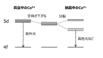
- FIG. 1 is an energy level diagram of Ce 3+ in vacuum and in a crystal.
- FIG. 2 is a coordination coordinate model diagram between the 4f trajectory and the 5d trajectory.
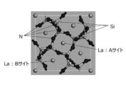
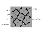
- FIG. 3 is a diagram showing a 1 ⁇ 1 ⁇ 3 supercell structure of La 3 Si 6 N 11 after structure optimization.
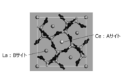
- FIG. 4 is a diagram showing a 1 ⁇ 1 ⁇ 3 supercell structure of La 3 Si 6 N 11 : Ce after La is replaced with Ce and structural optimization is performed.
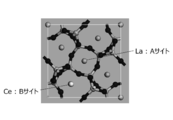
- FIG. 5 is a diagram showing a 1 ⁇ 1 ⁇ 3 supercell structure of La 3 Si 6 N 11 : Ce after La is replaced with Ce and structure optimization is performed.
- FIG. 1 is an energy level diagram of Ce 3+ in vacuum and in a crystal.
- FIG. 2 is a coordination coordinate model diagram between the 4f trajectory and the 5d trajectory.
- FIG. 3 is a diagram showing a 1 ⁇ 1 ⁇ 3 supercell structure of La 3 Si 6 N 11 after structure optimization.
- FIG. 4 is a diagram showing a
- FIG. 6 shows La 3 Si 6 N 11 : Ce 1 ⁇ 1 ⁇ 3 after structural optimization by replacing La at the A site with Ce, replacing the Si site with Al, and replacing the N site with O. It is a figure which shows a supercell structure.
- FIG. 7 shows La 3 Si 6 N 11 : Ce 1 ⁇ 1 ⁇ 3 after structural optimization by substituting Ce for La at B site, Al for Si site and O for N site. It is a figure which shows a supercell structure.
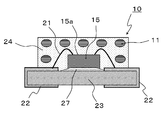
- FIG. 8 is a schematic cross-sectional view of the LED light-emitting device according to the second embodiment.
- FIG. 9 is a schematic cross-sectional view of the LD light emitting device according to the third embodiment.
- FIG. 10 is a schematic cross-sectional view of the LD light emitting device according to the fourth embodiment.
- FIG. 11 is a schematic cross-sectional view of the lighting apparatus according to the fifth embodiment.
- FIG. 12 is a schematic cross-sectional view of the lighting apparatus according to the sixth embodiment.
- FIG. 13 is a schematic cross-sectional view of a vehicle according to the seventh embodiment.
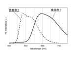
- 14 is an emission spectrum diagram of Example 1 and Comparative Example 1.
- FIG. 15 is an excitation spectrum diagram of Example 1 and Comparative Example 1.
- FIG. 16 is an afterglow spectrum diagram of Example 1 and Comparative Example 2.
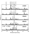
- FIG. 17 is an XRD diffraction pattern diagram of Examples 1 to 4 and Comparative Example 1.
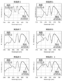
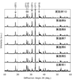
- FIG. 18 is a diagram showing emission spectra and excitation spectra of Examples 5 to 10.
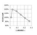
- FIG. 19 is a graph showing the relationship between Ce substitution concentration and relative light emission intensity in Examples 5 to 10.
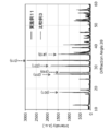
- 20 is an XRD diffraction pattern diagram of Examples 5 to 10 and Comparative Example 1.
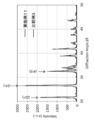
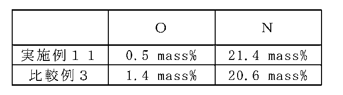
- FIG. 21A is an XRD diffraction pattern diagram of Example 11 and Comparative Example 3.
- FIG. 21B is an enlarged view of the XRD diffraction patterns of Example 11 and Comparative Example 3.
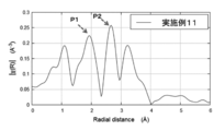
- FIG. 22 is a diagram showing a radial distribution function in the vicinity of Ce atoms in Example 11.
- FIG. 23 is a diagram showing a radial distribution function in the vicinity of Ce atoms in Comparative Example 3.
- the yellow phosphor YAG: Ce has high quantum efficiency of light emission, and since the quantum efficiency of light emission hardly changes even when excited by a high-power LED or LD, it is mounted on almost all white light sources.
- the red phosphor CASN: Eu has a problem that the quantum efficiency of light emission is lowered when excited with high output light, and is mounted only on a relatively low output light source. This is because a phosphor having an emission center of Eu has a longer emission lifetime than a phosphor having an emission center of Ce, so that the luminance is easily saturated at the time of high output excitation. Therefore, the present inventors have intensively studied to obtain a red phosphor having Ce as the emission center.
- Embodiment 1 The phosphor of Embodiment 1 contains a crystal phase having the chemical composition Ce x M 3-xy ⁇ 6 ⁇ 11-z . x satisfies 0 ⁇ x ⁇ 0.6. Since Ce needs to be included in order to obtain light emission, x is larger than 0. x is preferably 0.0003 or more, more preferably 0.015 or more, from the viewpoint of increasing the emission intensity. There is no particular limitation on the maximum value of x as long as the phosphor can emit light. However, when x becomes too large, the emission intensity decreases due to concentration quenching. Therefore, by setting x to 0.6 or less, it is possible to suppress a decrease in light emission intensity. Further, x is preferably 0.3 or less, more preferably 0.15 or less, from the viewpoint of increasing the emission intensity.
- M is another rare earth element not containing Ce. Specifically, it is one or more elements selected from the group consisting of Sc, Y, La, Pr, Nd, Sm, Eu, Gd, Tb, Dy, Ho, Er, Tm, Yb, and Lu. M may contain 90 mol% or more of La. Since the element group other than La has an ionic radius close to La, it can enter the M site.
- Y satisfies 0 ⁇ y ⁇ 1.0.
- y is larger than 1.0, the structure becomes unstable. Therefore, the structure can be stabilized by setting y to 1.0 or less.
- ⁇ contains 50 mol% or more of Si. That is, ⁇ is only Si or contains 50 mol% or more of Si and contains 50 mol% or less of other elements.
- ⁇ may include, for example, one or two elements selected from the group consisting of Al and Ga.
- (100x / 6) mol% or more of ⁇ may be one or two of these elements. That is, in Ce x M 3-xy ⁇ 6 ⁇ 11-z , the amount of one or two elements may be greater than or equal to the amount of Ce.
- (300 ⁇ / 6) mol% or more of ⁇ may be one or two of these elements. That is, in Ce x M 3-xy ⁇ 6 ⁇ 11-z , the amount of one or two elements may be three or more times the amount of Ce. ⁇ may further contain other elements as long as the phosphor can emit light.
- ⁇ contains 80 mol% or more of N. That is, ⁇ is only N or contains 80 mol% or more of N and contains 20 mol% or less of other elements. Further, ⁇ may contain, for example, O (oxygen). Thus, for example, when a part of the Si site in the vicinity of Ce is replaced with Al (or Ga), or a part of the N site is replaced with O, the symmetry of the Ce ligand is lowered and the length is longer. Light emission with a wavelength can be realized.
- Z satisfies 0 ⁇ z ⁇ 1.0.
- N is deficient (that is, when z is larger than 0), the symmetry of the Ce ligand becomes low, and longer wavelength light emission can be realized.
- z is larger than 1.0, the structure becomes unstable. Therefore, the structure can be stabilized by setting z to 1.0 or less.
- the phosphor of Embodiment 1 has the maximum peak of the emission spectrum at a wavelength of 600 nm to 800 nm.
- the maximum peak is a peak having the maximum value in the entire spectrum.
- the peak of the above-mentioned emission spectrum appears when excited at a wavelength of 535 nm, for example.
- the phosphor of Embodiment 1 has the first peak of the excitation spectrum at a wavelength of 500 nm to 600 nm. Moreover, the phosphor of the first embodiment may further have a second peak of the excitation spectrum at a wavelength of 350 nm or more and less than 500 nm. The first or second peak may be the maximum peak of the excitation spectrum.
- the 1 / e emission lifetime of the phosphor of Embodiment 1 may show a value of 100 ns or less.
- the light emission lifetime affects the luminance saturation characteristic.
- a phosphor containing Eu such as CASN: Eu which is a conventional red phosphor, has a longer emission lifetime than a phosphor containing Ce. Therefore, the phosphor containing Eu is likely to be saturated in luminance due to a decrease in quantum efficiency during high output excitation. Therefore, the phosphor of Embodiment 1 having Ce as the emission center is promising as a red phosphor having a high quantum efficiency even at a high output as compared with the conventional red phosphor.
- the crystal phase having the chemical composition Ce x M 3-xy ⁇ 6 ⁇ 11-z in the phosphor of Embodiment 1 may be a tetragonal crystal. Further, the crystal phase may include a region whose space group is P4bm (# 100). In addition, the above-described crystal phase in Embodiment 1 may have almost the same crystal structure as the crystal represented by the general formula La 3 Si 6 N 11 .
- the plane indices indicated by the diffraction peaks may be (001), (211), (310), (221), (311), and (410), respectively.
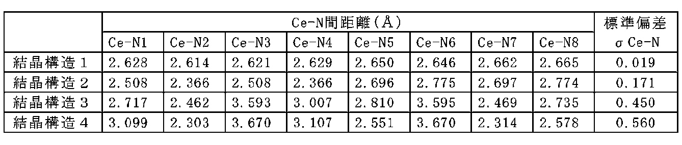
- the above-described crystal phase in Embodiment 1 may have the following characteristics in the XAFS measurement.
- the peak height of the first neighbor shell of Ce is lower than the peak height of the second neighbor shell of Ce. May be.
- the peak height of the first adjacent shell may be 0.8 times or more and 0.9 times or less the peak height of the second adjacent shell.
- the coordination number of the first adjacent shell of Ce obtained from the EXAFS radial distribution function spectrum at the K absorption edge of Ce may be seven coordination.
- the coordination structure in the vicinity of Ce is, for example, a structure in which nitrogen defects are introduced in the vicinity of the A site of La in La 3 Si 6 N 11 , and is a seven-coordinate coordination structure with low symmetry. Also good.
- a crystal represented by a conventional general formula La 3 Si 6 N 11 has an 8-coordinate coordination structure with high symmetry. Therefore, in the case of a seven-coordinate structure with low symmetry, the 5d orbital splitting is increased, and the energy difference from the 4f orbital is reduced, so that light emission with a longer wavelength than conventional can be realized.
- the above-described crystal phase may be a crystal phase represented by, for example, the chemical composition Ce x M 3-xy Si 6-q A q N 11-z .
- M is one or more elements selected from the group consisting of Sc, Y, La, Pr, Nd, Sm, Eu, Gd, Tb, Dy, Ho, Er, Tm, Yb, and Lu. May be.
- A may be one or two elements selected from the group consisting of Al and Ga. It may be 0 ⁇ x ⁇ 0.6. It may be 0 ⁇ y ⁇ 1.0. It may be 0 ⁇ z ⁇ 1.0. It may be x ⁇ q ⁇ 3.0.
- a method for manufacturing the phosphor according to the first embodiment will be described.
- the raw material for example, a compound containing Ce, La, Si, and Al (or Ga) may be used. Alternatively, each of Ce, La, Si, and Al (or Ga) alone may be used.
- the compound a compound that becomes a nitride by firing in a nitrogen atmosphere, a high-purity (purity 99% or more) nitride, a metal alloy, or the like can be used. In order to accelerate the reaction, a small amount of fluoride (such as ammonium fluoride) may be added.
- fluoride such as ammonium fluoride
- the chemical composition ratio is expressed as Ce x La 3-xy Si 6 N 11-z (0 ⁇ x ⁇ 0.6, 0 ⁇ y ⁇ 1.0, 0 ⁇ z ⁇ 1.0).
- a Ce compound, a La compound, and a Si compound (or Si simple substance) may be prepared, and an Al compound (or Al simple substance) may be further prepared.
- specific raw materials for example, CeF 3 powder (or CeN powder), LaN powder, Si 3 N 4 powder (or Si simple powder), and AlN powder (or Al simple powder) may be used.
- the LaN powder may be prepared in excess of about 24% from the theoretical value. Since LaN is easily decomposed at the time of firing, the formation of LaSi 3 N 5 crystals as a by-product can be suppressed by adding excessively at the time of blending the raw materials.
- the phosphor is manufactured by mixing and firing the above raw materials.
- the raw material mixing method may be wet mixing in a solution or dry mixing of a dry powder.
- Firing is performed for about 1 to 50 hours in a temperature range of 1500 to 2000 ° C. in an atmosphere pressurized with nitrogen.
- the pressure at this time is usually 3 atmospheres or more, desirably 4 atmospheres or more, and more desirably 8 atmospheres or more.
- the phosphor after firing may be washed, for example, in a nitric acid solution having a concentration of 10% for 1 hour.
- the obtained phosphor powder may be pulverized again using a ball mill, a jet mill or the like, and further washed or classified as necessary to adjust the particle size distribution or fluidity of the phosphor powder.
- Ce 3+ has one electron in the 4f orbit, which emits light when excited in the 5d orbit.
- the excited state of Ce is the 5d orbital
- the ground state is the 4f orbital
- the excitation-emission transition is the 4f-5d transition.
- Ce 3+ emits ultraviolet light in vacuum because of the large energy difference between 4f-5d.
- the present inventors examined a crystal in which the Ce ligand is asymmetric in order to increase the emission wavelength of the phosphor. As a result, as described later, the present inventors have found a crystal structure that is considered to have a ligand having lower symmetry than the Ce ligand in the conventional LSN: Ce yellow phosphor.
- the phosphor having the chemical composition of LSN: Ce disclosed in Patent Document 1, which is an example of a conventional LSN: Ce yellow phosphor has an emission peak wavelength of 574 nm to 594 nm and an excitation peak wavelength of 455 nm. ⁇ 460 nm.
- FIG. 3 shows the result of optimizing the structure of a La 3 Si 6 N 11 1 ⁇ 1 ⁇ 3 supercell.
- the space group of the unit cell of La 3 Si 6 N 11 is P4bm (# 100), and the coordination state of La includes an A site with high symmetry and a B site with low symmetry.
- FIG. 4 shows crystal structure 1 in which La at the A site is replaced with Ce and the structure is optimized.
- FIG. 5 shows a crystal structure 2 in which La at the B site is replaced with Ce and the structure is optimized.
- the crystal structure 2 in which La at the B site is replaced with Ce has lower symmetry of the Ce ligand than the crystal structure 1 in which La at the A site is replaced with Ce.
- the red phosphor of the first embodiment may contain Al as a starting material, there is a possibility that Al is taken into the crystal phase of the phosphor. Further, O may be incorporated into the phosphor crystal phase due to O contained in the raw material.
- Si and Al, and N and O have values of close ionic radii, and can be replaced. Further, when focusing on the ion radius, Al> Si, N> O. Therefore, replacing Si with Al increases the lattice constant, and replacing N with O decreases the lattice constant. That is, it is considered that crystals can exist more stably by simultaneously replacing Si with Al and N with O. Further, by simultaneously substituting Si for Al and N for O, the valence of the crystal can be maintained. Therefore, the number of moles of Al and O contained in the crystal phase may be the same.
- the amount of Al is preferably greater than the amount of Ce. Furthermore, since the charge compensation for N defects is possible by substituting three Si sites with Al, it is considered that the amount of Al is preferably three times or more of the amount of Ce.
- the above simulation results can be considered as an example of a factor in which the phosphor of Embodiment 1 exhibits red light emission on the longer wavelength side than the conventional LSN: Ce yellow phosphor. That is, the above simulation result is merely an example, and the crystal structure of the phosphor of Embodiment 1 is not limited at all.
- the phosphor according to Embodiment 1 can be used in a light emitting device.
- the light emitting device in this embodiment includes at least an excitation light source and a phosphor.
- the excitation light source emits light having a wavelength of 600 nm or less.
- the phosphor is the phosphor according to the first embodiment, which is irradiated with light emitted from the excitation light source and emits fluorescence having a longer wavelength than the light emitted from the excitation light source. According to the above configuration, a light emitting device with high quantum efficiency can be configured even at high output.
- the light emitted from the excitation light source may have a wavelength of 500 nm or more and 600 nm or less. Since the phosphor of Embodiment 1 typically has an excitation spectrum peak at a wavelength of 500 nm to 600 nm, it can be excited efficiently.
- the light emitted from the excitation light source may have a wavelength of 200 nm to 500 nm.
- the phosphor of Embodiment 1 has a wavelength that absorbs excitation light even at a wavelength of 500 nm or less.
- an excitation light source that emits light with a wavelength of 200 nm or more is desirable.
- LED or LD is mentioned, for example.
- the light emitting device in the present embodiment may further be combined with a second phosphor having an emission spectrum peak at a wavelength of 500 nm to 600 nm.
- the second phosphor emits fluorescence having a longer wavelength than the light emitted from the excitation light source when irradiated with the light emitted from the excitation light source.
- a phosphor containing a crystal phase may be used.
- the second phosphor may be a phosphor that emits yellow light, and a third phosphor that emits green light may be combined.
- the third phosphor emits fluorescence having a longer wavelength than the light emitted from the excitation light source when irradiated with the light emitted from the excitation light source.
- a phosphor containing a crystal phase of the chemical composition Lu 3 Al 5 O 12 : Ce (LuAG: Ce), or a chemical composition Y 3 (Al, Ga) 5 N 12: Ce (YAGG: A phosphor containing a crystal phase having Ce) may be used.
- Green light means light located in the range of (0.1 ⁇ x ⁇ 0.4, 0.5 ⁇ y ⁇ 0.8) in the CIE chromaticity coordinate values.
- Yellow light refers to light located in the range of (0.4 ⁇ x ⁇ 0.6, 0.4 ⁇ y ⁇ 0.6) in the CIE chromaticity coordinate values.
- the excitation light source and the second and third phosphors can be freely selected within the above-described range according to the use of the light emitting device. Therefore, the light emitting device including the phosphor according to Embodiment 1 is useful not only as a red light emitting device but also as a white light emitting device. Specifically, a combination of an excitation light source that emits blue light, a phosphor that emits yellow light, and the red phosphor of the present embodiment emits light in a high-color rendering high-output light-emitting device or light bulb color. A high-output light emitting device can be realized.
- Embodiment 2 demonstrates the LED light-emitting device which uses the LED chip as a light emitting element as a light source as an example of the light-emitting device of this indication.
- FIG. 8 is a schematic cross-sectional view showing an embodiment of the LED light-emitting device of Embodiment 2.
- the LED light emitting device 10 includes a phosphor 11, an LED chip 15, and an LED sealing body 24.
- FIG. The support body 23 supports the LED chip 15.
- the support 23 is a substrate.
- This embodiment can be used for a high-luminance LED light-emitting device.
- the support 23 has a high thermal conductivity so that heat generated in the LED chip 15 can be efficiently radiated to the outside.
- a ceramic substrate made of alumina or aluminum nitride can be used as the support 23.
- the LED chip 15 for example, one that emits light in the ultraviolet to yellow region is used, and one that has an emission spectrum peak at a wavelength of 200 nm to 600 nm is used. Specifically, a yellow LED chip, a green LED chip, a blue LED chip, a blue-violet LED chip, a near ultraviolet LED chip, an ultraviolet LED chip, or the like is used as the LED chip 15.
- the LED chip 15 is fixed to the support 23 with solder 27 or the like so that the emission surface 15 a does not come into contact with the support 23 on the support 23.
- the LED chip 15 is electrically connected to an electrode 22 provided on the support 23 by a bonding wire 21.
- the LED chip 15 is covered with an LED sealing body 24.
- a silicone resin is used for the LED sealing body 24.
- the phosphor 11 is dispersed in the LED sealing body 24.
- the silicone resin a silicone resin having a structure defined by various chemical formulas used as a sealing resin for a semiconductor light emitting device can be used.
- the silicone resin contains, for example, dimethyl silicone having high discoloration resistance.
- methylphenyl silicone etc. with high heat resistance can also be used as a silicone resin.
- the silicone resin may be a homopolymer having a main skeleton with a siloxane bond defined by one chemical formula.
- regulated by 2 or more types of chemical formula, and the alloy of 2 or more types of silicone polymers may be sufficient.
- the silicone resin in the LED sealing body 24 is in a state after being cured. Therefore, the LED sealing body 24 is also in a cured state.
- the LED sealing body 24 can be manufactured using an uncured silicone resin.
- the silicone resin is generally a two-component type in which curing is accelerated by mixing a main agent and a curing agent.
- a thermosetting silicone resin or an energy curable silicone resin that cures when irradiated with energy such as light can also be used.
- FIG. for example, an inorganic material made of ZnO such as glass or epoxy resin may be used.
- the phosphor 11 may be arranged on the LED sealing body 24 in the form of a phosphor plate without being dispersed in the LED sealing body 24.
- the LED chip is wire bonded, but the LED chip used in the present embodiment may have other configurations. That is, the LED chip used in the present embodiment may be mounted face-up or mounted by flip chip. Moreover, the LED chip used in the present embodiment may include a light emitting layer formed of a nitride semiconductor having a general polar plane (c-plane) growth surface.
- c-plane general polar plane
- the phosphor 11 absorbs a part of wavelength components or all wavelength components in the near ultraviolet to yellow region light (for example, near ultraviolet light) emitted from the LED chip 15 and emits fluorescence.
- the wavelength of light to be absorbed and the wavelength of fluorescence are determined by the type of fluorescent material contained in the phosphor 11.
- the phosphor 11 may be a mixed phosphor including a plurality of phosphors of different colors so that white light is created by the color mixture of light.
- the phosphor 11 may be a mixed phosphor of a green phosphor and a red phosphor. As the red phosphor, the phosphor of the first embodiment is used.
- the phosphor 11 may be a mixed phosphor of a yellow phosphor and a red phosphor.
- the red phosphor the phosphor of the first embodiment is used.
- the yellow phosphor include Y 3 Al 5 O 12 : Ce 3+ , CaSi 2 O 2 N 2 : Eu 2+ , (Ba, Sr) Si 2 O 2 N 2 : Eu 2+ , and Ca 3 Sc 2 Si 3 O.
- Phosphors such as 12 : Ce 3+ , CaSc 2 O 4 : Ce 3+ , ⁇ -SiAlON: Eu 2+ , La 3 Si 6 N 11 : Ce 3+ can be used.
- the particle diameter of the phosphor 11 is, for example, 1 ⁇ m or more and 80 ⁇ m or less, respectively.
- the particle diameter means a circle equivalent diameter measured by a microscopic method.
- the phosphor 11 is included in the LED sealing body 24 at a ratio of 3 parts by weight to 70 parts by weight with respect to 100 parts by weight of the sealing body, for example.
- the weight ratio of the phosphors that emit light of each color used in the phosphor 11 can be appropriately determined according to the desired color tone of white light and the emission intensity of each phosphor.
- the LED light emitting device is configured as an LED light emitting device that emits a color other than white by using only the red phosphor of the first embodiment or combining the phosphor 11 with another color phosphor. You can also.
- the above-described phosphors other than the red phosphor of Embodiment 1 can be manufactured according to a known method. Specifically, in the case of producing an oxide phosphor, as a raw material, a compound that becomes an oxide by firing, such as hydroxide, oxalate, or nitrate, or an oxide can be used. Here, in order to accelerate the reaction, a small amount of fluoride (for example, calcium fluoride) or chloride (for example, calcium chloride) can be added. The phosphor is manufactured by mixing and firing the above raw materials.
- the mixing method of the raw materials may be wet mixing in a solvent or dry mixing of dry powder.
- a ball mill, a medium stirring mill, a planetary mill, a vibration mill, a jet mill, a V-type mixer, a stirrer and the like that are usually used industrially can be used.
- the phosphor material is fired in the air or in a reducing atmosphere at a temperature range of 1100 to 1700 ° C. for about 1 to 50 hours.
- the furnace used for baking can use the furnace normally used industrially.
- a continuous or batch electric furnace such as a pusher furnace or a gas furnace, or a pressure firing furnace such as plasma sintering (SPS) or hot isostatic pressing (HIP) can be used.
- SPS plasma sintering
- HIP hot isostatic pressing
- FIG. 9 shows a schematic configuration of the LD light emitting device 60 according to the third embodiment.
- the LD light emitting device 60 includes an LD element 58 and a wavelength conversion member 61.
- the wavelength conversion member 61 includes a phosphor. The phosphor converts the light emitted from the LD element 58 into light having a longer wavelength.
- the LD element 58 can emit light having a higher optical power density than the LED. Therefore, the use of the LD element 58 can constitute a high-power LD light emitting device 60.
- the optical power density applied to the phosphor from the LD element 58 is, for example, 0.5 W / mm 2 or more. Further, the optical power density is irradiated onto the phosphor may also be 2W / mm 2 or more, may also be 3W / mm 2 or more, may be at 10 W / mm 2 or more.
- the light power density applied to the phosphor may be 150 W / mm 2 or less, 100 W / mm 2 or less, 50 W / mm 2 or less, or 20 W / mm 2. It may be the following.
- an element that emits light having a wavelength capable of exciting the phosphor can be used without particular limitation.
- an LD element that emits blue-violet light, an LD element that emits blue light, an LD element that emits green light, an LD element that emits yellow light, or the like can be used.
- blue light means light having a peak wavelength of 420 nm or more and less than 480 nm.
- the LD element 58 that emits blue light has higher luminous efficiency than the LD element that emits ultraviolet light, and has the highest luminous efficiency when the emission peak wavelength is 445 nm.
- the emission peak wavelength of the LD element 58 may be 425 nm or more, or 430 nm or more. On the other hand, the emission peak wavelength of the LD element 58 may be 475 nm or less, or 470 nm or less.
- the LD element 58 may be composed of one LD, or may be one in which a plurality of LDs are optically coupled.
- the LD element 58 may include a light emitting layer formed of a nitride semiconductor having a growth surface that is a nonpolar surface or a semipolar surface.
- the phosphor of the wavelength conversion member 61 includes the red phosphor of the first embodiment.
- the wavelength conversion member 61 may further include a phosphor other than the red phosphor of the first embodiment according to a desired emission color of the light emitting device.
- the LD light emitting device 60 can be configured as a white light emitting device.
- yellow fluorescent substance and green fluorescent substance what was illustrated in Embodiment 2 can be used.
- the wavelength conversion member 61 may be a single wavelength conversion layer in which a plurality of types of phosphors are mixed, and is a laminate in which at least two wavelength conversion layers including a single type or a plurality of types of phosphors are stacked. May be.
- the wavelength conversion member 61 having a configuration in which a first phosphor layer 62 composed of the red phosphor 12 and a second phosphor layer 63 composed of the yellow phosphor 13 are laminated. The case where is used will be described.
- the first phosphor layer 62 and the second phosphor layer 63 are configured using binders 68 and 69, respectively.
- the binders 68 and 69 are media, such as resin, glass, or a transparent crystal, for example.
- the binders 68 and 69 may be made of the same material or different materials.
- Each phosphor layer may be composed only of phosphor particles.
- An incident optical system 59 that guides the light of the LD element 58 to the second phosphor layer 63 may be provided between the wavelength conversion member 61 and the LD element 58.
- the incident optical system 59 includes, for example, a lens, a mirror, or an optical fiber.
- the blue light emitted from the LD element 58 passes through the incident optical system 59 and enters the second phosphor layer 63 of the wavelength conversion member 61.
- the plurality of yellow phosphors 13 of the second phosphor layer 63 are excited to emit yellow light.
- the blue light emitted from the LD element 58 that has been transmitted without being absorbed by the second phosphor layer 63 is incident on the first phosphor layer 62. Due to this incidence, the plurality of red phosphors 12 in the first phosphor layer 62 are excited and emit red light. Further, yellow light emitted from the second phosphor layer 63 is incident on the first phosphor layer 62.
- the plurality of red phosphors 12 of the first phosphor layer 62 may be excited by a part of the incident light to emit red light. Further, the blue light emitted from the LD element 58 that is transmitted without being absorbed by the first phosphor layer 62 and the second phosphor layer 63 is emitted to the outside. These red light, yellow light, and blue light are mixed to become white light.
- each phosphor layer may be adjusted so that the blue light emitted from the LD element 58 does not pass through the first phosphor layer 62. Further, it may be adjusted so that yellow light emitted from the second phosphor layer 63 does not pass through the first phosphor layer 62. In this case, only red light is emitted to the outside.
- the green phosphor described in the second embodiment may be used in place of the yellow phosphor 13 used in the second phosphor layer 63.
- FIG. 10 shows a schematic configuration of the LD light emitting device 80 according to the fourth embodiment.
- the LD light emitting device 80 includes an LD element 58 and a wavelength conversion member 81.
- the wavelength conversion member 81 includes a phosphor.
- the phosphor converts the light emitted from the LD element 58 into light having a longer wavelength.
- the phosphor of the wavelength conversion member 81 has a wavelength conversion layer in which the red phosphor 12 and at least one selected from the group consisting of the yellow phosphor 13 and the green phosphor 14 are mixed.
- the red phosphor 12 the phosphor of the first embodiment is used.
- yellow fluorescent substance and green fluorescent substance what was illustrated in Embodiment 2 can be used.
- the wavelength conversion member 81 is a phosphor layer formed by mixing three kinds of the red phosphor 12, the yellow phosphor 13, and the green phosphor 14 will be described.
- the mixing ratio of the three types of phosphors can be appropriately adjusted according to the desired color tone of white light, the emission intensity of each phosphor, and the like.
- the phosphor layer that is the wavelength conversion member 81 is configured using a binder 68.
- the binder 68 is a medium such as resin, glass, or transparent crystal.
- the binder 68 may be a single material or may be a different material depending on the location. Note that the phosphor layer may be composed of only phosphor particles.
- the blue light emitted from the LD element 58 passes through the incident optical system 59 and is red, yellow, and green light by the red phosphor 12, the yellow phosphor 13, and the green phosphor 14 in the wavelength conversion member 81, respectively. Is converted to The blue light emitted from the LD element 58 that is not absorbed by the phosphor is mixed with the red light, yellow light, and green light converted by the red phosphor 12, the yellow phosphor 13, and the green phosphor 14, respectively. White light.
- Embodiment 5 demonstrates an example of the illuminating device of this indication.
- FIG. 11 shows a schematic configuration of the illumination device 120 according to the fifth embodiment.
- the illumination device 120 includes a light source 121 and an output optical system 122 that guides light emitted from the light source 121 forward.
- a wavelength cut filter 123 that absorbs or reflects light from the light source may be provided.
- the light source 121 includes the red phosphor according to the first embodiment.
- the light source 121 may be the light emitting device 10, 60, or 80 of the second to fourth embodiments.
- the output optical system 122 may be a reflector, for example.
- the emission optical system 122 may include, for example, a metal film such as Al or Ag, or an Al film having a protective film formed on the surface.
- the quantum efficiency can be improved compared to the conventional illumination device at high output. Furthermore, when configured as a white illumination device, high color rendering and color reproducibility can be realized.
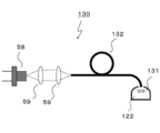
- FIG. 12 shows a schematic configuration of the illumination device 130 according to the sixth embodiment.
- the illumination device 130 includes an LD element 58, an incident optical system 59, an optical fiber 132, a wavelength conversion member 131, and an output optical system 122.
- the light emitted from the LD element 58 is guided to the optical fiber 132 through the incident optical system 59.
- the optical fiber 132 guides the light to the emission part.
- the emission unit includes, for example, a wavelength conversion member 131 and an emission optical system 122.
- the wavelength conversion member 131 includes the red phosphor according to the first embodiment. Further, the wavelength conversion member 131 may be the wavelength conversion member 61 or 81 of the third to fourth embodiments.
- the wavelength conversion member 131 may be positioned on the output side of the optical fiber 132 as shown in FIG. 12, but is on the incident side of the optical fiber 132 (for example, between the LD element 58 and the incident optical system 59, or (Between the incident optical system 59 and the optical fiber 132).
- the light irradiation direction can be easily changed by using an optical fiber.
- the red phosphor of the first embodiment is used, the quantum efficiency can be improved as compared with the conventional illumination device at the time of high output. Furthermore, when configured as a white illumination device, high color rendering and color reproducibility can be realized.
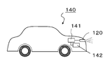
- FIG. 13 shows a schematic configuration of a vehicle 140 according to the seventh embodiment.
- the vehicle 140 includes a vehicle headlamp that is the illumination device 120 of the fifth embodiment, and a power supply source 141.
- the vehicle 140 may include a generator 142 that is rotated by a drive source such as an engine and generates electric power.
- the power generated by the generator 142 may be stored in the power supply source 141.
- the power supply source 141 may be a secondary battery that can be charged and discharged.
- the lighting device 120 is turned on by the power from the power supply source 141.
- the vehicle 140 is, for example, an automobile, a motorcycle, or a special vehicle.
- the vehicle 140 may be an engine vehicle, an electric vehicle, or a hybrid vehicle.
- the vehicle headlamp including the red phosphor of the first embodiment since the vehicle headlamp including the red phosphor of the first embodiment is used, it is possible to illuminate the front more brightly than before when the output is high. Furthermore, when configured as a white illumination device, high color rendering and color reproducibility can be realized.
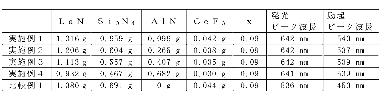
- Example 1 to 4 and Comparative Example 1 A method for manufacturing the phosphor is described below.
- LaN powder, Si 3 N 4 powder, AlN powder, and CeF 3 powder were prepared.
- LaN powder, Si 3 N 4 powder, and CeF 3 powder were weighed so as to have a composition represented by the general formula La 2.91 Ce 0.09 Si 6 N 11 and mixed.
- the LaN powder was weighed 24% more than the theoretical value.
- the amount of AlN powder shown in Table 2 was added to this mixed powder and further mixed.
- no AlN powder was added.
- dry mixing using a mortar was performed in a glove box under a nitrogen atmosphere.
- the mixed raw material powder was put in a crucible made of boron nitride. This raw material powder was fired at 1900 ° C. for 2 hours in a nitrogen atmosphere of 0.5 MPa. The calcined sample was washed in a nitric acid solution having a concentration of 10% for 1 hour.
- Examples 1 to 4 and Comparative Example 1 were prepared using starting materials as shown in Table 2.
- the emission spectra and excitation spectra of Examples 1 to 4 and Comparative Example 1 were measured using a spectrofluorometer (FP-6500 manufactured by JASCO Corporation).
- the emission spectra of Example 1 and Comparative Example 1 are shown in FIG. 14, and the excitation spectrum is shown in FIG.
- Table 2 shows emission peak wavelengths in the range of wavelengths from 450 nm to 800 nm and excitation peak wavelengths in the range of wavelengths from 400 nm to 600 nm.
- An Xe lamp was used as the excitation light source.
- the emission spectrum was measured using the excitation peak wavelength of each sample shown in Table 2 as the wavelength of the excitation light source.
- the excitation spectrum was measured using the emission peak wavelength of each sample shown in Table 2 as the monitor wavelength.
- Comparative Example 1 containing no AlN as a starting material showed yellow light emission with an emission peak wavelength of 536 nm.
- the excitation peak wavelength was 450 nm.
- a phosphor in which Ce is activated in a crystal represented by La 3 Si 6 N 11 has an emission peak on the short wavelength side (about 535 nm) and an emission peak on the long wavelength side (about 580 nm). ing. This substantially coincides with the emission peak on the short wavelength side and the emission peak on the long wavelength side in the phosphor of Patent Document 1. Further, the position of the excitation peak wavelength was almost the same as that of Patent Document 1.
- Examples 1 to 4 exhibited red light emission with an emission peak wavelength of about 640 nm. In Examples 1 to 4, it was found that there was an excitation peak at a wavelength of about 540 nm. From the above, it is clear that Examples 1 to 4 have different light emission characteristics from Comparative Example 1. In Examples 1 to 4, the excitation spectrum peak was further present at a wavelength of 350 nm or more and less than 500 nm.
- FIG. 16 shows an afterglow spectrum in which changes in emission intensity with respect to time after the excitation light is blocked are plotted for Example 1 and Comparative Example 2.
- Table 3 shows the 1 / e emission lifetimes of Examples 1 to 4 and Comparative Examples 1 and 2.
- the 1 / e emission lifetime of Example 1 was 54 ns. Further, in Examples 1 to 4 and Comparative Example 1, it was confirmed that the 1 / e emission lifetime was about 50 ns and showed a value of 100 ns or less. It is known that the light emission lifetime of Ce is generally about 10 ns to 100 ns. Therefore, the luminescence obtained from Examples 1 to 4 and Comparative Example 1 is considered to be derived from Ce.
- the light emission lifetime of CASN: Eu which is Comparative Example 2 was 820 ns.
- the light emission lifetime affects the luminance saturation characteristic. It is known that a phosphor containing Eu is more likely to be saturated in luminance due to a decrease in quantum efficiency during high-power excitation compared to a phosphor containing Ce.
- the phosphors of Examples 1 to 4 and Comparative Example 1 are considered to be less likely to be saturated with luminance because the emission lifetime value is significantly smaller than that of CASN: Eu. Therefore, the phosphors of Examples 1 to 4 and Comparative Example 1 can be combined with a high output excitation light source to realize a high output light emitting device.
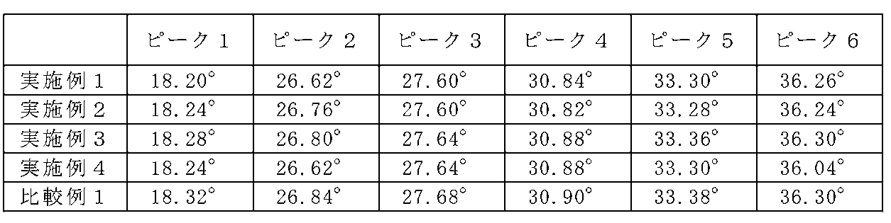
- the obtained X-ray diffraction pattern is shown in FIG. From FIG. 17, it can be seen that the X-ray diffraction patterns of Examples 1 to 4 are slightly shifted from the X-ray diffraction pattern obtained in Comparative Example 1 to the lower angle side, but almost coincide with each other. It was.
- diffraction peaks corresponding to the La 3 Si 6 N 11 crystal type are defined as peaks 1 to 6 from the low angle side, respectively, and 2 ⁇ values of the respective diffraction peaks are represented. As shown in FIG.
- the plane indices indicated by the peaks 1 to 6 were (001), (211), (310), (221), (311), and (410), respectively.
- the diffraction intensity of the diffraction peak corresponding to AlN or LaSi 3 N 5 becomes stronger as the charged amount of AlN increases.
- AlN it is considered that AlN at the time of blending remained unreacted.
- LaSi 3 N 5 it is considered that the LaSi 3 N 5 phase is easily generated by deviating from the stoichiometric composition of the La 3 Si 6 N 11 crystal.
- Example 1 The space group of the phosphor of Example 1 was analyzed using a single crystal X-ray structure analyzer (VariMax manufactured by Rigaku). As a result, it was found to be tetragonal. From this, it is considered that Examples 1 to 4 and Comparative Example 1 have almost the same crystal structure as the crystal represented by the general formula La 3 Si 6 N 11 .
- Example 5 to 10 A method for manufacturing the phosphor is described below.
- LaN powder, Si 3 N 4 powder, AlN powder, and CeN powder were prepared.
- LaN powder, Si 3 N 4 powder, and CeN powder were weighed so as to have a composition represented by the general formula La 3-x Ce x Si 6 N 11 and mixed.
- the LaN powder was weighed 24% more than the theoretical value.
- AlN powder was added to this mixed powder and further mixed.
- As a mixing method dry mixing using a mortar was performed in a glove box under a nitrogen atmosphere.
- the mixed raw material powder was put in a crucible made of boron nitride. This raw material powder was fired at 1900 ° C. for 2 hours in a nitrogen atmosphere of 0.5 MPa.
- the calcined sample was washed in a nitric acid solution having a concentration of 10% for 1 hour.
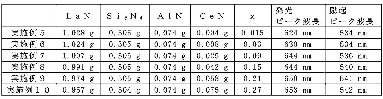
- Examples 5 to 10 were produced using starting materials as shown in Table 6.
- the emission spectra and excitation spectra of Examples 5 to 10 were measured using a spectrofluorometer (FP-6500 manufactured by JASCO). The emission spectra and excitation spectra of Examples 5 to 10 are shown in FIG. An Xe lamp was used as the excitation light source. The emission spectrum was measured using the excitation peak wavelength of each sample shown in Table 6 as the wavelength of the excitation light source. The excitation spectrum was measured using the emission peak wavelength of each sample shown in Table 6 as the monitor wavelength. In all the samples of Examples 5 to 10, red light emission having an emission peak wavelength at a wavelength of 600 nm or more was confirmed. The obtained emission peak wavelength was 624 nm to 653 nm.
- the excitation spectrum peak was further present at a wavelength of 350 nm or more and less than 500 nm.
- the internal quantum efficiency (IQE) of Examples 5 to 10 was measured using an absolute PL quantum yield measuring apparatus (C9920-02 manufactured by Hamamatsu Photonics).
- the relative luminescence intensity of Examples 5 to 10 is shown in FIG.
- the relative light emission intensity in this example is a relative value of each sample when the IQE of Example 5 is 100%.
- FIG. 19 shows that the relative emission intensity varies depending on the Ce concentration x in the phosphor.
- the Ce substitution concentration x in a range where the Ce substitution concentration x is higher than 0.03, the relative light emission intensity decreases as the Ce substitution concentration x increases. This is thought to be due to concentration quenching.
- it is necessary to include Ce so x is larger than 0.
- x is preferably 0.015 or more, for example.
- x is preferably 0.6 or less.
- x is, for example, preferably 0.3 or less, and more preferably 0.15 or less. For example, it was shown that a phosphor having higher emission intensity can be realized by setting the Ce substitution concentration x within the above range.
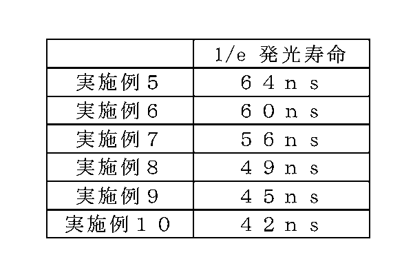
- Examples 5 to 10 it was confirmed that all 1 / e emission lifetimes showed values of 100 ns or less. Therefore, the phosphors of Examples 5 to 10 can be combined with a high output excitation light source to realize a high output light emitting device.
- the Ce concentration increases, energy transfer between adjacent Ce is likely to occur, and energy migration occurs. If electrons are trapped by defects in the crystal while energy migration occurs, they are relaxed as non-radiative transitions. That is, as the Ce concentration increases, it is considered that the light emission lifetime is shortened because the probability that an electron having a relatively low transition probability becomes non-emission (non-radiative transition) increases.
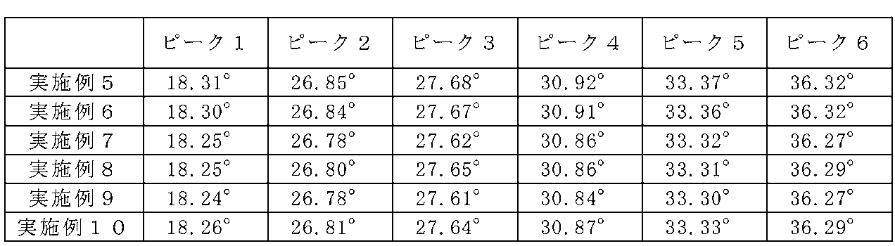
- FIG. 20 shows the obtained X-ray diffraction pattern.
- the X-ray diffraction patterns of Examples 5 to 10 were slightly shifted to the low angle side with respect to the X-ray diffraction pattern obtained in Comparative Example 1, it was found that they almost coincided.
- diffraction peaks corresponding to the La 3 Si 6 N 11 crystal type are defined as peaks 1 to 6 from the low angle side, respectively, and 2 ⁇ values of the respective diffraction peaks are represented. 9 shows.
- the plane indices indicated by the peaks 1 to 6 were (001), (211), (310), (221), (311), and (410), respectively. From these results, the space groups of the phosphors of Examples 5 to 10 are tetragonal, as in Examples 1 to 4 and Comparative Example 1, and crystals represented by the general formula La 3 Si 6 N 11 It is thought that they have almost the same crystal structure.
- Example 11 and Comparative Example 3 A method for manufacturing the phosphor is described below.
- LaN powder, Si 3 N 4 powder, AlN powder, and CeN powder were prepared.
- LaN powder, Si 3 N 4 powder, and CeN powder were weighed so as to have a composition represented by the general formula La 3-x Ce x Si 6 N 11 and mixed.
- the LaN powder was weighed 24% more than the theoretical value.
- AlN powder was added to this mixed powder and further mixed.
- As a mixing method dry mixing using a mortar was performed in a glove box under a nitrogen atmosphere.
- the mixed raw material powder was put in a crucible made of boron nitride. This raw material powder was fired at 1900 ° C. for 2 hours in a nitrogen atmosphere of 0.5 MPa.
- the calcined sample was washed in a 3% strength hydrochloric acid solution for 24 hours.
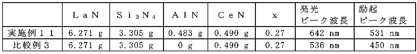
- Example 11 and Comparative Example 3 were produced using the starting materials as shown in Table 10.
- Example 11 red light emission having an emission peak wavelength at a wavelength of 600 nm or more was confirmed. Moreover, it was confirmed that it has an excitation peak wavelength at a wavelength of 500 nm or more.
- Example 11 and Comparative Example 3 were measured with a fluorescence lifetime measurement apparatus (Quantaurus-Tau small fluorescence lifetime measurement apparatus manufactured by Hamamatsu Photonics). Table 11 shows the 1 / e emission lifetimes of Example 11 and Comparative Example 3.
- Example 11 it was confirmed that the 1 / e emission lifetime shows a value of 100 ns or less.
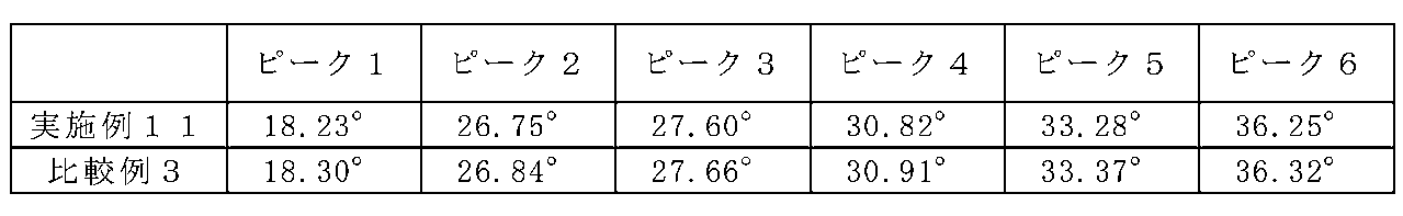
- Example 11 It was found that the X-ray diffraction pattern of Example 11 almost coincided with the X-ray diffraction pattern obtained in Comparative Example 3. Moreover, it turned out that each X-ray-diffraction peak in Example 11 is slightly shifted to the low angle side compared with each X-ray-diffraction peak in Comparative Example 3.
- diffraction peaks corresponding to the La 3 Si 6 N 11 crystal type are defined as peaks 1 to 6 from the low angle side, respectively, and 2 ⁇ values of the respective diffraction peaks are represented. 12 shows.
- the plane indices indicated by the peaks 1 to 6 were (001), (211), (310), (221), (311), and (410), respectively. From these results, the space group of the phosphor of Example 11 is tetragonal as in Examples 1 to 10 and Comparative Examples 1 and 3, and is represented by the general formula La 3 Si 6 N 11. It is thought that it has almost the same crystal structure as the crystal.
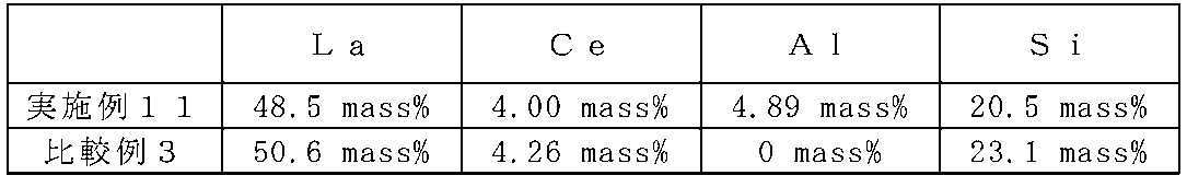
- Example 11 and Comparative Example 3 Composition analysis of Example 11 and Comparative Example 3 was performed by measurement using inductively coupled plasma spectroscopy (ICP-AES). The pretreatment for measurement is shown below. After alkali melting using sodium peroxide, the melt was dissolved in hydrochloric acid, diluted with pure water, and the Si content was analyzed. Further, alkali fusion was performed using lithium tetraborate and sodium carbonate, the melt was dissolved in hydrochloric acid, diluted with pure water, and the contents of La, Al, and Ce were analyzed. The results are shown in Table 13.
- ICP-AES inductively coupled plasma spectroscopy
- Example 11 contained Al.
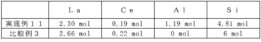
- Table 14 shows the molar ratio of each element when the total amount of Al and Si is converted to 6 mol.
- Table 14 shows that the total amount of La and Ce in the samples of Example 11 and Comparative Example 3 is less than the stoichiometric composition (3 mol). This is thought to be because LaN and CeN, which are starting materials, were decomposed during firing. Thus, as long as light can be emitted, La and Ce may be less than the stoichiometric composition. For example, the total content of La and Ce may be 2 mol or more and 3 mol or less.
- Example 11 and Comparative Example 3 were melted in an inert gas at 2300 ° C., the amount of oxygen was measured by the non-dispersive infrared absorption method (NDIR), and the amount of nitrogen was measured by the thermal conductivity method (TCD). .
- NDIR non-dispersive infrared absorption method
- TCD thermal conductivity method
- Example 11 contained O.
- O may be contained as long as light can be emitted. Since it is difficult to absolutely quantify anions and cations at the same time, the absolute values of the contents of each element shown in Tables 13 to 15 include errors. Therefore, the composition of the phosphor of the present disclosure is not limitedly interpreted by the absolute value of the content of each element shown in Tables 13 to 15.
- Table 16 shows the parameters used in the analysis.
- FIG. 22 shows a graph of the radial distribution function of Example 11.
- FIG. 23 shows a graph of the radial distribution function of Comparative Example 3.
- the horizontal axis of the radial distribution function corresponds to the distance to neighboring atoms.
- the vertical axis (peak height) indicates the coordination number n. 22 and 23, the peak near 1.1 ⁇ is a ghost peak due to noise in the measurement signal.
- the peak (P1) near 1.9% is the peak of the first adjacent shell of Ce.
- the peak (P2) near 2.6 ⁇ is the peak of the second adjacent shell of Ce.
- the peak near 3.3 ⁇ is the peak of the third adjacent shell of Ce.
- the height of the peak (P1) of the first adjacent shell is higher than the height of the peak (P2) of the second adjacent shell.
- the height of the peak (P1) of the first adjacent shell is lower than the height of the peak (P2) of the second adjacent shell (approximately 0.84 times).
- the height of P2 of Example 11 is substantially equal to the height of P2 of Comparative Example 3.
- the height of P1 of Example 11 is clearly lower than the height of P1 of Comparative Example 3.
- the coordination structure in the vicinity of Ce in Comparative Example 3 is a structure in which eight nitrogen atoms are coordinated as in the La A site in La 3 Si 6 N 11 and has a relatively high symmetry. It turned out to be. Further, the coordination structure in the vicinity of Ce in Example 11 is a structure in which a nitrogen defect is introduced in the vicinity of the A site of La in La 3 Si 6 N 11 , and is a seven-coordinate coordination structure with low symmetry. It turned out to be.
- Example 11 since the symmetry of the coordination structure in the vicinity of Ce was lowered due to the Frenkel defect or the like, the 5d orbital splitting was increased and the energy difference from the 4f orbital was thought to be reduced. Therefore, it is considered that a Ce-based phosphor that emits red light with a longer emission wavelength can be realized.
- the phosphors of Examples 1 to 11 have almost the same crystal structure as the crystal represented by the general formula La 3 Si 6 N 11 , they exhibit red emission on the longer wavelength side than the conventional LSN: Ce yellow phosphor. It was. The reason for this is not necessarily clear, but for example, the following possibilities are conceivable. Unlike the conventional case, the phosphors of Examples 1 to 11 may contain red light emission because Al (for example, AlN powder) is included in the raw material.
- Al for example, AlN powder
- the phosphor of the present disclosure is useful as a light emitting device.
- general lighting devices such as ceiling lights, spotlights, special lighting devices such as stadium lighting and studio lighting
- vehicle lighting devices such as headlamps
- projectors such as projectors and head-up displays
- endoscope lights Light source in imaging devices such as digital cameras, mobile phones, smart phones, personal computer (PC) monitors, notebook personal computers, televisions, personal digital assistants (PDX), smart phones, tablet PCs, mobile phones, etc.
- imaging devices such as digital cameras, mobile phones, smart phones, personal computer (PC) monitors, notebook personal computers, televisions, personal digital assistants (PDX), smart phones, tablet PCs, mobile phones, etc.
- PDX personal digital assistants
- smart phones tablet PCs, mobile phones, etc.
Abstract
Description
黄色蛍光体YAG:Ceは、発光の量子効率が高く、また高出力LEDあるいはLDで励起しても発光の量子効率がほとんど変化しないため、ほぼ全ての白色光源に搭載されている。一方、赤色蛍光体CASN:Euは、高出力光で励起すると発光の量子効率が低下するという問題があり、比較的低出力の光源にしか搭載されていない。これは、Euを発光中心とした蛍光体は、Ceを発光中心とした蛍光体と比較して発光寿命が長いため、高出力励起時に輝度飽和しやすいためである。そこで、本発明者らは、Ceを発光中心とした赤色蛍光体を得るべく、鋭意研究した。
実施形態1の蛍光体は、化学組成CexM3-x-yβ6γ11-zを有する結晶相を含有する。xは、0<x≦0.6を満たす。発光を得るためにCeを含む必要があるため、xは0より大きい。xは、発光強度増大の観点から、望ましくは0.0003以上、より望ましくは0.015以上である。蛍光体が発光し得る限りxの最大値に特に制限はない。しかし、xが大きくなりすぎる場合には、濃度消光により発光強度が低下する。そのため、xを0.6以下とすることにより、発光強度の低下を抑制できる。また、xは、発光強度増大の観点から、望ましくは0.3以下、より望ましくは0.15以下である。
以下、実施形態1の蛍光体の製造方法について説明する。原料としては、例えば、Ce、La、Si、およびAl(またはGa)を含有する化合物を用いてもよい。または、Ce、La、Si、およびAl(またはGa)それぞれの単体を用いてもよい。化合物としては、窒素雰囲気下での焼成により窒化物になる化合物、高純度(純度99%以上)の窒化物、金属合金、などを用いることができる。また、反応を促進するために、フッ化物(フッ化アンモニウム等)を少量添加してもよい。
以下に、本発明者らが、実施形態1の蛍光体の結晶構造について、シミュレーションを交えて検討した結果を示す。Ce3+は4f軌道に1つの電子を有し、これが5d軌道に励起されることで発光が起きる。また、Ce3+を発光中心とする蛍光体においては、Ceの励起状態は5d軌道、基底状態は4f軌道であり、励起-発光遷移は4f-5d遷移である。Ce3+は、真空中においては4f-5d間のエネルギー差が大きいため紫外発光する。
実施形態1の蛍光体は、発光装置に利用されうる。本実施形態における発光装置は、励起光源と、蛍光体と、を少なくとも備える。励起光源は、波長600nm以下の光を発する。蛍光体は、励起光源の発する光を照射され、励起光源の発する光よりも長波長の蛍光を発する、実施形態1の蛍光体である。以上の構成によれば、高出力時においても量子効率の高い発光装置を構成することができる。
実施形態2では、本開示の発光装置の一例として、発光素子としてのLEDチップを光源とするLED発光装置について説明する。図8は、実施形態2のLED発光装置の一実施形態を示す模式的な断面図である。図8に示すように、LED発光装置10は、蛍光体11と、LEDチップ15と、LED封止体24と、を備える。また、支持体23を備えてもよい。支持体23は、LEDチップ15を支持する。本実施形態では、LED発光装置10は、面実装が可能な構造を備えているため、支持体23は基板である。
蛍光体11は、LEDチップ15から出射される近紫外から黄色領域の光(例えば、近紫外光)のうち、一部の波長成分、あるいは、すべての波長成分を吸収し、蛍光を発する。吸収する光の波長および蛍光の波長は、蛍光体11に含まれる蛍光材料の種類によって決まる。蛍光体11は、光の混色により白色光が作り出されるように、複数の異なる色の蛍光体を含む混合蛍光体であってもよい。蛍光体11は、緑色蛍光体および赤色蛍光体の混合蛍光体であってもよい。赤色蛍光体としては、実施形態1の蛍光体が用いられる。
実施形態3では、本開示の発光装置の一例として、発光素子としてのLDを光源とするLD発光装置について説明する。図9は、実施形態3に係るLD発光装置60の概略構成を示している。LD発光装置60は、LD素子58と、波長変換部材61と、を備える。波長変換部材61は、蛍光体を含む。蛍光体は、LD素子58からの出射光を、より長波長の光に波長変換する。
実施形態4では、本開示の発光装置の一例として、発光素子としてのLDを光源とするLD発光装置について説明する。図10は、実施形態4に係るLD発光装置80の概略構成を示している。実施形態3と同一の部材については、同一の符号を付してその説明を省略する。LD発光装置80は、LD素子58と、波長変換部材81と、を備える。
実施形態5では、本開示の照明装置の一例について説明する。図11は、実施形態5に係る照明装置120の概略構成を示している。照明装置120は、光源121と、光源121が発する光を前方に導く出射光学系122と、を備える。光源からの発光色を調整するために、光源からの光を吸収又は反射する波長カットフィルター123を設けてもよい。光源121は、実施形態1の赤色蛍光体を含む。また、光源121は、実施形態2~4の発光装置10、60または80であってもよい。出射光学系122は、例えば、リフレクタであってもよい。出射光学系122は、例えば、AlまたはAgなどの金属膜、または、表面に保護膜が形成されたAl膜を有してもよい。
実施形態6では、本開示の照明装置の一例として、光ファイバーを用いた照明装置について説明する。図12は、実施形態6に係る照明装置130の概略構成を示している。照明装置130は、LD素子58と、入射光学系59と、光ファイバー132と、波長変換部材131と、出射光学系122と、を備える。
実施形態7では、本開示の照明装置の応用例として、照明装置を備えた車両について説明する。図13は、実施形態7に係る車両140の概略構成を示している。車両140は、実施形態5の照明装置120である車両用ヘッドランプと、電力供給源141と、を備える。また、車両140は、エンジン等の駆動源によって回転駆動され、電力を発生する発電機142を有してもよい。発電機142が生成した電力は、電力供給源141に蓄えられてもよい。電力供給源141は、充放電が可能な2次電池であってもよい。照明装置120は、電力供給源141からの電力によって点灯する。車両140は、例えば、自動車、2輪車又は特殊車両である。また、車両140は、エンジン車、電気車、又はハイブリッド車であってもよい。
蛍光体の作製方法を以下に示す。出発原料として、LaN粉末、Si3N4粉末、AlN粉末、CeF3粉末を用意した。まず、LaN粉末とSi3N4粉末とCeF3粉末を、一般式La2.91Ce0.09Si6N11で表される組成となるように秤量し、それらを混合した。ただし、LaN粉末は、理論値よりも24%過剰に秤量した。この混合粉末にAlN粉末を表2に示す量を加え、更に混合した。なお、比較例1では、AlN粉末は加えなかった。混合の方法としては、窒素雰囲気下のグローブボックス中で、乳鉢を用いた乾式混合を行った。混合した原料粉末を窒化ホウ素製の坩堝に入れた。この原料粉末を、0.5MPaの窒素雰囲気中で1900℃にて2時間焼成した。焼成後の試料を濃度10%の硝酸溶液中で1時間洗浄した。以上の方法により、表2に示したような出発原料で、実施例1~4および比較例1を作製した。
出発原料として、Ca3N2粉末、Si3N4粉末、AlN粉末、EuN粉末を用意した。Ca3N2粉末とSi3N4粉末とAlN粉末とEuN粉末を一般式Ca0.97Eu0.03AlSiN3で表される組成となるように秤量し、それらを混合した。混合の方法としては、窒素雰囲気下のグローブボックス中で、乳鉢を用いた乾式混合を行った。混合した原料粉末を窒化ホウ素製の坩堝に入れた。この原料粉末を0.5MPaの窒素雰囲気中で1600℃にて2時間焼成した。焼成後の試料を濃度10%の硝酸溶液中で1時間洗浄した。以上の方法により、CASN:Euで表される、比較例2を作製した。
実施例1~4および比較例1の発光スペクトルと励起スペクトルを、分光蛍光光度計(日本分光製FP-6500)を用いて測定した。実施例1および比較例1の発光スペクトルを図14に、励起スペクトルを図15に示す。また、波長450nmから波長800nmの範囲の発光ピーク波長と、波長400nmから波長600nmの範囲の励起ピーク波長を表2に示す。なお、励起光源にはXeランプを用いた。表2に示す各試料の励起ピーク波長を励起光源の波長として、発光スペクトルを測定した。表2に示す各試料の発光ピーク波長をモニター波長として、励起スペクトルを測定した。
実施例1~4および比較例1および比較例2の発光寿命を、蛍光寿命測定装置(浜松ホトニクス製Quantaurus-Tau小型蛍光寿命測定装置)により測定した。図16に、励起光を遮断した後の時間に対する発光強度の変化をプロットした残光スペクトルを、実施例1および比較例2について示す。また、表3に、実施例1~4および比較例1および比較例2の1/e発光寿命を示す。

実施例1~4および比較例1の粉末X線回折パターンを、X線回折測定装置(Rigaku製RINT2100)を用いて測定した。測定には、Cu-Kα線を用い、表4に示す条件で行った。

蛍光体の作製方法を以下に示す。出発原料として、LaN粉末、Si3N4粉末、AlN粉末、CeN粉末を用意した。まず、LaN粉末とSi3N4粉末とCeN粉末を、一般式La3-xCexSi6N11で表される組成となるように秤量し、それらを混合した。ただし、LaN粉末は、理論値よりも24%過剰に秤量した。この混合粉末にAlN粉末を加えて更に混合した。混合の方法としては、窒素雰囲気下のグローブボックス中で、乳鉢を用いた乾式混合を行った。混合した原料粉末を窒化ホウ素製の坩堝に入れた。この原料粉末を、0.5MPaの窒素雰囲気中で1900℃にて2時間焼成した。焼成後の試料を濃度10%の硝酸溶液中で1時間洗浄した。以上の方法により、表6に示したような出発原料で、実施例5~10を作製した。
実施例5~10の発光スペクトルと励起スペクトルを、分光蛍光光度計(日本分光製FP-6500)を用いて測定した。実施例5~10の発光スペクトルおよび励起スペクトルを図18に示す。なお、励起光源にはXeランプを用いた。表6に示す各試料の励起ピーク波長を励起光源の波長として、発光スペクトルを測定した。表6に示す各試料の発光ピーク波長をモニター波長として、励起スペクトルを測定した。実施例5~10の全ての試料において、波長600nm以上に発光ピーク波長を有する赤色発光が確認された。なお、得られた発光ピーク波長は、624nm~653nmであった。
実施例5~10の内部量子効率(IQE)を、絶対PL量子収率測定装置(浜松ホトニクス製C9920-02)を用いて測定した。実施例5~10の相対発光強度を図19に示す。ここで、本実施例における相対発光強度とは、実施例5のIQEを100%とした場合の、各試料の相対値である。
実施例5~10の発光寿命を、蛍光寿命測定装置(浜松ホトニクス製Quantaurus-Tau小型蛍光寿命測定装置)により測定した。表7に、実施例5~10の1/e発光寿命を示す。
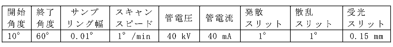
実施例5~10および比較例1の粉末X線回折パターンを、X線回折測定装置(Rigaku製RINT2100)を用いて測定した。測定には、Cu-Kα線を用い、表8に示す条件で行った。
蛍光体の作製方法を以下に示す。出発原料として、LaN粉末、Si3N4粉末、AlN粉末、CeN粉末を用意した。まず、LaN粉末とSi3N4粉末とCeN粉末を、一般式La3-xCexSi6N11で表される組成となるように秤量し、それらを混合した。ただし、LaN粉末は、理論値よりも24%過剰に秤量した。この混合粉末にAlN粉末を加え、更に混合した。混合の方法としては、窒素雰囲気下のグローブボックス中で、乳鉢を用いた乾式混合を行った。混合した原料粉末を窒化ホウ素製の坩堝に入れた。この原料粉末を、0.5MPaの窒素雰囲気中で1900℃にて2時間焼成した。焼成後の試料を濃度3%の塩酸溶液中で24時間洗浄した。以上の方法により、表10に示したような出発原料で、実施例11および比較例3を作製した。
実施例11および比較例3の発光寿命を、蛍光寿命測定装置(浜松ホトニクス製Quantaurus-Tau小型蛍光寿命測定装置)により測定した。表11に、実施例11および比較例3の1/e発光寿命を示す。

実施例11および比較例3の粉末X線回折パターンを、X線回折測定装置(Rigaku製RINT2100)を用いて測定した。測定には、Cu-Kα線を用い、上述の表8に示す条件で行った。得られたX線回折パターンを、図21Aおよび図21Bに示す。
誘導結合プラズマ分光分析法(ICP-AES)を用いた測定により、実施例11および比較例3の組成分析を行った。測定の前処理を以下に示す。過酸化ナトリウムを用いてアルカリ融解を行い、融成物を塩酸で溶解した後、純水で希釈し、Siの含有量を分析した。また、四ホウ酸リチウムと炭酸ナトリウムを用いてアルカリ融解を行い、融成物を塩酸で溶解した後、純水で希釈し、LaとAlとCeの含有量を分析した。その結果を表13に示す。
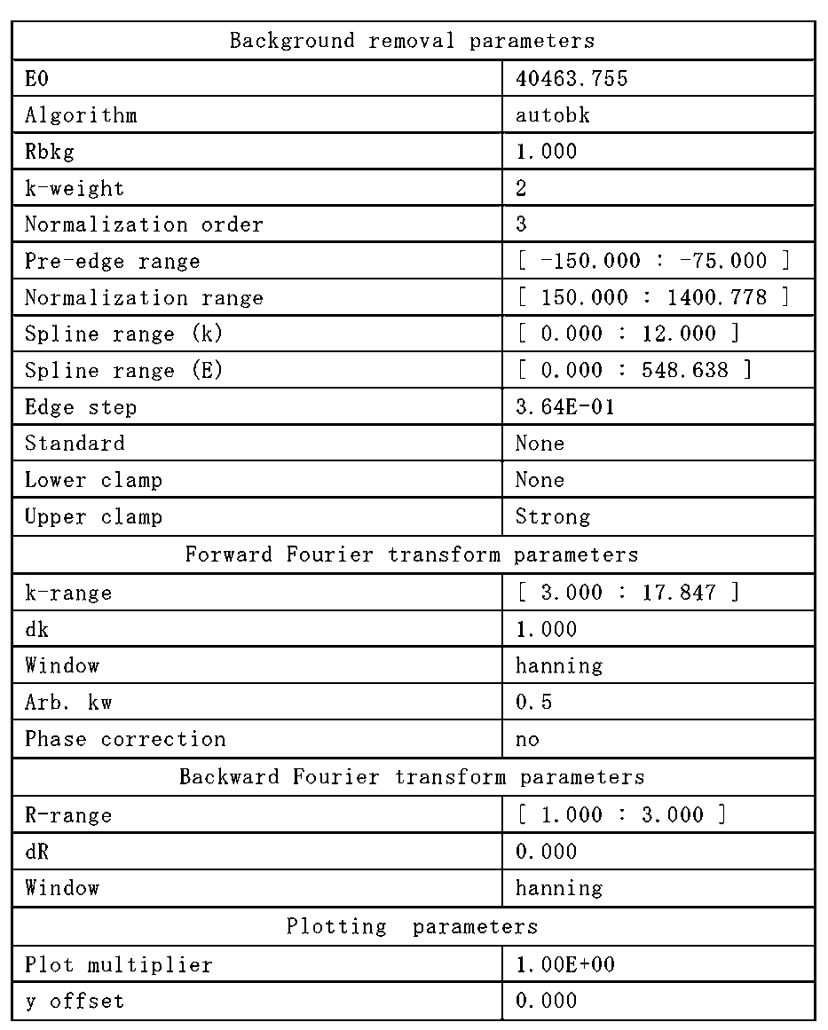
実施例11および比較例3のCe配位子の局所構造をX線吸収微細構造分析(XAFS)により測定した。XAFS測定は、国立研究開発法人理化学研究所、SPring8のビームライン16B2を用いて行った。
11 蛍光体
12 赤色蛍光体
13 黄色蛍光体
14 緑色蛍光体
15 LEDチップ
21 ボンディングワイヤ
22 電極
23 支持体
24 LED封止体
27 半田
58 LD素子
59 入射光学系
60 LD発光装置
61 波長変換部材
62 第1の蛍光体層
63 第2の蛍光体層
68 バインダー
69 バインダー
80 LD発光装置
81 波長変換部材
120 照明装置
121 光源
122 出射光学系
123 波長カットフィルター
130 照明装置
131 波長変換部材
132 光ファイバー
140 車両
141 電力供給源
142 発電機
Claims (22)
- 化学組成CexM3-x-yβ6γ11-zを有する結晶相を含有し、
Mは、Sc、Y、La、Pr、Nd、Sm、Eu、Gd、Tb、Dy、Ho、Er、Tm、Yb、Luからなる群より選ばれる一種または二種以上の元素であり、
βは、Siを50モル%以上含み、
γは、Nを80モル%以上含み、
0<x≦0.6であり、
0≦y≦1.0であり、
0≦z≦1.0であり、
波長600nm以上800nm以下に発光スペクトルの最大ピークを有し、
波長500nm以上600nm以下に励起スペクトルの第一のピークを有する、
蛍光体。 - 前記Mは、Laを90モル%以上含む、
請求項1に記載の蛍光体。 - 前記βは、AlおよびGaからなる群より選ばれる一種または二種の元素をさらに含む、
請求項1または2に記載の蛍光体。 - 前記βの(100x/6)モル%以上は、前記一種または二種の元素である、
請求項3に記載の蛍光体。 - 前記γは、Oをさらに含む、
請求項1から4のいずれかに記載の蛍光体。 - 前記xは、0.015≦x≦0.3を満たす、
請求項1から5のいずれかに記載の蛍光体。 - 波長350nm以上500nm未満に前記励起スペクトルの第二のピークを有する、
請求項1から6のいずれかに記載の蛍光体。 - 前記第一または第二のピークは前記励起スペクトルの最大ピークである請求項7に記載の蛍光体。
- 前記結晶相の1/e発光寿命が100ns以下である、
請求項1から8のいずれかに記載の蛍光体。 - Cu-Kα線で測定したX線回折パターンにおいて、
2θ=17.8°以上18.8°以下、
2θ=26.2°以上27.2°以下、
2θ=27.2°以上28.2°以下、
2θ=30.5°以上31.5°以下、
2θ=32.8°以上33.8°以下、および、
2θ=35.8°以上36.8°以下、に回折ピークを有する結晶相を含有する、
請求項1から9のいずれかに記載の蛍光体。 - CeのK吸収端のEXAFS動径分布関数スペクトルにおいて、Ceの第一近接殻のピークの高さが、Ceの第二近接殻のピークの高さよりも低い、
請求項1から10のいずれかに記載の蛍光体。 - 化学組成CexM3-x-yβ6γ11-zを有する結晶相を含有し、
Mは、Sc、Y、La、Pr、Nd、Sm、Eu、Gd、Tb、Dy、Ho、Er、Tm、Yb、Luからなる群より選ばれる一種または二種以上の元素であり、
βは、Siを50モル%以上含み、
γは、Nを80モル%以上含み、
0<x≦0.6であり、
0≦y≦1.0であり、
0≦z≦1.0であり、
CeのK吸収端のEXAFS動径分布関数スペクトルにおいて、Ceの第一近接殻のピークの高さが、Ceの第二近接殻のピークの高さよりも低い、
蛍光体。 - 前記第一近接殻のピークの高さが、前記第二近接殻のピークの高さの0.8倍以上0.9倍以下である、
請求項11または12に記載の蛍光体。 - CeのK吸収端のEXAFS動径分布関数スペクトルから得られる、Ceの第一近接殻の配位数が7配位である、
請求項1から13のいずれかに記載の蛍光体。 - 化学組成CexM3-x-yβ6γ11-zを有する結晶相を含有し、
Mは、Sc、Y、La、Pr、Nd、Sm、Eu、Gd、Tb、Dy、Ho、Er、Tm、Yb、Luからなる群より選ばれる一種または二種以上の元素であり、
βは、Siを50モル%以上含み、
γは、Nを80モル%以上含み、
0<x≦0.6であり、
0≦y≦1.0であり、
0≦z≦1.0であり、
CeのK吸収端のEXAFS動径分布関数スペクトルから得られる、Ceの第一近接殻の配位数が7配位である、
蛍光体。 - 前記yは0であり、前記zは0である、請求項1から15のいずれかに記載の蛍光体。
- 波長600nm以下の光を発する励起光源と、
前記励起光源の発する光を照射され、前記光よりも長波長の蛍光を発する、請求項1から16のいずれかに記載の蛍光体と、を備える、
発光装置。 - 前記励起光源は、波長500nm以上600nm以下の光を発する、
請求項17に記載の発光装置。 - 前記励起光源は、波長420nm以上480nm以下の光を発する、
請求項17に記載の発光装置。 - 前記励起光源は、LEDまたはLDである、
請求項17から19のいずれかに記載の発光装置。 - 前記蛍光体を第一の蛍光体とし、
前記励起光源の発する光を照射され、前記光よりも長波長の蛍光を発する、第二の蛍光体をさらに備え、
前記第二の蛍光体は、波長500nm以上600nm以下に発光スペクトルの最大ピークを有する、
請求項17から20のいずれかに記載の発光装置。 - 前記第二の蛍光体は、黄色光を発する蛍光体であり、
前記励起光源の発する光を照射され、緑色光を発する第三の蛍光体をさらに備える、
請求項21に記載の発光装置。
Priority Applications (32)
| Application Number | Priority Date | Filing Date | Title |
|---|---|---|---|
| JP2017518363A JP6206696B1 (ja) | 2016-07-04 | 2017-01-13 | 蛍光体および発光装置 |
| KR1020177016121A KR102635866B1 (ko) | 2016-07-04 | 2017-01-13 | 형광체 및 발광 장치 |
| EP17734219.3A EP3480280B1 (en) | 2016-07-04 | 2017-01-13 | Fluorophore and light-emitting device |
| CN201780000449.XA CN108138045B (zh) | 2016-07-04 | 2017-01-13 | 荧光体以及发光装置 |
| PCT/JP2017/019464 WO2018008281A1 (ja) | 2016-07-04 | 2017-05-25 | 蛍光体および発光装置 |
| JP2017539670A JP6281801B1 (ja) | 2016-07-04 | 2017-05-25 | 蛍光体および発光装置 |
| CN201780002095.2A CN107851950B (zh) | 2016-07-04 | 2017-05-25 | 光纤光源、内窥镜以及内窥镜系统 |
| JP2017554414A JP6273637B1 (ja) | 2016-07-04 | 2017-05-25 | ファイバー光源、内視鏡および内視鏡システム |
| CN201780001107.XA CN107849448B (zh) | 2016-07-04 | 2017-05-25 | 荧光体以及发光装置 |
| JP2017554415A JP6264706B1 (ja) | 2016-07-04 | 2017-05-25 | プロジェクター装置 |
| EP17823890.3A EP3480903B1 (en) | 2016-07-04 | 2017-05-25 | Fiber light source, endoscope, and endoscope system |
| PCT/JP2017/019466 WO2018008283A1 (ja) | 2016-07-04 | 2017-05-25 | ファイバー光源、内視鏡および内視鏡システム |
| KR1020177026995A KR20190028628A (ko) | 2016-07-04 | 2017-05-25 | 형광체 및 발광 장치 |
| KR1020177036015A KR102324696B1 (ko) | 2016-07-04 | 2017-05-25 | 형광체를 이용한 발광 장치 |
| PCT/JP2017/019465 WO2018008282A1 (ja) | 2016-07-04 | 2017-05-25 | 蛍光体を用いた発光装置 |
| EP17823891.1A EP3480904B1 (en) | 2016-07-04 | 2017-05-25 | Projector device |
| PCT/JP2017/019467 WO2018008284A1 (ja) | 2016-07-04 | 2017-05-25 | プロジェクター装置 |
| CN201780002085.9A CN108028304B (zh) | 2016-07-04 | 2017-05-25 | 使用了荧光体的发光装置 |
| EP17780614.8A EP3480281A4 (en) | 2016-07-04 | 2017-05-25 | FLUORESCENT SUBSTANCE AND LIGHT EMITTING DEVICE |
| EP17823889.5A EP3480863B1 (en) | 2016-07-04 | 2017-05-25 | Light-emitting device using fluorophore |
| CN201780002084.4A CN107851949B (zh) | 2016-07-04 | 2017-05-25 | 投影机装置 |
| JP2017554413A JP6340749B2 (ja) | 2016-07-04 | 2017-05-25 | 蛍光体を用いた発光装置 |
| US15/636,747 US10214429B2 (en) | 2016-07-04 | 2017-06-29 | Phosphor containing Ce |
| US15/723,240 US10955114B2 (en) | 2016-07-04 | 2017-10-03 | Phosphor and light-emitting apparatus |
| JP2017236202A JP6887092B2 (ja) | 2016-07-04 | 2017-12-08 | プロジェクター装置 |
| JP2017245126A JP6917881B2 (ja) | 2016-07-04 | 2017-12-21 | ファイバー光源、内視鏡および内視鏡システム |
| JP2018002590A JP2018131605A (ja) | 2016-07-04 | 2018-01-11 | 蛍光体および発光装置 |
| US15/933,455 US10714661B2 (en) | 2016-07-04 | 2018-03-23 | Light-emitting apparatus including phosphor |
| US15/933,624 US11036120B2 (en) | 2016-07-04 | 2018-03-23 | Projector including phosphor |
| US15/933,606 US11149198B2 (en) | 2016-07-04 | 2018-03-23 | Fiber light source including phosphor |
| JP2018086215A JP6893320B2 (ja) | 2016-07-04 | 2018-04-27 | 蛍光体を用いた発光装置 |
| US16/245,101 US10717657B2 (en) | 2016-07-04 | 2019-01-10 | Phosphor containing Ce |
Applications Claiming Priority (2)
| Application Number | Priority Date | Filing Date | Title |
|---|---|---|---|
| JP2016-132126 | 2016-07-04 | ||
| JP2016132126 | 2016-07-04 |
Related Child Applications (5)
| Application Number | Title | Priority Date | Filing Date |
|---|---|---|---|
| PCT/JP2017/019467 Continuation-In-Part WO2018008284A1 (ja) | 2016-07-04 | 2017-05-25 | プロジェクター装置 |
| PCT/JP2017/019465 Continuation-In-Part WO2018008282A1 (ja) | 2016-07-04 | 2017-05-25 | 蛍光体を用いた発光装置 |
| PCT/JP2017/019464 Continuation WO2018008281A1 (ja) | 2016-07-04 | 2017-05-25 | 蛍光体および発光装置 |
| PCT/JP2017/019466 Continuation-In-Part WO2018008283A1 (ja) | 2016-07-04 | 2017-05-25 | ファイバー光源、内視鏡および内視鏡システム |
| US15/636,747 Continuation US10214429B2 (en) | 2016-07-04 | 2017-06-29 | Phosphor containing Ce |
Publications (1)
| Publication Number | Publication Date |
|---|---|
| WO2018008171A1 true WO2018008171A1 (ja) | 2018-01-11 |
Family
ID=60912452
Family Applications (1)
| Application Number | Title | Priority Date | Filing Date |
|---|---|---|---|
| PCT/JP2017/000935 WO2018008171A1 (ja) | 2016-07-04 | 2017-01-13 | 蛍光体および発光装置 |
Country Status (5)
| Country | Link |
|---|---|
| EP (1) | EP3480280B1 (ja) |
| JP (1) | JP2018021198A (ja) |
| KR (1) | KR102635866B1 (ja) |
| CN (1) | CN108138045B (ja) |
| WO (1) | WO2018008171A1 (ja) |
Cited By (5)
| Publication number | Priority date | Publication date | Assignee | Title |
|---|---|---|---|---|
| JP2019104894A (ja) * | 2017-12-08 | 2019-06-27 | パナソニックIpマネジメント株式会社 | 蛍光体および発光装置 |
| WO2020153260A1 (ja) * | 2019-01-25 | 2020-07-30 | パナソニックIpマネジメント株式会社 | 蛍光体、波長変換部材及び発光装置 |
| CN111885953A (zh) * | 2018-03-28 | 2020-11-03 | 松下知识产权经营株式会社 | 内窥镜用发光装置及使用了该发光装置的内窥镜以及荧光成像方法 |
| JP2020198397A (ja) * | 2019-06-04 | 2020-12-10 | 日亜化学工業株式会社 | 発光装置の製造方法 |
| JPWO2020162243A1 (ja) * | 2019-02-04 | 2021-12-09 | パナソニックIpマネジメント株式会社 | 発光装置及びそれを用いた医療装置 |
Families Citing this family (1)
| Publication number | Priority date | Publication date | Assignee | Title |
|---|---|---|---|---|
| JP7111995B2 (ja) * | 2020-05-18 | 2022-08-03 | 日亜化学工業株式会社 | 蛍光体組成物およびその製造方法 |
Citations (6)
| Publication number | Priority date | Publication date | Assignee | Title |
|---|---|---|---|---|
| JP3837588B2 (ja) | 2003-11-26 | 2006-10-25 | 独立行政法人物質・材料研究機構 | 蛍光体と蛍光体を用いた発光器具 |
| JP2007231245A (ja) * | 2005-05-24 | 2007-09-13 | National Institute For Materials Science | 蛍光体及びその利用 |
| JP2008533233A (ja) * | 2005-03-08 | 2008-08-21 | コーニンクレッカ フィリップス エレクトロニクス エヌ ヴィ | 放射線源とルミネッセンス材料を含む照明システム |
| JP2008285606A (ja) * | 2007-05-18 | 2008-11-27 | Nec Lighting Ltd | 蛍光体、その製造方法及び発光装置 |
| JP4459941B2 (ja) | 2006-10-04 | 2010-04-28 | 三菱化学株式会社 | 蛍光体及びその製造方法、並びに、蛍光体含有組成物、発光装置、画像表示装置及び照明装置 |
| JP2014224230A (ja) * | 2013-04-26 | 2014-12-04 | 日亜化学工業株式会社 | 蛍光体及びそれを用いた発光装置並びに蛍光体の製造方法 |
Family Cites Families (9)
| Publication number | Priority date | Publication date | Assignee | Title |
|---|---|---|---|---|
| JP4466757B2 (ja) * | 2007-04-18 | 2010-05-26 | 三菱化学株式会社 | 蛍光体、蛍光体含有組成物、発光装置、照明装置、画像表示装置、及び窒素含有化合物 |
| CN102361956B (zh) * | 2009-03-31 | 2014-10-29 | 三菱化学株式会社 | 荧光体、荧光体的制造方法、含荧光体组合物、发光装置、照明装置和图像显示装置 |
| WO2012017949A1 (ja) * | 2010-08-04 | 2012-02-09 | 宇部興産株式会社 | 珪窒化物蛍光体用窒化珪素粉末並びにそれを用いたCaAlSiN3系蛍光体、Sr2Si5N8系蛍光体、(Sr,Ca)AlSiN3系蛍光体及びLa3Si6N11系蛍光体、及びその製造方法 |
| JP2013028667A (ja) * | 2011-07-27 | 2013-02-07 | Panasonic Corp | イットリウムアルミニウムガーネットタイプの蛍光体とこれを用いた発光装置 |
| KR101873221B1 (ko) * | 2011-12-09 | 2018-07-06 | 삼성전자주식회사 | 형광체 및 발광장치 |
| WO2014074349A1 (en) * | 2012-11-07 | 2014-05-15 | The Regents Of The University Of California | White light source employing a iii-nitride based laser diode pumping a phosphor |
| JP6123619B2 (ja) * | 2013-09-30 | 2017-05-10 | 住友大阪セメント株式会社 | 複合波長変換粒子及び複合波長変換粒子含有樹脂組成物並びに発光装置 |
| US9331253B2 (en) * | 2014-09-03 | 2016-05-03 | Cree, Inc. | Light emitting diode (LED) component comprising a phosphor with improved excitation properties |
| JPWO2016092743A1 (ja) * | 2014-12-12 | 2017-11-24 | パナソニックIpマネジメント株式会社 | 発光装置 |
-
2017
- 2017-01-13 EP EP17734219.3A patent/EP3480280B1/en active Active
- 2017-01-13 WO PCT/JP2017/000935 patent/WO2018008171A1/ja active Application Filing
- 2017-01-13 CN CN201780000449.XA patent/CN108138045B/zh active Active
- 2017-01-13 KR KR1020177016121A patent/KR102635866B1/ko active IP Right Grant
- 2017-08-22 JP JP2017159333A patent/JP2018021198A/ja active Pending
Patent Citations (6)
| Publication number | Priority date | Publication date | Assignee | Title |
|---|---|---|---|---|
| JP3837588B2 (ja) | 2003-11-26 | 2006-10-25 | 独立行政法人物質・材料研究機構 | 蛍光体と蛍光体を用いた発光器具 |
| JP2008533233A (ja) * | 2005-03-08 | 2008-08-21 | コーニンクレッカ フィリップス エレクトロニクス エヌ ヴィ | 放射線源とルミネッセンス材料を含む照明システム |
| JP2007231245A (ja) * | 2005-05-24 | 2007-09-13 | National Institute For Materials Science | 蛍光体及びその利用 |
| JP4459941B2 (ja) | 2006-10-04 | 2010-04-28 | 三菱化学株式会社 | 蛍光体及びその製造方法、並びに、蛍光体含有組成物、発光装置、画像表示装置及び照明装置 |
| JP2008285606A (ja) * | 2007-05-18 | 2008-11-27 | Nec Lighting Ltd | 蛍光体、その製造方法及び発光装置 |
| JP2014224230A (ja) * | 2013-04-26 | 2014-12-04 | 日亜化学工業株式会社 | 蛍光体及びそれを用いた発光装置並びに蛍光体の製造方法 |
Non-Patent Citations (3)
| Title |
|---|
| LIU,LIHONG ET AL.: "Yellow-Emitting Y3Si6N11: Ce3+ Phosphorus for White Light-Emitting Diodes(LEDs", JOURNAL OF THE AMERICAN CERAMIC SOCIETY, vol. 96, no. 6, June 2013 (2013-06-01), pages 1688 - 1690, XP055450326 * |
| See also references of EP3480280A1 |
| ZHU,QIANG-QIANG ET AL.: "Extra-Broad Band Orange-Emitting Ce3+-Doped Y3Si5N90 Phosphor for Solid-State Lighting: Electronic, Crystal Structures and Luminescence Properties", CHEMISTRY OF MATERIALS, vol. 28, 20 June 2016 (2016-06-20), pages 4829 - 4839, XP055450320 * |
Cited By (9)
| Publication number | Priority date | Publication date | Assignee | Title |
|---|---|---|---|---|
| JP2019104894A (ja) * | 2017-12-08 | 2019-06-27 | パナソニックIpマネジメント株式会社 | 蛍光体および発光装置 |
| JP7108841B2 (ja) | 2017-12-08 | 2022-07-29 | パナソニックIpマネジメント株式会社 | 蛍光体および発光装置 |
| CN111885953A (zh) * | 2018-03-28 | 2020-11-03 | 松下知识产权经营株式会社 | 内窥镜用发光装置及使用了该发光装置的内窥镜以及荧光成像方法 |
| CN111885953B (zh) * | 2018-03-28 | 2023-11-07 | 松下知识产权经营株式会社 | 内窥镜用发光装置及使用了该发光装置的内窥镜以及荧光成像方法 |
| WO2020153260A1 (ja) * | 2019-01-25 | 2020-07-30 | パナソニックIpマネジメント株式会社 | 蛍光体、波長変換部材及び発光装置 |
| JPWO2020162243A1 (ja) * | 2019-02-04 | 2021-12-09 | パナソニックIpマネジメント株式会社 | 発光装置及びそれを用いた医療装置 |
| JP7390599B2 (ja) | 2019-02-04 | 2023-12-04 | パナソニックIpマネジメント株式会社 | 発光装置及びそれを用いた医療装置 |
| JP2020198397A (ja) * | 2019-06-04 | 2020-12-10 | 日亜化学工業株式会社 | 発光装置の製造方法 |
| JP7319528B2 (ja) | 2019-06-04 | 2023-08-02 | 日亜化学工業株式会社 | 発光装置の製造方法 |
Also Published As
| Publication number | Publication date |
|---|---|
| JP2018021198A (ja) | 2018-02-08 |
| EP3480280B1 (en) | 2022-09-07 |
| EP3480280A4 (en) | 2019-07-31 |
| KR102635866B1 (ko) | 2024-02-13 |
| KR20190024557A (ko) | 2019-03-08 |
| CN108138045B (zh) | 2022-04-26 |
| EP3480280A1 (en) | 2019-05-08 |
| CN108138045A (zh) | 2018-06-08 |
Similar Documents
| Publication | Publication Date | Title |
|---|---|---|
| JP6206696B1 (ja) | 蛍光体および発光装置 | |
| JP6340749B2 (ja) | 蛍光体を用いた発光装置 | |
| WO2018008171A1 (ja) | 蛍光体および発光装置 | |
| US11001753B2 (en) | Phosphor that includes cerium | |
| EP3495448B1 (en) | Phosphor and light-emitting apparatus | |
| JP6281801B1 (ja) | 蛍光体および発光装置 | |
| US10662376B2 (en) | Phosphor that includes crystal phase containing celium |
Legal Events
| Date | Code | Title | Description |
|---|---|---|---|
| ENP | Entry into the national phase |
Ref document number: 2017518363 Country of ref document: JP Kind code of ref document: A |
|
| ENP | Entry into the national phase |
Ref document number: 20177016121 Country of ref document: KR Kind code of ref document: A |
|
| REEP | Request for entry into the european phase |
Ref document number: 2017734219 Country of ref document: EP |
|
| 121 | Ep: the epo has been informed by wipo that ep was designated in this application |
Ref document number: 17734219 Country of ref document: EP Kind code of ref document: A1 |
|
| NENP | Non-entry into the national phase |
Ref country code: DE |