WO2017204159A1 - 被処理体を処理する方法 - Google Patents
被処理体を処理する方法 Download PDFInfo
- Publication number
- WO2017204159A1 WO2017204159A1 PCT/JP2017/019024 JP2017019024W WO2017204159A1 WO 2017204159 A1 WO2017204159 A1 WO 2017204159A1 JP 2017019024 W JP2017019024 W JP 2017019024W WO 2017204159 A1 WO2017204159 A1 WO 2017204159A1
- Authority
- WO
- WIPO (PCT)
- Prior art keywords
- layer
- film
- gas
- mask
- processed
- Prior art date
- Legal status (The legal status is an assumption and is not a legal conclusion. Google has not performed a legal analysis and makes no representation as to the accuracy of the status listed.)
- Ceased
Links
Images




Classifications
-
- H—ELECTRICITY
- H10—SEMICONDUCTOR DEVICES; ELECTRIC SOLID-STATE DEVICES NOT OTHERWISE PROVIDED FOR
- H10P—GENERIC PROCESSES OR APPARATUS FOR THE MANUFACTURE OR TREATMENT OF DEVICES COVERED BY CLASS H10
- H10P50/00—Etching of wafers, substrates or parts of devices
- H10P50/20—Dry etching; Plasma etching; Reactive-ion etching
- H10P50/24—Dry etching; Plasma etching; Reactive-ion etching of semiconductor materials
- H10P50/242—Dry etching; Plasma etching; Reactive-ion etching of semiconductor materials of Group IV materials
-
- H—ELECTRICITY
- H10—SEMICONDUCTOR DEVICES; ELECTRIC SOLID-STATE DEVICES NOT OTHERWISE PROVIDED FOR
- H10P—GENERIC PROCESSES OR APPARATUS FOR THE MANUFACTURE OR TREATMENT OF DEVICES COVERED BY CLASS H10
- H10P50/00—Etching of wafers, substrates or parts of devices
- H10P50/73—Etching of wafers, substrates or parts of devices using masks for insulating materials
-
- C—CHEMISTRY; METALLURGY
- C09—DYES; PAINTS; POLISHES; NATURAL RESINS; ADHESIVES; COMPOSITIONS NOT OTHERWISE PROVIDED FOR; APPLICATIONS OF MATERIALS NOT OTHERWISE PROVIDED FOR
- C09K—MATERIALS FOR MISCELLANEOUS APPLICATIONS, NOT PROVIDED FOR ELSEWHERE
- C09K13/00—Etching, surface-brightening or pickling compositions
-
- H—ELECTRICITY
- H10—SEMICONDUCTOR DEVICES; ELECTRIC SOLID-STATE DEVICES NOT OTHERWISE PROVIDED FOR
- H10P—GENERIC PROCESSES OR APPARATUS FOR THE MANUFACTURE OR TREATMENT OF DEVICES COVERED BY CLASS H10
- H10P14/00—Formation of materials, e.g. in the shape of layers or pillars
- H10P14/60—Formation of materials, e.g. in the shape of layers or pillars of insulating materials
-
- H—ELECTRICITY
- H10—SEMICONDUCTOR DEVICES; ELECTRIC SOLID-STATE DEVICES NOT OTHERWISE PROVIDED FOR
- H10P—GENERIC PROCESSES OR APPARATUS FOR THE MANUFACTURE OR TREATMENT OF DEVICES COVERED BY CLASS H10
- H10P50/00—Etching of wafers, substrates or parts of devices
- H10P50/20—Dry etching; Plasma etching; Reactive-ion etching
- H10P50/26—Dry etching; Plasma etching; Reactive-ion etching of conductive or resistive materials
- H10P50/264—Dry etching; Plasma etching; Reactive-ion etching of conductive or resistive materials by chemical means
- H10P50/266—Dry etching; Plasma etching; Reactive-ion etching of conductive or resistive materials by chemical means by vapour etching only
- H10P50/267—Dry etching; Plasma etching; Reactive-ion etching of conductive or resistive materials by chemical means by vapour etching only using plasmas
-
- H—ELECTRICITY
- H10—SEMICONDUCTOR DEVICES; ELECTRIC SOLID-STATE DEVICES NOT OTHERWISE PROVIDED FOR
- H10P—GENERIC PROCESSES OR APPARATUS FOR THE MANUFACTURE OR TREATMENT OF DEVICES COVERED BY CLASS H10
- H10P50/00—Etching of wafers, substrates or parts of devices
- H10P50/20—Dry etching; Plasma etching; Reactive-ion etching
- H10P50/28—Dry etching; Plasma etching; Reactive-ion etching of insulating materials
- H10P50/282—Dry etching; Plasma etching; Reactive-ion etching of insulating materials of inorganic materials
- H10P50/283—Dry etching; Plasma etching; Reactive-ion etching of insulating materials of inorganic materials by chemical means
-
- H—ELECTRICITY
- H10—SEMICONDUCTOR DEVICES; ELECTRIC SOLID-STATE DEVICES NOT OTHERWISE PROVIDED FOR
- H10P—GENERIC PROCESSES OR APPARATUS FOR THE MANUFACTURE OR TREATMENT OF DEVICES COVERED BY CLASS H10
- H10P74/00—Testing or measuring during manufacture or treatment of wafers, substrates or devices
- H10P74/20—Testing or measuring during manufacture or treatment of wafers, substrates or devices characterised by the properties tested or measured, e.g. structural or electrical properties
- H10P74/203—Structural properties, e.g. testing or measuring thicknesses, line widths, warpage, bond strengths or physical defects
-
- H—ELECTRICITY
- H10—SEMICONDUCTOR DEVICES; ELECTRIC SOLID-STATE DEVICES NOT OTHERWISE PROVIDED FOR
- H10P—GENERIC PROCESSES OR APPARATUS FOR THE MANUFACTURE OR TREATMENT OF DEVICES COVERED BY CLASS H10
- H10P74/00—Testing or measuring during manufacture or treatment of wafers, substrates or devices
- H10P74/23—Testing or measuring during manufacture or treatment of wafers, substrates or devices characterised by multiple measurements, corrections, marking or sorting processes
-
- H—ELECTRICITY
- H10—SEMICONDUCTOR DEVICES; ELECTRIC SOLID-STATE DEVICES NOT OTHERWISE PROVIDED FOR
- H10P—GENERIC PROCESSES OR APPARATUS FOR THE MANUFACTURE OR TREATMENT OF DEVICES COVERED BY CLASS H10
- H10P76/00—Manufacture or treatment of masks on semiconductor bodies, e.g. by lithography or photolithography
- H10P76/40—Manufacture or treatment of masks on semiconductor bodies, e.g. by lithography or photolithography of masks comprising inorganic materials
- H10P76/408—Manufacture or treatment of masks on semiconductor bodies, e.g. by lithography or photolithography of masks comprising inorganic materials characterised by their sizes, orientations, dispositions, behaviours or shapes
- H10P76/4085—Manufacture or treatment of masks on semiconductor bodies, e.g. by lithography or photolithography of masks comprising inorganic materials characterised by their sizes, orientations, dispositions, behaviours or shapes characterised by the processes involved to create the masks
-
- H—ELECTRICITY
- H10—SEMICONDUCTOR DEVICES; ELECTRIC SOLID-STATE DEVICES NOT OTHERWISE PROVIDED FOR
- H10P—GENERIC PROCESSES OR APPARATUS FOR THE MANUFACTURE OR TREATMENT OF DEVICES COVERED BY CLASS H10
- H10P95/00—Generic processes or apparatus for manufacture or treatments not covered by the other groups of this subclass
- H10P95/90—Thermal treatments, e.g. annealing or sintering
Definitions
- Embodiments described herein relate generally to a method for processing an object to be processed.
- a mask is formed on a layer to be processed, and etching is performed to transfer the pattern of the mask to the layer to be processed.
- a resist mask is generally used as a mask.
- the resist mask is formed by a photolithography technique. Therefore, the critical dimension of the pattern formed on the layer to be etched is affected by the resolution limit of the resist mask formed by photolithography technology, the pattern density, etc., but in recent years, along with the higher integration of electronic devices. Therefore, it is required to form a pattern having a size smaller than the resolution limit of the resist mask. Therefore, as described in Patent Document 1, by forming a silicon oxide film on a resist mask, the size of the resist mask is adjusted, and the width of the opening provided by the resist mask is reduced. Has been proposed.
- a photoresist pattern is formed on a material film on which a fine pattern is to be formed, and a silicon oxide film is deposited thereon, but the underlying photoresist pattern is damaged. It must be conformally thin without adding. Thereafter, dry etching is performed on the lower film. Initially, a spacer is formed on the sidewall of the photoresist pattern, and then a polymer film is formed on the photoresist pattern.
- a method for treating a workpiece is provided.
- a to-be-processed object is provided with the mask provided in the to-be-processed layer and the main surface of a to-be-processed layer.
- This method includes a first step of adjusting the groove width of the mask pattern, and a second step of etching the layer to be processed using the mask after the execution of the first step.
- the main surface is divided into a plurality of regions in the method, and the first step includes a third step and a third step of measuring a groove width value for each of the plurality of regions divided in the method.
- the fourth step of calculating the positive difference value obtained by subtracting the reference value of the groove width from the value of the groove width measured in the third step for each of a plurality of regions, and the execution of the fourth step A fifth step of forming a film having a difference film thickness for each of the plurality of regions calculated in the fourth step on the surface of the mask of the object to be processed carried into the processing container of the plasma processing apparatus; .
- the fifth step includes a sixth step for supplying the first gas into the processing vessel, a seventh step for purging the inside of the processing vessel after the execution of the sixth step, and after the execution of the seventh step.
- the processing time required in the sixth step is within the time during which the film thickness of the film deposited on the surface of the mask on the target layer in the sixth step increases or decreases depending on the temperature of the target layer.
- the first gas can contain an aminosilane-based gas
- the second gas can contain a gas containing oxygen atoms and carbon atoms.
- the first step of adjusting the groove width of the mask pattern is performed before the second step of etching the layer to be processed.
- the main surface of the layer to be processed is divided into a plurality of regions, and in the third step and the fourth step, the difference value between the groove width of the mask and the reference value of the groove width is determined for each of the plurality of regions.
- the fifth step a film having a film thickness corresponding to the difference value is formed on the mask, and the groove width of the mask is corrected to the reference value for each of a plurality of regions.
- a film is formed on the mask for each atomic layer by a method similar to the ALD (Atomic Layer Deposition) method using a film forming process that repeatedly executes the sixth to ninth steps.
- the tenth process uses correspondence data indicating the correspondence between the temperature of the layer to be processed and the film thickness of the film to be formed.
- the temperature of the layer to be processed is adjusted so as to be a temperature necessary for forming a film having a film thickness corresponding to the difference value calculated in the fourth step.
- the film thickness corresponding to the correction amount of the mask groove is determined for each of the plurality of regions of the main surface of the processing target layer, and is necessary for the formation of the film thickness. Since the temperature of the layer to be processed is determined using the corresponding data, and the temperature of the layer to be processed is adjusted at the temperature determined for each of the plurality of regions, the film forming process similar to the ALD method is performed. Variations in the mask pattern can be suppressed in detail and sufficiently for each of a plurality of regions of the main surface of the layer to be processed.
- the temperature of each of the plurality of regions in the processing layer of the target object carried into the processing container is the difference value calculated for each of the plurality of regions in the fourth step.
- the temperature of the layer to be processed is adjusted for each of the plurality of regions based on the correspondence data so that the temperature corresponds to the film thickness.
- the fifth step includes a twelfth step of forming a film conformally on the surface of the mask without depending on a plurality of regions, and the tenth step is carried into the processing container.
- the film thickness of the film formed conformally in the twelfth step from the film thickness of the difference value calculated for each of the plurality of regions in the fourth step with respect to the temperature of the plurality of regions in the layer to be processed.
- the temperature of the layer to be processed is adjusted for each of the plurality of regions based on the corresponding data so that the temperature corresponds to the value obtained by subtracting the value, and the twelfth step is performed before the tenth step or after the film formation processing. Done.
- the film can be partially formed without adjusting the temperature of the layer to be processed performed for each of the plurality of regions.
- the third step and the fourth step are re-executed after the execution of the fifth step, and the difference value calculated in the fourth step is preset by this re-execution. If the reference range is not satisfied, the fifth step is re-executed.
- the difference value of the groove width of the mask is calculated again to determine whether or not the difference value is in the reference range, and the difference value is not in the reference range. In this case, since the film is formed again, variations in the groove width of the mask can be further sufficiently suppressed.
- the first gas aminosilane-based gas may comprise an aminosilane having 1 to 3 silicon atoms.
- the aminosilane-based gas of the first gas may include an aminosilane having 1 to 3 amino groups.
- aminosilane containing 1 to 3 silicon atoms can be used as the aminosilane-based gas as the first gas.
- aminosilane containing 1 to 3 amino groups can be used as the aminosilane-based gas of the first gas.
- FIG. 1 is a flowchart illustrating a method for processing an object to be processed according to an embodiment.
- FIG. 2 is a cross-sectional view illustrating a target object to which the method shown in FIG. 1 is applied.
- FIG. 3 is a diagram showing an example of a processing system that can be used to implement the method shown in FIG.
- FIG. 4 is a diagram illustrating an example of a plasma processing apparatus that can be provided in the processing system illustrated in FIG. 3.
- FIG. 5 is a flowchart showing an example of a process of adjusting the groove width of the pattern before etching, which can be included in the method shown in FIG. 6 includes (a) part and (b) part, and (a) part of FIG.
- FIG. 6 is a cross-sectional view showing the state of the object to be processed before the process shown in FIG.
- FIG. 5B is a cross-sectional view showing a state of the object to be processed after the process shown in FIG. 5 is performed.
- FIG. 7 is a diagram schematically illustrating, as an example, a part of a plurality of regions on the main surface of the object to be processed, which are divided in the method for processing an object to be processed according to an embodiment.
- FIG. 8 is a flowchart showing an example of a step of adjusting the groove width of the pattern, which is a part of the step shown in FIG.
- FIG. 9 is a flow chart showing an example of a process that can be included in the process shown in FIG.
- 10 includes (a) part, (b) part, and (c) part, and (a) part of FIG. 10 is, for example, an object to be processed before the execution of the sequences shown in FIG. 8 and FIG.
- FIG. 10B schematically shows the state of the object to be processed during the execution of the sequences shown in FIG. 8 and FIG. 9, respectively.
- (C) part is a figure which shows typically the state of the to-be-processed object after execution of the sequence shown in each of FIG. 8 and FIG.
- FIG. 1 is a flowchart illustrating a method for processing an object to be processed according to an embodiment.
- the method MT shown in FIG. 1 is an embodiment of a method for processing an object to be processed.
- FIG. 2 is a cross-sectional view illustrating a target object (hereinafter referred to as a wafer W) to which the method MT shown in FIG. 1 is applied.
- the wafer W shown in FIG. 2 has a substrate BA, an etched layer EL2, an etched layer EL1, an organic film OL, an antireflection film AL, and a mask MK.
- the etched layer EL2 is provided on the substrate BA.
- the etched layer EL1 is provided on the etched layer EL2.
- the etched layer EL1 and the etched layer EL2 are layers containing silicon, and are, for example, an amorphous silicon layer or a polycrystalline silicon layer.
- the organic film OL is a film made of an organic material, and is provided on the etched layer EL1.
- the antireflection film AL is a Si-containing antireflection film, and is provided on the organic film OL.
- the mask MK is provided on the main surface FW of the wafer W on the antireflection film AL.
- the mask MK is a mask made of an organic material, for example, a resist mask. A pattern for providing an opening is formed on the mask MK by photolithography.
- FIG. 3 is a diagram showing an example of a processing system that can be used to implement the method MT shown in FIG.
- the processing system 1 shown in FIG. 3 includes a control unit Cnt, a table 122a, a table 122b, a table 122c, a table 122d, a storage container 124a, a storage container 124b, a storage container 124c, a storage container 124d, a loader module LM, a load lock chamber LL1, A load lock chamber LL2, a transfer chamber 121, and a plasma processing apparatus 10 are provided.
- the control unit Cnt is a computer including a processor, a storage unit, an input device, a display device, and the like, and controls each unit described later of the processing system 1.
- the control unit Cnt is connected to the transfer robot Rb1, the transfer robot Rb2, the optical observation apparatus OC, the plasma processing apparatus 10, and the like. Further, in the plasma processing apparatus 10 shown in FIG.
- the unit group 44, the exhaust device 50, the first high frequency power source 62, the matching unit 66, the second high frequency power source 64, the matching unit 68, the power source 70, the heater power source HP, the chiller unit, and the like are connected.
- the control unit Cnt operates in accordance with a computer program (a program based on the input recipe) for controlling each unit of the processing system 1 in each step of the method MT, and sends a control signal.
- a computer program a program based on the input recipe
- Each part of the processing system 1, for example, each part of the transport robots Rb1 and Rb2, the optical observation apparatus OC, and the plasma processing apparatus 10 is controlled by a control signal from the control unit Cnt.
- each step of the method MT for processing an object to be processed disclosed in this specification can be executed by operating each unit of the processing system 1 under the control of the control unit Cnt.
- a computer program for executing the method MT and various data used for executing the method MT are stored in a freely readable manner.
- the stands 122a to 122d are arranged along one edge of the loader module LM.
- Containers 124a to 124d are respectively provided on the platforms 122a to 122d. Wafers W can be stored in the storage containers 124a to 124d.
- a transfer robot Rb1 is provided in the loader module LM.
- the transfer robot Rb1 takes out the wafer W stored in any of the storage containers 124a to 124d, and transfers the wafer W to the load lock chamber LL1 or LL2.
- the load lock chambers LL1 and LL2 are provided along another edge of the loader module LM, and are connected to the loader module LM.
- the load lock chambers LL1 and LL2 constitute a preliminary decompression chamber.
- the load lock chambers LL1 and LL2 are connected to the transfer chamber 121, respectively.
- the transfer chamber 121 is a chamber that can be depressurized, and a transfer robot Rb ⁇ b> 2 is provided in the transfer chamber 121.
- a plasma processing apparatus 10 is connected to the transfer chamber 121.
- the transfer robot Rb2 takes out the wafer W from the load lock chamber LL1 or the load lock chamber LL2, and transfers the wafer W to the plasma processing apparatus 10.
- the processing system 1 includes an optical observation device OC.
- the wafer W can be moved between the optical observation apparatus OC and the plasma processing apparatus 10 by the transfer robot Rb1 and the transfer robot Rb2.
- the optical observation apparatus OC is configured to store the mask of the wafer W (for example, a mask MK).
- the pattern groove width is measured, and the measurement result is transmitted to the control unit Cnt.
- the groove width of the mask pattern can be measured for each of a plurality of regions ER (described later) of the main surface FW.
- FIG. 4 is a diagram illustrating an example of a plasma processing apparatus that can be provided in the processing system illustrated in FIG. 3.
- FIG. 4 schematically shows a cross-sectional structure of a plasma processing apparatus 10 that can be used in various embodiments of a method MT for processing an object.
- the plasma processing apparatus 10 is a plasma etching apparatus including parallel plate electrodes, and includes a processing container 12.
- the processing container 12 has a substantially cylindrical shape and defines a processing space Sp.
- the processing container 12 is made of, for example, aluminum, and an inner wall surface thereof is anodized.
- the processing container 12 is grounded for safety.
- a substantially cylindrical support portion 14 is provided on the bottom of the processing container 12.
- the support part 14 is comprised from the insulating material, for example.
- the insulating material constituting the support portion 14 may contain oxygen like quartz.
- the support portion 14 extends in the vertical direction from the bottom of the processing container 12 in the processing container 12.
- a mounting table PD is provided in the processing container 12. The mounting table PD is supported by the support unit 14.
- the mounting table PD holds the wafer W on the upper surface of the mounting table PD.
- the main surface FW of the wafer W is on the opposite side of the back surface of the wafer W that contacts the upper surface of the mounting table PD, and faces the upper electrode 30.
- the mounting table PD has a lower electrode LE and an electrostatic chuck ESC.
- the lower electrode LE includes a first plate 18a and a second plate 18b.
- the first plate 18a and the second plate 18b are made of a metal such as aluminum, for example, and have a substantially disk shape.
- the second plate 18b is provided on the first plate 18a and is electrically connected to the first plate 18a.
- An electrostatic chuck ESC is provided on the second plate 18b.
- the electrostatic chuck ESC has a structure in which electrodes that are conductive films are arranged between a pair of insulating layers or a pair of insulating sheets.
- a DC power source 22 is electrically connected to the electrode of the electrostatic chuck ESC via a switch 23.
- the wafer W is in contact with the electrostatic chuck ESC when being placed on the placement table PD.
- the back surface of the wafer W (the surface opposite to the main surface FW) is in contact with the electrostatic chuck ESC.
- the electrostatic chuck ESC attracts the wafer W with an electrostatic force such as a Coulomb force generated by a DC voltage from the DC power supply 22. Thereby, the electrostatic chuck ESC can hold the wafer W.
- a focus ring FR is disposed on the peripheral edge of the second plate 18b so as to surround the edge of the wafer W and the electrostatic chuck ESC.
- the focus ring FR is provided in order to improve the etching uniformity.
- the focus ring FR is made of a material appropriately selected according to the material of the film to be etched, and can be made of, for example, quartz.
- a coolant channel 24 is provided inside the second plate 18b.
- the refrigerant flow path 24 constitutes a temperature adjustment mechanism.
- Refrigerant is supplied to the refrigerant flow path 24 from a chiller unit (not shown) provided outside the processing container 12 via a pipe 26a.
- the refrigerant supplied to the refrigerant flow path 24 is returned to the chiller unit via the pipe 26b.
- the refrigerant is supplied to the refrigerant flow path 24 so as to circulate.
- the plasma processing apparatus 10 is provided with a gas supply line 28.
- the gas supply line 28 supplies the heat transfer gas from the heat transfer gas supply mechanism, for example, He gas, between the upper surface of the electrostatic chuck ESC and the back surface of the wafer W.
- the plasma processing apparatus 10 is provided with a temperature adjusting unit HT that adjusts the temperature of the wafer W.
- the temperature adjustment unit HT is built in the electrostatic chuck ESC.
- a heater power supply HP is connected to the temperature adjustment unit HT. By supplying electric power from the heater power supply HP to the temperature adjustment unit HT, the temperature of the electrostatic chuck ESC is adjusted, and the temperature of the wafer W placed on the electrostatic chuck ESC is adjusted. .
- the temperature adjusting unit HT may be embedded in the second plate 18b.
- the temperature adjustment unit HT includes a plurality of heating elements that generate heat, and a plurality of temperature sensors that respectively detect the ambient temperatures of the plurality of heating elements.
- Each of the plurality of heating elements is provided for each of a plurality of regions ER (described later) of the main surface FW of the wafer W when the wafer W is positioned and placed on the electrostatic chuck ESC. .
- the control unit Cnt sets the heating element and the temperature sensor corresponding to each of the plurality of regions ER on the main surface FW of the wafer W to the region ER. Recognize in association with.
- the control unit Cnt can identify the region ER and the heating element and temperature sensor corresponding to the region ER for each of a plurality of regions (for each of the plurality of regions ER) by, for example, numbers such as numbers and letters.
- the control unit Cnt detects the temperature of one region ER using a temperature sensor provided at a location corresponding to the one region ER, and performs temperature adjustment on the one region ER corresponding to the one region ER. This is performed by a heating element provided at a location.
- the temperature detected by one temperature sensor when the wafer W is placed on the electrostatic chuck ESC is the temperature of the region ER on the temperature sensor of the wafer W (more specifically, described later).
- the temperature of the region ER in the layer to be processed J1) is the same.
- the plasma processing apparatus 10 includes an upper electrode 30.
- the upper electrode 30 is disposed above the mounting table PD so as to face the mounting table PD.
- the lower electrode LE and the upper electrode 30 are provided substantially parallel to each other, and constitute a parallel plate electrode.
- a processing space Sp for performing plasma processing on the wafer W is provided between the upper electrode 30 and the lower electrode LE.
- the upper electrode 30 is supported on the upper portion of the processing container 12 via an insulating shielding member 32.
- the insulating shielding member 32 is made of an insulating material and can contain oxygen, for example, quartz.
- the upper electrode 30 can include an electrode plate 34 and an electrode support 36.
- the electrode plate 34 faces the processing space Sp, and the electrode plate 34 is provided with a plurality of gas discharge holes 34a.
- the electrode plate 34 contains silicon. In another embodiment, the electrode plate 34 may contain silicon oxide.
- the electrode support 36 detachably supports the electrode plate 34 and can be made of a conductive material such as aluminum.
- the electrode support 36 may have a water cooling structure.
- a gas diffusion chamber 36 a is provided inside the electrode support 36.
- a plurality of gas flow holes 36 b communicating with the gas discharge holes 34 a extend downward from the gas diffusion chamber 36 a.
- the electrode support 36 is formed with a gas introduction port 36c that guides the processing gas to the gas diffusion chamber 36a, and a gas supply pipe 38 is connected to the gas introduction port 36c.
- a gas source group 40 is connected to the gas supply pipe 38 via a valve group 42 and a flow rate controller group 44.
- the gas source group 40 has a plurality of gas sources.
- the plurality of gas sources include an organic-containing aminosilane-based gas source, a fluorocarbon-based gas (C x F y gas (x, y is an integer of 1 to 10)), a gas having oxygen atoms and carbon atoms (for example, A source of carbon dioxide gas, etc.), a source of nitrogen gas, a source of hydrogen gas, and a source of noble gases.
- the aminosilane-based gas those having a molecular structure having a relatively small number of amino groups can be used.
- monoaminosilane H 3 —Si—R (R contains organic and may be substituted). Amino groups)
- the aminosilane-based gas can include an aminosilane that can have 1 to 3 silicon atoms, or an aminosilane that has 1 to 3 amino groups. Can be included.
- An aminosilane having 1 to 3 silicon atoms is a monosilane having 1 to 3 amino groups (monoaminosilane), a disilane having 1 to 3 amino groups, or a trisilane having 1 to 3 amino groups It can be.
- the above aminosilane can have an optionally substituted amino group.
- the amino group can be substituted with any of a methyl group, an ethyl group, a propyl group, and a butyl group. Further, the above methyl group, ethyl group, propyl group, or butyl group can be substituted by halogen.
- the fluorocarbon-based gas any fluorocarbon-based gas such as CF 4 gas, C 4 F 6 gas, and C 4 F 8 gas can be used.
- the rare gas any rare gas such as Ar gas or He gas can be used.
- the valve group 42 includes a plurality of valves
- the flow rate controller group 44 includes a plurality of flow rate controllers such as a mass flow controller.
- Each of the plurality of gas sources of the gas source group 40 is connected to the gas supply pipe 38 via a corresponding valve of the valve group 42 and a corresponding flow rate controller of the flow rate controller group 44. Therefore, the plasma processing apparatus 10 can supply the gas from one or more gas sources selected from the plurality of gas sources of the gas source group 40 into the processing container 12 at individually adjusted flow rates. It is.
- a deposition shield 46 is detachably provided along the inner wall of the processing container 12.
- the deposition shield 46 is also provided on the outer periphery of the support portion 14.
- the deposition shield 46 prevents the etching byproduct (depot) from adhering to the processing container 12 and can be configured by coating an aluminum material with ceramics such as Y 2 O 3 .
- the deposition shield can be made of a material containing oxygen such as quartz.
- An exhaust plate 48 is provided on the bottom side of the processing container 12 and between the support 14 and the side wall of the processing container 12.
- the exhaust plate 48 can be configured by, for example, coating an aluminum material with ceramics such as Y 2 O 3 .
- An exhaust port 12 e is provided below the exhaust plate 48 and in the processing container 12.
- An exhaust device 50 is connected to the exhaust port 12e via an exhaust pipe 52.
- the exhaust device 50 has a vacuum pump such as a turbo molecular pump, and can depressurize the space in the processing container 12 to a desired degree of vacuum.
- a loading / unloading port 12 g for the wafer W is provided on the side wall of the processing container 12, and the loading / unloading port 12 g can be opened and closed by a gate valve 54.
- the plasma processing apparatus 10 further includes a first high frequency power source 62 and a second high frequency power source 64.
- the first high-frequency power source 62 is a power source that generates first high-frequency power for plasma generation, and generates a high-frequency power of 27 to 100 [MHz], in one example, 60 [MHz].
- the first high-frequency power source 62 has a pulse specification and can be controlled at a frequency of 5 to 10 [kHz] and a duty of 50 to 100%.
- the first high frequency power supply 62 is connected to the upper electrode 30 via the matching unit 66.
- the matching unit 66 is a circuit for matching the output impedance of the first high-frequency power source 62 with the input impedance on the load side (lower electrode LE side). Note that the first high-frequency power source 62 may be connected to the lower electrode LE via the matching unit 66.
- the second high-frequency power source 64 is a power source that generates second high-frequency power for drawing ions into the wafer W, that is, a power source for generating high-frequency bias power, and has a frequency within a range of 400 [kHz] to 40.68 [MHz]. In one example, high-frequency bias power having a frequency of 13.56 [MHz] is generated.
- the second high-frequency power supply 64 has a pulse specification and can be controlled at a frequency of 5 to 40 [kHz] and a duty of 20 to 100%.
- the second high frequency power supply 64 is connected to the lower electrode LE via the matching unit 68.
- the matching unit 68 is a circuit for matching the output impedance of the second high-frequency power source 64 with the input impedance on the load side (lower electrode LE side).
- the plasma processing apparatus 10 further includes a power source 70.
- the power source 70 is connected to the upper electrode 30.
- the power source 70 applies a voltage to the upper electrode 30 for drawing positive ions present in the processing space Sp into the electrode plate 34.
- the power source 70 is a DC power source that generates a negative DC voltage. When such a voltage is applied from the power source 70 to the upper electrode 30, positive ions present in the processing space Sp collide with the electrode plate 34. Thereby, secondary electrons and / or silicon are emitted from the electrode plate 34.
- the method MT will be described in detail with reference to FIGS. 1, 5, 8, and 9, taking as an example an embodiment implemented in the processing system 1 including the plasma processing apparatus 10.
- the method MT can also be implemented in a processing system different from the processing system 1, and such a processing system can include a plasma processing apparatus other than the plasma processing apparatus 10.
- Step SA1 includes a step SA11 (second step) for etching the antireflection film AL using the mask MK shown in FIG.
- a process SA2 subsequent to the process SA1 includes a process SA21 (second process) for etching the organic film OL using a mask formed from the antireflection film AL by the etching performed in the process SA11.
- a process SA3 subsequent to the process SA2 includes a process SA31 for etching the etching target layer EL1 using a mask formed from the organic film OL by etching performed in the process SA21, and a mask formed from the organic film OL after the process SA31. And ashing and removing the process SA32.
- a process SA4 subsequent to the process SA3 includes a process SA41 of etching the layer to be etched EL2 using a mask formed from the layer to be etched EL1 by the etching performed in the process SA31.
- the antireflection film AL is etched. Specifically, a processing gas containing a fluorocarbon gas is supplied into the processing container 12 from a gas source selected from a plurality of gas sources in the gas source group 40. Then, high frequency power is supplied from the first high frequency power supply 62. High frequency bias power is supplied from the second high frequency power source 64. By operating the exhaust device 50, the pressure in the processing container 12 is set to a predetermined pressure. As described above, the fluorocarbon gas plasma is generated in the processing space Sp of the processing vessel 12. The active species containing fluorine in the generated plasma etch the region exposed from the mask MK in the entire region of the antireflection film AL. By etching the antireflection film AL, a mask used for etching the organic film OL is formed from the antireflection film AL.
- step SA21 the organic film OL is etched. Specifically, a processing gas containing nitrogen gas and hydrogen gas is supplied into the processing container 12 from a gas source selected from a plurality of gas sources in the gas source group 40. Then, high frequency power is supplied from the first high frequency power supply 62. High frequency bias power is supplied from the second high frequency power source 64. By operating the exhaust device 50, the pressure in the processing container 12 is set to a predetermined pressure. As described above, plasma of the processing gas containing nitrogen gas and hydrogen gas is generated in the processing space Sp of the processing container 12. Hydrogen radicals, which are active species of hydrogen in the generated plasma, etch the region exposed from the mask formed from the antireflection film AL in step SA11 in the entire region of the organic film OL. By etching the organic film OL, a mask used for etching the etching target layer EL1 is formed from the organic film OL. Note that a processing gas containing oxygen may be used as a gas for etching the organic film OL.
- step SA31 of step SA3 subsequent to step SA2 the layer to be etched EL1 is etched.
- the processing gas is supplied into the processing container 12 from a gas source selected from the plurality of gas sources of the gas source group 40.
- the processing gas can be appropriately selected according to the material constituting the etched layer EL1.
- the processing gas may include a fluorocarbon gas.
- high frequency power is supplied from the first high frequency power supply 62.
- High frequency bias power is supplied from the second high frequency power source 64.
- the exhaust device 50 By operating the exhaust device 50, the pressure in the processing container 12 is set to a predetermined pressure. As a result, plasma is generated.
- the active species in the generated plasma etch the region exposed from the mask formed from the organic film OL by the etching performed in step SA21 out of the entire region of the etched layer EL1.
- the mask formed in step SA21 is ashed from the organic film OL.
- the processing gas is supplied into the processing container 12 from a gas source selected from the plurality of gas sources of the gas source group 40.
- the processing gas can include oxygen gas and oxygen atoms.
- high frequency power is supplied from the first high frequency power supply 62.
- High frequency bias power is supplied from the second high frequency power source 64.
- the pressure in the processing container 12 is set to a predetermined pressure. As a result, plasma is generated.
- the active species in the generated plasma ash the mask formed in step SA21 from the organic film OL.
- a processing gas containing nitrogen gas and hydrogen gas can be used as a gas for ashing the mask formed in the process SA21 from the organic film OL.
- step SA41 of step SA4 subsequent to step SA3, the layer to be etched EL2 is etched.
- the processing gas is supplied into the processing container 12 from a gas source selected from the plurality of gas sources of the gas source group 40.
- the processing gas can be appropriately selected according to the material constituting the etching target layer EL2.
- the processing gas may include a halogen-based gas.
- high frequency power is supplied from the first high frequency power supply 62.
- High frequency bias power is supplied from the second high frequency power source 64.
- the pressure in the processing container 12 is set to a predetermined pressure. As a result, plasma is generated.
- the generated active species in the plasma etch the region exposed from the mask formed from the etched layer EL1 by the etching and ashing performed in steps SA31 and SA32 in the entire region of the etched layer EL2.
- the process SA1, the process SA2, the process SA3, and the process SA4 may include a process SAA (first process) for adjusting the groove width of the pattern before etching.
- step SAA the groove width of the mask pattern used for etching is adjusted before etching.
- the process SAA is performed before the process SA11 when performed in the process SA1.
- the process SAA is performed before the process SA21 when performed in the process SA2.
- the process SAA is performed before the process SA31.
- the process SAA is performed in the process SA4, the process SAA is performed before the process SA41.
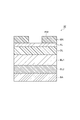
- FIG. 6A shows the state of the wafer W that is the process target of the process SAA (that is, the process target of the process shown in FIG. 5 described later).
- FIG. 6A is a cross-sectional view showing the state of the wafer W before the step (step SAA) shown in FIG.
- the wafer W shown in part (a) of FIG. 6 includes a layer to be processed J1 and a mask J2.
- the mask J2 is provided on the main surface J11 of the layer to be processed J1 (when the mask J2 corresponds to the mask MK, the main surface J11 corresponds to the main surface FW of the wafer W).
- step SA11 after performing step SAA, the layer to be processed J1 is etched using a mask that has been subjected to a groove width adjustment process.
- the processing target layer J1 is the organic film OL
- the mask J2 is formed from the antireflection film AL by the etching performed in the process SA11. It is a mask.
- step SA21 after execution of step SAA, the layer to be processed J1 is etched using a mask that has been subjected to a groove width adjustment process.
- step SA31 after execution of step SAA, the layer to be processed J1 is etched using a mask that has been subjected to a groove width adjustment process.
- the processing target layer J1 is the etching target layer EL2
- the mask J2 is subjected to etching and ashing performed in the processes SA31 and SA32. It is a mask formed from the etching layer EL1.
- step SA41 after execution of step SAA, the layer to be processed J1 is etched using a mask that has been subjected to groove width adjustment processing.
- FIG. 5 is a flowchart showing an example of a process (step SAA) that can be included in the method shown in FIG. 1 and that adjusts the groove width of the pattern before etching.
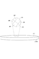
- FIG. 7 is a diagram schematically showing, as an example, a part of the plurality of regions ER of the main surface J11 of the processing target layer J1 of the wafer W divided in the method MT according to the embodiment.
- the plurality of regions ER do not overlap each other.
- the plurality of regions ER cover the main surface J11 (main surface FW of the wafer W) of the processing target layer J1.
- the shape of the region ER can be, for example, a region extending concentrically with respect to the central point of the main surface J11 of the processing target layer J1 (the central point of the main surface FW), or a lattice-shaped region. Not exclusively.
- the process SAA includes processes SB1 to SB7, and the processes SB5 to SB7 can be executed a plurality of times (repeatedly) according to the determination results of the processes SB3 and SB4.
- step SB1 the value of the groove width of the pattern of the mask J2 is measured for each of the plurality of regions ER of the main surface J11 of the processing target layer J1 by the optical observation apparatus OC of the processing system 1. .
- step SB2 (fourth step) subsequent to step SB1, a positive difference value obtained by subtracting the reference value of the groove width from the value of the groove width of the pattern of mask J2 measured in step SB1 is set in the target layer J1. Calculation is performed for each of the plurality of regions ER of the main surface J11.
- step SB3 subsequent to step SB2, whether or not the adjustment of the groove width of the pattern has already been performed once (if the adjustment of the groove width of the pattern has already been performed once, the adjustment of the groove width of the pattern will be described later in step SB5. (When it is already performed at least once in SB7), and the groove width of the pattern has not been adjusted yet (when the groove width of the pattern is adjusted first) (step SB3: No), the process proceeds to step SB5. If the groove width of the pattern has already been adjusted once in step SB3 (step SB3: Yes), the process proceeds to step SB4.
- step SB4 it is determined whether or not readjustment of the groove width of the pattern is necessary based on the difference value of the groove width of the pattern calculated in step SB2. If it is necessary to readjust the groove width of the pattern in step SB4 (step SB4: Yes), steps SB5 to SB7 are performed again. That is, when the steps SB1 and SB2 are re-executed after the execution of the steps SB5 to SB7, and the difference value calculated in the step SB2 by this re-execution does not satisfy the preset reference range (step SB4: Yes), Steps SB5 to SB7 are executed again.
- the reference range is a range including the reference value of the groove width used in step SB2.
- step SB4 if readjustment of the groove width of the pattern is not necessary (step SB4: No), that is, if the difference value calculated in step SB2 satisfies a preset reference range, step SAA Terminate the process.
- step SB3 Yes and step SB5 following step SB4: Yes, the wafer W is moved from the optical observation apparatus OC to the plasma processing apparatus 10 by the transfer robot Rb1 and the transfer robot Rb2, and the wafer W is moved to the plasma processing apparatus 10. Into the processing container 12.
- step SB6 (fifth step) subsequent to step SB5, the film thickness J3 of the difference value for each of the plurality of regions ER calculated in step SB2 (the film thickness for each of the plurality of regions ER is a plurality of regions in step SB2).
- a film having a difference value calculated for each ER) is formed on the surface J21 of the mask J2 of the wafer W carried into the processing container 12.
- the film J3 is a silicon oxide film.
- FIG. 6B is a cross-sectional view showing the state of the wafer W after the step (step SB6) shown in FIG. On the wafer W shown in FIG. 6B, a film J3 is formed on the surface J21 of the mask J2. The details of the processing performed in step SB6 will be described later.
- step SB7 following step SB6, the wafer W is moved from the plasma processing apparatus 10 to the optical observation apparatus OC by the transfer robot Rb1 and the transfer robot Rb2, and the wafer W is loaded into the optical observation apparatus OC.
- step SB1, step SB2, and step SB3 are performed again.
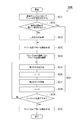
- FIG. 8 is a flowchart showing an example of a step of adjusting the groove width of the pattern, which is a part of the step shown in FIG. 5 (step SB6).
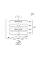
- FIG. 9 is a flowchart showing an example of a process (process SCC) that can be included in the process shown in FIG. 8 and that forms a uniform film on the main surface J11 of the layer to be processed J1.
- step SB6 includes steps SC1 to SC9.
- Steps SC5 to SC8 constitute a sequence SQ1.
- Sequence SQ1 and step SC9 are film formation processes for forming film J3 on surface J21 of mask J2 of wafer W.
- Steps SC1 to SC4 are preparatory processes necessary for executing the film forming process including the sequence SQ1 and the process SC9.
- step SC1 the wafer W carried into the processing container 12 of the plasma processing apparatus 10 is aligned and placed on the electrostatic chuck ESC.
- step SC2 subsequent to step SC1, as in step SB3, it is determined whether or not the adjustment of the pattern groove width has been performed once (if the adjustment of the pattern groove width has already been performed once, the pattern groove width If the adjustment of the pattern groove width has not been performed yet (the adjustment of the pattern groove width is performed first).
- Step SC2: No the process proceeds to step SC3.
- the determination result of step SC2 corresponds to the determination result of step SB3 shown in FIG.
- the process SC3 may not be executed when the process SAA including the process SC3 is performed in the process SA2 of etching the organic film (after the process SA1 and before the process SA21). .
- step SC2 if the adjustment of the groove width of the pattern has already been performed once (step SC2: Yes), the process proceeds to step SC4 or step SCC (the twelfth step). Since the determination result of step SC2 is the same as the determination result of step SB3, the determination process of step SC2 can be performed by referring to the determination result of step SB3.
- step SCC a film is formed conformally on the surface J21 of the mask J2 regardless of the plurality of regions ER. Details of the step SCC will be described later with reference to FIG.
- the process SB6 may have a configuration that does not include the process SCC. However, when the process SCC is included, between the process SC3 or the process SC2: No and the process SC4 (ie, the process SC4).
- the configuration may be such that the step SCC is performed before the SC4) or after the below-described step SC9: Yes (that is, after the film formation process).
- Step SC2 In step SC3 subsequent to Yes, the wafer W is irradiated with secondary electrons.
- step SC3 before execution of the sequence SQ1 for forming the film J3 on the surface J21 of the mask J2 and the step SC9, plasma is generated in the processing space Sp of the processing vessel 12 to apply a negative DC voltage to the upper electrode 30. This is a step of irradiating the mask J2 with secondary electrons.
- the mask J2 is formed before the film J3 is formed.
- the mask J2 can be prevented from being damaged by the subsequent process.
- process SC3 The processing content of process SC3 is demonstrated concretely.
- hydrogen gas and a rare gas are supplied into the processing container 12, and high-frequency power is supplied from the first high-frequency power source 62, thereby generating plasma in the processing space Sp.
- Hydrogen gas and a rare gas are supplied into the processing container 12 from a gas source selected from among a plurality of gas sources in the gas source group 40. Accordingly, positive ions in the processing space Sp are drawn into the upper electrode 30 and the positive ions collide with the upper electrode 30. When positive ions collide with the upper electrode 30, secondary electrons are emitted from the upper electrode 30. By irradiating the wafer W with the emitted secondary electrons, the mask J2 is modified.
- step SC3 when positive ions collide with the electrode plate 34, silicon that is a constituent material of the electrode plate 34 is released together with secondary electrons.
- the released silicon combines with oxygen released from the components of the plasma processing apparatus 10 exposed to the plasma.
- the oxygen is released from members such as the support portion 14, the insulating shielding member 32, and the deposition shield 46, for example.
- a silicon oxide compound is generated by the combination of silicon and oxygen, and the silicon oxide compound is deposited on the wafer W to cover and protect the mask J2.
- step SC3 of irradiating the mask J2 with secondary electrons plasma is generated in the processing space Sp and a negative DC voltage is applied to the upper electrode 30, thereby irradiating the mask J2 with secondary electrons.
- step SC4 the silicon oxide compound covers the mask J2
- damage to the mask J2 due to the subsequent process can be further suppressed.
- step SC3 for the purpose of reforming or forming a protective film by irradiation with secondary electrons, the bias power of the second high-frequency power supply 64 may be minimized to suppress silicon emission. It is also possible to exclude step SC3 in method MT.
- step SC4 (tenth step) through step SCC or without step SCC.
- step SC4 the temperature of the processing layer J1 of the wafer W is adjusted using the temperature adjusting unit HT for each of the plurality of regions ER of the main surface J11 of the processing layer J1 of the wafer W.
- step SC4 the correspondence between the temperature of the layer to be processed J1 and the film thickness of the film deposited on the surface J21 of the mask J2 on the layer to be processed J1 (film formed in the film forming process (sequence SQ1 and step SC9) described later).
- the temperature of the layer to be processed J1 is adjusted for each of the plurality of regions ER using the correspondence data DT acquired in advance and the film thickness corresponding to the difference value calculated for each of the plurality of regions ER in step SB2.
- Corresponding data DT is formed on the surface J21 of the mask J2 under the same conditions as the film forming process including the sequence SQ1 and the process SC9 (conditions excluding the temperature of the processed layer J1) for each temperature of the processed layer J1. This data is obtained in advance by depositing J3, and is stored in the storage unit of the control unit Cnt so as to be readable.
- the temperature for each of the plurality of regions ER in the processing target layer J1 of the wafer W carried into the processing container 12 is set for each of the plurality of regions ER in the process SB2.
- the temperature of the layer to be processed J1 is adjusted for each of the plurality of regions ER based on the correspondence data DT so that the temperature corresponds to the film thickness of the calculated difference value.
- step SC4 when step SB6 includes step SCC, that is, step SCC is performed before step SC4 and after step SC3 or after step SC2: No, or step SQ1 and step SC9.
- step SCC is performed before step SC4 and after step SC3 or after step SC2: No, or step SQ1 and step SC9.
- the temperature for each of the plurality of regions ER in the processing target layer J1 of the wafer W loaded into the processing container 12 is calculated for each of the plurality of regions ER in step SB2.
- the temperature of the layer to be processed J1 is set to the corresponding data DT for each of the plurality of regions ER so that the temperature corresponds to the value obtained by subtracting the film thickness of the film conformally formed in step SCC from the film thickness of the difference value. Adjust based on.
- a film (film J3,%) Is formed on the surface J21 of the mask J2 on the processing target layer J1 of the wafer W carried into the processing container 12.
- a part of the film J3 is formed when the process SCC is performed in the process SB6.
- the film formation process including the sequence SQ1 and the process SC9 is performed by applying a silicon oxide film on the surface J21 of the mask J2 of the wafer W with a uniform thickness for each of a plurality of regions ER by a method similar to the ALD (Atomic Layer Deposition) method. It is a process of forming formally.
- step SC5 of sequence SQ1 the temperature of the processing target layer J1 of the wafer W adjusted for each of the plurality of regions ER in step SC4 is maintained. For this reason, the film formed by the film formation process can have a different thickness for each of the plurality of regions ER.
- the groove width of the mask J2 is a desired value (the reference value of the groove width for each of the plurality of regions ER used for calculating the difference value in step SB2). It becomes.
- the sequence SQ1 includes processes SC5 to SC8.
- step SC5 (sixth step)
- the first gas G1 is supplied into the processing container 12.
- a first gas G1 containing silicon is introduced into the processing container 12.
- the first gas G1 includes an aminosilane-based gas that is organically contained.
- an aminosilane-based gas having a molecular structure with a relatively small number of amino groups can be used.
- monoaminosilane H 3 —Si—R (R contains organic).
- An optionally substituted amino group) can be used.
- the aminosilane-based gas used as the first gas G1 can include an aminosilane that can have 1 to 3 silicon atoms, or can include an aminosilane that has 1 to 3 amino groups. Can do.
- An aminosilane having 1 to 3 silicon atoms is a monosilane having 1 to 3 amino groups (monoaminosilane), a disilane having 1 to 3 amino groups, or a trisilane having 1 to 3 amino groups It can be.
- the above aminosilane can have an optionally substituted amino group.
- the amino group can be substituted with any of a methyl group, an ethyl group, a propyl group, and a butyl group.
- a first gas G1 of an aminosilane-based gas that is organically contained is supplied from the gas source selected from the plurality of gas sources of the gas source group 40 into the processing container 12. In step SC5, plasma of the first gas G1 is not generated.
- the processing time required in the process SC5 is within the time during which the film thickness of the film deposited on the surface J21 of the mask J2 on the processing layer J1 in the process SC5 increases or decreases depending on the temperature of the processing layer J1. .
- Such a processing time is a self-limited region in the ALD method (a processing time during which a film having a film thickness independent of the temperature of the layer to be processed J1 can be formed on the surface J21 of the mask J2 on the layer to be processed J1. It can be said that the processing time is shorter than the processing time.
- the molecules of the first gas G1 serve as a reaction precursor (layer Ly1) as a main surface J11 of the layer to be processed J1 (specifically, a mask J2 on the main surface J11). To the surface J21). The molecules of the first gas G1 adhere to the surface J21 of the mask J2 by chemical adsorption based on chemical bonds, and plasma is not used.
- the first gas G1 can be attached to the surface J21 of the mask J2 by chemical bonding under the temperature of the processing target layer J1 adjusted for each of the plurality of regions ER in step SC4, and contains silicon. If it does, it can be used.
- the reason for selecting monoaminosilane is that the monoaminosilane has a relatively high electronegativity and a molecular structure having polarity. This is because chemisorption can be performed relatively easily.
- the reaction precursor layer Ly1 formed by the molecules of the first gas G1 adhering to the surface J21 of the mask J2 is close to a monomolecular layer (single layer) because the adhesion is chemical adsorption. .
- the silicon reaction precursor (layer Ly1) is formed on the mask J2 along the atomic layer of the surface J21 of the mask J2 by the process SC5. Formed.
- step SC6 (seventh step) subsequent to step SC5, the inside of the processing container 12 is purged. Specifically, the first gas G1 supplied in step SC5 is exhausted.
- an inert gas such as a nitrogen gas or a rare gas (eg, Ar gas) may be supplied into the processing container 12 as a purge gas. That is, the purge in step SC6 may be either a gas purge for flowing an inert gas into the processing container 12 or a purge by evacuation.
- step SC6 molecules excessively attached on the surface J21 of the mask J2 can also be removed.
- the reaction precursor layer Ly1 is an extremely thin monomolecular layer.
- step SC7 (eighth step) subsequent to step SC6, as shown in part (b) of FIG. 10, plasma P1 of the second gas is generated in the processing space Sp of the processing vessel 12.
- the second gas includes a gas containing oxygen atoms and carbon atoms, and may include, for example, carbon dioxide gas.
- the temperature of the layer to be processed J1 of the wafer W when the second gas plasma P1 is generated may be, for example, not less than 0 degrees Celsius and not more than 200 degrees Celsius.
- a second gas containing a gas containing oxygen atoms and carbon atoms is supplied into the processing container 12 from a gas source selected from the plurality of gas sources of the gas source group 40. Then, high frequency power is supplied from the first high frequency power supply 62.
- the bias power of the second high-frequency power source 64 it is possible to apply the bias power of the second high-frequency power source 64, and it is also possible to generate plasma only by the second high-frequency power source 64.
- a high-frequency bias power is supplied from the second high-frequency power supply 64 and the exhaust device 50 is operated to set the pressure in the space in the processing container 12 to a preset pressure. In this way, the plasma P1 of the second gas is generated in the processing space Sp.
- a layer Ly2 (a layer included in the film J3) which is a silicon oxide film is formed as a monomolecular layer. Since the carbon radical can function to suppress oxygen erosion to the mask J2, the silicon oxide film can be stably formed on the surface J21 of the mask J2 as a protective film.
- the bond energy of the Si—O bond of the silicon oxide film is about 192 [kcal], and various bond types of the organic film forming the mask are a C—C bond, a C—H bond, and a C—F bond. Since it is higher than the respective binding energies (about 50-110 [kcal], about 70-110 [kcal], about 100-120 [kcal]), the silicon oxide film can function as a protective film.
- the oxygen atoms are oxidized on the mask J2 by being combined with the silicon reaction precursor (layer Ly1) provided on the mask J2.
- the layer Ly2 of the silicon film can be formed conformally with a different film thickness for each of the plurality of regions ER.
- the second gas contains carbon atoms, erosion of the mask J2 by oxygen atoms can be suppressed by the carbon atoms. Therefore, in the sequence SQ1, the silicon oxide film layer Ly2 is formed on the surface J21 of the mask J2 with a uniform film thickness according to the respective temperatures of the plurality of regions ER by a method similar to the ALD method. Each region ER can be formed conformally.
- step SC8 (9th step) subsequent to step SC7, the inside of the processing container 12 is purged. Specifically, the second gas supplied in step SC7 is exhausted.
- an inert gas such as nitrogen gas or a rare gas (eg, Ar) may be supplied into the processing container 12 as a purge gas.
- the purge in step SC8 may be either a gas purge for flowing an inert gas into the processing container 12 or a purge by evacuation.
- step SC9 following sequence SQ1, it is determined whether or not the number of repetitions of sequence SQ1 has reached a preset number (for example, 50 times), and when it is determined that the number has not been reached (step SC9). : No), sequence SQ1 is executed again, and when it is determined that the number of times has been reached (step SC9: Yes), step SB6 is terminated. That is, in step SC9, execution of the sequence SQ1 is repeated until the number of repetitions of the sequence SQ1 reaches a preset number of times, and the film corresponding to the temperature of each of the plurality of regions ER is applied to the surface J21 of the mask J2. A thick film is formed for each of the plurality of regions ER.
- a preset number for example, 50 times
- the number of repetitions of the sequence SQ1 controlled by the process SC9 is the same as the processing time in the process SC5 and the film formed by the film formation process consisting of the sequence SQ1 and the process SC9 (the film S3 is executed in the film J3 or the process SB6). In this case, it is determined according to the film thickness of a part of the film J3).
- the process SCC includes a sequence SQ2 and a process SD5.
- the sequence SQ2 includes steps SD1 to SD4.
- the process SD1 of the sequence SQ2 corresponds to the process SC5 of the sequence SQ1 shown in FIG. 8, but the temperature of the processing target layer J1 in the process SD1 is different from the temperature of the processing target layer J1 in the process SC5.
- the process SD1 is different from the process SC5 in that the process time required in the process SD1 is different from the process time required in the process SC5.
- steps SD2 to SD4 in sequence SQ2 the same processing is performed as in each of steps SC6 to SC8 in sequence SQ1 shown in FIG.
- the number of repetitions of the sequence SQ2 controlled by the process SD5 is determined according to the film thickness of the film (part of the film J3) formed by the process SCC.
- the film J3 formed in step SB6 includes a film formed in step SCC and a film formed in the film formation process (sequence SQ1 and step SC9).
- the film thickness of the film J3 formed in step SB6 is the total value of the film thickness of the film formed in step SCC and the film thickness formed in the film formation process (sequence SQ1 and step SC9).
- the processing time in the step SD1 of the sequence SQ2 is a self-limited region in the ALD method (a film thickness independent of the temperature of the layer to be processed J1 can be formed on the surface J21 of the mask J2 on the layer to be processed J1). Processing time), which is longer than the processing time in step SC5 of sequence SQ1.
- the temperature of the processing target layer J1 of the wafer W may be, for example, 0 degrees Celsius or more and 200 degrees Celsius or less.
- Correspondence data DT indicates the correspondence between the temperature of the layer to be processed J1 and the film thickness of the film deposited on the surface J21 of the mask J2 on the layer to be processed J1 (film formed by the film formation process (sequence SQ1 and step SC9)).
- the film J3 is formed on the surface J21 of the mask J2 under the same conditions (except for the temperature of the layer to be processed J1) as the film forming process including the sequence SQ1 and the step SC9 for each temperature of the layer to be processed J1. Is obtained in advance before the execution of the method MT.
- the processing time in the process SC5 (the value of the processing time is hereinafter referred to as TM) and the film formed by the film formation process
- VL the relationship with the film thickness
- F1 the relationship is hereinafter referred to as a function of the processing time (TM) and the temperature (KR)
- VL ⁇ 1 (KR) ⁇ ln (TM) + ⁇ 1 (KR ) (Equation 1).
- ⁇ 1 (KR) is a constant determined for each KR
- ln (TM) is a natural logarithm for TM
- ⁇ 1 (KR) is a constant determined for each KR.
- Equation 1 ⁇ 1 (KR) and ⁇ 1 (KR) included in Equation 1 can be approximated as follows.
- ⁇ 2 and ⁇ 2 are constants determined when calculating Equation 2 (approximate equation).
- ⁇ 3 and ⁇ 3 are constants determined when calculating Equation 3 (approximate equation).
- ln (KR) is the natural logarithm for KR.
- the step SAA of adjusting the groove width of the pattern of the mask J2 is performed before the step SA11 (or step SA21, step SA31, step SA41) of etching the layer to be processed J1.
- step SAA the main surface J11 of the layer to be processed J1 is divided into a plurality of regions ER.
- steps SB1 and SB2 the difference value between the groove width of the mask J2 and the reference value of the groove width is determined for each of the plurality of regions ER.
- a film J3 having a film thickness corresponding to the difference value is formed on the mask J2, and the groove width of the mask is corrected to the reference value for each of the plurality of regions ER.
- step SB6 a film is formed in high detail for each atomic layer on the mask J2 by a method similar to the ALD method using a film formation process in which steps SC5 to SC8 are repeatedly executed. Since the film thickness of the film formed by the film formation process varies depending on the temperature of the layer to be processed J1, in step SC4, correspondence data DT indicating the correspondence between the temperature of the layer to be processed J1 and the film thickness of the film to be formed is obtained. The temperature of the layer to be processed J1 is adjusted so as to be a temperature necessary for forming a film having a film thickness corresponding to the difference value calculated in the step SB2 for each of the plurality of regions ER.
- the correction amount of the groove of the mask J2 corresponds to each of the plurality of regions ER of the main surface J11 of the layer to be processed J1.
- the film thickness is determined, the temperature of the layer to be processed J1 necessary for forming the film thickness is determined using the correspondence data DT, and the temperature of the layer to be processed J1 is adjusted at the temperature determined for each of the plurality of regions ER.
- the film formation process similar to the ALD method is performed, the variation in the pattern of the mask J2 can be suppressed in detail and sufficiently for each of the plurality of regions ER of the main surface J11 of the layer to be processed J1.
- step SC4 the film can be partially formed by the step SCC without adjusting the temperature of the layer to be processed J1 performed for each of the plurality of regions ER in step SC4.
- the difference value of the groove width of the mask J2 is calculated again to determine whether or not the difference value is within the reference range (steps SB1 to SB4). If it is not within the reference range, the film J3 is formed again, so that the variation in the groove width of the mask J2 can be further sufficiently suppressed.
- Refrigerant flow path 26a Pipe, 26b Pipe, 28 Gas supply line, 30 Upper electrode, 32 Insulating shielding member, 34 Electrode plate, 34a Gas discharge hole, 36 Electrode support, 36a Gas diffusion chamber, 36b Gas flow hole, 36c ... Gas inlet, 38 ... Gas supply pipe, 40 ... Gas source group, 42 ... Valve group, 44 ... Flow rate controller group, 46 ... Depot shield, 48 ... Gas plate, 50 ... exhaust device, 52 ... exhaust pipe, 54 ... gate valve, 62 ... first high frequency power source, 64 ... second high frequency power source, 66 ... matching device, 68 ... matching device, 70 ... power source, AL ... Antireflection film, Cnt ... control unit, DT ...
Landscapes
- Chemical & Material Sciences (AREA)
- Engineering & Computer Science (AREA)
- Materials Engineering (AREA)
- Organic Chemistry (AREA)
- Drying Of Semiconductors (AREA)
- Physics & Mathematics (AREA)
- Plasma & Fusion (AREA)
- Formation Of Insulating Films (AREA)
- Electrical Discharge Machining, Electrochemical Machining, And Combined Machining (AREA)
- Testing Of Coins (AREA)
Abstract
一実施形態の方法MTでは、処理対象のウエハWの被処理層J1のエッチングの前に、被処理層J1の主面J11を複数の領域ERに区分けしたうえで、工程SB2で被処理層J1上に設けられたマスクJ2の溝幅と当該溝幅の基準値との差分値を複数の領域ERごとに算出し、工程SB6で、被処理層J1の温度と形成する膜の膜厚との対応を示す対応データDTを用いて複数の領域ERごとに差分値に対応する膜厚の膜の形成に必要な温度となるように被処理層J1の温度を調節したうえで、ALD法と同様の膜形成処理を用いてマスクJ2に膜を原子層ごとに形成して、差分値に対応する膜厚の膜J3をマスクJ2に形成して複数の領域ERごとに溝幅を基準値に補正する。
Description
本発明の実施形態は、被処理体を処理する方法に関するものである。
半導体デバイスといった電子デバイスの製造プロセスでは、被処理層上にマスクを形成し、当該マスクのパターンを当該被処理層に転写するためにエッチングが行われる。マスクとしては、一般的に、レジストマスクが用いられる。レジストマスクは、フォトリソグラフィ技術によって形成される。従って、被エッチング層に形成されるパターンの限界寸法は、フォトリソグラフィ技術によって形成されるレジストマスクの解像限界や、パターン密度等によって影響を受けるが、近年では、電子デバイスの高集積化に伴い、レジストマスクの解像限界よりも小さい寸法のパターンを形成することが要求されるようになっている。このため、特許文献1に記載されているように、レジストマスク上にシリコン酸化膜を形成することによって、当該レジストマスクの寸法を調整し、当該レジストマスクによって提供される開口の幅を縮小する技術が提案されている。
特許文献1に開示されている微細パターン形成方法では、微細パターンを形成しようとする物質膜上にフォトレジストパターンを形成し、その上にシリコン酸化膜を蒸着するが、下部のフォトレジストパターンに損傷を加えずにコンフォーマルに薄く形成しなければならない。さらにこの後に、下部膜に対してドライエッチングを実施するが、初期にはフォトレジストパターンの側壁にスペーサを形成し、次にフォトレジストパターン上にポリマー膜を形成する。
レジストマスクの解像限界よりも小さな寸法をもったパターンを形成する場合、パターンの溝の高詳細な最小線幅(CD:Critical Dimension)の制御が要求される。パターンが詳細であるほど、最小線幅のバラつきの影響が大きくなる。従って、被処理体上のパターン形成においては、高集積化に伴う微細化のために、高精度の最小線幅のバラつきを抑制する方法の実現が必要となる。
一態様においては、被処理体を処理する方法が提供される。被処理体は、被処理層と被処理層の主面に設けられたマスクとを備える。この方法は、マスクのパターンの溝幅を調節する第1の工程と、第1の工程の実行後に、マスクを用いて被処理層をエッチングする第2の工程と、を備える。主面は、当該方法において複数の領域に区分けされており、第1の工程は、溝幅の値を当該方法において区分けされた複数の領域ごとに測定する第3の工程と、第3の工程の実行後に、第3の工程で測定された溝幅の値から溝幅の基準値を差し引いた正の差分値を、複数の領域ごとに算出する第4の工程と、第4の工程の実行後に、第4の工程で算出された複数の領域ごとの差分値の膜厚の膜を、プラズマ処理装置の処理容器内に搬入された被処理体のマスクの表面に形成する第5の工程と、を備える。第5の工程は、処理容器内に第1のガスを供給する第6の工程と、第6の工程の実行後に、処理容器内をパージする第7の工程と、第7の工程の実行後に、処理容器内で第2のガスのプラズマを生成する第8の工程と、第8の工程の実行後に、処理容器内をパージする第9の工程と、を含むシーケンスを繰り返し実行する膜形成処理において被処理層の温度と被処理層上のマスクの表面に堆積する膜の膜厚との対応を示す予め取得された対応データと、第4の工程において複数の領域ごとに算出された差分値に対応する膜厚とを用いて、複数の領域ごとに、処理容器内に搬入された被処理体の被処理層の温度を調節する第10の工程と、第10の工程の実行後に、膜形成処理を実行して、被処理層上のマスクの表面に膜を形成する第11の工程と、を備える。第6の工程で要する処理時間は、第6の工程において被処理層上のマスクの表面に堆積する膜の膜厚が被処理層の温度の高低に応じて増減する状態となる時間内にあり、第1のガスは、アミノシラン系ガスを含み、第2のガスは、酸素原子および炭素原子を含有するガスを含むことができる。
上記方法では、被処理層をエッチングする第2の工程の前に、マスクのパターンの溝幅を調節する第1の工程を実施する。第1の工程では、被処理層の主面を複数の領域に区分けし、第3の工程および第4の工程ではマスクの溝幅と当該溝幅の基準値との差分値を複数の領域ごとに算出し、第5の工程では当該差分値に対応する膜厚の膜をマスクに形成して複数の領域ごとにマスクの溝幅を当該基準値に補正する。第5の工程では、第6の工程~第9の工程を繰り返し実行する膜形成処理を用いてALD(Atomic Layer Deposition)法と同様の方法によってマスクに膜を原子層ごとに高詳細に形成する。膜形成処理で形成される膜の膜厚は被処理層の温度に応じて異なるので、第10の工程では、被処理層の温度と形成する膜の膜厚との対応を示す対応データを用いて、複数の領域ごとに、第4の工程で算出した差分値に対応する膜厚の膜の形成に必要な温度となるように、被処理層の温度を調節する。このように、第2の工程で行うエッチングの前に、被処理層の主面の複数の領域ごとに、マスクの溝の補正量に対応する膜厚が決定され、当該膜厚の形成に必要な被処理層の温度が対応データを用いて決定され、複数の領域ごとに決定された温度で被処理層の温度が調節された状態で、ALD法と同様の膜形成処理が行われるので、マスクのパターンのバラつきが被処理層の主面の複数の領域ごとに詳細且つ十分に抑制され得る。
一実施形態では、第10の工程は、処理容器内に搬入された被処理体の被処理層における複数の領域ごとの温度が、第4の工程において複数の領域ごとに算出された差分値の膜厚に対応する温度となるように、複数の領域ごとに被処理層の温度を、対応データに基づいて調節する。
一実施形態では、第5の工程は、複数の領域によらずにマスクの表面に対しコンフォーマルに膜を形成する第12の工程を備え、第10の工程は、処理容器内に搬入された被処理体の被処理層における複数の領域ごとの温度が、第4の工程において複数の領域ごとに算出された差分値の膜厚から第12の工程でコンフォーマルに形成される膜の膜厚を差し引いた値に対応する温度となるように、複数の領域ごとに被処理層の温度を対応データに基づいて調節し、第12の工程は、第10の工程の前または膜形成処理の後に行われる。このように、複数の領域ごとの膜厚のうち共通の膜厚については、複数の領域ごとに行う被処理層の温度の調節を経ずに、部分的に膜の形成が可能となる。
一実施形態では、第1の工程は、第5の工程の実行後に第3の工程および第4の工程を再実行し、この再実行によって第4の工程で算出された差分値が予め設定された基準範囲を満たさない場合に、第5の工程を再実行する。このように、第5の工程によって膜の形成を行った後に、マスクの溝幅の差分値を再度算出して差分値が基準範囲にあるか否かを判定し、差分値が基準範囲にない場合には、膜の形成を再度行うので、マスクの溝幅のバラつきがさらに十分に抑制され得る。
一実施形態では、第1のガスのアミノシラン系ガスは、1~3個のケイ素原子を有するアミノシランを含み得る。第1のガスのアミノシラン系ガスは、1~3個のアミノ基を有するアミノシランを含み得る。このように第1のガスのアミノシラン系ガスには、1~3個のケイ素原子を含むアミノシランを用いることができる。また、第1のガスのアミノシラン系ガスには、1~3個のアミノ基を含むアミノシランを用いることができる。
以上説明したように、被処理体上のパターン形成において、高精度の最小線幅のバラつきを抑制する方法が提供される。
以下、図面を参照して種々の実施形態について詳細に説明する。なお、各図面において同一または相当の部分に対しては同一の符号を附すこととする。
図1は、一実施形態に係る被処理体を処理する方法を示す流図である。図1に示す方法MTは、被処理体を処理する方法の一実施形態である。図2は、図1に示す方法MTの適用対象である被処理体(以下、ウエハWという)を例示する断面図である。図2に示すウエハWは、基板BA、被エッチング層EL2、被エッチング層EL1、有機膜OL、反射防止膜AL、および、マスクMKを有している。
被エッチング層EL2は、基板BA上に設けられている。被エッチング層EL1は、被エッチング層EL2上に設けられている。被エッチング層EL1および被エッチング層EL2は、シリコンを含有する層であり、例えば、アモルファスシリコン層または多結晶シリコン層である。有機膜OLは、有機材料から構成された膜であり、被エッチング層EL1上に設けられている。反射防止膜ALは、Si含有反射防止膜であり、有機膜OL上に設けられている。マスクMKは、反射防止膜AL上であって、ウエハWの主面FWに設けられている。マスクMKは、有機材料から構成されたマスクであり、例えば、レジストマスクである。マスクMKには、開口を提供するパターンがフォトリソグラフィによって形成されている。
方法MT(被処理体を処理する方法)は、プラズマ処理装置を有する処理システムによって実行される。図3は、図1に示す方法MTの実施に用いることが可能な処理システムの一例を示す図である。図3に示す処理システム1は、制御部Cnt、台122a、台122b、台122c、台122d、収容容器124a、収容容器124b、収容容器124c、収容容器124d、ローダモジュールLM、ロードロックチャンバLL1、ロードロックチャンバLL2、トランスファーチャンバ121、プラズマ処理装置10を備えている。
制御部Cntは、プロセッサ、記憶部、入力装置、表示装置等を備えるコンピュータであり、処理システム1の後述する各部を制御する。制御部Cntは、搬送ロボットRb1、搬送ロボットRb2、光学観察装置OC、プラズマ処理装置10等に接続されており、更に、後述する図4に示すプラズマ処理装置10においては、バルブ群42、流量制御器群44、排気装置50、第1の高周波電源62、整合器66、第2の高周波電源64、整合器68、電源70、ヒータ電源HP、チラーユニット等に接続されている。
制御部Cntは、方法MTの各工程において処理システム1の各部を制御するためのコンピュータプログラム(入力されたレシピに基づくプログラム)に従って動作し、制御信号を送出する。制御部Cntからの制御信号により、処理システム1の各部、例えば、搬送ロボットRb1,Rb2、光学観察装置OC、および、プラズマ処理装置10の各部を制御する。図4に示すプラズマ処理装置10においては、制御部Cntからの制御信号により、ガスソース群40から供給されるガスの選択および流量、排気装置50の排気、第1の高周波電源62および第2の高周波電源64からの電力供給、電源70からの電圧印加、ヒータ電源HPの電力供給、チラーユニットからの冷媒流量および冷媒温度を制御することが可能である。なお、本明細書において開示される被処理体を処理する方法MTの各工程は、制御部Cntによる制御によって処理システム1の各部を動作させることによって実行され得る。制御部Cntの記憶部には、方法MTを実行するためのコンピュータプログラム、および、方法MTの実行に用いられる各種のデータ(例えば、後述する対応データDT)が、読出し自在に格納されている。
台122a~122dは、ローダモジュールLMの一縁に沿って配列されている。台122a~122dのそれぞれの上には、収容容器124a~124dがそれぞれ設けられている。収容容器124a~124d内には、ウエハWが収容され得る。
ローダモジュールLM内には、搬送ロボットRb1が設けられている。搬送ロボットRb1は、収容容器124a~124dの何れかに収容されているウエハWを取り出して、ウエハWを、ロードロックチャンバLL1またはLL2に搬送する。
ロードロックチャンバLL1およびLL2は、ローダモジュールLMの別の一縁に沿って設けられており、ローダモジュールLMに接続されている。ロードロックチャンバLL1およびLL2は、予備減圧室を構成している。ロードロックチャンバLL1およびLL2は、トランスファーチャンバ121にそれぞれ接続されている。
トランスファーチャンバ121は、減圧可能なチャンバであり、トランスファーチャンバ121内には搬送ロボットRb2が設けられている。トランスファーチャンバ121には、プラズマ処理装置10が接続されている。搬送ロボットRb2は、ロードロックチャンバLL1またはロードロックチャンバLL2からウエハWを取り出して、当該ウエハWをプラズマ処理装置10に搬送する。
処理システム1は、光学観察装置OCを備える。ウエハWは、搬送ロボットRb1および搬送ロボットRb2によって、光学観察装置OCとプラズマ処理装置10との間で移動され得る。搬送ロボットRb1によってウエハWが光学観察装置OC内に収容され、光学観察装置OC内においてウエハWの位置合わせが行われた後に、光学観察装置OCは、ウエハWのマスク(例えばマスクMK等)のパターンの溝幅を測定し、測定結果を制御部Cntに送信する。光学観察装置OCでは、主面FWの複数の領域ER(後述)ごとに、マスクのパターンの溝幅が測定され得る。
図4は、図3に示す処理システムが備えることが可能なプラズマ処理装置の一例を示す図である。図4には、被処理体を処理する方法MTの種々の実施形態で利用可能なプラズマ処理装置10の断面構造が概略的に示されている。
図4に示すように、プラズマ処理装置10は、平行平板の電極を備えるプラズマエッチング装置であり、処理容器12を備えている。処理容器12は、略円筒形状を有しており、処理空間Spを画定する。処理容器12は、例えば、アルミニウムから構成されており、その内壁面には陽極酸化処理が施されている。処理容器12は保安接地されている。
処理容器12の底部上には、略円筒状の支持部14が設けられている。支持部14は、例えば、絶縁材料から構成されている。支持部14を構成する絶縁材料は、石英のように酸素を含み得る。支持部14は、処理容器12内において、処理容器12の底部から鉛直方向に延在している。処理容器12内には、載置台PDが設けられている。載置台PDは、支持部14によって支持されている。
載置台PDは、載置台PDの上面においてウエハWを保持する。ウエハWの主面FWは、載置台PDの上面に接触するウエハWの裏面の反対側にあり、上部電極30に向いている。載置台PDは、下部電極LEおよび静電チャックESCを有している。下部電極LEは、第1プレート18aおよび第2プレート18bを含んでいる。第1プレート18aおよび第2プレート18bは、例えばアルミニウムといった金属から構成されており、略円盤形状をなしている。第2プレート18bは、第1プレート18a上に設けられており、第1プレート18aに電気的に接続されている。
第2プレート18b上には、静電チャックESCが設けられている。静電チャックESCは、導電膜である電極を、一対の絶縁層の間または一対の絶縁シートの間に配置した構造を有している。静電チャックESCの電極には、直流電源22がスイッチ23を介して電気的に接続されている。ウエハWは、載置台PDに載置されている場合に、静電チャックESCに接する。ウエハWの裏面(主面FWの反対側の面)は、静電チャックESCに接する。静電チャックESCは、直流電源22からの直流電圧により生じるクーロン力等の静電力によりウエハWを吸着する。これにより、静電チャックESCは、ウエハWを保持することができる。
第2プレート18bの周縁部上には、ウエハWのエッジおよび静電チャックESCを囲むようにフォーカスリングFRが配置されている。フォーカスリングFRは、エッチングの均一性を向上させるために設けられている。フォーカスリングFRは、エッチング対象の膜の材料によって適宜選択される材料から構成されており、例えば、石英から構成され得る。
第2プレート18bの内部には、冷媒流路24が設けられている。冷媒流路24は、温調機構を構成している。冷媒流路24には、処理容器12の外部に設けられたチラーユニット(図示略)から配管26aを介して冷媒が供給される。冷媒流路24に供給される冷媒は、配管26bを介してチラーユニットに戻される。このように、冷媒流路24には、冷媒が循環するように供給される。この冷媒の温度を制御することによって、静電チャックESCによって支持されたウエハWの温度が制御され得る。
プラズマ処理装置10には、ガス供給ライン28が設けられている。ガス供給ライン28は、伝熱ガス供給機構からの伝熱ガス、例えばHeガスを、静電チャックESCの上面とウエハWの裏面との間に供給する。
プラズマ処理装置10には、ウエハWの温度を調節する温度調節部HTが設けられている。温度調節部HTは、静電チャックESCに内蔵されている。温度調節部HTには、ヒータ電源HPが接続されている。ヒータ電源HPから温度調節部HTに電力が供給されることにより、静電チャックESCの温度が調整され、静電チャックESC上に載置されるウエハWの温度が調整されるようになっている。なお、温度調節部HTは、第2プレート18b内に埋め込まれていることもできる。
温度調節部HTは、熱を発する複数の加熱素子と、当該複数の加熱素子のそれぞれの周囲の温度をそれぞれ検出する複数の温度センサとを備える。複数の加熱素子のそれぞれは、ウエハWが静電チャックESC上に位置合わせされて載置されている場合に、ウエハWの主面FWの複数の領域ER(後述)ごとに、設けられている。制御部Cntは、ウエハWが静電チャックESC上に位置合わせされて載置されている場合に、ウエハWの主面FWの複数の領域ERのそれぞれに対応する加熱素子および温度センサを領域ERと関連付けて認識する。制御部Cntは、領域ERと、この領域ERに対応する加熱素子および温度センサとを、複数の領域ごと(複数の領域ERごと)に、例えば数字や文字等の番号等によって、識別し得る。制御部Cntは、一の領域ERの温度を、当該一の領域ERに対応する箇所に設けられた温度センサによって検出し、当該一の領域ERに対する温度調節を、当該一の領域ERに対応する箇所に設けられた加熱素子によって行う。なお、ウエハWが静電チャックESC上に載置されている場合に一の温度センサによって検出される温度は、ウエハWのうち当該温度センサ上の領域ERの温度(より具体的には、後述の被処理層J1における領域ERの温度)と同様である。
プラズマ処理装置10は、上部電極30を備えている。上部電極30は、載置台PDの上方において、載置台PDと対向配置されている。下部電極LEと上部電極30とは、互いに略平行に設けられており、平行平板電極を構成する。上部電極30と下部電極LEとの間には、ウエハWにプラズマ処理を行うための処理空間Spが提供されている。
上部電極30は、絶縁性遮蔽部材32を介して、処理容器12の上部に支持されている。絶縁性遮蔽部材32は、絶縁材料から構成されており、例えば、石英のように酸素を含み得る。上部電極30は、電極板34および電極支持体36を含み得る。電極板34は処理空間Spに面しており、電極板34には複数のガス吐出孔34aが設けられている。電極板34は、一実施形態では、シリコンを含有する。別の実施形態では、電極板34は、酸化シリコンを含有し得る。
電極支持体36は、電極板34を着脱自在に支持するものであり、例えばアルミニウムといった導電性材料から構成され得る。電極支持体36は、水冷構造を有し得る。電極支持体36の内部には、ガス拡散室36aが設けられている。ガス拡散室36aからは、ガス吐出孔34aに連通する複数のガス通流孔36bが下方に延びている。電極支持体36には、ガス拡散室36aに処理ガスを導くガス導入口36cが形成されており、ガス導入口36cには、ガス供給管38が接続されている。
ガス供給管38には、バルブ群42および流量制御器群44を介して、ガスソース群40が接続されている。ガスソース群40は、複数のガスソースを有している。複数のガスソースは、有機含有されたアミノシラン系ガスのソース、フルオロカーボン系ガス(CxFyガス(x、yは1~10の整数))のソース、酸素原子および炭素原子を有するガス(例えば二酸化炭素ガス等)のソース、窒素ガスのソース、水素ガスのソース、および、希ガスのソースを含み得る。アミノシラン系ガスとして、アミノ基の数が比較的に少ない分子構造のものが用いられることができ、例えば、モノアミノシラン(H3-Si-R(Rは有機を含んでおり置換されていても良いアミノ基))が用いられ得る。上記のアミノシラン系ガス(後述の第1のガスG1に含まれるガス)は、1~3個のケイ素原子を有し得るアミノシランを含むことができ、または、1~3個のアミノ基を有するアミノシランを含むことができる。1~3個のケイ素原子を有するアミノシランは、1~3個のアミノ基を有するモノシラン(モノアミノシラン)、1~3個のアミノ基を有するジシラン、または、1~3個のアミノ基を有するトリシランであり得る。さらに、上記のアミノシランは、置換されていてもよいアミノ基を有し得る。さらに、上記のアミノ基は、メチル基、エチル基、プロピル基、および、ブチル基の何れかによって置換され得る。さらに、上記のメチル基、エチル基、プロピル基、または、ブチル基は、ハロゲンによって置換され得る。フルオロカーボン系ガスとしては、CF4ガス、C4F6ガス、C4F8ガスといった任意のフルオロカーボン系ガスが用いられ得る。希ガスとしては、Arガス、Heガスといった任意の希ガスが用いられ得る。
バルブ群42は複数のバルブを含んでおり、流量制御器群44はマスフローコントローラといった複数の流量制御器を含んでいる。ガスソース群40の複数のガスソースのそれぞれは、バルブ群42の対応のバルブおよび流量制御器群44の対応の流量制御器を介して、ガス供給管38に接続されている。したがって、プラズマ処理装置10は、ガスソース群40の複数のガスソースのうち選択された一以上のガスソースからのガスを、個別に調整された流量で、処理容器12内に供給することが可能である。
プラズマ処理装置10では、処理容器12の内壁に沿ってデポシールド46が着脱自在に設けられている。デポシールド46は、支持部14の外周にも設けられている。デポシールド46は、処理容器12にエッチング副生物(デポ)が付着することを防止するものであり、アルミニウム材にY2O3等のセラミックスを被覆することにより構成され得る。デポシールドは、Y2O3の他に、例えば、石英のように酸素を含む材料から構成され得る。
処理容器12の底部側、且つ、支持部14と処理容器12の側壁との間には排気プレート48が設けられている。排気プレート48は、例えば、アルミニウム材にY2O3等のセラミックスを被覆することにより構成され得る。排気プレート48の下方、且つ、処理容器12には、排気口12eが設けられている。排気口12eには、排気管52を介して排気装置50が接続されている。排気装置50は、ターボ分子ポンプなどの真空ポンプを有しており、処理容器12内の空間を所望の真空度まで減圧することができる。処理容器12の側壁にはウエハWの搬入出口12gが設けられており、搬入出口12gはゲートバルブ54により開閉可能となっている。
プラズマ処理装置10は、第1の高周波電源62および第2の高周波電源64を更に備えている。第1の高周波電源62は、プラズマ生成用の第1の高周波電力を発生する電源であり、27~100[MHz]の周波数、一例においては60[MHz]の高周波電力を発生する。また、第1の高周波電源62は、パルス仕様を備えており、周波数5~10[kHz]、Duty50~100%で制御可能である。第1の高周波電源62は、整合器66を介して上部電極30に接続されている。整合器66は、第1の高周波電源62の出力インピーダンスと負荷側(下部電極LE側)の入力インピーダンスを整合させるための回路である。なお、第1の高周波電源62は、整合器66を介して下部電極LEに接続されていてもよい。
第2の高周波電源64は、ウエハWにイオンを引き込むための第2の高周波電力、すなわち高周波バイアス電力を発生する電源であり、400[kHz]~40.68[MHz]の範囲内の周波数、一例においては13.56[MHz]の周波数の高周波バイアス電力を発生する。また、第2の高周波電源64は、パルス仕様を備えており、周波数5~40[kHz]、Duty20~100%で制御可能である。第2の高周波電源64は、整合器68を介して下部電極LEに接続されている。整合器68は、第2の高周波電源64の出力インピーダンスと負荷側(下部電極LE側)の入力インピーダンスを整合させるための回路である。
プラズマ処理装置10は、電源70を更に備えている。電源70は、上部電極30に接続されている。電源70は、処理空間Sp内に存在する正イオンを電極板34に引き込むための電圧を、上部電極30に印加する。一例においては、電源70は、負の直流電圧を発生する直流電源である。このような電圧が電源70から上部電極30に印加されると、処理空間Spに存在する正イオンが、電極板34に衝突する。これにより、電極板34から二次電子および/またはシリコンが放出される。
以下、図1、図5、図8、図9を参照し、プラズマ処理装置10を備える処理システム1において実施される形態を例にとって、方法MTについて詳細に説明する。なお、方法MTは、処理システム1とは異なる処理システムにおいて実施されることも可能であり、そのような処理システムは、プラズマ処理装置10以外のプラズマ処理装置を備えることが可能である。
まず、図1に示す方法MTは、工程SA1~SA4を備える。工程SA1は、図2に示すマスクMKを用いて反射防止膜ALをエッチングする工程SA11(第2の工程)を備える。工程SA1に引き続く工程SA2は、工程SA11において行われるエッチングによって反射防止膜ALから形成されるマスクを用いて有機膜OLをエッチングする工程SA21(第2の工程)を備える。工程SA2に引き続く工程SA3は、工程SA21において行われるエッチングによって有機膜OLから形成されるマスクを用いて被エッチング層EL1をエッチングする工程SA31と、工程SA31の後に、有機膜OLから形成されるマスクをアッシングして除去する工程SA32とを備える。工程SA3に引き続く工程SA4は、工程SA31において行われるエッチングによって被エッチング層EL1から形成されるマスクを用いて被エッチング層EL2をエッチングする工程SA41を備える。
工程SA11では、反射防止膜ALをエッチングする。具体的には、ガスソース群40の複数のガスソースのうち選択したガスソースから、フルオロカーボンガスを含む処理ガスを処理容器12内に供給する。そして、第1の高周波電源62から高周波電力を供給する。第2の高周波電源64から高周波バイアス電力を供給する。排気装置50を動作させることによって、処理容器12内の圧力を所定の圧力に設定する。以上のようにして、フルオロカーボンガスのプラズマが処理容器12の処理空間Sp内で生成される。生成されたプラズマ中のフッ素を含む活性種は、反射防止膜ALの全領域のうちマスクMKから露出した領域をエッチングする。この反射防止膜ALのエッチングによって、有機膜OLに対するエッチングに用いられるマスクが反射防止膜ALから形成される。
工程SA21では、有機膜OLをエッチングする。具体的には、ガスソース群40の複数のガスソースのうち選択したガスソースから、窒素ガスと水素ガスとを含む処理ガスを処理容器12内に供給する。そして、第1の高周波電源62から高周波電力を供給する。第2の高周波電源64から高周波バイアス電力を供給する。排気装置50を動作させることによって、処理容器12内の圧力を所定の圧力に設定する。以上のようにして、窒素ガスと水素ガスとを含む処理ガスのプラズマが処理容器12の処理空間Sp内で生成される。生成されたプラズマ中の水素の活性種である水素ラジカルは、有機膜OLの全領域のうち、工程SA11で反射防止膜ALから形成されたマスクから露出した領域をエッチングする。この有機膜OLのエッチングによって、被エッチング層EL1に対するエッチングに用いられるマスクが有機膜OLから形成される。なお、有機膜OLをエッチングするガスとしては、酸素を含む処理ガスを用いてもよい。
工程SA2に引き続く工程SA3の工程SA31では、被エッチング層EL1をエッチングする。具体的には、ガスソース群40の複数のガスソースのうち選択したガスソースから、処理ガスを処理容器12内に供給する。処理ガスは、被エッチング層EL1を構成する材料に応じて適宜選択され得る。例えば、被エッチング層EL1が酸化シリコンから構成されている場合には、処理ガスは、フルオロカーボンガスを含み得る。そして、第1の高周波電源62から高周波電力を供給する。第2の高周波電源64から高周波バイアス電力を供給する。排気装置50を動作させることによって、処理容器12内の圧力を所定の圧力に設定する。これによって、プラズマが生成される。生成されたプラズマ中の活性種は、被エッチング層EL1の全領域のうち、工程SA21において行われたエッチングによって有機膜OLから形成されたマスクから露出した領域をエッチングする。工程SA31の後に、工程SA32では、有機膜OLから工程SA21で形成されたマスクをアッシングする。具体的には、ガスソース群40の複数のガスソースのうち選択したガスソースから、処理ガスを処理容器12内に供給する。処理ガスは、酸素ガス及び酸素原子を含み得る。そして、第1の高周波電源62から高周波電力を供給する。第2の高周波電源64から高周波バイアス電力を供給する。排気装置50を動作させることによって、処理容器12内の圧力を所定の圧力に設定する。これによって、プラズマが生成される。生成されたプラズマ中の活性種は、有機膜OLから工程SA21で形成されたマスクをアッシングする。なお、有機膜OLから工程SA21で形成されたマスクをアッシングするガスとしては、窒素ガスと水素ガスとを含む処理ガスが用いられ得る。
工程SA3に引き続く工程SA4の工程SA41では、被エッチング層EL2をエッチングする。具体的には、ガスソース群40の複数のガスソースのうち選択したガスソースから、処理ガスを処理容器12内に供給する。処理ガスは、被エッチング層EL2を構成する材料に応じて適宜選択され得る。例えば、被エッチング層EL2がアモルファスシリコンから構成されている場合には、処理ガスは、ハロゲン系のガスを含み得る。そして、第1の高周波電源62から高周波電力を供給する。第2の高周波電源64から高周波バイアス電力を供給する。排気装置50を動作させることによって、処理容器12内の圧力を所定の圧力に設定する。これによって、プラズマが生成される。生成されたプラズマ中の活性種は、被エッチング層EL2の全領域のうち、工程SA31,SA32において行われたエッチングおよびアッシングによって被エッチング層EL1から形成されたマスクから露出した領域をエッチングする。
工程SA1、工程SA2、工程SA3、および工程SA4は、エッチング前のパターンの溝幅の調節処理を行う工程SAA(第1の工程)を備え得る。工程SAAでは、エッチング前において、エッチングで用いるマスクのパターンの溝幅を調節する。工程SAAは、工程SA1で行われる場合には工程SA11の前に行われる。工程SAAは、工程SA2で行われる場合には工程SA21の前に行われる。工程SAAは、工程SA3で行われる場合には工程SA31の前に行われる。工程SAAは、工程SA4で行われる場合には工程SA41の前に行われる。
工程SAAの処理対象(すなわち、後述の図5に示す工程の処理対象)であるウエハWの状態を、図6の(a)部に示す。図6の(a)部は、図5に示す工程(工程SAA)の実施前のウエハWの状態を示す断面図である。図6の(a)部に示すウエハWは、被処理層J1と、マスクJ2とを備える。マスクJ2は、被処理層J1の主面J11(マスクJ2がマスクMKに対応する場合には、主面J11はウエハWの主面FWに対応する)に設けられる。
図1に示す工程SAAが反射防止膜ALをエッチングする工程SA1で実行される場合、被処理層J1は反射防止膜ALであり、マスクJ2はマスクMKである。工程SA11は、工程SAAの実行後に、溝幅の調節処理が行われたマスクを用いて被処理層J1をエッチングする。
図1に示す工程SAAが有機膜OLをエッチングする工程SA2で実行される場合、被処理層J1は有機膜OLであり、マスクJ2は工程SA11において行われるエッチングによって反射防止膜ALから形成されるマスクである。工程SA21は、工程SAAの実行後に、溝幅の調節処理が行われたマスクを用いて被処理層J1をエッチングする。
図1に示す工程SAAが被エッチング層EL1をエッチングする工程SA3で実行される場合、被処理層J1は被エッチング層EL1であり、マスクJ2は工程SA21において行われるエッチングによって有機膜OLから形成されるマスクである。工程SA31は、工程SAAの実行後に、溝幅の調節処理が行われたマスクを用いて被処理層J1をエッチングする。
図1に示す工程SAAが被エッチング層EL2をエッチングする工程SA4で実行される場合、被処理層J1は被エッチング層EL2であり、マスクJ2は工程SA31、SA32において行われるエッチングとアッシングとによって被エッチング層EL1から形成されるマスクである。工程SA41は、工程SAAの実行後に、溝幅の調節処理が行われたマスクを用いて被処理層J1をエッチングする。
次に、図5を参照して、図1に示す工程SAAの詳細について説明する。図5は、図1に示す方法に含まれ得る工程(工程SAA)であって、エッチング前のパターンの溝幅の調節処理の工程の一例を示す流図である。
工程SAAでは(制御部Cntが行う処理において)、ウエハWの被処理層J1の主面J11は、複数の領域(領域ER)に区分けされている。図7は、一実施形態に係る方法MTにおいて区分けされたウエハWの被処理層J1の主面J11の複数の領域ERの一部を、一例として模式的に示す図である。複数の領域ERは、互いに重ならない。複数の領域ERは、被処理層J1の主面J11(ウエハWの主面FW)を被覆する。領域ERの形状は、例えば、被処理層J1の主面J11の中心点(主面FWの中心点)に対し同心円に延存する領域、または、格子状の領域、等であり得るが、これに限らない。
図5に示すように、工程SAAは、工程SB1~SB7を備え、工程SB5~SB7は、工程SB3および工程SB4の判定結果に応じて、複数回(繰り返し)の実行が成され得る。まず、工程SB1(第3の工程)では、処理システム1の光学観察装置OCによって、マスクJ2のパターンの溝幅の値を、被処理層J1の主面J11の複数の領域ERごとに測定する。
工程SB1に引き続く工程SB2(第4の工程)では、工程SB1で測定されたマスクJ2のパターンの溝幅の値から該溝幅の基準値を差し引いた正の差分値を、被処理層J1の主面J11の複数の領域ERごとに算出する。
工程SB2に引き続く工程SB3では、パターンの溝幅の調節が既に一度行われたか否か(パターンの溝幅の調節が既に一度行われた場合とは、パターンの溝幅の調節が後述の工程SB5~SB7で既に少なくとも一度行われた場合である)を判定し、パターンの溝幅の調節がまだ一度も行われていない場合に(パターンの溝幅の調節が最初に行われる場合に)(工程SB3:No)、工程SB5に移行する。工程SB3において、パターンの溝幅の調節が既に一度行われた場合(工程SB3:Yes)、工程SB4に移行する。
工程SB4では、工程SB2で算出されたパターンの溝幅の差分値に基づいて、パターンの溝幅の再調節が必要か否かを判定する。工程SB4において、パターンの溝幅の再調節が必要な場合(工程SB4:Yes)、工程SB5~SB7を再実行する。すなわち、工程SB5~SB7の実行後に工程SB1および工程SB2を再実行し、この再実行によって工程SB2で算出された差分値が予め設定された基準範囲を満たさない場合に(工程SB4:Yes)、工程SB5~SB7を再実行する。当該基準範囲は、工程SB2で用いた溝幅の基準値を含む範囲である。工程SB4において、パターンの溝幅の再調節が必要ではない場合(工程SB4:No)、すなわち、工程SB2で算出された差分値が予め設定された基準範囲を満たしている場合には、工程SAAの処理を終了する。
工程SB3:Yes、および、工程SB4:Yesに引き続く工程SB5では、ウエハWは、光学観察装置OCからプラズマ処理装置10に、搬送ロボットRb1および搬送ロボットRb2によって移動され、ウエハWがプラズマ処理装置10の処理容器12内に搬入される。
工程SB5に引き続く工程SB6(第5の工程)では、工程SB2で算出された複数の領域ERごとの差分値の膜厚の膜J3(複数の領域ERごとの膜厚が工程SB2で複数の領域ERごとに算出された差分値となる膜)を、処理容器12内に搬入されたウエハWのマスクJ2の表面J21に形成する。膜J3は、酸化シリコンの膜である。図6の(b)部は、図5に示す工程(工程SB6)の実施後のウエハWの状態を示す断面図である。図6の(b)部に示すウエハWには、マスクJ2の表面J21に膜J3が形成されている。なお、工程SB6で行う処理内容の詳細については後に説明する。
工程SB6に引き続く工程SB7では、ウエハWは、プラズマ処理装置10から光学観察装置OCに、搬送ロボットRb1および搬送ロボットRb2によって移動され、ウエハWが光学観察装置OC内に搬入される。工程SB7の後、工程SB1、工程SB2、および工程SB3が再実行される。
図8および図9を参照して、工程SB6の詳細を説明する。図8は、図5に示す工程の一部の工程(工程SB6)であって、パターンの溝幅を調節する工程の一例を示す流図である。図9は、図8に示す工程に含まれ得る工程(工程SCC)であって、被処理層J1の主面J11で均一な膜を形成する工程の一例を示す流図である。
図8に示すように、工程SB6は、工程SC1~SC9を備える。工程SC5~SC8は、シーケンスSQ1を構成する。シーケンスSQ1および工程SC9は、ウエハWのマスクJ2の表面J21に膜J3を形成する膜形成処理である。工程SC1~SC4は、シーケンスSQ1および工程SC9から成る膜形成処理を実行するために必要な準備処理である。
工程SC1では、プラズマ処理装置10の処理容器12内に搬入されたウエハWは、静電チャックESC上に位置合わせされて載置される。工程SC1に引き続く工程SC2では、工程SB3と同様に、パターンの溝幅の調節が既に一度行われたか否か(パターンの溝幅の調節が既に一度行われた場合とは、パターンの溝幅の調節が後述の工程SB5~SB7で既に少なくとも一度行われた場合である)を判定し、パターンの溝幅の調節がまだ一度も行われていない場合に(パターンの溝幅の調節が最初に行われる場合に)(工程SC2:No)、工程SC3に移行する。なお、工程SC2の判定結果は、図5に示す工程SB3の判定結果に対応している。また、工程SC3は、当該工程SC3を含む工程SAAが有機膜をエッチングする工程SA2で行われる場合(工程SA1の後であって工程SA21の前に行わる場合)には、実行されない場合がある。
工程SC2において、パターンの溝幅の調節が既に一度行われた場合(工程SC2:Yes)、工程SC4または工程SCC(第12の工程)に移行する。なお、工程SC2の判定結果は、工程SB3の判定結果と同一であるので、工程SC2の判定の処理は、工程SB3の判定結果を参照することによって成され得る。
工程SCCでは、複数の領域ERによらずにマスクJ2の表面J21に対しコンフォーマルに膜を形成する。工程SCCの詳細については、図9を参照して後述する。なお、図8に示すように、工程SB6は、工程SCCを含まない構成であり得るが、工程SCCを含む場合には、工程SC3もしくは工程SC2:Noと、工程SC4との間(すなわち、工程SC4の前)、または、後述の工程SC9:Yesの後(すなわち、膜形成処理の後)に、工程SCCが実行される構成であり得る。
工程SC2:Yesに引き続く工程SC3では、ウエハWに二次電子が照射される。工程SC3は、マスクJ2の表面J21に膜J3を形成するシーケンスSQ1および工程SC9の実行前に、処理容器12の処理空間Sp内でプラズマを発生させて上部電極30に負の直流電圧を印可することにより、マスクJ2に二次電子を照射する工程である。
以上のように、マスクJ2の表面J21に膜J3を形成するシーケンスSQ1~工程SC9の一連の工程の実行前において、マスクJ2に二次電子を照射するので、膜J3の形成前にマスクJ2を改質することができ、後続の工程によるマスクJ2の損傷を抑制することができる。
工程SC3の処理内容を具体的説明する。まず、処理容器12内に水素ガスおよび希ガスが供給され、第1の高周波電源62から高周波電力が供給されることによって、処理空間Sp内にプラズマが生成される。ガスソース群40の複数のガスソースのうち選択したガスソースから水素ガスおよび希ガスを処理容器12内に供給する。従って、処理空間Sp中の正イオンが上部電極30に引き込まれて、当該正イオンが上部電極30に衝突する。正イオンが上部電極30に衝突することにより、上部電極30からは二次電子が放出される。放出された二次電子がウエハWに照射されることによって、マスクJ2が改質される。さらに、電極板34に正イオンが衝突することによって、電極板34の構成材料であるシリコンが、二次電子と共に放出される。放出されたシリコンは、プラズマに晒されたプラズマ処理装置10の構成部品から放出される酸素と結合する。当該酸素は、例えば、支持部14、絶縁性遮蔽部材32、およびデポシールド46といった部材から放出される。シリコンと酸素の結合により、酸化シリコン化合物が生成され、当該酸化シリコン化合物がウエハW上に堆積してマスクJ2を覆い保護する。このように、マスクJ2に二次電子を照射する工程SC3では、処理空間Sp内でプラズマを発生させて上部電極30に負の直流電圧を印可することにより、マスクJ2に二次電子を照射すると共に、電極板34からシリコンを放出させて該シリコンを含む酸化シリコン化合物でマスクJ2を覆う。そして、マスクJ2に二次電子を照射し、マスクJ2を酸化シリコン化合物で覆った後に処理容器12内をパージして、工程SC4または工程SCCに移行する。以上のように、工程SC3において、酸化シリコン化合物がマスクJ2を覆う場合には、後続の工程によるマスクJ2の損傷を更に抑制できる。
なお、工程SC3では二次電子の照射による改質や保護膜の形成のため、第2の高周波電源64のバイアス電力を最小限にしてシリコンの放出を抑制してもよい。また、方法MTにおいて工程SC3を除くことも可能である。
工程SC3の後、または、工程SC2:Noの後には、工程SCCを経て、または、工程SCCを経ずに、工程SC4(第10の工程)に移行する。工程SC4では、ウエハWの被処理層J1の主面J11の複数の領域ERごとに、温度調節部HTを用いてウエハWの被処理層J1の温度を調節する。工程SC4では、被処理層J1の温度と被処理層J1上のマスクJ2の表面J21に堆積する膜(後述の膜形成処理(シーケンスSQ1および工程SC9)で形成する膜)の膜厚との対応を示す予め取得された対応データDTと、工程SB2において複数の領域ERごとに算出された差分値に対応する膜厚とを用いて、複数の領域ERごとに被処理層J1の温度を調節する。対応データDTは、被処理層J1の温度ごとにシーケンスSQ1および工程SC9から成る膜形成処理と同一の条件(被処理層J1の温度を除いた条件)のもとでマスクJ2の表面J21に膜J3を堆積させることによって予め得られたデータであり、制御部Cntの記憶部に読出し自在に格納されている。
工程SC4では、工程SB6が工程SCCを含まない場合には、処理容器12内に搬入されたウエハWの被処理層J1における複数の領域ERごとの温度が、工程SB2において複数の領域ERごとに算出された差分値の膜厚に対応する温度となるように、複数の領域ERごとに被処理層J1の温度を、対応データDTに基づいて調節する。
工程SC4では、工程SB6が工程SCCを含む場合、すなわち、工程SCCが、工程SC4の前であって、工程SC3の後もしくは工程SC2:Noの後に実施される場合、または、工程SQ1および工程SC9から成る膜形成処理の後に実施される場合には、処理容器12内に搬入されたウエハWの被処理層J1における複数の領域ERごとの温度が、工程SB2において複数の領域ERごとに算出された差分値の膜厚から工程SCCでコンフォーマルに形成される膜の膜厚を差し引いた値に対応する温度となるように、複数の領域ERごとに被処理層J1の温度を対応データDTに基づいて調節する。
工程SC4に引き続くシーケンスSQ1および工程SC9から成る膜形成処理(第11の工程)では、処理容器12内に搬入されたウエハWの被処理層J1上のマスクJ2の表面J21に膜(膜J3、または、工程SB6において工程SCCが実行される場合には膜J3の一部)を形成する。シーケンスSQ1および工程SC9からなる膜形成処理は、ALD(Atomic Layer Deposition)法と同様の方法によってウエハWのマスクJ2の表面J21上に酸化シリコンの膜を複数の領域ERごとに均一の厚みでコンフォーマルに形成する工程である。シーケンスSQ1の工程SC5の実行中には、工程SC4で複数の領域ERごとに調節されたウエハWの被処理層J1の温度が維持される。このため、膜形成処理によって形成される膜は複数の領域ERごとに異なった膜厚になり得るが、膜形成処理によって形成される膜を含む膜J3がマスクJ2の表面J21に形成された後(工程SB4:No)であって、工程SAAの後には、マスクJ2の溝幅は、所望の値(工程SB2において差分値の計算に用いられた複数の領域ERごとの溝幅の基準値)となる。
膜形成処理(シーケンスSQ1および工程SC9)の詳細を説明する。シーケンスSQ1は、工程SC5~SC8から成る。工程SC5(第6の工程)では、処理容器12内に第1のガスG1を供給する。具体的には、工程SC5では、図10の(a)部に示すように、処理容器12内に、シリコンを含有する第1のガスG1を導入する。第1のガスG1は、有機含有されたアミノシラン系ガスを含む。第1のガスG1は、アミノシラン系ガスとして、アミノ基の数が比較的に少ない分子構造のものが用いられることができ、例えばモノアミノシラン(H3-Si-R(Rは有機を含んでおり置換されていても良いアミノ基))が用いられ得る。また、第1のガスG1として用いられる上記のアミノシラン系ガスは、1~3個のケイ素原子を有し得るアミノシランを含むことができ、または、1~3個のアミノ基を有するアミノシランを含むことができる。1~3個のケイ素原子を有するアミノシランは、1~3個のアミノ基を有するモノシラン(モノアミノシラン)、1~3個のアミノ基を有するジシラン、または、1~3個のアミノ基を有するトリシランであり得る。さらに、上記のアミノシランは、置換されていてもよいアミノ基を有し得る。さらに、上記のアミノ基は、メチル基、エチル基、プロピル基、および、ブチル基の何れかによって置換され得る。さらに、上記のメチル基、エチル基、プロピル基、または、ブチル基は、ハロゲンによって置換され得る。ガスソース群40の複数のガスソースのうち選択したガスソースから有機含有されたアミノシラン系ガスの第1のガスG1を処理容器12内に供給する。工程SC5では、第1のガスG1のプラズマを生成しない。
工程SC5で要する処理時間は、工程SC5において被処理層J1上のマスクJ2の表面J21に堆積する膜の膜厚が被処理層J1の温度の高低に応じて増減する状態となる時間内にある。このような処理時間は、ALD法における自己制御(self-limited)領域(被処理層J1の温度によらない膜厚の膜が被処理層J1上のマスクJ2の表面J21に形成され得る処理時間)となる処理時間よりも短い時間である、ということができる。
第1のガスG1の分子は、図10の(b)部に示すように、反応前駆体(層Ly1)として被処理層J1の主面J11(具体的には、主面J11上のマスクJ2の表面J21)に付着する。第1のガスG1の分子は、化学結合に基づく化学吸着によってマスクJ2の表面J21に付着するのであり、プラズマは用いられない。なお、第1のガスG1としては、工程SC4で複数の領域ERごとに調節された被処理層J1の温度のもとで化学結合によってマスクJ2の表面J21に付着可能であって且つシリコンを含有するものであれば利用され得る。
一方、例えば第1のガスG1にモノアミノシランが選択される場合、モノアミノシランが選択される理由としては、モノアミノシランが比較的に高い電気陰性度を有し且つ極性を有する分子構造を有することによって化学吸着が比較的に容易に行われ得る、ということに起因する。第1のガスG1の分子がマスクJ2の表面J21に付着することによって形成される反応前駆体の層Ly1は、当該付着が化学吸着であるために単分子層(単層)に近い状態となる。モノアミノシランのアミノ基(R)が小さいほど、マスクJ2の表面J21に吸着される分子の分子構造も小さくなるので、分子の大きさに起因する立体障害が低減され、よって、第1のガスG1の分子がマスクJ2の表面J21に複数の領域ERごとに均一に吸着でき、層Ly1はマスクJ2の表面J21に対し複数の領域ERごとに均一な膜厚で形成され得る。
以上のように、第1のガスG1が有機を含んだアミノシラン系ガスを含むので、工程SC5によって、シリコンの反応前駆体(層Ly1)がマスクJ2の表面J21の原子層に沿ってマスクJ2上に形成される。
工程SC5に引き続く工程SC6(第7の工程)は、処理容器12内をパージする。具体的には、工程SC5において供給された第1のガスG1が排気される。工程SC6では、パージガスとして窒素ガスまたは希ガス(例えばAr等)ガスといった不活性ガスを処理容器12内に供給してもよい。すなわち、工程SC6のパージは、不活性ガスを処理容器12内に流すガスパージ、または真空引きによるパージの何れであってもよい。工程SC6では、マスクJ2の表面J21上に過剰に付着した分子も除去され得る。以上によって、反応前駆体の層Ly1は、極めて薄い単分子層となる。
工程SC6に引き続く工程SC7(第8の工程)では、図10の(b)部に示すように、処理容器12の処理空間Sp内において第2のガスのプラズマP1を生成する。第2のガスは、酸素原子および炭素原子を含有するガスを含み、例えば二酸化炭素ガスを含み得る。工程SC7において、第2のガスのプラズマP1が生成される際のウエハWの被処理層J1の温度は、例えば摂氏0度以上且つ摂氏200度以下であり得る。ガスソース群40の複数のガスソースのうち選択したガスソースから酸素原子および炭素原子を含有するガスを含む第2のガスを処理容器12内に供給する。そして、第1の高周波電源62から高周波電力を供給する。この際、第2の高周波電源64のバイアス電力を印加することも可能であり、また、第2の高周波電源64のみでプラズマを生成することも可能である。第2の高周波電源64から高周波バイアス電力を供給し、排気装置50を動作させることによって処理容器12内の空間の圧力を予め設定された圧力に設定する。このようにして、第2のガスのプラズマP1が処理空間Sp内において生成される。
図10の(b)部に示すように、第2のガスのプラズマP1が生成されると、酸素の活性種および炭素の活性種、例えば、酸素ラジカル、炭素ラジカルが生成され、図10の(c)部に示すように、シリコン酸化膜である層Ly2(膜J3に含まれる層である)が単分子層として形成される。炭素ラジカルは、マスクJ2への酸素浸食を抑制する機能を奏し得るので、シリコン酸化膜が保護膜としてマスクJ2の表面J21において安定に形成され得る。シリコン酸化膜のSi-O結合の結合エネルギは、192[kcal]程度であり、マスクを形成している有機膜の様々な結合種であるC-C結合、C-H結合、C-F結合それぞれの結合エネルギ(50-110[kcal]程度、70-110[kcal]程度、100-120[kcal]程度)よりも高いので、シリコン酸化膜は、保護膜としての機能を奏し得る。
以上のように、第2のガスが酸素原子を含むので、工程SC7において、当該酸素原子がマスクJ2上に設けられるシリコンの反応前駆体(層Ly1)と結合することによって、マスクJ2上に酸化シリコン膜の層Ly2が複数の領域ERごとに異なった膜厚でコンフォーマルに形成され得る。また、第2のガスが炭素原子を含むので、酸素原子によるマスクJ2に対する浸食が当該炭素原子によって抑制され得る。従って、シーケンスSQ1においては、ALD法と同様の方法によって、シリコン酸化膜の層Ly2を、マスクJ2の表面J21上に、複数の領域ERのそれぞれの温度に応じた均一な膜厚で、複数の領域ERごとにコンフォーマルに形成することができる。
工程SC7に引き続く工程SC8(第9の工程)では、処理容器12内をパージする。具体的には、工程SC7において供給された第2のガスが排気される。工程SC8では、パージガスとして窒素ガスまたは希ガス(例えばAr等)といった不活性ガスを処理容器12内に供給してもよい。すなわち、工程SC8のパージは、不活性ガスを処理容器12内に流すガスパージ、または真空引きによるパージの何れであってもよい。
シーケンスSQ1に引き続く工程SC9では、シーケンスSQ1の繰り返し回数が、予め設定された回数(例えば、50回等)に達したか否かを判定し、当該回数に達していないと判定した場合(工程SC9:No)、シーケンスSQ1を再び実行し、当該回数に達したと判定した場合(工程SC9:Yes)、工程SB6を終了する。すなわち、工程SC9では、シーケンスSQ1の繰り返し回数が予め設定された回数に達するまで、シーケンスSQ1の実行を繰り返し行って、マスクJ2の表面J21に対し、複数の領域ERのそれぞれの温度に応じた膜厚の膜を、複数の領域ERごとに形成する。工程SC9によって制御されるシーケンスSQ1の繰り返し回数は、工程SC5での処理時間と、シーケンスSQ1および工程SC9から成る膜形成処理によって形成する膜(膜J3、または、工程SB6において工程SCCが実行される場合には膜J3の一部)の膜厚と、に応じて決定される。
ここで、工程SCCの詳細を、図9を参照して説明する。工程SCCは、シーケンスSQ2および工程SD5から成る。シーケンスSQ2は、工程SD1~SD4から成る。シーケンスSQ2の工程SD1は、図8に示すシーケンスSQ1の工程SC5に対応しているが、工程SD1における被処理層J1の温度と工程SC5における被処理層J1の温度とが異なっている点と、工程SD1で要する処理時間と工程SC5で要する処理時間とが異なっている点で、工程SD1と工程SC5とは相違している。シーケンスSQ2の工程SD2~SD4のそれぞれでは、図8に示すシーケンスSQ1の工程SC6~SC8のそれぞれと、同じ処理が行われる。
工程SD5によって制御されるシーケンスSQ2の繰り返し回数は、工程SCCによって形成する膜(膜J3の一部)の膜厚に応じて決定される。工程SB6で形成される膜J3は、工程SCCで形成される膜と、膜形成処理(シーケンスSQ1および工程SC9)で形成される膜とから成る。工程SB6で形成される膜J3の膜厚は、工程SCCで形成される膜の膜厚と、膜形成処理(シーケンスSQ1および工程SC9)で形成される膜の膜厚との合計値である。
シーケンスSQ2の工程SD1での処理時間は、ALD法における自己制御(self-limited)領域(被処理層J1の温度によらない膜厚が被処理層J1上のマスクJ2の表面J21に形成され得る処理時間)となる処理時間であり、シーケンスSQ1の工程SC5での処理時間よりも長い。工程SD1では、ウエハWの被処理層J1の温度は、例えば摂氏0度以上且つ摂氏200度以下であり得る。
一実施形態に係る対応データDTの作成方法の具体例について説明する。対応データDTは、被処理層J1の温度と被処理層J1上のマスクJ2の表面J21に堆積する膜(膜形成処理(シーケンスSQ1および工程SC9)で形成する膜)の膜厚との対応を示すものであり、被処理層J1の温度ごとにシーケンスSQ1および工程SC9から成る膜形成処理と同一の条件(被処理層J1の温度を除く条件)のもとでマスクJ2の表面J21に膜J3を堆積させることによって、方法MTの実行前において予め得られたデータである。
まず、被処理層J1の複数の温度(当該温度の値を以下KRという)ごとに、工程SC5での処理時間(当該処理時間の値を以下TMという)と膜形成処理で形成される膜の膜厚(当該膜厚の値を以下VLという)との関係(当該関係を、処理時間(TM)および温度(KR)の関数として、以下F1という)を測定する。温度(KR)ごとに、処理時間(TM)と膜厚(VL)との関係(VL=F1(TM;KR))は、対数関数:VL=α1(KR)×ln(TM)+β1(KR)・・・(式1)、で良好に近似され得る。α1(KR)は、KRごとに定まる定数であり、ln(TM)は、TMに対する自然対数であり、β1(KR)は、KRごとに定まる定数である。式1(近似式)において、膜形成処理で形成される膜の膜厚(VL)は、温度(KR)に対するアレニウスの式(アレニウスプロット)からもわかるように、温度(KR)が高いほど大きくなるが、ALD法における自己制御領域では、KRによらずに、ほぼ一定値に収束する。
式1に含まれるα1(KR)とβ1(KR)とは以下のように近似され得る。α1(KR)の逆数(1/α1(KR))は、一次関数:1/α1(KR)=α2×KR+β2・・・(式2)、で良好に近似され得る。α2、β2は、式2(近似式)の算出時に決定される定数である。β1(KR)は、KRの関数として、対数関数:β1(KR)=α3×ln(KR)+β3・・・(式3)、で良好に近似され得る。α3、β3は、式3(近似式)の算出時に決定される定数である。ln(KR)は、KRに対する自然対数である。
式1に含まれるα1(KR)およびβ1(KR)のそれぞれに対して式2および式3のそれぞれを適用することによって、式1は、VL=ln(TM)/(α2×KR+β2)+α3×ln(KR)+β3・・・(式4)、と表される。すなわち、膜厚(VL)は、処理時間(TM)を一定の値(ALD法における自己制御領域に対応する処理時間よりも短い工程SCで要する処理時間であって、温度(KR)によって膜厚(VL)が十分に変化し得る処理時間)に固定すれば、温度(KR)に応じて一意に算出され得る。以上説明したように、対応データDTは、式4によって作成され得る。なお、上記式1~式4を用いた方法以外の方法で対応データDTを作成することも可能である。
以上説明した一実施形態に係る方法MTでは、被処理層J1をエッチングする工程SA11(または工程SA21、工程SA31、工程SA41)の前に、マスクJ2のパターンの溝幅を調節する工程SAAを実施する。工程SAAでは、被処理層J1の主面J11を複数の領域ERに区分けし、工程SB1および工程SB2ではマスクJ2の溝幅と当該溝幅の基準値との差分値を複数の領域ERごとに算出し、工程SB6では当該差分値に対応する膜厚の膜J3をマスクJ2に形成して複数の領域ERごとにマスクの溝幅を当該基準値に補正する。工程SB6では、工程SC5~SC8を繰り返し実行する膜形成処理を用いてALD法と同様の方法によってマスクJ2に膜を原子層ごとに高詳細に形成する。膜形成処理で形成される膜の膜厚は被処理層J1の温度に応じて異なるので、工程SC4では、被処理層J1の温度と形成する膜の膜厚との対応を示す対応データDTを用いて、複数の領域ERごとに、工程SB2で算出した差分値に対応する膜厚の膜の形成に必要な温度となるように、被処理層J1の温度を調節する。このように、工程SA11(または工程SA21、工程SA31、工程SA41)で行うエッチングの前に、被処理層J1の主面J11の複数の領域ERごとに、マスクJ2の溝の補正量に対応する膜厚が決定され、当該膜厚の形成に必要な被処理層J1の温度が対応データDTを用いて決定され、複数の領域ERごとに決定された温度で被処理層J1の温度が調節された状態で、ALD法と同様の膜形成処理が行われるので、マスクJ2のパターンのバラつきが被処理層J1の主面J11の複数の領域ERごとに詳細且つ十分に抑制され得る。
また、複数の領域ERによらずにマスクJ2の表面J21に対しコンフォーマルに膜を形成する工程SCCが方法MTに用いられる場合には、複数の領域ERごとの膜厚のうち共通の膜厚については、工程SC4で複数の領域ERごとに行う被処理層J1の温度の調節を経ずに、工程SCCによって、部分的に膜の形成が可能となる。
また、工程SB6で膜J3の形成を行った後に、マスクJ2の溝幅の差分値を再度算出して差分値が基準範囲にあるか否かを判定し(工程SB1~SB4)、差分値が基準範囲にない場合には、膜J3の形成を再度行うので、マスクJ2の溝幅のバラつきがさらに十分に抑制され得る。
以上、好適な実施の形態において本発明の原理を図示し説明してきたが、本発明は、そのような原理から逸脱することなく配置および詳細において変更され得ることは、当業者によって認識される。本発明は、本実施の形態に開示された特定の構成に限定されるものではない。したがって、特許請求の範囲およびその精神の範囲から来る全ての修正および変更に権利を請求する。
1…処理システム、10…プラズマ処理装置、12…処理容器、121…トランスファーチャンバ、122a…台、122b…台、122c…台、122d…台、124a…収容容器、124b…収容容器、124c…収容容器、124d…収容容器、12e…排気口、12g…搬入出口、14…支持部、18a…第1プレート、18b…第2プレート、22…直流電源、23…スイッチ、24…冷媒流路、26a…配管、26b…配管、28…ガス供給ライン、30…上部電極、32…絶縁性遮蔽部材、34…電極板、34a…ガス吐出孔、36…電極支持体、36a…ガス拡散室、36b…ガス通流孔、36c…ガス導入口、38…ガス供給管、40…ガスソース群、42…バルブ群、44…流量制御器群、46…デポシールド、48…排気プレート、50…排気装置、52…排気管、54…ゲートバルブ、62…第1の高周波電源、64…第2の高周波電源、66…整合器、68…整合器、70…電源、AL…反射防止膜、Cnt…制御部、DT…対応データ、EL1…被エッチング層、EL2…被エッチング層、ER…領域、ESC…静電チャック、FR…フォーカスリング、FW…主面、G1…第1のガス、HP…ヒータ電源、HT…温度調節部、J1…被処理層、J11…主面、J2…マスク、J21…表面、J3…膜、LE…下部電極、LL1…ロードロックチャンバ、LL2…ロードロックチャンバ、LM…ローダモジュール、Ly1…層、Ly2…層、MK…マスク、OC…光学観察装置、OL…有機膜、P1…プラズマ、PD…載置台、Rb1…搬送ロボット、Rb2…搬送ロボット、BA…基板、Sp…処理空間、W…ウエハ。
Claims (7)
- 被処理体を処理する方法であって、該被処理体は、被処理層と該被処理層の主面に設けられたマスクとを備え、該方法は、
前記マスクのパターンの溝幅を調節する第1の工程と、
前記第1の工程の実行後に、前記マスクを用いて前記被処理層をエッチングする第2の工程と、
を備え、
前記主面は、当該方法において複数の領域に区分けされており、
前記第1の工程は、
前記溝幅の値を当該方法において区分けされた複数の領域ごとに測定する第3の工程と、
前記第3の工程の実行後に、該第3の工程で測定された前記溝幅の値から該溝幅の基準値を差し引いた正の差分値を、前記複数の領域ごとに算出する第4の工程と、
前記第4の工程の実行後に、該第4の工程で算出された前記複数の領域ごとの前記差分値の膜厚の膜を、プラズマ処理装置の処理容器内に搬入された前記被処理体の前記マスクの表面に形成する第5の工程と、
を備え、
前記第5の工程は、
前記処理容器内に第1のガスを供給する第6の工程と、
前記第6の工程の実行後に、前記処理容器内をパージする第7の工程と、
前記第7の工程の実行後に、前記処理容器内で第2のガスのプラズマを生成する第8の工程と、
前記第8の工程の実行後に、前記処理容器内をパージする第9の工程と、
を含むシーケンスを繰り返し実行する膜形成処理において前記被処理層の温度と該被処理層上の前記マスクの前記表面に堆積する膜の膜厚との対応を示す予め取得された対応データと、前記第4の工程において前記複数の領域ごとに算出された前記差分値に対応する膜厚とを用いて、該複数の領域ごとに、前記処理容器内に搬入された前記被処理体の該被処理層の温度を調節する第10の工程と、
前記第10の工程の実行後に、前記膜形成処理を実行して、前記被処理層上の前記マスクの前記表面に膜を形成する第11の工程と、
を備え、
前記第6の工程で要する処理時間は、該第6の工程において前記被処理層上の前記マスクの前記表面に堆積する膜の膜厚が該被処理層の温度の高低に応じて増減する状態となる時間内にあり、
前記第1のガスは、アミノシラン系ガスを含み、
前記第2のガスは、酸素原子および炭素原子を含有するガスを含む、
方法。 - 前記第10の工程は、前記処理容器内に搬入された前記被処理体の前記被処理層における前記複数の領域ごとの温度が、前記第4の工程において該複数の領域ごとに算出された前記差分値の膜厚に対応する温度となるように、該複数の領域ごとに該被処理層の温度を、前記対応データに基づいて調節する、
請求項1に記載の方法。 - 前記第5の工程は、前記複数の領域によらずに前記マスクの前記表面に対しコンフォーマルに膜を形成する第12の工程を備え、
前記第10の工程は、前記処理容器内に搬入された前記被処理体の前記被処理層における前記複数の領域ごとの温度が、前記第4の工程において該複数の領域ごとに算出された前記差分値の膜厚から前記第12の工程でコンフォーマルに形成される膜の膜厚を差し引いた値に対応する温度となるように、該複数の領域ごとに該被処理層の温度を前記対応データに基づいて調節し、
前記第12の工程は、前記第10の工程の前または前記膜形成処理の後に行われる、
請求項1に記載の方法。 - 前記第1の工程は、前記第5の工程の実行後に前記第3の工程および前記第4の工程を再実行し、この再実行によって該第4の工程で算出された差分値が予め設定された基準範囲を満たさない場合に、前記第5の工程を再実行する、
請求項1~3の何れか一項に記載の方法。 - 前記第1のガスは、モノアミノシランを含む、
請求項1~4の何れか一項に記載の方法。 - 前記第1のガスのアミノシラン系ガスは、1~3個のケイ素原子を有するアミノシランを含む、
請求項1~4の何れか一項に記載の方法。 - 前記第1のガスのアミノシラン系ガスは、1~3個のアミノ基を有するアミノシランを含む、
請求項1~4、6の何れか一項に記載の方法。
Priority Applications (6)
| Application Number | Priority Date | Filing Date | Title |
|---|---|---|---|
| KR1020187034108A KR102436174B1 (ko) | 2016-05-25 | 2017-05-22 | 피처리체를 처리하는 방법 |
| CN201780031969.7A CN109155252B (zh) | 2016-05-25 | 2017-05-22 | 处理被处理体的方法 |
| KR1020227028276A KR102605402B1 (ko) | 2016-05-25 | 2017-05-22 | 피처리체를 처리하는 방법 |
| CN202211606830.XA CN115954268B (zh) | 2016-05-25 | 2017-05-22 | 基片处理系统、基片处理方法和基片处理装置 |
| US16/135,178 US10504745B2 (en) | 2016-05-25 | 2018-09-19 | Method for processing target object |
| US16/678,741 US10777422B2 (en) | 2016-05-25 | 2019-11-08 | Method for processing target object |
Applications Claiming Priority (2)
| Application Number | Priority Date | Filing Date | Title |
|---|---|---|---|
| JP2016-104414 | 2016-05-25 | ||
| JP2016104414A JP6541618B2 (ja) | 2016-05-25 | 2016-05-25 | 被処理体を処理する方法 |
Related Child Applications (1)
| Application Number | Title | Priority Date | Filing Date |
|---|---|---|---|
| US16/135,178 Continuation-In-Part US10504745B2 (en) | 2016-05-25 | 2018-09-19 | Method for processing target object |
Publications (1)
| Publication Number | Publication Date |
|---|---|
| WO2017204159A1 true WO2017204159A1 (ja) | 2017-11-30 |
Family
ID=60411368
Family Applications (1)
| Application Number | Title | Priority Date | Filing Date |
|---|---|---|---|
| PCT/JP2017/019024 Ceased WO2017204159A1 (ja) | 2016-05-25 | 2017-05-22 | 被処理体を処理する方法 |
Country Status (6)
| Country | Link |
|---|---|
| US (2) | US10504745B2 (ja) |
| JP (1) | JP6541618B2 (ja) |
| KR (2) | KR102436174B1 (ja) |
| CN (2) | CN109155252B (ja) |
| TW (2) | TWI753913B (ja) |
| WO (1) | WO2017204159A1 (ja) |
Cited By (1)
| Publication number | Priority date | Publication date | Assignee | Title |
|---|---|---|---|---|
| CN110029325A (zh) * | 2018-01-10 | 2019-07-19 | 东京毅力科创株式会社 | 成膜方法 |
Families Citing this family (12)
| Publication number | Priority date | Publication date | Assignee | Title |
|---|---|---|---|---|
| JP6541618B2 (ja) * | 2016-05-25 | 2019-07-10 | 東京エレクトロン株式会社 | 被処理体を処理する方法 |
| JP7071175B2 (ja) * | 2017-04-18 | 2022-05-18 | 東京エレクトロン株式会社 | 被処理体を処理する方法 |
| JP7077108B2 (ja) * | 2018-04-05 | 2022-05-30 | 東京エレクトロン株式会社 | 被加工物の処理方法 |
| US10340136B1 (en) * | 2018-07-19 | 2019-07-02 | Lam Research Corporation | Minimization of carbon loss in ALD SiO2 deposition on hardmask films |
| US10886136B2 (en) * | 2019-01-31 | 2021-01-05 | Tokyo Electron Limited | Method for processing substrates |
| WO2020121540A1 (ja) | 2019-02-04 | 2020-06-18 | 株式会社日立ハイテク | プラズマ処理方法及びプラズマ処理装置 |
| JP7422557B2 (ja) * | 2019-02-28 | 2024-01-26 | 東京エレクトロン株式会社 | 基板処理方法および基板処理装置 |
| JP2021034487A (ja) * | 2019-08-21 | 2021-03-01 | 東京エレクトロン株式会社 | 基板を処理する方法、デバイス製造方法、及びプラズマ処理装置 |
| JP7330078B2 (ja) * | 2019-11-25 | 2023-08-21 | 東京エレクトロン株式会社 | エッチング方法およびエッチング装置 |
| JP7254971B2 (ja) * | 2020-12-16 | 2023-04-10 | 株式会社日立ハイテク | プラズマ処理装置及びプラズマ処理方法 |
| CN116997995A (zh) | 2022-03-02 | 2023-11-03 | 株式会社日立高新技术 | 等离子处理方法 |
| CN115274488B (zh) * | 2022-09-27 | 2023-02-10 | 浙江大学杭州国际科创中心 | 碳化硅裸片与碳化硅掩膜层刻蚀深度选择比预测方法 |
Citations (4)
| Publication number | Priority date | Publication date | Assignee | Title |
|---|---|---|---|---|
| JP2009016815A (ja) * | 2007-06-08 | 2009-01-22 | Tokyo Electron Ltd | 微細パターンの形成方法 |
| JP2016001645A (ja) * | 2014-06-11 | 2016-01-07 | 東京エレクトロン株式会社 | 基板処理方法、プログラム、コンピュータ記憶媒体、塗布処理装置及び基板処理システム |
| JP2016072596A (ja) * | 2014-09-30 | 2016-05-09 | 株式会社日立国際電気 | 基板処理装置、半導体装置の製造方法、プログラム |
| JP2016076621A (ja) * | 2014-10-07 | 2016-05-12 | 東京エレクトロン株式会社 | 被処理体を処理する方法 |
Family Cites Families (28)
| Publication number | Priority date | Publication date | Assignee | Title |
|---|---|---|---|---|
| JPH10261624A (ja) * | 1997-03-19 | 1998-09-29 | Nec Corp | エッチング方法及び多層配線構造 |
| JP3363802B2 (ja) * | 1998-09-25 | 2003-01-08 | 三洋電機株式会社 | 半導体装置の製造方法 |
| JP3906035B2 (ja) * | 2001-03-29 | 2007-04-18 | 株式会社東芝 | 半導体製造装置の制御方法 |
| JP4158384B2 (ja) * | 2001-07-19 | 2008-10-01 | 株式会社日立製作所 | 半導体デバイスの製造工程監視方法及びそのシステム |
| KR100480610B1 (ko) | 2002-08-09 | 2005-03-31 | 삼성전자주식회사 | 실리콘 산화막을 이용한 미세 패턴 형성방법 |
| JP4127664B2 (ja) * | 2003-06-30 | 2008-07-30 | 株式会社東芝 | 現像処理装置の調整方法 |
| TWI447802B (zh) * | 2004-06-21 | 2014-08-01 | 東京威力科創股份有限公司 | A plasma processing apparatus, a plasma processing method, and a computer-readable recording medium |
| US20060094131A1 (en) * | 2004-11-02 | 2006-05-04 | Taiwan Semiconductor Manufacturing Company, Ltd. | System and method for critical dimension control in semiconductor manufacturing |
| CN101493656B (zh) * | 2004-11-16 | 2010-12-08 | 东京毅力科创株式会社 | 曝光条件设定方法、衬底处理装置和计算机程序 |
| KR101090256B1 (ko) * | 2005-01-17 | 2011-12-06 | 삼성전자주식회사 | 광마스크 및 이를 이용한 박막 트랜지스터 표시판의 제조방법 |
| US7604908B2 (en) * | 2005-03-09 | 2009-10-20 | Tokyo Electron Limited | Fine pattern forming method |
| JP2007194284A (ja) * | 2006-01-17 | 2007-08-02 | Tokyo Electron Ltd | プラズマ処理方法、プラズマ処理装置、及び記憶媒体 |
| JP2007294905A (ja) * | 2006-03-30 | 2007-11-08 | Hitachi High-Technologies Corp | 半導体製造方法およびエッチングシステム |
| KR100783279B1 (ko) * | 2006-07-18 | 2007-12-06 | 동부일렉트로닉스 주식회사 | 반도체 소자의 제조 방법 |
| US7625680B2 (en) * | 2006-09-29 | 2009-12-01 | Tokyo Electron Limited | Method of real time dynamic CD control |
| US20080292991A1 (en) * | 2007-05-24 | 2008-11-27 | Advanced Micro Devices, Inc. | High fidelity multiple resist patterning |
| JP4932671B2 (ja) * | 2007-10-26 | 2012-05-16 | 東京エレクトロン株式会社 | エッチングマスクの形成方法、制御プログラム及びプログラム記憶媒体 |
| JP2009194248A (ja) * | 2008-02-15 | 2009-08-27 | Tokyo Electron Ltd | パターン形成方法、半導体製造装置及び記憶媒体 |
| JP2009239029A (ja) * | 2008-03-27 | 2009-10-15 | Toshiba Corp | リソグラフィ装置の評価方法および制御方法 |
| US20110320030A1 (en) * | 2010-06-25 | 2011-12-29 | Varian Semiconductor Equipment Associates, Inc. | Thermal Control of a Proximity Mask and Wafer During Ion Implantation |
| TWI458011B (zh) * | 2010-10-29 | 2014-10-21 | Macronix Int Co Ltd | 蝕刻多層硬式幕罩的方法 |
| US8334083B2 (en) * | 2011-03-22 | 2012-12-18 | Tokyo Electron Limited | Etch process for controlling pattern CD and integrity in multi-layer masks |
| JP6085079B2 (ja) * | 2011-03-28 | 2017-02-22 | 東京エレクトロン株式会社 | パターン形成方法、処理容器内の部材の温度制御方法、及び基板処理システム |
| JP6357753B2 (ja) * | 2012-10-30 | 2018-07-18 | 大日本印刷株式会社 | ナノインプリントモールドの製造方法 |
| CN104241088B (zh) * | 2013-06-09 | 2017-07-14 | 中芯国际集成电路制造(上海)有限公司 | 条形结构的形成方法 |
| JP2015008226A (ja) * | 2013-06-25 | 2015-01-15 | ルネサスエレクトロニクス株式会社 | 半導体装置の製造方法 |
| JP6366454B2 (ja) * | 2014-10-07 | 2018-08-01 | 東京エレクトロン株式会社 | 被処理体を処理する方法 |
| JP6541618B2 (ja) * | 2016-05-25 | 2019-07-10 | 東京エレクトロン株式会社 | 被処理体を処理する方法 |
-
2016
- 2016-05-25 JP JP2016104414A patent/JP6541618B2/ja active Active
-
2017
- 2017-05-22 WO PCT/JP2017/019024 patent/WO2017204159A1/ja not_active Ceased
- 2017-05-22 CN CN201780031969.7A patent/CN109155252B/zh active Active
- 2017-05-22 TW TW106116809A patent/TWI753913B/zh active
- 2017-05-22 TW TW110149274A patent/TWI806323B/zh active
- 2017-05-22 CN CN202211606830.XA patent/CN115954268B/zh active Active
- 2017-05-22 KR KR1020187034108A patent/KR102436174B1/ko active Active
- 2017-05-22 KR KR1020227028276A patent/KR102605402B1/ko active Active
-
2018
- 2018-09-19 US US16/135,178 patent/US10504745B2/en active Active
-
2019
- 2019-11-08 US US16/678,741 patent/US10777422B2/en active Active
Patent Citations (4)
| Publication number | Priority date | Publication date | Assignee | Title |
|---|---|---|---|---|
| JP2009016815A (ja) * | 2007-06-08 | 2009-01-22 | Tokyo Electron Ltd | 微細パターンの形成方法 |
| JP2016001645A (ja) * | 2014-06-11 | 2016-01-07 | 東京エレクトロン株式会社 | 基板処理方法、プログラム、コンピュータ記憶媒体、塗布処理装置及び基板処理システム |
| JP2016072596A (ja) * | 2014-09-30 | 2016-05-09 | 株式会社日立国際電気 | 基板処理装置、半導体装置の製造方法、プログラム |
| JP2016076621A (ja) * | 2014-10-07 | 2016-05-12 | 東京エレクトロン株式会社 | 被処理体を処理する方法 |
Cited By (3)
| Publication number | Priority date | Publication date | Assignee | Title |
|---|---|---|---|---|
| CN110029325A (zh) * | 2018-01-10 | 2019-07-19 | 东京毅力科创株式会社 | 成膜方法 |
| CN110029325B (zh) * | 2018-01-10 | 2022-06-21 | 东京毅力科创株式会社 | 成膜方法 |
| US11367610B2 (en) | 2018-01-10 | 2022-06-21 | Tokyo Electron Limited | Film forming and process container cleaning method |
Also Published As
| Publication number | Publication date |
|---|---|
| US20200075343A1 (en) | 2020-03-05 |
| CN115954268B (zh) | 2026-01-23 |
| KR102605402B1 (ko) | 2023-11-22 |
| CN115954268A (zh) | 2023-04-11 |
| KR20190009758A (ko) | 2019-01-29 |
| CN109155252A (zh) | 2019-01-04 |
| TWI806323B (zh) | 2023-06-21 |
| TWI753913B (zh) | 2022-02-01 |
| TW201806027A (zh) | 2018-02-16 |
| KR102436174B1 (ko) | 2022-08-24 |
| JP6541618B2 (ja) | 2019-07-10 |
| TW202215534A (zh) | 2022-04-16 |
| US10504745B2 (en) | 2019-12-10 |
| KR20220119756A (ko) | 2022-08-30 |
| US10777422B2 (en) | 2020-09-15 |
| US20190019689A1 (en) | 2019-01-17 |
| CN109155252B (zh) | 2023-01-10 |
| JP2017212331A (ja) | 2017-11-30 |
Similar Documents
| Publication | Publication Date | Title |
|---|---|---|
| KR102436174B1 (ko) | 피처리체를 처리하는 방법 | |
| US9859126B2 (en) | Method for processing target object | |
| US9911607B2 (en) | Method of processing target object | |
| JP6537473B2 (ja) | 被処理体を処理する方法 | |
| US9607811B2 (en) | Workpiece processing method | |
| CN109417029B (zh) | 对被处理体进行处理的方法 | |
| CN111146081B (zh) | 被处理体的处理方法和等离子体处理装置 | |
| KR102632154B1 (ko) | 피처리체를 처리하는 방법 | |
| US9721766B2 (en) | Method for processing target object |
Legal Events
| Date | Code | Title | Description |
|---|---|---|---|
| ENP | Entry into the national phase |
Ref document number: 20187034108 Country of ref document: KR Kind code of ref document: A |
|
| NENP | Non-entry into the national phase |
Ref country code: DE |
|
| 121 | Ep: the epo has been informed by wipo that ep was designated in this application |
Ref document number: 17802751 Country of ref document: EP Kind code of ref document: A1 |
|
| 122 | Ep: pct application non-entry in european phase |
Ref document number: 17802751 Country of ref document: EP Kind code of ref document: A1 |