WO2017188368A1 - 半導体装置及びパワーモジュール - Google Patents
半導体装置及びパワーモジュール Download PDFInfo
- Publication number
- WO2017188368A1 WO2017188368A1 PCT/JP2017/016696 JP2017016696W WO2017188368A1 WO 2017188368 A1 WO2017188368 A1 WO 2017188368A1 JP 2017016696 W JP2017016696 W JP 2017016696W WO 2017188368 A1 WO2017188368 A1 WO 2017188368A1
- Authority
- WO
- WIPO (PCT)
- Prior art keywords
- bus bar
- power module
- phase
- terminal
- phase bus
- Prior art date
- Legal status (The legal status is an assumption and is not a legal conclusion. Google has not performed a legal analysis and makes no representation as to the accuracy of the status listed.)
- Ceased
Links
Images


Classifications
-
- H—ELECTRICITY
- H10—SEMICONDUCTOR DEVICES; ELECTRIC SOLID-STATE DEVICES NOT OTHERWISE PROVIDED FOR
- H10W—GENERIC PACKAGES, INTERCONNECTIONS, CONNECTORS OR OTHER CONSTRUCTIONAL DETAILS OF DEVICES COVERED BY CLASS H10
- H10W40/00—Arrangements for thermal protection or thermal control
- H10W40/10—Arrangements for heating
-
- H—ELECTRICITY
- H10—SEMICONDUCTOR DEVICES; ELECTRIC SOLID-STATE DEVICES NOT OTHERWISE PROVIDED FOR
- H10W—GENERIC PACKAGES, INTERCONNECTIONS, CONNECTORS OR OTHER CONSTRUCTIONAL DETAILS OF DEVICES COVERED BY CLASS H10
- H10W72/00—Interconnections or connectors in packages
-
- B—PERFORMING OPERATIONS; TRANSPORTING
- B60—VEHICLES IN GENERAL
- B60L—PROPULSION OF ELECTRICALLY-PROPELLED VEHICLES; SUPPLYING ELECTRIC POWER FOR AUXILIARY EQUIPMENT OF ELECTRICALLY-PROPELLED VEHICLES; ELECTRODYNAMIC BRAKE SYSTEMS FOR VEHICLES IN GENERAL; MAGNETIC SUSPENSION OR LEVITATION FOR VEHICLES; MONITORING OPERATING VARIABLES OF ELECTRICALLY-PROPELLED VEHICLES; ELECTRIC SAFETY DEVICES FOR ELECTRICALLY-PROPELLED VEHICLES
- B60L9/00—Electric propulsion with power supply external to the vehicle
- B60L9/16—Electric propulsion with power supply external to the vehicle using AC induction motors
- B60L9/18—Electric propulsion with power supply external to the vehicle using AC induction motors fed from DC supply lines
-
- H—ELECTRICITY
- H02—GENERATION; CONVERSION OR DISTRIBUTION OF ELECTRIC POWER
- H02M—APPARATUS FOR CONVERSION BETWEEN AC AND AC, BETWEEN AC AND DC, OR BETWEEN DC AND DC, AND FOR USE WITH MAINS OR SIMILAR POWER SUPPLY SYSTEMS; CONVERSION OF DC OR AC INPUT POWER INTO SURGE OUTPUT POWER; CONTROL OR REGULATION THEREOF
- H02M1/00—Details of apparatus for conversion
- H02M1/32—Means for protecting converters other than automatic disconnection
-
- H—ELECTRICITY
- H10—SEMICONDUCTOR DEVICES; ELECTRIC SOLID-STATE DEVICES NOT OTHERWISE PROVIDED FOR
- H10D—INORGANIC ELECTRIC SEMICONDUCTOR DEVICES
- H10D12/00—Bipolar devices controlled by the field effect, e.g. insulated-gate bipolar transistors [IGBT]
- H10D12/411—Insulated-gate bipolar transistors [IGBT]
-
- H—ELECTRICITY
- H10—SEMICONDUCTOR DEVICES; ELECTRIC SOLID-STATE DEVICES NOT OTHERWISE PROVIDED FOR
- H10W—GENERIC PACKAGES, INTERCONNECTIONS, CONNECTORS OR OTHER CONSTRUCTIONAL DETAILS OF DEVICES COVERED BY CLASS H10
- H10W40/00—Arrangements for thermal protection or thermal control
- H10W40/40—Arrangements for thermal protection or thermal control involving heat exchange by flowing fluids
- H10W40/47—Arrangements for thermal protection or thermal control involving heat exchange by flowing fluids by flowing liquids, e.g. forced water cooling
-
- H—ELECTRICITY
- H10—SEMICONDUCTOR DEVICES; ELECTRIC SOLID-STATE DEVICES NOT OTHERWISE PROVIDED FOR
- H10W—GENERIC PACKAGES, INTERCONNECTIONS, CONNECTORS OR OTHER CONSTRUCTIONAL DETAILS OF DEVICES COVERED BY CLASS H10
- H10W70/00—Package substrates; Interposers; Redistribution layers [RDL]
- H10W70/40—Leadframes
- H10W70/481—Leadframes for devices being provided for in groups H10D8/00 - H10D48/00
-
- H—ELECTRICITY
- H10—SEMICONDUCTOR DEVICES; ELECTRIC SOLID-STATE DEVICES NOT OTHERWISE PROVIDED FOR
- H10W—GENERIC PACKAGES, INTERCONNECTIONS, CONNECTORS OR OTHER CONSTRUCTIONAL DETAILS OF DEVICES COVERED BY CLASS H10
- H10W74/00—Encapsulations, e.g. protective coatings
- H10W74/10—Encapsulations, e.g. protective coatings characterised by their shape or disposition
- H10W74/111—Encapsulations, e.g. protective coatings characterised by their shape or disposition the semiconductor body being completely enclosed
-
- H—ELECTRICITY
- H10—SEMICONDUCTOR DEVICES; ELECTRIC SOLID-STATE DEVICES NOT OTHERWISE PROVIDED FOR
- H10W—GENERIC PACKAGES, INTERCONNECTIONS, CONNECTORS OR OTHER CONSTRUCTIONAL DETAILS OF DEVICES COVERED BY CLASS H10
- H10W90/00—Package configurations
-
- H—ELECTRICITY
- H10—SEMICONDUCTOR DEVICES; ELECTRIC SOLID-STATE DEVICES NOT OTHERWISE PROVIDED FOR
- H10W—GENERIC PACKAGES, INTERCONNECTIONS, CONNECTORS OR OTHER CONSTRUCTIONAL DETAILS OF DEVICES COVERED BY CLASS H10
- H10W90/00—Package configurations
- H10W90/811—Multiple chips on leadframes
-
- H—ELECTRICITY
- H02—GENERATION; CONVERSION OR DISTRIBUTION OF ELECTRIC POWER
- H02M—APPARATUS FOR CONVERSION BETWEEN AC AND AC, BETWEEN AC AND DC, OR BETWEEN DC AND DC, AND FOR USE WITH MAINS OR SIMILAR POWER SUPPLY SYSTEMS; CONVERSION OF DC OR AC INPUT POWER INTO SURGE OUTPUT POWER; CONTROL OR REGULATION THEREOF
- H02M7/00—Conversion of AC power input into DC power output; Conversion of DC power input into AC power output
- H02M7/003—Constructional details, e.g. physical layout, assembly, wiring or busbar connections
-
- H—ELECTRICITY
- H10—SEMICONDUCTOR DEVICES; ELECTRIC SOLID-STATE DEVICES NOT OTHERWISE PROVIDED FOR
- H10W—GENERIC PACKAGES, INTERCONNECTIONS, CONNECTORS OR OTHER CONSTRUCTIONAL DETAILS OF DEVICES COVERED BY CLASS H10
- H10W40/00—Arrangements for thermal protection or thermal control
- H10W40/60—Securing means for detachable heating or cooling arrangements, e.g. clamps
- H10W40/611—Bolts or screws
-
- H—ELECTRICITY
- H10—SEMICONDUCTOR DEVICES; ELECTRIC SOLID-STATE DEVICES NOT OTHERWISE PROVIDED FOR
- H10W—GENERIC PACKAGES, INTERCONNECTIONS, CONNECTORS OR OTHER CONSTRUCTIONAL DETAILS OF DEVICES COVERED BY CLASS H10
- H10W72/00—Interconnections or connectors in packages
- H10W72/071—Connecting or disconnecting
- H10W72/073—Connecting or disconnecting of die-attach connectors
- H10W72/07351—Connecting or disconnecting of die-attach connectors characterised by changes in properties of the die-attach connectors during connecting
-
- H—ELECTRICITY
- H10—SEMICONDUCTOR DEVICES; ELECTRIC SOLID-STATE DEVICES NOT OTHERWISE PROVIDED FOR
- H10W—GENERIC PACKAGES, INTERCONNECTIONS, CONNECTORS OR OTHER CONSTRUCTIONAL DETAILS OF DEVICES COVERED BY CLASS H10
- H10W72/00—Interconnections or connectors in packages
- H10W72/30—Die-attach connectors
-
- H—ELECTRICITY
- H10—SEMICONDUCTOR DEVICES; ELECTRIC SOLID-STATE DEVICES NOT OTHERWISE PROVIDED FOR
- H10W—GENERIC PACKAGES, INTERCONNECTIONS, CONNECTORS OR OTHER CONSTRUCTIONAL DETAILS OF DEVICES COVERED BY CLASS H10
- H10W72/00—Interconnections or connectors in packages
- H10W72/851—Dispositions of multiple connectors or interconnections
- H10W72/874—On different surfaces
- H10W72/884—Die-attach connectors and bond wires
-
- H—ELECTRICITY
- H10—SEMICONDUCTOR DEVICES; ELECTRIC SOLID-STATE DEVICES NOT OTHERWISE PROVIDED FOR
- H10W—GENERIC PACKAGES, INTERCONNECTIONS, CONNECTORS OR OTHER CONSTRUCTIONAL DETAILS OF DEVICES COVERED BY CLASS H10
- H10W74/00—Encapsulations, e.g. protective coatings
-
- H—ELECTRICITY
- H10—SEMICONDUCTOR DEVICES; ELECTRIC SOLID-STATE DEVICES NOT OTHERWISE PROVIDED FOR
- H10W—GENERIC PACKAGES, INTERCONNECTIONS, CONNECTORS OR OTHER CONSTRUCTIONAL DETAILS OF DEVICES COVERED BY CLASS H10
- H10W90/00—Package configurations
- H10W90/701—Package configurations characterised by the relative positions of pads or connectors relative to package parts
- H10W90/751—Package configurations characterised by the relative positions of pads or connectors relative to package parts of bond wires
- H10W90/756—Package configurations characterised by the relative positions of pads or connectors relative to package parts of bond wires between a chip and a stacked lead frame, conducting package substrate or heat sink
Definitions
- the present invention relates to a semiconductor device and a power module applied to the semiconductor device.
- JP2015-115464A discloses a semiconductor device used as a power conversion device, including an IGBT (Insulated Gate Bipolar Transistor), a free wheeling diode, and a resin portion for sealing these.
- IGBT Insulated Gate Bipolar Transistor
- the power supply terminal and the output terminal are pulled out from the side surface of the resin portion to achieve thinning.
- a semiconductor device such as a power conversion device needs to be cooled because it generates heat during operation.
- JP2015-115464A when the semiconductor device in which the power supply terminal and the output terminal are pulled out from the side surface of the resin part is placed on the cooler, between the surface of the cooler and each output It is necessary to insulate by securing a predetermined distance.
- the semiconductor device is miniaturized and thinned, it is assumed that the distance between the terminal and the cooler becomes short, and the problem of both insulation becomes remarkable.
- An object of the present invention is to secure insulation between a cooler and a terminal.
- a semiconductor device includes: a semiconductor element; an insulating mold portion surrounding the semiconductor element; a terminal connected to the semiconductor element and protruding from the insulating mold portion; And a cooler for cooling the semiconductor element, wherein the surface of the cooler on which the insulating mold portion is mounted has a distance from the end of the insulating mold portion from the position facing the terminal. A recess is formed on the inside.
- the cooler for cooling the semiconductor element from the bottom of the insulating mold has a recess from the position facing the terminal to the inside of the end of the insulating mold.
- the provision of the recess increases the distance between the cooler and the terminal as compared to the case where the recess is not provided. Therefore, the insulation reliability between the cooler and the terminal can be improved.
- FIG. 1 is a block diagram for explaining the function of a power conversion device to which a semiconductor device according to an embodiment of the present invention is applied.
- FIG. 2 is a cross-sectional view of a plane for explaining the configuration of the power conversion device.
- FIG. 3 is a side cross-sectional view for explaining the configuration of the power conversion device.
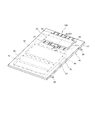
- FIG. 4 is a perspective view for explaining a state in which the power module is disposed on the cooler.
- FIG. 5 is a circuit diagram of a power module.
- FIG. 6 is a perspective view of the power module seen through the insulating mold portion.
- FIG. 7 is a perspective perspective view of the power module seen through the insulating mold portion.
- FIG. 8 is a plan perspective view of the power module.
- FIG. 6 is a perspective view of the power module seen through the insulating mold portion.
- FIG. 7 is a perspective perspective view of the power module seen through the insulating mold portion.
- FIG. 8 is a plan perspective view of the power module
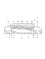
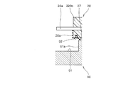
- FIG. 9A is a cross-sectional view of the semiconductor device according to the first embodiment of the present invention, showing a cross-section along the line IXA-IXA in FIG.
- FIG. 9B is a diagram showing the spatial distance between the cooler and the terminal in the semiconductor device shown in FIG. 9A.
- FIG. 9C is a diagram showing a creeping distance between a cooler and a terminal in the semiconductor device shown in FIG. 9A.
- FIG. 10A is a cross-sectional view of a semiconductor device according to a second embodiment of the present invention.
- FIG. 10B is a diagram showing the spatial distance between the cooler and the terminal in the semiconductor device shown in FIG. 10A.
- FIG. 10C is a diagram showing a creeping distance between a cooler and a terminal in the semiconductor device shown in FIG.
- FIG. 11A is a cross-sectional view of a semiconductor device according to a modification of the second embodiment of the present invention.
- 11B is a diagram showing the spatial distance between the cooler and the terminal in the semiconductor device shown in FIG. 11A.
- FIG. 11C is a diagram showing a creeping distance between a cooler and a terminal in the semiconductor device shown in FIG. 11A.
- FIG. 12A is a cross-sectional view of a semiconductor device according to a third embodiment of the present invention.
- 12B is a diagram showing the spatial distance between the cooler and the terminal in the semiconductor device shown in FIG. 12A.
- 12C is a diagram showing a creeping distance between a cooler and a terminal in the semiconductor device shown in FIG. 12A.
- FIG. 12A is a cross-sectional view of a semiconductor device according to a modification of the second embodiment of the present invention.
- 11B is a diagram showing the spatial distance between the cooler and the terminal in the semiconductor device shown in FIG. 11A.
- FIG. 13A is a cross-sectional view of a semiconductor device according to a modification of the third embodiment of the present invention.
- FIG. 13B is a diagram showing the spatial distance between the cooler and the terminal in the semiconductor device shown in FIG. 13A.
- FIG. 13C is a diagram showing a creeping distance between a cooler and a terminal in the semiconductor device shown in FIG. 13A.
- FIG. 14A is a cross-sectional view taken along line XIVA-XIVA in FIG. 14B is a cross-sectional view taken along line XIVB-XIVB in FIG.
- FIG. 15 is a plan view of the conductive plate in the power module.
- FIG. 16 is a plan view of the conductive plate in the power module according to the first modification.
- FIG. 17 is a plan view of a conductive plate in a power module according to a second modification.
- FIG. 18 is a plan view of a conductive plate in a power module according to a third modification.
- FIG. 19 is a plan view of a conductive plate in a power module according to a fourth modification.
- FIG. 20 is a plan view of a conductive plate in a power module according to a fifth modification.
- FIG. 21 is an enlarged plan view of the vicinity of the U phase of the conductive plate in the power module according to the sixth modification.
- FIG. 22 is an enlarged plan view of the vicinity of the U phase of the conductive plate in the power module according to the seventh modification.
- the power conversion device 1 is mounted on an electric vehicle or a plug-in hybrid vehicle (electric vehicle), and drives a motor generator (load) 6 as a rotating electric machine with DC power of a battery (electric storage device) 5. Convert to AC power suitable for Motor generator 6 is driven by the power supplied from power conversion device 1.
- the power conversion device 1 converts the regenerative power (AC power) of the motor generator 6 into DC power to charge the battery 5.
- the power conversion device 1 charges the battery 5 by being supplied with electric power from an external connector (not shown) for charging provided in the vehicle via the quick charging connector 63 or the normal charging connector 81.
- the battery 5 is formed of, for example, a lithium ion secondary battery.
- the battery 5 supplies DC power to the power conversion device 1 and is charged by the DC power supplied from the power conversion device 1.
- the voltage of the battery 5 fluctuates, for example, between 240 V and 400 V, and is charged when a higher voltage is input.
- the motor generator 6 is configured of, for example, a permanent magnet synchronous motor. Motor generator 6 is driven by AC power supplied from power conversion device 1. The motor generator 6 rotationally drives drive wheels (not shown) of the vehicle when the vehicle is driven. The motor generator 6 functions as a generator when the vehicle decelerates, and generates regenerative power.
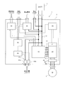
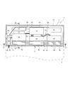
- the power converter device 1 is provided with the box-shaped case 2 which has the bottom part (installation part) 2c.
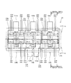
- the power conversion device 1 includes a capacitor module (smoothing capacitor) 10, a power module 20, a DC / DC converter 30, a charging device 40, a charging / DC / DC controller 50, and an inverter controller 70 in a case 2. These parts are electrically connected by bus bars or wires.
- the case 2 is configured of a lower case 2 b whose upper surface is open and an upper case 2 a which closes the opening of the lower case 2 b.
- a power module 20, a DC / DC converter 30, and a charging device 40 are provided in contact with the cooling surface 2d of the bottom 2c.
- the lower case 2 b has a cooling water channel (cooling medium channel) 4. Cooling water (cooling medium) flows through the cooling water flow path 4. Cooling water channel 4 is formed inside bottom 2c. The cooling water flowing through the cooling water flow path 4 cools the power module 20 mounted on the cooling surface 2 d immediately above the cooling water flow path 4, the DC / DC converter 30, and the charging device 40. Cooling water channel 4 is formed along power module cooling unit 4 a formed along power module 20, DC / DC converter cooling unit 4 b along DC / DC converter 30, and charging device 40. And a charging device cooling unit 4c.
- the outer surface of the bottom 2 c of the lower case 2 b faces the motor generator 6.
- the bottom 2c of the lower case 2b has a through hole 3 through which an output bus bar (bus bar module) 24 described later is inserted.
- the through hole 3 is formed outside the area where the cooling water flow path 4 is formed in the lower case 2 b. Therefore, as compared with the case where the through hole 3 is formed in the region where the cooling water flow path 4 is formed, there is no need to provide a seal or the like for the through hole 3, so the lower case 2 b can be miniaturized and cooling Water sealability can be secured.
- the capacitor module 10 is attached to the lower case 2 b so as to straddle the upper side of the DC / DC converter 30. In FIG. 3, the legs of the capacitor module 10 attached to the lower case 2b are omitted.
- the capacitor module 10 is configured of a plurality of capacitor elements.
- the capacitor module 10 smoothes, for example, the voltage of the DC power supplied from the battery 5 and the voltage of the regenerated power regenerated from the motor generator 6 via the power module 20. Thus, the capacitor module 10 removes noise and suppresses voltage fluctuations by smoothing the voltage.
- the capacitor module 10 includes a first bus bar 11, a second bus bar 12, and a power wiring 13.
- a power module 20, a DC / DC converter 30, and a charging device 40 are disposed around the capacitor module 10.
- the capacitor module 10 is disposed inside the case 2 between the power module 20 and the charging device 40.
- the capacitor module 10 is stacked on the DC / DC converter 30, and the DC / DC converter 30 is disposed below the capacitor module 10.
- the charging device 40 is stacked on the charging / DC / DC controller 50, and the charging device 40 is disposed below the charging / DC / DC controller 50.
- the first bus bar 11 protrudes laterally from one side surface of the capacitor module 10 and is connected to the power module 20.
- the power module 20 is directly connected to the first bus bar 11 by screwing or the like.
- the second bus bar 12 is connected to the DC / DC converter 30, the relay 61, the battery 5, and the electric compressor (not shown) (see FIG. 1).
- the power wiring 13 is connected to the charging device 40.
- the first bus bar 11, the second bus bar 12, and the power wiring 13 share the positive electrode and the negative electrode inside the capacitor module 10.
- the second bus bar 12 protrudes downward from the bottom surface of the capacitor module 10.
- the second bus bar 12 is directly screwed to a DC / DC converter 30 which is disposed to be stacked below the capacitor module 10.
- the second bus bar 12 is connected to the positive relay 61 a and the negative relay 61 b.
- the second bus bar 12 is connected via the bus bar 14 to the battery side connector 51 connected to the battery 5 and the compressor side connector 52 connected to the electric compressor.
- the power wiring 13 is drawn to the side.
- the power wiring 13 is a flexible cable having flexibility and is connected to the charging device 40.
- the charging device 40 is connected to the normal charging connector 81 via the bus bar 41.
- the signal line connector 65 enables the signal line 55 connected to the DC / DC converter 30, the charging device 40, the charging / DC / DC controller 50, and the inverter controller 70 to be connected to the outside of the case 2.
- the signal line 55 connects the signal line connector 65 and the charging / DC / DC controller 50.
- the signal line 55 is bundled with the signal line 62 leading from the charge / DC / DC controller 50 to the relay controller 60, passes through the top surface of the capacitor module 10, and is connected to the connector 56 of the charge / DC / DC controller 50. .
- a plurality of guide portions 58 supporting the signal lines 55 and the signal lines 62 are formed on the top surface of the capacitor module 10.
- the power module 20 has IGBTs (Insulated Gate Bipolar Transistors) 28 u, 29 u, 28 v, 29 v, 28 w, 29 w (see FIG. 5) as a plurality of power elements (semiconductor elements).
- the power module 20 mutually converts the DC power of the battery 5 and the AC power of the motor generator 6 by switching ON / OFF switching of the IGBTs 28 u to 29 w.
- the IGBTs 28 u to 29 w are controlled to be turned on / off by a driver substrate 21 provided in the power module 20.
- the driver substrate 21 is stacked on the upper surface of the power module 20.
- An inverter controller 70 and a relay controller 60 are disposed above the driver substrate 21.
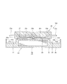
- the power module 20 is connected to the first bus bar 11 of the capacitor module 10. Connected to the power module 20 is a three-phase output bus bar 24 composed of a U-phase, a V-phase, and a W-phase.
- output bus bar 24 detects the current of power module terminal 25 connected to power module 20, motor terminal (load terminal) 26 connected to motor generator 6, and output bus bar 24. And a sensor 22.
- the output bus bar 24 is connected to the opposite side of the first bus bar 11 in the power module 20.
- Output bus bar 24 is directly connected to each of the U-phase, V-phase, and W-phase of power module 20, and outputs three-phase AC power to motor generator 6.
- the power module terminals 25 and the motor terminals 26 are formed in directions intersecting each other. Specifically, motor terminal 26 is connected to motor generator 6 disposed below output bus bar 24. The power module terminal 25 is connected to the power module 20 disposed on the side of the output bus bar 24. Thus, the motor terminals 26 are formed to intersect the power module terminals 25 at a right angle.
- Output bus bar 24 is accommodated in case 2.
- the tip of the motor terminal 26 is inserted through the through hole 3 of the bottom 2 c of the case 2 and exposed to the outside.
- the motor terminal 26 can be connected to the motor generator 6 via a harness or the like (not shown).
- the inverter controller 70 operates the power module 20 based on the instruction from the controller (not shown) of the vehicle and the detection result of the U phase, V phase and W phase currents from the current sensor 22.
- the driver signal is output to the driver substrate 21.
- the driver board 21 controls the power module 20 based on the signal from the inverter controller 70.
- the inverter controller 70, the driver board 21, the power module 20, and the capacitor module 10 constitute an inverter module that mutually converts DC power and AC power.
- the DC / DC converter 30 is provided to face the output bus bar 24 with the power module 20 interposed therebetween.
- the DC / DC converter 30 is connected to the vehicle side connector 82 via the bus bar 31.
- the vehicle side connector 82 is connected to a harness or the like that supplies DC power output from the DC / DC converter 30 to each part of the vehicle.
- the DC / DC converter 30 converts the voltage of the DC power supplied from the battery 5 and supplies it to other devices when the vehicle is driven (when the power module 20 is driven) or stopped.
- the DC / DC converter 30 steps down DC power (for example, 400 V) of the battery 5 to 12 V DC power.
- the stepped-down DC power is supplied as a power supply for a controller provided in the vehicle, lighting, a fan, and the like.
- the DC / DC converter 30 is connected to the capacitor module 10 and the battery 5 via the second bus bar 12.
- the charging device 40 is provided to face the power module 20 with the DC / DC converter 30 interposed therebetween.
- the charging device 40 converts an external power supply (for example, AC 100 V or 200 V) supplied from an external connector for charging provided in the vehicle via the normal charging connector 81 into DC power (for example 500 V).
- the direct current power converted by the charging device 40 is supplied from the power wiring 13 to the battery 5 via the capacitor module 10. Thereby, the battery 5 is charged.
- the charge / DC / DC controller 50 controls the drive of the motor generator 6 by the power conversion device 1 and the charge of the battery 5. Specifically, the charging / DC / DC controller 50 charges the battery 5 by the charging device 40 via the normal charging connector 81 and the battery 5 via the rapid charging connector 63 based on an instruction from the controller of the vehicle. Control of the charging of the motor generator 6 and the driving of the motor generator 6.
- the relay controller 60 is controlled by the charging / DC / DC controller 50 to control the on / off of the relay 61.
- the relay 61 is composed of a positive relay 61 a and a negative relay 61 b.
- the relay 61 is connected when the external connector for charging provided in the vehicle is connected via the rapid charging connector 63, and direct current power (eg, 500 V) supplied from the rapid charging connector 63 to the second bus bar 12 Supply.
- the battery 5 is charged by the supplied DC power.
- the semiconductor devices 100, 200, and 300 according to the first to third embodiments of the present invention will be described below with reference to FIGS. 4 to 13C.
- the semiconductor device 100 includes a power module 20 and a cooler 90 which is formed in a part of the lower case 2 b and cools the power module 20.
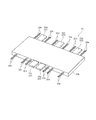
- the power module 20 includes IGBTs 28u to 29w and a resin mold portion 20b as an insulation mold portion surrounding the IGBTs 28u to 29w.
- the resin mold portion 20b is molded by transfer molding using a nonconductive resin.
- Power module 20 is connected to IGBTs 28u to 29w, and is a positive (upper) bus bar 23a, a negative (lower) bus bar 23b, a U-phase bus bar 23u, and a V-phase bus bar 23v as terminals projecting laterally to resin mold portion 20b. , W phase bus bars 23w.
- the positive electrode bus bar 23 a and the negative electrode bus bar 23 b are drawn out from the same side surface of the resin mold portion 20 b and connected to the capacitor module 10 via the first bus bar 11.
- U-phase bus bar 23u, V-phase bus bar 23v and W-phase bus bar 23w are drawn out from the side opposite to the side from which positive electrode bus bar 23a and negative electrode bus bar 23b of resin molded portion 20b are drawn.
- Connected to 25 Connected to 25
- the power module 20 converts DC power into AC power. Specifically, power module 20 is mounted on a vehicle (not shown), converts DC power of battery 5 into AC power, and supplies it to motor generator 6. The power module 20 also converts the regenerative power (AC power) of the motor generator 6 into DC power so that the battery 5 can be charged. As described above, the power module 20 mutually converts DC power and AC power.
- the power module 20 includes a plurality of switching elements 28 u to 29 w each including a set of an upper arm and a lower arm corresponding to each of U phase, V phase, and W phase, and each switching element 28 u to It includes a diode 20c connected in parallel to 29w, and a resin mold portion 20b (see FIG. 6) surrounding the switching elements 28u to 29w and the diode 20c.
- the power module 20 includes switching elements 28u and 29u corresponding to the U phase, switching elements 28v and 29v corresponding to the V phase, and switching elements 28w and 29w corresponding to the W phase.
- the power module 20 includes bus bars 23 as a plurality of conductive plates.
- the bus bar 23 includes a positive electrode bus bar 23a, a negative electrode bus bar 23b, a U-phase bus bar 23u, a V-phase bus bar 23v, and a W-phase bus bar 23w connected to the respective switching elements 28u to 29w.
- the resin mold portions 20 b mutually insulate between the bus bars 23.
- U-phase bus bar 23u, V-phase bus bar 23v, and W-phase bus bar 23w are the first conductive plate
- positive bus bar 23a is the second conductive plate
- negative bus bar 23b is the third conductive plate.
- a plurality of (three) first conductive plates are provided corresponding to each phase (three phases).
- a signal line 20d to which a signal for controlling switching is input / output, and a signal line 20e to which signals of a temperature sensor and a current sensor are input / output are connected.
- the signal lines 20d and 20e and the bus bar 23 protrude to the side of the resin mold portion 20b.
- the positive electrode bus bar 23a and the negative electrode bus bar 23b are connected to a battery side bus bar (not shown).
- U-phase bus bar 23 u, V-phase bus bar 23 v, and W-phase bus bar 23 w are connected to the motor generator via an output bus bar (not shown).
- the power module 20 is formed in a thin plate-like rectangular shape. From the first side surface of the power module 20, the positive electrode bus bar 23a and the negative electrode bus bar 23b protrude. A U-phase bus bar 23 u, a V-phase bus bar 23 v, and a W-phase bus bar 23 w protrude from a second side surface located on the opposite side of the first side surface of the power module 20.
- the signal lines 20d and 20e are respectively the first side surfaces from which the positive electrode bus bars 23a and the negative electrode bus bars 23b protrude, or the second side surfaces from which the U phase bus bars 23u, the V phase bus bars 23v, and the W phase bus bars 23w protrude. Project in the same direction as.
- the positive electrode bus bar 23 a, the negative electrode bus bar 23 b, the U-phase bus bar 23 u, the V-phase bus bar 23 v, and the W-phase bus bar 23 w protrude from substantially the same position in the thickness direction of the power module 20.
- the power module 20 has a thin plate shape. In the power module 20, switching elements 28u to 29w and a diode 20c are arranged in alignment.
- One switching element in the circuit diagram of FIG. 5 is actually configured by a pair of switching elements connected in parallel.
- one diode in the circuit diagram of FIG. 5 is actually constituted by a pair of diodes connected in parallel.
- the U-phase, V-phase, and W-phase each consist of an upper arm consisting of two switching elements and two diodes, and a lower arm consisting of two switching elements and two diodes. ing. These switching elements and diodes are all arranged on a plane in the power module 20.
- the upper arm (positive electrode side) of the U phase is composed of two switching elements 28u-1 and 28u-2 and two diodes 20c-u1 and 20c-u2.
- the lower arm (negative electrode side) of the U phase is composed of two switching elements 29u-1 and 29u-2 and two diodes 20c-u3 and 20c-u4.
- Switching elements 29u-1 and 29u-2 are arranged in the longitudinal direction of resin mold portion 20b.
- the diodes 20c-u3 and 20c-u4 are disposed between the two switching elements 29u-1 and 29u-2, and are disposed side by side in the lateral direction of the resin mold portion 20b.
- switching elements 28u-1 and 28u-2 are arranged side by side in the longitudinal direction of resin mold portion 20b.
- the diodes 20c-u1 and 20c-u2 are disposed between the two switching elements 28u-1 and 28u-2, and are disposed side by side in the lateral direction of the resin mold portion 20b.
- U-phase bus bar 23 u includes a terminal portion 100 u as an AC terminal protruding from the side surface of resin mold portion 20 b.
- Two switching elements 29u-1 and 29u-2 and two diodes 20c-u3 and 20c-u4 are mounted on U-phase bus bar 23u (see FIGS. 14A and 14B).
- Switching elements 29u-1 and 29u-2 and diodes 20c-u3 and 20c-u4 are interposed between U-phase bus bar 23u and negative electrode bus bar 23b. That is, the collector sides of the switching elements 29u-1 and 29u-2 are connected to the U-phase bus bar 23u, and the emitter sides of the switching elements 29u-1 and 29u-2 are connected to the negative bus bar 23b.
- Such switching elements 29u-1 and 29u-2 switch conduction of power between the U-phase bus bar 23u and the negative electrode bus bar 23b as the switching elements 29u of the U-phase lower arm.
- the terminal portion 100u of the U-phase bus bar 23u protrudes in the outward direction of the resin mold portion 20b from the position of the diodes 20c-u3 and 20c-u4 placed between the two switching elements 29u-1 and 29u-2.
- Signal lines 20d and 20e are connected to the switching elements 29u-1 and 29u-2 respectively by bonding wires or the like.
- the signal lines 20d and 20e protrude in the outward direction of the resin mold portion 20b at positions close to both sides in the longitudinal direction of the terminal portion 100u of the U-phase bus bar 23u.
- two switching elements 28u-1 and 28u-2 are disposed in the longitudinal direction, and two diodes 20c-u1 and 20c-u2 are disposed in the lateral direction, and are respectively mounted on positive electrode bus bars 23a See FIGS. 14A and 14B.
- Switching elements 28u-1 and 28u-2 and diodes 20c-u1 and 20c-u2 are interposed between positive electrode bus bar 23a and U-phase bus bar 23u. That is, the collector sides of the switching elements 28u-1 and 28u-2 are connected to the positive electrode bus bar 23a, and the emitter sides of the switching elements 28u-1 and 28u-2 are connected to the U-phase bus bar 23u.
- Such switching elements 28u-1 and 28u-2 switch conduction of electric power between the positive electrode bus bar 23a and the U phase bus bar 23u as the switching element 28u of the upper arm of the U phase.
- Signal lines 20d and 20e are connected to the switching elements 28u-1 and 28u-2, respectively.
- the signal lines 20d and 20e protrude in the outward direction of the resin mold portion 20b from the surface opposite to the surface on which the terminal portion 100u of the U-phase bus bar 23u is provided.
- the V-phase upper arm (positive electrode side) is composed of two switching elements 28v-1 and 28v-2 and two diodes 20c-v1 and 20c-v2.
- the lower arm (negative electrode side) of the V phase is composed of two switching elements 29 v-1 and 29 v-2 and two diodes 20 c-v 3 and 20 c-v 4.
- Switching elements 29 v-1 and 29 v-2 are arranged side by side in the longitudinal direction of resin mold portion 20 b.
- the diodes 20c-v3 and 20c-v4 are disposed between the two switching elements 29v-1 and 29v-2, and two diodes 20c-v3 and 20c-v4 are disposed side by side in the lateral direction of the resin mold portion 20b.
- switching elements 28 v-1 and 28 v-2 are arranged side by side in the longitudinal direction of resin mold portion 20 b.
- the diodes 20c-v1 and 20c-v2 are disposed between the two switching elements 28v-1 and 28v-2, and are disposed side by side in the lateral direction of the resin mold portion 20b.
- V-phase bus bar 23v includes a terminal portion 100v as an AC terminal protruding from the side surface of resin mold portion 20b.
- Two switching elements 29v-1 and 29v-2 and two diodes 20c-v3 and 20c-v4 are mounted on the V-phase bus bar 23v.
- Switching elements 29 v-1 and 29 v-2 and diodes 20 c-v 3 and 20 c-v 4 are interposed between V-phase bus bar 23 v and negative electrode bus bar 23 b. That is, the collector sides of the switching elements 29v-1 and 29v-2 are connected to the V-phase bus bar 23v, and the emitter sides of the switching elements 29v-1 and 29v-2 are connected to the negative bus bar 23b.
- Such switching elements 29 v-1 and 29 v-2 switch power conduction between the V-phase bus bar 23 v and the negative bus bar 23 b as the switching element 29 v of the V-phase lower arm.
- the terminal portion 100v of the V-phase bus bar 23v protrudes in the outward direction of the resin mold portion 20b from the position of the diodes 20c-v3 and 20c-v4 disposed between the two switching elements 29v-1 and 29v-2.
- Signal lines 20d and 20e are connected to the switching elements 29v-1 and 29v-2, respectively.
- the signal lines 20d and 20e protrude outward of the resin mold portion 20b at positions close to both sides in the longitudinal direction of the terminal portion 100v of the V-phase bus bar 23v.
- switching elements 28v-1 and 28v-2 are disposed in the longitudinal direction, and two diodes 20c-v1 and 20c-v2 are disposed in the lateral direction, and mounted on positive bus bar 23a.
- Switching elements 28 v-1 and 28 v-2 and diodes 20 c-v 1 and 20 c-v 2 are interposed between positive electrode bus bar 23 a and V-phase bus bar 23 v. That is, the collector sides of the switching elements 28v-1 and 28v-2 are connected to the positive electrode bus bar 23a, and the emitter sides of the switching elements 28v-1 and 28v-2 are connected to the V-phase bus bar 23v.
- Such switching elements 28 v-1 and 28 v-2 switch power conduction between the positive electrode bus bar 23 a and the V-phase bus bar 23 v as the switching element 28 v of the V-phase upper arm.
- Signal lines 20d and 20e are connected to the switching elements 28v-1 and 28v-2, respectively.
- the signal lines 20d and 20e protrude outward of the resin mold portion 20b from the surface opposite to the surface on which the terminal portion 100v of the V-phase bus bar 23v is protruded.
- the terminal portion 120a as a direct current positive electrode terminal of the positive electrode bus bar 23a and the terminal portion 120b as a direct current negative electrode terminal of the negative electrode bus bar 23b are resin molded portions It projects in the outward direction of 20b.
- the signal lines 20d and 20e connected to the switching elements 28v-1 and 28v-2 are offset in the longitudinal direction of the resin mold portion 20b, avoiding the terminal portion 120a of the positive electrode bus bar 23a and the terminal portion 120b of the negative electrode bus bar 23b.
- the upper arm (positive electrode side) of the W phase is composed of two switching elements 28w-1 and 28w-2 and two diodes 20c-w1 and 20c-w2.
- the lower arm (negative electrode side) of the W phase is composed of two switching elements 29w-1 and 29w-2 and two diodes 20c-w3 and 20c-w4.
- the switching elements 29w-1 and 29w-2 are arranged in the longitudinal direction of the resin mold portion 20b.
- the diodes 20c-w3 and 20c-w4 are disposed between the two switching elements 29w-1 and 29w-2, and two diodes 20c-w3 and 20c-w4 are disposed side by side in the lateral direction of the resin mold portion 20b.
- two switching elements 28w-1 and 28w-2 are arranged side by side in the longitudinal direction of the resin mold portion 20b.
- the diodes 20c-w1 and 20c-w2 are disposed between the two switching elements 28w-1 and 28w-2, and two diodes 20c-w1 and 20c-w2 are disposed side by side in the lateral direction of the resin mold portion 20b.
- W-phase bus bar 23 w includes a terminal portion 100 w as an AC terminal protruding from the side surface of resin mold portion 20 b.
- Two switching elements 29w-1 and 29w-2 and two diodes 20c-w3 and 20c-w4 are mounted on the W-phase bus bar 23w.
- Switching elements 29w-1 and 29w-2 and diodes 20c-w3 and 20c-w4 intervene between W-phase bus bar 23w and negative electrode bus bar 23b. That is, the collector sides of the switching elements 29w-1 and 29w-2 are connected to the W-phase bus bar 23w, and the emitter sides of the switching elements 29w-1 and 29w-2 are connected to the negative bus bar 23b.
- Such switching elements 29w-1 and 29w-2 switch the conduction of electric power between the W-phase bus bar 23w and the negative electrode bus bar 23b as the switching element 29w of the lower arm of the W-phase.
- the terminal portion 100w of the W-phase bus bar 23w protrudes in the outward direction of the resin mold portion 20b from the position of the diodes 20c-w3 and 20c-w4 placed between the two switching elements 29w-1 and 29w-2.
- Signal lines 20d and 20e are connected to the switching elements 29w-1 and 29w-2, respectively.
- the signal lines 20d and 20e protrude outward of the resin mold portion 20b at positions close to both sides in the longitudinal direction of the terminal portion 100w of the W-phase bus bar 23w.
- two switching elements 28w-1 and 28w-2 are disposed in the longitudinal direction, and two diodes 20c-w1 and 20c-w2 are disposed in the lateral direction, and mounted on positive bus bar 23a, respectively. Ru.
- the switching elements 28w-1 and 28w-2 and the diodes 20c-w1 and 20c-w2 are interposed between the positive electrode bus bar 23a and the W-phase bus bar 23w. That is, the collector sides of the switching elements 28w-1 and 28w-2 are connected to the positive electrode bus bar 23a, and the emitter sides of the switching elements 28w-1 and 28w-2 are connected to the W-phase bus bar 23w.
- Such switching elements 28w-1 and 28w-2 switch the conduction of power between the positive electrode bus bar 23a and the W phase bus bar 23w as the switching element 28w of the upper arm of the W phase.
- Signal lines 20d and 20e are connected to the switching elements 28w-1 and 28w-2, respectively.
- the signal lines 20d and 20e protrude outward of the resin mold portion 20b from the surface opposite to the surface on which the terminal portion 100w of the W-phase bus bar 23w is provided.
- the positive electrode bus bar 23a, the U-phase bus bar 23u, the V-phase bus bar 23v, and the W-phase bus bar 23w are partially surrounded by the bottom of the resin mold 20b without being completely surrounded by the resin mold 20b. Is exposed.
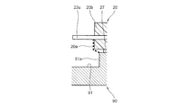
- the power module 20 is mounted on the cooler 90 via the insulating sheet 27.
- the positive electrode bus bar 23a exposed from the resin mold portion 20b, the U-phase bus bar 23u, the V-phase bus bar 23v, and the W-phase bus bar 23w are in contact with the insulating sheet 27.
- the insulating sheet 27 is formed of a nonconductive material such as ceramic or resin. By providing the insulating sheet 27, even if the positive electrode bus bar 23a, the U phase bus bar 23u, the V phase bus bar 23v, and the W phase bus bar 23w are not completely surrounded by the resin mold portion 20b, insulation between the positive electrode bus bar 23a It is possible to secure the sex.
- the cooler 90 is made of a metal material (conductive material) such as aluminum.
- the positive electrode bus bar 23 a is connected to the positive electrode of the battery 5.
- Negative electrode bus bar 23 b is connected to the negative electrode of battery 5.
- the positive electrode bus bar 23 a and the negative electrode bus bar 23 b are connected in parallel to the capacitor module 10.
- U-phase bus bar 23u, V-phase bus bar 23v, and W-phase bus bar 23w are connected to U-phase, V-phase, and W-phase of motor generator 6 via output bus bar 24, respectively.
- each of the IGBTs 28u to 29w has a diode 20c as a free wheeling diode connected in parallel in the reverse direction.
- the IGBTs 28 u to 29 w are respectively provided with a signal line (gate signal lead) 20 d for performing switching control and a signal line (emitter signal lead) 20 e for detecting a reference voltage on the emitter side.
- the IGBT 28 u and the IGBT 29 u are provided in series with the U-phase bus bar 23 u interposed between the positive electrode bus bar 23 a and the negative electrode bus bar 23 b.
- U-phase bus bar 23 u is connected to a coil (not shown) forming the U-phase of motor generator 6 via output bus bar 24.
- the IGBT 28 v and the IGBT 29 v are provided in series between the positive bus bar 23 a and the negative bus bar 23 b with the V phase bus bar 23 v interposed therebetween.
- V-phase bus bar 23 v is connected to a coil (not shown) constituting V-phase of motor generator 6 via output bus bar 24.
- the IGBT 28 w and the IGBT 28 w are provided in series with the W-phase bus bar 23 w interposed between the positive electrode bus bar 23 a and the negative electrode bus bar 23 b.
- W-phase bus bar 23 w is connected to a coil (not shown) constituting W-phase of motor generator 6 via output bus bar 24.
- the power modules 20 generate switching currents to drive the motor generator 6 by the switching control of the IGBTs 28 u to 29 w by the driver substrate 21.
- the power modules 20 convert the regenerative power from the motor generator 6 from alternating current to direct current and charge the battery 5 by the switching control of the IGBTs 28 u to 29 w by the driver substrate 21.
- the cooler 90 cools the IGBTs 28u to 29w from the bottom of the resin mold portion 20b.
- the cooler 90 has a power module cooling unit 4a which is a part of the cooling water flow path 4 provided inside the lower case 2b and through which the cooling water flows.
- the power module 20 is cooled by heat exchange with the cooling water flowing in the power module cooling unit 4a.
- the IGBTs 28 u to 29 w are arranged such that the surface constituting the collector faces the cooler 90. Thereby, IGBTs 28u to 29w can be cooled from the collector side.
- the cooler 90 includes a power module cooling unit (first cooling medium flow path) 4 a for circulating cooling water to cool the power module 20, and a cooling water for circulating the cooling module. And a DC / DC converter cooling unit (second cooling medium flow path) 4 b for cooling the DC / DC converter 30 as another device.
- the cooler 90 has a pair of concave portions 91 formed in a concave shape from the surface where the power module 20 is installed at a position facing the positive electrode bus bar 23a, the negative electrode bus bar 23b, the U phase bus bar 23u, the V phase bus bar 23v, and the W phase bus bar 23w. Have.
- one concave portion 91 facing the positive electrode bus bar 23a and the negative electrode bus bar 23b is formed in a groove shape between the power module cooling portion 4a and the DC / DC converter cooling portion 4b.
- the other recess 91 facing the U-phase bus bar 23 u, the V-phase bus bar 23 v, and the W-phase bus bar 23 w is formed in a groove shape between the power module cooling portion 4 a and the output bus bar 24. Therefore, since the concave portion 91 is formed in the portion where the cooling water flow path 4 is not provided, the space of the bottom portion 2 c can be effectively utilized, and the bottom portion 2 c is compared with the case where the concave portion 91 is formed Can be prevented from becoming thick.
- the inner end portion 91a of the recess 91 is formed to be located inside the end portion 20a of the resin mold portion 20b. Further, the outer end portion 91b of the recess 91 is formed outside the tips of the positive electrode bus bar 23a, the negative electrode bus bar 23b, the U phase bus bar 23u, the V phase bus bar 23v, and the W phase bus bar 23w. That is, the recess 91 is formed from the position facing the positive electrode bus bar 23a, the negative electrode bus bar 23b, the U phase bus bar 23u, the V phase bus bar 23v, and the W phase bus bar 23w from the end 91a of the resin mold 20b.
- the cooler 90 and the positive electrode bus bar 23a, the negative electrode bus bar 23b, the U phase bus bar 23u, the V phase bus bar 23v, and the W phase bus bar 23w as compared with the case where the recess 91 is not provided.
- the creepage distance increases. Therefore, the spatial distance (the distance shown by the broken line in FIG. 9B) between the cooler 90 and the positive electrode bus bar 23a, the negative electrode bus bar 23b, the U phase bus bar 23u, the V phase bus bar 23v, and the W phase bus bar 23w can be secured. The insulation can be improved.
- the power module 20 is thinned, and the resin mold portion 20b is formed by transfer molding to form the positive bus bar 23a, the negative bus bar 23b, the U phase bus bar 23u, the V phase bus bar 23v, and the W phase. Even in the case where the bus bar 23 w protrudes to the side of the resin mold portion 20 b, electrical insulation can be ensured.
- the cooler 90 for cooling the IGBTs 28u to 29w from the bottom of the resin mold portion 20b is a portion of the resin mold portion 20b from the position facing the positive electrode bus bar 23a, the negative electrode bus bar 23b, the U phase bus bar 23u, the V phase bus bar 23v and the W phase bus bar 23w.
- a recess 91 is provided inward of the end 20a.
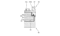
- FIGS. 10A to 11C The semiconductor device 200 according to the second embodiment of the present invention will be described below with reference to FIGS. 10A to 11C.
- points different from the first embodiment are mainly described, and the configurations having the same functions are denoted with the same reference numerals and the description thereof is omitted.
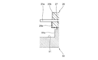
- the shape of the resin mold portion 220b is different from that of the resin mold portion 20b of the first embodiment.
- the resin mold portion 220b further includes a pair of concave portions 92 formed in a concave shape from the surface facing the concave portion 91 of the cooler 90.
- the recess 92 is formed in a groove shape so as to face the recess 91 of the cooler 90.
- the creepage distance (the distance shown by the broken line in FIG. 10C) between the cooler 90 and the positive electrode bus bar 23a, the negative electrode bus bar 23b, the U phase bus bar 23u, the V phase bus bar 23v, and the W phase bus bar 23w further increases. Therefore, it is possible to secure a spatial distance (a distance shown by a broken line in FIG. 10B) between the cooler 90, the positive electrode bus bar 23a, the negative electrode bus bar 23b, the U phase bus bar 23u, the V phase bus bar 23v, and the W phase bus bar 23w. It is possible to improve the quality.
- FIG. 11A you may provide the terminal block 93 in the recessed part 91 of the cooler 90.
- FIG. The terminal block 93 is provided between the recess 91 and the positive electrode bus bar 23a, the negative electrode bus bar 23b, the U phase bus bar 23u, the V phase bus bar 23v, and the W phase bus bar 23w, and the positive electrode bus bar 23a, the negative electrode bus bar 23b, and the U phase bus bar 23u , V-phase bus bars 23v, and W-phase bus bars 23w.
- the positive bus bar 23 a and the negative bus bar 23 b are fastened to the first bus bar 11 with a bolt on the top surface of the terminal block 93.
- the U-phase bus bar 23 u, the V-phase bus bar 23 v, and the W-phase bus bar 23 w are fastened to the power module terminal 25 of the output bus bar 24 with a bolt on the top surface of the terminal block 93.
- the terminal block 93 has a convex portion 93a inserted into the concave portion 92 of the resin mold portion 220b.
- the convex portion 93a is inserted into the concave portion 92, and between the cooler 90 and the positive electrode bus bar 23a, the negative electrode bus bar 23b, the U phase bus bar 23u, the V phase bus bar 23v, and the W phase bus bar 23w. Space distance (the distance shown by a broken line in FIG. 11B) is further increased.
- the cooler 90, the positive electrode bus bar 23a, the negative electrode bus bar 23b, the U phase bus bar 23u, the V phase bus bar 23v, and the W phase bus bar 23w Space distance and creepage distance between the The electrical insulation between the cooler 90 and the positive electrode bus bar 23a, the negative electrode bus bar 23b, the U phase bus bar 23u, the V phase bus bar 23v, and the W phase bus bar 23w can be further improved.
- the shape of the resin mold portion 320b is different from that of the resin mold portions 20b and 220b of the first and second embodiments.
- the resin mold portion 320b further includes a pair of concave portions 392 formed in a concave shape from the surface facing the concave portion 91 of the cooler 90.
- the recessed portion 92 is formed in a cutout shape at each corner of the bottom surface of the resin mold portion 320 b so as to face the recessed portion 91 of the cooler 90.
- the creepage distance (the distance shown by the broken line in FIG. 12C) between the cooler 90 and the positive electrode bus bar 23a, the negative electrode bus bar 23b, the U phase bus bar 23u, the V phase bus bar 23v, and the W phase bus bar 23w further increases. Therefore, the spatial distance (the distance shown by the broken line in FIG. 12B) between the cooler 90 and the positive electrode bus bar 23a, the negative electrode bus bar 23b, the U phase bus bar 23u, the V phase bus bar 23v, and the W phase bus bar 23w can be secured. The insulation can be improved.
- FIG. 13A you may provide the terminal block 393 in the recessed part 91 of the cooler 90.
- FIG. The terminal block 393 has a convex portion 393a inserted into the concave portion 92 of the resin mold portion 220b.
- the projection 393a is inserted into the recess 92, and between the cooler 90 and the positive electrode bus bar 23a, the negative electrode bus bar 23b, the U phase bus bar 23u, the V phase bus bar 23v, and the W phase bus bar 23w. Space distance (the distance shown by a broken line in FIG. 13B) is further increased.
- the cooler 90, the positive electrode bus bar 23a, the negative electrode bus bar 23b, the U phase bus bar 23u, the V phase bus bar 23v, and the W phase bus bar 23w Space distance and creepage distance between the The electrical insulation between the cooler 90 and the positive electrode bus bar 23a, the negative electrode bus bar 23b, the U phase bus bar 23u, the V phase bus bar 23v, and the W phase bus bar 23w can be further improved.
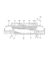
- FIG. 14A and FIG. 14B only the U phase bus bar 23 u is illustrated.
- V-phase bus bar 23v and W-phase bus bar 23w have a configuration similar to that of U-phase bus bar 23u.
- the U-phase bus bar 23 u will be described as an example, and the description of the V-phase bus bar 23 v and the W-phase bus bar 23 w will be appropriately omitted.
- switching element 28u-1 (and 28u-2) is sandwiched between positive electrode bus bar 23a and U-phase bus bar 23u, and is electrically connected to both bus bars.
- Signal lines 20d and 20e are connected to the switching element 28u-1 via bonding wires.
- switching element 29u-1 (and 29u-2) is sandwiched between negative bus bar 23b and U-phase bus bar 23u, and is electrically connected to both bus bars.
- Signal lines 20d and 20e are connected to the switching element 29u-1 through bonding wires.
- the diodes 20c-u1 and 20c-u2 are sandwiched between the positive electrode bus bar 23a and the U-phase bus bar 23u, and are electrically connected to both bus bars.
- diodes 20c-u3 and 20c-u4 are sandwiched between negative bus bar 23b and U-phase bus bar 23u, and are electrically connected to both bus bars.
- each switching element and diode have a thin shape, and they are arranged on a plane and held by each bus bar, so that the power module 20 can be formed thin. it can.
- the positive electrode bus bar 23a and the U-phase bus bar 23u are arranged such that their planes face each other.
- negative electrode bus bar 23b and U-phase bus bar 23u are arranged such that their planes face each other. That is, the positive electrode bus bar 23a, the negative electrode bus bar 23b, and the U-phase bus bar 23u are stacked such that the planes thereof face each other.
- the positive electrode bus bar 23a and the U-phase bus bar 23u may be disposed to face each other.
- the power module 20 at least two of the plurality of bus bars 23 are disposed to face each other.
- U-phase bus bar 23 u has a bent portion 233 u bent from a first portion 231 u facing the upper surface of positive electrode bus bar 23 a to a second portion 232 u having the same height as positive electrode bus bar 23 a.
- negative bus bar 23b is connected from a first portion 231b facing the top surface of first portion 231u of U-phase bus bar 23u to a second portion 232b having the same height as first portion 231u of U-phase bus bar 23u. It has a bending portion 233 b which bends.
- the positive electrode bus bar 23a also has a first portion 231a of the same height as the second portion 232u of the U-phase bus bar 23u.
- the second portion 232u of the U-phase bus bar 23u is connected to the switching elements (first switching elements) 29u-1 and 29u-2 and the diodes (first rectifying elements) 20c-u3 and 20c-u4. It corresponds to 1 junction.
- the first portion 231a of the positive electrode bus bar 23a is connected to the second junction where the switching elements (second switching elements) 28u-1 and 28u-2 and the diodes (second rectifying elements) 20c-u1 and 20c-u2 are joined.
- the bending portion 233 u is provided with a through hole 234 u penetrating in the thickness direction of the U-phase bus bar 23 u (direction facing the other bus bar 23).
- the through hole 234u is disposed between the first portion (first bonding portion) 231a and the second portion (second bonding portion) 232u.
- a through hole 234b penetrating in the thickness direction of the negative electrode bus bar 23b (the direction facing the other bus bar 23) is provided in the bent portion 233b.
- the through holes 234 u and 234 b are formed in both of the two bus bars 23 disposed opposite to each other.
- a part of the resin mold portion 20b is interposed from the through holes 234u and 234b, between the negative electrode bus bar 23b and the U phase bus bar 23u, and between the U phase bus bar 23u and the positive electrode bus bar 23a.
- the positive electrode bus bar 23a and the negative electrode bus bar 23b are disposed close to each other to enhance the proximity effect.
- a current flows in the opposite direction to the positive electrode bus bar 23a and the negative electrode bus bar 23b. Due to the proximity effect, mutual inductance is generated in the positive electrode bus bar 23a and the negative electrode bus bar 23b by mutually affecting the magnetic fields of the currents.
- the self-inductances of the positive electrode bus bar 23a and the negative electrode bus bar 23b cancel each other and are reduced. Therefore, the surge voltage at the time of switching is suppressed.
- the mold material which forms the resin mold part 20b is poured from upper direction.
- the positive electrode bus bar 23a, the U-phase bus bar 23u, and the negative electrode bus bar 23b are disposed close to each other, the molding material is unlikely to flow between them. Also, even if the molding material is poured from the side, since switching elements and diodes intervene between the bus bars, they become an obstacle.
- the through hole 234b is formed in the negative electrode bus bar 23b, and the through hole 234u is formed in the U-phase bus bar 23u. Therefore, the molding material flows between the negative electrode bus bar 23b and the U phase bus bar 23u through the through hole 234b, and further flows between the U phase bus bar 23u and the positive electrode bus bar 23a through the through hole 234u. Thereby, the molding material can be filled between the adjacent bus bars 23. Therefore, even if the bus bars 23 are arranged close to each other, the insulation state between each other can be secured.
- the through holes 234 b may be provided only in the negative electrode bus bar 23 b. Since the molding material is poured from the upper side, when the through holes are formed in only one of the bus bars 23 disposed opposite to each other, the through holes 234 b are formed in the upper side (in this case, the negative bus bar 23 b). The molding material can be filled between the adjacent bus bars 23. Thus, the through holes are provided in at least one of the two bus bars 23 disposed opposite to each other.
- the through hole 234u is provided in the bending portion 233u, and the through hole 234b is provided in the bending portion 233b.
- the mold material can be filled between the bent portion 233 u and the bent portion 233 b in which the mold material is relatively difficult to flow.
- press forming is performed in a state in which through holes 234u and 234b are formed, and bent portions 233u and 233b are formed on U phase bus bar 23u and negative electrode bus bar 23b. Therefore, bending is performed by the amount of through holes 234u and 234b. It is easier.
- a through hole may be provided in the first portion 231 u of the U-phase bus bar 23 u and the first portion 231 u of the negative electrode bus bar 23 b. Even in this case, the molding material can be filled between the adjacent bus bars 23.
- the through holes 234 u and 234 b are arranged such that at least a part thereof overlaps in the thickness direction of the U-phase bus bar 23 u and the negative electrode bus bar 23 b (directions in which the bus bars 23 face each other). That is, as shown in FIG. 6, the through holes 234 u and 234 b are arranged such that at least a part thereof overlaps in a plan view. Note that the through holes 234 u and 234 b may be arranged so that the whole overlaps in plan view.
- the mold material can be filled also between the first portion 231 b of the negative electrode bus bar 23 b where the mold material is relatively difficult to flow and the first portion 231 u of the U-phase bus bar 23 u. Further, in this case, the proximity effect can be enhanced in the portion excluding the through holes 234 u and 234 b.
- the through holes 234u and 234b may be arranged so as not to overlap in the thickness direction of the U-phase bus bar 23u and the negative electrode bus bar 23b. In this case, since the mold material which has flowed in from the through hole 234b flows so as to expand along the upper surface of the U phase bus bar 23u, the mold material can be filled between the positive electrode bus bar 23a and the U phase bus bar 23u.
- U-phase bus bar 23u has a second portion 232u to which switching elements 29u-1 and 29u-2 and diodes 20c-u3 and 20c-u4 are joined, and positive electrode bus bar 23a has switching elements 28u-1 and 28u- And a first portion 231a to which the diodes 20c-u1 and 20c-u2 are joined.
- the through holes 234u and 234b are disposed between the second portion 232u and the first portion 231a.
- the mold material is filled around the switching elements 28u-1, 28u-2, 29u-1, 29u-2 and the diodes 20c-u1, 20c-u2, 20c-u3, 20c-u4 in which the mold material is difficult to flow. be able to.
- the U-phase bus bar 23u is provided with a through hole 234u at an end facing the V-phase bus bar 23v disposed adjacent to the U-phase bus bar 23u.
- through holes 234v are respectively provided at an end facing to U-phase bus bar 23u and an end facing to W-phase bus bar 23w.
- a through hole 234w is provided at an end facing the V-phase bus bar 23v disposed adjacent to the W-phase bus bar 23w.
- a pair of through holes 234b is provided in the negative electrode bus bar 23b so as to face above the adjacent through holes 234u and 234v and above the adjacent through holes 234v and 234w, respectively.
- the mold material poured from the through hole 234b flows between the U-phase bus bar 23u and the V-phase bus bar 23v and between the V-phase bus bar 23v and the W-phase bus bar 23w. Therefore, the molding material can be filled around the positive electrode bus bar 23a.
- the roots of the terminal portions 100u, 100v, and 100w are the minimum width portions Wu min , Wv min , and Ww min .
- the root of the terminal portion 120b is the minimum width portion Wb min . This can prevent the current flow resistance from increasing due to the provision of the through hole 234b.
- U-phase bus bar 23u, V-phase bus bar 23v, and W-phase bus bar 23w each have a large number (here, eight) of through holes 234u, 234v, 234w.
- the through holes 234u, 234v, 234w are arranged at equal intervals in the width direction of the U-phase bus bar 23u, the V-phase bus bar 23v, and the W-phase bus bar 23w.
- Negative electrode bus bar 23b also has a large number (here, 24) of through holes 234b.
- the molding material can more easily flow between the adjacent bus bars 23. Therefore, since the molding material can be filled between the adjacent bus bars 23, even when the bus bars 23 are arranged close to each other, the insulating state can be secured.
- three through holes 234u, 234v and 234w are provided in U-phase bus bar 23u, V-phase bus bar 23v and W-phase bus bar 23w, respectively, and negative bus bar 23b.
- three through holes 234b may be provided.
- a pair of through holes 234u, 234v, 234w are provided in U-phase bus bar 23u, V-phase bus bar 23v, and W-phase bus bar 23w, respectively.
- a pair of through holes 234b may be provided.
- a pair of through holes 234u, 234v, 234w provided respectively in U-phase bus bar 23u, V-phase bus bar 23v, and W-phase bus bar 23w are arranged adjacent to each other. It may be provided at an end facing between the U-phase bus bar 23 u and the V-phase bus bar 23 v.
- Through holes 234 b are formed in the negative electrode bus bar 23 b at positions overlapping with the through holes 234 u, 234 v, 234 w.
- single through holes 234u, 234v, 234w may be provided in U-phase bus bar 23u, V-phase bus bar 23v, and W-phase bus bar 23w, respectively.
- through holes 234u, 234v, 234w are provided widely in the width direction of U-phase bus bar 23u, V-phase bus bar 23v, and W-phase bus bar 23w.
- Through holes 234 b are formed in the negative electrode bus bar 23 b at positions overlapping with the through holes 234 u, 234 v, 234 w.
- a through hole 234 b may be formed between the joint point of By this, the molding material can be filled also in the narrow region between the switching element and the diode.
- the switching elements arranged adjacent to each other in the second portion 232b of the negative electrode bus bar 23b for example, the switching element 29u-2 and the switching element 29v-1
- the through holes 234 b may be formed between them.
- the through hole 234b may be formed between the switching element 29u-2 of the U-phase bus bar 23u and the switching element 29v-1 of the adjacent V-phase bus bar 23v.
- the power module 20 according to the first to seventh modifications shown in FIGS. 16 to 22 also achieves the same effect as that of the above-described embodiment.
- the width of the current flowable area of the portion where through holes 234u, 234v, 234w are formed in U phase bus bar 23u, V phase bus bar 23v, and W phase bus bar 23w are larger than the minimum width portions of U-phase bus bar 23 u, V-phase bus bar 23 v, and W-phase bus bar 23 w, respectively.
- the width of the conductive area of the portion of the negative electrode bus bar 23b where the through hole 234b is formed is larger than the minimum width portion of the negative electrode bus bar 23b.
- the power module 20 for converting DC power into AC power comprises: a plurality of bus bars 23; and a resin mold portion 20b covering the plurality of bus bars 23 with the terminal portions 100u, 100v, 100w, 120a and 120b exposed. , And at least two of the plurality of bus bars 23 are disposed to face each other, and at least one of two bus bars 23 disposed to face each other has through holes 234b, 234u, 234v, 234w in a portion facing the other. A portion of the resin mold portion 20b is interposed from the through holes 234b, 234u, 234v, 234w and between the two bus bars 23 disposed opposite to each other.
- the through holes 234b, 234u, 234v, 234w are formed in at least one bus bar 23, and therefore, the molding material forming the resin mold portion 20b can be formed between the facing bus bars 23 through the through holes 234b, 234u, 234v, It flows in through 234w. Thereby, the molding material can be filled between the adjacent bus bars 23. Therefore, even if the bus bars 23 are arranged close to each other, the insulation state between each other can be secured.
- the terminal blocks 93 393 are formed separately from the bottom 2c of the lower case 2b.
- the terminal blocks 93, 393 may be molded of resin integrally with the bottom 2c of the lower case 2b.
Landscapes
- Engineering & Computer Science (AREA)
- Power Engineering (AREA)
- Life Sciences & Earth Sciences (AREA)
- Sustainable Development (AREA)
- Sustainable Energy (AREA)
- Transportation (AREA)
- Mechanical Engineering (AREA)
- Inverter Devices (AREA)
- Chemical & Material Sciences (AREA)
- Materials Engineering (AREA)
- Cooling Or The Like Of Semiconductors Or Solid State Devices (AREA)
- Electric Propulsion And Braking For Vehicles (AREA)
Priority Applications (1)
| Application Number | Priority Date | Filing Date | Title |
|---|---|---|---|
| US16/097,143 US11348855B2 (en) | 2016-04-27 | 2017-04-27 | Semiconductor component and power module |
Applications Claiming Priority (2)
| Application Number | Priority Date | Filing Date | Title |
|---|---|---|---|
| JP2016089226A JP6639320B2 (ja) | 2016-04-27 | 2016-04-27 | 半導体装置 |
| JP2016-089226 | 2016-04-27 |
Publications (1)
| Publication Number | Publication Date |
|---|---|
| WO2017188368A1 true WO2017188368A1 (ja) | 2017-11-02 |
Family
ID=60159789
Family Applications (1)
| Application Number | Title | Priority Date | Filing Date |
|---|---|---|---|
| PCT/JP2017/016696 Ceased WO2017188368A1 (ja) | 2016-04-27 | 2017-04-27 | 半導体装置及びパワーモジュール |
Country Status (3)
| Country | Link |
|---|---|
| US (1) | US11348855B2 (https=) |
| JP (1) | JP6639320B2 (https=) |
| WO (1) | WO2017188368A1 (https=) |
Cited By (3)
| Publication number | Priority date | Publication date | Assignee | Title |
|---|---|---|---|---|
| EP3761361A4 (en) * | 2018-10-05 | 2021-11-17 | Fuji Electric Co., Ltd. | SEMICONDUCTOR COMPONENT, SEMICONDUCTOR MODULE AND VEHICLE |
| WO2022215508A1 (ja) * | 2021-04-09 | 2022-10-13 | 株式会社デンソー | パワーカード |
| JP7166408B1 (ja) | 2021-09-06 | 2022-11-07 | 三菱電機株式会社 | 回転電機 |
Families Citing this family (9)
| Publication number | Priority date | Publication date | Assignee | Title |
|---|---|---|---|---|
| JP2020053611A (ja) * | 2018-09-28 | 2020-04-02 | 三菱電機株式会社 | 半導体モジュール、および、半導体モジュールの製造方法 |
| JP6760691B1 (ja) * | 2019-05-10 | 2020-09-23 | 三菱電機株式会社 | 電力変換装置 |
| DE112019007411T5 (de) * | 2019-06-06 | 2022-02-17 | Mitsubishi Electric Corporation | Halbleitermodul und leistungswandlervorrichtung |
| JP7694072B2 (ja) * | 2021-03-11 | 2025-06-18 | 富士電機株式会社 | 半導体モジュール |
| JP7484817B2 (ja) * | 2021-06-02 | 2024-05-16 | 株式会社デンソー | 電気機器 |
| JP7707676B2 (ja) * | 2021-06-16 | 2025-07-15 | 富士電機株式会社 | 半導体モジュール |
| DE112022006534T5 (de) * | 2022-03-25 | 2024-11-28 | Hitachi Astemo, Ltd. | Leistungsumwandlungsvorrichtung |
| JP7439158B2 (ja) * | 2022-03-31 | 2024-02-27 | 本田技研工業株式会社 | 電力変換装置 |
| WO2026034269A1 (ja) * | 2024-08-05 | 2026-02-12 | ローム株式会社 | 半導体モジュール、車両、および半導体モジュールの製造方法 |
Citations (11)
| Publication number | Priority date | Publication date | Assignee | Title |
|---|---|---|---|---|
| JPH09129796A (ja) * | 1995-10-27 | 1997-05-16 | Rohm Co Ltd | 半導体装置 |
| JPH09153574A (ja) * | 1995-11-30 | 1997-06-10 | Mitsubishi Electric Corp | 半導体装置および半導体モジュール |
| US20070205503A1 (en) * | 2006-03-03 | 2007-09-06 | Fairchild Korea Semiconductor, Ltd. | Package and package assembly of power device |
| JP2008186890A (ja) * | 2007-01-29 | 2008-08-14 | Denso Corp | 半導体装置 |
| US20100059870A1 (en) * | 2008-09-10 | 2010-03-11 | Cyntec Co., Ltd. | Chip package structure |
| US20110227205A1 (en) * | 2010-03-18 | 2011-09-22 | Jun Lu | Multi-layer lead frame package and method of fabrication |
| JP2011258632A (ja) * | 2010-06-07 | 2011-12-22 | Nissan Motor Co Ltd | 半導体装置 |
| WO2012090307A1 (ja) * | 2010-12-28 | 2012-07-05 | 三菱電機株式会社 | 電力変換装置 |
| JP2012178504A (ja) * | 2011-02-28 | 2012-09-13 | Rohm Co Ltd | 半導体装置、および、半導体装置の実装構造 |
| JP2013110181A (ja) * | 2011-11-18 | 2013-06-06 | Mitsubishi Electric Corp | 電力変換装置およびその製造方法 |
| WO2015043795A2 (de) * | 2013-09-24 | 2015-04-02 | Conti Temic Microelectronic Gmbh | Leistungsmodul, stromrichter und antriebsanordnung mit einem leistungsmodul |
Family Cites Families (4)
| Publication number | Priority date | Publication date | Assignee | Title |
|---|---|---|---|---|
| JPH077836B2 (ja) * | 1986-10-31 | 1995-01-30 | オムロン株式会社 | 固体継電器 |
| JP2004200264A (ja) * | 2002-12-17 | 2004-07-15 | Renesas Technology Corp | 半導体装置およびその製造方法 |
| JP5257817B2 (ja) * | 2010-06-15 | 2013-08-07 | 三菱電機株式会社 | 半導体装置 |
| JP6125984B2 (ja) | 2013-12-11 | 2017-05-10 | トヨタ自動車株式会社 | 半導体装置 |
-
2016
- 2016-04-27 JP JP2016089226A patent/JP6639320B2/ja not_active Expired - Fee Related
-
2017
- 2017-04-27 US US16/097,143 patent/US11348855B2/en active Active
- 2017-04-27 WO PCT/JP2017/016696 patent/WO2017188368A1/ja not_active Ceased
Patent Citations (11)
| Publication number | Priority date | Publication date | Assignee | Title |
|---|---|---|---|---|
| JPH09129796A (ja) * | 1995-10-27 | 1997-05-16 | Rohm Co Ltd | 半導体装置 |
| JPH09153574A (ja) * | 1995-11-30 | 1997-06-10 | Mitsubishi Electric Corp | 半導体装置および半導体モジュール |
| US20070205503A1 (en) * | 2006-03-03 | 2007-09-06 | Fairchild Korea Semiconductor, Ltd. | Package and package assembly of power device |
| JP2008186890A (ja) * | 2007-01-29 | 2008-08-14 | Denso Corp | 半導体装置 |
| US20100059870A1 (en) * | 2008-09-10 | 2010-03-11 | Cyntec Co., Ltd. | Chip package structure |
| US20110227205A1 (en) * | 2010-03-18 | 2011-09-22 | Jun Lu | Multi-layer lead frame package and method of fabrication |
| JP2011258632A (ja) * | 2010-06-07 | 2011-12-22 | Nissan Motor Co Ltd | 半導体装置 |
| WO2012090307A1 (ja) * | 2010-12-28 | 2012-07-05 | 三菱電機株式会社 | 電力変換装置 |
| JP2012178504A (ja) * | 2011-02-28 | 2012-09-13 | Rohm Co Ltd | 半導体装置、および、半導体装置の実装構造 |
| JP2013110181A (ja) * | 2011-11-18 | 2013-06-06 | Mitsubishi Electric Corp | 電力変換装置およびその製造方法 |
| WO2015043795A2 (de) * | 2013-09-24 | 2015-04-02 | Conti Temic Microelectronic Gmbh | Leistungsmodul, stromrichter und antriebsanordnung mit einem leistungsmodul |
Cited By (7)
| Publication number | Priority date | Publication date | Assignee | Title |
|---|---|---|---|---|
| EP3761361A4 (en) * | 2018-10-05 | 2021-11-17 | Fuji Electric Co., Ltd. | SEMICONDUCTOR COMPONENT, SEMICONDUCTOR MODULE AND VEHICLE |
| US11631641B2 (en) | 2018-10-05 | 2023-04-18 | Fuji Electric Co., Ltd. | Semiconductor device, semiconductor module, and vehicle |
| WO2022215508A1 (ja) * | 2021-04-09 | 2022-10-13 | 株式会社デンソー | パワーカード |
| JP2022161696A (ja) * | 2021-04-09 | 2022-10-21 | 株式会社デンソー | パワーカード |
| JP7632011B2 (ja) | 2021-04-09 | 2025-02-19 | 株式会社デンソー | パワーカード |
| JP7166408B1 (ja) | 2021-09-06 | 2022-11-07 | 三菱電機株式会社 | 回転電機 |
| JP2023037707A (ja) * | 2021-09-06 | 2023-03-16 | 三菱電機株式会社 | 回転電機 |
Also Published As
| Publication number | Publication date |
|---|---|
| US20210225724A1 (en) | 2021-07-22 |
| US11348855B2 (en) | 2022-05-31 |
| JP2017200315A (ja) | 2017-11-02 |
| JP6639320B2 (ja) | 2020-02-05 |
Similar Documents
| Publication | Publication Date | Title |
|---|---|---|
| WO2017188368A1 (ja) | 半導体装置及びパワーモジュール | |
| CN103283138B (zh) | 电力转换装置 | |
| US9301434B2 (en) | Power conversion apparatus | |
| TWI545705B (zh) | 半導體裝置 | |
| CN104506050B (zh) | 电力转换装置 | |
| CN103733496B (zh) | 电力转换装置 | |
| JP6039356B2 (ja) | 電力変換装置 | |
| JP5975789B2 (ja) | パワー半導体モジュール | |
| US11271491B2 (en) | Inverter module | |
| JP6515836B2 (ja) | インバータ装置 | |
| WO2018229929A1 (ja) | 電力変換装置 | |
| CN118077131A (zh) | 电力转换装置 | |
| WO2018180897A1 (ja) | インバータユニット | |
| JP2018022731A (ja) | パワーモジュール及びパワーコントロールユニット | |
| JP6676497B2 (ja) | パワーモジュール | |
| JP6865094B2 (ja) | パワーモジュール | |
| US10749400B2 (en) | Bus bar unit | |
| JP7142784B2 (ja) | 電気回路装置 | |
| CN113574787B (zh) | 功率转换装置和功率转换装置的制造方法 | |
| JP5687786B2 (ja) | 電力変換装置 | |
| WO2019150870A1 (ja) | 半導体モジュール | |
| JP2022078401A (ja) | 電力変換装置 | |
| US20260081538A1 (en) | Power converter | |
| JP7526697B2 (ja) | 電力変換装置 | |
| WO2025173608A1 (ja) | 電力変換装置 |
Legal Events
| Date | Code | Title | Description |
|---|---|---|---|
| NENP | Non-entry into the national phase |
Ref country code: DE |
|
| 121 | Ep: the epo has been informed by wipo that ep was designated in this application |
Ref document number: 17789650 Country of ref document: EP Kind code of ref document: A1 |
|
| 122 | Ep: pct application non-entry in european phase |
Ref document number: 17789650 Country of ref document: EP Kind code of ref document: A1 |