WO2017169765A1 - 端子 - Google Patents
端子 Download PDFInfo
- Publication number
- WO2017169765A1 WO2017169765A1 PCT/JP2017/010335 JP2017010335W WO2017169765A1 WO 2017169765 A1 WO2017169765 A1 WO 2017169765A1 JP 2017010335 W JP2017010335 W JP 2017010335W WO 2017169765 A1 WO2017169765 A1 WO 2017169765A1
- Authority
- WO
- WIPO (PCT)
- Prior art keywords
- layer
- cusn
- tin
- base material
- groove
- Prior art date
- Legal status (The legal status is an assumption and is not a legal conclusion. Google has not performed a legal analysis and makes no representation as to the accuracy of the status listed.)
- Ceased
Links
Images





Classifications
-
- C—CHEMISTRY; METALLURGY
- C25—ELECTROLYTIC OR ELECTROPHORETIC PROCESSES; APPARATUS THEREFOR
- C25D—PROCESSES FOR THE ELECTROLYTIC OR ELECTROPHORETIC PRODUCTION OF COATINGS; ELECTROFORMING; APPARATUS THEREFOR
- C25D7/00—Electroplating characterised by the article coated
-
- H—ELECTRICITY
- H01—ELECTRIC ELEMENTS
- H01R—ELECTRICALLY-CONDUCTIVE CONNECTIONS; STRUCTURAL ASSOCIATIONS OF A PLURALITY OF MUTUALLY-INSULATED ELECTRICAL CONNECTING ELEMENTS; COUPLING DEVICES; CURRENT COLLECTORS
- H01R13/00—Details of coupling devices of the kinds covered by groups H01R12/70 or H01R24/00 - H01R33/00
- H01R13/02—Contact members
- H01R13/03—Contact members characterised by the material, e.g. plating, or coating materials
Definitions
- the present invention relates to a terminal, in particular, made of a copper or copper alloy base material used in automobiles and electronic parts, etc., and has a low insertion / extraction force during bonding, a low contact resistance at high temperatures, and excellent stability. For type terminals.
- a plating material in which an Sn plating layer of tin (Sn), tin alloy or the like is provided on a base material of a conductor such as copper (Cu) or copper alloy (hereinafter simply referred to as “base material”), It is known as a high-performance conductor material having excellent conductivity and strength of a base material and excellent electrical connectivity and corrosion resistance of a plated layer, and is widely used for various terminals and connectors.
- the fretting phenomenon is a specific resistance (specific electric resistance) due to wear and oxidation of the soft Sn plating layer on the surface of the terminal due to micro-vibration that occurs between the contact surfaces of the terminal due to vibration or temperature change. It is a phenomenon that becomes a large wear powder. When this wear powder is interposed between the contact surfaces, poor connection occurs. This fretting phenomenon is more likely to occur as the contact pressure between the terminals is lower.
- a Cu—Sn alloy coating layer and a Sn coating layer are formed in this order on the surface of a base material (base material) made of a Cu sheet, and the material surface exposed area ratio of the Cu—Sn alloy coating layer is 3 to 75%, the average thickness is 0.1 to 3.0 ⁇ m, the Cu content is 20 to 70 at%, and the average thickness of the Sn coating layer is 0.2 to 5.0 ⁇ m.
- a conductive material for connecting parts has been proposed (see, for example, Patent Document 1).
- the friction coefficient is low (that is, Low insertion / extraction force) and at the same time reliability of electrical characteristics (ie low contact resistance) can be maintained.
- JP 2006-77307 A (Claim 1 of claims) Japanese Patent Laying-Open No. 2013-101915 (Claim 1 of the Claims, Paragraph [0018])
- Patent Document 1 see Table 3 etc.
- the friction coefficient when both the male terminal and the female terminal are normal Sn plating is 0.53 to 0.55
- the friction coefficient is reduced to 0.24 to 033 by using the conductive material for connecting parts in Document 1.
- most of the terminals that require low insertion / extraction force generally have a contact pressure of about 2N to 6N.
- the contact circle diameter of the contact portion of the female terminal such as a hemisphere is about 50 ⁇ m to 150 ⁇ m and the groove width of the male terminal is about 100 ⁇ m as in the fitting type connection terminal of Patent Document 2, the contact circle In some cases, the contact resistance increases depending on the position of the contact.
- the groove is formed by the method described in Patent Document 2 (press processing, etching processing, electric discharge processing, mechanical processing, or laser processing). If an attempt was made to reduce the width, the manufacturing cost would be very high, which was not practical as a mass-produced product.
- a concave / convex corresponding to the shape of a desired groove is preliminarily applied to a mold, and a groove having a small width can be formed by processing using the mold. If the interval and depth are reduced, the price of the mold becomes expensive and the frequency of replacement of the mold increases, resulting in a dramatic increase in manufacturing cost.
- the present invention has been made in view of the above problems, and the object thereof is to have a lower frictional resistance (low insertion / extraction force) than before and to maintain the reliability of electrical connection (low contact resistance). It is to provide a terminal that can be easily manufactured.
- the terminal is made of a conductive base material (10), and the surface (10a) of the base material (10) is made of a mixture of tin and copper tin.
- a copper-tin mixed layer (Sn—CuSn mixed layer), the outermost surface (10a) of the tin-copper tin mixed layer (Sn—CuSn mixed layer) is provided with a groove (G1), and the groove (G1 ) Is formed in a number of 3 to 100 per 100 ⁇ m in the length along the outermost surface (10a).
- the exposed area ratio of the copper tin (CnSn layer) to the outermost surface (10a) of the tin-copper tin mixed layer (Sn—CuSn mixed layer) is 15% to 100%. .
- the groove (G1) is formed in a portion of the copper tin (CuSn layer) in the tin-copper tin mixed layer (Sn—CuSn mixed layer).
- an intermediate layer is formed between the tin-copper tin mixed layer (Sn—CuSn mixed layer) and the substrate (10), and the intermediate layer (NI layer) is made of nickel.
- the intermediate layer is made of nickel.
- nickel alloy, cobalt, cobalt alloy, copper, and copper alloy are characterized.
- the groove has a groove width of 20 to 500 nm.
- the outermost surface of a tin-copper tin mixed layer (hereinafter also referred to as “Sn—CuSn mixed layer”) applied to a conductive copper alloy strip substrate.
- Sn—CuSn mixed layer a tin-copper tin mixed layer
- a plurality of grooves each having a desired groove width and groove depth are formed in advance by causing the surface crack to start and then the crack is developed.
- press oil the components of the press working oil used during press working are stored in the plurality of grooves formed on the outermost surface of the Sn—CuSn mixed layer of the male terminal. Will be.
- press oil As a kind of press oil, what is shown below is good.
- Specific examples include nonane, decane, undecane, dodecane, tetradecane, pentadecane, hexadecane and the like.
- An ether compound having 5 to 40 carbon atoms is preferred.
- ether compound examples include only ether bond groups and hydrophobic groups such as dipropyl ether, allyl phenyl ether, ethyl isobutyl ether, ethylene glycol diphenyl ether, pentaphenyl ether, alkyl (for example, nonyl, eicosyl, etc.), diphenyl ether and the like.
- An ether compound is mentioned. Moreover, what mixed these two or more may be used.
- the plurality of grooves may be formed not only on the male terminal but also on the outermost plating surface of the female terminal, or may be formed on both the male terminal and the female terminal.
- the groove formed in the Sn—CuSn mixed layer on the base material of the male terminal is usually formed not in the soft Sn layer but in the CuSn layer harder than the Sn layer. This is because a hard CuSn layer is easier to develop into a large crack in the press working than a soft Sn layer.
- the groove in the Sn layer may be used for storing press oil.
- the friction coefficient becomes low, but at a high temperature (eg, 140 ° C. or higher) for a predetermined time.
- the contact resistance after being left above increases. This is because when the number of grooves is too large, the contact area with the base material is reduced, so that the Sn—CuSn mixed layer is partly peeled off, and the Cu element diffuses from the base material to the plating surface of the Sn—CuSn mixed layer. This is because the Cu element diffused on the plating surface is oxidized.
- the predetermined reference value for the number of grooves is, as will be described later, an arbitrary direction perpendicular to a groove formed by a crack generated on the outermost surface of the Sn—CuSn mixed layer (hereinafter referred to as “plating surface direction”).
- the number of grooves per unit length (for example, 100 ⁇ m) is, for example, 3 to 100 as a reference value. Therefore, in this case, the number of grooves is too small when it is less than 3 per 100 ⁇ m in the length of the plating surface, and the number of grooves is too large when 100 per 100 ⁇ m in the length of the plating surface. This is the case.
- the exposed area ratio with respect to the outermost surface of the CuSn layer is 15% to 100%.
- the exposed area ratio of the CuSn layer is 15% or less, the dynamic friction coefficient becomes high even when a plurality of grooves are formed on the outermost surface of the Sn—CuSn mixed layer.
- the reference value of the groove width is that the groove width of the cross section in the Sn—CuSn layer is 20 nm to 500 nm. Therefore, it is said that the groove width of the groove is too narrow when it is less than 20 nm, and is too wide when it exceeds 500 nm.
- the Cu element of the base material diffuses to the plating surface layer through the groove. Then, the Cu element is oxidized to increase the contact resistance. Therefore, when the groove reaches the base material, the contact resistance becomes much larger than when the groove does not reach the base material.
- the groove depth of the groove is not less than half the plating thickness of the Sn—CuSn mixed layer and not more than the plating thickness.
- the groove depth may be 0.5 times or more and less than 1.0 times the average plating thickness of the tin-copper tin mixed layer.
- ⁇ Presence or absence of nickel layer> In the male terminal, it is desirable to form a nickel layer between the base material and the Sn—CuSn mixed layer. This is because, when a crack is propagated from the surface crack of the Sn—CuSn mixed layer in a state where the nickel layer is formed on the base material, the progress of the crack is stopped in the nickel layer and the depth is not further increased. This is because the groove depth of the groove can be controlled.
- ⁇ Groove preparation method> First, an Ni layer, a Cu layer, and an Sn layer are sequentially formed on a base material made of a copper alloy strip, and then Sn—CuSn mixed layer (tin-copper tin mixed layer) in which tin and copper tin are diffused by reflowing. Layer) is formed.
- Sn—CuSn mixed layer tin-copper tin mixed layer in which tin and copper tin are diffused by reflowing. Layer
- the exposed area ratio with respect to the outermost surface of the CuSn layer in the Sn—CuSn mixed layer is realized by adjusting the plating thickness of the Cu layer formed on the substrate and the plating thickness of the Sn layer.
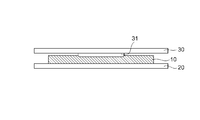
- a die is formed by using a press machine including a die 20 positioned on the lower side and a punch 30 positioned on the upper side and formed with a protruding portion 31 on the lower surface facing the die 20.
- the base material 10 on which the Sn—CuSn mixed layer is formed is disposed between the punch 20 and the punch 30 (first step).
- the punch 30 is pressed against the die 20 with a predetermined pressure while the substrate 10 is sandwiched between the die 20 and the punch 30. Crushing process (second step).
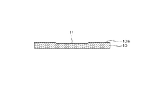
- the outermost surface 10 a of the base material 10 is formed with the concave portion 11 corresponding to the protruding portion 31 of the punch 30, and the outermost surface 10 a is crushed.
- a plurality of fine surface cracks are formed in the recess 11 (third step).
- the both ends in the longitudinal direction of the base material 10 are gripped with a predetermined jig, and a process of pulling by a predetermined amount (pulling process) is performed.
- the base material 10 in which the concave portion 11 is formed is disposed between the lower holding member 40 and the upper holding member 50 using a dimple processing machine provided with the upper holding member 50 (fourth step).
- the upper holding member 50 is fixed to the lower holding member 40 while the base member 10 is sandwiched between the lower holding member 40 and the upper holding member 50 in which the convex portions 41 are formed.
- dimple processing is performed on the concave portion 11 of the base material 10 from the back surface 10b side (fifth step).
- a hemispherical dimple 12 having a predetermined depth and a predetermined vertex curvature radius is formed with respect to the back surface 10b of the substrate 10.
- a dome-like shape having a predetermined height protruding upward from the recess 11 of the base material 10 and a vertex curvature radius larger than the dimple 12 is formed.
- a plurality of convex portions 13 are formed.
- the stroke in the depth direction of the punch 30 is further increased to cause surface cracks. It is sufficient to increase the number of.
- the number of surface cracks is not limited to this, and the number of surface cracks can be reduced by decreasing the vertex curvature radius of the convex portion 13 of the substrate 10 or by increasing only the height of the convex portion 13 while maintaining the vertex curvature radius. May be increased.
- the number of surface cracks can be increased according to the vertex curvature radius and height of the convex portion 13, as compared with the case where the number of surface cracks is adjusted by further increasing the crushing stroke for the base material 10.
- the contact pressure with the female terminal changes, which affects the reliability of electrical connection such as insertion / extraction force and fine sliding wear. It is desirable that the number of grooves can be controlled without changing the height of the convex portion 13.
- the contact area with the female terminal is changed, and the reliability of electrical connection such as fine sliding wear is affected. It is desirable to be able to control the number of grooves without changing the radius.
- the surface of the surface of the base material 10 is crushed by the convex portion 31 of the punch 30 and the crushing processing conditions are changed in advance. It is desirable to control the number of cracks.
- the base material used for the male terminal is a conductive copper alloy strip (plate material) having a thickness of 0.25 mm, a width of 40 mm or more, and a length of 100 mm or more. After molding to 20 mm, both ends in the width direction of the plate material are removed by 5 mm or more so as to have a width of 30 mm and cut to a length of 50 mm.
- plate material conductive copper alloy strip
- Pretreatment cathode electrolytic degreasing, pickling
- Ni intermediate layer plating Cu intermediate layer plating
- Sn outermost layer plating Sn outermost layer plating
- the cathode electrolytic degreasing conditions in the pretreatment were a degreasing solution: NaOH 60 g / liter, a degreasing condition: 2.5 A / dm 2, a temperature of 60 ° C., and a degreasing time of 60 seconds.
- the pickling conditions were pickling solution: 10% sulfuric acid, pickling condition: immersion for 30 seconds at room temperature (27 ° C.).
- Ni intermediate layer plating The condition for forming the Ni layer by Ni intermediate layer plating is an additive-free watt bath without using any additive, and plating solution: Ni (SO3NH2) 2 ⁇ 4H2O 500 g / liter, NiCl2 30 g / liter, H3BO3 30 g / Liter, plating conditions: temperature 50 ° C., current density 5 A / dm 2, Ni layer thickness: 0.5 ⁇ m.
- the conditions for forming the Cu layer by Cu intermediate layer plating are: plating solution: copper sulfate 180 g / liter, sulfuric acid 80 g / liter, plating condition: temperature 40 ° C., current density 5 A / dm 2, Cu layer thickness: 0.24 ⁇ m 0.26 ⁇ m, 0.40 ⁇ m, and 0.60 ⁇ m.
- the conditions for forming the Sn layer by Sn outermost layer plating are: plating solution: sulfuric acid Sn 80 g / liter, sulfuric acid 80 g / liter, plating condition: temperature 20 ° C., current density 5 A / dm 2, Sn layer (outermost layer) thickness : 0.6 ⁇ m, 0.58 ⁇ m, 0.50 ⁇ m, 0.3 ⁇ m.
- the CuSn layer is adjusted to have a desired exposed area ratio.
- the reflow process conditions were a reflow temperature of 300 ° C. and a reflow time of 10 seconds.
- the exposed area ratio of the CuSn layer with respect to the outermost surface of the Sn—CuSn mixed layer of the substrate 10 was adjusted to 5%, 15%, 50%, and 100%.
- the crushing processing conditions were such that the stroke amount of pressing the punch 30 into the base material 10 in the press machine was changed from 0 ⁇ m (no crushing) to 24 ⁇ m.
- the dimple processing conditions were all unified, and a vertex curvature radius of 1 mm of the final shape of the convex portion 13 of the base material 10 formed by dimple processing was obtained. Thereby, the number of grooves formed on the outermost surface of the Sn—CuSn mixed layer of the substrate 10 was controlled.
- the exposed area ratio of the Cu—Sn mixed layer was measured by image analysis.
- the exposed area ratio of the CuSn layer to the outermost surface of the Sn—CuSn mixed layer of the substrate 10 was calculated as a ratio (%) of the CuSn layer exposed to the outermost surface of the Sn—CuSn mixed layer. That is, when the CuSn layer and the Sn layer are half exposed with respect to the entire outermost surface of the Sn—CuSn mixed layer, the exposed area ratio of the CuSn layer is 50%.
- a total of six cross sections are observed, with three cross sections at predetermined intervals along the rolling parallel direction parallel to the rolling surface of the finish rolling on the base material 10.
- a SIM image of one cross section with respect to one convex portion 13 is used.
- the groove width W is 20 nm to 500 nm, for example, and the groove depth D is 0. 0 of the average thickness of the Sn—CuSn mixed layer.
- the number of grooves G1 of 0.3 ⁇ m to 0.9 ⁇ m corresponding to 5 times or more and less than 1.0 times is calculated. That is, the number of grooves G2 and G3 that do not satisfy this criterion and are not exposed on the outermost surface sf of the Sn—CuSn mixed layer is not subject to calculation.
- the unit length is a length of 100 ⁇ m along the outermost surface sf of the Sn—CuSn mixed layer in the cross section perpendicular to the rolling parallel direction with respect to the base material 10.
- the number n of grooves G1 where the groove width W and the groove depth D of the cross section satisfy the above-described numerical ranges is calculated. This is done for 6 cross sections. Then, after obtaining the number n of the grooves G1 per 1 ⁇ m, the number G1n of the grooves G1 per unit length of 100 ⁇ m was calculated by multiplying by 100.
- the number G1n can be expressed by the following equation (1).
- G1n (number n / length L (30 ⁇ m ⁇ 6)) ⁇ 100 (1)
- the dynamic friction coefficient between the convex portion 13 of the base material 10 in the male terminal and the female terminal as the counterpart was measured by a dynamic friction coefficient measuring device 60 shown in FIG.
- the dynamic friction coefficient measuring device 60 fixes the base material 10 to a horizontal base 62, and places a female test piece 63 corresponding to a female terminal on it to contact each other.
- the base material 10 is pressed from above the female test piece 63 by applying a load of 3.0 N with the weight 64, and using the horizontal load measuring device (Iko Engineering Co., Ltd .: Model-2152) 65, the base material 10 is pressed. Is pulled in the horizontal direction (in the direction of the arrow) (sliding speed 80 mm / min), and the maximum frictional force F (N) up to a sliding distance of 5 mm is measured.
- the contact resistance after the substrate 10 is heated and held at 100 ° C. for 120 hours is evaluated by a so-called four-terminal method.
- the value of the contact resistance is an index of heat resistance.
- the contact pressure of the probe is 2N and the energization current is 10 mA.
- a hemisphere having a curvature of 1 mm is used at the tip of the probe.
- the base material 10 was cut into a length of 50 mm ⁇ width of 20 ⁇ thickness of 0.25 mm, and a portion other than the peripheral end portion of 5 mm was used as a measurement target.
- the number of measurement points was 10 and each measurement point was spaced 2 mm or more from each other.
- the average value of the measured values at 10 measurement points was defined as contact resistance r.
- contact resistance r When the value of the contact resistance r is less than 10 m ⁇ , “Excellent heat resistance” is indicated by “ ⁇ ”, and when it is 10 m ⁇ or more, “Inferior heat resistance” is indicated by “X”.
- Dynamic friction coefficient ⁇ and contact resistance corresponding to the number G1n of grooves G1 when the exposed area ratio of the CuSn layer constituting the Sn—CuSn mixed layer of the substrate 10 is 5%, 15%, 50%, and 100% ⁇ is shown in Tables 1 to 4.
- Example 2 As shown in Table 2, when the exposed area ratio of the CuSn layer is 15% and the number G1n of the grooves G1 is 9.4 to 86.4 as in Example 1.9 to Example 1.12. The evaluation of the dynamic friction coefficient ⁇ was “Excellent”, and the evaluation of the contact resistance r was “Excellent”. Further, when the number G1n of the grooves G1 is 3.3 to 4.6 as in Example 1.7 and Example 1.8, the evaluation of the dynamic friction coefficient ⁇ is “ ⁇ ” and the contact resistance r The evaluation of was “Excellent”.
- the exposed area ratio of the CuSn layer is 15%, it is indicated that at least 3 or more and 112 or less G1n grooves G1 are required per unit length of 100 ⁇ m. More preferably, if the number of grooves G1 is 3 or more and 100 or less, it can be said that the evaluation of the dynamic friction coefficient ⁇ and the evaluation of the contact resistance r are excellent.
- the contact resistance r is excellent in evaluation.
- Example 1 As shown in Table 4, when the exposed area ratio of the CuSn layer is 100% and the number G1n of the grooves G1 is 10.9 to 98.9 as in Example 1.21 to Example 1.24, The evaluation of the dynamic friction coefficient ⁇ was “Excellent”, and the evaluation of the contact resistance r was “Excellent”. When the number G1n of the grooves G1 is 3.1 to 5.3 as in Example 1.19 and Example 1.20, the evaluation of the dynamic friction coefficient ⁇ is “ ⁇ ” and the contact resistance r is The evaluation was “Excellent” and excellent.
- the number G1n of the grooves G1 is preferably at least 3 and not more than 100 per unit length of 100 ⁇ m, and the exposed area ratio of the CuSn layer at that time Is preferably 5% to 100%, more preferably 15% to 100%.
- both end portions in the longitudinal direction of the base material 10 are gripped by a predetermined jig,
- the dynamic friction coefficient ⁇ and the contact resistance ⁇ in the case of performing a tensile process of pulling by the amount were examined.
- the strain due to the pulling process is 1% and the distance between the jigs holding the both side ends of the base material 10 is 50 mm, it is assumed that the base material 10 is stretched by 0.5 mm with the jig. .
- a method for calculating the groove width W as shown in FIG. 7, an average value of all detected groove widths W is used.
- the groove G1 is formed by causing the surface crack generated in the CuSn layer to start is described, but the present invention is not limited to this, and the CuSn layer is not limited to this.
- the groove G1 may be formed from a surface crack generated in the Sn layer.
- the NI layer is formed as an intermediate layer between the Sn—CuSn mixed layer and the base material 10 is described.
- One or more intermediate layers of alloy, cobalt, cobalt alloy, copper, and copper alloy may be formed.
Landscapes
- Chemical & Material Sciences (AREA)
- Engineering & Computer Science (AREA)
- Chemical Kinetics & Catalysis (AREA)
- Electrochemistry (AREA)
- Materials Engineering (AREA)
- Metallurgy (AREA)
- Organic Chemistry (AREA)
- Electroplating Methods And Accessories (AREA)
- Laminated Bodies (AREA)
Abstract
従来よりも更に摩擦抵抗が低く(低い挿抜力)、かつ、電気的接続の信頼性(低い接触抵抗)を維持し得る簡易に製造可能な端子を提供する。 導電性の基材(10)からなる端子であって、前記基材(10)の表面(10a)にスズおよび銅スズの混合物からなるスズ-銅スズ混合層(Sn-CuSn混合層)を有し、前記スズ-銅スズ混合層(Sn-CuSn混合層)の最表面(10a)には、溝(G1)を備え、前記溝(G1)は、前記最表面(10a)に沿った方向の長さ100μm当たり3個ないし100個形成されている。
Description
本発明は、端子に関し、特に、自動車および電子部品等に用いられる銅または銅合金製の基材からなり、接合時の挿抜力が低く、高温下における接触抵抗が低く安定性に優れた嵌合型端子に関する。
従来、銅(Cu)、銅合金などの導電体の母材(以下、これを単に「母材」という。)上にスズ(Sn)、スズ合金などのSnメッキ層を設けたメッキ材料は、母材の優れた導電性と強度、および、メッキ層の優れた電気接続性と耐食性とを備えた高性能導体材料として知られており、各種の端子やコネクタなどに広く用いられている。
ところで近年、電子制御化が進む中でコネクタが多極化したため、雄コネクタの端子群と雌コネクタの端子群を挿抜する際に多大な力が必要になり、特に、自動車のエンジンルーム内などの狭い空間では挿抜作業が困難であった。コネクタの多極化は、特に小型端子を配したコネクタにおいて求められており、具体的には、タブ幅にして1.0mmや0.64mmの小型端子に対して強く要求されている。
そこで、組み付け作業の負荷を低減するという観点から、多極化した端子において挿抜力を低減することが求められている。この挿抜力が高いと、組み付けを行う作業者の負荷が増大してしまうので、挿抜力を低減するための構造をコネクタに導入しなければならず、コスト増の要因となっていた。
この挿抜力を低減する方法として、端子間の接触圧を弱める方法があるが、この方法はSnメッキ層が軟質のため、端子の接触面にフレッティング現象が起きて端子間に導通不良が発生することがある。
ここで、フレッティング現象とは、振動や温度変化などの原因で端子の接触面間に起きる微振動により、端子表面の軟質のSnメッキ層が摩耗して酸化し、比抵抗(比電気抵抗)の大きい摩耗粉になる現象である。この摩耗粉が接触面間に介在すると、接続不良が起きる。そして、このフレッティング現象は、端子間の接触圧が低いほど起き易い。
そのため、接触圧を下げずに挿抜力を低減することが望ましい。すなわち、端子間の摩擦力を下げる方法が望ましい。また、自動車のエンジンルーム内などでは、高温環境であるため、低挿抜性だけでなく、高温環境下においても安定した電気接続性が保持されることが必要である。
ところで、Cu板条からなる母材(基材)の表面に、Cu-Sn合金被覆層とSn被覆層がこの順に形成されており、Cu-Sn合金被覆層の材料表面露出面積率が3~75%、平均の厚さが0.1~3.0μm、かつCu含有量が20~70at%であり、Sn被覆層の平均の厚さが0.2~5.0μmであることを特徴とする接続部品用導電材料が提案されている(例えば、特許文献1を参照。)。
この特許文献1の接続部品用導電材料によれば、Cu板条からなる母材表面にCu-Sn合金被覆層とSn被覆層を形成した接続部品用導電材料において、摩擦係数が低く(すなわち、低い挿抜力)、同時に電気的特性の信頼性(すなわち、低い接触抵抗)を維持することができる。
また、導電性基材上にSnメッキ層が形成された雄端子と雌端子からなり、雄端子および雌端子の一方の端子の他方の端子との接点部の表面に、長手方向に互いに離間した複数の溝または凹部が形成された嵌合型接続端子が提案されている(例えば、特許文献2を参照。)。この特許文献2の嵌合型接続端子によれば、微摺動摩耗(フレッティング現象)による電気抵抗値の上昇を安価かつ十分に抑制することができる。
ところで、特許文献1(表3等を参照。)には、雄端子と雌端子の両方が通常のSnメッキであった場合の摩擦係数は0.53~0.55であるのに対し、特許文献1の接続部品用導電材料を用いれば摩擦係数が0.24~033に低減することが記載されている。
しかしながら、コネクタの多極化の要求は高く、これまでよりも一段と摩擦係数の低い接点用材料が必要とされている。また、特許文献1では、雌端子にのみ特許文献1の接続部品用導電材料を用いた場合の摩擦係数については記載されていない。
また、一般的に低挿抜力が必要な端子の多くは、接触圧が2N~6N程度である。特許文献2の嵌合型接続端子のように、雌端子の半球状等の接点部の接触円の直径は50μm~150μm程度であり、雄端子の溝の幅が100μm程度である場合、接触円の当接する位置に応じて接触抵抗が高くなることがあった。
この点については、溝幅や溝間隔を小さくすることにより解決可能であると考えられるが、特許文献2に記載された方法(プレス加工、エッチング加工、放電加工、機械加工またはレーザー加工)によって溝幅を小さく形成しようとすると、製造コストが非常に高くなり量産品としては現実的ではなかった。
例えば、プレス加工であれば、所望の溝の形状と対応した凹凸を金型に予め施しておき、当該金型を用いて加工すれば幅の小さな溝を形成することができるが、凹凸の幅、間隔、深さを小さくすると、金型の価格が高価になるとともに金型の交換頻度も増加し、製造コストが飛躍的に増大してしまう。
また、それ以外の加工方法(エッチング加工、放電加工、機械加工またはレーザー加工)については、凹凸の幅、間隔、深さを小さくすると、高い加工精度が必要とされるので、設備コストが増大するだけでなく、加工時間についても増加するので、この場合も製造コストが増大してしまう。
本発明は、上記の課題に鑑みなされたものであり、その目的は、従来よりも更に摩擦抵抗が低く(低い挿抜力)、かつ、電気的接続の信頼性(低い接触抵抗)を維持し得る簡易に製造可能な端子を提供することである。
上記目的を達成するために、本発明の端子において、導電性の基材(10)からなる端子であって、前記基材(10)の表面(10a)にスズおよび銅スズの混合物からなるスズ-銅スズ混合層(Sn-CuSn混合層)を有し、前記スズ-銅スズ混合層(Sn-CuSn混合層)の最表面(10a)には、溝(G1)を備え、前記溝(G1)は、前記最表面(10a)に沿った方向の長さ100μm当たり3個ないし100個形成されていることを特徴とする。
本発明において、前記スズ-銅スズ混合層(Sn-CuSn混合層)の前記最表面(10a)に対する前記銅スズ(CnSn層)の露出面積率が15%乃至100%であることを特徴とする。
本発明において、前記溝(G1)は、前記スズ-銅スズ混合層(Sn-CuSn混合層)における前記銅スズ(CuSn層)の部分に形成されていることを特徴とする。
本発明において、前記スズ-銅スズ混合層(Sn-CuSn混合層)と前記基材(10)との間には中間層(NI層)が形成され、 前記中間層(NI層)は、ニッケル、ニッケル合金、コバルト、コバルト合金、銅、銅合金のうち何れか1層以上であることを特徴とする。
本発明において、前記溝は、その溝幅が20~500nmであることを特徴とする。
本発明によれば、従来よりも更に摩擦抵抗が低く(低い挿抜力)、かつ、電気的接続の信頼性(低い接触抵抗)を維持し得る簡易に製造可能な端子を実現することができる。
<実施の形態>
以下、本発明における実施の形態を図面に基づいて説明する。なお、以下に説明する実施の形態はあくまでも例示であり、本発明の範囲において、種々の形態をとり得る。
以下、本発明における実施の形態を図面に基づいて説明する。なお、以下に説明する実施の形態はあくまでも例示であり、本発明の範囲において、種々の形態をとり得る。
<端子の動摩擦抵抗が低下する原理>
本発明の端子として用いられる雄端子において、導電性を有する銅合金条の基材に施されたスズ-銅スズ混合層(以下、これを「Sn-CuSn混合層」ともいう。)の最表面に対しプレス加工により微小な表面クラックを形成した後、当該表面クラックを起点として亀裂を進展させることにより所望の溝幅および溝深さからなる溝を予め複数形成しておく。これにより、雄端子のSn-CuSn混合層の最表面に形成された複数の溝に対して、プレス加工時に使用したプレス加工油(以下、これを単に「プレス油」という。)の成分が貯留されることになる。
本発明の端子として用いられる雄端子において、導電性を有する銅合金条の基材に施されたスズ-銅スズ混合層(以下、これを「Sn-CuSn混合層」ともいう。)の最表面に対しプレス加工により微小な表面クラックを形成した後、当該表面クラックを起点として亀裂を進展させることにより所望の溝幅および溝深さからなる溝を予め複数形成しておく。これにより、雄端子のSn-CuSn混合層の最表面に形成された複数の溝に対して、プレス加工時に使用したプレス加工油(以下、これを単に「プレス油」という。)の成分が貯留されることになる。
ここで、プレス油の種類としては、以下に示すものがよい。例えば、分子式CnH2n+2で表される炭化水素であり、n=9~60が好ましい。具体例としては、ノナン、デカン、ウンデカン、ドデカン、テトラデカン、ペンタデカン、ヘキサデカン等が挙げられる。また、炭素原子数5~40のエーテル化合物が好ましい。エーテル化合物の具体例としては、ジプロピルエーテル、アリルフェニルエーテル、エチルイソブチルエーテル、エチレングリコールジフェニルエーテル、ペンタフェニルエーテル、アルキル(例えば、ノニル、エイコシルなど)、ジフェニルエーテル等のエーテル結合基および疎水基のみからなるエーテル化合物が挙げられる。また、これらが複数混合したものでもよい。
したがって、雌端子と、雄端子とが嵌合すると、メッキ最表面に形成された複数の溝から嵌合面に対してプレス油の成分が供給され続けるため、雌端子と雄端子との間の接点部分に対して効果的に潤滑作用が働き、雌端子と雄端子との動摩擦抵抗が低下する。なお、複数の溝を形成するのは、雄端子だけに限らず、雌端子のメッキ最表面に形成したり、或いは、雄端子および雌端子の双方に形成するようにしてもよい。
ここで、雄端子の基材上のSn-CuSn混合層に形成される溝は、通常、軟質のSn層ではなく、当該Sn層よりも硬質のCuSn層に形成される。これは、軟質のSn層よりも硬質のCuSn層の方がプレス加工時に生じた表面クラックが大きな亀裂へと進展し易いからである。ただし、溝は、CuSn層だけではなく、Sn層に形成できる場合には、当該Sn層の溝をプレス油の貯留に用いてもよい。
<溝の個数>
基材上のSn-CuSn混合層に形成された複数の溝の個数が所定の基準値よりも少な過ぎる場合は、摩擦係数が高くなる。これは、溝の個数が少ないためにプレス油の供給量が少なくなり、摩擦係数を低減させる効果を期待できないためである。
基材上のSn-CuSn混合層に形成された複数の溝の個数が所定の基準値よりも少な過ぎる場合は、摩擦係数が高くなる。これは、溝の個数が少ないためにプレス油の供給量が少なくなり、摩擦係数を低減させる効果を期待できないためである。
一方、基材上のSn-CuSn混合層に形成された複数の溝の個数が所定の基準値よりも多過ぎる場合は、摩擦係数は低くなるが、高温(例えば、140℃以上)で所定時間以上放置した後の接触抵抗が高くなる。これは、溝の個数が多過ぎる場合、基材との接触面積が低減するためSn-CuSn混合層が一部剥がれ易くなり、基材からSn-CuSn混合層のメッキ表面へCu元素が拡散し、メッキ表面に拡散したCu元素が酸化するためである。
ここで、溝の個数に対する所定の基準値とは、後述するように、Sn-CuSn混合層の最表面において発生する亀裂からなる溝と直交する任意の方向(以下、これを「メッキ表面方向」ともいう。)の単位長さ(例えば、100μm)当たりの溝の個数が例えば3個乃至100個を基準値とする。したがって、この場合、溝の個数が少な過ぎるのは、メッキ表面方向の長さ100μm当たり3個未満の場合であり、溝の個数が多過ぎるのは、メッキ表面方向の長さ100μm当たり100個を超える場合である。
<Sn-CuSn混合層におけるCuSn層の露出面積率>
Sn-CuSn混合層を構成するCuSn層およびSn層のうち、CuSn層の最表面に対する露出面積率については、15%乃至100%とする。CuSn層の露出面積率が15%以下の場合、Sn-CuSn混合層の最表面に複数の溝が形成されていた場合であっても動摩擦係数が高くなる。
Sn-CuSn混合層を構成するCuSn層およびSn層のうち、CuSn層の最表面に対する露出面積率については、15%乃至100%とする。CuSn層の露出面積率が15%以下の場合、Sn-CuSn混合層の最表面に複数の溝が形成されていた場合であっても動摩擦係数が高くなる。
これは、CuSn層よりも軟質のSn層の方がSn-CuSn混合層の最表面に多く露出しているため、雄端子と雌端子とを接触させた際にSn層が押し潰され、その瞬間に溝からプレス油が放出されてしまい、嵌合中にプレス油を供給する効果が失われて動摩擦係数を低減できなくなるからである。
<溝幅>
基材上のSn-CuSn混合層に形成された溝の溝幅は、基準の値よりも狭過ぎると貯留させるプレス油の量が少なくなり、動摩擦係数を低減する効果が期待できなくなる。また、溝の溝幅が基準の値よりも広過ぎると、Sn-CuSn混合層が基材から剥がれ易くなるために電気的接続の信頼性が落ちてしまう。
基材上のSn-CuSn混合層に形成された溝の溝幅は、基準の値よりも狭過ぎると貯留させるプレス油の量が少なくなり、動摩擦係数を低減する効果が期待できなくなる。また、溝の溝幅が基準の値よりも広過ぎると、Sn-CuSn混合層が基材から剥がれ易くなるために電気的接続の信頼性が落ちてしまう。
ここで、溝幅における基準の値とは、Sn-CuSn層における断面の溝幅が20nm~500nmである。したがって、溝の溝幅が、20nm未満の場合に狭過ぎるとされ、500nmを越える場合に広過ぎるとされる。
<溝深さ>
基材上のSn-CuSn混合層の最表面に形成された溝の溝深さは、浅すぎると当該溝に貯留させるプレス油の量が少なくなり、動摩擦係数を低減する効果が期待できなくなる。
基材上のSn-CuSn混合層の最表面に形成された溝の溝深さは、浅すぎると当該溝に貯留させるプレス油の量が少なくなり、動摩擦係数を低減する効果が期待できなくなる。
また、溝の溝深さが深過ぎる場合、すなわち、溝が基材まで到達している場合、例えば約140℃以上の高温環境下において、溝を介して基材のCu元素がメッキ表層に拡散し、そのCu元素が酸化して接触抵抗が増大してしまう。したがって、溝が基材まで到達してしまうと、溝が基材にまで到達していない場合よりも、接触抵抗が格段に大きくなってしまう。
したがって、溝の溝深さとしては、Sn-CuSn混合層のメッキ厚さの半分以上の深さであり、かつ、メッキ厚さ以下の深さであることが望ましい。具体的には、溝の溝深さは、スズ-銅スズ混合層のメッキ平均厚さの0.5倍以上であり、かつ、1.0倍未満の深さであればよい。
<ニッケル層の有無>
雄端子においては、基材とSn-CuSn混合層との間にニッケル層を形成しておくことが望ましい。これは、基材の上にニッケル層が形成された状態でSn-CuSn混合層の表面クラックから亀裂を進展させる場合、当該ニッケル層で亀裂の進展が停止されて、それ以上の深さにならないように溝の溝深さを制御できるからである。
雄端子においては、基材とSn-CuSn混合層との間にニッケル層を形成しておくことが望ましい。これは、基材の上にニッケル層が形成された状態でSn-CuSn混合層の表面クラックから亀裂を進展させる場合、当該ニッケル層で亀裂の進展が停止されて、それ以上の深さにならないように溝の溝深さを制御できるからである。
基材にニッケル層が形成されていない場合、亀裂の進展が進み易く、その結果、亀裂が基材に到達してしまうことを停止することができない。そのため、ニッケル層が形成された場合に比べて溝の溝深さを制御することが困難となる。
<溝の作製方法>
最初に、銅合金条からなる基材の上にNi層、Cu層、Sn層を順に形成した後、リフローすることによりスズと銅スズとが拡散したSn-CuSn混合層(スズ-銅スズ混合層)のメッキ最表層を形成する。ここで、Sn-CuSn混合層におけるCuSn層の最表面に対する露出面積率は、基材の上に形成するCu層のメッキ厚、および、Sn層のメッキ厚を調整することにより実現する。
最初に、銅合金条からなる基材の上にNi層、Cu層、Sn層を順に形成した後、リフローすることによりスズと銅スズとが拡散したSn-CuSn混合層(スズ-銅スズ混合層)のメッキ最表層を形成する。ここで、Sn-CuSn混合層におけるCuSn層の最表面に対する露出面積率は、基材の上に形成するCu層のメッキ厚、および、Sn層のメッキ厚を調整することにより実現する。
その後、図1に示すように、下側に位置するダイ20と、上側に位置するとともに当該ダイ20へ向かう下面に突出部31が形成されたパンチ30とを備えるプレス加工機を用いて、ダイ20とパンチ30との間に、Sn-CuSn混合層が形成された基材10を配置する(第1工程)。
続いて、図2に示すように、当該ダイ20と当該パンチ30との間に基材10を挟み付けながら当該パンチ30を当該ダイ20に所定の圧力で押し付けることにより当該基材材10に対して潰し加工を施す(第2工程)。
このとき、図3に示すように、基材10の最表面10aには、パンチ30の突出部31に対応した凹部11が形成されるとともに、当該最表面10aのうち、潰し加工が施された凹部11の部分には、微細な表面クラック(図示せず)が複数形成される(第3工程)。なお、潰し加工の後、基材10の長手方向における両側端部を所定の治具で掴み、所定の量だけ引っ張る加工(引っ張り加工)を施す。
その後、図4に示すように、半球状の複数の凸状部41が形成された下側保持部材40と、基材10の凹部11と対応する箇所に当該凹部11よりも大きな開口50hが形成された上側保持部材50とを備えるディンプル加工機を用い、下側保持部材40と上側保持部材50との間に、凹部11が形成された基材10を配置する(第4工程)。
図5に示すように、凸状部41が形成された下側保持部材40と上側保持部材50との間に基材10を挟み付けながら、上側保持部材50を下側保持部材40に所定の圧力で押し付けることにより、基材10の凹部11に裏面10b側からディンプル加工を施す(第5工程)。これにより、当該基材10の裏面10bに対して所定の深さ、および、所定の頂点曲率半径からなる半球状のディンプル12が形成される。
この結果、図6に示すように、ディンプル12が形成されると同時に、基材10の凹部11から上方に突出した所定の高さ、および、ディンプル12よりも大きな頂点曲率半径からなるドーム状の凸部13が複数形成される。
ここで、複数の凸部13が形成される前の基材10の最表面10aのうち凹部11の部分には表面クラックが既に発生しているため、凸部13が形成される際、表面クラックを起点として亀裂が進展し、所望の溝幅、所望の溝深さの亀裂からなる溝が形成されることになる。
なお、溝の個数を増やすには、第2工程において、パンチ30の突出部31を基材10に押し付けて潰し加工を施すときの当該パンチ30の深さ方向のストロークを更に長くして表面クラックの数を増大させればよい。しかしながら、これに限るものではなく、基材10の凸部13の頂点曲率半径を小さくしたり、或いは、頂点曲率半径をそのままで凸部13の高さだけを高くすることにより、表面クラックの数を増大させてもよい。
ただし、凸部13の頂点曲率半径や高さに応じて表面クラックの数を増やすことができるが、基材10に対する潰し加工のストロークを更に長くして表面クラックの数を調整する場合に比べて、表面クラックの数のばらつきが多く、溝の個数を制御し難い。
また、基材10の凸部13の高さを変更すると、雌端子との接触圧が変わり、挿抜力、および、微摺動摩耗性等の電気的接続の信頼性に影響が出るので、できるだけ、凸部13の高さを変更することなく溝の個数を制御できることが望ましい。
更に、凸部13を形成するためのディンプル加工の頂点曲率半径を変更すると、雌端子との接触面積が変わり、微摺動摩耗性等の電気的接続の信頼性に影響が出るので、頂点曲率半径を変更することなく溝の個数を制御できることが望ましい。
したがって、基材10の凹部11にディンプル加工を施す前に、パンチ30の凸部31により基材10のメッキ最表面10aに潰し加工を施し、その潰し加工の条件を変更することにより、予め表面クラックの数を制御することが望ましい。
<実施例>
<溝の作製条件>
次に、溝の作製条件について具体的に説明する。
<溝の作製条件>
次に、溝の作製条件について具体的に説明する。
<基材の条件>
雄端子に用いられる基材は、厚さ0.25mm、幅40mm以上、長さ100mm以上の導電性の銅合金条(板材)であり、その基材に対して仕上圧延を施して厚さ0.20mmに成型後、当該板材の幅方向の両端部を5mm以上除去して幅30mmとするとともに長さ50mmに切断する。
雄端子に用いられる基材は、厚さ0.25mm、幅40mm以上、長さ100mm以上の導電性の銅合金条(板材)であり、その基材に対して仕上圧延を施して厚さ0.20mmに成型後、当該板材の幅方向の両端部を5mm以上除去して幅30mmとするとともに長さ50mmに切断する。
その基材に対して、前処理(カソード電解脱脂、酸洗)、Ni中間層めっき、Cu中間層めっき、Sn最表層めっき、および、リフロー処理を順番に行った。
<前処理の条件>
前処理のうちカソード電解脱脂の条件としては、脱脂液:NaOH 60g/リットル、脱脂条件:2.5A/dm2、温度60℃、脱脂時間60秒、とした。酸洗の条件としては、酸洗液:10%硫酸、酸洗条件:室温(27℃)にて30秒浸漬、とした。
前処理のうちカソード電解脱脂の条件としては、脱脂液:NaOH 60g/リットル、脱脂条件:2.5A/dm2、温度60℃、脱脂時間60秒、とした。酸洗の条件としては、酸洗液:10%硫酸、酸洗条件:室温(27℃)にて30秒浸漬、とした。
<Ni中間層めっきの条件>
Ni中間層めっきによりNi層を形成する条件としては、添加剤を用いることのない添加剤フリーワット浴であり、メッキ液:Ni(SO3NH2)2・4H2O 500g/リットル、NiCl2 30g/リットル、H3BO3 30g/リットル、めっき条件:温度50℃、電流密度5A/dm2、Ni層の厚さ:0.5μm、とした。
Ni中間層めっきによりNi層を形成する条件としては、添加剤を用いることのない添加剤フリーワット浴であり、メッキ液:Ni(SO3NH2)2・4H2O 500g/リットル、NiCl2 30g/リットル、H3BO3 30g/リットル、めっき条件:温度50℃、電流密度5A/dm2、Ni層の厚さ:0.5μm、とした。
<Cu中間層めっきの条件>
Cu中間層めっきによりCu層を形成する条件としては、メッキ液:硫酸銅 180g/リットル、硫酸 80g/リットル、めっき条件:温度40℃、電流密度5A/dm2、Cu層の厚さ:0.24μm、0.26μm、0.40μm、0.60μmとした。
Cu中間層めっきによりCu層を形成する条件としては、メッキ液:硫酸銅 180g/リットル、硫酸 80g/リットル、めっき条件:温度40℃、電流密度5A/dm2、Cu層の厚さ:0.24μm、0.26μm、0.40μm、0.60μmとした。
<Sn最表層めっきの条件>
Sn最表層めっきによりSn層を形成する条件としては、メッキ液:硫酸Sn 80g/リットル、硫酸 80g/リットル、めっき条件:温度20℃、電流密度5A/dm2、Sn層(最表層)の厚さ:0.6μm、0.58μm、0.50μm、0.3μm、とした。ここで、CuSn層を所望の露出面積率となるように調整する。
Sn最表層めっきによりSn層を形成する条件としては、メッキ液:硫酸Sn 80g/リットル、硫酸 80g/リットル、めっき条件:温度20℃、電流密度5A/dm2、Sn層(最表層)の厚さ:0.6μm、0.58μm、0.50μm、0.3μm、とした。ここで、CuSn層を所望の露出面積率となるように調整する。
<リフロー処理の条件>
リフロー処理の条件としては、リフロー温度:300℃、リフロー時間:10秒とした。
リフロー処理の条件としては、リフロー温度:300℃、リフロー時間:10秒とした。
このような条件で上述した各種処理を行うことにより、基材10のSn-CuSn混合層の最表面に対するCuSn層の露出面積率を5%、15%、50%、100%に調整した。
<潰し加工およびディンプル加工の条件>
その後、CuSn層の露出面積率がそれぞれ異なる基材に対し、上述したように潰し加工(プレス加工)、ディンプル加工を順番に行った。
その後、CuSn層の露出面積率がそれぞれ異なる基材に対し、上述したように潰し加工(プレス加工)、ディンプル加工を順番に行った。
ここで、潰し加工条件は、プレス加工機におけるパンチ30の基材10に対する押し込みのストローク量を0μm(潰しなし)から24μmの間で変更した。ディンプル加工条件は、全て統一し、ディンプル加工により形成される基材10の凸部13の最終形状の頂点曲率半径1mmを得た。これにより、基材10のSn-CuSn混合層の最表面に形成する溝の個数を制御した。
<露出面積率の算出>
供試材の表面を、EDX( エネルギー分散型X 線分光分析器)を搭載したSEM( 走査型電子顕微鏡)を用いて200倍の倍率で観察し、得られた組成像の濃淡( 汚れや傷等のコントラストは除く)から画像解析によりCu-Sn混合層(Cu-Sn合金被覆層)の露出面積率を測定した。基材10のSn-CuSn混合層の最表面に対するCuSn層の露出面積率については、Sn-CuSn混合層の最表面に対して露出するCuSn層の割合(%)として算出した。すなわち、Sn-CuSn混合層の最表面の全体に対してCuSn層とSn層とが半分ずつ露出している場合、CuSn層の露出面積率は50%となる。
供試材の表面を、EDX( エネルギー分散型X 線分光分析器)を搭載したSEM( 走査型電子顕微鏡)を用いて200倍の倍率で観察し、得られた組成像の濃淡( 汚れや傷等のコントラストは除く)から画像解析によりCu-Sn混合層(Cu-Sn合金被覆層)の露出面積率を測定した。基材10のSn-CuSn混合層の最表面に対するCuSn層の露出面積率については、Sn-CuSn混合層の最表面に対して露出するCuSn層の割合(%)として算出した。すなわち、Sn-CuSn混合層の最表面の全体に対してCuSn層とSn層とが半分ずつ露出している場合、CuSn層の露出面積率は50%となる。
<溝の個数の算出>
基材10のSn-CuSn混合層の最表面に形成した複数の溝の個数を算出するには、微細加工用のFIB(Focused Ion Beam)装置により、当該基材10の凸部13の頂点を長さ30μm、深さ3~10μmの断面に削り出し、その断面を高倍率のSIM(Scanning Ion Microscope)像により観察する。
基材10のSn-CuSn混合層の最表面に形成した複数の溝の個数を算出するには、微細加工用のFIB(Focused Ion Beam)装置により、当該基材10の凸部13の頂点を長さ30μm、深さ3~10μmの断面に削り出し、その断面を高倍率のSIM(Scanning Ion Microscope)像により観察する。
断面の削り出しは、基材10に対する仕上圧延の圧延面と平行な圧延平行方向、に沿って所定間隔毎に3断面ずつ、合計6断面を観察する。なお、観察に当たっては、1つの凸部13に対して1断面のSIM像とする。
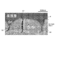
この場合、図7に示すように、単位長さ当たりに存在する溝G1乃至G3のうち、溝幅Wが例えば20nm~500nm、溝深さDがSn-CuSn混合層の平均厚さの0.5倍以上、1.0倍未満に相当する例えば0.3μm~0.9μmの溝G1の個数を算出する。すなわち、この基準を満たさず、Sn-CuSn混合層の最表面sfに露出していない溝G2、溝G3については個数の算出対象とはしない。
ここで、単位長さとは、基材10に対する圧延平行方向と直交する断面においてSn-CuSn混合層の最表面sfに沿った長さ100μmとする。具体的には、図8に示すように、1断面における長さL(30μm)の中で、断面の溝幅Wおよび溝深さDが上述した数値範囲を満たす溝G1の個数nを算出し、それを6断面分行う。そして、1μm当たりの溝G1の個数nを求めた後に、100を乗算することにより、単位長さ100μm当たりの溝G1の個数G1nを算出した。
個数G1nは、次の(1)式で表すことができる。
G1n=(個数n/長さL(30μm×6))×100……………(1)
G1n=(個数n/長さL(30μm×6))×100……………(1)
<動摩擦係数の測定>
雄端子における基材10の凸部13と相手方となる雌端子との動摩擦係数を、図9に示す動摩擦係数測定装置60により測定した。動摩擦係数測定装置60は、基材10を水平な台62に固定し、その上に雌端子に相当する雌試験片63を載置して互いに接触させる。
雄端子における基材10の凸部13と相手方となる雌端子との動摩擦係数を、図9に示す動摩擦係数測定装置60により測定した。動摩擦係数測定装置60は、基材10を水平な台62に固定し、その上に雌端子に相当する雌試験片63を載置して互いに接触させる。
続いて、雌試験片63の上から錘64により3.0Nの荷重をかけて基材10を押圧し、横型荷重測定器(アイコーエンジニアリング株式会社:Model-2152)65を用いて、基材10を水平方向(矢印方向)に引っ張り(摺動速度80mm/min)、摺動距離5mmまでの最大摩擦力F(N)を測定し、そのときの動摩擦係数μを次の(2)式により得た。
μ=F/3.0(N)……………………………………………………(2)
μ=F/3.0(N)……………………………………………………(2)
この動摩擦係数μの値が0.25よりも小さい場合、「摩擦力が小さい」として「○」、0.25以上の場合を「摩擦力が大きい」として「×」で示す。さらに、動摩擦係数μの値が0.20よりも小さい場合を「特に摩擦力が小さい」として「◎」として示す。
<高温加熱後の接触抵抗の測定>
基材10を100℃で120時間高温加熱して保持した後の接触抵抗を、いわゆる四端子法により評価する。この接触抵抗の値は、耐熱性の指標となる。プローブの接触圧を2N、通電電流10mAとする。プローブの先端には、曲率1mmの半球を用いる。この場合、基材10は、縦50mm×横20×厚さ0.25mmに切断したものであり、周囲の端部5mm以外の部分を測定対象として用いた。
基材10を100℃で120時間高温加熱して保持した後の接触抵抗を、いわゆる四端子法により評価する。この接触抵抗の値は、耐熱性の指標となる。プローブの接触圧を2N、通電電流10mAとする。プローブの先端には、曲率1mmの半球を用いる。この場合、基材10は、縦50mm×横20×厚さ0.25mmに切断したものであり、周囲の端部5mm以外の部分を測定対象として用いた。
測定箇所は、10箇所とし、それぞれの測定点は、互いに2mm以上の間隔を空けた。10箇所の測定点における測定値の平均値を接触抵抗rとした。接触抵抗rの値が10mΩ未満の場合を「耐熱性に優れる」として「○」、10mΩ以上の場合を「耐熱性に劣る」として「×」で示す。
<CuSn層の露出面積率および溝の個数に応じた動摩擦係数および接触抵抗>
基材10のSn-CuSn混合層を構成するCuSn層の最表面に対する露出面積率が5%、15%、50%、100%の場合における溝G1の個数G1nに応じた動摩擦係数μおよび接触抵抗μを表1乃至表4に示す。
基材10のSn-CuSn混合層を構成するCuSn層の最表面に対する露出面積率が5%、15%、50%、100%の場合における溝G1の個数G1nに応じた動摩擦係数μおよび接触抵抗μを表1乃至表4に示す。

表1に示すように、CuSn層の露出面積率が5%において、実施例1.1乃至実施例1.6のように溝G1の個数G1nが3.2個~7.2個の場合、動摩擦係数μおよび接触抵抗rの評価は何れも「○」であった。但し、比較例1.1乃至比較例1.4のように、溝G1の個数G1nが0.1個~1.6個の非常に少ない場合、接触抵抗rの評価は「○」であったが、動摩擦係数μの評価は全て「×」であった。すなわち、CuSn層の露出面積率が5%の場合、単位長さ100μm当たり少なくとも3個以上の溝G1が必要であることが示されている。
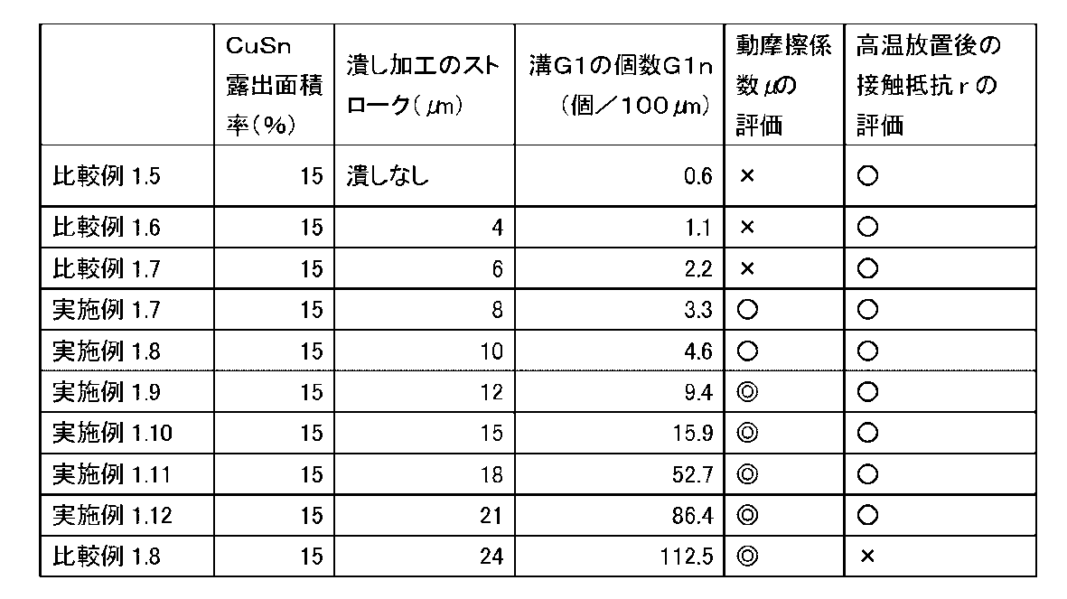
表2に示すように、CuSn層の露出面積率が15%において、実施例1.9乃至実施例1.12のように溝G1の個数G1nが9.4個~86.4個の場合、動摩擦係数μの評価は「◎」、および、接触抵抗rの評価は「○」で非常に優れていた。また、実施例1.7および実施例1.8のように、溝G1の個数G1nが3.3個~4.6個の場合、動摩擦係数μの評価は「○」、および、接触抵抗rの評価は「○」で優れていた。
但し、比較例1.5乃至比較例1.7のように、溝G1の個数G1nが0.6個~2.2個の非常に少ない場合、動摩擦係数μの評価は「×」であり、比較例1.8のように溝G1の個数G1nが112.5個の非常に多い場合、動摩擦係数μの評価は「◎」であったが、接触抵抗rの評価は「×」であった。
すなわち、CuSn層の露出面積率が15%の場合であっても、単位長さ100μm当たり少なくとも3個以上でかつ、112個以下の個数G1nの溝G1が必要であることが示されている。より好ましくは、3個以上でかつ、100個以下の個数G1nの溝G1であれば、動摩擦係数μの評価、および、接触抵抗rの評価に優れているといえる。
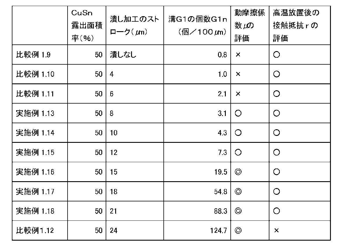
表3に示すように、CuSn層の露出面積率が50%において、実施例1.16乃至実施例1.18のように溝G1の個数G1nが19.5個~88.3個の場合、動摩擦係数μの評価は「◎」、および、接触抵抗rの評価は「○」で非常に優れていた。また、実施例1.13乃至実施例1.15のように、溝G1の個数G1nが3.1個~7.3個の場合、動摩擦係数μの評価は「○」、および、接触抵抗rの評価は「○」で優れていた。
但し、比較例1.9乃至比較例1.11のように、溝G1の個数G1nが0.8個~2.1個の非常に少ない場合、動摩擦係数μの評価は「×」であり、比較例1.12のように溝G1の個数G1nが124.7個の非常に多い場合、動摩擦係数μの評価は「◎」であったが、接触抵抗rの評価は「×」であった。
すなわち、CuSn層の露出面積率が50%の場合であっても、単位長さ100μm当たり少なくとも3個以上でかつ、88個以下の個数G1nの溝G1であれば、動摩擦係数μの評価、および、接触抵抗rの評価に優れているといえる。

表4に示すように、CuSn層の露出面積率が100%において、実施例1.21乃至実施例1.24のように溝G1の個数G1nが10.9個~98.9個の場合、動摩擦係数μの評価は「◎」、および、接触抵抗rの評価は「○」で非常に優れていた。また、実施例1.19および実施例1.20のように溝G1の個数G1nが3.1個~5.3個の場合、動摩擦係数μの評価は「○」、および、接触抵抗rの評価は「○」で優れていた。
但し、比較例1.13乃至比較例1.15のように、溝G1の個数G1nが1.1個~2.6個の非常に少ない場合、動摩擦係数μの評価は「×」であり、比較例1.16のように溝G1の個数G1nが122.9個の非常に多い場合、動摩擦係数μの評価は「◎」であったが、接触抵抗rの評価は「×」であった。
すなわち、CuSn層の露出面積率が100%の場合であっても、単位長さ100μm当たり少なくとも3個以上でかつ、98個以下の個数G1nの溝G1であれば、動摩擦係数μの評価、および、接触抵抗rの評価に優れているといえる。
このように、表1乃至表4によれば、溝G1の個数G1nは、単位長さ100μm当たり少なくとも3個以上で100個以下であることが望ましく、さらに、そのときのCuSn層の露出面積率は、5%ないし100%、より好ましくは、15%乃至100%であることが望ましい。

さらに、表5に示すように、潰し加工(第3工程)の後、ディンプル加工(第4工程)の前に、基材10の長手方向における両側端部を所定の治具で掴み、所定の量だけ引っ張るという引っ張り加工を施した場合の動摩擦係数μおよび接触抵抗μについて検討した。
この場合、例えば、引っ張り加工による歪が1%、基材10の両側端部を掴む治具間の距離が50mmの場合、治具により基材10を0.5mm引っ張って延ばすことを前提とする。なお、溝幅Wの算出方法としては、図7に示したように、検出された全ての溝幅Wの平均値とする。
表5では、実施例1.25乃至実施例1.28のように、溝幅Wが20nm~500nmの場合、動摩擦係数μおよび接触抵抗μは全て「○」で優れていた。ただし、比較例1.17のように溝幅Wが10nmの場合には、動摩擦係数μの評価は「×」であり、比較例1.18のように溝幅Wが1000nmの場合には、接触抵抗rの評価が「×」であった。
<他の実施の形態>
なお、上述した実施の形態においては、CuSn層に発生した表面クラックを起点に亀裂を進展させて溝G1を形成するようにした場合について述べたが、本発明はこれに限らず、CuSn層に加えてSn層に発生した表面クラックから溝G1を形成するようにしてもよい。
なお、上述した実施の形態においては、CuSn層に発生した表面クラックを起点に亀裂を進展させて溝G1を形成するようにした場合について述べたが、本発明はこれに限らず、CuSn層に加えてSn層に発生した表面クラックから溝G1を形成するようにしてもよい。
また、上述した実施の形態においては、Sn-CuSn混合層と基材10との間にはNI層を中間層として形成するようにした場合について述べてが、本発明はこれに限らず、ニッケル合金、コバルト、コバルト合金、銅、銅合金のうち何れか1層以上の中間層を形成するようにしてもよい。
10 基材
10a 最表面
10b 裏面
11 凹部
12 ディンプル
13 凸部
20 ダイ
30 パンチ
31 突出部
40 下側保持部材
41 凸状部
50h 開口
50 上側保持部材
60 動摩擦係数測定装置
62 台
63 雌試験片
64 錘
65 横型荷重測定器
10a 最表面
10b 裏面
11 凹部
12 ディンプル
13 凸部
20 ダイ
30 パンチ
31 突出部
40 下側保持部材
41 凸状部
50h 開口
50 上側保持部材
60 動摩擦係数測定装置
62 台
63 雌試験片
64 錘
65 横型荷重測定器
Claims (5)
- 導電性の基材からなる端子であって、
前記基材の表面にスズおよび銅スズの混合物からなるスズ-銅スズ混合層を有し、
前記スズ-銅スズ混合層の最表面には、溝を備え、
前記溝は、前記最表面に沿った方向の長さ100μm当たり3個ないし100個形成されている
ことを特徴とする端子。 - 前記スズ-銅スズ混合層の前記最表面に対する前記銅スズの露出面積率が15%乃至100%である
ことを特徴とする請求項1に記載の端子。 - 前記溝は、前記スズ-銅スズ混合層における前記銅スズの部分に形成されている
ことを特徴とする請求項1または2に記載の端子。 - 前記スズ-銅スズ混合層と前記基材との間には中間層が形成され、
前記中間層は、ニッケル、ニッケル合金、コバルト、コバルト合金、銅、銅合金のうち何れか1層以上である
ことを特徴とする請求項1乃至3何れか一項に記載の端子。 - 前記溝は、その溝幅が20~500nmである
ことを特徴とする請求項1乃至4何れか一項に記載の端子。
Priority Applications (1)
| Application Number | Priority Date | Filing Date | Title |
|---|---|---|---|
| JP2017536987A JP6647307B2 (ja) | 2016-03-29 | 2017-03-15 | 端子 |
Applications Claiming Priority (2)
| Application Number | Priority Date | Filing Date | Title |
|---|---|---|---|
| JP2016-065819 | 2016-03-29 | ||
| JP2016065819 | 2016-03-29 |
Publications (1)
| Publication Number | Publication Date |
|---|---|
| WO2017169765A1 true WO2017169765A1 (ja) | 2017-10-05 |
Family
ID=59965259
Family Applications (1)
| Application Number | Title | Priority Date | Filing Date |
|---|---|---|---|
| PCT/JP2017/010335 Ceased WO2017169765A1 (ja) | 2016-03-29 | 2017-03-15 | 端子 |
Country Status (2)
| Country | Link |
|---|---|
| JP (1) | JP6647307B2 (ja) |
| WO (1) | WO2017169765A1 (ja) |
Cited By (1)
| Publication number | Priority date | Publication date | Assignee | Title |
|---|---|---|---|---|
| US20210355595A1 (en) * | 2018-10-17 | 2021-11-18 | Kabushiki Kaisha Kobe Seiko Sho (Kobe Steel, Ltd.) | Copper or copper alloy sheet strip with surface coating layer |
Citations (3)
| Publication number | Priority date | Publication date | Assignee | Title |
|---|---|---|---|---|
| JP2008248294A (ja) * | 2007-03-29 | 2008-10-16 | Furukawa Electric Co Ltd:The | 潤滑性粒子を有するめっき材料、その製造方法およびそれを用いた電気・電子部品 |
| JP2009050904A (ja) * | 2007-08-29 | 2009-03-12 | Enshu Ltd | 周期構造体の加工制御方法と周期構造体の加工制御装置 |
| JP2010248616A (ja) * | 2009-03-26 | 2010-11-04 | Kobe Steel Ltd | 耐熱性に優れるSnめっき付き銅又は銅合金及びその製造方法 |
-
2017
- 2017-03-15 WO PCT/JP2017/010335 patent/WO2017169765A1/ja not_active Ceased
- 2017-03-15 JP JP2017536987A patent/JP6647307B2/ja active Active
Patent Citations (3)
| Publication number | Priority date | Publication date | Assignee | Title |
|---|---|---|---|---|
| JP2008248294A (ja) * | 2007-03-29 | 2008-10-16 | Furukawa Electric Co Ltd:The | 潤滑性粒子を有するめっき材料、その製造方法およびそれを用いた電気・電子部品 |
| JP2009050904A (ja) * | 2007-08-29 | 2009-03-12 | Enshu Ltd | 周期構造体の加工制御方法と周期構造体の加工制御装置 |
| JP2010248616A (ja) * | 2009-03-26 | 2010-11-04 | Kobe Steel Ltd | 耐熱性に優れるSnめっき付き銅又は銅合金及びその製造方法 |
Cited By (1)
| Publication number | Priority date | Publication date | Assignee | Title |
|---|---|---|---|---|
| US20210355595A1 (en) * | 2018-10-17 | 2021-11-18 | Kabushiki Kaisha Kobe Seiko Sho (Kobe Steel, Ltd.) | Copper or copper alloy sheet strip with surface coating layer |
Also Published As
| Publication number | Publication date |
|---|---|
| JPWO2017169765A1 (ja) | 2018-08-30 |
| JP6647307B2 (ja) | 2020-02-14 |
Similar Documents
| Publication | Publication Date | Title |
|---|---|---|
| KR102355331B1 (ko) | 주석 도금 구리 합금 단자재 및 그 제조 방법 | |
| JP6445895B2 (ja) | Snめっき材およびその製造方法 | |
| JP5263435B1 (ja) | 挿抜性に優れた錫めっき銅合金端子材 | |
| US20140004373A1 (en) | Tin-plated copper-alloy material for terminal and method for producing the same | |
| US20150184302A1 (en) | Tin-plated copper-alloy terminal material | |
| WO2009116602A1 (ja) | コネクタ用端子およびその製造方法 | |
| US20150056466A1 (en) | Tin-plated copper-alloy material for terminal having excellent insertion/extraction performance | |
| KR20140117274A (ko) | 삽입 발출성이 우수한 주석 도금 구리 합금 단자재 | |
| JP2014208904A (ja) | 耐摩耗性に優れる接続部品用導電材料 | |
| JP2014240520A (ja) | 挿抜性に優れた錫めっき銅合金端子材及びその製造方法 | |
| JP5089451B2 (ja) | コネクタ用金属材料およびその製造方法 | |
| KR102316967B1 (ko) | Sn 도금재 및 그의 제조 방법 | |
| JP5692799B2 (ja) | Snめっき材およびその製造方法 | |
| JP6647307B2 (ja) | 端子 | |
| JP5027013B2 (ja) | コネクタ用めっき角線材料 | |
| JP5415707B2 (ja) | コネクタ用金属材料およびその製造方法 | |
| JP6815876B2 (ja) | 嵌合型端子 | |
| JP2019071176A (ja) | 端子 | |
| JP7382702B2 (ja) | 端子 | |
| JP2013058418A (ja) | 接続端子およびその製造方法 | |
| JP5089452B2 (ja) | コネクタ用端子およびその製造方法 | |
| JP2023064183A (ja) | 電気接続部品用導電材料、ならびにこれを用いた接点、端子およびコネクタ | |
| JP2017043827A (ja) | Snめっき材およびその製造方法 | |
| JP2014005483A (ja) | 挿抜性に優れた錫めっき銅合金端子及び端子材 | |
| JP2009230931A (ja) | コネクタ用端子およびその製造方法 |
Legal Events
| Date | Code | Title | Description |
|---|---|---|---|
| ENP | Entry into the national phase |
Ref document number: 2017536987 Country of ref document: JP Kind code of ref document: A |
|
| NENP | Non-entry into the national phase |
Ref country code: DE |
|
| 121 | Ep: the epo has been informed by wipo that ep was designated in this application |
Ref document number: 17774309 Country of ref document: EP Kind code of ref document: A1 |
|
| 122 | Ep: pct application non-entry in european phase |
Ref document number: 17774309 Country of ref document: EP Kind code of ref document: A1 |