WO2017158465A1 - 記憶装置 - Google Patents
記憶装置 Download PDFInfo
- Publication number
- WO2017158465A1 WO2017158465A1 PCT/IB2017/051279 IB2017051279W WO2017158465A1 WO 2017158465 A1 WO2017158465 A1 WO 2017158465A1 IB 2017051279 W IB2017051279 W IB 2017051279W WO 2017158465 A1 WO2017158465 A1 WO 2017158465A1
- Authority
- WO
- WIPO (PCT)
- Prior art keywords
- transistor
- oxide semiconductor
- bit line
- circuit
- wiring
- Prior art date
- Legal status (The legal status is an assumption and is not a legal conclusion. Google has not performed a legal analysis and makes no representation as to the accuracy of the status listed.)
- Ceased
Links
Images













Classifications
-
- G—PHYSICS
- G11—INFORMATION STORAGE
- G11C—STATIC STORES
- G11C11/00—Digital stores characterised by the use of particular electric or magnetic storage elements; Storage elements therefor
- G11C11/21—Digital stores characterised by the use of particular electric or magnetic storage elements; Storage elements therefor using electric elements
- G11C11/34—Digital stores characterised by the use of particular electric or magnetic storage elements; Storage elements therefor using electric elements using semiconductor devices
- G11C11/40—Digital stores characterised by the use of particular electric or magnetic storage elements; Storage elements therefor using electric elements using semiconductor devices using transistors
- G11C11/41—Digital stores characterised by the use of particular electric or magnetic storage elements; Storage elements therefor using electric elements using semiconductor devices using transistors forming static cells with positive feedback, i.e. cells not needing refreshing or charge regeneration, e.g. bistable multivibrator or Schmitt trigger
- G11C11/412—Digital stores characterised by the use of particular electric or magnetic storage elements; Storage elements therefor using electric elements using semiconductor devices using transistors forming static cells with positive feedback, i.e. cells not needing refreshing or charge regeneration, e.g. bistable multivibrator or Schmitt trigger using field-effect transistors only
-
- G—PHYSICS
- G11—INFORMATION STORAGE
- G11C—STATIC STORES
- G11C11/00—Digital stores characterised by the use of particular electric or magnetic storage elements; Storage elements therefor
- G11C11/21—Digital stores characterised by the use of particular electric or magnetic storage elements; Storage elements therefor using electric elements
- G11C11/34—Digital stores characterised by the use of particular electric or magnetic storage elements; Storage elements therefor using electric elements using semiconductor devices
- G11C11/40—Digital stores characterised by the use of particular electric or magnetic storage elements; Storage elements therefor using electric elements using semiconductor devices using transistors
- G11C11/401—Digital stores characterised by the use of particular electric or magnetic storage elements; Storage elements therefor using electric elements using semiconductor devices using transistors forming cells needing refreshing or charge regeneration, i.e. dynamic cells
-
- G—PHYSICS
- G11—INFORMATION STORAGE
- G11C—STATIC STORES
- G11C14/00—Digital stores characterised by arrangements of cells having volatile and non-volatile storage properties for back-up when the power is down
- G11C14/0054—Digital stores characterised by arrangements of cells having volatile and non-volatile storage properties for back-up when the power is down in which the volatile element is a SRAM cell
-
- H—ELECTRICITY
- H10—SEMICONDUCTOR DEVICES; ELECTRIC SOLID-STATE DEVICES NOT OTHERWISE PROVIDED FOR
- H10B—ELECTRONIC MEMORY DEVICES
- H10B10/00—Static random access memory [SRAM] devices
- H10B10/12—Static random access memory [SRAM] devices comprising a MOSFET load element
-
- H—ELECTRICITY
- H10—SEMICONDUCTOR DEVICES; ELECTRIC SOLID-STATE DEVICES NOT OTHERWISE PROVIDED FOR
- H10D—INORGANIC ELECTRIC SEMICONDUCTOR DEVICES
- H10D30/00—Field-effect transistors [FET]
- H10D30/60—Insulated-gate field-effect transistors [IGFET]
- H10D30/67—Thin-film transistors [TFT]
- H10D30/6729—Thin-film transistors [TFT] characterised by the electrodes
- H10D30/673—Thin-film transistors [TFT] characterised by the electrodes characterised by the shapes, relative sizes or dispositions of the gate electrodes
- H10D30/6733—Multi-gate TFTs
- H10D30/6734—Multi-gate TFTs having gate electrodes arranged on both top and bottom sides of the channel, e.g. dual-gate TFTs
-
- H—ELECTRICITY
- H10—SEMICONDUCTOR DEVICES; ELECTRIC SOLID-STATE DEVICES NOT OTHERWISE PROVIDED FOR
- H10D—INORGANIC ELECTRIC SEMICONDUCTOR DEVICES
- H10D30/00—Field-effect transistors [FET]
- H10D30/60—Insulated-gate field-effect transistors [IGFET]
- H10D30/67—Thin-film transistors [TFT]
- H10D30/674—Thin-film transistors [TFT] characterised by the active materials
- H10D30/6755—Oxide semiconductors, e.g. zinc oxide, copper aluminium oxide or cadmium stannate
-
- H—ELECTRICITY
- H10—SEMICONDUCTOR DEVICES; ELECTRIC SOLID-STATE DEVICES NOT OTHERWISE PROVIDED FOR
- H10D—INORGANIC ELECTRIC SEMICONDUCTOR DEVICES
- H10D30/00—Field-effect transistors [FET]
- H10D30/60—Insulated-gate field-effect transistors [IGFET]
- H10D30/67—Thin-film transistors [TFT]
- H10D30/6757—Thin-film transistors [TFT] characterised by the structure of the channel, e.g. transverse or longitudinal shape or doping profile
-
- H—ELECTRICITY
- H10—SEMICONDUCTOR DEVICES; ELECTRIC SOLID-STATE DEVICES NOT OTHERWISE PROVIDED FOR
- H10D—INORGANIC ELECTRIC SEMICONDUCTOR DEVICES
- H10D30/00—Field-effect transistors [FET]
- H10D30/60—Insulated-gate field-effect transistors [IGFET]
- H10D30/69—IGFETs having charge trapping gate insulators, e.g. MNOS transistors
-
- H—ELECTRICITY
- H10—SEMICONDUCTOR DEVICES; ELECTRIC SOLID-STATE DEVICES NOT OTHERWISE PROVIDED FOR
- H10D—INORGANIC ELECTRIC SEMICONDUCTOR DEVICES
- H10D86/00—Integrated devices formed in or on insulating or conducting substrates, e.g. formed in silicon-on-insulator [SOI] substrates or on stainless steel or glass substrates
- H10D86/40—Integrated devices formed in or on insulating or conducting substrates, e.g. formed in silicon-on-insulator [SOI] substrates or on stainless steel or glass substrates characterised by multiple TFTs
- H10D86/421—Integrated devices formed in or on insulating or conducting substrates, e.g. formed in silicon-on-insulator [SOI] substrates or on stainless steel or glass substrates characterised by multiple TFTs having a particular composition, shape or crystalline structure of the active layer
- H10D86/423—Integrated devices formed in or on insulating or conducting substrates, e.g. formed in silicon-on-insulator [SOI] substrates or on stainless steel or glass substrates characterised by multiple TFTs having a particular composition, shape or crystalline structure of the active layer comprising semiconductor materials not belonging to the Group IV, e.g. InGaZnO
-
- H—ELECTRICITY
- H10—SEMICONDUCTOR DEVICES; ELECTRIC SOLID-STATE DEVICES NOT OTHERWISE PROVIDED FOR
- H10D—INORGANIC ELECTRIC SEMICONDUCTOR DEVICES
- H10D86/00—Integrated devices formed in or on insulating or conducting substrates, e.g. formed in silicon-on-insulator [SOI] substrates or on stainless steel or glass substrates
- H10D86/40—Integrated devices formed in or on insulating or conducting substrates, e.g. formed in silicon-on-insulator [SOI] substrates or on stainless steel or glass substrates characterised by multiple TFTs
- H10D86/60—Integrated devices formed in or on insulating or conducting substrates, e.g. formed in silicon-on-insulator [SOI] substrates or on stainless steel or glass substrates characterised by multiple TFTs wherein the TFTs are in active matrices
-
- H—ELECTRICITY
- H10—SEMICONDUCTOR DEVICES; ELECTRIC SOLID-STATE DEVICES NOT OTHERWISE PROVIDED FOR
- H10D—INORGANIC ELECTRIC SEMICONDUCTOR DEVICES
- H10D87/00—Integrated devices comprising both bulk components and either SOI or SOS components on the same substrate
-
- G—PHYSICS
- G11—INFORMATION STORAGE
- G11C—STATIC STORES
- G11C11/00—Digital stores characterised by the use of particular electric or magnetic storage elements; Storage elements therefor
- G11C11/21—Digital stores characterised by the use of particular electric or magnetic storage elements; Storage elements therefor using electric elements
- G11C11/34—Digital stores characterised by the use of particular electric or magnetic storage elements; Storage elements therefor using electric elements using semiconductor devices
- G11C11/40—Digital stores characterised by the use of particular electric or magnetic storage elements; Storage elements therefor using electric elements using semiconductor devices using transistors
- G11C11/401—Digital stores characterised by the use of particular electric or magnetic storage elements; Storage elements therefor using electric elements using semiconductor devices using transistors forming cells needing refreshing or charge regeneration, i.e. dynamic cells
- G11C11/403—Digital stores characterised by the use of particular electric or magnetic storage elements; Storage elements therefor using electric elements using semiconductor devices using transistors forming cells needing refreshing or charge regeneration, i.e. dynamic cells with charge regeneration common to a multiplicity of memory cells, i.e. external refresh
- G11C11/404—Digital stores characterised by the use of particular electric or magnetic storage elements; Storage elements therefor using electric elements using semiconductor devices using transistors forming cells needing refreshing or charge regeneration, i.e. dynamic cells with charge regeneration common to a multiplicity of memory cells, i.e. external refresh with one charge-transfer gate, e.g. MOS transistor, per cell
-
- G—PHYSICS
- G11—INFORMATION STORAGE
- G11C—STATIC STORES
- G11C11/00—Digital stores characterised by the use of particular electric or magnetic storage elements; Storage elements therefor
- G11C11/21—Digital stores characterised by the use of particular electric or magnetic storage elements; Storage elements therefor using electric elements
- G11C11/34—Digital stores characterised by the use of particular electric or magnetic storage elements; Storage elements therefor using electric elements using semiconductor devices
- G11C11/40—Digital stores characterised by the use of particular electric or magnetic storage elements; Storage elements therefor using electric elements using semiconductor devices using transistors
- G11C11/41—Digital stores characterised by the use of particular electric or magnetic storage elements; Storage elements therefor using electric elements using semiconductor devices using transistors forming static cells with positive feedback, i.e. cells not needing refreshing or charge regeneration, e.g. bistable multivibrator or Schmitt trigger
- G11C11/413—Auxiliary circuits, e.g. for addressing, decoding, driving, writing, sensing, timing or power reduction
- G11C11/417—Auxiliary circuits, e.g. for addressing, decoding, driving, writing, sensing, timing or power reduction for memory cells of the field-effect type
- G11C11/419—Read-write [R-W] circuits
Definitions
- One embodiment of the present invention relates to a semiconductor device, particularly a memory device.
- One embodiment of the present invention also relates to an object, a method, or a manufacturing method.
- one embodiment of the present invention relates to a process, a machine, a manufacture, or a composition (composition of matter).
- One embodiment of the present invention relates to a driving method or a manufacturing method thereof.
- a semiconductor device refers to all devices that can function by utilizing semiconductor characteristics.
- a memory device, a display device, an electro-optical device, a power storage device, a semiconductor circuit, and an electronic device may include a semiconductor device.
- the power consumption of an IC can be roughly divided into two: power consumption during operation (dynamic power) and power consumption when not operating (standby) (static power).
- dynamic power When the operating frequency is increased for higher performance, dynamic power increases.
- static power Most of the static power is the power consumed by the transistor leakage current.
- the leakage current includes sub-threshold leakage current, gate tunnel leakage current, gate-induced drain leakage (GIDL) current, and junction tunnel leakage current. Since these leakage currents increase with the miniaturization of transistors, an increase in power consumption is a major barrier to high performance and high integration of ICs.
- a circuit that does not need to be operated is stopped by power gating or clock gating.
- power gating the power supply is stopped, so there is an effect of eliminating standby power.
- Non-Patent Document 1 discloses an OS-SRAM (Static Random Access Memory) including a backup circuit using an OS transistor.
- Non-Patent Document 1 discloses that a microprocessor equipped with an OS-SRAM can perform power gating with a short break-even time (BET) without affecting normal operation.
- BET short break-even time
- the SRAM is a memory that operates at high speed, it is used for a data memory or a cache memory built in a logical circuit such as a CPU.
- low-voltage operation, standby current (non-access current), cell size, and the like become problems as the capacity of the SRAM increases.
- An object of one embodiment of the present invention is to provide a memory device with low power consumption. Another object of one embodiment of the present invention is to provide a memory device with a small circuit area. An object of one embodiment of the present invention is to provide a semiconductor device with low power consumption. Another object of one embodiment of the present invention is to provide a semiconductor device with a small circuit area. Another object of one embodiment of the present invention is to provide a novel semiconductor device.
- a plurality of memory cells a precharge circuit, a latch circuit, a bit line pair including a first bit line and a second bit line, a first local bit line, and a second local bit line
- a storage device having a local bit line pair, a first transistor, and a second transistor.
- the first transistor has a function of controlling a conduction state between the first bit line and the first local bit line.
- the second transistor has a function of controlling a conduction state between the second bit line and the second local bit line.
- Each of the plurality of memory cells includes a third transistor, a fourth transistor, a first capacitor element, and a second capacitor element.
- the third transistor has a function of controlling the conduction state between the first local bit line and the first capacitor element.
- the fourth transistor has a function of controlling the conduction state between the second local bit line and the second capacitor element.
- the precharge circuit has a function of supplying a precharge voltage to the local bit line pair.
- the latch circuit is electrically connected to the local bit line pair. The latch circuit is preferably supplied with the precharge voltage and one of the low power supply voltage and the high power supply voltage when the first transistor, the second transistor, the third transistor, and the fourth transistor are non-conductive.
- the third transistor preferably includes an oxide semiconductor in a channel formation region
- the fourth transistor preferably includes an oxide semiconductor in a channel formation region
- the plurality of memory cells are preferably provided on the precharge circuit or the latch circuit.
- a plurality of memory cells a precharge circuit, a latch circuit, a bit line pair including a first bit line and a second bit line, a first local bit line, and a second local bit line
- a storage device having a local bit line pair, a first transistor, and a second transistor.
- the first transistor has a function of controlling a conduction state between the first bit line and the first local bit line.
- the second transistor has a function of controlling a conduction state between the second bit line and the second local bit line.
- Each of the plurality of memory cells is classified as a first memory cell or a second memory cell.
- Each first memory cell has a third transistor and a first capacitor.
- Each second memory cell has a fourth transistor and a second capacitor.
- the third transistor has a function of controlling the conduction state between the first local bit line and the first capacitor element.
- the fourth transistor has a function of controlling the conduction state between the second local bit line and the second capacitor element.
- the precharge circuit has a function of supplying a precharge voltage to the local bit line pair.
- the latch circuit is electrically connected to the local bit line pair. The latch circuit is preferably supplied with the precharge voltage and one of the low power supply voltage and the high power supply voltage when the first transistor, the second transistor, the third transistor, and the fourth transistor are non-conductive.
- the third transistor preferably includes an oxide semiconductor in a channel formation region
- the fourth transistor preferably includes an oxide semiconductor in a channel formation region
- the plurality of memory cells are preferably provided on the precharge circuit or the latch circuit.
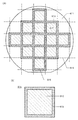
- One embodiment of the present invention is a semiconductor wafer including a plurality of the memory devices described in the above embodiments and having an isolation region.
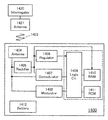
- One embodiment of the present invention is an electronic device including the storage device described in the above embodiment and a battery.
- a memory device with reduced power consumption can be provided.
- a memory device with a small circuit area can be provided.
- a semiconductor device with reduced power consumption can be provided.
- a semiconductor device with a small circuit area can be provided.
- One embodiment of the present invention can provide a novel semiconductor device.
- FIG. 1 is a block diagram illustrating a configuration example of a storage device.
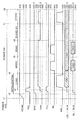
- the circuit diagram which shows the structural example of a memory cell. 4 is a timing chart illustrating an operation example of a storage device.
- FIG. 3 is a block diagram illustrating a structure example of a memory cell array.
- the circuit diagram which shows the structural example of a memory cell. The circuit diagram which shows the structural example of a memory cell.
- the circuit diagram which shows the structural example of a memory cell. The circuit diagram which shows a memory cell, a voltage holding circuit, and a voltage generation circuit.
- FIG. 1 is a block diagram illustrating a configuration example of a storage device.
- the circuit diagram which shows the structural example of a memory cell. 4 is a timing chart illustrating an operation
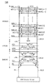
- FIG. 6 is a cross-sectional view illustrating a structure example of a memory device.
- FIG. 6 is a cross-sectional view illustrating a structure example of a memory device.
- FIG. 10 is a cross-sectional view illustrating a structural example of a transistor.
- FIG. 6 illustrates a crystal of InMZnO 4 .
- 4A and 4B are a top view and cross-sectional views illustrating a structural example of a transistor.
- 4A and 4B are a top view and cross-sectional views illustrating a structural example of a transistor.
- 4A and 4B are a top view and cross-sectional views illustrating a structural example of a transistor.
- 4A and 4B are a top view and cross-sectional views illustrating a structural example of a transistor.
- 4A and 4B are a top view and cross-sectional views illustrating a structural example of a transistor.
- the top view of a semiconductor wafer. 10A and 10B are a flowchart and a perspective view illustrating a manufacturing process of a semiconductor device.
- on-state current refers to drain current when a transistor is in an on state.
- the ON state is a state where the voltage between the gate and the source (V G ) is equal to or higher than the threshold voltage (V th ) in an n-channel transistor, and V G in a p-channel transistor unless otherwise specified. It means a state below Vth .
- the on-current of the n-channel transistor, V G refers to a drain current when the above V th.
- the on-state current of the transistor may depend on a voltage (V D ) between the drain and the source.
- off-state current refers to drain current when a transistor is off.
- the OFF state unless otherwise specified, the n-channel type transistor, V G is lower than V th states, in p-channel type transistor, V G means a state higher than V th.
- the off-current of the n-channel transistor refers to the drain current when V G is lower than V th.
- Off-state current of the transistor may be dependent on the V G. Accordingly, the off current of the transistor is less than 10 -21 A, and may refer to the value of V G to off-current of the transistor is less than 10 -21 A are present.
- the off-state current of the transistor may depend on V D.
- the off-state current is such that the absolute value of V D is 0.1 V, 0.8 V, 1 V, 1.2 V, 1.8 V, 2.5 V, 3 V, 3.3 V, 10 V , 12V, 16V, or 20V may be represented.
- the off-state current in V D used in a semiconductor device or the like including the transistor may be represented.
- one of a source and a drain is referred to as “one of a source and a drain” (or a first electrode or a first terminal), and the source and the drain The other is referred to as “the other of the source and the drain” (or the second electrode or the second terminal).
- the source and drain of a transistor vary depending on the structure or operating conditions of the transistor.
- the names of the source and the drain of the transistor can be appropriately rephrased depending on the situation, such as a source (drain) terminal or a source (drain) electrode.
- a high power supply voltage may be referred to as an H level (or V DD ), and a low power supply voltage may be referred to as an L level (or GND).
- the storage device of this embodiment includes a memory portion A that is nonvolatile but capable of high-speed processing and a memory portion B that can hold data for a long time even when the power is off.
- the memory unit A corresponds to a working memory, and exchanges data between the host device and the storage device.
- the memory unit B corresponds to a storage unit for long-term storage, and holds information written in the memory unit A for a long time.
- the memory unit B is slower in processing speed than the memory unit A, but has a larger capacity than the memory unit A.
- the memory unit B can hold data for a long time in a power-off state.
- FIG. 1 is a block diagram illustrating a configuration example of a storage device.
- a memory device 100 illustrated in FIG. 1 includes a memory cell array 110, a peripheral circuit 111, a control circuit 112, a voltage generation circuit 127, and power switches (PSW) 141 and 142.
- PSW power switches
- each circuit, each signal, and each voltage can be appropriately discarded as necessary.
- other circuits or other signals may be added.
- Signals BW, CE, GW, CLK, WAKE, ADDR, WDA, PON1, and PON2 are external input signals
- signal RDA is an external output signal.
- the signal CLK is a clock signal.
- Signals CE and GW and signal BW are control signals.
- the signal CE is a chip enable signal
- the signal GW is a global write enable signal
- the signal BW is a byte write enable signal.
- the signal ADDR is an address signal.
- the signal WDA is write data
- the signal RDA is read data.
- Signals PON1 and PON2 are power gating control signals.
- the signals PON1 and PON2 may be generated by the control circuit 112.
- the control circuit 112 is a logic circuit having a function of controlling the overall operation of the storage device 100. For example, the control circuit performs a logical operation on the signal CE, the signal GW, and the signal BW to determine an operation mode (for example, a write operation or a read operation) of the storage device 100. Alternatively, the control circuit 112 generates a control signal for the peripheral circuit 111 so that this operation mode is executed.
- the memory cell array 110 includes a plurality of memory cells (MC) 130 and a plurality of wirings WL, NWL, BL, and BLB.
- the plurality of memory cells 130 are arranged in a matrix.
- the memory cells 130 in the same row are electrically connected to the wirings WL and NWL in that row.
- the wirings WL and NWL are each word lines, and the wirings BL and BLB are bit line pairs for transmitting complementary data.
- the wiring BLB is a bit line to which data obtained by inverting the logic of BL is input, and is sometimes referred to as a bit complement line or an inverted bit line.
- the memory cell 130 has two types of memory circuits 10 and 20.
- the memory circuit 10 (hereinafter referred to as “SMC10”) is a memory circuit capable of storing 1-bit complementary data.
- the memory circuit 20 (hereinafter referred to as “NVM 20”) is a memory circuit capable of storing n-bit (n is an integer larger than 1) complementary data, and retains data for a long time even in a power-off state. It is possible. That is, the SMC 10 is a memory cell constituting the above-described memory unit A (working memory), and the NVM 20 is a memory cell constituting the above-described memory unit B (long-term storage storage unit).
- the voltage generation circuit 127 has a function of generating a negative voltage (V BG ).
- V BG is applied to a transistor used in the NVM 20.
- WAKE has a function of controlling the input of CLK to the voltage generation circuit 127. For example, when an H level signal is supplied to WAKE, the signal CLK is input to the voltage generation circuit 127, and the voltage generation circuit 127 generates VBG .
- the details of the voltage generation circuit 127 will be described with reference to FIGS.
- the SMC 10 and NVM 20 are electrically connected by a local bit line pair (wirings LBL, LBLB).
- the wiring LBLB is a local bit line for the wiring BL
- the wiring LBLB is a local bit line for the wiring BLB.
- the SMC 10 and the NVM 20 are electrically connected by the wirings LBL and LBLB.
- the memory cell 130 includes a circuit 30 (hereinafter referred to as “LPC 30”).
- the LPC 30 is a local precharge circuit for precharging the wiring LBL and the wiring LBLB.
- a control signal for the LPC 30 is generated by the peripheral circuit 111.
- the peripheral circuit 111 is a circuit for writing and reading data to and from the memory cell array 110.
- the peripheral circuit 111 has a function of driving the wirings WL, NWL, BL, and BLB.
- the peripheral circuit 111 includes a row decoder 121, a column decoder 122, a row driver 123, a column driver 124, an input circuit 125, and an output circuit 126.
- the row decoder 121 and the column decoder 122 have a function of decoding the signal ADDR.
- the row decoder 121 is a circuit for designating a row to be accessed
- the column decoder 122 is a circuit for designating a column to be accessed.
- the row driver 123 has a function of selecting the wirings WL and NWL in the row designated by the row decoder 121. Specifically, the row driver 123 has a function of generating a signal for selecting the wirings WL and NWL.
- the column driver 124 has a function of writing data into the memory cell array 110, a function of reading data from the memory cell array 110, a function of holding the read data, a function of precharging the wiring BL and the wiring BLB, and the like.
- the input circuit 125 has a function of holding the signal WDA. Data held by the input circuit 125 is output to the column driver 124. The output data of the input circuit 125 is data to be written in the memory cell array 110. Data (Dout) read from the memory cell array 110 by the column driver 124 is output to the output circuit 126. The output circuit 126 has a function of holding Dout. The output circuit 126 outputs the held data to the outside of the storage device 100. The output data is the signal RDA.
- the PSW 141 has a function of controlling the supply of VDD to circuits (peripheral circuits 115) other than the memory cell array 110.
- the PSW 142 has a function of controlling the supply of VHM to the row driver 123.
- the high power supply voltage of the storage device 100 is VDD
- the low power supply voltage is GND (ground potential).
- VHM is a high power supply voltage used for setting the wiring NWL to a high level, and is higher than VDD.
- On / off of the PSW 141 is controlled by the signal PON1, and on / off of the PSW 142 is controlled by the signal PON2.
- the number of power supply domains to which VDD is supplied is 1, but a plurality of power supply domains may be provided. In this case, a power switch may be provided for each power domain.
- FIG. 2 shows a circuit configuration example of the memory cell 130.
- the SMC 10 is electrically connected to the wiring BL, the wiring BLB, the wiring LBL, the wiring LBLB, the wiring VHH, and the wiring VLL.
- the SMC 10 has a circuit configuration similar to that of a CMOS type (6-transistor type) SRAM cell, and includes transistors Tld1, Tld2, Tdr1, Tdr2, Tac1, and Tac2.
- the transistors Tld1 and Tld2 are load transistors (pull-up transistors), the transistors Tdr1 and Tdr2 are drive transistors (pull-down transistors), and the transistors Tac1 and Tac2 are access transistors (transfer transistors).
- a conduction state between the wiring BL and the wiring LBL is controlled by the transistor Tac1.
- the conduction state between the wiring BLB and the wiring LBLB is controlled by the transistor Tac2.
- On / off of the transistors Tac1 and Tac2 is controlled by the potential of the wiring WL.
- An inverter is configured by the transistors Tld1 and Tdr1, and an inverter is configured by the transistors Tld2 and Tdr2.
- the input terminals of these two inverters are each electrically connected to the other output terminal, and a latch circuit is configured.
- a power supply voltage is supplied to the two inverters by wirings VHH and VLL.
- the NVM 20 shown in FIG. 2 has n (n is an integer of 1 or more) NMCs.
- the n NMCs are electrically connected to different wirings NWL.
- the n NMCs are electrically connected to one wiring VCS.
- symbols such as [0] and [1] are used, and in order to distinguish n wirings NWL, symbols such as _0 and _1 are used.
- the NMC is a memory circuit (also referred to as a memory cell) that can hold 1-bit complementary data.
- NMC has MC1 and MC2.
- MC1 is a memory cell for holding data written in the wiring LBL
- MC2 is a memory cell for holding data written in the wiring LBLB.
- MC1 and MC2 have the same circuit configuration as that of a memory cell of a one-transistor one-capacity dynamic random access memory (DRAM).
- MC1 includes a transistor Tr1 and a capacitor C1.
- MC2 includes a transistor Tr2 and a capacitor C2.
- the capacitive element C1 functions as a storage capacitor of MC1, and the capacitive element C2 functions as a storage capacitor of MC2.
- the wiring VCS is a power supply line for the storage capacitors of MC1 and MC2, and GND is input here.
- Gates (first gates) of the transistors Tr1 and Tr2 are each electrically connected to the wiring NWL.
- One of a source and a drain of the transistor Tr1 is electrically connected to the wiring LBL, and one of a source and a drain of the transistor Tr2 is electrically connected to the wiring LBLB.
- the first terminal of the capacitor C1 is electrically connected to the other of the source and the drain of the transistor Tr1, and the second terminal of the capacitor C1 is electrically connected to the VCS.
- the first terminal of the capacitor C2 is electrically connected to the other of the source and the drain of the transistor Tr2, and the second terminal is electrically connected to the VCS.
- the transistors Tr1 and Tr2 each have a second gate.
- the second gates of the transistors Tr1 and Tr2 are each electrically connected to the wiring BGL.
- the wiring BGL is a signal line to which a signal for controlling the potentials of the second gates of the transistors Tr1 and Tr2 is input, or a power supply line to which a constant potential is input.
- the threshold voltage of the transistors Tr1 and Tr2 can be controlled by the potential of the wiring BGL. As a result, it is possible to prevent the transistors Tr1 and Tr2 from being normally on.
- the extremely small off-state current means that the off-current per channel width of 1 ⁇ m is 100 zA (zeptoampere) or less, for example. Since the smaller off current is more preferable, this normalized off current is preferably 10 zA / ⁇ m or less, or 1 zA / ⁇ m or less, and more preferably 10 yA (Yoctoampere) / ⁇ m or less. 1zA is 1 ⁇ 10 ⁇ 21 A and 1yA is 1 ⁇ 10 ⁇ 24 A.
- a channel formation region of a transistor may be formed using a semiconductor having a wide band gap.
- an oxide semiconductor can be given. Since the band gap of an oxide semiconductor is 3.0 eV or more, the OS transistor has a small leakage current due to thermal excitation and an extremely small off-state current. Note that details of the OS transistor and the oxide semiconductor will be described in Embodiment 3 described later.
- the transistors Tr1 and Tr2 are OS transistors, the retention time of the NMC can be increased, so that the NMC can be used as a nonvolatile memory circuit.
- the temperature dependency of the off-state current characteristic is small. Therefore, the normalized off-state current of the OS transistor can be set to 100 zA or less even at a high temperature (for example, 100 ° C. or higher). Therefore, by applying an OS transistor to the NMC, the NMC can retain data without being lost even in a high temperature environment. Therefore, the storage device 100 with high reliability can be obtained even in a high temperature environment.
- the NMC can hold complementary data by including a pair of memory cells (MC1, MC2), and can hold complementary data for a long time by using the transistors Tr1, Tr2 as OS transistors. Since the NMC holds complementary data, the SMC 10 can function as a differential amplifier circuit when reading the complementary data held by the NMC. Therefore, even if the voltage difference between the voltage held by the capacitive element C1 of MC1 and the voltage held by the capacitive element C2 of MC2 is small, a highly reliable read operation can be performed.
- the NMC can perform a high-speed read operation and a high-speed write operation in the same manner as a DRAM memory cell.
- the second gate of the transistor Tr1 and the transistor Tr2 included in the NVM 20 may be omitted depending on circumstances. Since the transistor Tr1 and the transistor Tr2 do not have the second gate, the memory device 100 can simplify the manufacturing process. Further, the voltage generation circuit 127 shown in FIG. 1 can also be omitted.
- the LPC 30 is electrically connected to the wiring PCL and the wiring VPC.
- the wiring PCL is a signal line for supplying a signal for controlling the precharge operation of the wirings LBL and LBLB.
- the wiring VPC is a power supply line for supplying a precharge voltage.
- the LPC 30 includes transistors Teq1, Tpc1, and Tpc2. The gates of the transistors Teq1, Tpc1, and Tpc2 are electrically connected to the wiring PCL.
- the transistor Teq1 controls conduction between the wirings LBL and LBLB.
- the transistor Tpc1 controls conduction between the wiring LBL and the wiring VPC.
- the transistor Tpc2 controls a conduction state between the wiring LBLB and the wiring VPC.
- the transistors Teq1, Tpc1, and Tpc2 are n-channel transistors, but they may be p-channel transistors. Alternatively, Teq1 may not be provided in the LPC 30. In this case, the transistors Tpc1 and Tpc2 may be either n-channel transistors or p-channel transistors. Alternatively, the LPC 30 can be configured by only the transistor Teq1. Also in this case, the transistor Teq1 may be an n-channel transistor or a p-channel transistor. The LPC 30 including the transistor Teq1 precharges the wiring LBL and the wiring LBLB by smoothing the potentials of the wiring LBL and the wiring LBLB.
- the peripheral circuit 111 has a function of supplying a potential to various power supply lines (wirings VHH, VLL, and VPC) provided in the memory cell array 110. Therefore, when the PSW 141 is turned off and the supply of VDD to the peripheral circuit 111 is stopped, the supply of potential to these power supply lines is also stopped.
- the standby state here means that all word lines (the wiring WL and the wirings NWL_0 to NWL_ [n ⁇ 1]) in the memory cell 130 are in a non-selected state.
- the memory device 100 can reduce static power.
- ⁇ Operation Example of Storage Device 100 An operation example of the storage device 100 will be described with reference to the timing chart of FIG.
- the SMC 10 is the only access target while the host device is processing a task.
- the data is transferred from the SMC 10 to the NVM 20 (store operation), and the data is written to any one NMC of the NVM 20.
- the SMC 10 load operation
- an operation example of the storage device 100 will be described on the assumption that the data transfer destination and transfer source are NMC [1].
- Times t1 to t8 shown in FIG. 3 represent the timing of each operation.
- the wiring VDDM is a power supply line for supplying VDD provided in the storage device 100.
- the supply of VDD to the wiring VDDM is controlled by the PSW 141.
- the waveform represented by a dotted line indicates that the potential is uncertain.
- the low level (L level) of the wiring VDDM or the like is GND.
- the high level (H level) of the wirings PCL and WL is VDD
- the high level of the wirings NWL_0 to NWL_ [n ⁇ 1] is VHM.
- the high level of the wirings NWL_0 to NWL_ [n ⁇ 1] is VHM because it is assumed that the threshold voltages of the transistors Tr1 and Tr2 are higher than those of other transistors such as the transistor Tac1. . If data can be written to and read from the NVM 20 by applying VDD to the wirings NWL_0 to NWL_ [n ⁇ 1], the high level of the wirings NWL_0 to NWL_ [n ⁇ 1] can be set to VDD. In this case, the PSW 142 may not be provided in the storage device 100 (see FIG. 1).
- the power gating operation of the storage device 100 will be described. Prior to time t1, the storage device 100 is in a power-off state in which the supply of VDD is interrupted. After time t1, the storage device 100 is in a power-on state to which VDD is supplied.
- the storage device 100 turns off the PSW 141 and is in a power-off state.
- the wiring VDDM is GND.
- the PSW 141 is turned off, the supply of VDD to the peripheral circuit 111 is also cut off, so that the wirings WL, NWL_0 to NWL_ [n ⁇ 1], PCL, and VPC are also GND.
- the PSW 141 When the PSW 141 is turned on at time t1, the wiring VDDM is charged and eventually the potential rises to VDD. Times t1 to t2 are times required for power recovery.
- the PSW 142 may be turned on / off in conjunction with the on / off of the PSW 141.
- the storage device 100 performs a load operation.
- Data is loaded into the SMC 10 from the NMC [1] of the NVM 20.
- NMC [1] stores data DB1.
- the wiring PCL is set to the L level, and the wirings LBL and LBLB are floated.
- the wiring NWL_1 is set to the H level, so that the transistor Tr1 of MC1 [1] and the transistor Tr2 of MC2 [1] are turned on.
- Data DB1 is written in the wirings LBL and LBLB.
- the wiring NWL_1 is set to the H level
- the wiring VHH is set to VDD
- the wiring VLL is set to GND
- the SMC 10 is activated.
- the data DB1 written in the wirings LBL and BLBL is amplified and held by the SMC 10.
- MC1 [1] holds “1”
- the wiring LBL becomes VDD
- the wiring LBLB becomes GND.
- NWL_1 is set to H level for a certain period and then set to L level, the load operation is completed.
- the storage device 100 performs a data write operation.
- data written to the SMC 10 is assumed to be data DB2.
- the column driver 124 writes the data DB2 to the bit line pair.
- the wiring BL is VDD
- the wiring BLB is GND.
- the row address is decoded by the row decoder 121, and the wiring WL of the row designated by the row address is set to the H level by the row driver 123.
- the transistors Tac1 and Tac2 are turned on, and the data DB2 is written to the local bit line pair.
- the wiring WL is set to the L level after being set to the H level for a certain period.
- the column driver 124 precharges the bit line pair to VDD / 2, and then makes the floating state. This completes the write operation.
- the storage device 100 performs a data read operation.
- the row address is decoded by the row decoder 121, and the wiring WL of the row specified by the row address is set to the H level by the row driver 123.
- the transistors Tac1 and Tac2 are turned on, and the data DB2 of the local bit line pair is written into the bit line pair.
- the data DB2 written to the bit line pair is read by the column driver 124.
- the wiring WL is set to the L level after being set to the H level for a certain period. After the wiring WL is set to the L level, the bit line pair is precharged to VDD / 2 by the column driver 124 and then brought into a floating state. This completes the data reading operation.
- the storage device 100 is in a standby state where there is no access request from the host device. At this time, by keeping the SMC 10 active, the storage device 100 can quickly respond to the next access request. At this time, the storage device 100 can lower the static power of the SMC 10 by lowering the wiring VHH from VDD to VDD / 2. In FIG. 3, the storage device 100 reduces the static power by setting the wiring VHH to VDD / 2 and the wiring VLL to GND. However, the storage device 100 reduces the static power by setting the wiring VHH to VDD and the wiring VLL to VDD / 2. It may be lowered.
- the precharge voltage is VDD / 2 in this embodiment, the present invention is not limited to this.
- the value of the precharge voltage can be selected in a range larger than GND and smaller than VDD.
- the above-described operation of reducing the static power may be performed for each memory cell 130. That is, in the memory device 100, when the memory cell 130 having an access request and the memory cell 130 in the standby state coexist, the above-described operation of reducing the static power is performed only on the memory cell 130 in the standby state. You may go.
- the storage device 100 performs a data transfer (store) operation.
- the storage device 100 receives an instruction to execute another task or an instruction to end the task from the host device, the storage device 100 performs a store operation.
- the wiring VHH is returned to VDD, and the wiring NWL_1 is set to the H level.
- the data DB2 written to the local bit line pair is written to NMC [1].
- MC1 [1] holds “1”
- MC2 [1] holds “0”.
- the wiring NWL_1 is set to the L level after being set to the H level for a certain period. This completes the store operation.
- the storage device 100 sets the wiring VHH to VDD / 2 and waits for a command from the host device. Thereafter, the storage device 100 performs a data read operation or a data write operation in accordance with an access request from the host device.
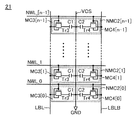
- the NVM 21 shown in FIG. 4 is a memory circuit having n NMCs 2.
- NMC2 has MC3 and MC4.
- MC3 is a modification of MC1, and a transistor Tr3 is provided instead of the transistor Tr1.
- MC4 is a modification of MC2, and a transistor Tr4 is provided instead of the transistor Tr2.
- the transistor Tr3 is provided with a second gate, and the second gate and the first gate are electrically connected.
- the transistor Tr4 is provided with a second gate, and the second gate and the first gate are electrically connected. By electrically connecting the second gate and the first gate, the on-state current of the transistors Tr3 and Tr4 can be improved.
- the transistors Tr1 and Tr2 of the NVM 20 may be OS transistors, and the other transistors may be Si transistors, for example.
- the memory cell array 110 can have a device structure in which a circuit composed of OS transistors is stacked on a circuit composed of Si transistors.
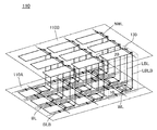
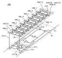
- FIG. 5 schematically shows a device structure example of the memory cell array 110.
- the memory cell array 110B is stacked on the memory cell array 110A.
- the memory cell array 110A is provided with SMCs 10 and LPCs 30 in a matrix.
- the memory cell array 110B is provided with NVMs 20 in a matrix.
- the memory cell array 110A constitutes a memory part A having a high response speed, and the memory cell array 110B constitutes a memory part B for long-term storage of data.
- FIG. 6 is a circuit diagram schematically showing a device structure example of the memory cell 130.
- FIG. 6 shows an example in which the NVM 20 has a circuit configuration for storing 8-bit complementary data. Therefore, the NVM 20 includes NMC [0] to NMC [7]. NMC [0] to NMC [7] are provided on the region where the SMC 10 and the LPC 30 are formed.
- the configuration of the memory cell 130 described so far (a configuration in which two complementary memory cells (MC1 and MC2) are connected to one wiring NWL) is referred to as a twin cell type.
- the number of NMCs is preferably a multiple of 8. That is, the number of data bits that can be held by the NVM 20 is preferably a multiple of eight.
- the memory cell 130 can handle data for each unit such as 1 byte (8 bits), 1 word (32 bits), halfword (16 bits), and the like.
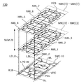
- FIG. 7 shows a device structure example of the memory cell 130 when the memory cell array 110B has a two-layer structure.
- the NVM 20 has NMC [0] to NMC [7].
- NMC [0] to NMC [3] are stacked on the region where the SMC 10 and the LPC 30 are formed, and NMC [4] to NMC [7] are stacked on the region where the NMC [0] to NMC [3] are formed.
- NMC [0] to NMC [3] are stacked on the region where the SMC 10 and the LPC 30 are formed.
- NMC [4] to NMC [7] are stacked on the region where the NMC [0] to NMC [3] are formed.
- the memory cell array 110 By stacking the memory cell array 110B on the memory cell array 110A, the memory cell array 110 can be increased in capacity and size.
- the area per bit of the memory cell array 110 is the area of one NMC. That is, the area per bit is the area of a region where two transistors and two capacitors are provided.
- the area per bit of the memory cell array 110 is 1 ⁇ 2 of the example of FIG. In this manner, by providing the NVM 20 in a stacked manner on the SMC 10, the area per bit of the memory cell 130 is smaller than that of the CMOS SRAM memory cell.
- the memory cell array 110B composed of the NVM 20 has a very high affinity with a CMOS circuit compared to other nonvolatile memories such as a flash memory, an MRAM (magnetoresistance random access memory), and a PRAM (phase change random access memory).
- a flash memory requires a high voltage for driving. Since MRAM and PRAM are current drive type memories, elements and circuits for current drive are required.
- the NVM 20 operates by controlling on and off of the transistors Tr1 and Tr2.
- the NVM 20 is a circuit composed of voltage-driven transistors like the CMOS circuit, and can be driven with a low voltage. Therefore, it is easy to incorporate the processor and the storage device 100 into one chip. Further, the storage device 100 can reduce the area per bit without degrading the performance. Further, the storage device 100 can reduce power consumption. Further, since the storage device 100 can store data even when the power is turned off, the power gating of the storage device 100 is possible.
- SRAM is used for standard processor on-chip cache memory because it is fast.
- SRAM has the disadvantages that it consumes power even during standby and that it is difficult to increase the capacity. For example, in a processor for a mobile device, it is said that power consumption during standby of the on-chip cache memory reaches 80% of the average power consumption of the entire processor.
- the storage device 100 is a RAM in which the disadvantages of the SRAM are eliminated while taking advantage of the advantages of the SRAM that reading and writing are fast. Therefore, applying the storage device 100 to the on-chip cache memory is useful for reducing the power consumption of the entire processor.
- FIG. 8 shows an example in which a folded type is applied to the memory cell 130.
- the NMC is composed of two transistors and two capacitors.
- the NMC is composed of one transistor and one capacitor. It consists of
- NMCs are classified into those connected to the wiring LBL and those connected to the wiring LBLB.
- FIG. 9 shows an example in which an open type is applied to the memory cell 130.
- the NMC is composed of one transistor and one capacitor.
- NWL the number of NMCs
- the open-type memory cell 130 NMC is classified into one connected to the wiring LBL and one connected to the wiring LBLB.
- the open type can highly integrate NMC, and the capacity of data that can be stored in the storage device 100 can be increased as compared with the twin cell type and the folded type.
- the twin cell type memory cell 130 treats complementary data held in two capacitor elements as one bit, but the folded type and open type memory cell 130 uses one bit of data held in one capacitor element. Treat as. In other cases, the description of the twin-cell type operation can be referred to for the folding and opening type operations.
- the storage device 100 can reduce static power.
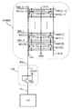
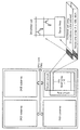
- FIG. 10 shows the NVM 20, the voltage holding circuit 128 connected to the NVM 20, and the voltage generation circuit 127 connected to the voltage holding circuit 128.
- the voltage holding circuit 128 includes a transistor OS1 and a capacitor C0.
- the first terminal of the transistor OS1 is electrically connected to the first gate of the transistor OS1, the second gate of the transistor OS1, the first terminal of the capacitor C0, and the wiring BGL.
- Second terminal of the transistor OS1 is given a voltage V BG is electrically connected to the voltage generation circuit 127. Note that in the following description, the transistor OS1 is described as an n-channel transistor.
- the voltage holding circuit 128 has a function of writing a potential to the second gates of the transistors Tr1 and Tr2 and holding the potential. For example, when the voltage holding circuit 128 writes a negative potential to the second gates of the transistors Tr1 and Tr2, the transistors Tr1 and Tr2 increase Vth while the negative potential of the second gate of the transistors Tr1 and Tr2 is held. Can keep. By keeping Vth high for the transistors Tr1 and Tr2, normally-on can be prevented and the power consumption of the storage device 100 can be reduced.
- the first gate and the second gate preferably have regions overlapping with each other with the semiconductor layer interposed therebetween. Further, the above OS transistor is preferably used as the transistor OS1.
- a drain current hereinafter referred to as a cut-off current
- the voltage holding circuit 128 can apply a negative potential applied to the wiring BGL for a long time. Can be held.
- the channel length of the transistor OS1 is preferably longer than the channel lengths of the transistors Tr1 and Tr2.
- the channel length of the transistor OS1 is 1 ⁇ m or more, more preferably 3 ⁇ m or more, further preferably 5 ⁇ m or more, and further preferably 10 ⁇ m or more.
- the transistor OS1 By increasing the channel length of the transistor OS1, the transistor OS1 is not affected by the short channel effect, and the cut-off current can be kept low. In addition, the transistor OS1 can increase the withstand voltage between the source and the drain. A high breakdown voltage between the source and drain of the transistor OS1 is preferable because the connection between the voltage generation circuit 127 that generates a high voltage and the transistor OS1 can be facilitated.
- the transistor OS1 Since the transistor OS1 is used in a circuit that requires a high degree of integration such as a memory cell, it is preferable that the channel lengths of the transistors Tr1 and Tr2 be short. On the other hand, since the voltage holding circuit 128 is formed outside the memory cell, there is no problem even if the channel length of the transistor OS1 is long. Further, when the channel length of the transistor is increased, the on-state current of the transistor is reduced. However, since the transistor OS1 is often used mainly in an off state, a high on-state current is not required.
- the voltage generation circuit 127 has a function of generating a negative potential (V BG ).
- the circuit diagram shown in FIG. 11 shows an example of the voltage generation circuit 127.
- These circuits are step-down charge pumps, in which GND is input to the input terminal IN and VBG is output from the output terminal OUT.
- the number of stages of the basic circuit of the charge pump circuit is four, but the present invention is not limited to this, and the charge pump circuit may be configured with an arbitrary number of stages.
- a voltage generation circuit 127a illustrated in FIG. 11A includes transistors M21 to M24 and capacitor elements C21 to C24.
- the transistors M21 to M24 are described as n-channel transistors.
- the transistors M21 to M24 are connected in series between the input terminal IN and the output terminal OUT, and are connected so that each gate and the first electrode function as a diode.
- Capacitance elements C21 to C24 are connected to the gates of the transistors M21 to M24, respectively.
- CLK is input to the first electrodes of the odd-numbered capacitive elements C21 and C23
- CLKB is input to the first electrodes of the even-numbered capacitive elements C22 and C24.
- CLKB is an inverted clock signal obtained by inverting the phase of CLK.
- Voltage generating circuit 127a has a function of stepping down the input to the input terminal IN GND, generates a V BG.
- the voltage generation circuit 127a can generate a negative potential only by supplying CLK and CLKB.
- the above-described transistors M21 to M24 may be formed of OS transistors.
- the use of the OS transistor is preferable because the reverse current of the diode-connected transistors M21 to M24 can be reduced.
- a voltage generation circuit 127b illustrated in FIG. 11B includes transistors M31 to M34 which are p-channel transistors. For other components, the description of the voltage generation circuit 127a is cited.
- the memory device 100 can reduce power consumption and circuit area by using the above structure.
- Embodiment 2 In this embodiment, a configuration example of the storage device 100 described in Embodiment 1 is described.
- FIG. 12 shows an example of a cross-sectional view of the storage device 100.
- a storage device 100 illustrated in FIG. 12 includes a layer L1, a layer L2, a layer L3, and a layer L4 which are stacked in order from the bottom.
- the layer L1 includes a transistor M1, a substrate 300, an element isolation layer 301, an insulator 302, a plug 310, and the like.
- the layer L2 includes an insulator 303, a wiring 320, an insulator 304, a plug 311, and the like.
- the layer L3 includes an insulator 214, an insulator 216, a transistor Tr1, a plug 312, an insulator 282, a wiring 321, and the like.
- the first gate of the transistor Tr1 has a function as the wiring NWL
- the second gate of the transistor Tr1 has a function as the wiring BGL.
- the layer L4 includes a capacitor C1, a plug 313, a wiring LBL, and the like.
- the capacitor element C1 includes a conductor 322, a conductor 323, and an insulator 305.
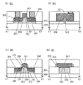
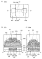
- FIG. 14A is a cross-sectional view in the channel length direction of the transistor M1
- FIG. 14B is a cross-sectional view in the channel width direction of the transistor M1.
- the transistor M1 is provided over the substrate 300 and is isolated from other adjacent transistors by an element isolation layer 301.
- an element isolation layer 301 silicon oxide, silicon oxynitride, silicon nitride oxide, silicon nitride, or the like can be used. Note that in this specification, an oxynitride refers to a compound having a higher oxygen content than nitrogen, and a nitride oxide refers to a compound having a higher nitrogen content than oxygen.
- a single crystal semiconductor substrate made of silicon or silicon carbide, a polycrystalline semiconductor substrate, a compound semiconductor substrate made of silicon germanium, an SOI (Silicon On Insulator) substrate, or the like can be used.
- a glass substrate, a quartz substrate, a plastic substrate, a metal substrate, a bonded film, paper containing a fibrous material, or a base film may be used.
- a semiconductor element may be formed using a certain substrate, and then the semiconductor element may be transferred to another substrate.
- a flexible substrate may be used as the substrate 300.
- a method for providing a transistor over a flexible substrate there is a method in which after a transistor is formed over a non-flexible substrate, the transistor is peeled off and transferred to the substrate 300 which is a flexible substrate.
- a separation layer is preferably provided between the non-flexible substrate and the transistor.
- a sheet, a film, a foil, or the like in which fibers are knitted may be used as the substrate 300.
- the substrate 300 may have elasticity. Further, the substrate 300 may have a property of returning to the original shape when bending or pulling is stopped. Or you may have a property which does not return to an original shape.
- the thickness of the substrate 300 is, for example, 5 ⁇ m to 700 ⁇ m, preferably 10 ⁇ m to 500 ⁇ m, more preferably 15 ⁇ m to 300 ⁇ m.
- the semiconductor device can be reduced in weight. Further, by reducing the thickness of the substrate 300, there is a case where the substrate 300 is stretchable even when glass or the like is used, or when the bending or pulling is stopped, the substrate 300 may return to the original shape. Therefore, an impact applied to the semiconductor device on the substrate 300 due to a drop or the like can be reduced. That is, a durable semiconductor device can be provided.
- the substrate 300 which is a flexible substrate, for example, metal, alloy, resin, glass, or fiber thereof can be used.
- the substrate 300 which is a flexible substrate, is preferable because the deformation due to the environment is suppressed as the linear expansion coefficient is lower.
- the substrate 300 which is a flexible substrate for example, a material whose linear expansion coefficient is 1 ⁇ 10 ⁇ 3 / K or less, 5 ⁇ 10 ⁇ 5 / K or less, or 1 ⁇ 10 ⁇ 5 / K or less is used. Good.
- the resin include polyester, polyolefin, polyamide (such as nylon and aramid), polyimide, polycarbonate, acrylic, and polytetrafluoroethylene (PTFE).
- aramid has a low coefficient of linear expansion, it is suitable for the substrate 300 that is a flexible substrate.
- a transistor M1 illustrated in FIGS. 14A and 14B includes a channel formation region 352, an impurity region 353, and an impurity region 354 provided in the well 351, a conductive region 355 provided in contact with the impurity region, and a conductive region. 356, a gate insulator 358 provided over the channel formation region 352, and a gate electrode 357 provided over the gate insulator 358. Note that metal silicide or the like may be used for the conductive regions 355 and 356.
- the channel formation region 352 has a convex shape, and a gate insulator 358 and a gate electrode 357 are provided along a side surface and an upper surface thereof (see FIG. 14B).
- a transistor having such a shape is referred to as a FIN transistor.
- a semiconductor layer having a convex shape may be formed by processing an SOI substrate.
- a Si transistor is applied as the transistor M1.
- the transistor M1 may be either an n-channel transistor or a p-channel transistor, and an appropriate transistor may be used depending on a circuit.
- FIGS. 14C is a cross-sectional view in the channel length direction of the transistor M1
- FIG. 14D is a cross-sectional view in the channel width direction of the transistor M1.
- a transistor M1 illustrated in FIGS. 14C and 14D includes a channel formation region 362, a low concentration impurity region 371, a low concentration impurity region 372, a high concentration impurity region 363, and a high concentration impurity region 364 provided in the well 361.
- a conductive region 365 and a conductive region 366 provided in contact with the high-concentration impurity region; a gate insulator 368 provided over the channel formation region 362; and a gate electrode provided over the gate insulator 368. 367, and a sidewall insulating layer 369 and a sidewall insulating layer 370 provided on the sidewall of the gate electrode 367.
- metal silicide or the like may be used for the conductive regions 365 and 366.
- the insulator 302 functions as an interlayer insulator.
- the insulator 302 preferably contains hydrogen.
- silicon oxide, silicon oxynitride, silicon nitride oxide, silicon nitride, or the like is preferably used.
- the insulator 303 it is preferable to use a barrier film from which hydrogen or impurities are not diffused from the substrate 300, the transistor M1, or the like into a region where the transistor Tr1 is provided.
- a barrier film from which hydrogen or impurities are not diffused from the substrate 300, the transistor M1, or the like into a region where the transistor Tr1 is provided For example, silicon nitride formed by a CVD method can be used. When hydrogen diffuses into the oxide semiconductor included in the transistor Tr1, the characteristics of the oxide semiconductor may be deteriorated. Therefore, it is preferable to use a film that suppresses diffusion of hydrogen between the transistor M1 and the transistor Tr1.
- the film that suppresses the diffusion of hydrogen refers to a film with a small amount of hydrogen desorption.
- the amount of desorption of hydrogen can be analyzed using, for example, a temperature desorption gas analysis method (TDS (Thermal Desorption Spectroscopy)).
- TDS Temperatur Desorption Spectroscopy
- the amount of hydrogen desorbed from the insulator 324 is 10 ⁇ 10 5 in terms of the amount of desorbed hydrogen converted to the area of the insulator 303 in the range of 50 ° C. to 500 ° C. in TDS analysis. It may be 15 atoms / cm 2 or less, preferably 5 ⁇ 10 15 atoms / cm 2 or less.
- the insulators 304, 214, and 282 are preferably insulators that suppress copper diffusion or have barrier properties against oxygen and hydrogen.
- silicon nitride can be used as an example of a film that suppresses copper diffusion.
- a metal oxide such as aluminum oxide may be used.
- insulator 216 for example, a silicon oxide film, a silicon oxynitride film, or the like can be used.
- silicon oxide, silicon oxynitride, silicon nitride oxide, silicon nitride, aluminum oxide, aluminum oxynitride, aluminum nitride oxide, aluminum nitride, hafnium oxide, hafnium oxynitride, hafnium nitride oxide, hafnium nitride, or the like is used. That's fine.
- the insulator 305 may have a stacked structure of the above insulators.
- a stacked structure of a material having high dielectric breakdown resistance such as silicon oxynitride and a high dielectric constant (high-k) material such as aluminum oxide may be used.
- high-k high dielectric constant
- a single layer or a laminate of a simple substance made of a low-resistance material, an alloy, or a conductor containing a compound containing these as a main component In particular, it is preferable to use a high melting point material such as tungsten or molybdenum that has both heat resistance and conductivity.
- low resistance conductive materials such as aluminum and copper.
- the transistor Tr1 may be formed over the capacitor C1.
- a cross-sectional view in that case is shown in FIG.
- the layer L3 and the layer L4 are different from the cross-sectional view of FIG.
- the layer L3 includes a wiring 341 and a capacitor C1.
- the layer L4 includes a plug 331, a plug 332, a plug 333, a plug 334, a wiring 342, a wiring 343, a wiring LBL, an insulator 214, an insulator 216, an insulator 280, an insulator 282, and a transistor Tr1.
- the transistor Tr1 By providing the capacitor C1 below the transistor Tr1, the transistor Tr1 can be prevented from the process damage or the influence of hydrogen that occurs when the capacitor C1 is formed.
- a region to which no code or hatching pattern is given is made of an insulator.
- the insulator include aluminum oxide, aluminum nitride oxide, magnesium oxide, silicon oxide, silicon oxynitride, silicon nitride oxide, silicon nitride, gallium oxide, germanium oxide, yttrium oxide, zirconium oxide, lanthanum oxide, neodymium oxide, and hafnium oxide.
- An insulator containing one or more materials selected from tantalum oxide and the like can be used.
- an organic resin such as a polyimide resin, a polyamide resin, an acrylic resin, a siloxane resin, an epoxy resin, or a phenol resin can be used.
- the oxide semiconductor preferably contains at least indium or zinc. In particular, it is preferable to contain indium and zinc. Here, a case where the oxide semiconductor includes indium, the element M, and zinc is considered.
- gallium (Ga) is preferable.
- other elements applicable to the element M aluminum (Al), boron (B), silicon (Si), titanium (Ti), zirconium (Zr), lanthanum (La), cerium (Ce), yttrium (Y ), Hafnium (Hf), tantalum (Ta), niobium (Nb), scandium (Sc), and the like.
- FIGS. 15A, 15B, and 15C a preferable range of the atomic ratio of indium, the element M, and zinc included in the oxide semiconductor according to the present invention will be described.
- FIG. 15 does not describe the atomic ratio of oxygen.
- the terms of the atomic ratio of indium, element M, and zinc included in the oxide semiconductor are [In], [M], and [Zn].
- [In]: [M]: [Zn] (1 + ⁇ ): (1- ⁇ ): 4 atoms
- a grain boundary also referred to as a grain boundary
- the carrier mobility (electron mobility) of the oxide semiconductor can be increased. This is because, in an oxide semiconductor containing indium, element M, and zinc, the s orbital of heavy metal mainly contributes to carrier conduction, and by increasing the indium content, the region where the s orbital overlaps becomes larger. It is.
- a region indicated by a region A in FIG. 15A represents a region in which the oxide semiconductor has a high carrier mobility and easily has a layered structure with few grain boundaries.
- An oxide semiconductor having an atomic ratio represented by the region B is an excellent oxide semiconductor particularly having high crystallinity and high carrier mobility.
- 16A to 16C are a top view and a cross-sectional view of the transistor 200a.
- 16A is a top view
- FIG. 16B is a cross-sectional view corresponding to the alternate long and short dash line X1-X2 shown in FIG. 16A
- FIG. 16C is a cross-sectional view corresponding to the alternate long and short dash line Y1-Y2. . Note that in the top view of FIG. 16A, some elements are omitted for clarity.
- 16B and 16C illustrate an example in which the transistor 200a is provided over the insulator 214 and the insulator 216.
- the transistor 200a includes a conductor 205 (a conductor 205a and a conductor 205b) and a conductor 260 which function as a gate electrode, an insulator 220, an insulator 222, an insulator 224, and an insulator 250 which function as a gate insulating layer.
- An oxide semiconductor 230 oxide semiconductor 230a, oxide semiconductor 230b, and oxide semiconductor 230c
- a conductor 240a that functions as one of a source or a drain
- a conductor 240b that functions as the other of a source or a drain
- an insulator 241 that protects the conductor 260 and an insulator 280 having excess oxygen (containing oxygen in excess of the stoichiometric composition).
- the conductor 260 may be referred to as a top gate and the conductor 205 may be referred to as a bottom gate.
- the conductor 260 may be referred to as a first gate and the conductor 205 may be referred to as a second gate.
- the oxide semiconductor 230 includes an oxide semiconductor 230a, an oxide semiconductor 230b over the oxide semiconductor 230a, and an oxide semiconductor 230c over the oxide semiconductor 230b. Note that when the transistor 200a is turned on, a current flows mainly in the oxide semiconductor 230b; thus, the oxide semiconductor 230b functions as a channel formation region. On the other hand, in the oxide semiconductor 230a and the oxide semiconductor 230c, current may flow near the interface with the oxide semiconductor 230b (which may be a mixed region), but the other regions function as insulators. There is a case.
- the conductor 205 includes a metal film containing an element selected from molybdenum, titanium, tantalum, tungsten, aluminum, copper, chromium, neodymium, and scandium, or a metal nitride film containing any of the above-described elements (a titanium nitride film or a nitride film). Molybdenum film, tungsten nitride film) and the like. Or indium tin oxide, indium oxide containing tungsten oxide, indium zinc oxide containing tungsten oxide, indium oxide containing titanium oxide, indium tin oxide containing titanium oxide, indium zinc oxide, silicon oxide added It is also possible to apply a conductive material such as indium tin oxide.
- FIG. 16B illustrates a two-layer structure of the conductor 205a and the conductor 205b; however, the structure is not limited thereto, and a single layer or a stacked structure including three or more layers may be used.
- the insulator 220 and the insulator 224 are preferably insulators containing oxygen such as a silicon oxide film or a silicon oxynitride film.
- an insulator containing excess oxygen is preferably used as the insulator 224.
- an insulator including a material such as silicon nitride, silicon nitride oxide, aluminum oxide, hafnium oxide, tantalum oxide, or zirconium oxide is preferably used as a single layer or a stacked layer.
- Vth can be controlled by appropriately adjusting the film thicknesses of the insulator 220, the insulator 222, and the insulator 224.
- a transistor with low leakage current when not conducting can be provided. It is preferable to reduce the thickness of each of the insulator 220, the insulator 222, and the insulator 224 because Vth control by the conductor 205 is facilitated.
- the thickness of each of the insulator 220, the insulator 222, and the insulator 224 may be 50 nm or less, more preferably 30 nm or less, more preferably 10 nm or less, and still more preferably 5 nm or less.
- the oxide semiconductor 230a, the oxide semiconductor 230b, and the oxide semiconductor 230c are formed using a metal oxide such as an In-M-Zn oxide. Further, as the oxide semiconductor 230, an In—Ga oxide or an In—Zn oxide may be used.
- the energy level at the lower end of the conduction band is closer to the vacuum level than the oxide semiconductor 230b, typically, the energy level at the lower end of the conduction band of the oxide semiconductor 230b;
- the difference from the energy level at the lower end of the conduction band of the oxide semiconductor 230a and the oxide semiconductor 230c is preferably 0.15 eV or more, 0.5 eV or more, 2 eV or less, or 1 eV or less.
- the difference between the electron affinity of the oxide semiconductor 230a and the oxide semiconductor 230c and the electron affinity of the oxide semiconductor 230b is 0.15 eV or more, or 0.5 eV or more, and 2 eV or less, or 1 eV or less. preferable.
- the energy gap is preferably 2 eV or more, and more preferably 2.5 eV or more and 3.0 eV or less.
- the energy gap is preferably 2 eV or more, more preferably 2.5 eV or more, and further preferably 2.7 eV or more and 3.5 eV or less.
- the energy gap between the oxide semiconductor 230a and the oxide semiconductor 230c is preferably larger than the energy gap between the oxide semiconductor 230b.
- the energy gap between the oxide semiconductor 230a and the oxide semiconductor 230c is 0.15 eV or more, 0.5 eV or more, 1.0 eV or more, and 2 eV or less, or 1 eV, compared to the energy gap of the oxide semiconductor 230b.
- the following is preferable.
- the thicknesses of the oxide semiconductor 230a, the oxide semiconductor 230b, and the oxide semiconductor 230c are 3 nm to 200 nm, preferably 3 nm to 100 nm, and more preferably 3 nm to 60 nm.
- oxygen vacancies (Vo) in the oxide semiconductor, impurities in the oxide semiconductor, and the like can be given.
- the density of defect states is increased when hydrogen is bonded to the oxygen vacancies (this state is also referred to as VoH).
- the carrier density of an oxide semiconductor can be controlled by controlling the density of defect states in the oxide semiconductor.
- High purity intrinsic or substantially high purity intrinsic Low impurity concentration and low defect level density are referred to as high purity intrinsic or substantially high purity intrinsic.
- a highly purified intrinsic or substantially highly purified intrinsic oxide semiconductor film has few carrier generation sources, and thus can have a low carrier density.
- the oxide semiconductor 230a and the oxide semiconductor 230c it is preferable to use an oxide semiconductor that is highly purified intrinsic or substantially highly purified intrinsic.
- the carrier density of the oxide semiconductor 230a and the oxide semiconductor 230c is less than 8 ⁇ 10 15 cm ⁇ 3 , preferably less than 1 ⁇ 10 11 cm ⁇ 3 , more preferably less than 1 ⁇ 10 10 cm ⁇ 3 , What is necessary is just to set it as 1 * 10 ⁇ -9 > cm ⁇ -3 > or more.
- the carrier density of the oxide semiconductor for the purpose of improving the on-state current of the transistor or improving the field-effect mobility of the transistor, it is preferable to increase the carrier density of the oxide semiconductor.
- the impurity concentration of the oxide semiconductor may be slightly increased or the defect state density of the oxide semiconductor may be slightly increased.
- the band gap of the oxide semiconductor is preferably made smaller. For example, in a range where the on / off ratio of I D -V G characteristics of the transistor can be taken, slightly higher impurity concentration, or density of defect states slightly higher oxide semiconductor can be regarded as substantially intrinsic.
- an oxide semiconductor having a high electron affinity and a reduced band gap and, as a result, an increased density of thermally excited electrons (carriers) can be regarded as substantially intrinsic. Note that in the case where an oxide semiconductor having higher electron affinity is used, the threshold voltage of the transistor becomes lower.
- the carrier density of the oxide semiconductor 230b is preferably higher than that of the oxide semiconductor 230a and the oxide semiconductor 230c.
- the carrier density of the oxide semiconductor 230b is preferably less than 1 ⁇ 10 5 cm -3 or more 1 ⁇ 10 18 cm -3, more preferably 1 ⁇ 10 7 cm -3 or more than 1 ⁇ 10 17 cm -3, 1 ⁇ 10 9 cm ⁇ 3 or more and 5 ⁇ 10 16 cm ⁇ 3 or less are more preferable, 1 ⁇ 10 10 cm ⁇ 3 or more and 1 ⁇ 10 16 cm ⁇ 3 or less are more preferable, and 1 ⁇ 10 11 cm ⁇ 3 or more and 1 ⁇ 10 15 or less. More preferably, it is cm ⁇ 3 or less.
- the defect state density of the mixed layer formed at the interface between the oxide semiconductor 230a and the oxide semiconductor 230b or the interface between the oxide semiconductor 230b and the oxide semiconductor 230c be reduced.
- the oxide semiconductor 230a and the oxide semiconductor 230b, and the oxide semiconductor 230b and the oxide semiconductor 230c have a common element (main component) in addition to oxygen, so that the density of defect states is low.
- a layer can be formed.
- the oxide semiconductor 230b is an In—Ga—Zn oxide semiconductor
- an In—Ga—Zn oxide semiconductor, a Ga—Zn oxide semiconductor, gallium oxide, or the like is used as the oxide semiconductor 230a and the oxide semiconductor 230c. Good.
- the main path of carriers is the oxide semiconductor 230b. Since the defect level density at the interface between the oxide semiconductor 230a and the oxide semiconductor 230b and the interface between the oxide semiconductor 230b and the oxide semiconductor 230c can be lowered, the influence on carrier conduction due to interface scattering is small. High on-current can be obtained.
- the trapped electrons behave like fixed charges, and thus the Vth of the transistor shifts in the positive direction.
- the trap level can be kept away from the oxide semiconductor 230b. With this structure, Vth of the transistor can be prevented from shifting in the plus direction.
- the oxide semiconductor 230a and the oxide semiconductor 230c are formed using a material whose conductivity is sufficiently lower than that of the oxide semiconductor 230b.
- the oxide semiconductor 230b, the interface between the oxide semiconductor 230b and the oxide semiconductor 230a, and the interface between the oxide semiconductor 230b and the oxide semiconductor 230c mainly function as a channel region.
- the oxide semiconductor 230b In particular, in the case where an oxide semiconductor having an atomic ratio represented by the region A illustrated in FIG. 15A is used for the oxide semiconductor 230b, [M] / [In] is included in the oxide semiconductor 230a and the oxide semiconductor 230c. It is preferable to use an oxide semiconductor that is 1 or more, preferably 2 or more. As the oxide semiconductor 230c, it is preferable to use an oxide semiconductor in which [M] / ([Zn] + [In]) is 1 or more, which can obtain sufficiently high insulation.
- the oxide semiconductor 230c may have lower crystallinity than the oxide semiconductor 230b.
- the oxide semiconductor 230b preferably includes a CAAC-OS which will be described later.
- the oxide semiconductor 230c may be amorphous or a-like (amorphous-like oxide semiconductor) described later.
- the oxide semiconductor 230a may include a CAAC-OS.
- the oxide semiconductor 230a preferably has higher crystallinity than the oxide semiconductor 230c.
- the insulator 250 is formed of, for example, silicon oxide, silicon oxynitride, silicon nitride oxide, aluminum oxide, hafnium oxide, tantalum oxide, zirconium oxide, lead zirconate titanate (PZT), strontium titanate (SrTiO 3 ), or (Ba,
- An insulator including a material such as Sr) TiO 3 (BST) can be used in a single layer or a stacked layer.
- aluminum oxide, bismuth oxide, germanium oxide, niobium oxide, silicon oxide, titanium oxide, tungsten oxide, yttrium oxide, or zirconium oxide may be added to these insulators.
- these insulators may be nitrided. Silicon insulator, silicon oxynitride, or silicon nitride may be stacked over the above insulator.
- an oxide insulator containing more oxygen than that in the stoichiometric composition is preferably used as in the insulator 224.
- an oxide insulator containing excess oxygen in contact with the oxide semiconductor 230 oxygen vacancies in the oxide semiconductor 230 can be reduced.
- the insulator 250 can be formed using an insulating film having a barrier property against oxygen and hydrogen, such as aluminum oxide, aluminum oxynitride, hafnium oxide, hafnium oxynitride, and silicon nitride. In the case of using such a material, it functions as a layer which prevents release of oxygen from the oxide semiconductor 230 and entry of impurities such as hydrogen from the outside.
- an insulating film having a barrier property against oxygen and hydrogen such as aluminum oxide, aluminum oxynitride, hafnium oxide, hafnium oxynitride, and silicon nitride.
- a metal such as aluminum, titanium, chromium, nickel, copper, yttrium, zirconium, molybdenum, silver, tantalum, or tungsten, or an alloy containing the same as a main component can be used. Further, although a single layer structure is shown in the figure, a stacked structure of two or more layers may be used.
- a titanium film and an aluminum film may be stacked.
- a two-layer structure in which an aluminum film is stacked on a tungsten film a two-layer structure in which a copper film is stacked on a copper-magnesium-aluminum alloy film, a two-layer structure in which a copper film is stacked on a titanium film, and a tungsten film
- a two-layer structure in which copper films are stacked may be used.
- a transparent conductive material containing indium oxide, tin oxide, or zinc oxide may be used.
- the conductor 260 having a function as a gate electrode is, for example, a metal selected from aluminum, chromium, copper, tantalum, titanium, molybdenum, tungsten, an alloy containing the above-described metal as a component, or a combination of the above-described metals. It can be formed using an alloy or the like. Further, a metal selected from one or more of manganese and zirconium may be used. Alternatively, a semiconductor typified by polycrystalline silicon doped with an impurity element such as phosphorus, or silicide such as nickel silicide may be used.
- a two-layer structure in which a titanium film is stacked over aluminum is preferable.
- a two-layer structure in which a titanium film is stacked on a titanium nitride film, a two-layer structure in which a tungsten film is stacked on a titanium nitride film, or a two-layer structure in which a tungsten film is stacked on a tantalum nitride film or a tungsten nitride film may be employed. .
- titanium film and a three-layer structure in which an aluminum film is stacked on the titanium film and a titanium film is further formed thereon.
- an alloy film or a nitride film in which one or more metals selected from aluminum, titanium, tantalum, tungsten, molybdenum, chromium, neodymium, and scandium are combined may be used.
- the conductor 260 includes indium tin oxide, indium oxide including tungsten oxide, indium zinc oxide including tungsten oxide, indium oxide including titanium oxide, indium tin oxide including titanium oxide, and indium zinc oxide.
- a light-transmitting conductive material such as indium tin oxide to which silicon oxide is added can be used.
- a stacked structure of the above light-transmitting conductive material and the above metal can be used.
- the Vth of the transistor 200a can be increased and the cut-off current can be reduced.
- the work function of the conductor 260 is preferably 4.8 eV or more, more preferably 5.0 eV or more, more preferably 5.2 eV or more, more preferably 5.4 eV or more, more preferably 5.6 eV or more. May be used.
- the conductive material having a high work function include molybdenum, molybdenum oxide, Pt, Pt silicide, Ni silicide, indium tin oxide, and nitrogen-added In—Ga—Zn oxide.
- An insulator 241 is provided so as to cover the conductor 260.
- the insulator 241 can be formed using an insulating film having a barrier property against oxygen or hydrogen, such as aluminum oxide, aluminum oxynitride, hafnium oxide, hafnium oxynitride, or silicon nitride. When formed using such a material, the conductor 260 can be prevented from being oxidized by the heat treatment step. Note that the insulator 241 can be omitted by using a material that is difficult to oxidize for the conductor 260.
- An insulator 280 is provided above the transistor 200a.
- the insulator 280 preferably contains excess oxygen.
- reliability can be improved by reducing oxygen vacancies in the transistor 200a.
- an oxide material from which part of oxygen is released by heating is preferably used as the insulator having excess oxygen.
- the oxide which desorbs oxygen by heating means that the amount of desorbed oxygen converted to oxygen atoms is 1.0 ⁇ 10 18 atoms / cm 3 or more, preferably 3.0 ⁇ 10 20 in TDS analysis.
- An oxide film having atoms / cm 3 or more. The surface temperature of the film at the time of the TDS analysis is preferably in the range of 100 ° C. to 700 ° C., or 100 ° C. to 500 ° C.
- a material containing silicon oxide or silicon oxynitride is preferably used.
- a metal oxide can be used.
- the insulator 280 that covers the transistor 200a may function as a planarization film that covers the uneven shape below the transistor 200a.
- 17A to 17C are a top view and a cross-sectional view of the transistor 200b.
- 17A is a top view
- FIG. 17B is a cross-sectional view corresponding to the dashed-dotted line X1-X2 shown in FIG. 17A
- FIG. 17C is a cross-sectional view corresponding to the dashed-dotted line Y1-Y2. . Note that in the top view of FIG. 17A, some elements are omitted for clarity.
- the transistor 200b is different from the transistor 200a in that an oxide semiconductor 230c, an insulator 250, and a conductor 260 are formed in an opening formed in the insulator 280.
- the transistor 200b has a structure in which the conductors 240a and 240b and the conductor 260 hardly overlap with each other, the parasitic capacitance applied to the conductor 260 can be reduced. That is, a transistor with a high operating frequency can be provided.
- the description of the transistor 200a may be referred to.
- FIG. 18A to 18C are a top view and a cross-sectional view of the transistor 200c.
- 18A is a top view
- FIG. 18B is a cross-sectional view corresponding to the alternate long and short dash line X1-X2 shown in FIG. 18A
- FIG. 18C is a cross-sectional view corresponding to the alternate long and short dash line Y1-Y2. . Note that in the top view of FIG. 18A, some elements are omitted for clarity.
- a transistor 200c in FIG. 18 is different from the transistor 200a in that central portions of the oxide semiconductors 230a and 230b are etched (see FIG. 18B).
- the transistor 200a has a channel formed in the oxide semiconductor 230b, whereas the transistor 200c has a channel formed in the oxide semiconductor 230c.
- the oxide semiconductor 230c has a lower electron mobility and a wider band gap than the oxide semiconductor 230b. Therefore, the transistor 200c has a smaller on-state current than the transistor 200a but a smaller off-state current.
- the transistor 200c is suitable for a transistor in which off-state current is more important than on-state current.
- the transistor 200c can be formed at the same time as the transistor 200a.
- the transistor 200a is preferably used for a transistor that requires high on-state current, such as the transistors Tr1 and Tr2 in FIG. 2, and the transistor 200c is preferably used for a transistor that requires low off-state current, such as the transistor OS1 in FIG. .
- the description of the transistor 200a may be referred to.
- FIG. 19A to 19C are a top view and a cross-sectional view of the transistor 200d.
- 19A is a top view
- FIG. 19B is a cross-sectional view corresponding to the alternate long and short dash line X1-X2 shown in FIG. 19A
- FIG. 19B is a cross-sectional view corresponding to the alternate long and short dash line Y1-Y2. . Note that in the top view of FIG. 19A, some elements are omitted for clarity.
- the transistor 200d is different from the transistor 200b in that the central portions of the oxide semiconductors 230a and 230b are etched (see FIG. 19B).
- the transistor 200b has a channel formed in the oxide semiconductor 230b, whereas the transistor 200d has a channel formed in the oxide semiconductor 230c.
- the oxide semiconductor 230c has a lower electron mobility and a wider band gap than the oxide semiconductor 230b. Therefore, the transistor 200d has a smaller on-state current but a smaller off-state current than the transistor 200b.
- the transistor 200d is suitable for a transistor in which off-state current is more important than on-state current.
- the transistor 200d can be formed at the same time as the transistor 200b.
- the transistor 200b is preferably used for a transistor that requires high on-state current, such as the transistors Tr1 and Tr2 in FIG. 2, and the transistor 200d is preferably used for a transistor that requires low off-state current, such as the transistor OS1 in FIG. .
- the description of the transistor 200b may be referred to.
- parallel refers to a state in which two straight lines are arranged at an angle of ⁇ 10 ° to 10 °. Therefore, the case of ⁇ 5 ° to 5 ° is also included.
- substantially parallel means a state in which two straight lines are arranged at an angle of ⁇ 30 ° to 30 °.
- Vertical refers to a state in which two straight lines are arranged at an angle of 80 ° to 100 °. Therefore, the case of 85 ° to 95 ° is also included.
- substantially vertical means a state in which two straight lines are arranged at an angle of 60 ° to 120 °.
- An oxide semiconductor is classified into a single crystal oxide semiconductor and a non-single-crystal oxide semiconductor.
- a non-single-crystal oxide semiconductor a CAAC-OS (c-axis-aligned crystal oxide semiconductor), a polycrystalline oxide semiconductor, an nc-OS (nanocrystalline oxide semiconductor), a pseudo-amorphous oxide semiconductor (a-like oxide OS) : Amorphous-like oxide semiconductor) and amorphous oxide semiconductor.
- oxide semiconductors are classified into amorphous oxide semiconductors and other crystalline oxide semiconductors.
- a crystalline oxide semiconductor include a single crystal oxide semiconductor, a CAAC-OS, a polycrystalline oxide semiconductor, and an nc-OS.
- Amorphous structures are generally isotropic, have no heterogeneous structure, are metastable, have no fixed atomic arrangement, have a flexible bond angle, have short-range order, but long-range order It is said that it does not have.
- a stable oxide semiconductor cannot be called a complete amorphous oxide semiconductor.
- an oxide semiconductor that is not isotropic (for example, has a periodic structure in a minute region) cannot be called a complete amorphous oxide semiconductor.
- an a-like OS is not isotropic but has an unstable structure having a void (also referred to as a void). In terms of being unstable, a-like OS is physically similar to an amorphous oxide semiconductor.
- CAAC-OS First, the CAAC-OS will be described.
- a CAAC-OS is a kind of oxide semiconductor having a plurality of c-axis aligned crystal parts (also referred to as pellets).
- CAAC-OS is analyzed by X-ray diffraction (XRD: X-Ray Diffraction)
- XRD X-ray Diffraction
- the crystal has a c-axis orientation, and the plane on which the c-axis forms a CAAC-OS film (formation target) It can also be confirmed that it faces a direction substantially perpendicular to the upper surface.
- a peak may also appear when 2 ⁇ is around 36 °.
- the peak where 2 ⁇ is around 36 ° is attributed to the crystal structure classified into the space group Fd-3m. Therefore, the CAAC-OS preferably does not show the peak.
- CAAC-OS analyzed by electron diffraction will be described.
- an electron beam with a probe diameter of 300 nm is incident on a CAAC-OS including an InGaZnO 4 crystal in parallel to the formation surface of the CAAC-OS, spots caused by the (009) plane of the InGaZnO 4 crystal are generated.
- the included diffraction pattern appears. Therefore, electron diffraction shows that the pellets included in the CAAC-OS have c-axis alignment, and the c-axis is in a direction substantially perpendicular to the formation surface or the top surface.
- the CAAC-OS can also be referred to as an oxide semiconductor including CANC (C-Axis aligned nanocrystals).
- the pellet reflects the unevenness of the CAAC-OS formation surface or top surface and is parallel to the CAAC-OS formation surface or top surface.
- the pellet has a hexagonal shape.
- the shape of a pellet is not necessarily a regular hexagonal shape, and is often a non-regular hexagonal shape.
- CAAC-OS In the CAAC-OS, a clear crystal grain boundary cannot be confirmed.
- the CAAC-OS suppresses the formation of crystal grain boundaries by distorting the lattice arrangement. This is because the CAAC-OS can tolerate distortion due to the fact that the arrangement of oxygen atoms is not dense in the ab plane direction and the bond distance between atoms changes due to substitution of metal elements. This is probably because of this.
- the CAAC-OS has a c-axis alignment and a crystal structure in which a plurality of pellets (nanocrystals) are connected in the ab plane direction to have a strain. Therefore, the CAAC-OS can also be referred to as an oxide semiconductor having CAAcrystal (c-axis-aligned ab-plane-anchored crystal).
- the CAAC-OS is an oxide semiconductor with high crystallinity. Since the crystallinity of an oxide semiconductor may be deteriorated by entry of impurities, generation of defects, or the like, the CAAC-OS can be said to be an oxide semiconductor with few impurities and defects (such as oxygen vacancies).
- the impurity means an element other than the main components of the oxide semiconductor, such as hydrogen, carbon, silicon, or a transition metal element.
- an element such as silicon which has a stronger bonding force with oxygen than a metal element included in an oxide semiconductor, disturbs the atomic arrangement of the oxide semiconductor by depriving the oxide semiconductor of oxygen, thereby reducing crystallinity. It becomes a factor.
- heavy metals such as iron and nickel, argon, carbon dioxide, and the like have large atomic radii (or molecular radii), which disturbs the atomic arrangement of the oxide semiconductor and decreases crystallinity.
- nc-OS is analyzed by XRD.
- XRD X-ray diffraction
- nc-OS including an InGaZnO 4 crystal
- an electron beam with a probe diameter of 50 nm is incident on a region with a thickness of 34 nm in parallel with the formation surface
- a ring-shaped diffraction pattern Nanobeam electron diffraction pattern
- an electron beam with a probe diameter of 1 nm is incident on the same sample, a plurality of spots are observed in the ring-shaped region. Therefore, nc-OS does not confirm order when an electron beam with a probe diameter of 50 nm is incident, but confirms order when an electron beam with a probe diameter of 1 nm is incident.
- the nc-OS has a highly ordered region, that is, a crystal in a thickness range of less than 10 nm. Note that there are some regions where a regular electron diffraction pattern is not observed because the crystal faces in various directions.
- the nc-OS has a region where a crystal part can be confirmed and a region where a clear crystal part cannot be confirmed in a high-resolution TEM image.
- a crystal part included in the nc-OS has a size of 1 nm to 10 nm, particularly a size of 1 nm to 3 nm in many cases.
- an oxide semiconductor in which the size of a crystal part is greater than 10 nm and less than or equal to 100 nm is sometimes referred to as a microcrystalline oxide semiconductor.
- the nc-OS may not be able to clearly confirm a crystal grain boundary in a high-resolution TEM image.
- the nanocrystal may have the same origin as the pellet in the CAAC-OS. Therefore, the crystal part of nc-OS is sometimes referred to as a pellet below.
- the nc-OS has a periodicity in atomic arrangement in a minute region (for example, a region of 1 nm to 10 nm, particularly a region of 1 nm to 3 nm).
- the nc-OS has no regularity in crystal orientation between different pellets. Therefore, orientation is not seen in the whole film. Therefore, the nc-OS may not be distinguished from an a-like OS or an amorphous oxide semiconductor depending on an analysis method.
- nc-OS is an oxide semiconductor having RANC (Random Aligned nanocrystals), or an oxide having NANC (Non-Aligned nanocrystals). It can also be called a semiconductor.
- the nc-OS is an oxide semiconductor that has higher regularity than an amorphous oxide semiconductor. Therefore, the nc-OS has a lower density of defect states than an a-like OS or an amorphous oxide semiconductor. Note that the nc-OS does not have regularity in crystal orientation between different pellets. Therefore, the nc-OS has a higher density of defect states than the CAAC-OS.
- the a-like OS is an oxide semiconductor having a structure between the nc-OS and an amorphous oxide semiconductor.
- the a-like OS is an unstable structure having a void.
- the a-like OS there is a case where a crystal part is grown by electron irradiation.
- the crystal part is hardly grown by electron irradiation. That is, it can be seen that the a-like OS has an unstable structure as compared with the nc-OS and the CAAC-OS.
- the a-like OS has a lower density than the nc-OS and the CAAC-OS.
- the density of the a-like OS is 78.6% or more and less than 92.3% of the density of the single crystal having the same composition.
- the density of the nc-OS and the density of the CAAC-OS are 92.3% or more and less than 100% of the density of the single crystal having the same composition.
- An oxide semiconductor having a density of less than 78% of the single crystal is difficult to form.
- the density of single crystal InGaZnO 4 having a rhombohedral structure is 6.357 g / cm 3 .
- the density of a-like OS is 5.0 g / cm 3 or more and less than 5.9 g / cm 3.
- the density of the nc-OS and the density of the CAAC-OS is 5.9 g / cm 3 or more and 6.3 g / less than cm 3 .
- oxide semiconductors have various structures and various properties.
- the oxide semiconductor may be a stacked film including two or more of an amorphous oxide semiconductor, an a-like OS, an nc-OS, and a CAAC-OS, for example.
- the storage device is incorporated in a processor (also referred to as a “processing unit”), and stores data (including instructions) necessary for processing by the processor.
- a processor also referred to as a “processing unit”
- the processor include a CPU, a GPU (Graphics Processing Unit), a PLD (Programmable Logic Device), a DSP (Digital Signal Processor), an MCU (Microcontroller Unit), a custom LSI, and an RFIC.
- FIG. 20 is a block diagram illustrating a configuration example of a CPU.
- a CPU 1300 illustrated in FIG. 20 includes a CPU core 1330, a power management unit (PMU) 1331, and a peripheral circuit 1332.
- PMU power management unit
- the CPU core 1330 includes a control device 1307, a program counter (PC) 1308, a pipeline register 1309, a pipeline register 1310, an arithmetic operation unit (ALU: Arithmetic logic unit) 1311, a register file 1312, and a data bus 1333. Data transfer between the CPU core 1330 and the peripheral circuit 1332 is performed via the data bus 1333.
- PC program counter
- ALU Arithmetic logic unit
- the PMU 1331 includes a power controller 1302 and a power switch 1303.
- the peripheral circuit 1332 includes a cache memory 1304, a bus interface (BUS I / F) 1305, and a debug interface (Debug I / F) 1306.
- the storage device of Embodiment 1 can be applied to the cache memory 1304. As a result, an increase in the capacity of the cache memory 1304 can be achieved while suppressing an increase in area and power consumption. In addition, since standby power of the cache memory 1304 can be reduced, a small-sized and low power consumption CPU 1300 can be provided.
- the control device 1307 comprehensively controls the operations of the program counter 1308, the pipeline register 1309, the pipeline register 1310, the ALU 1311, the register file 1312, the cache memory 1304, the bus interface 1305, the debug interface 1306, and the power controller 1302. Thus, it has a function of decoding and executing an instruction included in a program such as an input application.
- the ALU 1311 has a function of performing various arithmetic processes such as four arithmetic operations and logical operations.
- the cache memory 1304 has a function of temporarily storing frequently used data.
- the program counter 1308 is a register having a function of storing an address of an instruction to be executed next. Although not shown in FIG. 20, the cache memory 1304 is provided with a control circuit that controls the operation of the cache memory 1304.
- the pipeline register 1309 has a function of temporarily storing instruction data.
- the register file 1312 includes a plurality of registers including general-purpose registers, and can store data read from the main memory, data obtained as a result of arithmetic processing of the ALU 1311, and the like.
- the pipeline register 1310 has a function of temporarily storing data used for the arithmetic processing of the ALU 1311 or data obtained as a result of the arithmetic processing of the ALU 1311.
- the bus interface 1305 has a function as a data path between the CPU 1300 and various devices outside the CPU 1300.
- the debug interface 1306 has a function as a signal path for inputting an instruction for controlling debugging to the CPU 1300.
- the power switch 1303 has a function of controlling supply of power supply voltage to various circuits included in the CPU 1300 other than the power controller 1302.
- the CPU 1300 has several power domains, and a circuit to be power gated belongs to any one of the power domains. The circuits belonging to the same power domain are controlled by the power switch 1303 to supply the power supply voltage.
- the power controller 1302 has a function of controlling the operation of the power switch 1303. By having such a power management system, the CPU 1300 can perform power gating. The flow of power gating will be described with an example.
- the CPU core 1330 sets the timing at which the supply of the power supply voltage is stopped in the register of the power controller 1302.
- a command to start power gating is sent from the CPU core 1330 to the power controller 1302.
- the various registers included in the CPU 1300 and the cache memory 1304 start saving data.
- supply of power supply voltage to various circuits other than the power controller 1302 included in the CPU 1300 is stopped by the power switch 1303.
- a counter may be provided in the power controller 1302, and the timing at which the supply of the power supply voltage is started may be determined using the counter regardless of the input of the interrupt signal.
- various registers start data restoration. Further, in the cache memory 1304, for example, when operating in the write back method, the data of the NVM 20 is loaded into the SMC 10. Next, the execution of the instruction in the control device 1307 is resumed.
- RFIC An RFIC will be described as an example of a processor.
- the RFIC is also called an RF tag, a wireless chip, a wireless ID chip, or the like.
- the RFIC has a storage circuit inside, stores necessary information in the storage circuit, and exchanges information with the outside using non-contact means, for example, wireless communication. Because of these characteristics, the RFIC can be used in an individual authentication system that identifies an article by reading individual information about the article.
- FIG. 21 is a block diagram illustrating a configuration example of the RFIC.
- the RFIC 1400 includes an antenna 1404, a rectifier circuit 1405, a constant voltage circuit 1406, a demodulation circuit 1407, a modulation circuit 1408, a logic circuit 1409, a RAM 1410, a ROM (read only memory) 1411, and a battery 1412. These circuits can be discarded as needed.
- the RFIC 1400 may be a passive type that does not include the battery 1412 although it is an active type.
- the RFIC 1400 is a semiconductor device including an antenna 1404; however, a semiconductor device that does not include the antenna 1404 can also be referred to as an RFIC 1400.
- the storage device in Embodiment 1 can be applied to the RAM 1410. Since the memory device in Embodiment 1 has high compatibility with a CMOS circuit, a circuit other than the antenna 1404 can be incorporated into one chip in the RFIC 1400 without complicating the manufacturing process. An antenna 1404 having a performance corresponding to the communication band is mounted on the chip.
- As a data transmission format there are an electromagnetic coupling method in which a pair of coils are arranged to face each other and communicate by mutual induction, an electromagnetic induction method in which communication is performed by an induction electromagnetic field, and a radio wave method in which communication is performed using radio waves.
- the RFIC 1400 described in this embodiment can be used for any method.
- the antenna 1404 is for transmitting and receiving a radio signal 1422 to and from the antenna 1421 connected to the communication device 1420.
- the rectifier circuit 1405 rectifies an input AC signal generated by receiving a radio signal by the antenna 1404, for example, half-wave double voltage rectification, and rectifies the signal rectified by a capacitive element provided at a subsequent stage. It is a circuit for generating an input electric voltage by smoothing. Note that a limiter circuit may be provided on the input side or the output side of the rectifier circuit 1405.
- the limiter circuit is a circuit for controlling not to input more than a certain amount of power to a subsequent circuit when the amplitude of the input AC signal is large and the internally generated voltage is large.
- the constant voltage circuit 1406 is a circuit for generating a stable power supply voltage from the input voltage and supplying it to each circuit. Note that the constant voltage circuit 1406 may include a reset signal generation circuit.
- the reset signal generation circuit is a circuit for generating a reset signal for the logic circuit 1409 using a stable rise of the power supply voltage.
- the demodulation circuit 1407 is a circuit for demodulating an input AC signal by detecting an envelope and generating a demodulated signal.
- the modulation circuit 1408 is a circuit for performing modulation according to data output from the antenna 1404.
- the logic circuit 1409 is a circuit for decoding the demodulated signal and processing it.
- the RAM 1410 is a circuit that holds input information, and includes a row decoder, a column decoder, a driver, a storage area, and the like.
- the ROM 1411 is a circuit for storing a unique number (ID) and the like and outputting according to processing.
- FIG. 22A shows a top view of the substrate 611 before the dicing process is performed.
- a semiconductor substrate also referred to as a “semiconductor wafer”
- a plurality of circuit regions 612 are provided on the substrate 611. In the circuit region 612, the semiconductor device described in any of the above embodiments can be provided.
- Each of the plurality of circuit regions 612 is surrounded by the isolation region 613.
- a separation line (also referred to as a “dicing line”) 614 is set at a position overlapping the separation region 613. By cutting the substrate 611 along the separation line 614, the chip 615 including the circuit region 612 can be cut out from the substrate 611.
- FIG. 22B shows an enlarged view of the chip 615.
- a conductive layer or a semiconductor layer may be provided in the separation region 613.
- ESD that may occur in the dicing process can be reduced, and a yield reduction in the dicing process can be prevented.
- the dicing process is performed while flowing pure water containing carbon dioxide gas or the like and having a reduced specific resistance to the cutting part for the purpose of cooling the substrate, removing shavings, preventing charging, and the like.
- the amount of pure water used can be reduced.
- the productivity of the semiconductor device can be increased.
- a material having a band gap of 2.5 eV to 4.2 eV, preferably 2.7 eV to 3.5 eV is preferably used.
- accumulated charges can be discharged slowly, so that rapid movement of charges due to ESD can be suppressed, and electrostatic breakdown can be hardly caused.
- Electronic components are completed by combining the semiconductor device described in the above embodiment and components other than the semiconductor device in an assembly process (post-process).
- a “back surface grinding process” is performed in which the back surface of the element substrate (the surface on which the semiconductor device or the like is not formed) is ground (step S1). ).
- a “dicing process” for separating the element substrate into a plurality of chips is performed (step S2).
- a “die bonding step” is performed in which the separated chips are individually picked up and bonded onto the lead frame (step S3).
- a suitable method is appropriately selected according to the product, such as bonding with a resin or bonding with a tape.
- a chip may be bonded on the interposer substrate instead of the lead frame.
- a “wire bonding process” is performed in which the lead of the lead frame and the electrode on the chip are electrically connected by a thin metal wire (wire) (step S4).
- a silver wire or a gold wire can be used as the metal thin wire.
- ball bonding or wedge bonding can be used.
- the wire-bonded chip is subjected to a “sealing process (molding process)” that is sealed with an epoxy resin or the like (step S5).
- a sealing process molding process
- the inside of the electronic component is filled with resin, and the circuit part built in the chip and the wire connecting the chip and the lead can be protected from mechanical external force, and characteristics due to moisture and dust Degradation (decrease in reliability) can be reduced.
- a “lead plating process” for plating the leads of the lead frame is performed (step S6).
- the plating process prevents the lead from rusting, and enables more reliable soldering when subsequently provided on the printed circuit board.
- a “molding process” for cutting and molding the lead is performed (step S7).
- a “marking step” is performed in which printing processing (marking) is performed on the surface of the package (step S8).
- An electronic component is completed through an “inspection process” (step S9) for checking the appearance shape and the presence or absence of malfunction.
- FIG. 23B is a schematic perspective view of the completed electronic component.
- FIG. 23B shows a schematic perspective view of a QFP (Quad Flat Package) as an example of an electronic component.
- An electronic component 650 illustrated in FIG. 23B illustrates a lead 655 and a semiconductor device 653.
- the semiconductor device 653, the memory device or the semiconductor device described in the above embodiment can be used.
- the electronic component 650 illustrated in FIG. 23B is provided, for example, on the printed board 652.
- a plurality of such electronic components 650 are combined and each is electrically connected on the printed circuit board 652 to complete the substrate 654 provided with the electronic components.
- the completed substrate 654 is used for an electronic device or the like.
- the memory device or the semiconductor device described in the above embodiment is preferably used for an electronic device including a battery.
- power consumption of the electronic device can be reduced and power of the battery can be saved.
- FIG. 1 A specific example is shown in FIG.
- FIG. 24A shows a wristwatch type terminal 700.
- the wristwatch type terminal 700 includes a housing 701, a crown 702, a display unit 703, a belt 704, a detection unit 705, and the like.
- the housing 701 includes a battery, a storage device, or a semiconductor device inside.
- the display portion 703 may be provided with a touch panel. The user can input information using a finger touching the touch panel as a pointer.
- the detection unit 705 has a function of acquiring information by detecting the surrounding state.
- a camera an acceleration sensor, an orientation sensor, a pressure sensor, a temperature sensor, a humidity sensor, an illuminance sensor, a GPS (Global Positioning System) signal reception circuit, or the like can be used for the detection unit 705.
- GPS Global Positioning System
- the arithmetic device in the housing 701 determines that the ambient brightness detected by the illuminance sensor of the detection unit 705 is sufficiently bright as compared with a predetermined illuminance, the luminance of the display unit 703 is reduced.
- the brightness of the display portion 703 is increased. As a result, an electronic device with reduced power consumption can be provided.
- FIG. 24B illustrates a mobile phone 710.
- a cellular phone 710 includes a housing 711, a display portion 716, operation buttons 714, an external connection port 713, a speaker 717, a microphone 712, and the like.
- the housing 711 includes a battery, a storage device, or a semiconductor device inside.
- the mobile phone 710 can input information by touching the display portion 716 with a finger or the like. Any operation such as making a call or inputting characters can be performed by touching the display portion 716 with a finger or the like. Further, the operation of the operation button 714 can switch the power ON / OFF operation and the type of image displayed on the display unit 716. For example, the mail creation screen can be switched to the main menu screen.
- FIG. 24C illustrates a laptop personal computer 720, which includes a housing 721, a display portion 722, a keyboard 723, a pointing device 724, and the like.
- the housing 711 includes a battery, a storage device, or a semiconductor device inside.
- FIG. 24D shows a goggle type display 730.
- the goggle type display 730 includes a mounting portion 731, a housing 732, a cable 735, a battery 736, and a display portion 737.
- the battery 736 is housed in the mounting portion 731.
- the display portion 737 is provided in the housing 732.
- the housing 732 contains various electronic components such as a semiconductor device, a wireless communication device, and a storage device. Power is supplied from the battery 736 to the display portion 737 and the electronic component in the housing 732 via the cable 735.
- Various kinds of information such as video transmitted wirelessly are displayed on the display unit 737.
- the goggle type display 730 may be provided with a camera in the housing 732. When the camera detects and knows the movement of the user's eyeball or eyelid, the user can operate the goggle type display 730.
- various sensors such as a temperature sensor, a pressure sensor, an acceleration sensor, and a biological sensor may be provided in the mounting portion 731.
- the goggle type display 730 acquires the biological information of the user by a biometric sensor and stores it in a storage device in the housing 732. Further, the goggle type display 730 may transmit the biometric information acquired to another information terminal by a wireless signal.
- FIG. 24E illustrates a video camera 740.
- the video camera 740 includes a first housing 741, a second housing 742, a display portion 743, operation keys 744, a lens 745, a connection portion 746, and the like.
- the operation key 744 and the lens 745 are provided in the first housing 741, and the display unit 743 is provided in the second housing 742.
- the first housing 741 includes a battery, a storage device, or a semiconductor device.
- the battery may be provided outside the first housing 741.
- the first housing 741 and the second housing 742 are connected by a connection portion 746, and the angle between the first housing 741 and the second housing 742 can be changed by the connection portion 746. is there. It is good also as a structure which switches the image
- FIG. 24F illustrates an automobile 750.
- the automobile 750 includes a vehicle body 751, wheels 752, a dashboard 753, lights 754, and the like.
- the vehicle body 751 includes a battery, a storage device, or a semiconductor device.
- the ordinal numbers “first”, “second”, and “third” are given to avoid confusion between components. Therefore, the number of components is not limited. Further, the order of the components is not limited. Further, for example, a component referred to as “first” in one embodiment of the present specification or the like is a component referred to as “second” in another embodiment or in the claims. It is also possible. In addition, for example, the constituent elements referred to as “first” in one embodiment of the present specification and the like may be omitted in other embodiments or in the claims.
- one of a source and a drain is referred to as “one of a source or a train” (or a first electrode or a first terminal), and the source and the drain The other is indicated as “the other of the source and the drain” (or the second electrode or the second terminal).
- the source and drain of a transistor vary depending on the structure or operating conditions of the transistor.
- the names of the source and the drain of the transistor can be appropriately rephrased depending on the situation, such as a source (drain) terminal or a source (drain) electrode.
- Electrode and “wiring” do not functionally limit these components.
- an “electrode” may be used as part of a “wiring” and vice versa.
- the terms “electrode” and “wiring” include a case where a plurality of “electrodes” and “wirings” are integrally formed.
- the voltage is a potential difference from a reference potential.
- the reference potential is a ground potential (ground potential)
- the voltage can be rephrased as a potential.
- the ground potential does not necessarily mean 0V. Note that the potential is relative, and the potential applied to the wiring or the like may be changed depending on the reference potential.
- conductive layer may be changed to the term “conductive film”.
- insulating film may be changed to the term “insulating layer” in some cases.
- a switch refers to a switch that is in a conductive state (ON) or a non-conductive state (OFF) and has a function of controlling whether a current is supplied or not.
- the switch refers to a switch having a function of selecting and switching a current flow path.
- an electrical switch or a mechanical switch can be used. That is, the switch is not limited to a specific one as long as it can control the current.
- Examples of electrical switches include transistors (eg, bipolar transistors, MOS transistors, etc.), diodes (eg, PN diodes, PIN diodes, Schottky diodes, MIM (Metal Insulator Metal) diodes, MIS (Metal Insulator Semiconductor) diodes. , Diode-connected transistors, etc.), or a logic circuit combining these.
- transistors eg, bipolar transistors, MOS transistors, etc.
- diodes eg, PN diodes, PIN diodes, Schottky diodes, MIM (Metal Insulator Metal) diodes, MIS (Metal Insulator Semiconductor) diodes. , Diode-connected transistors, etc.
- diodes eg, PN diodes, PIN diodes, Schottky diodes, MIM (Metal Insulator Metal) diodes, MIS (Metal Insulator Semiconductor) diodes. , Dio
- the “conducting state” of the transistor means a state where the source and the drain of the transistor can be regarded as being electrically short-circuited.
- the “non-conducting state” of a transistor refers to a state where the source and drain of the transistor can be regarded as being electrically cut off. Note that when a transistor is operated as a simple switch, the polarity (conductivity type) of the transistor is not particularly limited.
- a mechanical switch is a switch using MEMS (micro electro mechanical system) technology, such as a digital micromirror device (DMD).
- MEMS micro electro mechanical system
- DMD digital micromirror device
- the switch has an electrode that can be moved mechanically, and operates by controlling conduction and non-conduction by moving the electrode.
- X and Y are assumed to be objects (for example, devices, elements, circuits, wirings, electrodes, terminals, conductive films, layers, etc.).
- an element that enables electrical connection between X and Y for example, a switch, a transistor, a capacitor, an inductor, a resistor, a diode, a display, etc.
- X and Y are connected without passing through an element, a light emitting element, a load, or the like.
- an element for example, a switch, a transistor, a capacitive element, an inductor, a resistance element, a diode, a display, etc.
- a switch for example, a switch, a transistor, a capacitive element, an inductor, a resistance element, a diode, a display, etc.
- More than one element, light emitting element, load, etc. can be connected between X and Y.
- the switch is in a conductive state (on state) or a non-conductive state (off state), and has a function of controlling whether or not to pass a current.
- the switch has a function of selecting and switching a path through which a current flows.
- the case where X and Y are electrically connected includes the case where X and Y are directly connected.
- an MCU (micro control unit) chip having the storage device 100 and the CPU core described in Embodiment 1 was prototyped, and it was confirmed that the prototyped chip operated with low power consumption.
- the storage device 100 is referred to as DOSRAM (Dynamic Oxide Semiconductor Random Access Memory).
- DOSRAM Dynamic Oxide Semiconductor Random Access Memory
- FIG. 25 shows a block diagram of the prototyped chip.
- the chip is composed of 8 KB (byte) DOSRAM, CPU core, PMU (power management unit), and AHB-Lite Bus.
- the DOSRAM and the flip-flop in the CPU core are composed of a Si transistor and an OS transistor formed on the Si transistor.
- As the OS transistor a transistor having the same structure as that of the transistor 200a illustrated in FIG. 16 was formed.
- the power supply to the DOSRAM and the CPU core is controlled by the PMU. Data exchange within the chip is performed through a 32-bit bus.
- FIG. 26 shows a block diagram of 8 KB DOSRAM.
- the 8 KB DOSRAM consists of four 2 KB subarrays, and one subarray consists of 16 1 Kb (bit) local arrays.
- the 1 Kb local array has a structure in which a cell array composed of 8 word lines and 256 bit lines is stacked on 128 sense amplifiers (SA) and multiplexers (MUX). With this stacked structure, the area that becomes active during memory access can be reduced.
- SA sense amplifiers
- MUX multiplexers
- the 1 Kb local array of FIG. 26 was prototyped using the folded memory cell 130 shown in FIG.
- the sense amplifier in FIG. 26 corresponds to the SMC 10 in FIG.
- the area of the prototyped memory cell (NMC in FIG. 8) was 2.9 ⁇ m 2 and the capacitance was 3.5 fF.
- FIG. 27A and 27B are schematic views showing the structure of DOSRAM.
- FIG. 27A shows a case where the cell array, the sense amplifier, and the multiplexer are formed in the same layer. In FIG. 27A, it is necessary to drive 256 long bit lines.
- FIG. 27B shows a case where a cell array is stacked over the sense amplifier and the multiplexer.
- the bit line can be divided into 256 local bit lines (short bit lines) and 64 global bit lines (long bit lines) by the laminated structure.
- the multiplexer connects 64 of the 256 local bit lines to the global bit line.
- the number of long bit lines can be reduced and the bit line capacitance can be reduced. Further, the storage capacity can be reduced, and the load when driving the DOSRAM is reduced.
- FIG. 28 shows the result of simulating the active energy of 2KB DODRAM.
- 28A shows the case where the cell array, the sense amplifier and the multiplexer are formed in the same layer (in the case of FIG. 27A), and
- FIG. 28A shows the case where the cell array is formed on the sense amplifier and the multiplexer.
- the case where they are stacked in the case of FIG. 27B is shown. From the result of FIG. 28, it was confirmed that the laminated structure (b) reduces the operating energy by 70% or more than the non-stacked structure (a).
- FIG. 29 shows a part of the layout of the prototype DOSRAM.
- FIG. 29 shows a sense amplifier, a multiplexer, a cell array, and a global bit line.
- FIG. 30 is a circuit diagram of a flip-flop (hereinafter referred to as OS-FF) having an OS transistor used for a CPU core. Three OS transistors and one capacitor are added to the scan flip-flop. The OS-FF is backed up and recovered by the backup signal BK and the recovery signal RE sent from the PMU.
- OS-FF flip-flop
- FIG. 31 shows an optical micrograph of the prototype chip.
- the power supply voltage of the logic circuit portion was 1.1V, and the power supply voltage of the circuit using the OS transistor and I / O was 3.3V.
- the technology node of the Si transistor is 65 nm, and the technology node of the OS transistor is 60 nm.
- FIG. 32 shows the retention characteristics at 85 ° C. of the prototype DOSRAM. Even after 1 hour, it was confirmed that 99.95% of the data was retained. This indicates that DOSRAM can hold data for a long time without refreshing the data. That is, DOSRAM indicates that long-time power gating is possible.
- FIG. 33 shows a backup-recovery waveform of the prototyped chip.
- the backup time was 1 clock (33 ns) and the recovery time was 3 clocks (99 ns). Note that since DOSRAM can hold data without power supply, backup-recovery operation is not necessary, and only power on / off is required.
- Table 1 summarizes the operation modes and power consumption of the chip.
- the active power of DOSRAM was measured by repeating the operation of DOSRAM for 9 clocks (7 readings and 2 writings). From Table 1, reduction of standby power by power gating was confirmed in both DOSRAM and CPU core.
- Table 2 shows a comparison between other low-power MCUs reported so far and the chip fabricated in this example.
- A is the MCU described in Non-Patent Document 2
- B is the MCU described in Non-Patent Document 3
- C is the MCU described in Non-Patent Document 4
- D is the chip data prototyped in this embodiment. Yes. It was confirmed that the prototype chip was superior to other chips in terms of technology node, clock frequency, and active power. It was also confirmed that the prototype chip can achieve the lowest power consumption regardless of the ratio of active to standby.
- ADDR signal BGL wiring, BL wiring, BLB wiring, BW signal, C0 capacitive element, C1 capacitive element, C2 capacitive element, C21 capacitive element, C23 capacitive element, C22 capacitive element, C24 capacitive element, CE signal, CLK signal, DB1 Data, DB2 data, GW signal, L1 layer, L2 layer, L3 layer, L4 layer, LBL wiring, LBLB wiring, M1 transistor, M21 transistor, M24 transistor, M31 transistor, M34 transistor, NWL wiring, NWL_0 wiring, NWL_1 wiring OS1 transistor, PCL wiring, PON1 signal, PON2 signal, RDA signal, VCS wiring, VDDM distribution , VHH wiring, VLL wiring, VPC wiring, WDA signal, WL wiring, t1 time, t2 time, t3 time, t4 time, t5 time, t6 time, t7 time, t8 time, Tac1 transistor, Tac1 transistor, Td1
Landscapes
- Engineering & Computer Science (AREA)
- Microelectronics & Electronic Packaging (AREA)
- Computer Hardware Design (AREA)
- Semiconductor Memories (AREA)
- Thin Film Transistor (AREA)
- Metal-Oxide And Bipolar Metal-Oxide Semiconductor Integrated Circuits (AREA)
- Dram (AREA)
- Semiconductor Integrated Circuits (AREA)
- Non-Volatile Memory (AREA)
Abstract
消費電力が低減された記憶装置を提供する。 複数のメモリセルと、 プリチャージ回路と、 ラッチ回路と、 ビット線対と、 ローカルビット線対を有 する記憶装置である。プリチャージ回路はローカルビット線対にプリチャージ電圧を与える機能を有 する。 複数のメモリセルはローカルビット線対に接続される。 ラッチ回路はローカルビット線対に接 続される。 ラッチ回路は、 スタンバイ状態において、 プリチャージ電圧と、 低電源電圧または高電源 電圧の一方と、を供給されることが好ましい。
Description
本発明の一態様は、半導体装置、特に記憶装置に関する。
また、本発明の一態様は、物、方法、または、製造方法に関する。または、本発明の一態様は、プロセス、マシン、マニュファクチャ、または、組成物(コンポジション・オブ・マター)に関する。本発明の一態様は、その駆動方法、または、その作製方法に関する。
なお、本明細書において半導体装置とは、半導体特性を利用することで機能しうる装置全般を指す。記憶装置、表示装置、電気光学装置、蓄電装置、半導体回路及び電子機器は、半導体装置を有する場合がある。
電子機器の低消費電力化が重視されている。そのため、CPU等の集積回路(IC)の低消費電力化は回路設計の大きな課題となっている。ICの消費電力は大きく分けると、動作時の消費電力(ダイナミック電力)と、動作していない時(スタンバイ時)の消費電力(スタティック電力)との2つになる。高性能化のため動作周波数を高めると、ダイナミック電力が増大する。スタティック電力の大部分はトランジスタのリーク電流によって消費される電力である。リーク電流には、サブシュレッシュルド・リーク電流、ゲート・トンネル・リーク電流、ゲート誘導ドレインリーク(GIDL:Gate−induced drain leakage)電流、ジャンクション・トンネル・リーク電流がある。これらのリーク電流は、トランジスタの微細化によって増大するので、消費電力の増大が、ICの高性能化や高集積化の大きな壁となっている。
半導体装置の消費電力低減のため、パワーゲーティングやクロックゲーティングにより、動作させる必要のない回路を停止させることが行われている。パワーゲーティングでは電源供給を停止するため、スタンバイ電力を無くす効果がある。CPUでパワーゲーティングを可能とするには、レジスタやキャッシュの記憶内容を不揮発性メモリにバックアップすることが必要となる。
活性層が酸化物半導体(Oxide Semiconductor)で形成されているトランジスタ(以下、「酸化物半導体トランジスタ」または「OSトランジスタ」と呼ぶ。)のオフ電流が極めて小さいという特性を利用して、電源オフ状態でもデータを保持することが可能なメモリ回路が提案されている。例えば、非特許文献1には、OSトランジスタを用いたバックアップ回路を備えたOS−SRAM(スタティック・ランダム・アクセス・メモリ)が開示されている。非特許文献1には、OS−SRAMを搭載したマイクロプロセッサは、通常動作に影響なく、短い損益分岐時間(BET)でのパワーゲーティングが可能であることが開示されている。
T.Ishizu et al.、Int. Memory Workshop、2014、pp.106−103.
S.Bartling et al.、ISSCC Dig.Tech.Papers、pp.432‐434、2013.
N.Sakimura et al.、ISSCC Dig.Tech.Papers、pp.184‐185、2014.
VK.Singhal et al.、ISSCC Dig.Tech.Papers、pp.148‐149、2015.
SRAMは高速で動作するメモリであるため、CPUなどの論路回路に内蔵されるデータメモリやキャシュメモリに用いられている。しかしながら、SRAMの大容量化に対して、低電圧動作、スタンバイ電流(非アクセス時の電流)、およびセルサイズ等が問題となる。
本発明の一形態は、消費電力が低減された記憶装置を提供することを課題の一とする。また、本発明の一形態は、回路面積が小さい記憶装置を提供することを課題の一とする。本発明の一形態は、消費電力が低減された半導体装置を提供することを課題の一とする。また、本発明の一形態は、回路面積が小さい半導体装置を提供することを課題の一とする。また、本発明の一形態は、新規な半導体装置を提供することを課題の一とする。
なお、複数の課題の記載は、互いの課題の存在を妨げるものではない。本発明の一形態は、例示した全ての課題を解決する必要はない。また、列記した以外の課題が、本明細書等の記載から、自ずと明らかとなるものであり、このような課題も、本発明の一形態の課題となり得る。
本発明の一形態は、複数のメモリセルと、プリチャージ回路と、ラッチ回路と、第1ビット線と第2ビット線とでなるビット線対と、第1ローカルビット線と第2ローカルビット線とでなるローカルビット線対と、第1トランジスタと、第2トランジスタと、を有する記憶装置である。第1トランジスタは第1ビット線と第1ローカルビット線との導通状態を制御する機能を有する。第2トランジスタは第2ビット線と第2ローカルビット線との導通状態を制御する機能を有する。複数のメモリセルは、それぞれ、第3トランジスタ、第4トランジスタ、第1容量素子および第2容量素子を有する。第3トランジスタは第1ローカルビット線と第1容量素子との導通状態を制御する機能を有する。第4トランジスタは第2ローカルビット線と第2容量素子との導通状態を制御する機能を有する。プリチャージ回路はローカルビット線対にプリチャージ電圧を供給する機能を有する。ラッチ回路はローカルビット線対と電気的に接続される。ラッチ回路は、第1トランジスタ、第2トランジスタ、第3トランジスタおよび第4トランジスタが非導通のときに、プリチャージ電圧と、低電源電圧または高電源電圧の一方と、を供給されることが好ましい。
上記形態において、第3トランジスタはチャネル形成領域に酸化物半導体を有し、第4トランジスタはチャネル形成領域に酸化物半導体を有することが好ましい。
上記形態において、複数のメモリセルはプリチャージ回路またはラッチ回路の上に設けられることが好ましい。
本発明の一形態は、複数のメモリセルと、プリチャージ回路と、ラッチ回路と、第1ビット線と第2ビット線とでなるビット線対と、第1ローカルビット線と第2ローカルビット線とでなるローカルビット線対と、第1トランジスタと、第2トランジスタと、を有する記憶装置である。第1トランジスタは第1ビット線と第1ローカルビット線との導通状態を制御する機能を有する。第2トランジスタは第2ビット線と第2ローカルビット線との導通状態を制御する機能を有する。複数のメモリセルは、それぞれ、第1メモリセルまたは第2メモリセルに分類される。第1メモリセルは、それぞれ、第3トランジスタおよび第1容量素子を有する。第2メモリセルは、それぞれ、第4トランジスタおよび第2容量素子を有する。第3トランジスタは第1ローカルビット線と第1容量素子との導通状態を制御する機能を有する。第4トランジスタは第2ローカルビット線と第2容量素子との導通状態を制御する機能を有する。プリチャージ回路はローカルビット線対にプリチャージ電圧を供給する機能を有する。ラッチ回路はローカルビット線対と電気的に接続される。ラッチ回路は、第1トランジスタ、第2トランジスタ、第3トランジスタおよび第4トランジスタが非導通のときに、プリチャージ電圧と、低電源電圧または高電源電圧の一方と、を供給されることが好ましい。
上記形態において、第3トランジスタはチャネル形成領域に酸化物半導体を有し、第4トランジスタはチャネル形成領域に酸化物半導体を有することが好ましい。
上記形態において、複数のメモリセルはプリチャージ回路またはラッチ回路の上に設けられることが好ましい。
本発明の一形態は、上記形態に記載の記憶装置を複数有し、分離領域を有する半導体ウエハである。
本発明の一形態は、上記形態に記載の記憶装置と、バッテリと、を有する電子機器である。
本発明の一形態により、消費電力が低減された記憶装置を提供することができる。また、本発明の一形態により、回路面積が小さい記憶装置を提供することができる。本発明の一形態により、消費電力が低減された半導体装置を提供することができる。また、本発明の一形態により、回路面積が小さい半導体装置を提供することができる。また、本発明の一形態は、新規な半導体装置を提供することができる。
なお、複数の効果の記載は、他の効果の存在を妨げるものではない。また、本発明の一形態は、例示した全ての効果を有する必要はない。また、本発明の一形態について、例示した以外の課題、効果、および新規な特徴については、本明細書等の記載から自ずと明らかになるものである。
本発明の実施の形態について、図面を用いて詳細に説明する。但し、本発明は以下の説明に限定されず、本発明の趣旨及びその範囲から逸脱することなくその形態及び詳細を様々に変更し得ることは当業者であれば容易に理解される。従って、本発明は以下に示す実施の形態及び実施例の記載内容に限定して解釈されるものではない。
なお、以下に説明する発明の構成において、同一部分又は同様な機能を有する部分には同一の符号を異なる図面間で共通して用い、その繰り返しの説明は省略する。また、同様の機能を指す場合には、ハッチパターンを同じくし、特に符号を付さない場合がある。
なお、本明細書で説明する各図において、各構成の大きさ、層の厚さ、または領域は、明瞭化のために誇張されている場合がある。よって、必ずしもそのスケールに限定されない。
本明細書において、特に断りがない場合、オン電流とは、トランジスタがオン状態にあるときのドレイン電流をいう。オン状態とは、特に断りがない場合、nチャネル型トランジスタでは、ゲートとソースの間の電圧(VG)がしきい値電圧(Vth)以上の状態、pチャネル型トランジスタでは、VGがVth以下の状態をいう。例えば、nチャネル型のトランジスタのオン電流とは、VGがVth以上のときのドレイン電流を言う。また、トランジスタのオン電流は、ドレインとソースの間の電圧(VD)に依存する場合がある。
本明細書において、特に断りがない場合、オフ電流とは、トランジスタがオフ状態にあるときのドレイン電流をいう。オフ状態とは、特に断りがない場合、nチャネル型トランジスタでは、VGがVthよりも低い状態、pチャネル型トランジスタでは、VGがVthよりも高い状態をいう。例えば、nチャネル型のトランジスタのオフ電流とは、VGがVthよりも低いときのドレイン電流を言う。トランジスタのオフ電流は、VGに依存する場合がある。従って、トランジスタのオフ電流が10−21A未満である、とは、トランジスタのオフ電流が10−21A未満となるVGの値が存在することを言う場合がある。
また、トランジスタのオフ電流は、VDに依存する場合がある。本明細書において、オフ電流は、特に記載がない場合、VDの絶対値が0.1V、0.8V、1V、1.2V、1.8V、2.5V、3V、3.3V、10V、12V、16V、または20Vにおけるオフ電流を表す場合がある。または、当該トランジスタが含まれる半導体装置等において使用されるVDにおけるオフ電流を表す場合がある。
本明細書等において、トランジスタの接続関係を説明する際、ソースとドレインとの一方を、「ソース又はドレインの一方」(又は第1電極、又は第1端子)と表記し、ソースとドレインとの他方を「ソース又はドレインの他方」(又は第2電極、又は第2端子)と表記している。これは、トランジスタのソースとドレインは、トランジスタの構造又は動作条件等によって変わるためである。なおトランジスタのソースとドレインの呼称については、ソース(ドレイン)端子や、ソース(ドレイン)電極等、状況に応じて適切に言い換えることができる。
なお、本明細書中において、高電源電圧をHレベル(又はVDD)、低電源電圧をLレベル(又はGND)と呼ぶ場合がある。
また、本明細書は、以下の実施の形態及び実施例を適宜組み合わせることが可能である。また、1つの実施の形態の中に、複数の構成例が示される場合は、互い構成例を適宜組み合わせることが可能である。
(実施の形態1)
本実施の形態では、半導体装置の一例として記憶装置について説明する。
本実施の形態では、半導体装置の一例として記憶装置について説明する。
本実施の形態の記憶装置は、不揮発性であるが、高速処理が可能なメモリ部Aと、電源オフ状態でも長時間データを保持することが可能なメモリ部Bを有する。
メモリ部Aは、ワーキングメモリに対応し、ホスト装置と記憶装置と間のデータのやり取りが行われる。メモリ部Bは長期記憶の貯蔵部に相当し、メモリ部Aに書き込まれた情報を長時間保持する。メモリ部Bは、メモリ部Aよりも処理速度は劣るが、メモリ部Aよりも容量が大きい。また、メモリ部Bは、電源オフ状態でデータを長時間保持することが可能である。
<<記憶装置100>>
図1は記憶装置の構成例を示すブロック図である。図1に示す記憶装置100は、メモリセルアレイ110、周辺回路111、コントロール回路112、電圧生成回路127、パワースイッチ(PSW)141、142を有する。
図1は記憶装置の構成例を示すブロック図である。図1に示す記憶装置100は、メモリセルアレイ110、周辺回路111、コントロール回路112、電圧生成回路127、パワースイッチ(PSW)141、142を有する。
記憶装置100において、各回路、各信号および各電圧は、必要に応じて、適宜取捨することができる。あるいは、他の回路または他の信号を追加してもよい。信号BW、CE、GW、CLK、WAKE、ADDR、WDA、PON1、PON2は外部からの入力信号であり、信号RDAは外部への出力信号である。信号CLKはクロック信号である。信号CE、GW、および信号BWは制御信号である。信号CEはチップイネーブル信号であり、信号GWはグローバル書き込みイネーブル信号であり、信号BWはバイト書き込みイネーブル信号である。信号ADDRはアドレス信号である。信号WDAは書き込みデータであり、信号RDAは読み出しデータである。信号PON1、PON2は、パワーゲーティング制御用信号である。なお、信号PON1、PON2は、コントロール回路112で生成してもよい。
コントロール回路112は、記憶装置100の動作全般を制御する機能を有するロジック回路である。例えば、コントロール回路は、信号CE、信号GWおよび信号BWを論理演算して、記憶装置100の動作モード(例えば、書き込み動作、読み出し動作)を決定する。または、コントロール回路112は、この動作モードが実行されるように、周辺回路111の制御信号を生成する。
メモリセルアレイ110は、複数のメモリセル(MC)130、および複数の配線WL、NWL、BL、BLBを有する。複数のメモリセル130は行列状に配置されている。
同じ行のメモリセル130は、その行の配線WL、NWLに電気的に接続される。配線WL、NWLはそれぞれワード線であり、配線BL、BLBは相補データを伝送するためのビット線対である。配線BLBは、BLの論理を反転したデータが入力されるビット線であり、ビット補線や、反転ビット線と呼ばれる場合がある。メモリセル130は、2種類のメモリ回路10、20を有する。メモリ回路10(以下、「SMC10」と呼ぶ。)は、1ビットの相補データを記憶することができるメモリ回路である。メモリ回路20(以下、「NVM20」と呼ぶ。)は、nビット(nは1よりも大きい整数)の相補データを記憶することができるメモリ回路であり、電源オフ状態でも長期間データを保持することが可能である。つまり、SMC10は上掲のメモリ部A(ワーキングメモリ)を構成するメモリセルであり、NVM20は上掲のメモリ部B(長期記憶貯蔵部)を構成するメモリセルである。
電圧生成回路127は負電圧(VBG)を生成する機能を有する。VBGはNVM20に用いられるトランジスタに印加される。WAKEは、CLKの電圧生成回路127への入力を制御する機能を有する。例えば、WAKEにHレベルの信号が与えられると、信号CLKが電圧生成回路127へ入力され、電圧生成回路127はVBGを生成する。なお、電圧生成回路127の詳細は後述の図10および図11で説明を行う。
SMC10とNVM20とはローカルビット線対(配線LBL、LBLB)により電気的に接続されている。配線LBLBは、配線BLに対するローカルビット線であり、配線LBLBは、配線BLBに対するローカルビット線である。配線LBL、LBLBによって、SMC10とNVM20とは電気的に接続されている。メモリセル130は、回路30(以下、「LPC30」と呼ぶ。)を有する。LPC30は、配線LBLおよび配線LBLBをプリチャージするためのローカルブリチャージ回路である。LPC30の制御信号は、周辺回路111で生成される。
周辺回路111は、メモリセルアレイ110に対するデータの書き込みおよび読み出しをするための回路である。周辺回路111は、配線WL、NWL、BL、BLBを駆動する機能を有する。周辺回路111は、行デコーダ121、列デコーダ122、行ドライバ123、列ドライバ124、入力回路125、および出力回路126を有する。
行デコーダ121および列デコーダ122は、信号ADDRをデコードする機能を有する。行デコーダ121は、アクセスする行を指定するための回路であり、列デコーダ122は、アクセスする列を指定するための回路である。行ドライバ123は、行デコーダ121が指定する行の配線WL、NWLを選択する機能を有する。具体的には、行ドライバ123は、配線WL、NWLを選択するための信号を生成する機能を有する。列ドライバ124は、データをメモリセルアレイ110に書き込む機能、メモリセルアレイ110からデータを読み出す機能、読み出したデータを保持する機能、配線BLおよび配線BLBをプリチャージする機能等を有する。
入力回路125は、信号WDAを保持する機能を有する。入力回路125が保持するデータは、列ドライバ124に出力される。入力回路125の出力データが、メモリセルアレイ110に書き込むデータである。列ドライバ124がメモリセルアレイ110から読み出したデータ(Dout)は、出力回路126に出力される。出力回路126は、Doutを保持する機能を有する。出力回路126は、保持しているデータを記憶装置100外部に出力する。出力されるデータが信号RDAである。
PSW141はメモリセルアレイ110以外の回路(周辺回路115)へのVDDの供給を制御する機能を有する。PSW142は、行ドライバ123へのVHMの供給を制御する機能を有する。ここでは、記憶装置100の高電源電圧がVDDであり、低電源電圧はGND(接地電位)である。また、VHMは、配線NWLを高レベルにするために用いられる高電源電圧であり、VDDよりも高い。信号PON1によってPSW141のオン・オフが制御され、信号PON2によってPSW142のオン・オフが制御刺される。図1では、周辺回路115において、VDDが供給される電源ドメインの数を1としているが、複数にすることもできる。この場合、各電源ドメインに対してパワースイッチを設ければよい。
<<メモリセル130>>
図2に、メモリセル130の回路構成例を示す。
図2に、メモリセル130の回路構成例を示す。
<SMC10>
SMC10は、配線BL、配線BLB、配線LBL、配線LBLB、配線VHH、および配線VLLと電気的に接続されている。
SMC10は、配線BL、配線BLB、配線LBL、配線LBLB、配線VHH、および配線VLLと電気的に接続されている。
SMC10は、CMOS型(6トランジスタ型)のSRAMセルと同様の回路構成であり、トランジスタTld1、Tld2、Tdr1、Tdr2、Tac1、Tac2を有する。トランジスタTld1、Tld2はロードトランジスタ(プルアップトランジスタ)であり、トランジスタTdr1、Tdr2は駆動トランジスタ(プルダウントランジスタ)であり、トランジスタTac1、Tac2はアクセストランジスタ(トランスファトランジスタ)である。
トランジスタTac1により配線BLと配線LBLとの間の導通状態が制御される。トランジスタTac2により配線BLBと配線LBLBとの間の導通状態が制御される。トランジスタTac1、Tac2のオン・オフは配線WLの電位によって制御される。トランジスタTld1、Tdr1によりインバータが構成され、トランジスタTld2、Tdr2によりインバータが構成されている。これら2個のインバータの入力端子は、それぞれ、他方の出力端子に電気的に接続されており、ラッチ回路が構成される。2個のインバータには、配線VHH、VLLによって電源電圧が供給される。
<NVM20>
図2に示すNVM20は、n個(nは1以上の整数)のNMCを有する。n個のNMCは互いに異なる配線NWLに電気的に接続されている。また、n個のNMCは1本の配線VCSと電気的に接続されている。n個のNMCを区別するために、[0]、[1]等の符号を用い、n本の配線NWLを区別するために、_0、_1等の符号を用いることとする。
図2に示すNVM20は、n個(nは1以上の整数)のNMCを有する。n個のNMCは互いに異なる配線NWLに電気的に接続されている。また、n個のNMCは1本の配線VCSと電気的に接続されている。n個のNMCを区別するために、[0]、[1]等の符号を用い、n本の配線NWLを区別するために、_0、_1等の符号を用いることとする。
NMCは1ビットの相補データを保持することができるメモリ回路(メモリセルと呼ぶこともできる。)である。NMCはMC1およびMC2を有する。MC1は配線LBLに書き込まれたデータを保持するためのメモリセルであり、MC2は配線LBLBに書き込まれたデータを保持するためのメモリセルである。MC1、MC2は1トランジスタ1容量型のダイナミック・ランダム・アクセス・メモリ(DRAM)のメモリセルと同様の回路構成である。MC1はトランジスタTr1および容量素子C1を有する。MC2はトランジスタTr2および容量素子C2を有する。容量素子C1はMC1の保持容量として機能し、容量素子C2はMC2の保持容量として機能する。配線VCSは、MC1およびMC2の保持容量用の電源線であり、ここではGNDが入力される。
トランジスタTr1、Tr2のゲート(第1ゲート)は、それぞれ、配線NWLと電気的に接続されている。トランジスタTr1のソース又はドレインの一方は配線LBLと電気的に接続され、トランジスタTr2のソース又はドレインの一方は配線LBLBと電気的に接続されている。容量素子C1の第1端子はトランジスタTr1のソース又はドレインの他方と電気的に接続され、容量素子C1の第2端子はVCSと電気的に接続されている。容量素子C2の第1端子はトランジスタTr2のソース又はドレインの他方と電気的に接続され、第2端子はVCSと電気的に接続されている。
トランジスタTr1、Tr2はそれぞれ第2ゲートを有する。トランジスタTr1、Tr2の第2ゲートはそれぞれ配線BGLに電気的に接続されている。配線BGLは、トランジスタTr1、Tr2の第2ゲートの電位を制御するための信号が入力される信号線、あるいは一定電位が入力される電源線である。配線BGLの電位によって、トランジスタTr1、Tr2のしきい値電圧を制御することができる。その結果、トランジスタTr1、Tr2がノーマリーオンになることを防ぐことができる。
トランジスタTr1、Tr2のオフ電流を低減することで、NMCの保持時間を長くすることができる。オフ電流が極めて小さいとは、例えば、チャネル幅1μmあたりのオフ電流が100zA(ゼプトアンペア)以下であることをいう。なお、オフ電流は小さいほど好ましいため、この規格化されたオフ電流が10zA/μm以下、あるいは1zA/μm以下とすることが好ましく、10yA(ヨクトアンペア)/μm以下であることがより好ましい。1zAは1×10−21Aであり、1yAは1×10−24Aである。
このようにオフ電流を極めて小さくするには、トランジスタのチャネル形成領域をバンドギャップが広い半導体で形成すればよい。そのような半導体として、酸化物半導体が挙げられる。酸化物半導体のバンドギャップは3.0eV以上であるため、OSトランジスタは熱励起によるリーク電流が小さく、また、オフ電流が極めて小さい。なお、OSトランジスタおよび酸化物半導体の詳細については後述する実施の形態3で説明を行う。
トランジスタTr1、Tr2をOSトランジスタとすることで、NMCの保持時間を長くすることができるので、NMCを不揮発性メモリ回路として用いることができる。また、OSトランジスタでは、オフ電流特性の温度依存性が小さい。そのため、高温(例えば、100℃以上)であっても、OSトランジスタの規格化されたオフ電流を100zA以下とすることができる。よって、NMCにOSトランジスタを適用することとで、NMCは高温環境下であっても、データを消失せずに保持することができる。したがって、高温環境下でも高い信頼性を持つ記憶装置100を得ることができる。
NMCは、一対のメモリセル(MC1、MC2)を備えることで相補データを保持することができ、また、トランジスタTr1、Tr2をOSトランジスタとすることで、相補データを長時間保持することができる。NMCが相補データを保持していることで、NMCで保持している相補データを読み出すときには、SMC10は差動増幅回路として機能することができる。このため、MC1の容量素子C1が保持している電圧と、MC2の容量素子C2が保持している電圧との電圧差が小さくとも、信頼性の高い読み出し動作ができる。また、NMCはDRAMのメモリセルと同様に、高速な読み出し動作、および高速な書き込み動作が可能である。
なお、NVM20が有するトランジスタTr1およびトランジスタTr2は、場合によって第2ゲートを省略してもよい。トランジスタTr1およびトランジスタTr2が第2ゲートを有さないことで、記憶装置100は製造工程を簡略化することができる。また、図1に示す電圧生成回路127も省略することができる。
<LPC30>
LPC30は、配線PCLおよび配線VPCと電気的に接続されている。配線PCLは、配線LBL、LBLBのプリチャージ動作制御用の信号を供給するための信号線である。配線VPCはプリチャージ電圧を供給するための電源線である。LPC30は、トランジスタTeq1、Tpc1、Tpc2を有する。トランジスタTeq1、Tpc1、Tpc2のゲートは配線PCLに電気的に接続されている。トランジスタTeq1は配線LBLとLBLBと間の導通状態を制御する。トランジスタTpc1は配線LBLと配線VPCと間の導通状態を制御する。トランジスタTpc2は配線LBLBと配線VPCと間の導通状態を制御する。
LPC30は、配線PCLおよび配線VPCと電気的に接続されている。配線PCLは、配線LBL、LBLBのプリチャージ動作制御用の信号を供給するための信号線である。配線VPCはプリチャージ電圧を供給するための電源線である。LPC30は、トランジスタTeq1、Tpc1、Tpc2を有する。トランジスタTeq1、Tpc1、Tpc2のゲートは配線PCLに電気的に接続されている。トランジスタTeq1は配線LBLとLBLBと間の導通状態を制御する。トランジスタTpc1は配線LBLと配線VPCと間の導通状態を制御する。トランジスタTpc2は配線LBLBと配線VPCと間の導通状態を制御する。
図2の例では、トランジスタTeq1、Tpc1、Tpc2はnチャネル型トランジスタであるが、これらをpチャネル型トランジスタとしてもよい。あるいは、LPC30にTeq1を設けなくてもよい。この場合、トランジスタTpc1、Tpc2は、nチャネル型トランジスタ、pチャネル型トランジスタの何れでもよい。あるいは、LPC30をトランジスタTeq1のみで構成することもできる。この場合もトランジスタTeq1はnチャネル型トランジスタでも、pチャネル型トランジスタでもよい。トランジスタTeq1でなるLPC30は、配線LBLと配線LBLBとの電位を平滑化することで、配線LBLと配線LBLBのプリチャージを行う。
周辺回路111は、メモリセルアレイ110に設けられる各種の電源線(配線VHH、VLL、VPC)への電位を供給する機能を有する。そのため、PSW141がオフとなって、周辺回路111へのVDDの供給が停止すると、これら電源線への電位の供給も停止することとなる。
図2のメモリセル130は、スタンバイ状態において、SMC10を流れるリーク電流の増大により、スタティック電力が増大する。スタティック電力を削減するためには配線VHHにVDDよりも低い電圧を供給すればよいが、配線VHHに新たな電圧を供給する場合、その電圧を生成するための回路(電圧生成回路)を新たに設ける必要があり、面積オーバーヘッドの増大を引き起こしてしまう。なお、ここでいうスタンバイ状態とは、メモリセル130における全てのワード線(配線WLおよび配線NWL_0乃至NWL_[n−1])が非選択の状態にあることをいう。
上記問題を解決するために、メモリセル130のスタンバイ状態において、配線VLLにGNDを供給し、配線VHHにプリチャージ電圧を供給することが好ましい。プリチャージ電圧はVDDよりも低い。また、プリチャージ電圧はLPC30にも用いられるため、新たな電圧生成回路を設ける必要もない。また、配線VLLにプリチャージ電圧を供給し、配線VHHにVDDを供給してもよい。配線VHHまたは配線VLLの一方にプリチャージ電圧を供給することで、記憶装置100はスタティック電力を削減することができる。
<<記憶装置100の動作例>>
図3のタイミングチャートを用いて、記憶装置100の動作例を説明する。この例では、ホスト装置がタスクを処理している間のアクセス対象は、SMC10のみとなる。タスクが終了したら、データをSMC10からNVM20に転送(ストア動作)し、NVM20の何れか1つのNMCにデータを書き込む。また、別のタスクを実行する場合は、データをNVM20の何れか1つのNMCからSMC10に転送する(ロード動作)。ここでは、データの転送先および転送元がNMC[1]であるとして、記憶装置100の動作例を説明する。
図3のタイミングチャートを用いて、記憶装置100の動作例を説明する。この例では、ホスト装置がタスクを処理している間のアクセス対象は、SMC10のみとなる。タスクが終了したら、データをSMC10からNVM20に転送(ストア動作)し、NVM20の何れか1つのNMCにデータを書き込む。また、別のタスクを実行する場合は、データをNVM20の何れか1つのNMCからSMC10に転送する(ロード動作)。ここでは、データの転送先および転送元がNMC[1]であるとして、記憶装置100の動作例を説明する。
図3に記載されている時刻t1乃至t8は、各動作のタイミングを表している。配線VDDMは、記憶装置100に設けられたVDD供給用の電源線である。PSW141によって、配線VDDMへのVDDの供給が制御される。また、配線VHH、VLL等において、点線で表されている波形は、電位が不確定であることを示している。また、配線VDDM等の低レベル(Lレベル)はGNDである。配線PCL、WLの高レベル(Hレベル)はVDDであり、配線NWL_0乃至NWL_[n−1]の高レベルはVHMである。
なお、配線NWL_0乃至NWL_[n−1]の高レベルがVHMであるのは、トランジスタTr1、Tr2のしきい値電圧がトランジスタTac1等の他のトランジスタよりも高い場合を想定しているからである。配線NWL_0乃至NWL_[n−1]にVDDを印加することで、NVM20のデータの書き込みおよび読み出しが可能であれば、配線NWL_0乃至NWL_[n−1]の高レベルをVDDとすることができる。この場合、記憶装置100にPSW142は設けなくてもよい(図1参照)。
<パワーゲーティング>
まず、記憶装置100のパワーゲーティング動作について説明する。時刻t1より前において、記憶装置100は、VDDの供給が遮断されている電源オフ状態である。時刻t1以降は、記憶装置100は、VDDが供給されている電源オン状態である。
まず、記憶装置100のパワーゲーティング動作について説明する。時刻t1より前において、記憶装置100は、VDDの供給が遮断されている電源オフ状態である。時刻t1以降は、記憶装置100は、VDDが供給されている電源オン状態である。
時刻t1より前において、記憶装置100はPSW141をオフにし、電源オフの状態になっている。配線VDDMはGNDとなっている。また、PSW141をオフにすると周辺回路111へのVDDの供給も遮断されるため、配線WL、NWL_0乃至NWL_[n−1]、PCL、VPCもGNDとなっている。
時刻t1においてPSW141がオンとなると、配線VDDMが充電され、やがて、その電位はVDDまで上昇する。時刻t1乃至t2が電源復帰に要する時間である。なお、図3のタイミングチャートにおいて、PSW142は、PSW141のオン・オフと連動して、オン・オフすればよい。
<初期化、ロード>
電源がt2乃至t4では、記憶装置100を初期状態にする初期化動作が行われる。時刻t2乃至t3の動作は、ビット線対およびローカルビット線対のプリチャージが行われる。具体的には、配線VPC、配線VHHおよび配線VLLはVDD/2とされる。ビット線対(配線BL、BLB)およびローカルビット線対(配線LBL、LBLB)はそれぞれプリチャージされ、VDD/2とする。ビット線対のプリチャージは列ドライバ124によって行われ、ローカルビット線対のプリチャージはLPC30によって行われる。配線PCLを高レベル(Hレベル)にすることで、トランジスタTeq1、Tpc1、Tpc2がオンとなり、配線LBL、LBLBのプリチャージと電位の平滑化が行われる。
電源がt2乃至t4では、記憶装置100を初期状態にする初期化動作が行われる。時刻t2乃至t3の動作は、ビット線対およびローカルビット線対のプリチャージが行われる。具体的には、配線VPC、配線VHHおよび配線VLLはVDD/2とされる。ビット線対(配線BL、BLB)およびローカルビット線対(配線LBL、LBLB)はそれぞれプリチャージされ、VDD/2とする。ビット線対のプリチャージは列ドライバ124によって行われ、ローカルビット線対のプリチャージはLPC30によって行われる。配線PCLを高レベル(Hレベル)にすることで、トランジスタTeq1、Tpc1、Tpc2がオンとなり、配線LBL、LBLBのプリチャージと電位の平滑化が行われる。
t3乃至t4では、記憶装置100はロード動作を行っている。SMC10に、NVM20のNMC[1]からデータをロードする。ここでは、NMC[1]はデータDB1を記憶していることとする。配線PCLをLレベルにして、配線LBL、LBLBを浮遊状態にする。次に、配線NWL_1をHレベルにして、MC1[1]のトランジスタTr1、およびMC2[1]のトランジスタTr2をオンにする。配線LBL、LBLBにはデータDB1が書き込まれる。配線NWL_1をHレベルにした後、配線VHHをVDDにし、配線VLLをGNDにして、SMC10をアクティブにする。SMC10によって、配線LBL、BLBLに書き込まれたデータDB1が増幅され、保持される。MC1[1]が”1”を保持している場合、配線LBLはVDDとなり、配線LBLBはGNDとなる。配線NWL_1を一定期間Hレベルにした後、Lレベルにすることで、ロード動作が終了する。
<書き込み>
時刻t4乃至t5では、記憶装置100はデータ書き込み動作を行っている。ここでは、SMC10に書き込むデータをデータDB2とする。書き込みアクセスがあると、列ドライバ124によって、データDB2がビット線対に書き込まれる。ここで、配線BLがVDDであれば、配線BLBはGNDである。行デコーダ121によって行アドレスがデコードされ、行ドライバ123によって行アドレスが指定する行の配線WLがHレベルとなる。これにより、トランジスタTac1、Tac2がオンとなり、ローカルビット線対にデータDB2が書き込まれる。配線WLを一定期間Hレベルにした後、Lレベルにする。配線WLをLレベルにした後、列ドライバ124は、ビット線対をVDD/2にプリチャージし、しかる後浮遊状態にする。以上で、書き込み動作は終了する。
時刻t4乃至t5では、記憶装置100はデータ書き込み動作を行っている。ここでは、SMC10に書き込むデータをデータDB2とする。書き込みアクセスがあると、列ドライバ124によって、データDB2がビット線対に書き込まれる。ここで、配線BLがVDDであれば、配線BLBはGNDである。行デコーダ121によって行アドレスがデコードされ、行ドライバ123によって行アドレスが指定する行の配線WLがHレベルとなる。これにより、トランジスタTac1、Tac2がオンとなり、ローカルビット線対にデータDB2が書き込まれる。配線WLを一定期間Hレベルにした後、Lレベルにする。配線WLをLレベルにした後、列ドライバ124は、ビット線対をVDD/2にプリチャージし、しかる後浮遊状態にする。以上で、書き込み動作は終了する。
<読み出し>
時刻t5乃至t6では、記憶装置100はデータ読み出し動作を行っている。読み出しアクセスがあると、行デコーダ121によって行アドレスがデコードされ、行ドライバ123によって行アドレスが指定する行の配線WLがHレベルとなる。これにより、トランジスタTac1、Tac2はオンとなり、ローカルビット線対のデータDB2が、ビット線対に書き込まれる。ビット線対に書き込まれたデータDB2は、列ドライバ124によって読み出される。配線WLを一定期間Hレベルにした後、Lレベルにする。配線WLをLレベルにした後、ビット線対は、列ドライバ124によって、VDD/2にプリチャージされた後、浮遊状態とされる。以上で、データ読み出し動作は終了する。
時刻t5乃至t6では、記憶装置100はデータ読み出し動作を行っている。読み出しアクセスがあると、行デコーダ121によって行アドレスがデコードされ、行ドライバ123によって行アドレスが指定する行の配線WLがHレベルとなる。これにより、トランジスタTac1、Tac2はオンとなり、ローカルビット線対のデータDB2が、ビット線対に書き込まれる。ビット線対に書き込まれたデータDB2は、列ドライバ124によって読み出される。配線WLを一定期間Hレベルにした後、Lレベルにする。配線WLをLレベルにした後、ビット線対は、列ドライバ124によって、VDD/2にプリチャージされた後、浮遊状態とされる。以上で、データ読み出し動作は終了する。
<スタンバイ>
時刻t6乃至t7では、記憶装置100は、ホスト装置からアクセス要求がないスタンバイ状態にある。このときSMC10をアクティブにしておくことで、記憶装置100は次のアクセス要求に対して素早く対応することができる。また、このとき配線VHHをVDDからVDD/2に下げることで、記憶装置100はSMC10のスタティック電力を下げることができる。図3において、記憶装置100は、配線VHHをVDD/2、配線VLLをGNDにすることでスタティック電力を下げているが、配線VHHをVDD、配線VLLをVDD/2にすることでスタティック電力を下げてもよい。
時刻t6乃至t7では、記憶装置100は、ホスト装置からアクセス要求がないスタンバイ状態にある。このときSMC10をアクティブにしておくことで、記憶装置100は次のアクセス要求に対して素早く対応することができる。また、このとき配線VHHをVDDからVDD/2に下げることで、記憶装置100はSMC10のスタティック電力を下げることができる。図3において、記憶装置100は、配線VHHをVDD/2、配線VLLをGNDにすることでスタティック電力を下げているが、配線VHHをVDD、配線VLLをVDD/2にすることでスタティック電力を下げてもよい。
なお、本実施の形態ではプリチャージ電圧をVDD/2としているがこれに限定されない。プリチャージ電圧の値は、GNDより大きくVDDより小さい範囲で選ぶことができる。
なお、上述のスタティック電力を下げる動作は、メモリセル130ごとに行ってもよい。つまり、記憶装置100の中で、アクセス要求があるメモリセル130と、スタンバイ状態にあるメモリセル130が混在する場合、スタンバイ状態にあるメモリセル130に対してのみ、上述のスタティック電力を下げる動作を行ってもよい。
<ストア>
時刻t7乃至t8では、記憶装置100はデータの転送(ストア)動作を行っている。記憶装置100がホスト装置から別のタスクを実行する命令、あるいはタスクを終了させる命令を受けると、記憶装置100はストア動作を行う。まず、配線VHHをVDDに戻し、配線NWL_1をHレベルにする。ローカルビット線対に書き込まれているデータDB2は、NMC[1]に書き込まれる。ここで、配線LBLがVDDであれば、MC1[1]は”1”を保持し、MC2[1]は”0”を保持することとなる。
時刻t7乃至t8では、記憶装置100はデータの転送(ストア)動作を行っている。記憶装置100がホスト装置から別のタスクを実行する命令、あるいはタスクを終了させる命令を受けると、記憶装置100はストア動作を行う。まず、配線VHHをVDDに戻し、配線NWL_1をHレベルにする。ローカルビット線対に書き込まれているデータDB2は、NMC[1]に書き込まれる。ここで、配線LBLがVDDであれば、MC1[1]は”1”を保持し、MC2[1]は”0”を保持することとなる。
配線NWL_1を一定期間Hレベルにした後、Lレベルにする。これでストア動作が終了する。次に、記憶装置100は、配線VHHをVDD/2にしてホスト装置からの命令を待つ。その後、ホスト装置のアクセス要求に従って、記憶装置100はデータの読み出し動作、またはデータ書き込み動作を行う。
<<メモリセルの変形例>>
図4に示すNVM21は、n個のNMC2を有するメモリ回路である。NMC2は、MC3とMC4を有する。MC3はMC1の変形例であり、トランジスタTr1の代わりに、トランジスタTr3が設けられている。MC4はMC2の変形例であり、トランジスタTr2の代わりに、トランジスタTr4が設けられている。
図4に示すNVM21は、n個のNMC2を有するメモリ回路である。NMC2は、MC3とMC4を有する。MC3はMC1の変形例であり、トランジスタTr1の代わりに、トランジスタTr3が設けられている。MC4はMC2の変形例であり、トランジスタTr2の代わりに、トランジスタTr4が設けられている。
トランジスタTr3には第2ゲートが設けられ、第2ゲートと第1ゲートとが電気的に接続されている。同様に、トランジスタTr4には第2ゲートが設けられ、第2ゲートと第1ゲートとが電気的に接続されている。第2ゲートと第1ゲートを電気的に接続することで、トランジスタTr3、Tr4のオン電流を向上させることができる。
<<メモリセルアレイのデバイス構造>>
記憶装置100において、NVM20のトランジスタTr1、Tr2はOSトランジスタとし、他のトランジスタは、例えば、Siトランジスタ等とすることができる。この場合、メモリセルアレイ110を、Siトランジスタで構成される回路上に、OSトランジスタで構成される回路が積層されているデバイス構造とすることができる。図5に、メモリセルアレイ110のデバイス構造例を模式的に示す。
記憶装置100において、NVM20のトランジスタTr1、Tr2はOSトランジスタとし、他のトランジスタは、例えば、Siトランジスタ等とすることができる。この場合、メモリセルアレイ110を、Siトランジスタで構成される回路上に、OSトランジスタで構成される回路が積層されているデバイス構造とすることができる。図5に、メモリセルアレイ110のデバイス構造例を模式的に示す。
<メモリセルアレイ>
図5の例では、メモリセルアレイ110A上に、メモリセルアレイ110Bが積層されている。メモリセルアレイ110AにはSMC10およびLPC30がマトリクス状に設けられている。メモリセルアレイ110BにはNVM20がマトリクス状に設けられている。メモリセルアレイ110Aは応答速度が速いメモリ部Aを構成し、メモリセルアレイ110Bはデータの長期貯蔵用のメモリ部Bを構成する。メモリセルアレイ110Bをメモリセルアレイ110Aに積層することで、記憶装置100の大容量化と小型化を効果的に行える。
図5の例では、メモリセルアレイ110A上に、メモリセルアレイ110Bが積層されている。メモリセルアレイ110AにはSMC10およびLPC30がマトリクス状に設けられている。メモリセルアレイ110BにはNVM20がマトリクス状に設けられている。メモリセルアレイ110Aは応答速度が速いメモリ部Aを構成し、メモリセルアレイ110Bはデータの長期貯蔵用のメモリ部Bを構成する。メモリセルアレイ110Bをメモリセルアレイ110Aに積層することで、記憶装置100の大容量化と小型化を効果的に行える。
<ツインセル型>
メモリセル130の1つに着目すると、SMC10およびLPC30が形成されている領域上に、NVM20が形成されている。図6は、メモリセル130のデバイス構造例を模式的に示す回路図である。図6には、NVM20が8ビットの相補データを記憶する回路構成である例を示している。よって、NVM20はNMC[0]乃至NMC[7]を有する。SMC10およびLPC30が形成されている領域上に、NMC[0]乃至NMC[7]が設けられている。なお、これまでに説明したメモリセル130の構成(1本の配線NWLに2つの相補的なメモリセル(MC1およびMC2)が接続された構成)をツインセル型と呼ぶことにする。
メモリセル130の1つに着目すると、SMC10およびLPC30が形成されている領域上に、NVM20が形成されている。図6は、メモリセル130のデバイス構造例を模式的に示す回路図である。図6には、NVM20が8ビットの相補データを記憶する回路構成である例を示している。よって、NVM20はNMC[0]乃至NMC[7]を有する。SMC10およびLPC30が形成されている領域上に、NMC[0]乃至NMC[7]が設けられている。なお、これまでに説明したメモリセル130の構成(1本の配線NWLに2つの相補的なメモリセル(MC1およびMC2)が接続された構成)をツインセル型と呼ぶことにする。
なお、メモリセル130において、NMCの数は8の倍数であることが好ましい。すなわち、NVM20が保持できるデータのビット数は、8の倍数であることが好ましい。NMCを8の倍数とすることで、メモリセル130は、例えば1バイト(8ビット)、1ワード(32ビット)、ハーフワード(16ビット)など、それぞれの単位ごとにデータを扱うことができる。
OSトランジスタ上に、OSトランジスタを積層することが可能である。よって、メモリセルアレイ110Bを2層以上回路が積層されているデバイス構造とすることができる。図7には、メモリセルアレイ110Bが2層構造である場合のメモリセル130のデバイス構造例を示す。ここでもNVM20はNMC[0]乃至NMC[7]を有する。SMC10およびLPC30が形成されている領域上にNMC[0]乃至NMC[3]が積層され、NMC[0]乃至NMC[3]が形成されている領域上にNMC[4]乃至NMC[7]が積層されている。
メモリセルアレイ110Bをメモリセルアレイ110Aに積層することで、メモリセルアレイ110の大容量化と小型化が可能となる。例えば、メモリセル130が図6のデバイス構造である場合、メモリセルアレイ110のビット当たりの面積は1つのNMCの面積となる。つまり、ビット当たりの面積は、2個のトランジスタと2個の容量素子が設けられる領域の面積である。また、メモリセル130が図7のデバイス構造である場合、メモリセルアレイ110のビット当たりの面積は、図6の例の1/2となる。このように、SMC10上にNVM20を積層して設けることで、CMOS型SRAMのメモリセルと比較して、メモリセル130のビット当たりの面積は小さくなる。
NVM20で構成されるメモリセルアレイ110Bはフラッシュメモリ、MRAM(磁気抵抗ランダムアクセスメモリ)、PRAM(相変化ランダムアクセスメモリ)などの他の不揮発性メモリと比較して、CMOS回路との親和性に非常に優れている。フラッシュメモリは駆動に高電圧が必要である。MRAM、PRAMは電流駆動型メモリであるため、電流駆動用の素子や回路が必要となる。これに対して、NVM20は、トランジスタTr1、Tr2のオン、オフを制御することで動作する。つまり、NVM20はCMOS回路と同じように電圧駆動型のトランジスタで構成される回路であり、また、低電圧で駆動することができる。そのため、1つのチップにプロセッサと記憶装置100とを組み込むことが容易である。また、記憶装置100は、性能を低下させずに、ビット当たりの面積を低減することができる。また、記憶装置100は消費電力を低減することができる。また、記憶装置100は電源オフ状態でもデータを記憶することが可能であるので、記憶装置100のパワーゲーティングが可能である。
SRAMは高速であるため、標準的なプロセッサのオンチップ・キャッシュメモリに使用されている。SRAMは待機時でも電力を消費してしまうということ、また大容量化が難しいという短所がある。例えば、モバイル機器用のプロセッサでは、オンチップ・キャッシュメモリの待機時の消費電力がプロセッサ全体の平均消費電力に占める割合の80%に達するといわれている。これに対して、記憶装置100は、読み出し、書き込みが速いというSRAMの長所を生かしつつ、SRAMの短所が解消されているRAMである。そのため、オンチップ・キャッシュメモリに記憶装置100を適用することは、プロセッサ全体の消費電力の低減に有用である。
<折り返し型>
その他のメモリセルのレイアウト方式として、折り返し型と開放型がある。図8はメモリセル130に折り返し型を適用した例である。図6に示すツインセル型のメモリセル130において、NMCは2つのトランジスタと2つの容量素子で構成されているが、図8の折り返し型のメモリセル130において、NMCは1つのトランジスタと1つの容量素子で構成されている。折り返し型のメモリセル130において、NMCは配線LBLに接続されるものと、配線LBLBに接続されるものに分類される。折り返し型を適用することで、メモリセル130は、配線NWLの電位の変化によって、配線LBLまたは配線LBLBに出力されるノイズを低減することができる。
その他のメモリセルのレイアウト方式として、折り返し型と開放型がある。図8はメモリセル130に折り返し型を適用した例である。図6に示すツインセル型のメモリセル130において、NMCは2つのトランジスタと2つの容量素子で構成されているが、図8の折り返し型のメモリセル130において、NMCは1つのトランジスタと1つの容量素子で構成されている。折り返し型のメモリセル130において、NMCは配線LBLに接続されるものと、配線LBLBに接続されるものに分類される。折り返し型を適用することで、メモリセル130は、配線NWLの電位の変化によって、配線LBLまたは配線LBLBに出力されるノイズを低減することができる。
<開放型>
図9はメモリセル130に開放型を適用した例である。図9に示す開放型のメモリセル130において、NMCは1つのトランジスタと1つの容量素子で構成されている。図9において、1つの配線NWLに2つのNMCが接続されているように見えるが、2つのNMCのうち1つは隣り合うメモリセル130に接続されたものである。開放型のメモリセル130において、NMCは配線LBLに接続されるものと、配線LBLBに接続されるものに分類される。開放型はNMCを高集積化することが可能で、ツインセル型や折り返し型に比べて、記憶装置100が記憶できるデータの容量を大きくすることができる。
図9はメモリセル130に開放型を適用した例である。図9に示す開放型のメモリセル130において、NMCは1つのトランジスタと1つの容量素子で構成されている。図9において、1つの配線NWLに2つのNMCが接続されているように見えるが、2つのNMCのうち1つは隣り合うメモリセル130に接続されたものである。開放型のメモリセル130において、NMCは配線LBLに接続されるものと、配線LBLBに接続されるものに分類される。開放型はNMCを高集積化することが可能で、ツインセル型や折り返し型に比べて、記憶装置100が記憶できるデータの容量を大きくすることができる。
ツインセル型のメモリセル130は、2つの容量素子に保持された相補データを1ビットとして扱ったが、上記折り返し型と開放型のメモリセル130は、1つの容量素子に保持されたデータを1ビットとして扱う。それ以外において、折り返しと開放型の動作は、ツインセル型の動作の説明を参酌することができる。
折り返し型と開放型においても、ツインセル型と同様、スタンバイ状態において、配線VLLにGNDを供給し配線VHHにプリチャージ電圧を供給する(または、配線VLLにプリチャージ電圧を供給し配線VHHにVDDを供給する)ことが好ましい。そうすることで、記憶装置100はスタティック電力を削減することができる。
<<電圧保持回路、電圧生成回路>>
次に電圧保持回路128および電圧生成回路127について図10および図11を用いて説明を行う。
図10は、NVM20と、NVM20に接続された電圧保持回路128と、電圧保持回路128に接続された電圧生成回路127を示している。
電圧保持回路128は、トランジスタOS1および容量素子C0を有する。トランジスタOS1の第1端子は、トランジスタOS1の第1ゲート、トランジスタOS1の第2ゲート、容量素子C0の第1端子及び配線BGLに電気的に接続されている。トランジスタOS1の第2端子は電圧生成回路127に電気的に接続され電圧VBGを与えられる。なお、以降の説明において、トランジスタOS1はnチャネル型トランジスタとして説明を行う。
電圧保持回路128は、トランジスタTr1、Tr2の第2ゲートに電位を書き込み、さらにそれを保持する機能を有する。例えば、電圧保持回路128がトランジスタTr1、Tr2の第2ゲートに負電位を書き込んだ場合、トランジスタTr1、Tr2の第2ゲートの負電位が保持されている間、トランジスタTr1、Tr2はVthを高く保つことができる。トランジスタTr1、Tr2はVthを高く保つことで、ノーマリーオンを防ぐことができ、記憶装置100の消費電力を下げることができる。
トランジスタOS1において、第1ゲートおよび第2ゲートは半導体層を間に介して互いに重なる領域を有することが好ましい。また、トランジスタOS1は上述のOSトランジスタを用いることが好ましい。トランジスタOS1にOSトランジスタを用いることでVGS=0Vにおけるドレイン電流(以降、カットオフ電流と呼ぶ)が十分に小さくすることができ、電圧保持回路128は配線BGLに与えられた負電位を長期間保持することができる。
トランジスタOS1のチャネル長は、トランジスタTr1およびトランジスタTr2のチャネル長よりも長いことが好ましい。例えば、トランジスタTr1およびトランジスタTr2のチャネル長を1μm未満とした場合、トランジスタOS1のチャネル長は1μm以上、さらに好ましくは3μm以上、さらに好ましくは5μm以上、さらに好ましくは10μm以上である。
トランジスタOS1のチャネル長を長くすることで、トランジスタOS1は短チャネル効果の影響を受けず、カットオフ電流を低く抑えることができる。また、トランジスタOS1はソースとドレイン間の耐圧を高くすることができる。トランジスタOS1のソースとドレイン間の耐圧が高いと、高電圧を生成する電圧生成回路127と、トランジスタOS1との接続を容易にすることができて好ましい。
トランジスタOS1は、メモリセルのように高い集積度が要求される回路に用いられるため、トランジスタTr1およびトランジスタTr2のチャネル長は短い方が好ましい。一方で、電圧保持回路128はメモリセルの外に形成するため、トランジスタOS1のチャネル長は長くても問題にならない。また、トランジスタのチャネル長を長くすると、トランジスタのオン電流が低下するが、トランジスタOS1は、主にオフ状態で使用されることが多いため、高いオン電流は要求されない。
電圧生成回路127は負電位(VBG)を生成する機能を有する。図11に示す回路図は電圧生成回路127の例を示している。これらの回路は降圧型のチャージポンプであり、入力端子INにGNDが入力され、出力端子OUTからVBGが出力される。ここでは、一例として、チャージポンプ回路の基本回路の段数は4段としているが、これに限定されず任意の段数でチャージポンプ回路を構成してもよい。
図11(A)に示す電圧生成回路127aは、トランジスタM21乃至M24、および容量素子C21乃至C24を有する。以降、トランジスタM21乃至M24はnチャネル型トランジスタとして説明を行う。
トランジスタM21乃至M24は、入力端子INと出力端子OUT間に直列に接続されており、それぞれのゲートと第1電極がダイオードとして機能するように接続されている。トランジスタM21乃至M24のゲートは、それぞれ、容量素子C21乃至C24が接続されている。
奇数段の容量素子C21、C23の第1電極には、CLKが入力され、偶数段の容量素子C22、C24の第1電極には、CLKBが入力される。CLKBは、CLKの位相を反転した反転クロック信号である。
電圧生成回路127aは、入力端子INに入力されたGNDを降圧し、VBGを生成する機能を有する。電圧生成回路127aは、CLK、CLKBの供給のみで、負電位を生成することができる。
上述したトランジスタM21乃至M24は、OSトランジスタで形成してもよい。OSトランジスタを用いることで、ダイオード接続されたトランジスタM21乃至M24の逆方向電流が低減できて好ましい。
図11(B)に示す電圧生成回路127bは、pチャネル型トランジスタであるトランジスタM31乃至M34で構成されている。その他の構成要素については、電圧生成回路127aの説明を援用する。
以上、本発明の一形態である記憶装置100は、上述の構成を用いることで、消費電力を低減し、回路面積を小さくすることができる。
(実施の形態2)
本実施の形態では、実施の形態1で示した記憶装置100の構成例について、説明を行う。
本実施の形態では、実施の形態1で示した記憶装置100の構成例について、説明を行う。
図12は、記憶装置100の断面図の一例を示している。図12に示す記憶装置100は、下から順に積層された層L1、層L2、層L3、層L4を有する。
層L1は、トランジスタM1と、基板300と、素子分離層301と、絶縁体302と、プラグ310などを有する。
層L2は、絶縁体303と、配線320と、絶縁体304と、プラグ311などを有する。
層L3は、絶縁体214と、絶縁体216と、トランジスタTr1と、プラグ312と、絶縁体282と、配線321などを有する。トランジスタTr1の第1ゲートは配線NWLとしての機能を有し、トランジスタTr1の第2ゲートは配線BGLとしての機能を有する。
層L4は、容量素子C1と、プラグ313と、配線LBLなどを有する。容量素子C1は導電体322と、導電体323と、絶縁体305で成る。
次に図14を用いてトランジスタM1の詳細について説明を行う。図14(A)はトランジスタM1のチャネル長方向の断面図であり、図14(B)はトランジスタM1のチャネル幅方向の断面図を示している。
トランジスタM1は基板300上に設けられ、素子分離層301によって隣接する他のトランジスタと分離されている。素子分離層301として、酸化シリコン、酸化窒化シリコン、窒化酸化シリコン、窒化シリコン等を用いることができる。なお、本明細書において、酸化窒化物とは、窒素よりも酸素の含有量が多い化合物をいい、窒化酸化物とは、酸素よりも窒素の含有量が多い化合物をいう。
基板300としては、シリコンや炭化シリコンからなる単結晶半導体基板、多結晶半導体基板、シリコンゲルマニウムからなる化合物半導体基板や、SOI(Silicon On Insulator)基板などを用いることができる。また、基板300として、例えば、ガラス基板、石英基板、プラスチック基板、金属基板、貼り合わせフィルム、繊維状の材料を含む紙、又は基材フィルム、などを用いてもよい。また、ある基板を用いて半導体素子を形成し、その後、別の基板に半導体素子を転置してもよい。
また、基板300として、可とう性基板を用いてもよい。なお、可とう性基板上にトランジスタを設ける方法としては、非可とう性の基板上にトランジスタを作製した後、トランジスタを剥離し、可とう性基板である基板300に転置する方法もある。その場合には、非可とう性基板とトランジスタとの間に剥離層を設けるとよい。なお、基板300として、繊維を編みこんだシート、フィルムまたは箔などを用いてもよい。また、基板300が伸縮性を有してもよい。また、基板300は、折り曲げや引っ張りをやめた際に、元の形状に戻る性質を有してもよい。または、元の形状に戻らない性質を有してもよい。基板300の厚さは、例えば、5μm以上700μm以下、好ましくは10μm以上500μm以下、さらに好ましくは15μm以上300μm以下とする。基板300を薄くすると、半導体装置を軽量化することができる。また、基板300を薄くすることで、ガラスなどを用いた場合にも伸縮性を有する場合や、折り曲げや引っ張りをやめた際に、元の形状に戻る性質を有する場合がある。そのため、落下などによって基板300上の半導体装置に加わる衝撃などを緩和することができる。即ち、丈夫な半導体装置を提供することができる。可とう性基板である基板300としては、例えば、金属、合金、樹脂もしくはガラス、またはそれらの繊維などを用いることができる。可とう性基板である基板300は、線膨張率が低いほど環境による変形が抑制されて好ましい。可とう性基板である基板300としては、例えば、線膨張率が1×10−3/K以下、5×10−5/K以下、または1×10−5/K以下である材質を用いればよい。樹脂としては、例えば、ポリエステル、ポリオレフィン、ポリアミド(ナイロン、アラミドなど)、ポリイミド、ポリカーボネート、アクリル、ポリテトラフルオロエチレン(PTFE)などがある。特に、アラミドは、線膨張率が低いため、可とう性基板である基板300として好適である。
本実施の形態では、基板300に単結晶シリコンウェハを用いた例を示している。
図14(A)、(B)に示すトランジスタM1は、ウェル351に設けられたチャネル形成領域352、不純物領域353及び不純物領域354と、該不純物領域に接して設けられた導電性領域355及び導電性領域356と、チャネル形成領域352上に設けられたゲート絶縁体358と、ゲート絶縁体358上に設けられたゲート電極357とを有する。なお、導電性領域355、356には、金属シリサイド等を用いてもよい。
トランジスタM1はチャネル形成領域352が凸形状を有し、その側面及び上面に沿ってゲート絶縁体358及びゲート電極357が設けられている(図14(B)参照)。このような形状を有するトランジスタをFIN型トランジスタと呼ぶ。本実施の形態では、半導体基板の一部を加工して凸部を形成する場合を示したが、SOI基板を加工して凸形状を有する半導体層を形成してもよい。
本実施の形態では、一例として、トランジスタM1としてSiトランジスタを適用した例を示している。トランジスタM1は、nチャネル型のトランジスタまたはpチャネル型のトランジスタのいずれでもよく、回路によって適切なトランジスタを用いればよい。
なお、トランジスタM1として、プレーナー型のトランジスタを用いてもよい。その場合の例を図14(C)、(D)に示す。図14(C)はトランジスタM1のチャネル長方向の断面図であり、図14(D)はトランジスタM1のチャネル幅方向の断面図を示している。
図14(C)、(D)に示すトランジスタM1は、ウェル361に設けられたチャネル形成領域362、低濃度不純物領域371及び低濃度不純物領域372と、高濃度不純物領域363及び高濃度不純物領域364と、該高濃度不純物領域に接して設けられた導電性領域365及び導電性領域366と、チャネル形成領域362上に設けられたゲート絶縁体368と、ゲート絶縁体368上に設けられたゲート電極367と、ゲート電極367の側壁に設けられた側壁絶縁層369及び側壁絶縁層370を有する。なお、導電性領域365、366には、金属シリサイド等を用いてもよい。
再び図12に戻る。絶縁体302は、層間絶縁体としての機能を有する。トランジスタM1にSiトランジスタを用いた場合、絶縁体302は水素を含むことが好ましい。絶縁体302が水素を含むことで、シリコンのダングリングボンドを終端し、トランジスタM1の信頼性を向上させる効果がある。絶縁体302として、酸化シリコン、酸化窒化シリコン、窒化酸化シリコン、窒化シリコン等を用いることが好ましい。
絶縁体303には、基板300またはトランジスタM1などから、トランジスタTr1が設けられる領域に、水素や不純物が拡散しないようなバリア膜を用いることが好ましい。例えば、CVD法で形成した窒化シリコンを用いることができる。トランジスタTr1が有する酸化物半導体に水素が拡散することで、該酸化物半導体の特性が低下する場合がある。従って、トランジスタM1と、トランジスタTr1との間に、水素の拡散を抑制する膜を用いることが好ましい。
水素の拡散を抑制する膜とは、水素の脱離量が少ない膜のことを言う。水素の脱離量は、例えば、昇温脱離ガス分析法(TDS(Thermal Desorption Spectroscopy))などを用いて分析することができる。例えば、絶縁体324の水素の脱離量は、TDS分析において、50℃から500℃の範囲において、水素原子に換算した脱離量が、絶縁体303の面積当たりに換算して、10×1015atoms/cm2以下、好ましくは5×1015atoms/cm2以下であればよい。
また、絶縁体304、214、282は、銅の拡散を抑制する、または、酸素、および水素に対するバリア性を有する絶縁体を用いることが好ましい。例えば、銅の拡散を抑制する膜の一例として、窒化シリコンを用いることができる。また、酸化アルミニウムなどの金属酸化物を用いてもよい。
絶縁体216は、例えば、酸化シリコン膜や酸化窒化シリコン膜などを用いることができる。
絶縁体280、トランジスタTr1の詳細については後述の実施の形態3で説明を行う。
絶縁体305には例えば酸化シリコン、酸化窒化シリコン、窒化酸化シリコン、窒化シリコン、酸化アルミニウム、酸化窒化アルミニウム、窒化酸化アルミニウム、窒化アルミニウム、酸化ハフニウム、酸化窒化ハフニウム、窒化酸化ハフニウム、窒化ハフニウムなどを用いればよい。
また、絶縁体305は上記絶縁体の積層構造としてもよい。例えば、酸化窒化シリコンなどの絶縁破壊耐性が大きい材料と、酸化アルミニウムなどの高誘電率(high−k)材料の積層構造としてもよい。当該構成により、容量素子C1は、十分な容量を確保でき、且つ、静電破壊を抑制することができる。
図12に示す導電体、配線及びプラグとして、銅(Cu)、タングステン(W)、モリブデン(Mo)、金(Au)、アルミニウム(Al)、マンガン(Mn)、チタン(Ti)、タンタル(Ta)、ニッケル(Ni)、クロム(Cr)、鉛(Pb)、錫(Sn)、鉄(Fe)、コバルト(Co)、ルテニウム(Ru)、白金(Pt)、イリジウム(Ir)、ストロンチウム(Sr)の低抵抗材料からなる単体、合金、またはこれらを主成分とする化合物を含む導電体の単層または積層とすることが好ましい。特に、耐熱性と導電性を両立するタングステンやモリブデンなどの高融点材料を用いることが好ましい。また、アルミニウムや銅などの低抵抗導電性材料で形成することが好ましい。
図12の記憶装置100は、トランジスタTr1を容量素子C1の上に形成してもよい。その場合の断面図を図13に示す。図13に示す断面図は、層L3と層L4が図12の断面図が異なる。
図13において、層L3は、配線341、容量素子C1を有する。
図13において、層L4は、プラグ331、プラグ332、プラグ333、プラグ334、配線342、配線343、配線LBL、絶縁体214、絶縁体216、絶縁体280、絶縁体282、トランジスタTr1を有する。
容量素子C1をトランジスタTr1の下に設けることで、容量素子C1を形成する際に生じるプロセスダメージまたは水素の影響から、トランジスタTr1を防ぐことができる。
図12及び図13において、符号及びハッチングパターンが与えられていない領域は、絶縁体で構成されている。上記絶縁体には、酸化アルミニウム、窒化酸化アルミニウム、酸化マグネシウム、酸化シリコン、酸化窒化シリコン、窒化酸化シリコン、窒化シリコン、酸化ガリウム、酸化ゲルマニウム、酸化イットリウム、酸化ジルコニウム、酸化ランタン、酸化ネオジム、酸化ハフニウム、酸化タンタルなどから選ばれた一種以上の材料を含む絶縁体を用いることができる。また、当該領域には、ポリイミド樹脂、ポリアミド樹脂、アクリル樹脂、シロキサン樹脂、エポキシ樹脂、フェノール樹脂等の有機樹脂を用いることもできる。
(実施の形態3)
本実施の形態では、上記実施の形態で用いたOSトランジスタの構造について説明を行う。
本実施の形態では、上記実施の形態で用いたOSトランジスタの構造について説明を行う。
<酸化物半導体>
まず、OSトランジスタに用いることが可能な酸化物半導体について説明を行う。
まず、OSトランジスタに用いることが可能な酸化物半導体について説明を行う。
酸化物半導体は、少なくともインジウムまたは亜鉛を含むことが好ましい。特にインジウムおよび亜鉛を含むことが好ましい。ここで、酸化物半導体が、インジウム、元素M及び亜鉛を有する場合を考える。
元素Mとして、例えば、ガリウム(Ga)が好ましい。そのほかの元素Mに適用可能な元素としては、アルミニウム(Al)、ホウ素(B)、シリコン(Si)、チタン(Ti)、ジルコニウム(Zr)、ランタン(La)、セリウム(Ce)、イットリウム(Y)、ハフニウム(Hf)、タンタル(Ta)、ニオブ(Nb)、スカンジウム(Sc)などが挙げられる。
まず、図15(A)、図15(B)、および図15(C)を用いて、本発明に係る酸化物半導体が有するインジウム、元素M及び亜鉛の原子数比の好ましい範囲について説明する。なお、図15には、酸素の原子数比については記載しない。また、酸化物半導体が有するインジウム、元素M、及び亜鉛の原子数比のそれぞれの項を[In]、[M]、および[Zn]とする。
図15(A)、図15(B)、および図15(C)において、破線は、[In]:[M]:[Zn]=(1+α):(1−α):1の原子数比(αは−1以上1以下)となるライン、[In]:[M]:[Zn]=(1+α):(1−α):2の原子数比となるライン、[In]:[M]:[Zn]=(1+α):(1−α):3の原子数比となるライン、[In]:[M]:[Zn]=(1+α):(1−α):4の原子数比となるライン、および[In]:[M]:[Zn]=(1+α):(1−α):5の原子数比となるラインを表す。
また、一点鎖線は、[In]:[M]:[Zn]=1:1:βの原子数比(β≧0)となるライン、[In]:[M]:[Zn]=1:2:βの原子数比となるライン、[In]:[M]:[Zn]=1:3:βの原子数比となるライン、[In]:[M]:[Zn]=1:4:βの原子数比となるライン、[In]:[M]:[Zn]=2:1:βの原子数比となるライン、及び[In]:[M]:[Zn]=5:1:βの原子数比となるラインを表す。
また、二点鎖線は、[In]:[M]:[Zn]=(1+γ):2:(1−γ)の原子数比(γは−1以上1以下)となるラインを表す。また、図15に示す、[In]:[M]:[Zn]=0:2:1の原子数比またはその近傍値の酸化物半導体は、スピネル型の結晶構造をとりやすい。
酸化物半導体中に複数の相が共存する場合がある(二相共存、三相共存など)。例えば、[In]:[M]:[Zn]=0:2:1の原子数比の近傍値である原子数比では、スピネル型の結晶構造と層状の結晶構造との二相が共存しやすい。また、[In]:[M]:[Zn]=1:0:0を示す原子数比の近傍値である原子数比では、ビックスバイト型の結晶構造と層状の結晶構造との二相が共存しやすい。酸化物半導体中に複数の相が共存する場合、異なる結晶構造の間において、粒界(グレインバウンダリーともいう)が形成される場合がある。
また、インジウムの含有率を高くすることで、酸化物半導体のキャリア移動度(電子移動度)を高くすることができる。これは、インジウム、元素M及び亜鉛を有する酸化物半導体では、主として重金属のs軌道がキャリア伝導に寄与しており、インジウムの含有率を高くすることにより、s軌道が重なる領域がより大きくなるためである。
図15(A)の領域Aで示される領域は、酸化物半導体のキャリア移動度が高く、かつ、粒界が少ない層状構造となりやすい領域を表している。
図15(B)に示す領域Bは、[In]:[M]:[Zn]=4:2:3から4.1、およびその近傍値を示している。近傍値には、例えば、原子数比が[In]:[M]:[Zn]=5:3:4が含まれる。領域Bで示される原子数比を有する酸化物半導体は、特に、結晶性が高く、キャリア移動度も高い優れた酸化物半導体である。
一方、酸化物半導体中のインジウムおよび亜鉛の含有率が低くなると、キャリア移動度が低くなる。従って、[In]:[M]:[Zn]=0:1:0を示す原子数比、およびその近傍値である原子数比(例えば図15(C)に示す領域C)では、絶縁性が高くなる。
<トランジスタ構造1>
図16(A)乃至(C)は、トランジスタ200aの上面図および断面図である。図16(A)は上面図であり、図16(B)は、図16(A)に示す一点鎖線X1−X2、図16(C)は、一点鎖線Y1−Y2に対応する断面図である。なお、図16(A)の上面図では、図の明瞭化のために一部の要素を省いて図示している。
図16(A)乃至(C)は、トランジスタ200aの上面図および断面図である。図16(A)は上面図であり、図16(B)は、図16(A)に示す一点鎖線X1−X2、図16(C)は、一点鎖線Y1−Y2に対応する断面図である。なお、図16(A)の上面図では、図の明瞭化のために一部の要素を省いて図示している。
図16(B)、(C)は、絶縁体214及び絶縁体216上にトランジスタ200aが設けられた例を示している。
トランジスタ200aは、ゲート電極として機能する導電体205(導電体205a、および導電体205b)および導電体260と、ゲート絶縁層として機能する絶縁体220、絶縁体222、絶縁体224、および絶縁体250と、酸化物半導体230(酸化物半導体230a、酸化物半導体230b、および酸化物半導体230c)と、ソースまたはドレインの一方として機能する導電体240aと、ソースまたはドレインの他方として機能する導電体240bと、導電体260を保護する絶縁体241と、過剰酸素を有する(化学量論的組成よりも過剰に酸素を含む)絶縁体280と、を有する。
トランジスタ200aにおいて、導電体260をトップゲート、導電体205をボトムゲートと呼ぶ場合がある。あるいは、導電体260を第1ゲート、導電体205を第2ゲートと呼ぶ場合がある。
また、酸化物半導体230は、酸化物半導体230aと、酸化物半導体230a上の酸化物半導体230bと、酸化物半導体230b上の酸化物半導体230cと、を有する。なお、トランジスタ200aをオンさせると、主として酸化物半導体230bに電流が流れることから、酸化物半導体230bはチャネル形成領域としての機能を有する。一方、酸化物半導体230aおよび酸化物半導体230cは、酸化物半導体230bとの界面近傍(混合領域となっている場合もある)は電流が流れる場合があるものの、そのほかの領域は絶縁体として機能する場合がある。
導電体205は、モリブデン、チタン、タンタル、タングステン、アルミニウム、銅、クロム、ネオジム、スカンジウムから選ばれた元素を含む金属膜、または上述した元素を成分とする金属窒化物膜(窒化チタン膜、窒化モリブデン膜、窒化タングステン膜)等である。又は、インジウム錫酸化物、酸化タングステンを含むインジウム酸化物、酸化タングステンを含むインジウム亜鉛酸化物、酸化チタンを含むインジウム酸化物、酸化チタンを含むインジウム錫酸化物、インジウム亜鉛酸化物、酸化ケイ素を添加したインジウム錫酸化物などの導電性材料を適用することもできる。
例えば、導電体205aとして、水素に対するバリア性を有する導電体として、窒化タンタル等を用い、導電体205bとして、導電性が高いタングステンを積層するとよい。当該組み合わせを用いることで、配線としての導電性を保持したまま、酸化物半導体230への水素の拡散を抑制することができる。なお、図16(B)では、導電体205a、および導電体205bの2層構造を示したが、当該構成に限定されず、単層でも3層以上の積層構造でもよい。
絶縁体220、および絶縁体224は、酸化シリコン膜や酸化窒化シリコン膜などの、酸素を含む絶縁体であることが好ましい。特に、絶縁体224として過剰酸素を含む絶縁体を用いることが好ましい。このような過剰酸素を含む絶縁体を、トランジスタ200aを構成する酸化物に接して設けることにより、酸化物中の酸素欠損を補償することができる。なお、絶縁体220と絶縁体224とは、必ずしも同じ材料を用いて形成しなくともよい。
絶縁体222は、例えば、窒化シリコン、窒化酸化シリコン、酸化アルミニウム、酸化ハフニウム、酸化タンタル、酸化ジルコニウムなどの材料を含む絶縁体を単層または積層で用いることが好ましい。
また、絶縁体220、絶縁体222、絶縁体224の膜厚を適宜調整することで、Vthを制御することができる。または、非導通時のリーク電流の小さいトランジスタを提供することができる。絶縁体220、絶縁体222、絶縁体224の膜厚をそれぞれ薄くすることで、導電体205によるVth制御が容易になり好ましい。例えば、絶縁体220、絶縁体222、絶縁体224の膜厚はそれぞれ50nm以下、さらに好ましくはそれぞれ30nm以下、さらに好ましくはそれぞれ10nm以下、さらに好ましくはそれぞれ5nm以下にすればよい。
酸化物半導体230a、酸化物半導体230b、および酸化物半導体230cは、In−M−Zn酸化物等の金属酸化物で形成される。また、酸化物半導体230として、In−Ga酸化物、In−Zn酸化物を用いてもよい。
酸化物半導体230a、酸化物半導体230cは、酸化物半導体230bよりも伝導帯下端のエネルギー準位が真空準位に近く、代表的には、酸化物半導体230bの伝導帯下端のエネルギー準位と、酸化物半導体230a、酸化物半導体230cの伝導帯下端のエネルギー準位との差が、0.15eV以上、または0.5eV以上、かつ2eV以下、または1eV以下であることが好ましい。すなわち、酸化物半導体230a、酸化物半導体230cの電子親和力と、酸化物半導体230bの電子親和力との差が、0.15eV以上、または0.5eV以上、かつ2eV以下、または1eV以下であることが好ましい。
酸化物半導体230bにおいて、エネルギーギャップは2eV以上が好ましく、2.5eV以上3.0eV以下がより好ましい。また、酸化物半導体230aおよび酸化物半導体230cにおいて、エネルギーギャップは2eV以上が好ましく、2.5eV以上がより好ましく、2.7eV以上3.5eV以下がさらに好ましい。また、酸化物半導体230aおよび酸化物半導体230cのエネルギーギャップは、酸化物半導体230bのエネルギーギャップよりも大きいことが好ましい。例えば、酸化物半導体230aおよび酸化物半導体230cのエネルギーギャップは、酸化物半導体230bのエネルギーギャップと比べて、0.15eV以上、または0.5eV以上、または1.0eV以上、かつ2eV以下、または1eV以下であることが好ましい。
また、酸化物半導体230a、酸化物半導体230bおよび酸化物半導体230cの厚さは、3nm以上200nm以下、好ましくは3nm以上100nm以下、さらに好ましくは3nm以上60nm以下である。
酸化物半導体膜のキャリア密度を低くすることで、トランジスタのしきい値電圧のマイナスシフト、またはトランジスタのオフ電流を低くすることができるため好ましい。
酸化物半導体のキャリア密度に影響を与える因子としては、酸化物半導体中の酸素欠損(Vo)、または酸化物半導体中の不純物などが挙げられる。酸化物半導体中の酸素欠損が多くなると、該酸素欠損に水素が結合(この状態をVoHともいう)した際に、欠陥準位密度が高くなる。または、酸化物半導体中の不純物が多くなると、該不純物に起因し欠陥準位密度が高くなる。したがって、酸化物半導体中の欠陥準位密度を制御することで、酸化物半導体のキャリア密度を制御することができる。
不純物濃度が低く、欠陥準位密度の低いことを高純度真性または実質的に高純度真性と言う。高純度真性または実質的に高純度真性である酸化物半導体膜は、キャリア発生源が少ないため、キャリア密度を低くすることができる。
酸化物半導体230aおよび酸化物半導体230cとして、高純度真性または実質的に高純度真性である酸化物半導体を用いることが好ましい。例えば、酸化物半導体230aおよび酸化物半導体230cのキャリア密度は、8×1015cm−3未満、好ましくは1×1011cm−3未満、さらに好ましくは1×1010cm−3未満であり、1×10⁻⁹cm−3以上とすればよい。
一方で、トランジスタのオン電流の向上、またはトランジスタの電界効果移動度の向上を目的とする場合においては、酸化物半導体のキャリア密度を高くする方が好ましい。酸化物半導体のキャリア密度を高くする場合においては、酸化物半導体の不純物濃度をわずかに高める、または酸化物半導体の欠陥準位密度をわずかに高めればよい。あるいは、酸化物半導体のバンドギャップをより小さくするとよい。例えば、トランジスタのID−VG特性のオン/オフ比が取れる範囲において、不純物濃度がわずかに高い、または欠陥準位密度がわずかに高い酸化物半導体は、実質的に真性とみなせる。また、電子親和力が大きく、それにともなってバンドギャップが小さくなり、その結果、熱励起された電子(キャリア)の密度が増加した酸化物半導体は、実質的に真性とみなせる。なお、より電子親和力が大きな酸化物半導体を用いた場合には、トランジスタのしきい値電圧がより低くなる。
酸化物半導体230bのキャリア密度は、酸化物半導体230aおよび酸化物半導体230cと比較して高いことが好ましい。酸化物半導体230bのキャリア密度は、1×105cm−3以上1×1018cm−3未満が好ましく、1×107cm−3以上1×1017cm−3以下がより好ましく、1×109cm−3以上5×1016cm−3以下がさらに好ましく、1×1010cm−3以上1×1016cm−3以下がさらに好ましく、1×1011cm−3以上1×1015cm−3以下がさらに好ましい。
酸化物半導体230aと酸化物半導体230bとの界面、または酸化物半導体230bと酸化物半導体230cとの界面において形成される混合層の欠陥準位密度を低くすることが好ましい。
具体的には、酸化物半導体230aと酸化物半導体230b、酸化物半導体230bと酸化物半導体230cが、酸素以外に共通の元素を有する(主成分とする)ことで、欠陥準位密度が低い混合層を形成することができる。例えば、酸化物半導体230bがIn−Ga−Zn酸化物半導体の場合、酸化物半導体230a、酸化物半導体230cとして、In−Ga−Zn酸化物半導体、Ga−Zn酸化物半導体、酸化ガリウムなどを用いるとよい。
このとき、キャリアの主たる経路は酸化物半導体230bとなる。酸化物半導体230aと酸化物半導体230bとの界面、および酸化物半導体230bと酸化物半導体230cとの界面における欠陥準位密度を低くすることができるため、界面散乱によるキャリア伝導への影響が小さく、高いオン電流が得られる。
トラップ準位に電子が捕獲されることで、捕獲された電子は固定電荷のように振る舞うため、トランジスタのVthはプラス方向にシフトしてしまう。酸化物半導体230a、酸化物半導体230cを設けることにより、トラップ準位を酸化物半導体230bより遠ざけることができる。当該構成とすることで、トランジスタのVthがプラス方向にシフトすることを防止することができる。
酸化物半導体230a、酸化物半導体230cは、酸化物半導体230bと比較して、導電率が十分に低い材料を用いる。このとき、酸化物半導体230b、酸化物半導体230bと酸化物半導体230aとの界面、および酸化物半導体230bと酸化物半導体230cとの界面が、主にチャネル領域として機能する。例えば、酸化物半導体230a、酸化物半導体230cには、図15(C)において、絶縁性が高くなる領域Cで示す原子数比の酸化物半導体を用いればよい。なお、図15(C)に示す領域Cは、[In]:[M]:[Zn]=0:1:0、またはその近傍値である原子数比を示している。
特に、酸化物半導体230bに図15(A)に示す領域Aで示される原子数比の酸化物半導体を用いる場合、酸化物半導体230aおよび酸化物半導体230cには、[M]/[In]が1以上、好ましくは2以上である酸化物半導体を用いることが好ましい。また、酸化物半導体230cとして、十分に高い絶縁性を得ることができる[M]/([Zn]+[In])が1以上である酸化物半導体を用いることが好適である。
酸化物半導体230cは、酸化物半導体230bよりも結晶性が低い場合がある。また、酸化物半導体230bは、後述するCAAC—OSを有することが好ましい。酸化物半導体230cの結晶性を低くすることにより、酸化物半導体230cの酸素透過性が高くなり、酸化物半導体230cよりも上に位置する絶縁体から酸化物半導体230bへ酸素を供給しやすくなる場合がある。ここで、酸化物半導体230cは非晶質または後述するa−like(amorphous−like oxide semiconductor)であってもよい。
酸化物半導体230aは、CAAC−OSを有してもよい。また、酸化物半導体230aは酸化物半導体230cよりも結晶性が高いことが好ましい。
絶縁体250は、例えば、酸化シリコン、酸化窒化シリコン、窒化酸化シリコン、酸化アルミニウム、酸化ハフニウム、酸化タンタル、酸化ジルコニウム、チタン酸ジルコン酸鉛(PZT)、チタン酸ストロンチウム(SrTiO3)または(Ba,Sr)TiO3(BST)などの材料を含む絶縁体を単層または積層で用いることができる。またはこれらの絶縁体に例えば酸化アルミニウム、酸化ビスマス、酸化ゲルマニウム、酸化ニオブ、酸化シリコン、酸化チタン、酸化タングステン、酸化イットリウム、酸化ジルコニウムを添加してもよい。またはこれらの絶縁体を窒化処理しても良い。上記の絶縁体に酸化シリコン、酸化窒化シリコンまたは窒化シリコンを積層して用いてもよい。
また、絶縁体250して、絶縁体224と同様に、化学量論的組成を満たす酸素よりも多くの酸素を含む酸化物絶縁体を用いることが好ましい。このような過剰酸素を含む絶縁体を酸化物半導体230に接して設けることにより、酸化物半導体230中の酸素欠損を低減することができる。
また、絶縁体250は、酸化アルミニウム、酸化窒化アルミニウム、酸化ハフニウム、酸化窒化ハフニウム、窒化シリコンなどの、酸素や水素に対してバリア性のある絶縁膜を用いることができる。このような材料を用いて形成した場合、酸化物半導体230からの酸素の放出や、外部からの水素等の不純物の混入を防ぐ層として機能する。
導電体240a、240bは、アルミニウム、チタン、クロム、ニッケル、銅、イットリウム、ジルコニウム、モリブデン、銀、タンタル、またはタングステンなどの金属、またはこれを主成分とする合金を用いることができる。また、図では単層構造を示したが、2層以上の積層構造としてもよい。
例えば、チタン膜とアルミニウム膜を積層するとよい。また、タングステン膜上にアルミニウム膜を積層する二層構造、銅−マグネシウム−アルミニウム合金膜上に銅膜を積層する二層構造、チタン膜上に銅膜を積層する二層構造、タングステン膜上に銅膜を積層する二層構造としてもよい。
また、チタン膜または窒化チタン膜と、そのチタン膜または窒化チタン膜上に重ねてアルミニウム膜または銅膜を積層し、さらにその上にチタン膜または窒化チタン膜を形成する三層構造、モリブデン膜または窒化モリブデン膜と、そのモリブデン膜または窒化モリブデン膜上に重ねてアルミニウム膜または銅膜を積層し、さらにその上にモリブデン膜または窒化モリブデン膜を形成する三層構造等がある。なお、酸化インジウム、酸化錫または酸化亜鉛を含む透明導電材料を用いてもよい。
また、ゲート電極として機能を有する導電体260は、例えばアルミニウム、クロム、銅、タンタル、チタン、モリブデン、タングステンから選ばれた金属、または上述した金属を成分とする合金か、上述した金属を組み合わせた合金等を用いて形成することができる。また、マンガン、ジルコニウムのいずれか一または複数から選択された金属を用いてもよい。また、リン等の不純物元素をドーピングした多結晶シリコンに代表される半導体、ニッケルシリサイド等のシリサイドを用いてもよい。
例えば、アルミニウム上にチタン膜を積層する二層構造とするとよい。また、窒化チタン膜上にチタン膜を積層する二層構造、窒化チタン膜上にタングステン膜を積層する二層構造、窒化タンタル膜または窒化タングステン膜上にタングステン膜を積層する二層構造としてもよい。
また、チタン膜と、そのチタン膜上にアルミニウム膜を積層し、さらにその上にチタン膜を形成する三層構造等がある。また、アルミニウムに、チタン、タンタル、タングステン、モリブデン、クロム、ネオジム、スカンジウムから選ばれた一または複数の金属を組み合わせた合金膜、もしくは窒化膜を用いてもよい。
また、導電体260は、インジウム錫酸化物、酸化タングステンを含むインジウム酸化物、酸化タングステンを含むインジウム亜鉛酸化物、酸化チタンを含むインジウム酸化物、酸化チタンを含むインジウム錫酸化物、インジウム亜鉛酸化物、酸化シリコンを添加したインジウム錫酸化物等の透光性を有する導電性材料を適用することもできる。また、上記透光性を有する導電性材料と、上記金属の積層構造とすることもできる。
導電体260として、仕事関数の高い導電性材料を用いることで、トランジスタ200aのVthを大きくし、カットオフ電流を下げることができる。導電体260の仕事関数は好ましくは、4.8eV以上、さらに好ましくは5.0eV以上、さらに好ましくは5.2eV以上、さらに好ましくは5.4eV以上、さらに好ましくは5.6eV以上の導電性材料を用いればよい。仕事関数の大きな導電性材料として、例えば、モリブデン、酸化モリブデン、Pt、Ptシリサイド、Niシリサイド、インジウム錫酸化物、窒素添加されたIn−Ga−Zn酸化物などが挙げられる。
導電体260を覆うように絶縁体241を設ける。絶縁体241は、酸化アルミニウム、酸化窒化アルミニウム、酸化ハフニウム、酸化窒化ハフニウム、窒化シリコンなどの、酸素や水素に対してバリア性のある絶縁膜を用いることができる。このような材料を用いて形成した場合、導電体260が熱処理工程によって、酸化することを防ぐことができる。なお、絶縁体241は、導電体260に酸化し難い材料を用いることで、省略することができる。
トランジスタ200aの上方には、絶縁体280を設ける。絶縁体280は過剰酸素を有することが好ましい。特に、トランジスタ200a近傍の層間膜などに、過剰酸素を有する絶縁体を設けることで、トランジスタ200aの酸素欠損を低減することで、信頼性を向上させることができる。
過剰酸素を有する絶縁体として、具体的には、加熱により一部の酸素が脱離する酸化物材料を用いることが好ましい。加熱により酸素を脱離する酸化物とは、TDS分析にて、酸素原子に換算しての酸素の脱離量が1.0×10¹⁸atoms/cm3以上、好ましくは3.0×1020atoms/cm3以上である酸化物膜である。なお、上記TDS分析時における膜の表面温度としては100℃以上700℃以下、または100℃以上500℃以下の範囲が好ましい。
例えばこのような材料として、酸化シリコンまたは酸化窒化シリコンを含む材料を用いることが好ましい。または、金属酸化物を用いることもできる。
また、トランジスタ200aを覆う絶縁体280は、その下方の凹凸形状を被覆する平坦化膜として機能してもよい。
<トランジスタ構造2>
図17(A)乃至(C)は、トランジスタ200bの上面図および断面図である。図17(A)は上面図であり、図17(B)は、図17(A)に示す一点鎖線X1−X2、図17(C)は、一点鎖線Y1−Y2に対応する断面図である。なお、図17(A)の上面図では、図の明瞭化のために一部の要素を省いて図示している。
図17(A)乃至(C)は、トランジスタ200bの上面図および断面図である。図17(A)は上面図であり、図17(B)は、図17(A)に示す一点鎖線X1−X2、図17(C)は、一点鎖線Y1−Y2に対応する断面図である。なお、図17(A)の上面図では、図の明瞭化のために一部の要素を省いて図示している。
トランジスタ200bは、絶縁体280に形成された開口部に、酸化物半導体230c、絶縁体250、導電体260が形成されている点で、トランジスタ200aと異なる。
トランジスタ200bは、導電体240aおよび導電体240bと、導電体260と、がほとんど重ならない構造を有するため、導電体260にかかる寄生容量を小さくすることができる。即ち、動作周波数が高いトランジスタを提供することができる。
トランジスタ200bに関するその他の詳細は、トランジスタ200aの記載を参酌すればよい。
<トランジスタ構造3>
図18(A)乃至(C)は、トランジスタ200cの上面図および断面図である。図18(A)は上面図であり、図18(B)は、図18(A)に示す一点鎖線X1−X2、図18(C)は、一点鎖線Y1−Y2に対応する断面図である。なお、図18(A)の上面図では、図の明瞭化のために一部の要素を省いて図示している。
図18(A)乃至(C)は、トランジスタ200cの上面図および断面図である。図18(A)は上面図であり、図18(B)は、図18(A)に示す一点鎖線X1−X2、図18(C)は、一点鎖線Y1−Y2に対応する断面図である。なお、図18(A)の上面図では、図の明瞭化のために一部の要素を省いて図示している。
図18のトランジスタ200cは、酸化物半導体230a、230bの中央部分がエッチングされている点で、トランジスタ200aと異なる(図18(B)参照)。
トランジスタ200aは、酸化物半導体230bにチャネルが形成されるのに対し、トランジスタ200cは酸化物半導体230cにチャネルが形成される。酸化物半導体230cは、酸化物半導体230bよりも電子移動度が小さくバンドギャップが広い。そのため、トランジスタ200cはトランジスタ200aよりもオン電流が小さいがオフ電流も小さい。トランジスタ200cは、オン電流よりもオフ電流を重視するトランジスタに好適である。
トランジスタ200cはトランジスタ200aと同時に形成することができる。例えば、図2のトランジスタTr1、Tr2など、高いオン電流が要求されるトランジスタにトランジスタ200aを採用し、図10のトランジスタOS1など、低いオフ電流が要求されるトランジスタにトランジスタ200cを採用することが好ましい。
トランジスタ200bに関するその他の詳細は、トランジスタ200aの記載を参酌すればよい。
<トランジスタ構造4>
図19(A)乃至(C)は、トランジスタ200dの上面図および断面図である。図19(A)は上面図であり、図19(B)は、図19(A)に示す一点鎖線X1−X2、図19(B)は、一点鎖線Y1−Y2に対応する断面図である。なお、図19(A)の上面図では、図の明瞭化のために一部の要素を省いて図示している。
図19(A)乃至(C)は、トランジスタ200dの上面図および断面図である。図19(A)は上面図であり、図19(B)は、図19(A)に示す一点鎖線X1−X2、図19(B)は、一点鎖線Y1−Y2に対応する断面図である。なお、図19(A)の上面図では、図の明瞭化のために一部の要素を省いて図示している。
トランジスタ200dは、酸化物半導体230a、230bの中央部分がエッチングされている点で、トランジスタ200bと異なる(図19(B)参照)。
トランジスタ200bは、酸化物半導体230bにチャネルが形成されるのに対し、トランジスタ200dは酸化物半導体230cにチャネルが形成される。酸化物半導体230cは、酸化物半導体230bよりも電子移動度が小さくバンドギャップが広い。そのため、トランジスタ200dはトランジスタ200bよりもオン電流が小さいがオフ電流も小さい。トランジスタ200dは、オン電流よりもオフ電流を重視するトランジスタに好適である。
トランジスタ200dはトランジスタ200bと同時に形成することができる。例えば、図2のトランジスタTr1、Tr2など、高いオン電流が要求されるトランジスタにトランジスタ200bを採用し、図10のトランジスタOS1など、低いオフ電流が要求されるトランジスタにトランジスタ200dを採用することが好ましい。
トランジスタ200dに関するその他の詳細は、トランジスタ200bの記載を参酌すればよい。
(実施の形態4)
本実施の形態では、上記OSトランジスタに用いることができる酸化物半導体の構造について説明する。
本実施の形態では、上記OSトランジスタに用いることができる酸化物半導体の構造について説明する。
本明細書において、「平行」とは、二つの直線が−10°以上10°以下の角度で配置されている状態をいう。したがって、−5°以上5°以下の場合も含まれる。また、「略平行」とは、二つの直線が−30°以上30°以下の角度で配置されている状態をいう。また、「垂直」とは、二つの直線が80°以上100°以下の角度で配置されている状態をいう。したがって、85°以上95°以下の場合も含まれる。また、「略垂直」とは、二つの直線が60°以上120°以下の角度で配置されている状態をいう。
また、本明細書において、結晶が三方晶または菱面体晶である場合、六方晶系として表す。
<酸化物半導体の構造>
以下では、酸化物半導体の構造について説明する。
以下では、酸化物半導体の構造について説明する。
酸化物半導体は、単結晶酸化物半導体と、それ以外の非単結晶酸化物半導体と、に分けられる。非単結晶酸化物半導体としては、CAAC−OS(c−axis−aligned crystalline oxide semiconductor)、多結晶酸化物半導体、nc−OS(nanocrystalline oxide semiconductor)、擬似非晶質酸化物半導体(a−like OS:amorphous−like oxide semiconductor)および非晶質酸化物半導体などがある。
また別の観点では、酸化物半導体は、非晶質酸化物半導体と、それ以外の結晶性酸化物半導体と、に分けられる。結晶性酸化物半導体としては、単結晶酸化物半導体、CAAC−OS、多結晶酸化物半導体およびnc−OSなどがある。
非晶質構造は、一般に、等方的であって不均質構造を持たない、準安定状態で原子の配置が固定化していない、結合角度が柔軟である、短距離秩序は有するが長距離秩序を有さない、などといわれている。
即ち、安定な酸化物半導体を完全な非晶質(completely amorphous)酸化物半導体とは呼べない。また、等方的でない(例えば、微小な領域において周期構造を有する)酸化物半導体を、完全な非晶質酸化物半導体とは呼べない。一方、a−like OSは、等方的でないが、鬆(ボイドともいう。)を有する不安定な構造である。不安定であるという点では、a−like OSは、物性的に非晶質酸化物半導体に近い。
〈CAAC−OS〉
まずは、CAAC−OSについて説明する。
まずは、CAAC−OSについて説明する。
CAAC−OSは、c軸配向した複数の結晶部(ペレットともいう。)を有する酸化物半導体の一種である。
CAAC−OSをX線回折(XRD:X−Ray Diffraction)によって解析した場合について説明する。例えば、空間群R−3mに分類されるInGaZnO4の結晶を有するCAAC−OSに対し、out−of−plane法による構造解析を行うと、回折角(2θ)が31°近傍にピークが現れる。このピークは、InGaZnO4の結晶の(009)面に帰属されることから、CAAC−OSでは、結晶がc軸配向性を有し、c軸がCAAC−OSの膜を形成する面(被形成面ともいう。)、または上面に略垂直な方向を向いていることが確認できる。なお、2θが31°近傍のピークの他に、2θが36°近傍にもピークが現れる場合がある。2θが36°近傍のピークは、空間群Fd−3mに分類される結晶構造に起因する。そのため、CAAC−OSは、該ピークを示さないことが好ましい。
一方、CAAC−OSに対し、被形成面に平行な方向からX線を入射させるin−plane法による構造解析を行うと、2θが56°近傍にピークが現れる。このピークは、InGaZnO4の結晶の(110)面に帰属される。そして、2θを56°近傍に固定し、試料面の法線ベクトルを軸(φ軸)として試料を回転させながら分析(φスキャン)を行っても、明瞭なピークは現れない。一方、単結晶InGaZnO4に対し、2θを56°近傍に固定してφスキャンした場合、(110)面と等価な結晶面に帰属されるピークが6本観察される。したがって、XRDを用いた構造解析から、CAAC−OSは、a軸およびb軸の配向が不規則であることが確認できる。
次に、電子回折によって解析したCAAC−OSについて説明する。例えば、InGaZnO4の結晶を有するCAAC−OSに対し、CAAC−OSの被形成面に平行にプローブ径が300nmの電子線を入射させると、InGaZnO4の結晶の(009)面に起因するスポットが含まれる回析パターンが現れる。したがって、電子回折によっても、CAAC−OSに含まれるペレットがc軸配向性を有し、c軸が被形成面または上面に略垂直な方向を向いていることがわかる。一方、同じ試料に対し、試料面に垂直にプローブ径が300nmの電子線を入射させると、リング状の回折パターンが確認される。CAAC−OSに含まれるペレットのa軸およびb軸は配向性を有さないことがわかる。
また、透過型電子顕微鏡(TEM:Transmission Electron Microscope)によって、CAAC−OSの明視野像と回折パターンとの複合解析像(高分解能TEM像ともいう。)を観察すると、複数のペレットを確認することができる。一方、高分解能TEM像であってもペレット同士の境界、即ち結晶粒界(グレインバウンダリーともいう。)を明確に確認することができない場合がある。そのため、CAAC−OSは、結晶粒界に起因する電子移動度の低下が起こりにくいといえる。
高分解能TEM像の観察より、金属原子が層状に配列している領域であるペレットを確認することができる。ペレット一つの大きさは1nm以上のものや、3nm以上のものがある。したがって、ペレットを、ナノ結晶(nc:nanocrystal)と呼ぶこともできる。また、CAAC−OSを、CANC(C−Axis Aligned nanocrystals)を有する酸化物半導体と呼ぶこともできる。ペレットは、CAAC−OSの被形成面または上面の凹凸を反映しており、CAAC−OSの被形成面または上面と平行となる。
また、上記ペレットは六角形状であることが確認されている。なお、ペレットの形状は、正六角形状とは限らず、非正六角形状である場合が多い。
CAAC−OSにおいて、明確な結晶粒界を確認することはできない。CAAC−OSは、格子配列を歪ませることによって結晶粒界の形成を抑制している。これは、CAAC−OSが、a−b面方向において酸素原子の配列が稠密でないことや、金属元素が置換することで原子間の結合距離が変化することなどによって、歪みを許容することができるためと考えられる。
以上に示すように、CAAC−OSは、c軸配向性を有し、かつa−b面方向において複数のペレット(ナノ結晶)が連結し、歪みを有した結晶構造となっている。よって、CAAC−OSを、CAAcrystal(c−axis−aligned a−b−plane−anchored crystal)を有する酸化物半導体と称することもできる。
CAAC−OSは結晶性の高い酸化物半導体である。酸化物半導体の結晶性は不純物の混入や欠陥の生成などによって低下する場合があるため、CAAC−OSは不純物や欠陥(酸素欠損など)の少ない酸化物半導体ともいえる。
なお、不純物は、酸化物半導体の主成分以外の元素で、水素、炭素、シリコン、遷移金属元素などがある。例えば、シリコンなどの、酸化物半導体を構成する金属元素よりも酸素との結合力の強い元素は、酸化物半導体から酸素を奪うことで酸化物半導体の原子配列を乱し、結晶性を低下させる要因となる。また、鉄やニッケルなどの重金属、アルゴン、二酸化炭素などは、原子半径(または分子半径)が大きいため、酸化物半導体の原子配列を乱し、結晶性を低下させる要因となる。
〈nc−OS〉
次に、nc−OSについて説明する。
次に、nc−OSについて説明する。
nc−OSをXRDによって解析した場合について説明する。例えば、nc−OSに対し、out−of−plane法による構造解析を行うと、配向性を示すピークが現れない。即ち、nc−OSの結晶は配向性を有さない。
また、例えば、InGaZnO4の結晶を有するnc−OSを薄片化し、厚さが34nmの領域に対し、被形成面に平行にプローブ径が50nmの電子線を入射させると、リング状の回折パターン(ナノビーム電子回折パターン)が観測される。また、同じ試料にプローブ径が1nmの電子線を入射させると、リング状の領域内に複数のスポットが観測される。したがって、nc−OSは、プローブ径が50nmの電子線を入射させることでは秩序性が確認されないが、プローブ径が1nmの電子線を入射させることでは秩序性が確認される。
また、厚さが10nm未満の領域に対し、プローブ径が1nmの電子線を入射させると、スポットが略正六角状に配置された電子回折パターンを観測される場合がある。したがって、厚さが10nm未満の範囲において、nc−OSが秩序性の高い領域、即ち結晶を有することがわかる。なお、結晶が様々な方向を向いているため、規則的な電子回折パターンが観測されない領域もある。
nc−OSは、高分解能TEM像において、結晶部を確認することのできる領域と、明確な結晶部を確認することのできない領域と、を有する。nc−OSに含まれる結晶部は、1nm以上10nm以下の大きさであり、特に1nm以上3nm以下の大きさであることが多い。なお、結晶部の大きさが10nmより大きく100nm以下である酸化物半導体を微結晶酸化物半導体(micro crystalline oxide semiconductor)と呼ぶことがある。nc−OSは、例えば、高分解能TEM像では、結晶粒界を明確に確認できない場合がある。なお、ナノ結晶は、CAAC−OSにおけるペレットと起源を同じくする可能性がある。そのため、以下ではnc−OSの結晶部をペレットと呼ぶ場合がある。
このように、nc−OSは、微小な領域(例えば、1nm以上10nm以下の領域、特に1nm以上3nm以下の領域)において原子配列に周期性を有する。また、nc−OSは、異なるペレット間で結晶方位に規則性が見られない。そのため、膜全体で配向性が見られない。したがって、nc−OSは、分析方法によっては、a−like OSや非晶質酸化物半導体と区別が付かない場合がある。
なお、ペレット(ナノ結晶)間で結晶方位が規則性を有さないことから、nc−OSを、RANC(Random Aligned nanocrystals)を有する酸化物半導体、またはNANC(Non−Aligned nanocrystals)を有する酸化物半導体と呼ぶこともできる。
nc−OSは、非晶質酸化物半導体よりも規則性の高い酸化物半導体である。そのため、nc−OSは、a−like OSや非晶質酸化物半導体よりも欠陥準位密度が低くなる。ただし、nc−OSは、異なるペレット間で結晶方位に規則性が見られない。そのため、nc−OSは、CAAC−OSと比べて欠陥準位密度が高くなる。
〈a−like OS〉
a−like OSは、nc−OSと非晶質酸化物半導体との間の構造を有する酸化物半導体である。
a−like OSは、nc−OSと非晶質酸化物半導体との間の構造を有する酸化物半導体である。
a−like OSは、鬆を有する不安定な構造である。
例えば、a−like OSは、電子照射によって結晶部の成長が見られる場合がある。一方、nc−OSおよびCAAC−OSは、電子照射による結晶部の成長がほとんど見られない。即ち、a−like OSは、nc−OSおよびCAAC−OSと比べて、不安定な構造であることがわかる。
また、鬆を有するため、a−like OSは、nc−OSおよびCAAC−OSと比べて密度の低い構造である。具体的には、a−like OSの密度は、同じ組成の単結晶の密度の78.6%以上92.3%未満である。また、nc−OSの密度およびCAAC−OSの密度は、同じ組成の単結晶の密度の92.3%以上100%未満である。単結晶の密度の78%未満である酸化物半導体は、成膜すること自体が困難である。
例えば、In:Ga:Zn=1:1:1[原子数比]を満たす酸化物半導体において、菱面体晶構造を有する単結晶InGaZnO4の密度は6.357g/cm3である。よって、例えば、In:Ga:Zn=1:1:1[原子数比]を満たす酸化物半導体において、a−like OSの密度は5.0g/cm3以上5.9g/cm3未満である。また、例えば、In:Ga:Zn=1:1:1[原子数比]を満たす酸化物半導体において、nc−OSの密度およびCAAC−OSの密度は5.9g/cm3以上6.3g/cm3未満である。
なお、同じ組成の単結晶が存在しない場合、任意の割合で組成の異なる単結晶を組み合わせることにより、所望の組成における単結晶に相当する密度を見積もることができる。所望の組成の単結晶に相当する密度は、組成の異なる単結晶を組み合わせる割合に対して、加重平均を用いて見積もればよい。ただし、密度は、可能な限り少ない種類の単結晶を組み合わせて見積もることが好ましい。
以上のように、酸化物半導体は、様々な構造をとり、それぞれが様々な特性を有する。なお、酸化物半導体は、例えば、非晶質酸化物半導体、a−like OS、nc−OS、CAAC−OSのうち、二種以上を有する積層膜であってもよい。
(実施の形態5)
本実施の形態では、記憶装置を備える半導体装置について説明する。
本実施の形態では、記憶装置を備える半導体装置について説明する。
例えば、記憶装置はプロセッサ(「プロセッシングユニット」とも呼ぶ。)に組み込まれ、プロセッサの処理に必要なデータ(命令も含む。)が記憶される。プロセッサには、CPU、GPU(Graphics Processing Unit)、PLD(Programmable Logic Device)、DSP(Digital Signal Processor)、MCU(Microcontroller Unit)、カスタムLSI、RFICなどがある。
<<CPU>>
図20はCPUの構成例を示すブロック図である。図20に示すCPU1300は、CPUコア1330、パワーマネージメントユニット(PMU)1331および周辺回路1332を有する。
図20はCPUの構成例を示すブロック図である。図20に示すCPU1300は、CPUコア1330、パワーマネージメントユニット(PMU)1331および周辺回路1332を有する。
CPUコア1330は、制御装置1307、プログラムカウンタ(PC)1308、パイプラインレジスタ1309、パイプラインレジスタ1310、算術演算装置(ALU:Arithmetic logic unit)1311、およびレジスタファイル1312、およびデータバス1333を有する。CPUコア1330と周辺回路1332と間のデータの転送は、データバス1333を介して行われる。
PMU1331は、パワーコントローラ1302、およびパワースイッチ1303を有する。周辺回路1332は、キャッシュメモリ1304、バスインターフェース(BUS I/F)1305、及びデバッグインターフェース(Debug I/F)1306を有する。
実施の形態1の記憶装置は、キャッシュメモリ1304に適用することができる。これにより、面積および消費電力の増加を抑えて、キャッシュメモリ1304の大容量化が可能である。また、キャッシュメモリ1304の待機電力を低減することができるため、小型で、低消費電力なCPU1300を提供することができる。
制御装置1307は、プログラムカウンタ1308、パイプラインレジスタ1309、パイプラインレジスタ1310、ALU1311、レジスタファイル1312、キャッシュメモリ1304、バスインターフェース1305、デバッグインターフェース1306、及びパワーコントローラ1302の動作を統括的に制御することで、入力されたアプリケーションなどのプログラムに含まれる命令をデコードし、実行する機能を有する。
ALU1311は、四則演算、論理演算などの各種演算処理を行う機能を有する。キャッシュメモリ1304は、使用頻度の高いデータを一時的に記憶しておく機能を有する。プログラムカウンタ1308は、次に実行する命令のアドレスを記憶する機能を有するレジスタである。なお、図20では図示していないが、キャッシュメモリ1304には、キャッシュメモリ1304の動作を制御するコントロール回路が設けられている。
パイプラインレジスタ1309は、命令データを一時的に記憶する機能を有する。レジスタファイル1312は、汎用レジスタを含む複数のレジスタを有しており、メインメモリから読み出されたデータ、またはALU1311の演算処理の結果得られたデータ等を記憶することができる。パイプラインレジスタ1310は、ALU1311の演算処理に利用するデータ、またはALU1311の演算処理の結果得られたデータなどを一時的に記憶する機能を有する。
バスインターフェース1305は、CPU1300とCPU1300の外部にある各種装置との間におけるデータの経路としての機能を有する。デバッグインターフェース1306は、デバッグの制御を行うための命令をCPU1300に入力するための信号の経路としての機能を有する。
パワースイッチ1303は、パワーコントローラ1302以外のCPU1300が有する各種回路への、電源電圧の供給を制御する機能を有する。CPU1300は幾つかのパワードメインを有しており、パワーゲーティングされる回路は、の何れか1のパワードメインに属している。同一のパワードメインに属する回路は、パワースイッチ1303によって電源電圧の供給が制御される。パワーコントローラ1302はパワースイッチ1303の動作を制御する機能を有する。このような電源管理システムを有することで、CPU1300は、パワーゲーティングを行うことが可能である。パワーゲーティングの流れについて、一例を挙げて説明する。
まず、CPUコア1330が、電源電圧の供給を停止するタイミングを、パワーコントローラ1302のレジスタに設定する。次いで、CPUコア1330からパワーコントローラ1302へ、パワーゲーティングを開始する旨の命令を送る。次いで、CPU1300内に含まれる各種レジスタとキャッシュメモリ1304が、データの退避を開始する。次いで、CPU1300が有するパワーコントローラ1302以外の各種回路への電源電圧の供給が、パワースイッチ1303により停止される。次いで、割込み信号がパワーコントローラ1302に入力されることで、CPU1300が有する各種回路への電源電圧の供給が開始される。なお、パワーコントローラ1302にカウンタを設けておき、当該カウンタを用いて、割込み信号の入力に関わらず、電源電圧の供給が開始されるタイミングを決めるようにしてもよい。次いで、各種レジスタがデータの復帰を開始する。また、キャッシュメモリ1304では、例えば、ライトバック方式で動作している場合は、NVM20のデータをSMC10にロードする。次いで、制御装置1307における命令の実行が再開される。
<<RFIC>>
プロセッサの一例として、RFICについて説明する。RFICは、RFタグ、無線チップ、無線IDチップ等とも呼ばれている。RFICは、内部に記憶回路を有し、記憶回路で必要な情報を記憶し、非接触手段、例えば無線通信を用いて外部と情報の授受を行うものである。このような特徴から、RFICは、物品などの個体情報を読み取ることにより物品の識別を行う個体認証システムなどに用いることが可能である。
プロセッサの一例として、RFICについて説明する。RFICは、RFタグ、無線チップ、無線IDチップ等とも呼ばれている。RFICは、内部に記憶回路を有し、記憶回路で必要な情報を記憶し、非接触手段、例えば無線通信を用いて外部と情報の授受を行うものである。このような特徴から、RFICは、物品などの個体情報を読み取ることにより物品の識別を行う個体認証システムなどに用いることが可能である。
図21は、RFICの構成例を示すブロック図である。RFIC1400は、アンテナ1404、整流回路1405、定電圧回路1406、復調回路1407、変調回路1408、論理回路1409、RAM1410、ROM(読み取り専用メモリ)1411、バッテリ1412を有する。これらの回路は、必要に応じて、取捨することができる。例えば、RFIC1400はアクティブ型であるが、バッテリ1412を備えていないパッシブ型とすることもできる。ここでは、RFIC1400は、アンテナ1404を含んだ態様の半導体装置であるが、アンテナ1404を含まない半導体装置をRFIC1400と呼ぶこともできる。
実施の形態1の記憶装置は、RAM1410に適用することができる。実施の形態1の記憶装置はCMOS回路との親和性が高いため、RFIC1400において、製造プロセスを複雑化することなく、アンテナ1404以外の回路を1のチップに組み込むことができる。チップに、通信帯域に応じた性能のアンテナ1404が実装されている。データの伝送形式は、一対のコイルを対向配置して相互誘導によって交信を行う電磁結合方式、誘導電磁界によって交信する電磁誘導方式、電波を利用して交信する電波方式などがある。本実施の形態に示すRFIC1400は、いずれの方式に用いることも可能である。
アンテナ1404は、通信器1420に接続されたアンテナ1421との間で無線信号1422の送受信を行うためのものである。また、整流回路1405は、アンテナ1404で無線信号を受信することにより生成される入力交流信号を整流、例えば、半波2倍圧整流し、後段に設けられた容量素子により、整流された信号を平滑化することで入力電電圧を生成するための回路である。なお、整流回路1405の入力側または出力側には、リミッタ回路を設けてもよい。リミッタ回路とは、入力交流信号の振幅が大きく、内部生成電圧が大きい場合に、ある電力以上の電力を後段の回路に入力しないように制御するための回路である。
定電圧回路1406は、入力電圧から安定した電源電圧を生成し、各回路に供給するための回路である。なお、定電圧回路1406は、内部にリセット信号生成回路を有していてもよい。リセット信号生成回路は、安定した電源電圧の立ち上がりを利用して、論理回路1409のリセット信号を生成するための回路である。
復調回路1407は、入力交流信号を包絡線検出することにより復調し、復調信号を生成するための回路である。また、変調回路1408は、アンテナ1404から出力するデータに応じて変調を行うための回路である。
論理回路1409は復調信号を解読し、処理を行うための回路である。RAM1410は、入力された情報を保持する回路であり、行デコーダ、列デコーダ、ドライバ、記憶領域などを有する。また、ROM1411は、固有番号(ID)などを格納し、処理に応じて出力を行うための回路である。
(実施の形態6)
本実施の形態では、上記実施の形態に示した記憶装置または半導体装置を有する半導体ウエハ、ICチップおよび電子部品の例について、図22及び図24を用いて説明する。
本実施の形態では、上記実施の形態に示した記憶装置または半導体装置を有する半導体ウエハ、ICチップおよび電子部品の例について、図22及び図24を用いて説明する。
〔半導体ウエハ、チップ〕
図22(A)は、ダイシング処理が行なわれる前の基板611の上面図を示している。基板611としては、例えば、半導体基板(「半導体ウエハ」ともいう。)を用いることができる。基板611上には、複数の回路領域612が設けられている。回路領域612には、上記実施の形態に示す半導体装置などを設けることができる。
図22(A)は、ダイシング処理が行なわれる前の基板611の上面図を示している。基板611としては、例えば、半導体基板(「半導体ウエハ」ともいう。)を用いることができる。基板611上には、複数の回路領域612が設けられている。回路領域612には、上記実施の形態に示す半導体装置などを設けることができる。
複数の回路領域612は、それぞれが分離領域613に囲まれている。分離領域613と重なる位置に分離線(「ダイシングライン」ともいう。)614が設定される。分離線614に沿って基板611を切断することで、回路領域612を含むチップ615を基板611から切り出すことができる。図22(B)にチップ615の拡大図を示す。
また、分離領域613に導電層や半導体層を設けてもよい。分離領域613に導電層や半導体層を設けることで、ダイシング工程時に生じうるESDを緩和し、ダイシング工程の歩留まり低下を防ぐことができる。また、一般にダイシング工程は、基板の冷却、削りくずの除去、帯電防止などを目的として、炭酸ガスなどを含有させて比抵抗を下げた純水を切削部に流しながら行なわれる。分離領域613に導電層や半導体層を設けることで、当該純水の使用量を削減することができる。よって、半導体装置の生産コストを低減することができる。また、半導体装置の生産性を高めることができる。
分離領域613に設ける半導体層としては、バンドギャップが2.5eV以上4.2eV以下、好ましくは2.7eV以上3.5eV以下の材料を用いることが好ましい。このような材料を用いると、蓄積された電荷をゆっくりと放電することができるため、ESDによる電荷の急激な移動が抑えられ、静電破壊を生じにくくすることができる。
〔電子部品〕
チップ615を電子部品に適用する例について、図23を用いて説明する。なお、電子部品は、半導体パッケージ、またはIC用パッケージともいう。電子部品は、端子取り出し方向や、端子の形状に応じて、複数の規格や名称が存在する。
チップ615を電子部品に適用する例について、図23を用いて説明する。なお、電子部品は、半導体パッケージ、またはIC用パッケージともいう。電子部品は、端子取り出し方向や、端子の形状に応じて、複数の規格や名称が存在する。
電子部品は、組み立て工程(後工程)において、上記実施の形態に示した半導体装置と該半導体装置以外の部品が組み合わされて完成する。
図23(A)に示すフローチャートを用いて、後工程について説明する。前工程において上記実施の形態に示した半導体装置を有する素子基板が完成した後、該素子基板の裏面(半導体装置などが形成されていない面)を研削する「裏面研削工程」を行なう(ステップS1)。研削により素子基板を薄くすることで、素子基板の反りなどを低減し、電子部品の小型化を図ることができる。
次に、素子基板を複数のチップに分離する「ダイシング工程」を行う(ステップS2)。そして、分離したチップを個々ピックアップしてリードフレーム上に接合する「ダイボンディング工程」を行う(ステップS3)。ダイボンディング工程におけるチップとリードフレームとの接合は、樹脂による接合や、テープによる接合など、適宜製品に応じて適した方法を選択する。なお、リードフレームに代えてインターポーザ基板上にチップを接合してもよい。
次いで、リードフレームのリードとチップ上の電極とを、金属の細線(ワイヤー)で電気的に接続する「ワイヤーボンディング工程」を行う(ステップS4)。金属の細線には、銀線や金線を用いることができる。また、ワイヤーボンディングは、ボールボンディングや、ウェッジボンディングを用いることができる。
ワイヤーボンディングされたチップは、エポキシ樹脂などで封止される「封止工程(モールド工程)」が施される(ステップS5)。封止工程を行うことで電子部品の内部が樹脂で充填され、チップに内蔵される回路部やチップとリードを接続するワイヤーを機械的な外力から保護することができ、また水分や埃による特性の劣化(信頼性の低下)を低減することができる。
次いで、リードフレームのリードをめっき処理する「リードめっき工程」を行なう(ステップS6)。めっき処理によりリードの錆を防止し、後にプリント基板に設ける際のはんだ付けをより確実に行うことができる。次いで、リードを切断および成形加工する「成形工程」を行なう(ステップS7)。
次いで、パッケージの表面に印字処理(マーキング)を施す「マーキング工程」を行なう(ステップS8)。そして外観形状の良否や動作不良の有無などを調べる「検査工程」(ステップS9)を経て、電子部品が完成する。
また、完成した電子部品の斜視模式図を図23(B)に示す。図23(B)では、電子部品の一例として、QFP(Quad Flat Package)の斜視模式図を示している。図23(B)に示す電子部品650は、リード655および半導体装置653を示している。半導体装置653としては、上記実施の形態に示した記憶装置または半導体装置などを用いることができる。
図23(B)に示す電子部品650は、例えばプリント基板652に設けられる。このような電子部品650が複数組み合わされて、それぞれがプリント基板652上で電気的に接続されることで電子部品が設けられた基板654が完成する。完成した基板654は、電子機器などに用いられる。
(実施の形態7)
上記実施の形態に示す記憶装置または半導体装置は、バッテリを内蔵する電子機器に用いることが好ましい。バッテリを内蔵する電子機器に、上記実施の形態に示す記憶装置または半導体装置を用いることで、電子機器の消費電力を削減し、バッテリの電力を節約することができる。具体例を図24に示す。
上記実施の形態に示す記憶装置または半導体装置は、バッテリを内蔵する電子機器に用いることが好ましい。バッテリを内蔵する電子機器に、上記実施の形態に示す記憶装置または半導体装置を用いることで、電子機器の消費電力を削減し、バッテリの電力を節約することができる。具体例を図24に示す。
図24(A)は腕時計型端末700である。腕時計型端末700は、筐体701、リュウズ702、表示部703、ベルト704、検知部705などを有する。筐体701は内部にバッテリ、記憶装置または半導体装置を有する。表示部703にはタッチパネルを設けてもよい。使用者は、タッチパネルに触れた指をポインタに用いて情報を入力することができる。
検知部705は、周囲の状態を検知して情報を取得する機能を備える。例えば、カメラ、加速度センサ、方位センサ、圧力センサ、温度センサ、湿度センサ、照度センサまたはGPS(Global Positioning System)信号受信回路等を、検知部705に用いることができる。
例えば、検知部705の照度センサが検知した周囲の明るさを筐体701内部の演算装置が、所定の照度と比較して十分に明るいと判断した場合、表示部703の輝度を弱める。または、薄暗いと判断した場合、表示部703の輝度を強める。その結果、消費電力が低減された電子機器を提供することができる。
図24(B)は、携帯電話機710である。携帯電話機710は、筐体711、表示部716、操作ボタン714、外部接続ポート713、スピーカ717、マイク712などを有する。筐体711は内部にバッテリ、記憶装置または半導体装置を有する。携帯電話機710は、指などで表示部716に触れることで、情報を入力することができる。また、電話を掛ける、或いは文字を入力するなどのあらゆる操作は、指などで表示部716に触れることにより行うことができる。また、操作ボタン714の操作により、電源のON、OFF動作や、表示部716に表示される画像の種類を切り替えることができる。例えば、メール作成画面から、メインメニュー画面に切り替えることができる。
図24(C)はノート型パーソナルコンピュータ720であり、筐体721、表示部722、キーボード723、ポインティングデバイス724等を有する。筐体711は内部にバッテリ、記憶装置または半導体装置を有する。
図24(D)はゴーグル型ディスプレイ730である。ゴーグル型ディスプレイ730は、装着部731、筐体732、ケーブル735、バッテリ736、表示部737を有する。バッテリ736は装着部731に収納されている。表示部737は筐体732に設けられている。筐体732は、半導体装置、無線通信装置、記憶装置など各種の電子部品を内蔵する。ケーブル735を介してバッテリ736から筐体732内の表示部737および電子部品に電力が供給される。表示部737には無線によって送信された映像等の各種の情報が表示される。
ゴーグル型ディスプレイ730は筐体732にカメラを設けてもよい。カメラが使用者の眼球やまぶたの動きを検知し知ることで、使用者はゴーグル型ディスプレイ730を操作することができる。また、ゴーグル型ディスプレイ730は、装着部731に温度センサ、圧力センサ、加速度センサ、生体センサ等の各種センサを設けてもよい。例えばゴーグル型ディスプレイ730は、生体センサによって、使用者の生体情報を取得し、筐体732内の記憶装置に記憶させる。また、ゴーグル型ディスプレイ730は、無線信号によって他の情報端末に取得した生体情報を送信してもよい。
図24(E)はビデオカメラ740である。ビテオカメラ740は、第1筐体741、第2筐体742、表示部743、操作キー744、レンズ745、接続部746等を有する。操作キー744およびレンズ745は第1筐体741に設けられており、表示部743は第2筐体742に設けられている。また第1筐体741は内部にバッテリ、記憶装置または半導体装置を有する。バッテリは第1筐体741の外に設けてもよい。そして、第1筐体741と第2筐体742とは、接続部746により接続されており、第1筐体741と第2筐体742の間の角度は、接続部746により変更が可能である。表示部743における映像を、接続部746における第1筐体741と第2筐体742との間の角度に従って切り替える構成としても良い。
図24(F)は自動車750である。自動車750は、車体751、車輪752、ダッシュボード753、ライト754等を有する。車体751は内部にバッテリ、記憶装置または半導体装置を有する。
本明細書等において、「第1」、「第2」、「第3」という序数詞は、構成要素の混同を避けるために付したものである。従って、構成要素の数を限定するものではない。また、構成要素の順序を限定するものではない。また例えば、本明細書等の実施の形態の一において「第1」に言及された構成要素が、他の実施の形態、あるいは特許請求の範囲において「第2」に言及された構成要素とすることもありうる。また例えば、本明細書等の実施の形態の一において「第1」に言及された構成要素を、他の実施の形態、あるいは特許請求の範囲において省略することもありうる。
本明細書等において、トランジスタの接続関係を説明する際、ソースとドレインとの一方を、「ソースまたはトレインの一方」(又は第1電極、又は第1端子)と表記し、ソースとドレインとの他方を「ソースまたはドレインの他方」(又は第2電極、又は第2端子)と表記している。これは、トランジスタのソースとドレインは、トランジスタの構造又は動作条件等によって変わるためである。なおトランジスタのソースとドレインの呼称については、ソース(ドレイン)端子や、ソース(ドレイン)電極等、状況に応じて適切に言い換えることができる。
本明細書等において「電極」や「配線」の用語は、これらの構成要素を機能的に限定するものではない。例えば、「電極」は「配線」の一部として用いられることがあり、その逆もまた同様である。さらに、「電極」や「配線」の用語は、複数の「電極」や「配線」が一体となって形成されている場合なども含む。
また、本明細書等において、電圧と電位は、適宜言い換えることができる。電圧は、基準となる電位からの電位差のことであり、例えば基準となる電位をグラウンド電位(接地電位)とすると、電圧を電位に言い換えることができる。グラウンド電位は必ずしも0Vを意味するとは限らない。なお電位は相対的なものであり、基準となる電位によっては、配線等に与える電位を変化させる場合がある。
なお本明細書等において、「膜」、「層」などの語句は、場合によっては、または、状況に応じて、互いに入れ替えることが可能である。例えば、「導電層」という用語を、「導電膜」という用語に変更することが可能な場合がある。または、例えば、「絶縁膜」という用語を、「絶縁層」という用語に変更することが可能な場合がある。
本明細書等において、スイッチとは、導通状態(オン)、または、非導通状態(オフ)になり、電流を流すか流さないかを制御する機能を有するものをいう。または、スイッチとは、電流を流す経路を選択して切り替える機能を有するものをいう。一例としては、電気的スイッチ又は機械的なスイッチなどを用いることができる。つまり、スイッチは、電流を制御できるものであればよく、特定のものに限定されない。
電気的なスイッチの一例としては、トランジスタ(例えば、バイポーラトランジスタ、MOSトランジスタなど)、ダイオード(例えば、PNダイオード、PINダイオード、ショットキーダイオード、MIM(Metal Insulator Metal)ダイオード、MIS(Metal Insulator Semiconductor)ダイオード、ダイオード接続のトランジスタなど)、又はこれらを組み合わせた論理回路などがある。
なお、スイッチとしてトランジスタを用いる場合、トランジスタの「導通状態」とは、トランジスタのソースとドレインが電気的に短絡されているとみなせる状態をいう。また、トランジスタの「非導通状態」とは、トランジスタのソースとドレインが電気的に遮断されているとみなせる状態をいう。なおトランジスタを単なるスイッチとして動作させる場合には、トランジスタの極性(導電型)は特に限定されない。
機械的なスイッチの一例としては、デジタルマイクロミラーデバイス(DMD)のように、MEMS(マイクロ・エレクトロ・メカニカル・システム)技術を用いたスイッチがある。そのスイッチは、機械的に動かすことが可能な電極を有し、その電極が動くことによって、導通と非導通とを制御して動作する。
例えば、本明細書等において、XとYとが接続されている、と明示的に記載されている場合は、XとYとが電気的に接続されている場合と、XとYとが直接接続されている場合が、本明細書等に開示されているものとする。
ここで、X、Yは、対象物(例えば、装置、素子、回路、配線、電極、端子、導電膜、層、など)であるとする。
XとYとが直接的に接続されている場合の一例としては、XとYとの電気的な接続を可能とする素子(例えば、スイッチ、トランジスタ、容量素子、インダクタ、抵抗素子、ダイオード、表示素子、発光素子、負荷など)を介さずに、XとYとが、接続されている場合である。
XとYとが電気的に接続されている場合の一例としては、XとYとの電気的な接続を可能とする素子(例えば、スイッチ、トランジスタ、容量素子、インダクタ、抵抗素子、ダイオード、表示素子、発光素子、負荷など)が、XとYとの間に1個以上接続されることが可能である。なお、スイッチは、導通状態(オン状態)、または、非導通状態(オフ状態)になり、電流を流すか流さないかを制御する機能を有している。または、スイッチは、電流を流す経路を選択して切り替える機能を有している。なお、XとYとが電気的に接続されている場合は、XとYとが直接的に接続されている場合を含むものとする。
本実施例では、実施の形態1で示した記憶装置100とCPUコアを有するMCU(マイクロコントロールユニット)チップを試作し、試作したチップが低消費電力で動作することを確認した。
本実施例において、記憶装置100をDOSRAM(Dynamic Oxide Semiconductor Random Access Memory)と呼称する。
図25に試作したチップのブロック図を示す。チップは、8KB(バイト)のDOSRAM、CPUコア、PMU(パワーマネージメントユニット)、AHB−Lite Busから成る。DOSRAMと、CPUコア内のフリップフロップは、Siトランジスタと、Siトランジスタ上に形成されたOSトランジスタで構成されている。OSトランジスタは、図16に示すトランジスタ200aと同じ構造のトランジスタを形成した。DOSRAMとCPUコアはPMUによって電力の供給が制御されている。チップ内のデータのやり取りは、32ビットのBusを通じて行われている。
図26に8KB DOSRAMのブロック図を示す。8KB DOSRAMは4つの2KBサブアレイから成り、1つのサブアレイは16個の1Kb(ビット)ローカルアレイから成る。1Kbローカルアレイは、8本のワード線と256本のビット線からなるセルアレイが、128個のセンスアンプ(SA)とマルチプレクサ(MUX)上に積層した構造となっている。この積層構造によって、メモリアクセス中にアクティブになる領域を削減することができる。
図26の1Kbローカルアレイは、図8に示す折り返し型のメモリセル130を用いて試作した。図26のセンスアンプは、図8におけるSMC10に対応する。試作したメモリセル(図8のNMC)の面積は2.9μm2、容量は3.5fFとした。
図27(A)、(B)はDOSRAMの構造を表す模式図である。図27(A)はセルアレイ、センスアンプおよびマルチプレクサが同一の層に形成されている場合である。図27(A)は256本の長いビット線を駆動する必要がある。図27(B)は、センスアンプおよびマルチプレクサ上に、セルアレイが積層された場合である。積層構造によってビット線は、256本のローカルビット線(短いビット線)と64本のグローバルビット線(長いビット線)に分けることができる。マルチプレクサによって256本のローカルビット線のうち64本がグローバルビット線と接続される。図27(B)の構造にすることで、長いビット線の本数を減らすことができ、ビット線容量を小さくすることができる。また、保持容量を削減することができ、DOSRAMを駆動する際の負荷が削減される。
図28に、2KB DODRAMのアクティブエネルギーをシミュレーションした結果を示す。図28において、(a)は、セルアレイ、センスアンプおよびマルチプレクサが同一の層に形成されている場合(図27(A)の場合)を表し、(a)は、センスアンプおよびマルチプレクサ上にセルアレイが積層されている場合(図27(B)の場合)を表している。図28の結果より、積層構造(b)は、積層されていない構造(a)よりも、動作エネルギーを70%以上削減することが確認された。
図29は、試作したDOSRAMのレイアウトの一部を表している。図29は、センスアンプ、マルチプレクサ、セルアレイおよびグローバルビット線をそれぞれ表している。
図30は、CPUコアに用いられたOSトランジスタを有するフリップフロップ(以下、OS−FF)の回路図を示す。3つのOSトランジスタと1つの容量が、スキャンフリップフロップに追加されている。PMUから送られるバックアップ信号BK、リカバリ信号REによって、OS−FFのバックアップとリカバリが行われる。
図31に、試作したチップの光学顕微鏡写真を示す。論理回路部の電源電圧は1.1V、OSトランジスタを用いた回路とI/Oの電源電圧は3.3Vとした。Siトランジスタのテクノロジーノードは65nm、OSトランジスタのテクノロジーノードは60nmである。
図32に試作したDOSRAMの85℃における保持特性を示す。1時間経過した後でも、99.95%のデータが保持されていることを確認した。これは、DOSRAMは、データをリフレッシュしなくても、長時間データを保持できることを示す。すなわち、DOSRAMは長時間のパワーゲーティングが可能であることを示している。
図33に、試作したチップのバックアップ−リカバリ波形を示す。30MHzのOS‐FFにおいて、バックアップ時間は1クロック(33ns)、リカバリ時間は3クロック(99ns)であった。なお、DOSRAMは電源供給無しにデータを保持できるため、バックアップ−リカバリ動作は必要なく、電源のオン・オフのみでよい。
表1に、動作モードとチップの消費電力のまとめを示す。表1において、DOSRAMのアクティブ電力は、DOSRAMが9クロック(7回の読み出しと2回の書き込み)の動作を繰り返し行うことで、測定が行われた。表1より、DOSRAMとCPUコアの両方において、パワーゲーティングによるスタンバイ電力の削減が確認された。

表2に、これまでに報告された他の低電力MCUと本実施例で試作したチップの比較を示す。表2において、Aは非特許文献2に記載のMCU、Bは非特許文献3に記載のMCU、Cは非特許文献4に記載のMCU、Dは本実施で試作したチップのデータを表している。試作したチップは、テクノロジーノード、クロック周波数、アクティブ電力に関して、他のチップより優れていることが確認された。また、試作したチップは、アクティブとスタンバイの比率によらず、最も低い消費電力を実現できることが確認された。
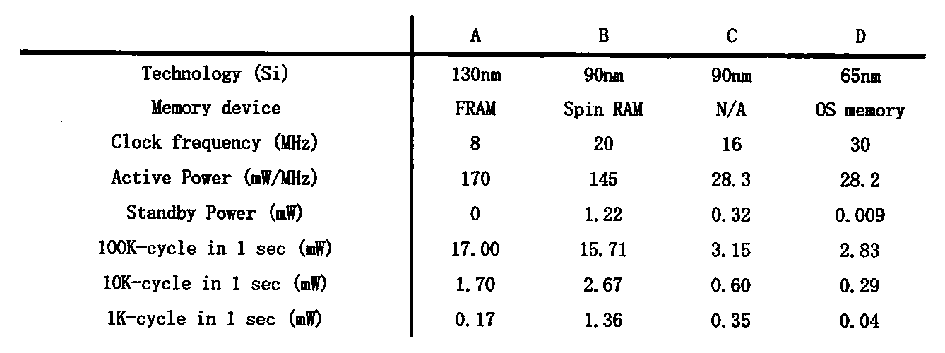
ADDR 信号、BGL 配線、BL 配線、BLB 配線、BW 信号、C0 容量素子、C1 容量素子、C2 容量素子、C21 容量素子、C23 容量素子、C22 容量素子、C24 容量素子、CE 信号、CLK 信号、DB1 データ、DB2 データ、GW 信号、L1 層、L2 層、L3 層、L4 層、LBL 配線、LBLB配線、M1 トランジスタ、M21 トランジスタ、M24 トランジスタ、M31 トランジスタ、M34 トランジスタ、NWL 配線、NWL_0 配線、NWL_1 配線、OS1 トランジスタ、PCL 配線、PON1 信号、PON2 信号、RDA 信号、VCS 配線、VDDM 配線、VHH 配線、VLL 配線、VPC 配線、WDA 信号、WL 配線、t1 時刻、t2 時刻、t3 時刻、t4 時刻、t5 時刻、t6 時刻、t7 時刻、t8 時刻、Tac1 トランジスタ、Tac2 トランジスタ、Tdr1 トランジスタ、Teq1 トランジスタ、Tld1 トランジスタ、Tld2 トランジスタ、Tpc1 トランジスタ、Tpc2 トランジスタ、Tr1 トランジスタ、Tr2 トランジスタ、Tr3 トランジスタ、Tr4 トランジスタ、10 SMC、20NVM、21 NVM、30 LPC、100 記憶装置、110 メモリセルアレイ、110A メモリセルアレイ、110B メモリセルアレイ、111 周辺回路、112 コントロール回路、115 周辺回路、121 行デコーダ、122 列デコータ、123 行ドライバ、124 列ドライバ、125 入力回路、126 出力回路、127 電圧生成回路、127a 電圧生成回路、127b 電圧生成回路、128 電圧保持回路、130メモリセル、141 PSW、142 PSW、200a トランジスタ、200b トランジスタ、200c トランジスタ、200d トランジスタ、205 導電体、205a導電体、205b 導電体、214 絶縁体、216 絶縁体、220 絶縁体、222 絶縁体、224 絶縁体、230 酸化物半導体、230a 酸化物半導体、230b 酸化物半導体、230c 酸化物半導体、240a 導電体、240b 導電体、241 絶縁体、250 絶縁体、260 導電体、280 絶縁体、282 絶縁体、300 基板、301 素子分離層、302 絶縁体、303 絶縁体、304 絶縁体、305 絶縁体、310 プラグ、311 プラグ、312 プラグ、313 プラグ、320 配線、321 配線、322 導電体、323 導電体、324 絶縁体、331 プラグ、332 プラグ、333 プラグ、334 プラグ、341 配線、342 配線、343配線、351 ウェル、352 チャネル形成領域、353 不純物領域、354 不純物領域、355 導電性領域、356 導電性領域、357 ゲート電極、358 ゲート絶縁体、361 ウェル、362 チャネル形成領域、363 高濃度不純物領域、364 高濃度不純物領域、365 導電性領域、366 導電性領域、367 ゲート電極、368ゲート絶縁体、369 側壁絶縁層、370 側壁絶縁層、371 低濃度不純物領域、372 低濃度不純物領域、611 基板、612 回路領域、613 分離領域、614 分離線、615 チップ、650 電子部品、652 プリント基板、653 半導体装置、654 基板、655 リード、700 腕時計型端末、701 筐体、702 リュウズ、703 表示部、704 ベルト、705 検知部、710 携帯電話機、711 筐体、712 マイク、713 外部接続ポート、714 操作ボタン、716 表示部、717 スピーカ、720 ノート型パーソナルコンピュータ、721 筐体、722 表示部、723 キーボード、724 ポインティングデバイス、730 ゴーグル型ディスプレイ、731 装着部、732 筐体、735 ケーブル、736 バッテリ、737 表示部、740 ビデオカメラ、741 筐体、742 筐体、743 表示部、744 操作キー、745 レンズ、746 接続部、750 自動車、751 車体、752 車輪、753 ダッシュボード、754 ライト、1300 CPU、1302 パワーコントローラ、1303 パワースイッチ、1304 キャッシュメモリ、1305 バスインターフェース、1306 デバッグインターフェース、1307 制御装置、1308 プログラムカウンタ、1309 パイプラインレジスタ、1310 パイプラインレジスタ、1311ALU、1312 レジスタファイル、1330 CPUコア、1331 PMU、1332周辺回路、1333 データバス、1400 RFIC、1404 アンテナ、1405 整流回路、1406 定電圧回路、1407 復調回路、1408 変調回路、1409 論理回路、1410 RAM、1411 ROM、1412 バッテリ、1420 通信器、1421 アンテナ、1422 無線信号
Claims (8)
- 複数のメモリセルと、
プリチャージ回路と、
ラッチ回路と、
第1ビット線と第2ビット線とでなるビット線対と、
第1ローカルビット線と第2ローカルビット線とでなるローカルビット線対と、
第1トランジスタと、
第2トランジスタと、を有し、
前記第1トランジスタは前記第1ビット線と前記第1ローカルビット線との導通状態を制御する機能を有し、
前記第2トランジスタは前記第2ビット線と前記第2ローカルビット線との導通状態を制御する機能を有し、
前記複数のメモリセルは、それぞれ、第3トランジスタ、第4トランジスタ、第1容量素子および第2容量素子を有し、
前記第3トランジスタは前記第1ローカルビット線と前記第1容量素子との導通状態を制御する機能を有し、
前記第4トランジスタは前記第2ローカルビット線と前記第2容量素子との導通状態を制御する機能を有し、
前記プリチャージ回路は前記ローカルビット線対にプリチャージ電圧を供給する機能を有し、
前記ラッチ回路は前記ローカルビット線対と電気的に接続され、
前記第1トランジスタ、前記第2トランジスタ、前記第3トランジスタおよび前記第4トランジスタが非導通のときに、前記プリチャージ電圧と、低電源電圧または高電源電圧の一方が前記ラッチ回路に供給されることを特徴とする記憶装置。 - 請求項1において、
前記第3トランジスタはチャネル形成領域に酸化物半導体を有し、
前記第4トランジスタはチャネル形成領域に酸化物半導体を有することを特徴とする記憶装置。 - 請求項2において、
前記複数のメモリセルは前記プリチャージ回路または前記ラッチ回路の上に設けられていることを特徴とする記憶装置。 - 複数のメモリセルと、
プリチャージ回路と、
ラッチ回路と、
第1ビット線と第2ビット線とでなるビット線対と、
第1ローカルビット線と第2ローカルビット線とでなるローカルビット線対と、
第1トランジスタと、
第2トランジスタと、を有し、
前記第1トランジスタは前記第1ビット線と前記第1ローカルビット線との導通状態を制御する機能を有し、
前記第2トランジスタは前記第2ビット線と前記第2ローカルビット線との導通状態を制御する機能を有し、
前記複数のメモリセルは、それぞれ、第1メモリセルと第2メモリセルに分類され、
前記第1メモリセルは、第3トランジスタおよび第1容量素子を有し、
前記第2メモリセルは、第4トランジスタおよび第2容量素子を有し、
前記第3トランジスタは前記第1ローカルビット線と前記第1容量素子との導通状態を制御する機能を有し、
前記第4トランジスタは前記第2ローカルビット線と前記第2容量素子との導通状態を制御する機能を有し、
前記プリチャージ回路は前記ローカルビット線対にプリチャージ電圧を供給する機能を有し、
前記ラッチ回路は前記ローカルビット線対と電気的に接続され、
前記第1トランジスタ、前記第2トランジスタ、前記第3トランジスタおよび前記第4トランジスタが非導通のときに、前記プリチャージ電圧と、低電源電圧または高電源電圧の一方が前記ラッチ回路に供給されることを特徴とする記憶装置。 - 請求項4において、
前記第3トランジスタはチャネル形成領域に酸化物半導体を有し、
前記第4トランジスタはチャネル形成領域に酸化物半導体を有することを特徴とする記憶装置。 - 請求項5において、
前記複数のメモリセルは前記プリチャージ回路または前記ラッチ回路の上に設けられていることを特徴とする記憶装置。 - 請求項1乃至請求項6のいずれか一項に記載の前記記憶装置を複数有し、
分離領域を有する半導体ウエハ。 - 請求項1乃至請求項6のいずれか一項に記載の前記記憶装置と
バッテリと、を有する電子機器。
Priority Applications (5)
| Application Number | Priority Date | Filing Date | Title |
|---|---|---|---|
| US16/079,355 US10622059B2 (en) | 2016-03-18 | 2017-03-06 | Oxide semiconductor based memory device |
| JP2018505546A JPWO2017158465A1 (ja) | 2016-03-18 | 2017-03-06 | 記憶装置 |
| US16/832,289 US11094373B2 (en) | 2016-03-18 | 2020-03-27 | Oxide semiconductor based memory device |
| JP2021201923A JP2022033961A (ja) | 2016-03-18 | 2021-12-13 | 記憶装置及び電子機器 |
| JP2023115615A JP7682956B2 (ja) | 2016-03-18 | 2023-07-14 | 記憶装置 |
Applications Claiming Priority (4)
| Application Number | Priority Date | Filing Date | Title |
|---|---|---|---|
| JP2016-055513 | 2016-03-18 | ||
| JP2016055513 | 2016-03-18 | ||
| JP2016079484 | 2016-04-12 | ||
| JP2016-079484 | 2016-04-12 |
Related Child Applications (2)
| Application Number | Title | Priority Date | Filing Date |
|---|---|---|---|
| US16/079,355 A-371-Of-International US10622059B2 (en) | 2016-03-18 | 2017-03-06 | Oxide semiconductor based memory device |
| US16/832,289 Continuation US11094373B2 (en) | 2016-03-18 | 2020-03-27 | Oxide semiconductor based memory device |
Publications (1)
| Publication Number | Publication Date |
|---|---|
| WO2017158465A1 true WO2017158465A1 (ja) | 2017-09-21 |
Family
ID=59850252
Family Applications (1)
| Application Number | Title | Priority Date | Filing Date |
|---|---|---|---|
| PCT/IB2017/051279 Ceased WO2017158465A1 (ja) | 2016-03-18 | 2017-03-06 | 記憶装置 |
Country Status (3)
| Country | Link |
|---|---|
| US (2) | US10622059B2 (ja) |
| JP (3) | JPWO2017158465A1 (ja) |
| WO (1) | WO2017158465A1 (ja) |
Cited By (8)
| Publication number | Priority date | Publication date | Assignee | Title |
|---|---|---|---|---|
| US10210915B2 (en) | 2016-06-10 | 2019-02-19 | Semiconductor Energy Laboratory Co., Ltd. | Memory device and semiconductor device including the same |
| WO2019171205A1 (ja) * | 2018-03-06 | 2019-09-12 | 株式会社半導体エネルギー研究所 | 積層体、及び半導体装置 |
| WO2020136464A1 (ja) * | 2018-12-28 | 2020-07-02 | 株式会社半導体エネルギー研究所 | メモリデバイス、当該メモリデバイスを有する半導体装置 |
| WO2020245697A1 (ja) * | 2019-06-07 | 2020-12-10 | 株式会社半導体エネルギー研究所 | 半導体装置 |
| JPWO2019130144A1 (ja) * | 2017-12-27 | 2021-01-14 | 株式会社半導体エネルギー研究所 | 記憶装置 |
| WO2021044821A1 (ja) * | 2019-09-02 | 2021-03-11 | ソニー株式会社 | 演算装置及び積和演算システム |
| JPWO2022049448A1 (ja) * | 2020-09-06 | 2022-03-10 | ||
| WO2024074936A1 (ja) * | 2022-10-04 | 2024-04-11 | 株式会社半導体エネルギー研究所 | 半導体装置 |
Families Citing this family (11)
| Publication number | Priority date | Publication date | Assignee | Title |
|---|---|---|---|---|
| WO2019049013A1 (ja) | 2017-09-06 | 2019-03-14 | 株式会社半導体エネルギー研究所 | 半導体装置 |
| US10290348B1 (en) * | 2018-02-12 | 2019-05-14 | Sandisk Technologies Llc | Write-once read-many amorphous chalcogenide-based memory |
| CN120035137A (zh) | 2018-02-23 | 2025-05-23 | 株式会社半导体能源研究所 | 存储装置及其工作方法 |
| TW202431270A (zh) | 2019-03-29 | 2024-08-01 | 日商半導體能源研究所股份有限公司 | 半導體裝置 |
| KR102640960B1 (ko) * | 2019-06-04 | 2024-02-27 | 에스케이하이닉스 주식회사 | 노이즈 증폭 회로 및 이를 포함하는 메모리 장치 |
| JP2021108307A (ja) * | 2019-12-27 | 2021-07-29 | キオクシア株式会社 | 半導体記憶装置 |
| DE102021109480A1 (de) | 2020-12-14 | 2022-06-15 | Taiwan Semiconductor Manufacturing Co., Ltd. | Speichervorrichtung |
| CN114388018B (zh) * | 2020-12-14 | 2025-09-19 | 台湾积体电路制造股份有限公司 | 存储装置 |
| US11380387B1 (en) * | 2021-03-23 | 2022-07-05 | Micron Technology, Inc. | Multiplexor for a semiconductor device |
| US20260107442A1 (en) * | 2022-10-07 | 2026-04-16 | Semiconductor Energy Laboratory Co., Ltd. | Semiconductor device and arithmetic device |
| JPWO2025032477A1 (ja) * | 2023-08-10 | 2025-02-13 |
Citations (5)
| Publication number | Priority date | Publication date | Assignee | Title |
|---|---|---|---|---|
| WO2003052829A1 (fr) * | 2001-12-14 | 2003-06-26 | Hitachi, Ltd. | Dispositif semi-conducteur et procede de fabrication correspondant |
| JP2013168631A (ja) * | 2011-12-09 | 2013-08-29 | Semiconductor Energy Lab Co Ltd | 記憶装置 |
| JP2014063557A (ja) * | 2012-02-24 | 2014-04-10 | Semiconductor Energy Lab Co Ltd | 記憶装置及び半導体装置 |
| JP2016033842A (ja) * | 2014-07-31 | 2016-03-10 | 株式会社フローディア | 不揮発性sramメモリセル、および不揮発性半導体記憶装置 |
| US20160078938A1 (en) * | 2014-09-15 | 2016-03-17 | NEO Semiconductor, Inc. | Method and apparatus for providing multi-page read and write using sram and nonvolatile memory devices |
Family Cites Families (30)
| Publication number | Priority date | Publication date | Assignee | Title |
|---|---|---|---|---|
| US5357460A (en) * | 1991-05-28 | 1994-10-18 | Sharp Kabushiki Kaisha | Semiconductor memory device having two transistors and at least one ferroelectric film capacitor |
| US5430671A (en) * | 1993-04-09 | 1995-07-04 | Matsushita Electric Industrial Co., Ltd. | Semiconductor memory device |
| JPH10112188A (ja) * | 1996-10-03 | 1998-04-28 | Hitachi Ltd | 半導体集積回路装置 |
| JP4353393B2 (ja) * | 2001-06-05 | 2009-10-28 | 株式会社ルネサステクノロジ | 半導体集積回路装置 |
| JP2004023062A (ja) * | 2002-06-20 | 2004-01-22 | Nec Electronics Corp | 半導体装置とその製造方法 |
| KR101973212B1 (ko) * | 2010-11-05 | 2019-04-26 | 가부시키가이샤 한도오따이 에네루기 켄큐쇼 | 반도체 장치 |
| US8421071B2 (en) * | 2011-01-13 | 2013-04-16 | Semiconductor Energy Laboratory Co., Ltd. | Memory device |
| TWI616873B (zh) | 2011-05-20 | 2018-03-01 | 半導體能源研究所股份有限公司 | 儲存裝置及信號處理電路 |
| JP5886496B2 (ja) | 2011-05-20 | 2016-03-16 | 株式会社半導体エネルギー研究所 | 半導体装置 |
| TWI573136B (zh) | 2011-05-20 | 2017-03-01 | 半導體能源研究所股份有限公司 | 儲存裝置及信號處理電路 |
| JP6105266B2 (ja) | 2011-12-15 | 2017-03-29 | 株式会社半導体エネルギー研究所 | 記憶装置 |
| JP2013190893A (ja) | 2012-03-13 | 2013-09-26 | Rohm Co Ltd | マルチタスク処理装置 |
| US9001549B2 (en) | 2012-05-11 | 2015-04-07 | Semiconductor Energy Laboratory Co., Ltd. | Semiconductor device |
| JP5312715B1 (ja) * | 2012-05-18 | 2013-10-09 | 独立行政法人科学技術振興機構 | 双安定回路と不揮発性素子とを備える記憶回路 |
| TWI620323B (zh) | 2012-11-16 | 2018-04-01 | 半導體能源研究所股份有限公司 | 半導體裝置 |
| TWI618058B (zh) | 2013-05-16 | 2018-03-11 | 半導體能源研究所股份有限公司 | 半導體裝置 |
| JP6457239B2 (ja) * | 2013-10-31 | 2019-01-23 | 株式会社半導体エネルギー研究所 | 半導体装置 |
| US9716100B2 (en) * | 2014-03-14 | 2017-07-25 | Semiconductor Energy Laboratory Co., Ltd. | Semiconductor device, method for driving semiconductor device, and electronic device |
| KR102398965B1 (ko) * | 2014-03-20 | 2022-05-17 | 가부시키가이샤 한도오따이 에네루기 켄큐쇼 | 반도체 장치, 전자 부품, 및 전자 기기 |
| US20150294991A1 (en) | 2014-04-10 | 2015-10-15 | Semiconductor Energy Laboratory Co., Ltd. | Semiconductor device, electronic component, and electronic device |
| TWI767772B (zh) | 2014-04-10 | 2022-06-11 | 日商半導體能源研究所股份有限公司 | 記憶體裝置及半導體裝置 |
| JP6635670B2 (ja) * | 2014-04-11 | 2020-01-29 | 株式会社半導体エネルギー研究所 | 半導体装置 |
| WO2015170220A1 (en) * | 2014-05-09 | 2015-11-12 | Semiconductor Energy Laboratory Co., Ltd. | Memory device and electronic device |
| JP2016015475A (ja) | 2014-06-13 | 2016-01-28 | 株式会社半導体エネルギー研究所 | 半導体装置、及び電子機器 |
| KR20170023813A (ko) | 2014-06-20 | 2017-03-06 | 가부시키가이샤 한도오따이 에네루기 켄큐쇼 | 반도체 장치 |
| KR20170069207A (ko) * | 2014-10-10 | 2017-06-20 | 가부시키가이샤 한도오따이 에네루기 켄큐쇼 | 반도체 장치, 회로 기판, 및 전자 기기 |
| US10236884B2 (en) | 2015-02-09 | 2019-03-19 | Semiconductor Energy Laboratory Co., Ltd. | Word line driver comprising NAND circuit |
| TWI693719B (zh) * | 2015-05-11 | 2020-05-11 | 日商半導體能源研究所股份有限公司 | 半導體裝置的製造方法 |
| WO2016181256A1 (ja) | 2015-05-12 | 2016-11-17 | 株式会社半導体エネルギー研究所 | 半導体装置、電子部品および電子機器 |
| US10210915B2 (en) | 2016-06-10 | 2019-02-19 | Semiconductor Energy Laboratory Co., Ltd. | Memory device and semiconductor device including the same |
-
2017
- 2017-03-06 JP JP2018505546A patent/JPWO2017158465A1/ja not_active Withdrawn
- 2017-03-06 WO PCT/IB2017/051279 patent/WO2017158465A1/ja not_active Ceased
- 2017-03-06 US US16/079,355 patent/US10622059B2/en active Active
-
2020
- 2020-03-27 US US16/832,289 patent/US11094373B2/en not_active Expired - Fee Related
-
2021
- 2021-12-13 JP JP2021201923A patent/JP2022033961A/ja not_active Withdrawn
-
2023
- 2023-07-14 JP JP2023115615A patent/JP7682956B2/ja active Active
Patent Citations (5)
| Publication number | Priority date | Publication date | Assignee | Title |
|---|---|---|---|---|
| WO2003052829A1 (fr) * | 2001-12-14 | 2003-06-26 | Hitachi, Ltd. | Dispositif semi-conducteur et procede de fabrication correspondant |
| JP2013168631A (ja) * | 2011-12-09 | 2013-08-29 | Semiconductor Energy Lab Co Ltd | 記憶装置 |
| JP2014063557A (ja) * | 2012-02-24 | 2014-04-10 | Semiconductor Energy Lab Co Ltd | 記憶装置及び半導体装置 |
| JP2016033842A (ja) * | 2014-07-31 | 2016-03-10 | 株式会社フローディア | 不揮発性sramメモリセル、および不揮発性半導体記憶装置 |
| US20160078938A1 (en) * | 2014-09-15 | 2016-03-17 | NEO Semiconductor, Inc. | Method and apparatus for providing multi-page read and write using sram and nonvolatile memory devices |
Cited By (24)
| Publication number | Priority date | Publication date | Assignee | Title |
|---|---|---|---|---|
| US10210915B2 (en) | 2016-06-10 | 2019-02-19 | Semiconductor Energy Laboratory Co., Ltd. | Memory device and semiconductor device including the same |
| JPWO2019130144A1 (ja) * | 2017-12-27 | 2021-01-14 | 株式会社半導体エネルギー研究所 | 記憶装置 |
| JP7142029B2 (ja) | 2017-12-27 | 2022-09-26 | 株式会社半導体エネルギー研究所 | 記憶装置 |
| JP7142081B2 (ja) | 2018-03-06 | 2022-09-26 | 株式会社半導体エネルギー研究所 | 積層体、及び半導体装置 |
| JPWO2019171205A1 (ja) * | 2018-03-06 | 2021-02-25 | 株式会社半導体エネルギー研究所 | 積層体、及び半導体装置 |
| WO2019171205A1 (ja) * | 2018-03-06 | 2019-09-12 | 株式会社半導体エネルギー研究所 | 積層体、及び半導体装置 |
| US11387343B2 (en) | 2018-03-06 | 2022-07-12 | Semiconductor Energy Laboratory Co., Ltd. | Stack and semiconductor device |
| JP2024164220A (ja) * | 2018-12-28 | 2024-11-26 | 株式会社半導体エネルギー研究所 | メモリデバイス |
| US12063770B2 (en) | 2018-12-28 | 2024-08-13 | Semiconductor Energy Laboratory Co., Ltd. | Memory device and semiconductor device including the memory device |
| KR20210108967A (ko) * | 2018-12-28 | 2021-09-03 | 가부시키가이샤 한도오따이 에네루기 켄큐쇼 | 메모리 디바이스, 상기 메모리 디바이스를 갖는 반도체 장치 |
| KR102923216B1 (ko) * | 2018-12-28 | 2026-02-04 | 가부시키가이샤 한도오따이 에네루기 켄큐쇼 | 메모리 디바이스, 상기 메모리 디바이스를 갖는 반도체 장치 |
| JPWO2020136464A1 (ja) * | 2018-12-28 | 2020-07-02 | ||
| WO2020136464A1 (ja) * | 2018-12-28 | 2020-07-02 | 株式会社半導体エネルギー研究所 | メモリデバイス、当該メモリデバイスを有する半導体装置 |
| JP7789867B2 (ja) | 2018-12-28 | 2025-12-22 | 株式会社半導体エネルギー研究所 | メモリデバイス |
| TWI861028B (zh) * | 2018-12-28 | 2024-11-11 | 日商半導體能源研究所股份有限公司 | 記憶體件及包括該記憶體件的半導體裝置 |
| JP7524175B2 (ja) | 2019-06-07 | 2024-07-29 | 株式会社半導体エネルギー研究所 | 半導体装置 |
| US12015012B2 (en) | 2019-06-07 | 2024-06-18 | Semiconductor Energy Laboratory Co., Ltd. | Semiconductor device |
| WO2020245697A1 (ja) * | 2019-06-07 | 2020-12-10 | 株式会社半導体エネルギー研究所 | 半導体装置 |
| US12381187B2 (en) | 2019-06-07 | 2025-08-05 | Semiconductor Energy Laboratory Co., Ltd. | Semiconductor device |
| JPWO2020245697A1 (ja) * | 2019-06-07 | 2020-12-10 | ||
| WO2021044821A1 (ja) * | 2019-09-02 | 2021-03-11 | ソニー株式会社 | 演算装置及び積和演算システム |
| JP7711071B2 (ja) | 2020-09-06 | 2025-07-22 | 株式会社半導体エネルギー研究所 | 半導体装置、及び電子機器 |
| JPWO2022049448A1 (ja) * | 2020-09-06 | 2022-03-10 | ||
| WO2024074936A1 (ja) * | 2022-10-04 | 2024-04-11 | 株式会社半導体エネルギー研究所 | 半導体装置 |
Also Published As
| Publication number | Publication date |
|---|---|
| US10622059B2 (en) | 2020-04-14 |
| JP2023133353A (ja) | 2023-09-22 |
| US11094373B2 (en) | 2021-08-17 |
| US20200342935A1 (en) | 2020-10-29 |
| JP7682956B2 (ja) | 2025-05-26 |
| JP2022033961A (ja) | 2022-03-02 |
| US20190057734A1 (en) | 2019-02-21 |
| JPWO2017158465A1 (ja) | 2019-02-14 |
Similar Documents
| Publication | Publication Date | Title |
|---|---|---|
| JP7682956B2 (ja) | 記憶装置 | |
| JP7032510B2 (ja) | 半導体装置 | |
| JP6869021B2 (ja) | 半導体装置 | |
| JP6962755B2 (ja) | 半導体装置 | |
| US10002648B2 (en) | Memory device, semiconductor device, and electronic device | |
| JP2017139460A (ja) | マイクロコントローラシステム | |
| JP6827328B2 (ja) | 半導体装置及び電子機器 | |
| US11922987B2 (en) | Storage device, electronic component, and electronic device | |
| JP7628643B2 (ja) | 半導体装置 | |
| KR20170023813A (ko) | 반도체 장치 | |
| US10304488B2 (en) | Semiconductor device comprising memory cell | |
| JP2022116138A (ja) | 記憶装置 | |
| JPWO2016181256A1 (ja) | 半導体装置、電子部品および電子機器 | |
| JP2017182867A (ja) | 半導体装置、ドライバic、コンピュータ及び電子機器 | |
| WO2020245688A1 (ja) | 半導体装置、半導体ウエハ、及び電子機器 |
Legal Events
| Date | Code | Title | Description |
|---|---|---|---|
| WWE | Wipo information: entry into national phase |
Ref document number: 2018505546 Country of ref document: JP |
|
| NENP | Non-entry into the national phase |
Ref country code: DE |
|
| 121 | Ep: the epo has been informed by wipo that ep was designated in this application |
Ref document number: 17765932 Country of ref document: EP Kind code of ref document: A1 |
|
| 122 | Ep: pct application non-entry in european phase |
Ref document number: 17765932 Country of ref document: EP Kind code of ref document: A1 |