WO2017138255A1 - 導電性接着フィルムおよびこれを用いたダイシング・ダイボンディングフィルム - Google Patents
導電性接着フィルムおよびこれを用いたダイシング・ダイボンディングフィルム Download PDFInfo
- Publication number
- WO2017138255A1 WO2017138255A1 PCT/JP2016/087661 JP2016087661W WO2017138255A1 WO 2017138255 A1 WO2017138255 A1 WO 2017138255A1 JP 2016087661 W JP2016087661 W JP 2016087661W WO 2017138255 A1 WO2017138255 A1 WO 2017138255A1
- Authority
- WO
- WIPO (PCT)
- Prior art keywords
- conductive adhesive
- group
- adhesive film
- metal particles
- resin
- Prior art date
- Legal status (The legal status is an assumption and is not a legal conclusion. Google has not performed a legal analysis and makes no representation as to the accuracy of the status listed.)
- Ceased
Links
Images

Classifications
-
- C—CHEMISTRY; METALLURGY
- C09—DYES; PAINTS; POLISHES; NATURAL RESINS; ADHESIVES; COMPOSITIONS NOT OTHERWISE PROVIDED FOR; APPLICATIONS OF MATERIALS NOT OTHERWISE PROVIDED FOR
- C09J—ADHESIVES; NON-MECHANICAL ASPECTS OF ADHESIVE PROCESSES IN GENERAL; ADHESIVE PROCESSES NOT PROVIDED FOR ELSEWHERE; USE OF MATERIALS AS ADHESIVES
- C09J7/00—Adhesives in the form of films or foils
- C09J7/10—Adhesives in the form of films or foils without carriers
-
- C—CHEMISTRY; METALLURGY
- C09—DYES; PAINTS; POLISHES; NATURAL RESINS; ADHESIVES; COMPOSITIONS NOT OTHERWISE PROVIDED FOR; APPLICATIONS OF MATERIALS NOT OTHERWISE PROVIDED FOR
- C09J—ADHESIVES; NON-MECHANICAL ASPECTS OF ADHESIVE PROCESSES IN GENERAL; ADHESIVE PROCESSES NOT PROVIDED FOR ELSEWHERE; USE OF MATERIALS AS ADHESIVES
- C09J11/00—Features of adhesives not provided for in group C09J9/00, e.g. additives
- C09J11/02—Non-macromolecular additives
- C09J11/04—Non-macromolecular additives inorganic
-
- C—CHEMISTRY; METALLURGY
- C09—DYES; PAINTS; POLISHES; NATURAL RESINS; ADHESIVES; COMPOSITIONS NOT OTHERWISE PROVIDED FOR; APPLICATIONS OF MATERIALS NOT OTHERWISE PROVIDED FOR
- C09J—ADHESIVES; NON-MECHANICAL ASPECTS OF ADHESIVE PROCESSES IN GENERAL; ADHESIVE PROCESSES NOT PROVIDED FOR ELSEWHERE; USE OF MATERIALS AS ADHESIVES
- C09J11/00—Features of adhesives not provided for in group C09J9/00, e.g. additives
- C09J11/02—Non-macromolecular additives
- C09J11/06—Non-macromolecular additives organic
-
- C—CHEMISTRY; METALLURGY
- C09—DYES; PAINTS; POLISHES; NATURAL RESINS; ADHESIVES; COMPOSITIONS NOT OTHERWISE PROVIDED FOR; APPLICATIONS OF MATERIALS NOT OTHERWISE PROVIDED FOR
- C09J—ADHESIVES; NON-MECHANICAL ASPECTS OF ADHESIVE PROCESSES IN GENERAL; ADHESIVE PROCESSES NOT PROVIDED FOR ELSEWHERE; USE OF MATERIALS AS ADHESIVES
- C09J157/00—Adhesives based on unspecified polymers obtained by reactions only involving carbon-to-carbon unsaturated bonds
- C09J157/06—Homopolymers or copolymers containing elements other than carbon and hydrogen
- C09J157/12—Homopolymers or copolymers containing elements other than carbon and hydrogen containing nitrogen atoms
-
- C—CHEMISTRY; METALLURGY
- C09—DYES; PAINTS; POLISHES; NATURAL RESINS; ADHESIVES; COMPOSITIONS NOT OTHERWISE PROVIDED FOR; APPLICATIONS OF MATERIALS NOT OTHERWISE PROVIDED FOR
- C09J—ADHESIVES; NON-MECHANICAL ASPECTS OF ADHESIVE PROCESSES IN GENERAL; ADHESIVE PROCESSES NOT PROVIDED FOR ELSEWHERE; USE OF MATERIALS AS ADHESIVES
- C09J163/00—Adhesives based on epoxy resins; Adhesives based on derivatives of epoxy resins
-
- C—CHEMISTRY; METALLURGY
- C09—DYES; PAINTS; POLISHES; NATURAL RESINS; ADHESIVES; COMPOSITIONS NOT OTHERWISE PROVIDED FOR; APPLICATIONS OF MATERIALS NOT OTHERWISE PROVIDED FOR
- C09J—ADHESIVES; NON-MECHANICAL ASPECTS OF ADHESIVE PROCESSES IN GENERAL; ADHESIVE PROCESSES NOT PROVIDED FOR ELSEWHERE; USE OF MATERIALS AS ADHESIVES
- C09J201/00—Adhesives based on unspecified macromolecular compounds
- C09J201/02—Adhesives based on unspecified macromolecular compounds characterised by the presence of specified groups, e.g. terminal or pendant functional groups
- C09J201/025—Adhesives based on unspecified macromolecular compounds characterised by the presence of specified groups, e.g. terminal or pendant functional groups containing nitrogen atoms
-
- C—CHEMISTRY; METALLURGY
- C09—DYES; PAINTS; POLISHES; NATURAL RESINS; ADHESIVES; COMPOSITIONS NOT OTHERWISE PROVIDED FOR; APPLICATIONS OF MATERIALS NOT OTHERWISE PROVIDED FOR
- C09J—ADHESIVES; NON-MECHANICAL ASPECTS OF ADHESIVE PROCESSES IN GENERAL; ADHESIVE PROCESSES NOT PROVIDED FOR ELSEWHERE; USE OF MATERIALS AS ADHESIVES
- C09J7/00—Adhesives in the form of films or foils
- C09J7/30—Adhesives in the form of films or foils characterised by the adhesive composition
- C09J7/35—Heat-activated
-
- C—CHEMISTRY; METALLURGY
- C09—DYES; PAINTS; POLISHES; NATURAL RESINS; ADHESIVES; COMPOSITIONS NOT OTHERWISE PROVIDED FOR; APPLICATIONS OF MATERIALS NOT OTHERWISE PROVIDED FOR
- C09J—ADHESIVES; NON-MECHANICAL ASPECTS OF ADHESIVE PROCESSES IN GENERAL; ADHESIVE PROCESSES NOT PROVIDED FOR ELSEWHERE; USE OF MATERIALS AS ADHESIVES
- C09J9/00—Adhesives characterised by their physical nature or the effects produced, e.g. glue sticks
- C09J9/02—Electrically-conducting adhesives
-
- H—ELECTRICITY
- H01—ELECTRIC ELEMENTS
- H01B—CABLES; CONDUCTORS; INSULATORS; SELECTION OF MATERIALS FOR THEIR CONDUCTIVE, INSULATING OR DIELECTRIC PROPERTIES
- H01B1/00—Conductors or conductive bodies characterised by the conductive materials; Selection of materials as conductors
- H01B1/20—Conductive material dispersed in non-conductive organic material
- H01B1/22—Conductive material dispersed in non-conductive organic material the conductive material comprising metals or alloys
-
- H—ELECTRICITY
- H01—ELECTRIC ELEMENTS
- H01B—CABLES; CONDUCTORS; INSULATORS; SELECTION OF MATERIALS FOR THEIR CONDUCTIVE, INSULATING OR DIELECTRIC PROPERTIES
- H01B5/00—Non-insulated conductors or conductive bodies characterised by their form
- H01B5/14—Non-insulated conductors or conductive bodies characterised by their form comprising conductive layers or films on insulating-supports
-
- H—ELECTRICITY
- H10—SEMICONDUCTOR DEVICES; ELECTRIC SOLID-STATE DEVICES NOT OTHERWISE PROVIDED FOR
- H10P—GENERIC PROCESSES OR APPARATUS FOR THE MANUFACTURE OR TREATMENT OF DEVICES COVERED BY CLASS H10
- H10P72/00—Handling or holding of wafers, substrates or devices during manufacture or treatment thereof
- H10P72/70—Handling or holding of wafers, substrates or devices during manufacture or treatment thereof for supporting or gripping
- H10P72/74—Handling or holding of wafers, substrates or devices during manufacture or treatment thereof for supporting or gripping using temporarily an auxiliary support
- H10P72/7402—Wafer tapes, e.g. grinding or dicing support tapes
-
- H—ELECTRICITY
- H10—SEMICONDUCTOR DEVICES; ELECTRIC SOLID-STATE DEVICES NOT OTHERWISE PROVIDED FOR
- H10W—GENERIC PACKAGES, INTERCONNECTIONS, CONNECTORS OR OTHER CONSTRUCTIONAL DETAILS OF DEVICES COVERED BY CLASS H10
- H10W72/00—Interconnections or connectors in packages
- H10W72/30—Die-attach connectors
-
- H—ELECTRICITY
- H10—SEMICONDUCTOR DEVICES; ELECTRIC SOLID-STATE DEVICES NOT OTHERWISE PROVIDED FOR
- H10W—GENERIC PACKAGES, INTERCONNECTIONS, CONNECTORS OR OTHER CONSTRUCTIONAL DETAILS OF DEVICES COVERED BY CLASS H10
- H10W72/00—Interconnections or connectors in packages
- H10W72/851—Dispositions of multiple connectors or interconnections
-
- H—ELECTRICITY
- H10—SEMICONDUCTOR DEVICES; ELECTRIC SOLID-STATE DEVICES NOT OTHERWISE PROVIDED FOR
- H10W—GENERIC PACKAGES, INTERCONNECTIONS, CONNECTORS OR OTHER CONSTRUCTIONAL DETAILS OF DEVICES COVERED BY CLASS H10
- H10W99/00—Subject matter not provided for in other groups of this subclass
-
- C—CHEMISTRY; METALLURGY
- C08—ORGANIC MACROMOLECULAR COMPOUNDS; THEIR PREPARATION OR CHEMICAL WORKING-UP; COMPOSITIONS BASED THEREON
- C08K—Use of inorganic or non-macromolecular organic substances as compounding ingredients
- C08K3/00—Use of inorganic substances as compounding ingredients
- C08K3/02—Elements
- C08K3/08—Metals
-
- C—CHEMISTRY; METALLURGY
- C08—ORGANIC MACROMOLECULAR COMPOUNDS; THEIR PREPARATION OR CHEMICAL WORKING-UP; COMPOSITIONS BASED THEREON
- C08K—Use of inorganic or non-macromolecular organic substances as compounding ingredients
- C08K5/00—Use of organic ingredients
- C08K5/36—Sulfur-, selenium-, or tellurium-containing compounds
- C08K5/37—Thiols
- C08K5/372—Sulfides, e.g. R-(S)x-R'
-
- C—CHEMISTRY; METALLURGY
- C08—ORGANIC MACROMOLECULAR COMPOUNDS; THEIR PREPARATION OR CHEMICAL WORKING-UP; COMPOSITIONS BASED THEREON
- C08K—Use of inorganic or non-macromolecular organic substances as compounding ingredients
- C08K5/00—Use of organic ingredients
- C08K5/49—Phosphorus-containing compounds
- C08K5/50—Phosphorus bound to carbon only
-
- C—CHEMISTRY; METALLURGY
- C09—DYES; PAINTS; POLISHES; NATURAL RESINS; ADHESIVES; COMPOSITIONS NOT OTHERWISE PROVIDED FOR; APPLICATIONS OF MATERIALS NOT OTHERWISE PROVIDED FOR
- C09J—ADHESIVES; NON-MECHANICAL ASPECTS OF ADHESIVE PROCESSES IN GENERAL; ADHESIVE PROCESSES NOT PROVIDED FOR ELSEWHERE; USE OF MATERIALS AS ADHESIVES
- C09J2203/00—Applications of adhesives in processes or use of adhesives in the form of films or foils
- C09J2203/326—Applications of adhesives in processes or use of adhesives in the form of films or foils for bonding electronic components such as wafers, chips or semiconductors
-
- C—CHEMISTRY; METALLURGY
- C09—DYES; PAINTS; POLISHES; NATURAL RESINS; ADHESIVES; COMPOSITIONS NOT OTHERWISE PROVIDED FOR; APPLICATIONS OF MATERIALS NOT OTHERWISE PROVIDED FOR
- C09J—ADHESIVES; NON-MECHANICAL ASPECTS OF ADHESIVE PROCESSES IN GENERAL; ADHESIVE PROCESSES NOT PROVIDED FOR ELSEWHERE; USE OF MATERIALS AS ADHESIVES
- C09J2301/00—Additional features of adhesives in the form of films or foils
- C09J2301/30—Additional features of adhesives in the form of films or foils characterized by the chemical, physicochemical or physical properties of the adhesive or the carrier
- C09J2301/304—Additional features of adhesives in the form of films or foils characterized by the chemical, physicochemical or physical properties of the adhesive or the carrier the adhesive being heat-activatable, i.e. not tacky at temperatures inferior to 30°C
-
- C—CHEMISTRY; METALLURGY
- C09—DYES; PAINTS; POLISHES; NATURAL RESINS; ADHESIVES; COMPOSITIONS NOT OTHERWISE PROVIDED FOR; APPLICATIONS OF MATERIALS NOT OTHERWISE PROVIDED FOR
- C09J—ADHESIVES; NON-MECHANICAL ASPECTS OF ADHESIVE PROCESSES IN GENERAL; ADHESIVE PROCESSES NOT PROVIDED FOR ELSEWHERE; USE OF MATERIALS AS ADHESIVES
- C09J2301/00—Additional features of adhesives in the form of films or foils
- C09J2301/30—Additional features of adhesives in the form of films or foils characterized by the chemical, physicochemical or physical properties of the adhesive or the carrier
- C09J2301/314—Additional features of adhesives in the form of films or foils characterized by the chemical, physicochemical or physical properties of the adhesive or the carrier the adhesive layer and/or the carrier being conductive
-
- C—CHEMISTRY; METALLURGY
- C09—DYES; PAINTS; POLISHES; NATURAL RESINS; ADHESIVES; COMPOSITIONS NOT OTHERWISE PROVIDED FOR; APPLICATIONS OF MATERIALS NOT OTHERWISE PROVIDED FOR
- C09J—ADHESIVES; NON-MECHANICAL ASPECTS OF ADHESIVE PROCESSES IN GENERAL; ADHESIVE PROCESSES NOT PROVIDED FOR ELSEWHERE; USE OF MATERIALS AS ADHESIVES
- C09J2301/00—Additional features of adhesives in the form of films or foils
- C09J2301/40—Additional features of adhesives in the form of films or foils characterized by the presence of essential components
- C09J2301/408—Additional features of adhesives in the form of films or foils characterized by the presence of essential components additives as essential feature of the adhesive layer
-
- C—CHEMISTRY; METALLURGY
- C09—DYES; PAINTS; POLISHES; NATURAL RESINS; ADHESIVES; COMPOSITIONS NOT OTHERWISE PROVIDED FOR; APPLICATIONS OF MATERIALS NOT OTHERWISE PROVIDED FOR
- C09J—ADHESIVES; NON-MECHANICAL ASPECTS OF ADHESIVE PROCESSES IN GENERAL; ADHESIVE PROCESSES NOT PROVIDED FOR ELSEWHERE; USE OF MATERIALS AS ADHESIVES
- C09J2400/00—Presence of inorganic and organic materials
- C09J2400/10—Presence of inorganic materials
- C09J2400/16—Metal
-
- C—CHEMISTRY; METALLURGY
- C09—DYES; PAINTS; POLISHES; NATURAL RESINS; ADHESIVES; COMPOSITIONS NOT OTHERWISE PROVIDED FOR; APPLICATIONS OF MATERIALS NOT OTHERWISE PROVIDED FOR
- C09J—ADHESIVES; NON-MECHANICAL ASPECTS OF ADHESIVE PROCESSES IN GENERAL; ADHESIVE PROCESSES NOT PROVIDED FOR ELSEWHERE; USE OF MATERIALS AS ADHESIVES
- C09J2461/00—Presence of condensation polymers of aldehydes or ketones
-
- C—CHEMISTRY; METALLURGY
- C09—DYES; PAINTS; POLISHES; NATURAL RESINS; ADHESIVES; COMPOSITIONS NOT OTHERWISE PROVIDED FOR; APPLICATIONS OF MATERIALS NOT OTHERWISE PROVIDED FOR
- C09J—ADHESIVES; NON-MECHANICAL ASPECTS OF ADHESIVE PROCESSES IN GENERAL; ADHESIVE PROCESSES NOT PROVIDED FOR ELSEWHERE; USE OF MATERIALS AS ADHESIVES
- C09J2463/00—Presence of epoxy resin
-
- C—CHEMISTRY; METALLURGY
- C09—DYES; PAINTS; POLISHES; NATURAL RESINS; ADHESIVES; COMPOSITIONS NOT OTHERWISE PROVIDED FOR; APPLICATIONS OF MATERIALS NOT OTHERWISE PROVIDED FOR
- C09J—ADHESIVES; NON-MECHANICAL ASPECTS OF ADHESIVE PROCESSES IN GENERAL; ADHESIVE PROCESSES NOT PROVIDED FOR ELSEWHERE; USE OF MATERIALS AS ADHESIVES
- C09J2479/00—Presence of polyamine or polyimide
- C09J2479/08—Presence of polyamine or polyimide polyimide
-
- H—ELECTRICITY
- H10—SEMICONDUCTOR DEVICES; ELECTRIC SOLID-STATE DEVICES NOT OTHERWISE PROVIDED FOR
- H10W—GENERIC PACKAGES, INTERCONNECTIONS, CONNECTORS OR OTHER CONSTRUCTIONAL DETAILS OF DEVICES COVERED BY CLASS H10
- H10W72/00—Interconnections or connectors in packages
- H10W72/071—Connecting or disconnecting
- H10W72/073—Connecting or disconnecting of die-attach connectors
-
- H—ELECTRICITY
- H10—SEMICONDUCTOR DEVICES; ELECTRIC SOLID-STATE DEVICES NOT OTHERWISE PROVIDED FOR
- H10W—GENERIC PACKAGES, INTERCONNECTIONS, CONNECTORS OR OTHER CONSTRUCTIONAL DETAILS OF DEVICES COVERED BY CLASS H10
- H10W72/00—Interconnections or connectors in packages
- H10W72/071—Connecting or disconnecting
- H10W72/075—Connecting or disconnecting of bond wires
-
- H—ELECTRICITY
- H10—SEMICONDUCTOR DEVICES; ELECTRIC SOLID-STATE DEVICES NOT OTHERWISE PROVIDED FOR
- H10W—GENERIC PACKAGES, INTERCONNECTIONS, CONNECTORS OR OTHER CONSTRUCTIONAL DETAILS OF DEVICES COVERED BY CLASS H10
- H10W72/00—Interconnections or connectors in packages
- H10W72/30—Die-attach connectors
- H10W72/321—Structures or relative sizes of die-attach connectors
- H10W72/325—Die-attach connectors having a filler embedded in a matrix
-
- H—ELECTRICITY
- H10—SEMICONDUCTOR DEVICES; ELECTRIC SOLID-STATE DEVICES NOT OTHERWISE PROVIDED FOR
- H10W—GENERIC PACKAGES, INTERCONNECTIONS, CONNECTORS OR OTHER CONSTRUCTIONAL DETAILS OF DEVICES COVERED BY CLASS H10
- H10W72/00—Interconnections or connectors in packages
- H10W72/30—Die-attach connectors
- H10W72/351—Materials of die-attach connectors
- H10W72/352—Materials of die-attach connectors comprising metals or metalloids, e.g. solders
-
- H—ELECTRICITY
- H10—SEMICONDUCTOR DEVICES; ELECTRIC SOLID-STATE DEVICES NOT OTHERWISE PROVIDED FOR
- H10W—GENERIC PACKAGES, INTERCONNECTIONS, CONNECTORS OR OTHER CONSTRUCTIONAL DETAILS OF DEVICES COVERED BY CLASS H10
- H10W72/00—Interconnections or connectors in packages
- H10W72/30—Die-attach connectors
- H10W72/351—Materials of die-attach connectors
- H10W72/353—Materials of die-attach connectors not comprising solid metals or solid metalloids, e.g. ceramics
- H10W72/354—Materials of die-attach connectors not comprising solid metals or solid metalloids, e.g. ceramics comprising polymers
-
- H—ELECTRICITY
- H10—SEMICONDUCTOR DEVICES; ELECTRIC SOLID-STATE DEVICES NOT OTHERWISE PROVIDED FOR
- H10W—GENERIC PACKAGES, INTERCONNECTIONS, CONNECTORS OR OTHER CONSTRUCTIONAL DETAILS OF DEVICES COVERED BY CLASS H10
- H10W72/00—Interconnections or connectors in packages
- H10W72/50—Bond wires
- H10W72/531—Shapes of wire connectors
- H10W72/536—Shapes of wire connectors the connected ends being ball-shaped
-
- H—ELECTRICITY
- H10—SEMICONDUCTOR DEVICES; ELECTRIC SOLID-STATE DEVICES NOT OTHERWISE PROVIDED FOR
- H10W—GENERIC PACKAGES, INTERCONNECTIONS, CONNECTORS OR OTHER CONSTRUCTIONAL DETAILS OF DEVICES COVERED BY CLASS H10
- H10W72/00—Interconnections or connectors in packages
- H10W72/50—Bond wires
- H10W72/531—Shapes of wire connectors
- H10W72/5363—Shapes of wire connectors the connected ends being wedge-shaped
-
- H—ELECTRICITY
- H10—SEMICONDUCTOR DEVICES; ELECTRIC SOLID-STATE DEVICES NOT OTHERWISE PROVIDED FOR
- H10W—GENERIC PACKAGES, INTERCONNECTIONS, CONNECTORS OR OTHER CONSTRUCTIONAL DETAILS OF DEVICES COVERED BY CLASS H10
- H10W72/00—Interconnections or connectors in packages
- H10W72/851—Dispositions of multiple connectors or interconnections
- H10W72/874—On different surfaces
- H10W72/884—Die-attach connectors and bond wires
-
- H—ELECTRICITY
- H10—SEMICONDUCTOR DEVICES; ELECTRIC SOLID-STATE DEVICES NOT OTHERWISE PROVIDED FOR
- H10W—GENERIC PACKAGES, INTERCONNECTIONS, CONNECTORS OR OTHER CONSTRUCTIONAL DETAILS OF DEVICES COVERED BY CLASS H10
- H10W74/00—Encapsulations, e.g. protective coatings
-
- H—ELECTRICITY
- H10—SEMICONDUCTOR DEVICES; ELECTRIC SOLID-STATE DEVICES NOT OTHERWISE PROVIDED FOR
- H10W—GENERIC PACKAGES, INTERCONNECTIONS, CONNECTORS OR OTHER CONSTRUCTIONAL DETAILS OF DEVICES COVERED BY CLASS H10
- H10W90/00—Package configurations
- H10W90/701—Package configurations characterised by the relative positions of pads or connectors relative to package parts
- H10W90/751—Package configurations characterised by the relative positions of pads or connectors relative to package parts of bond wires
- H10W90/756—Package configurations characterised by the relative positions of pads or connectors relative to package parts of bond wires between a chip and a stacked lead frame, conducting package substrate or heat sink
Definitions
- the present invention relates to a conductive adhesive film and a dicing die bonding film using the same.
- a semiconductor device includes a step of forming a die mount material for bonding a semiconductor element (chip) on an element carrying part of a lead frame or a circuit electrode part of an insulating substrate, and on a lead frame or a circuit electrode. Mounting a semiconductor element on the surface of the die mount material, joining the element carrying part of the lead frame or the circuit electrode part of the insulating substrate and the semiconductor element, the electrode part of the semiconductor element, the terminal part of the lead frame or the insulating substrate; The semiconductor device is manufactured through a wire bonding step for electrically joining the terminal portions and a molding step for resin-covering the semiconductor device assembled in this way.
- a bonding material is used when bonding the element carrying portion of the lead frame or the circuit electrode portion of the insulating substrate and the semiconductor element.
- a bonding material for power semiconductors such as IGBT and MOS-FET
- lead solder containing 85% by mass or more of lead having high melting point and heat resistance has been widely used.
- the toxicity of lead has been regarded as a problem, and there is an increasing demand for lead-free bonding materials.
- SiC power semiconductors are characterized by low loss compared to Si power semiconductors and capable of operating at high speeds and high temperatures, and are expected as next-generation power semiconductors.
- Such a SiC power semiconductor can theoretically operate at 200 ° C. or higher.
- peripheral materials including a bonding material are also resistant to heat. Improvement is desired.
- solders have a problem of poor wettability than lead solder. For this reason, when lead-free solder is used as a bonding material, the solder does not spread on the die pad portion, and the risk of occurrence of bonding failure such as solder removal increases. In particular, the problem of wettability tends to worsen as the melting point of lead-free solder becomes higher, so it has been difficult to achieve both heat resistance and mounting reliability.
- Patent Document 2 and Patent Document 3 are researching diffusion-sintered solder such as Cu-based solder and Sn-based solder. These diffusion-sintered solders have a low melting point in the unsintered state and can lower the mounting temperature, and irreversibly increase the melting point in the state after the diffusion sintering reaction. Therefore, it is expected that heat resistance and mounting reliability, both of which are difficult to achieve, will be compatible.
- diffusion sintered solder like conventional lead-free solder, has a problem of wettability, and the risk of solder removal cannot be avoided when joining large areas.
- diffusion sintered solder is hard and brittle in the state of a sintered body, so there is a problem that stress relaxation properties are poor and heat fatigue resistance is low, and sufficient bonding reliability has not been obtained. It was.
- flux such as carboxylic acid or alcohol is generally added for the purpose of removing a metal oxide film.
- these flux components are easy to absorb moisture and bleed out, and such moisture absorption and generation of bleed out adversely affect the reflow reliability (MSL) after moisture absorption in the sealed package of the semiconductor element. It is known to give. Therefore, flux cleaning is generally performed after solder reflow mounting. However, such processing has a problem of labor and cleaning waste liquid processing.
- the amount of flux components such as carboxylic acid and alcohol that cause moisture absorption and bleed out is reduced, the removal performance of the oxide film is insufficient, and the conductivity and other performances are reduced. The problem that it is not fully demonstrated arises. Therefore, it has not yet been fully resolved.
- the present invention is suitably used as a conductive bonding material when, for example, a semiconductor chip (particularly a power device) is bonded to an element carrier portion of a lead frame or a circuit electrode portion of an insulating substrate, while achieving lead-free, Conductive adhesive film that can form a bonding layer with excellent heat resistance and mounting reliability after bonding / sintering on the element carrying part of the semiconductor chip and the lead frame or between the circuit electrode parts of the insulating substrate
- Another object of the present invention is to provide a dicing die bonding film using the same.
- the present inventors have particularly found that the metal particles (Q), the resin (M), and at least one of the predetermined organic phosphines (A) and the predetermined sulfide-based compound (B).
- the storage elastic modulus and the heating weight reduction rate within a predetermined range, for example, between a semiconductor chip (particularly a power device) and an element carrying part of a lead frame or a circuit electrode part of an insulating substrate. It is possible to obtain a conductive adhesive film suitable for use as a conductive bonding material, which is lead-free and can form a bonding layer excellent in both heat resistance after bonding / sintering and mounting reliability.
- the headline and the present invention have been completed.
- the gist configuration of the present invention is as follows.
- the storage elastic modulus at 1 Hz measured in the state after sintering is 20 GPa or less, A conductive adhesive film having a heating weight reduction rate of less than 1% when heated at 250 ° C. for 2 hours in a nitrogen atmosphere.
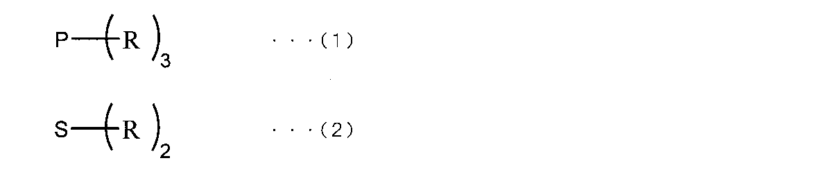
- R each independently represents an organic group, and each R may be the same as or different from each other.
- each R independently represents a vinyl group, an acryl group, a methacryl group, a maleate group, a maleate amide group, or a maleate imide group.
- the loss tangent (tan ⁇ ) defined by the ratio (G ′′ / G ′) of the loss elastic modulus (G ′′) and the storage elastic modulus (G ′) at 1 Hz at 60 ° C. is The conductive adhesive film according to any one of [1] to [5] above, which is 1.4 or more.
- the resin (M) includes a thermosetting resin (M1), 1st metal particle (Q1) which the said metal particle (Q) consists of 1 type of metal selected from the group of copper, nickel, aluminum, and tin, or the alloy containing 2 or more types selected from these groups
- thermosetting resin (M1) includes an epoxy resin having a molecular skeleton derived from a glycidyl ether of an aliphatic diol.
- thermosetting resin (M1) further includes a phenol novolac resin.
- the first metal particles (Q1) and the second metal particles (Q2) contain a metal component capable of forming an intermetallic compound with each other.
- the second metal particle (Q2) is one metal selected from the group consisting of copper, nickel, aluminum, tin, zinc, titanium, silver, gold, indium, bismuth, gallium, and palladium, or these
- the storage elastic modulus at 1 Hz measured at 1 is 20 GPa or less, and the heating weight reduction rate when heated at 250 ° C.
- a lead-free element-bearing part or a circuit electrode part of an insulating substrate a lead-free bonding layer with excellent heat resistance after bonding and sintering and mounting reliability can be formed Further, it is possible to provide a conductive adhesive film suitable for use as a conductive bonding material and a dicing die bonding film using the same.
- the conductive adhesive film according to this embodiment includes metal particles (Q), a resin (M), and at least one of a predetermined organic phosphine (A) and a predetermined sulfide-based compound (B).
- the conductive adhesive film may further contain various additives as necessary.
- metal particles means not only metal particles composed of a single metal component, but also alloy particles composed of two or more metal components, unless otherwise specified. Also means.
- the metal particles (Q) are one kind of metal selected from the group of copper (Cu), nickel (Ni), aluminum (Al), and tin (Sn), or these It is preferable to include the first metal particles (Q1) made of an alloy containing two or more selected from the group.
- Such first metal particles (Q1) are suitable as the metal particles (Q) of the conductive adhesive film in that they are excellent in conductivity and thermal conductivity, are relatively inexpensive, and hardly cause ion migration.
- the metal particles (Q) may consist of only the first metal particles (Q1), or one or more other metal particles in addition to the first metal particles (Q1). It may be a mixture containing.
- the metal particle (Q) is a mixture including the first metal particle (Q1) and the second metal particle (Q2) of a metal component system different from the first metal particle (Q1).
- the metal particles (Q1) and the second metal particles (Q2) preferably contain a metal component capable of forming an intermetallic compound. Since the first metal particles (Q1) and the second metal particles (Q2) contain a metal capable of forming an intermetallic compound, the metal particles (Q) as a whole are in an unsintered state. Then, although it is a low melting point metal or alloy, it becomes possible to form a high melting point intermetallic compound in the state after sintering. As a result, according to such metal particles, it is possible to achieve excellent heat resistance without degrading the performance after sintering even at a temperature higher than the mounting temperature, while achieving a low mounting temperature. .
- a combination of metal components capable of forming such an intermetallic compound can be selected as appropriate.
- Cu—Sn, Ni—Sn, Ag—Sn, Cu—Zn, Ni—Zn, Ni Combinations of —Ti, Sn—Ti, Al—Ti, and the like can be given.
- Each metal component corresponding to the combination that can form these intermetallic compounds is included in each of the first metal particles (Q1) and the second metal particles (Q2). It is preferable.
- a combination containing Sn having a low melting point is preferable, and a combination of Cu—Sn or Ni—Sn is particularly preferable.
- the second metal particles (Q2) have a metal component system different from that of the first metal particles (Q1), and can form an intermetallic compound with the first metal particles (Q1).
- a metal component but preferably copper (Cu), nickel (Ni), aluminum (Al), tin (Sn), zinc (Zn), titanium (Ti), silver ( Contains one metal selected from the group of Ag), gold (Au), indium (In), bismuth (Bi), gallium (Ga) and palladium (Pd), or two or more selected from these groups Made of alloy.
- the first metal particles (Q1) are Cu particles
- the second metal particles (Q2) are metal particles that can form an intermetallic compound with Cu, such as Sn particles or Alloy particles containing Sn are preferable.
- At least one of the first metal particles (Q1) and the second metal particles (Q2) is an alloy particle containing two or more kinds of metal components.
- the metal particles (Q) as a whole can be further lowered in melting point.
- alloy particles include copper (Cu), nickel (Ni), aluminum (Al), tin (Sn), zinc (Zn), titanium (Ti), silver (Ag), gold (Au),
- An alloy containing at least two selected from indium (In), bismuth (Bi), gallium (Ga) and palladium (Pd) is preferable.
- examples of such alloy particles include those obtained by adding Zn, Bi, Ag, In, Ga, Pd, or the like to Sn or the like and alloying them in advance.
- the content of the first metal particles (Q1) in 100% by mass of the metal particles (Q) is preferably 10 to 100% by mass, more preferably 30 to 80% by mass.
- the content of the second metal particles (Q2) in 100% by mass of the metal particles (Q) is preferably 0 to 90% by mass, more preferably 20 to 70% by mass.
- the metal particles (Q) may further include other metal particles (Qn) made of a single metal or an alloy as necessary. One or more kinds may be contained, and the content thereof is preferably 50% by mass or less in 100% by mass of the metal particles (Q).
- a metal particle (Q) does not contain Pb (lead), Hg (mercury), Sb (antimony), and As (arsenic) substantially from a viewpoint of environmental impact reduction.
- content of these components is less than 0.1 mass% in total in 100 mass% of metal particles (Q).
- the shape of the metal particles (Q) is not particularly limited, and spherical particles, dendritic particles, scaly shapes, spike shapes, and the like can be used as appropriate. Further, the particle diameter of the metal particles (Q) is not particularly limited, but the average particle diameter (D50) is preferably 20 ⁇ m or less. By setting the particle diameter of the metal particles (Q) within the above range, the conductive adhesive film can be formed in a relatively thin film (for example, 40 ⁇ m or less).
- the first metal particles (Q1) and the second metal particles (Q2) are used, for example, the first metal particles (Q1) have an average particle diameter (D50) of 20 ⁇ m or less,
- the two metal particles (Q2) preferably have an average particle diameter (D50) of less than 7 ⁇ m.
- the average particle diameter (D50) is a value calculated based on measurement by a laser diffraction / scattering particle size distribution measurement method.
- the measurement conditions of average particle diameter (d50) are demonstrated in the term of the Example mentioned later.
- the content of the metal particles (Q) in the conductive adhesive film according to the present embodiment is preferably 70 to 96% by mass, more preferably 80 to 94% by mass.
- the resin (M) preferably includes a thermosetting resin (M1).
- the thermosetting resin (M1) the conductive adhesive film contributes to film properties (ease of molding, ease of handling, etc.) in an unsintered state, and in a state after sintering, It plays the role of relieving stress and the like generated between the semiconductor element and the base material (lead frame or the like) by the thermal cycle.
- the thermosetting resin (M1) is a maleic imide containing a maleic imide compound containing 2 units or more of imide groups in one molecule, particularly from the viewpoint of heat resistance and film properties when the metal particles (Q) are mixed. It is preferable to include a resin (hereinafter sometimes referred to as “maleimide resin”) or an epoxy resin having a molecular skeleton derived from a glycidyl ether of an aliphatic diol, and more preferably a maleic imide resin.
- maleimide resin a resin having a molecular skeleton derived from a glycidyl ether of an aliphatic diol
- the thermosetting resin (M1) containing any of the above resins is excellent in stress relaxation properties, the heat resistant fatigue characteristics can be improved in the conductive adhesive film after sintering.
- thermosetting resin (M1) As a result, according to the conductive adhesive film containing such a thermosetting resin (M1), it is possible to overcome the drawbacks of the heat-resistant fatigue characteristics of being hard and brittle, which was a problem of conventional lead-free solders made of only metals. .
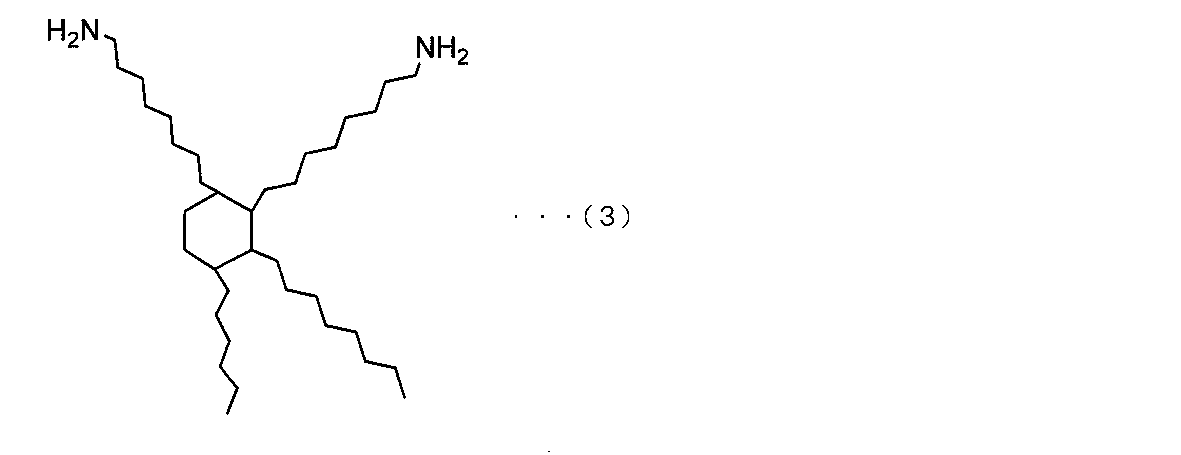
- the maleic imide resin can be obtained, for example, by condensing maleic acid or an anhydride thereof with diamine or polyamine. Further, the maleic imide resin preferably contains a skeleton derived from an aliphatic amine having 10 or more carbon atoms from the viewpoint of stress relaxation, and particularly has 30 or more carbon atoms, and is represented by the following structural formula (3). Those having a simple skeleton are more preferred.
- the maleic imide compound preferably has a number average molecular weight of 3000 or more.
- the maleic imide resin contains a skeleton derived from an acid component other than maleic acid, for example, benzenetetracarboxylic acid or its anhydride, hydroxyphthalic acid bisether or its anhydride, etc., so that the molecular weight or glass transition temperature Tg can be obtained. Etc. may be adjusted. Moreover, as a hardening
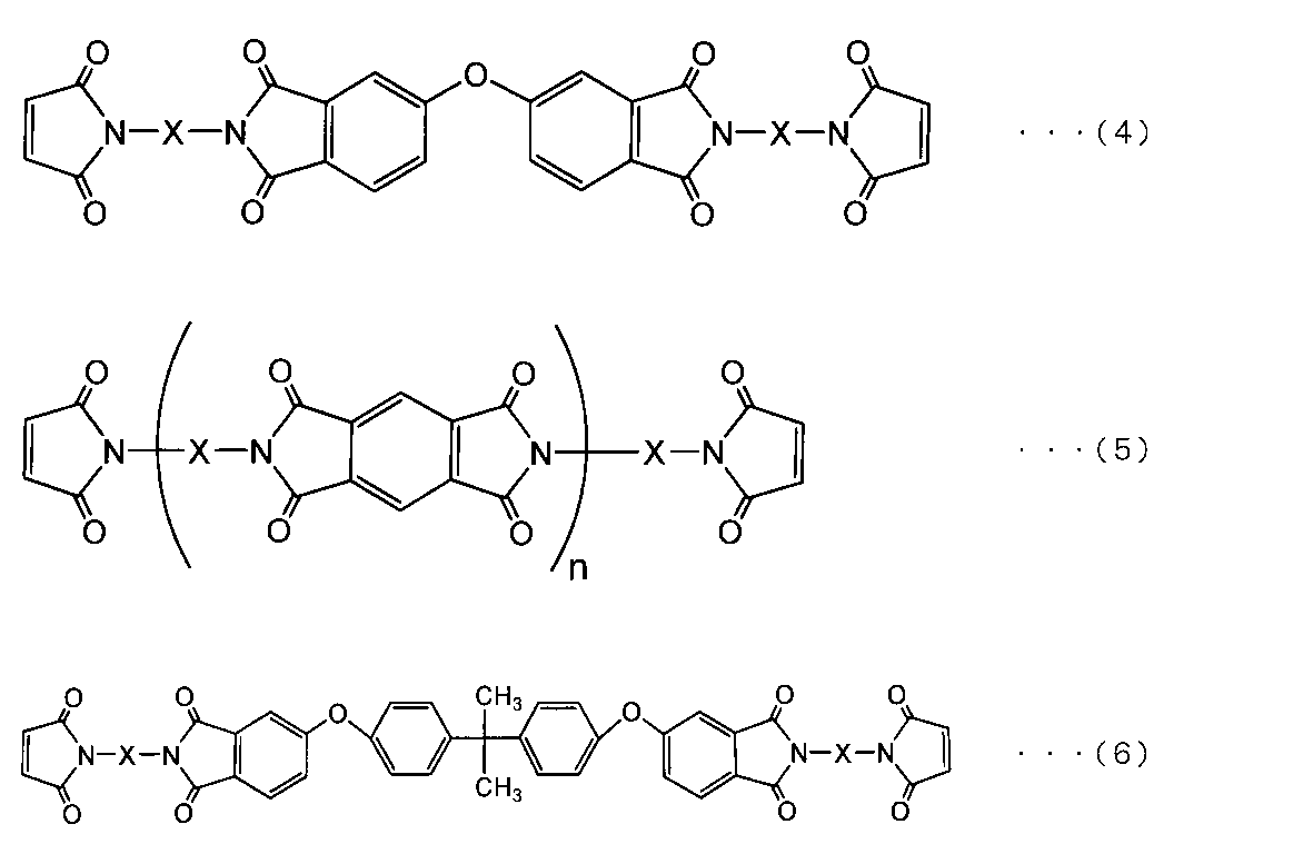
- maleic imide resin for example, bismaleimide resins represented by the following structural formulas (4) to (6) are preferably used.
- n is an integer of 1 to 10.
- the portion “X” is a skeleton of “C 36 H 72 ” represented by the following structural formula (7).
- “*” means a binding site with N.
- examples of the epoxy resin having a molecular skeleton derived from glycidyl ether of aliphatic diol include ethylene glycol-modified epoxy resin, propylene glycol-modified epoxy resin, butanediol-modified epoxy resin, and the like. These epoxy resins are preferable from the viewpoint of flexibility. Further, such an epoxy resin is used in combination with a bisphenol A type epoxy resin, a bisphenol F type epoxy resin, a phenoxy resin which is an epoxy resin having a large molecular weight, or the like from the viewpoint of achieving both adhesive strength and flexibility. preferable.
- epoxy resin curing agent acid anhydrides, phenol novolac resins, amines, imidazole compounds, dicyandiamide, and the like can be selected. Of these, phenol novolac resins and imidazole compounds are preferred.
- the thermosetting resin (M1) preferably further contains a phenol novolac resin.
- a phenol novolac resin By using the maleic imide resin or epoxy resin in combination with a phenol novolac resin, the phenol novolac resin acts as a curing agent, and the adhesiveness of the conductive adhesive film is further improved.
- the content of the resin (M) in the conductive adhesive film according to this embodiment is preferably 4 to 30% by mass, more preferably 6 to 20% by mass.
- resin (M) may consist of only one type of resin, or may be a mixture of two or more types of resins. Moreover, you may further contain resin other than the above as needed.
- Organic phosphines (A) and sulfide compounds (B) The conductive adhesive film according to this embodiment includes at least one of an organic phosphine (A) represented by the following general formula (1) and a sulfide compound (B) represented by the following general formula (2).
- R each independently represents an organic group, and R may be the same or different from each other.
- These compounds have a function as a flux that assists in removing the oxide film on the surface of the metal particle (Q) in the conductive adhesive film according to the present embodiment, and in particular, Cu, Sn, Ni, and Al. It works more effectively against such easily oxidizable metals. In addition, these compounds are extremely difficult to absorb moisture and are excellent in moisture absorption resistance as compared with fluxes such as carboxylic acids and alcohols that have been generally used conventionally.
- each R is independently selected from an alkyl group, an aryl group, an organic group having a functional group, an organic group having a hetero atom, and an organic group having an unsaturated bond. And at least one of R is preferably an aryl group.
- the alkyl group may be linear, branched or cyclic, and may have a substituent.
- the alkyl group is preferably linear or branched.
- the alkyl group preferably has 3 or more carbon atoms, more preferably 4 to 18 carbon atoms, and still more preferably 6 to 15 carbon atoms.
- Specific examples of such alkyl groups include propyl, butyl, pentyl, hexyl, heptyl, octyl, nonyl, decyl, stearyl and isostearyl groups.
- the aryl group may have a substituent and preferably has 6 to 10 carbon atoms.
- Examples of such an aryl group include a phenyl group, a tolyl group, a xylyl group, a cumenyl group, and a 1-naphthyl group.
- the organic group having a functional group preferably has 1 to 10 carbon atoms, more preferably 1 to 6 carbon atoms, and still more preferably 1 to 3 carbon atoms.
- examples of the functional group of the organic group include a chloro group, a bromo group, and a fluoro group.
- Specific examples of the organic group having such a functional group include a chloroethyl group, a fluoroethyl group, a chloropropyl group, a dichloropropyl group, a fluoropropyl group, a difluoropropyl group, a chlorophenyl group, and a fluorophenyl group. Can be mentioned.
- the organic group having a hetero atom preferably has 3 or more carbon atoms, more preferably 4 to 18 carbon atoms, and still more preferably 6 to 15 carbon atoms. Moreover, a nitrogen atom, an oxygen atom, a sulfur atom etc. are mentioned as a hetero atom which the said organic group has. Specific examples of the organic group having a hetero atom include a dimethylamino group, a diethylamino group, a diphenylamino group, a methyl sulfoxide group, an ethyl sulfoxide group, and a phenyl sulfoxide group.
- the organic group having an unsaturated bond preferably has 3 or more carbon atoms, more preferably 4 to 18 carbon atoms, and still more preferably 6 to 15 carbon atoms.
- Specific examples of the organic group having an unsaturated bond include a propenyl group, a propynyl group, a butenyl group, a butynyl group, an oleyl group, a phenyl group, a vinylphenyl group, and an alkylphenyl group. Among these, it is more preferable to have a vinylphenyl group.
- each R is independently a vinyl group, an acrylic group, a methacryl group, a maleate group, a maleate amide group, a maleate imide group, It preferably has any one or more selected from primary amino groups, secondary amino groups, thiol groups, hydrosilyl groups, hydroboron groups, phenolic hydroxyl groups and epoxy groups. Among these, it is more preferable to have a vinyl group, an acrylic group, a methacryl group, or a secondary amino group.
- the organic phosphine (A) preferably contains p-styryldiphenylphosphine.
- Such a compound is suitable in that it has a low reactivity because it has a highly reactive vinyl group.
- the sulfide compound (B) is at least one of bis (hydroxyphenyl) sulfide, bis (acryloylthiophenyl) sulfide, 2-methylthiophenothiazine, bis (2-methacryloylthioethyl) sulfide and bis (methacryloylthiophenyl) sulfide. It preferably contains a species, and more preferably contains at least one of bis (acryloylthiophenyl) sulfide and bis (methacryloylthiophenyl) sulfide. These compounds are suitable because they have a highly reactive phenolic hydroxyl group, acrylic group, and methacryl group, and are low in bleed out, and among them, compounds having an acrylic group or a methacryl group are most preferred.
- the organic phosphines (A) and the sulfide compound (B) can be used alone or in combination.
- the conductive adhesive film according to the present embodiment contains both the organic phosphines (A) and the sulfide-based compound (B), the adhesive strength of the conductive adhesive film can be improved.
- Such organic phosphines (A) and sulfide compounds (B) can form a copolymer with the maleimide resin when the thermosetting resin (M1) includes a maleimide resin. Also acts as a curable resin component.
- the organic phosphines (A) and the sulfide-based compound (B) are difficult to absorb moisture, have a sufficiently large molecular weight, and are polymerizable, and therefore can effectively prevent bleed out when used as a flux component.
- the number average molecular weights of the organic phosphines (A) and the sulfide-based compound (B) are preferably 260 or more from the viewpoint of suppressing bleeding out during sintering. Further, the number average molecular weight of the organic phosphines (A) and the sulfide-based compound (B) is set to 260 or more, and the bleed out can be further reduced by reacting with the maleimide resin and curing as described above. As a result, surface contamination of the substrate (such as a lead frame) due to bleed-out can be prevented, and package reliability can be improved.
- the content of the organic phosphines (A) in the conductive adhesive film according to this embodiment is preferably 0.5 to 10.0% by mass, more preferably 1.0 to 5.0% by mass. By setting it within the above range, the metal oxide film removing ability is sufficiently exhibited.
- the content of the sulfide-based compound (B) in the conductive adhesive film according to this embodiment is preferably 0.5 to 8.0% by mass, and more preferably 1.0 to 4.0% by mass. By setting it within the above range, the metal oxide film removing ability is sufficiently exhibited.
- the total content is preferably 0.5 to 10.0 mass. %, More preferably 1.0 to 5.0% by mass.
- organic phosphines (A) and sulfide compounds (B) may be used alone or in combination of two or more.
- the conductive adhesive film according to the present embodiment may contain various additives in addition to the above components as long as they do not depart from the object of the present invention.
- Such an additive can be appropriately selected as necessary, and examples thereof include a dispersant, a radical polymerization initiator, a leveling agent, and a plasticizer.
- the conductive adhesive film according to this embodiment has a film shape. Therefore, for example, when connecting the power semiconductor element to the substrate, handling becomes easier than conventional solder or conductive paste.
- the conductive adhesive film according to the present embodiment is attached to the back surface of the wafer on which the power semiconductor is formed, and is divided into wafers when the wafer is divided into chips (dicing process). It becomes possible to do. Therefore, since the conductive adhesive film can be formed on the entire back surface of the element (wafer) without excess or deficiency, it is possible to achieve good mounting without causing problems such as conventional solder wettability and protrusion.
- the conductive adhesive film can be formed in a predetermined thickness in advance, the height of the element after die bonding can be controlled accurately and easily compared to conventional solder or conductive paste.
- the method for producing the conductive adhesive film of the present embodiment is not particularly limited, and can be performed by a known method.
- an appropriate amount of each of the above components is weighed and mixed by a known method, and the resulting mixture is formed into a film by a known method.
- Examples of such a mixing method include stirring and mixing using a rotary blade, mixing using a homogenizer, mixing using a planetary mixer, mixing using a kneader, and the like.
- a molding method for example, a method in which a varnish in which the above mixture is dissolved and dispersed in a solvent is applied on a substrate and then dried, a melt coating in which a conductive adhesive film is melted at a high temperature and then applied to the substrate.
- a method of pressing a conductive adhesive film together with a substrate at a high pressure an extrusion method in which a conductive adhesive film is melted and then extruded using an extruder, and then stretched, and the varnish is screen mesh (screen printing) or a metal plate
- the printing method include filling and transferring (gravure printing).
- the thickness of the conductive adhesive film is preferably 5 to 100 ⁇ m, more preferably 20 to 50 ⁇ m. By setting the thickness of the conductive adhesive film within the above range, it is possible to obtain a sufficient adhesive force while suppressing electrical resistance and thermal resistance.
- the conductive adhesive film according to this embodiment has a storage elastic modulus at 1 Hz measured in a state after sintering of 20 GPa or less.
- the storage elastic modulus is preferably 1000 to 20000 MPa, more preferably 5000 to 20000 MPa.
- the measuring method of a storage elastic modulus is demonstrated in the item of the Example mentioned later.
- the conductive adhesive film according to this embodiment has a heating weight reduction rate of less than 1% when heated at 250 ° C. for 2 hours in a nitrogen atmosphere.
- the heating weight reduction rate within the above range, when the conductive adhesive film is sintered, the resin is mainly not thermally decomposed, so that the reliability can be ensured by the excellent low bleed-out property.
- the measuring method of a heating weight decreasing rate is demonstrated in the item of the Example mentioned later.
- the endothermic peak in the temperature range of 100 to 250 ° C. is in a state before sintering (unburned) when analyzed by DSC (differential scanning calorimetry). It is preferable that at least one is observed in the (bonded state) and disappears in the state after sintering (sintered state).
- At least one endothermic peak observed in the above temperature range in an unsintered state means a melting point of a metal or alloy containing at least one metal component. That is, when an unsintered conductive adhesive film is heated (sintered) in the above temperature range, a specific metal component melts and spreads on the surface of the adherend, which is advantageous for mounting at a low temperature. Shows that it works.
- the sintered state no endothermic peak is observed in the above temperature range, but this is because there is no melting point of a metal component (or alloy) of a metal or alloy containing at least one metal component in the above temperature range. Means. That is, it is shown that the metal once melted forms an intermetallic compound having a high melting point after sintering by a diffusion reaction between the metals, and as a result, has excellent heat resistance.
- Such conductive adhesive films can be sintered (mounted) at low temperatures, but after sintering (after mounting), they exhibit excellent heat resistance, and can be wire-bonded with high melting point lead-free solder. Even if the reflow process is performed, no problem occurs.
- the heat resistant temperature of the conductive adhesive film is preferably 250 ° C. or higher, more preferably 300 ° C. or higher.
- a suitable mounting temperature when mounting a semiconductor chip or the like using the conductive adhesive film is preferably 100 to 250 ° C., and more preferably 100 to 200 ° C.
- the measurement conditions are a measurement temperature range of room temperature to 350 ° C., a temperature rising rate of 5 ° C./min, a nitrogen flow rate of 20 mL / min, and an aluminum sample pan.
- the conductive adhesive film according to the present embodiment is defined by the ratio (G ′′ / G ′) of the loss elastic modulus (G ′′) and storage elastic modulus (G ′) at 1 Hz at 60 ° C. in the B stage state.
- the loss tangent (tan ⁇ ) is preferably 1.4 or more. The larger tan ⁇ under the above conditions, the better the conductive adhesive film is.
- the method for measuring and calculating the loss elastic modulus (G ′′), storage elastic modulus (G ′), and tan ⁇ will be described in the Examples section described later.
- the B stage state is the heat in DSC measurement. It means a state in which 80% or more of the calorific value before curing derived from the curable resin component is retained.
- the conductive adhesive film according to the present embodiment can be bonded to a dicing tape to form a dicing die bonding film, so that the conductive adhesive film and the dicing tape can be bonded to the wafer at one time, and the process is omitted. it can.
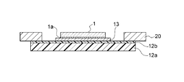
- FIG. 1 is a sectional view showing a dicing die bonding film 10 according to the present invention.
- the dicing die bonding film 10 is mainly composed of a dicing tape 12 and a conductive adhesive film 13.
- the dicing die bonding film 10 is an example of a semiconductor processing tape, and may be cut into a predetermined shape (pre-cut) in advance according to a use process or an apparatus, or cut for each semiconductor wafer. Alternatively, it may have a long roll shape.
- the dicing tape 12 includes a support base 12a and an adhesive layer 12b formed thereon.
- the release-treated PET film 11 covers the dicing tape 12 and protects the pressure-sensitive adhesive layer 12 b and the conductive adhesive film 13.
- the support substrate 12a is preferably radiolucent, and specifically, plastic or rubber is usually used, and is not particularly limited as long as it transmits radiation.
- the base resin composition of the pressure-sensitive adhesive layer 12b is not particularly limited, and a normal radiation curable pressure-sensitive adhesive is used.
- An acrylic pressure-sensitive adhesive having a functional group capable of reacting with an isocyanate group such as a hydroxyl group is preferred.
- the acrylic pressure-sensitive adhesive preferably has an iodine value of 30 or less and has a radiation-curable carbon-carbon double bond structure.
- Q metal particle
- resin resin
- prescribed organic phosphine A
- prescribed sulfide type compound B.
- a conductive adhesive film containing at least one of them is very preferable in terms of excellent heat resistance and mounting reliability when the semiconductor power element is bonded to the metal lead frame and having a small environmental load.
- the dicing / die bonding film 10 of the present embodiment can be suitably used.
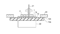
- the release-treated PET film 11 is removed from the dicing die bonding film 10, and as shown in FIG. 2, the conductive adhesive film 13 is attached to the semiconductor wafer 1 and the side portion of the dicing tape 12 is fixed by the ring frame 20.
- the ring frame 20 is an example of a dicing frame.
- the conductive adhesive film 13 is laminated on a portion of the dicing tape 12 where the semiconductor wafer 1 is bonded. There is no conductive adhesive film 13 in the portion of the dicing tape 12 that contacts the ring frame 20.
- the semiconductor wafer 1 is diced into a predetermined size by using the dicing blade 21 while the lower surface of the dicing tape 12 is sucked and fixed by the suction stage 22 to manufacture a plurality of semiconductor chips 2.
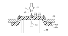
- the tape push-up ring 30 is raised, the central portion of the dicing tape 12 is bent upward, and radiation such as ultraviolet rays is radiated.
- the adhesive strength of the adhesive layer 12b constituting the dicing tape 12 is weakened.
- the push-up pin 31 is raised at a position corresponding to each semiconductor chip, and the semiconductor chip 2 is picked up by the suction collet 32.
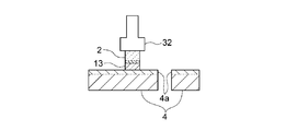
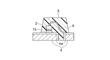
- the picked-up semiconductor chip 2 is bonded to a supporting member such as the lead frame 4 or another semiconductor chip 2 (die bonding process), and the conductive adhesive film is sintered.
- a semiconductor device is obtained through steps such as attachment of an Al wire and resin molding.
- the average particle diameter (D50) of the metal particles was measured with a laser diffractometer (SALD-3100, manufactured by Shimadzu Corporation).
- Thermosetting resin (M1) Maleimide resin A mixture of BMI-3000 and perbutyl (registered trademark) O as a polymerization initiator mixed at a mass ratio of 100: 5.
- BMI-3000 Bismaleimide resin represented by DESIGNER MOLECULES INC, number average molecular weight 3000, represented by the following structural formula (8).
- n is an integer of 1 to 10. Note that the skeleton derived from the aliphatic amine has 36 carbon atoms.
- -Phenol novolac resin H-4 manufactured by Meiwa Kasei Co., Ltd.
- Epoxy resin 1 A mixture of YD-128, YD-013, YP-50 and 2PHZ mixed at a mass ratio of 15: 5: 10: 1.
- YD-128 Nippon Steel & Sumikin Chemical Co., Ltd., bisphenol A type liquid epoxy resin.
- YD-013 A bisphenol A type solid epoxy resin manufactured by Nippon Steel & Sumikin Chemical Co., Ltd.
- YP-50 manufactured by Nippon Steel & Sumikin Chemical Co., Ltd., phenoxy resin.
- 2PHZ 2-phenyl-4,5-dihydroxymethylimidazole manufactured by Shikoku Kasei Kogyo Co., Ltd.
- EP4000L Propylene glycol-modified epoxy resin manufactured by ADEKA Corporation.
- -Phenol novolac resin H-4 manufactured by Meiwa Kasei Co., Ltd.
- Example 1 a mixture of materials shown in Table 1 among the above materials was prepared so that the ratio of metal particles (Q) was 91.5% by mass, resin (M) was 5.5% by mass, and flux was 3% by mass. Then, toluene is added as a solvent to make a slurry, and after stirring with a planetary mixer, it is thinly coated on a release-treated PET film, dried at 120 ° C. for 2 minutes, and conductive adhesive with a thickness of 40 ⁇ m. A film was obtained.
- the metal particle (Q) used here consists only of spherical copper powder as a 1st metal particle (Q1).
- Example 2 In Example 2, in 100% by mass of the metal particles (Q), the ratio of the spherical copper powder as the first metal particles (Q1) is 60% by mass and the spherical tin powder is 40% by mass as the second metal particles (Q2). Thus, a conductive adhesive film was obtained in the same manner as in Example 1 except that the metal particles (Q) were adjusted.
- Example 3 Maleimide resin was used as the resin (M), and organic phosphines were used as the flux.
- spherical copper powder was 60% by mass as the first metal particles (Q1)
- a conductive adhesive film was obtained in the same manner as in Example 1 except that the metal particles (Q) were adjusted so that the spherical tin powder had a ratio of 40% by mass as the second metal particles (Q2). .
- Example 4 In Example 4, a conductive adhesive film was obtained in the same manner as in Example 3 except that sulfide compound 2 was used as the flux.
- Example 5 a conductive adhesive film was prepared in the same manner as in Example 4 except that a flux prepared so that the ratio of organic phosphines to 25% by mass and sulfide compound 2 to 75% by mass was used. Got.
- Example 6 In Example 6, the same method as in Example 5 was used except that the resin (M) prepared so that the ratio of maleimide resin 3 to 95% by mass and phenol novolac resin to 5% by mass was used. Adhesive film was obtained.
- Comparative Examples 1 and 2 In Comparative Examples 1 and 2, a mixture of materials shown in Table 1 among the above materials was prepared so that the ratio of metal particles (Q) was 85% by mass, resin (M) was 8% by mass, and flux was 7% by mass. Except for the above, a conductive adhesive film was obtained in the same manner as in Example 1.
- Comparative Example 3 a conductive adhesive film was produced in the same manner as in Example 1 except that the materials shown in Table 1 among the above materials were used. However, the coating film after drying was extremely brittle and hard solid, had no adhesiveness, and could not be used as a conductive adhesive film.
- the obtained measurement sample was subjected to MSL-Lv1 and 2 in a post-moisture reflow test (lead-free solder compliant) defined in JEDEC J-STD-020D1 under the following conditions. Thereafter, it was observed whether peeling occurred inside using an ultrasonic imaging apparatus (FineSAT, manufactured by Hitachi Power Solution Co., Ltd.). In this example, at least MSL-Lv2 and no PKG peeling were considered acceptable.
- MSL-Lv1 is 168 hours at 85 ° C. and 85% RH.
- MSL-Lv2 is 168 hours at 85 ° C. and 60% RH.
- Reflow grade temperature MSL-Lv1 and 2 are both 260 ° C.
- the scratch tool of the bond tester was made to collide with the side surface of the semiconductor chip of the measurement sample at 100 ⁇ m / s.
- the stress at the time when the chip / lead frame junction was broken was measured as the shear adhesive strength at 260 ° C.
- the shear adhesive strength before TCT was set to an acceptable level of 3 MPa or more.
- volume resistivity (conductivity)
- the conductive adhesive films according to the above Examples and Comparative Examples were placed on a Teflon (registered trademark) sheet and sintered at 230 ° C. for 3 hours to obtain a measurement sample.
- the resistance value of this measurement sample was measured by the four-probe method according to JIS-K7194-1994, and the volume resistivity was calculated.
- Lorester GX manufactured by Mitsubishi Chemical Analytech Co., Ltd. was used for measurement of the resistance value.
- the volume resistivity means that the reciprocal thereof is the conductivity, and the smaller the volume resistivity, the better the conductivity.
- the volume resistivity was set to 1000 ⁇ ⁇ cm or less as an acceptable line.
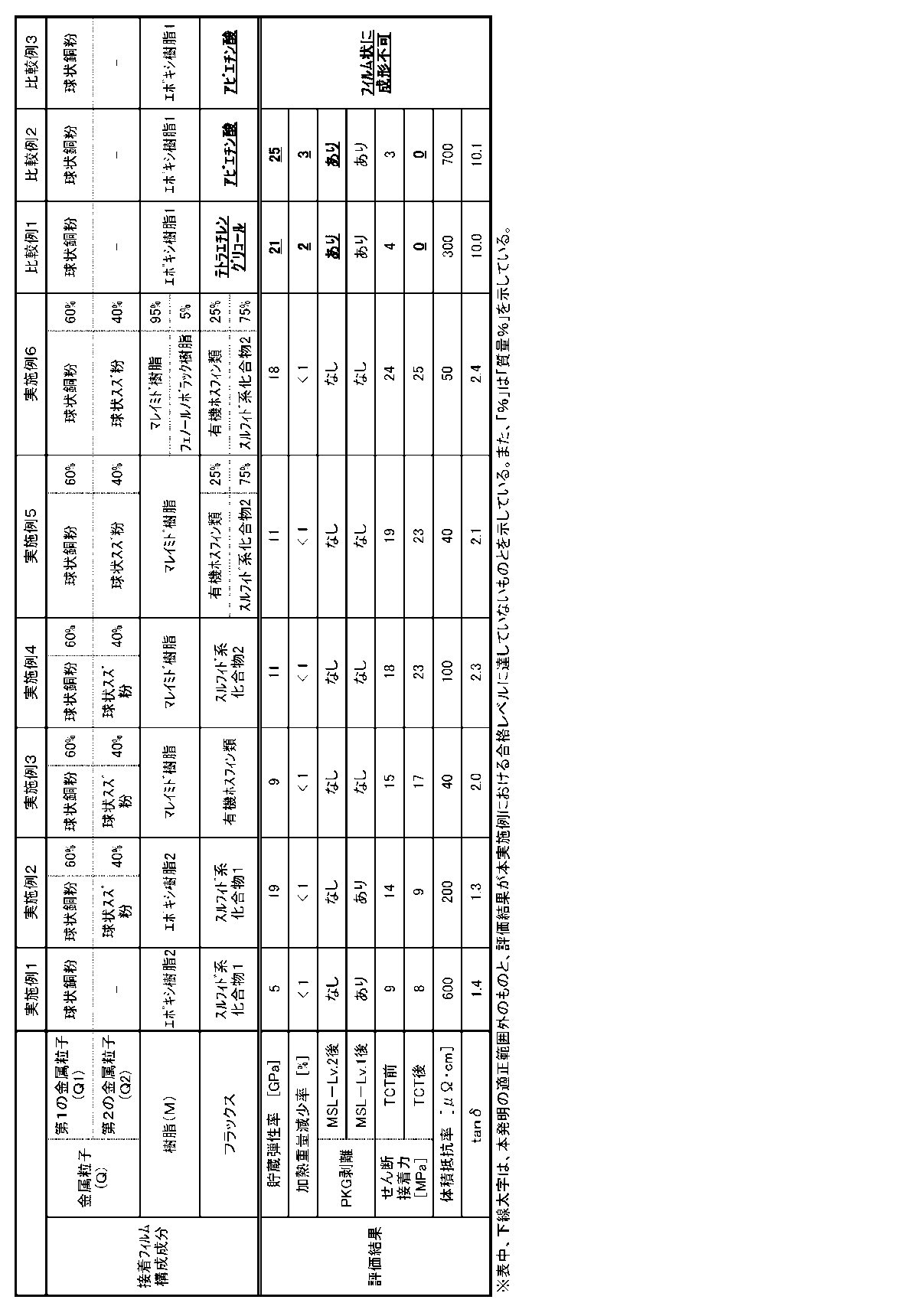
- the conductive adhesive films according to Examples 1 to 6 have at least metal particles (Q), a resin (M), a predetermined organic phosphine (A), and a predetermined sulfide-based compound (B).
- Q metal particles
- M resin
- A predetermined organic phosphine
- B predetermined sulfide-based compound
- the conductive adhesive films according to Comparative Examples 1 and 2 do not contain any of the predetermined organic phosphines (A) and the predetermined sulfide compound (B) specified in the present invention.
- the heat resistance after bonding and sintering and the mounting reliability were both inferior.
- PKG peeling occurred even in MSL-Lv2, and it was confirmed that the moisture absorption resistance was particularly poor.
- the shear adhesive force was remarkably reduced and it was confirmed that the thermal shock resistance was inferior.
- Comparative Example 1 has a lower volume resistivity than Example 1, and at first glance, it appears to be excellent in conductivity. However, in Comparative Example 1, peeling has already occurred in the moisture absorption test of MSL-Lv2, and the resistance value is infinite in this state, so it cannot be said that the conductivity is excellent from a practical viewpoint. . Moreover, the comparative example 1 is also inferior in the adhesive force after TCT. That is, from the viewpoint of practicality, as in Example 1, even if the conductivity itself is somewhat low, it has excellent heat resistance and moisture absorption resistance, and can achieve stable conduction, and has high mounting reliability. It can be said that a film is preferable.
- Comparative Example 3 is a predetermined organic material specified in the present invention. Since neither the phosphine (A) nor the predetermined sulfide-based compound (B) was contained, the mixture was not collected and could not be formed into a sheet. That is, when the content of the metal particles (Q) is increased by containing at least one of the predetermined organic phosphines (A) and the predetermined sulfide-based compound (B) specified in the present invention. As a result, it was confirmed that favorable sheet formation was possible (Examples 1 to 6).
Landscapes
- Chemical & Material Sciences (AREA)
- Organic Chemistry (AREA)
- Physics & Mathematics (AREA)
- Dispersion Chemistry (AREA)
- Spectroscopy & Molecular Physics (AREA)
- Chemical Kinetics & Catalysis (AREA)
- Inorganic Chemistry (AREA)
- Die Bonding (AREA)
- Adhesives Or Adhesive Processes (AREA)
- Adhesive Tapes (AREA)
- Health & Medical Sciences (AREA)
- Medicinal Chemistry (AREA)
- Polymers & Plastics (AREA)
- Dicing (AREA)
- Conductive Materials (AREA)
Abstract
Description
[1] 金属粒子(Q)と、樹脂(M)と、下記一般式(1)で示される有機ホスフィン類(A)および下記一般式(2)で示されるスルフィド系化合物(B)の少なくとも一方とを含み、
焼結後の状態で測定した1Hzにおける貯蔵弾性率が、20GPa以下であり、
窒素雰囲気下、250℃で2時間加熱したときの加熱重量減少率が、1%未満である、導電性接着フィルム。
[2] 前記一般式(1)および(2)のそれぞれにおいて、Rの少なくとも1つは、アリール基である、上記[1]に記載の導電性接着フィルム。
[3] 前記一般式(1)および(2)において、Rは、それぞれ独立して、その一部にビニル基、アクリル基、メタクリル基、マレイン酸エステル基、マレイン酸アミド基、マレイン酸イミド基、1級アミノ基、2級アミノ基、チオール基、ヒドロシリル基、ヒドロホウ素基、フェノール性水酸基およびエポキシ基から選択されるいずれか1種以上を有する、上記[1]または[2]に記載の導電性接着フィルム。
[4] 前記有機ホスフィン類(A)は、p-スチリルジフェニルホスフィン含む、上記[1]~[3]のいずれか1項に記載の導電性接着フィルム。
[5] 前記スルフィド系化合物(B)は、ビス(アクリロイルチオフェニル)スルフィドおよびビス(メタクリロイルチオフェニル)スルフィドの少なくとも一方を含む、上記[1]~[4]のいずれか1項に記載の導電性接着フィルム。
[6] Bステージ状態において、60℃で1Hzにおける損失弾性率(G’’)と貯蔵弾性率(G’)との比(G’’/G’)で定義される損失正接(tanδ)が、1.4以上である、上記[1]~[5]のいずれか1項に記載の導電性接着フィルム。
[7] 前記樹脂(M)は、熱硬化性樹脂(M1)を含み、
前記金属粒子(Q)が、銅、ニッケル、アルミニウムおよびスズの群から選択される1種の金属またはこれらの群から選択される2種以上を含有する合金からなる第1の金属粒子(Q1)を含む、上記[1]~[6]のいずれか1項に記載の導電性接着フィルム。
[8] 前記熱硬化性樹脂(M1)は、イミド基を1分子中に2単位以上有するマレイン酸イミド化合物を含む、上記[7]に記載の導電性接着フィルム。
[9] 前記熱硬化性樹脂(M1)は、脂肪族ジオールのグリシジルエーテルに由来する分子骨格を有するエポキシ樹脂を含む、上記[7]に記載の導電性接着フィルム。
[10] 前記熱硬化性樹脂(M1)が、フェノールノボラック樹脂をさらに含む、上記[8]または[9]に記載の導電性接着フィルム。
[11] 前記金属粒子(Q)が、前記第1の金属粒子(Q1)と、該第1の金属粒子(Q1)とは異なる金属成分系の第2の金属粒子(Q2)とを含む混合物であり、
前記第1の金属粒子(Q1)および前記第2の金属粒子(Q2)が、互いに、金属間化合物を形成し得る金属成分を含む、上記[7]~[10]のいずれか1項に記載の導電性接着フィルム。
[12] 前記第2の金属粒子(Q2)が、銅、ニッケル、アルミニウム、スズ、亜鉛、チタン、銀、金、インジウム、ビスマス、ガリウムおよびパラジウムの群から選択される1種の金属またはこれらの群から選択される2種以上を含有する合金からなる、上記[11]に記載の導電性接着フィルム。
[13] 上記[1]~[12]のいずれか1項に記載の導電性接着フィルムと、ダイシングテープとを貼り合せてなる、ダイシング・ダイボンディングフィルム。
本実施形態に係る導電性接着フィルムは、金属粒子(Q)と、樹脂(M)と、所定の有機ホスフィン類(A)および所定のスルフィド系化合物(B)の少なくもとも一方とを含む。また、導電性接着フィルムは、必要に応じて、さらに各種添加剤を含有してもよい。
なお、ここでいう「金属粒子」とは、特に区別して記載しない限りは、単一の金属成分からなる金属粒子のことを意味するだけではなく、2種以上の金属成分からなる合金粒子のことも意味する。
本実施形態に係る導電性接着フィルムにおいて、金属粒子(Q)は、銅(Cu)、ニッケル(Ni)、アルミニウム(Al)およびスズ(Sn)の群から選択される1種の金属またはこれらの群から選択される2種以上を含有する合金からなる第1の金属粒子(Q1)を含むことが好ましい。このような第1の金属粒子(Q1)は、導電性および熱伝導性に優れ、比較的安価で、イオンマイグレーションが起こりにくい点で、導電性接着フィルムの金属粒子(Q)として好適である。なお、金属粒子(Q)は、第1の金属粒子(Q1)のみからなるものであってもよいし、あるいは、第1の金属粒子(Q1)に加えて、他の金属粒子を1種以上含む混合物であってもよい。
本実施形態に係る導電性接着フィルムにおいて、樹脂(M)は、熱硬化性樹脂(M1)を含むことが好ましい。導電性接着フィルムが、熱硬化性樹脂(M1)を含むことにより、未焼結の状態では、フィルム性(成形のしやすさ、取り扱いやすさ等)に寄与し、焼結後の状態では、熱サイクルによって、半導体素子と基材(リードフレーム等)との間に生じる応力等を緩和する役割を果たす。

本実施形態に係る導電性接着フィルムは、下記一般式(1)で示される有機ホスフィン類(A)および下記一般式(2)で示されるスルフィド系化合物(B)の少なくもとも一方を含む。
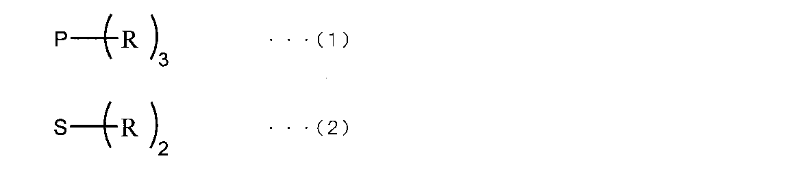
本実施形態に係る導電性接着フィルムは、上記成分の他に、本発明の目的を外れない範囲で、各種添加剤を含んでいてもよい。このような添加剤としては、必要に応じて適宜選択できるが、例えば、分散剤、ラジカル重合開始剤、レベリング剤、可塑剤等が挙げられる。
図1は、本発明にかかるダイシング・ダイボンディングフィルム10を示す断面図である。ダイシング・ダイボンディングフィルム10は、主にダイシングテープ12、導電性接着フィルム13から構成されている。ダイシング・ダイボンディングフィルム10は、半導体加工用テープの一例であり、使用工程や装置にあわせて予め所定形状に切断(プリカット)されていてもよいし、半導体ウェハ1枚分ごとに切断されていてもよいし、長尺のロール状を呈していてもよい。
剥離処理PETフィルム11は、ダイシングテープ12を覆っており、粘着剤層12bや導電性接着フィルム13を保護している。
半導体装置の製造にあたり、本実施形態のダイシング・ダイボンディングフィルム10を好適に使用することができる。
以下に、使用した原料の略称を示す。
[金属粒子(Q)]
<第1の金属粒子(Q1)>
・球状銅粉:三井金属鉱業株式会社製 MA-C05K、平均粒子径(D50)は5μmである。
<第2の金属粒子(Q2)>
・球状スズ粉:三井金属鉱業株式会社製 ST-3、平均粒子径(D50)は7μmである。
・マレイミド樹脂
BMI-3000および重合開始剤としてパーブチル(登録商標)Oを、質量比100:5で混合した混合物。
BMI-3000:DESIGNER MOLECULES INC製、数平均分子量3000、下記構造式(8)で表されるビスマレイミド樹脂。下記式(8)において、nは1~10の整数である。なお、脂肪族アミンに由来する骨格は、炭素数36である。

Hー4:明和化成株式会社製。
・エポキシ樹脂1
YD-128、YD-013、YP-50および2PHZを、質量比15:5:10:1で混合した混合物。
YD-128:新日鉄住金化学株式会社製、ビスフェノールA型液状エポキシ樹脂。
YD-013:新日鉄住金化学株式会社製、ビスフェノールA型固形エポキシ樹脂。(以下において同じ。)
YP-50:新日鉄住金化学株式会社製、フェノキシ樹脂。(以下において同じ。)
2PHZ:四国化成工業株式会社製、2-フェニル-4,5-ジヒドロキシメチルイミダゾール。(以下において同じ。)
・エポキシ樹脂2
EP4000L、YD-013、YP-50および2PHZを、質量比20:5:5:1で混合した混合物。
EP4000L:株式会社ADEKA製、プロピレングリコール変性型エポキシ樹脂。
・フェノールノボラック樹脂
Hー4:明和化成株式会社製。
・有機ホスフィン類
DPPST(登録商標):北興化学工業株式会社製、ジフェニルホスフィノスチレン。
・スルフィド系化合物1
東京化成工業株式会社製、ビス(4-ヒドロキシフェニル)スルフィド
・スルフィド系化合物2
住友精化株式会社製、ビス(4-メタクリロイルチオフェニル)スルフィド
・アビエチン酸:東京化成工業株式会社製
・乾燥後の粘着剤組成物の厚さが5μmとなるように、支持基材上に粘着剤組成物を塗工し、120℃で3分間乾燥させて得た。
粘着剤組成物:n-オクチルアクリレート(大阪有機化学工業株式会社製)、2-ヒドロキシエチルアクリレート(大阪有機化学工業株式会社製)、メタクリル酸(東京化成工業株式会社製)および重合開始剤としてベンゾイルペルオキシド(東京化成工業株式会社製)を、質量比200:10:5:2で混合した混合物を、適量のトルエン中に分散し、反応温度および反応時間を調整し、官能基を持つアクリル樹脂の溶液を得た。次に、このアクリル樹脂溶液100質量部に対し、ポリイソシアネートとしてコロネートL(東ソー株式会社製)を2質量部追加し、さらに追加溶媒として適量のトルエンを加えて攪拌し、粘着剤組成物を得た。
支持基材:低密度ポリエチレンよりなる樹脂ビーズ(日本ポリエチレン株式会社製 ノバテックLL)を140℃で溶融し、押し出し機を用いて、厚さ100μmの長尺フィルム状に成形して得た。
(実施例1)
実施例1では、上記材料のうち表1に示す材料を、金属粒子(Q)91.5質量%、樹脂(M)5.5質量%およびフラックス3質量%の比率となるように混合物を調製し、これに溶剤としてトルエンを加えてスラリー化し、プラネタリーミキサーにて撹拌後、離型処理されたPETフィルム上に薄く塗布して、120℃で2分間乾燥し、厚さ40μmの導電性接着フィルムを得た。なお、ここで用いた金属粒子(Q)は、第1金属粒子(Q1)としての球状銅粉のみからなる。
実施例2では、金属粒子(Q)100質量%中に、第1金属粒子(Q1)として球状銅粉が60質量%、第2金属粒子(Q2)として球状スズ粉が40質量%の比率となるように、金属粒子(Q)を調整した以外は、実施例1と同様の方法にて、導電性接着フィルムを得た。
実施例3では、樹脂(M)としてマレイミド樹脂を、フラックスとして有機ホスフィン類をそれぞれ用い、金属粒子(Q)100質量%中に、第1金属粒子(Q1)として球状銅粉が60質量%、第2金属粒子(Q2)として球状スズ粉が40質量%の比率となるように、金属粒子(Q)を調整した以外は、実施例1と同様の方法にて、導電性接着フィルムを得た。
実施例4では、フラックスとしてスルフィド系化合物2を用いた以外は、実施例3と同様の方法にて、導電性接着フィルムを得た。
実施例5では、有機ホスフィン類が25質量%およびスルフィド系化合物2が75質量%の比率となるよう調製されたフラックスを用いた以外は、実施例4と同様の方法にて、導電性接着フィルムを得た。
実施例6では、マレイミド樹脂3が95質量%およびフェノールノボラック樹脂が5質量%の比率となるように調製された樹脂(M)を用いた以外は、実施例5と同様の方法にて、導電性接着フィルムを得た。
比較例1および2では、上記材料のうち表1に示す材料を、金属粒子(Q)85質量%、樹脂(M)8質量%、およびフラックス7質量%の比率となるように混合物を調製した以外は、実施例1と同様の方法にて、導電性接着フィルムを得た。
比較例3では、上記材料のうち表1に示す材料を用いた以外は、実施例1と同様の方法にて、導電性接着フィルムを作製した。しかし、乾燥後の塗膜は、極めて脆く、硬い固体状のもので、粘接着性もなく、導電性接着フィルムとして用いることはできなかった。
上記のようにして得られた、上記実施例および比較例に係る導電性接着フィルムを、ダイシングテープと貼り合わせて、ダイシング・ダイボンディングフィルム(導電性接着フィルム/粘着剤組成物/支持基材)を得た。
上記のようにして得られた、上記実施例および比較例に係る、導電性接着フィルムおよびダイシング・ダイボンディングフィルムを用いて、下記に示す特性評価を行った。各特性の評価条件は下記の通りである。結果を表1に示す。
上記本実施例および比較例に係る導電性接着フィルムをテフロン(登録商標)シート上で、窒素雰囲気下、250℃で、2時間加熱して焼結させた後、5mm×30mmの短冊状に切断して測定用サンプルを得た。次に、この測定用サンプルについて、動的粘弾性測定装置DMA(株式会社ユービーエム製E4000)を用いて、周波数1Hz、ひずみ量0.3%のせん断条件で、室温における貯蔵弾性率を測定した。
上記本実施例および比較例に係る導電性接着フィルムを示差熱・熱重量測定計TG-DTA(株式会社島津製作所製 DTG60)を用いて、窒素雰囲気下、250℃で、2時間加熱したときの加熱重量減少率を測定した。
上記本実施例および比較例に係るダイシング・ダイボンディングフィルムを、裏面がAuメッキされたSiウェハの表面に100℃で貼合した後、5mm角にダイシングして、個片化したチップ(Auメッキ/Siウエハ/導電性接着フィルム)を得た。このチップを、Agメッキされた金属リードフレーム上に、140℃でダイボンディングした後、230℃で3時間焼結し、チップを覆うようにエポキシ系のモールド樹脂(京セラケミカル株式会社製、KE-G300)にて封止して、測定用サンプルを得た。
得られた測定用サンプルについて、JEDEC J-STD-020D1に定める吸湿後リフロー試験(鉛フリーはんだ準拠)のMSL-Lv1および2を下記の条件で、それぞれ行った。その後、超音波画像装置(株式会社日立パワーソリューション製、FineSAT)にて内部に剥離が生じていないかを観察した。本実施例では、少なくともMSL-Lv2でPKG剥離がない場合を合格とした。
(吸湿条件)
・MSL-Lv1は、85℃、85%RHにて168時間である。
・MSL-Lv2は、85℃、60%RHにて168時間である。
(リフロー 等級温度)
・MSL-Lv1および2は、いずれも260℃である。
上記本実施例および比較例に係るダイシング・ダイボンディングフィルムを、裏面がAuメッキされたSiウェハの表面に100℃で貼合した後、5mm角にダイシングして、個片化したチップ(Auメッキ/Siウエハ/導電性接着フィルム)を得た。このチップを、Agメッキされた金属リードフレーム上に、140℃でダイボンディングした後、230℃で3時間焼結して、測定用サンプルを得た。
得られた測定用サンプルについて、冷熱衝撃試験(以下、「TCT」という。)の前後における、導電性接着フィルムのせん断接着力を測定した。
(TCT前の接着力)
得られた測定サンプルについて、ダイシェアー測定機(ノードソン・アドバンスト・テクノロジー株式会社製 万能型ボンドテスタ シリーズ4000)を用い、ボンドテスタの引っ掻きツールを上記測定サンプルの半導体チップの側面に100μm/sで衝突させて、チップ/リードフレーム接合が破壊した際の応力を、260℃におけるせん断接着力として測定した。本実施例では、TCT前のせん断接着力は、3MPa以上を合格レベルとした。
(TCT後の接着力)
次に、冷熱衝撃試験(TCT)として、得られた測定用サンプルを、-40~+150℃の温度範囲で200サイクル処理し、この処理後のサンプルについて、上記TCT前の接着力と同様の方法でせん断接着力を測定した。本実施例では、TCT後のせん断接着力は、1MPa以上を合格レベルとした。
上記本実施例および比較例に係る導電性接着フィルムをテフロン(登録商標)シート上に載せて、230℃で3時間焼結し、測定用サンプルを得た。次に、この測定用サンプルについて、JIS-K7194―1994に準拠して、四探針法により抵抗値を測定し、体積抵抗率を算出した。抵抗値の測定には、株式会社三菱化学アナリテック製ロレスターGXを用いた。なお、体積抵抗率は、その逆数が導電率であり、体積抵抗率は小さいほど導電性に優れていることを意味している。本実施例では、体積抵抗率が、1000μΩ・cm以下を合格ラインとした。
上記120℃、2分間の乾燥工程により、Bステージ状態まで半硬化している本実施例および比較例に係る導電性接着フィルムを、厚さ1mmまで熱圧着して積層し、プレート径8mmΦの測定用サンプルを得た。次に、この測定用サンプルについて、動的粘弾性測定装置ARES(レオロジカ社製)を用いて、周波数1Hz、ひずみ量0.3%のせん断条件で、60℃における損失正接(tanδ)を測定した。
すなわち、実用性の観点からは、実施例1のように、それ自体の導電率が多少低くても、耐熱性および耐吸湿性に優れ、安定した導通が図れる、実装信頼性の高い導電性接着フィルムの方が望ましいと言える。
1a:裏面Auメッキ層
2:半導体チップ
4:金属リードフレーム
4a:Agメッキ層
5:モールド樹脂
6:Alワイヤ
10:ダイシング・ダイボンディングフィルム
11:剥離処理PETフィルム
12:ダイシングテープ
12a:支持基材
12b:粘着剤層
13:導電性接着フィルム
20:リングフレーム
21:ダイシングブレード
22:吸着ステージ
30:テープ突き上げリング
31:突き上げピン
32:吸着コレット
Claims (13)
- 金属粒子(Q)と、樹脂(M)と、下記一般式(1)で示される有機ホスフィン類(A)および下記一般式(2)で示されるスルフィド系化合物(B)の少なくとも一方とを含み、
焼結後の状態で測定した1Hzにおける貯蔵弾性率が、20GPa以下であり、
窒素雰囲気下、250℃で2時間加熱したときの加熱重量減少率が、1%未満である、導電性接着フィルム。

- 前記一般式(1)および(2)のそれぞれにおいて、Rの少なくとも1つは、アリール基である、請求項1に記載の導電性接着フィルム。
- 前記一般式(1)および(2)において、Rは、それぞれ独立して、その一部にビニル基、アクリル基、メタクリル基、マレイン酸エステル基、マレイン酸アミド基、マレイン酸イミド基、1級アミノ基、2級アミノ基、チオール基、ヒドロシリル基、ヒドロホウ素基、フェノール性水酸基およびエポキシ基から選択されるいずれか1種以上を有する、請求項1または2に記載の導電性接着フィルム。
- 前記有機ホスフィン類(A)は、p-スチリルジフェニルホスフィン含む、請求項1~3のいずれか1項に記載の導電性接着フィルム。
- 前記スルフィド系化合物(B)は、ビス(アクリロイルチオフェニル)スルフィドおよびビス(メタクリロイルチオフェニル)スルフィドの少なくとも一方を含む、請求項1~4のいずれか1項に記載の導電性接着フィルム。
- Bステージ状態において、60℃で1Hzにおける損失弾性率(G’’)と貯蔵弾性率(G’)との比(G’’/G’)で定義される損失正接(tanδ)が、1.4以上である、請求項1~5のいずれか1項に記載の導電性接着フィルム。
- 前記樹脂(M)は、熱硬化性樹脂(M1)を含み、
前記金属粒子(Q)が、銅、ニッケル、アルミニウムおよびスズの群から選択される1種の金属またはこれらの群から選択される2種以上を含有する合金からなる第1の金属粒子(Q1)を含む、請求項1~6のいずれか1項に記載の導電性接着フィルム。 - 前記熱硬化性樹脂(M1)は、イミド基を1分子中に2単位以上有するマレイン酸イミド化合物を含む、請求項7に記載の導電性接着フィルム。
- 前記熱硬化性樹脂(M1)は、脂肪族ジオールのグリシジルエーテルに由来する分子骨格を有するエポキシ樹脂を含む、請求項7に記載の導電性接着フィルム。
- 前記熱硬化性樹脂(M1)が、フェノールノボラック樹脂をさらに含む、請求項8または9に記載の導電性接着フィルム。
- 前記金属粒子(Q)が、前記第1の金属粒子(Q1)と、該第1の金属粒子(Q1)とは異なる金属成分系の第2の金属粒子(Q2)とを含む混合物であり、
前記第1の金属粒子(Q1)および前記第2の金属粒子(Q2)が、互いに、金属間化合物を形成し得る金属成分を含む、請求項7~10のいずれか1項に記載の導電性接着フィルム。 - 前記第2の金属粒子(Q2)が、銅、ニッケル、アルミニウム、スズ、亜鉛、チタン、銀、金、インジウム、ビスマス、ガリウムおよびパラジウムの群から選択される1種の金属またはこれらの群から選択される2種以上を含有する合金からなる、請求項11に記載の導電性接着フィルム。
- 請求項1~12のいずれか1項に記載の導電性接着フィルムと、ダイシングテープとを貼り合せてなる、ダイシング・ダイボンディングフィルム。
Priority Applications (7)
| Application Number | Priority Date | Filing Date | Title |
|---|---|---|---|
| KR1020187022056A KR102190150B1 (ko) | 2016-02-10 | 2016-12-16 | 도전성 접착 필름 및 이를 이용한 다이싱·다이본딩 필름 |
| CN201680077029.7A CN108473831B (zh) | 2016-02-10 | 2016-12-16 | 导电性粘接膜及使用其的切割芯片接合膜 |
| MYPI2018702804A MY189071A (en) | 2016-02-10 | 2016-12-16 | Electrically conductive adhesive film and dicing-die bonding film using the same |
| SG11201806326XA SG11201806326XA (en) | 2016-02-10 | 2016-12-16 | Electrically conductive adhesive film and dicing-die bonding film using the same |
| EP16889956.5A EP3415579B1 (en) | 2016-02-10 | 2016-12-16 | Electrically conductive adhesive film, and dicing/die-bonding film using same |
| PH12018501618A PH12018501618A1 (en) | 2016-02-10 | 2018-07-31 | Electrically conductive adhesive film and dicing-die bonding film using the same |
| US16/056,910 US11230649B2 (en) | 2016-02-10 | 2018-08-07 | Electrically conductive adhesive film and dicing-die bonding film using the same |
Applications Claiming Priority (2)
| Application Number | Priority Date | Filing Date | Title |
|---|---|---|---|
| JP2016-023613 | 2016-02-10 | ||
| JP2016023613A JP6005313B1 (ja) | 2016-02-10 | 2016-02-10 | 導電性接着フィルムおよびこれを用いたダイシング・ダイボンディングフィルム |
Related Child Applications (1)
| Application Number | Title | Priority Date | Filing Date |
|---|---|---|---|
| US16/056,910 Continuation US11230649B2 (en) | 2016-02-10 | 2018-08-07 | Electrically conductive adhesive film and dicing-die bonding film using the same |
Publications (1)
| Publication Number | Publication Date |
|---|---|
| WO2017138255A1 true WO2017138255A1 (ja) | 2017-08-17 |
Family
ID=57123266
Family Applications (1)
| Application Number | Title | Priority Date | Filing Date |
|---|---|---|---|
| PCT/JP2016/087661 Ceased WO2017138255A1 (ja) | 2016-02-10 | 2016-12-16 | 導電性接着フィルムおよびこれを用いたダイシング・ダイボンディングフィルム |
Country Status (10)
| Country | Link |
|---|---|
| US (1) | US11230649B2 (ja) |
| EP (1) | EP3415579B1 (ja) |
| JP (1) | JP6005313B1 (ja) |
| KR (1) | KR102190150B1 (ja) |
| CN (1) | CN108473831B (ja) |
| HU (1) | HUE060212T2 (ja) |
| MY (1) | MY189071A (ja) |
| PH (1) | PH12018501618A1 (ja) |
| SG (1) | SG11201806326XA (ja) |
| WO (1) | WO2017138255A1 (ja) |
Cited By (3)
| Publication number | Priority date | Publication date | Assignee | Title |
|---|---|---|---|---|
| JP2019059967A (ja) * | 2017-09-25 | 2019-04-18 | 古河電気工業株式会社 | 金属微粒子含有組成物 |
| WO2020189445A1 (ja) * | 2019-03-20 | 2020-09-24 | 住友ベークライト株式会社 | 熱伝導性組成物および半導体装置 |
| WO2023157831A1 (ja) | 2022-02-21 | 2023-08-24 | 古河電気工業株式会社 | 接合材組成物、接合材組成物の製造方法、接合フィルム、接合体の製造方法、及び接合体 |
Families Citing this family (11)
| Publication number | Priority date | Publication date | Assignee | Title |
|---|---|---|---|---|
| JP5989928B1 (ja) | 2016-02-10 | 2016-09-07 | 古河電気工業株式会社 | 導電性接着フィルムおよびこれを用いたダイシング・ダイボンディングフィルム |
| JP5972489B1 (ja) | 2016-02-10 | 2016-08-17 | 古河電気工業株式会社 | 導電性接着フィルムおよびこれを用いたダイシング・ダイボンディングフィルム |
| JP6005312B1 (ja) | 2016-02-10 | 2016-10-12 | 古河電気工業株式会社 | 導電性接着フィルムおよびこれを用いたダイシング・ダイボンディングフィルム |
| JP5972490B1 (ja) | 2016-02-10 | 2016-08-17 | 古河電気工業株式会社 | 導電性接着剤組成物ならびにこれを用いた導電性接着フィルムおよびダイシング・ダイボンディングフィルム |
| CN112912192B (zh) * | 2019-03-15 | 2023-03-21 | 古河电气工业株式会社 | 含金属粒子的组合物和导电性粘合膜 |
| JP7354252B2 (ja) * | 2019-07-16 | 2023-10-02 | 古河電気工業株式会社 | 接合フィルム、ウエハ加工用テープ、接合体の製造方法、接合体および貼合体 |
| JP7210421B2 (ja) * | 2019-11-08 | 2023-01-23 | 日東電工株式会社 | 熱硬化性シート及びダイシングダイボンドフィルム |
| US12011173B2 (en) * | 2020-12-30 | 2024-06-18 | Kar Health, LLC | Dual balloon catheter and related methods for treatment of heart failure |
| JP7893628B2 (ja) * | 2021-03-26 | 2026-07-22 | デクセリアルズ株式会社 | 接続フィルム、及び接続構造体の製造方法 |
| JP7814845B2 (ja) * | 2021-03-29 | 2026-02-17 | リンテック株式会社 | 保護膜形成フィルム、保護膜形成用複合シート、及び保護膜付きチップの製造方法 |
| JP2024020841A (ja) * | 2022-08-02 | 2024-02-15 | 日油株式会社 | 導電性組成物 |
Citations (10)
| Publication number | Priority date | Publication date | Assignee | Title |
|---|---|---|---|---|
| JPS60115622A (ja) * | 1983-11-29 | 1985-06-22 | Toshiba Corp | エポキシ樹脂系組成物 |
| JP2002263880A (ja) | 2001-03-06 | 2002-09-17 | Hitachi Cable Ltd | Pbフリー半田、およびこれを使用した接続用リード線ならびに電気部品 |
| JP2003211289A (ja) * | 2002-01-21 | 2003-07-29 | Fujitsu Ltd | 導電性接合材料、それを用いた接合方法及び電子機器 |
| JP2005276925A (ja) * | 2004-03-23 | 2005-10-06 | Sumitomo Bakelite Co Ltd | 導電性接着フィルムおよびこれを用いた半導体装置 |
| JP2006032888A (ja) | 2004-06-17 | 2006-02-02 | Renesas Technology Corp | 半導体装置および半導体装置の製造方法 |
| JP2007152385A (ja) | 2005-12-05 | 2007-06-21 | Hitachi Ltd | 高温半田及び高温半田ペースト材、及びそれを用いたパワー半導体装置 |
| JP2008144141A (ja) * | 2006-11-15 | 2008-06-26 | Shin Etsu Chem Co Ltd | 接着シート |
| JP2010221260A (ja) * | 2009-03-24 | 2010-10-07 | Mitsubishi Materials Corp | はんだ粉末及び該粉末を用いたはんだペースト |
| JP2015516499A (ja) * | 2012-05-17 | 2015-06-11 | ヘンケル アイピー アンド ホールディング ゲゼルシャフト ミット ベシュレンクテル ハフツング | 導電性ダイ取付けフィルムの接着を改善するための鎖延長されたエポキシ |
| JP2015193725A (ja) * | 2014-03-31 | 2015-11-05 | 株式会社タムラ製作所 | 異方性導電性接着剤およびそれを用いたプリント配線基板 |
Family Cites Families (46)
| Publication number | Priority date | Publication date | Assignee | Title |
|---|---|---|---|---|
| US3055861A (en) | 1958-02-19 | 1962-09-25 | Union Carbide Corp | Stabilized acrylonitrile vinyl or vinylidene copolymer solutions |
| US3152104A (en) * | 1961-03-09 | 1964-10-06 | American Cyanamid Co | Novel phosphine and process of preparation |
| US3244662A (en) | 1963-09-10 | 1966-04-05 | Nat Polychemicals Inc | Polymers stabilized by a combination of organic phosphites and organic borates |
| DE2623985A1 (de) | 1976-05-28 | 1977-12-08 | Hoechst Ag | Neue organische phosphite und ihre verwendung als stabilisatoren |
| KR950005318B1 (ko) * | 1989-09-11 | 1995-05-23 | 신에쓰 가가꾸 고오교 가부시끼가이샤 | 열경화성 수지 조성물 |
| JP3061449B2 (ja) | 1991-06-19 | 2000-07-10 | 勝田化工株式会社 | はんだ付け用フラックス |
| JPH05179211A (ja) * | 1991-12-30 | 1993-07-20 | Nitto Denko Corp | ダイシング・ダイボンドフイルム |
| JPH0788687A (ja) | 1993-09-27 | 1995-04-04 | Tamura Kaken Kk | はんだ付用フラックス |
| JPH10261319A (ja) | 1997-03-18 | 1998-09-29 | Sumitomo Bakelite Co Ltd | 導電性銅ペースト組成物 |
| KR100568491B1 (ko) | 1997-07-04 | 2006-04-07 | 제온 코포레이션 | 반도체부품 접착제 |
| TWI245034B (en) * | 2000-07-24 | 2005-12-11 | Matsushita Electric Industrial Co Ltd | Capacitor |
| JP4612242B2 (ja) | 2001-07-27 | 2011-01-12 | トッパン・フォームズ株式会社 | 導電性接着剤およびそれを用いたicチップの実装方法 |
| US20030221748A1 (en) * | 2002-05-30 | 2003-12-04 | Fry's Metals, Inc. | Solder paste flux system |
| JP2004124160A (ja) | 2002-10-01 | 2004-04-22 | Yukio Kodama | 不定形な形状の銀粒子からなる銀粉、該銀粉を選択的に製造する方法及び該銀粉を用いた機能材料 |
| JP3730209B2 (ja) | 2002-11-14 | 2005-12-21 | 株式会社東郷製作所 | 通電接着剤 |
| US7108806B2 (en) * | 2003-02-28 | 2006-09-19 | National Starch And Chemical Investment Holding Corporation | Conductive materials with electrical stability and good impact resistance for use in electronics devices |
| US7208566B2 (en) * | 2003-05-05 | 2007-04-24 | Designer Molecules, Inc. | Imide-linked maleimide and polymaleimide compounds |
| US7384900B2 (en) * | 2003-08-27 | 2008-06-10 | Lg Display Co., Ltd. | Composition and method for removing copper-compatible resist |
| MY138566A (en) | 2004-03-15 | 2009-06-30 | Hitachi Chemical Co Ltd | Dicing/die bonding sheet |
| JP2005350647A (ja) * | 2004-05-11 | 2005-12-22 | Nitto Denko Corp | 液状エポキシ樹脂組成物 |
| US20060147683A1 (en) | 2004-12-30 | 2006-07-06 | Harima Chemicals, Inc. | Flux for soldering and circuit board |
| KR100970798B1 (ko) * | 2005-08-05 | 2010-07-16 | 히다치 가세고교 가부시끼가이샤 | 접착 필름 및 이것을 이용한 반도체 장치 |
| JP4425246B2 (ja) | 2005-08-31 | 2010-03-03 | 三洋電機株式会社 | 光起電力装置および光起電力装置の製造方法 |
| JP5266719B2 (ja) | 2007-10-29 | 2013-08-21 | 住友ベークライト株式会社 | 樹脂組成物及び樹脂組成物を使用して作製した半導体装置 |
| JP5098851B2 (ja) | 2007-12-25 | 2012-12-12 | 日立化成工業株式会社 | 積層型封止用フィルム |
| WO2011027659A1 (ja) * | 2009-09-03 | 2011-03-10 | 株式会社村田製作所 | ソルダペースト、それを用いた接合方法、および接合構造 |
| JP5397944B2 (ja) * | 2009-11-11 | 2014-01-22 | 日東電工株式会社 | 蛍光体含有複合シート |
| EP2431438B1 (en) | 2010-09-20 | 2012-11-28 | Henkel AG & Co. KGaA | Electrically conductive adhesives |
| KR101846474B1 (ko) | 2011-05-31 | 2018-04-06 | 토요잉크Sc홀딩스주식회사 | 도전성 시트 및 그 제조 방법, 및 전자 부품 |
| JP5900860B2 (ja) | 2011-09-29 | 2016-04-06 | 国立研究開発法人産業技術総合研究所 | カーボンナノチューブ複合材料 |
| JP2013152867A (ja) * | 2012-01-25 | 2013-08-08 | Sekisui Chem Co Ltd | 導電性粒子、異方性導電材料及び接続構造体 |
| DE102012207462A1 (de) * | 2012-05-04 | 2013-11-07 | Tesa Se | Dreidimensional elektrisch leitfähige Klebstofffolie |
| US9583453B2 (en) | 2012-05-30 | 2017-02-28 | Ormet Circuits, Inc. | Semiconductor packaging containing sintering die-attach material |
| US20140120356A1 (en) | 2012-06-18 | 2014-05-01 | Ormet Circuits, Inc. | Conductive film adhesive |
| JP2014152198A (ja) * | 2013-02-05 | 2014-08-25 | Soken Chem & Eng Co Ltd | 粘着シート |
| KR101552527B1 (ko) * | 2013-12-18 | 2015-09-14 | 한화첨단소재 주식회사 | 전도성 접착제 필름 제조방법 |
| JP6322026B2 (ja) * | 2014-03-31 | 2018-05-09 | 日東電工株式会社 | ダイボンドフィルム、ダイシングシート付きダイボンドフィルム、半導体装置、及び、半導体装置の製造方法 |
| EP3128540B1 (en) | 2014-04-04 | 2019-06-12 | KYOCERA Corporation | Thermosetting resin composition, semiconductor device and electrical/electronic component |
| JP6542526B2 (ja) | 2014-11-12 | 2019-07-10 | デクセリアルズ株式会社 | 熱硬化性接着組成物、及び熱硬化性接着シート |
| SG11201706655VA (en) | 2015-08-03 | 2017-09-28 | Furukawa Electric Co Ltd | Electrically conductive composition |
| WO2017027482A1 (en) | 2015-08-08 | 2017-02-16 | Designer Molecules, Inc. | Anionic curable compositions |
| JP5989928B1 (ja) | 2016-02-10 | 2016-09-07 | 古河電気工業株式会社 | 導電性接着フィルムおよびこれを用いたダイシング・ダイボンディングフィルム |
| JP5972489B1 (ja) | 2016-02-10 | 2016-08-17 | 古河電気工業株式会社 | 導電性接着フィルムおよびこれを用いたダイシング・ダイボンディングフィルム |
| JP6005312B1 (ja) | 2016-02-10 | 2016-10-12 | 古河電気工業株式会社 | 導電性接着フィルムおよびこれを用いたダイシング・ダイボンディングフィルム |
| JP5972490B1 (ja) | 2016-02-10 | 2016-08-17 | 古河電気工業株式会社 | 導電性接着剤組成物ならびにこれを用いた導電性接着フィルムおよびダイシング・ダイボンディングフィルム |
| WO2018025798A1 (ja) | 2016-08-03 | 2018-02-08 | 古河電気工業株式会社 | 金属粒子含有組成物 |
-
2016
- 2016-02-10 JP JP2016023613A patent/JP6005313B1/ja active Active
- 2016-12-16 HU HUE16889956A patent/HUE060212T2/hu unknown
- 2016-12-16 SG SG11201806326XA patent/SG11201806326XA/en unknown
- 2016-12-16 KR KR1020187022056A patent/KR102190150B1/ko active Active
- 2016-12-16 MY MYPI2018702804A patent/MY189071A/en unknown
- 2016-12-16 WO PCT/JP2016/087661 patent/WO2017138255A1/ja not_active Ceased
- 2016-12-16 EP EP16889956.5A patent/EP3415579B1/en active Active
- 2016-12-16 CN CN201680077029.7A patent/CN108473831B/zh active Active
-
2018
- 2018-07-31 PH PH12018501618A patent/PH12018501618A1/en unknown
- 2018-08-07 US US16/056,910 patent/US11230649B2/en active Active
Patent Citations (10)
| Publication number | Priority date | Publication date | Assignee | Title |
|---|---|---|---|---|
| JPS60115622A (ja) * | 1983-11-29 | 1985-06-22 | Toshiba Corp | エポキシ樹脂系組成物 |
| JP2002263880A (ja) | 2001-03-06 | 2002-09-17 | Hitachi Cable Ltd | Pbフリー半田、およびこれを使用した接続用リード線ならびに電気部品 |
| JP2003211289A (ja) * | 2002-01-21 | 2003-07-29 | Fujitsu Ltd | 導電性接合材料、それを用いた接合方法及び電子機器 |
| JP2005276925A (ja) * | 2004-03-23 | 2005-10-06 | Sumitomo Bakelite Co Ltd | 導電性接着フィルムおよびこれを用いた半導体装置 |
| JP2006032888A (ja) | 2004-06-17 | 2006-02-02 | Renesas Technology Corp | 半導体装置および半導体装置の製造方法 |
| JP2007152385A (ja) | 2005-12-05 | 2007-06-21 | Hitachi Ltd | 高温半田及び高温半田ペースト材、及びそれを用いたパワー半導体装置 |
| JP2008144141A (ja) * | 2006-11-15 | 2008-06-26 | Shin Etsu Chem Co Ltd | 接着シート |
| JP2010221260A (ja) * | 2009-03-24 | 2010-10-07 | Mitsubishi Materials Corp | はんだ粉末及び該粉末を用いたはんだペースト |
| JP2015516499A (ja) * | 2012-05-17 | 2015-06-11 | ヘンケル アイピー アンド ホールディング ゲゼルシャフト ミット ベシュレンクテル ハフツング | 導電性ダイ取付けフィルムの接着を改善するための鎖延長されたエポキシ |
| JP2015193725A (ja) * | 2014-03-31 | 2015-11-05 | 株式会社タムラ製作所 | 異方性導電性接着剤およびそれを用いたプリント配線基板 |
Non-Patent Citations (1)
| Title |
|---|
| See also references of EP3415579A4 |
Cited By (7)
| Publication number | Priority date | Publication date | Assignee | Title |
|---|---|---|---|---|
| JP2019059967A (ja) * | 2017-09-25 | 2019-04-18 | 古河電気工業株式会社 | 金属微粒子含有組成物 |
| JP6998713B2 (ja) | 2017-09-25 | 2022-02-04 | 古河電気工業株式会社 | 金属微粒子含有組成物 |
| WO2020189445A1 (ja) * | 2019-03-20 | 2020-09-24 | 住友ベークライト株式会社 | 熱伝導性組成物および半導体装置 |
| JPWO2020189445A1 (ja) * | 2019-03-20 | 2021-09-13 | 住友ベークライト株式会社 | 熱伝導性組成物および半導体装置 |
| WO2023157831A1 (ja) | 2022-02-21 | 2023-08-24 | 古河電気工業株式会社 | 接合材組成物、接合材組成物の製造方法、接合フィルム、接合体の製造方法、及び接合体 |
| JP2023121288A (ja) * | 2022-02-21 | 2023-08-31 | 古河電気工業株式会社 | 接合材組成物、接合材組成物の製造方法、接合フィルム、接合体の製造方法、及び接合体 |
| EP4484051A4 (en) * | 2022-02-21 | 2026-02-25 | Furukawa Electric Co Ltd | Bonding material composition, process for manufacturing a bonding material composition, bonding film, process for manufacturing a bonded body, and bonded body |
Also Published As
| Publication number | Publication date |
|---|---|
| KR102190150B1 (ko) | 2020-12-11 |
| EP3415579A1 (en) | 2018-12-19 |
| SG11201806326XA (en) | 2018-08-30 |
| US20180346767A1 (en) | 2018-12-06 |
| HUE060212T2 (hu) | 2023-02-28 |
| CN108473831A (zh) | 2018-08-31 |
| EP3415579B1 (en) | 2022-07-20 |
| MY189071A (en) | 2022-01-24 |
| US11230649B2 (en) | 2022-01-25 |
| PH12018501618A1 (en) | 2019-04-08 |
| EP3415579A4 (en) | 2019-09-25 |
| JP6005313B1 (ja) | 2016-10-12 |
| CN108473831B (zh) | 2021-07-13 |
| JP2017141366A (ja) | 2017-08-17 |
| KR20180108633A (ko) | 2018-10-04 |
Similar Documents
| Publication | Publication Date | Title |
|---|---|---|
| JP6005313B1 (ja) | 導電性接着フィルムおよびこれを用いたダイシング・ダイボンディングフィルム | |
| JP5989928B1 (ja) | 導電性接着フィルムおよびこれを用いたダイシング・ダイボンディングフィルム | |
| JP6005312B1 (ja) | 導電性接着フィルムおよびこれを用いたダイシング・ダイボンディングフィルム | |
| JP5972490B1 (ja) | 導電性接着剤組成物ならびにこれを用いた導電性接着フィルムおよびダイシング・ダイボンディングフィルム | |
| JP5972489B1 (ja) | 導電性接着フィルムおよびこれを用いたダイシング・ダイボンディングフィルム | |
| WO2017022523A1 (ja) | 導電性組成物 | |
| US11466181B2 (en) | Metal particle-containing composition and electrically conductive adhesive film | |
| WO2013125086A1 (ja) | 半導体用接着剤、フラックス剤、半導体装置の製造方法及び半導体装置 | |
| HK40092658A (en) | Electrically conductive adhesive film, and dicing/die-bonding film using same |
Legal Events
| Date | Code | Title | Description |
|---|---|---|---|
| 121 | Ep: the epo has been informed by wipo that ep was designated in this application |
Ref document number: 16889956 Country of ref document: EP Kind code of ref document: A1 |
|
| WWE | Wipo information: entry into national phase |
Ref document number: 11201806326X Country of ref document: SG |
|
| ENP | Entry into the national phase |
Ref document number: 20187022056 Country of ref document: KR Kind code of ref document: A |
|
| WWE | Wipo information: entry into national phase |
Ref document number: 12018501618 Country of ref document: PH |
|
| NENP | Non-entry into the national phase |
Ref country code: DE |
|
| WWE | Wipo information: entry into national phase |
Ref document number: 2016889956 Country of ref document: EP |
|
| ENP | Entry into the national phase |
Ref document number: 2016889956 Country of ref document: EP Effective date: 20180910 |