WO2017130374A1 - パワー半導体装置及びパワー半導体装置の製造方法 - Google Patents
パワー半導体装置及びパワー半導体装置の製造方法 Download PDFInfo
- Publication number
- WO2017130374A1 WO2017130374A1 PCT/JP2016/052631 JP2016052631W WO2017130374A1 WO 2017130374 A1 WO2017130374 A1 WO 2017130374A1 JP 2016052631 W JP2016052631 W JP 2016052631W WO 2017130374 A1 WO2017130374 A1 WO 2017130374A1
- Authority
- WO
- WIPO (PCT)
- Prior art keywords
- semiconductor device
- power semiconductor
- conductivity type
- insulating film
- region
- Prior art date
- Legal status (The legal status is an assumption and is not a legal conclusion. Google has not performed a legal analysis and makes no representation as to the accuracy of the status listed.)
- Ceased
Links
Images








Classifications
-
- H—ELECTRICITY
- H10—SEMICONDUCTOR DEVICES; ELECTRIC SOLID-STATE DEVICES NOT OTHERWISE PROVIDED FOR
- H10D—INORGANIC ELECTRIC SEMICONDUCTOR DEVICES
- H10D30/00—Field-effect transistors [FET]
- H10D30/60—Insulated-gate field-effect transistors [IGFET]
- H10D30/64—Double-diffused metal-oxide semiconductor [DMOS] FETs
- H10D30/66—Vertical DMOS [VDMOS] FETs
- H10D30/668—Vertical DMOS [VDMOS] FETs having trench gate electrodes, e.g. UMOS transistors
-
- H—ELECTRICITY
- H10—SEMICONDUCTOR DEVICES; ELECTRIC SOLID-STATE DEVICES NOT OTHERWISE PROVIDED FOR
- H10D—INORGANIC ELECTRIC SEMICONDUCTOR DEVICES
- H10D12/00—Bipolar devices controlled by the field effect, e.g. insulated-gate bipolar transistors [IGBT]
- H10D12/01—Manufacture or treatment
- H10D12/031—Manufacture or treatment of IGBTs
- H10D12/032—Manufacture or treatment of IGBTs of vertical IGBTs
- H10D12/035—Etching a recess in the emitter region
-
- H—ELECTRICITY
- H10—SEMICONDUCTOR DEVICES; ELECTRIC SOLID-STATE DEVICES NOT OTHERWISE PROVIDED FOR
- H10D—INORGANIC ELECTRIC SEMICONDUCTOR DEVICES
- H10D12/00—Bipolar devices controlled by the field effect, e.g. insulated-gate bipolar transistors [IGBT]
- H10D12/01—Manufacture or treatment
- H10D12/031—Manufacture or treatment of IGBTs
- H10D12/032—Manufacture or treatment of IGBTs of vertical IGBTs
- H10D12/038—Manufacture or treatment of IGBTs of vertical IGBTs having a recessed gate, e.g. trench-gate IGBTs
-
- H—ELECTRICITY
- H10—SEMICONDUCTOR DEVICES; ELECTRIC SOLID-STATE DEVICES NOT OTHERWISE PROVIDED FOR
- H10D—INORGANIC ELECTRIC SEMICONDUCTOR DEVICES
- H10D12/00—Bipolar devices controlled by the field effect, e.g. insulated-gate bipolar transistors [IGBT]
- H10D12/411—Insulated-gate bipolar transistors [IGBT]
- H10D12/441—Vertical IGBTs
- H10D12/461—Vertical IGBTs having non-planar surfaces, e.g. having trenches, recesses or pillars in the surfaces of the emitter, base or collector regions
- H10D12/481—Vertical IGBTs having non-planar surfaces, e.g. having trenches, recesses or pillars in the surfaces of the emitter, base or collector regions having gate structures on slanted surfaces, on vertical surfaces, or in grooves, e.g. trench gate IGBTs
-
- H—ELECTRICITY
- H10—SEMICONDUCTOR DEVICES; ELECTRIC SOLID-STATE DEVICES NOT OTHERWISE PROVIDED FOR
- H10D—INORGANIC ELECTRIC SEMICONDUCTOR DEVICES
- H10D30/00—Field-effect transistors [FET]
- H10D30/01—Manufacture or treatment
- H10D30/021—Manufacture or treatment of FETs having insulated gates [IGFET]
- H10D30/028—Manufacture or treatment of FETs having insulated gates [IGFET] of double-diffused metal oxide semiconductor [DMOS] FETs
- H10D30/0291—Manufacture or treatment of FETs having insulated gates [IGFET] of double-diffused metal oxide semiconductor [DMOS] FETs of vertical DMOS [VDMOS] FETs
- H10D30/0295—Manufacture or treatment of FETs having insulated gates [IGFET] of double-diffused metal oxide semiconductor [DMOS] FETs of vertical DMOS [VDMOS] FETs using recessing of the source electrodes
-
- H—ELECTRICITY
- H10—SEMICONDUCTOR DEVICES; ELECTRIC SOLID-STATE DEVICES NOT OTHERWISE PROVIDED FOR
- H10D—INORGANIC ELECTRIC SEMICONDUCTOR DEVICES
- H10D30/00—Field-effect transistors [FET]
- H10D30/01—Manufacture or treatment
- H10D30/021—Manufacture or treatment of FETs having insulated gates [IGFET]
- H10D30/028—Manufacture or treatment of FETs having insulated gates [IGFET] of double-diffused metal oxide semiconductor [DMOS] FETs
- H10D30/0291—Manufacture or treatment of FETs having insulated gates [IGFET] of double-diffused metal oxide semiconductor [DMOS] FETs of vertical DMOS [VDMOS] FETs
- H10D30/0297—Manufacture or treatment of FETs having insulated gates [IGFET] of double-diffused metal oxide semiconductor [DMOS] FETs of vertical DMOS [VDMOS] FETs using recessing of the gate electrodes, e.g. to form trench gate electrodes
-
- H—ELECTRICITY
- H10—SEMICONDUCTOR DEVICES; ELECTRIC SOLID-STATE DEVICES NOT OTHERWISE PROVIDED FOR
- H10D—INORGANIC ELECTRIC SEMICONDUCTOR DEVICES
- H10D62/00—Semiconductor bodies, or regions thereof, of devices having potential barriers
- H10D62/01—Manufacture or treatment
- H10D62/051—Forming charge compensation regions, e.g. superjunctions
- H10D62/058—Forming charge compensation regions, e.g. superjunctions by using trenches, e.g. implanting into sidewalls of trenches or refilling trenches
-
- H—ELECTRICITY
- H10—SEMICONDUCTOR DEVICES; ELECTRIC SOLID-STATE DEVICES NOT OTHERWISE PROVIDED FOR
- H10D—INORGANIC ELECTRIC SEMICONDUCTOR DEVICES
- H10D62/00—Semiconductor bodies, or regions thereof, of devices having potential barriers
- H10D62/10—Shapes, relative sizes or dispositions of the regions of the semiconductor bodies; Shapes of the semiconductor bodies
- H10D62/102—Constructional design considerations for preventing surface leakage or controlling electric field concentration
- H10D62/103—Constructional design considerations for preventing surface leakage or controlling electric field concentration for increasing or controlling the breakdown voltage of reverse-biased devices
- H10D62/105—Constructional design considerations for preventing surface leakage or controlling electric field concentration for increasing or controlling the breakdown voltage of reverse-biased devices by having particular doping profiles, shapes or arrangements of PN junctions; by having supplementary regions, e.g. junction termination extension [JTE]
- H10D62/109—Reduced surface field [RESURF] PN junction structures
- H10D62/111—Multiple RESURF structures, e.g. double RESURF or 3D-RESURF structures
-
- H—ELECTRICITY
- H10—SEMICONDUCTOR DEVICES; ELECTRIC SOLID-STATE DEVICES NOT OTHERWISE PROVIDED FOR
- H10D—INORGANIC ELECTRIC SEMICONDUCTOR DEVICES
- H10D64/00—Electrodes of devices having potential barriers
- H10D64/20—Electrodes characterised by their shapes, relative sizes or dispositions
- H10D64/23—Electrodes carrying the current to be rectified, amplified, oscillated or switched, e.g. sources, drains, anodes or cathodes
- H10D64/251—Source or drain electrodes for field-effect devices
- H10D64/256—Source or drain electrodes for field-effect devices for lateral devices wherein the source or drain electrodes are recessed in semiconductor bodies
Definitions
- the present invention relates to a power semiconductor device and a method for manufacturing the power semiconductor device.
- a power MOSFET that electrically connects a source electrode and a source region via a metal plug can be considered (see Power MOSFET 900 according to Background Art, FIG. 17). (For example, refer to Patent Document 1 as a semiconductor device).
- a power MOSFET 900 includes a low-resistance semiconductor layer 912, an n ⁇ -type drift layer 914 formed on the low-resistance semiconductor layer 912, and a p-type base region 916 formed on the surface of the drift layer 914.
- a plurality of trenches 918 formed through the base region 916 to a depth reaching the drift layer 914, a gate insulating film 920 formed on the inner peripheral surface of the trench 918, and the trench 918 via the gate insulating film 920.
- the source region 924 and the p + type diffusion are formed through the metal plug 930.
- a source electrode 934 electrically connected to the region 932 and a drain electrode 936 formed on the surface of the low resistance semiconductor layer 912 are provided.
- the contact hole 928 formed so as to penetrate at least the base region 916 through the interlayer insulating film 926, and the metal plug 930 formed by filling the contact hole 928 with metal Therefore, it is not necessary to form a contact hole with a large diameter as in the case of a power semiconductor device in which the source electrode is in direct contact with the source region, and a miniaturized power MOSFET can be obtained.
- the power MOSFET 900 according to the background art is a power MOSFET that meets the demand for cost reduction and miniaturization of electronic devices.
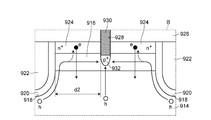
- one metal plug 930 having a relatively small diameter is formed between two trenches 918 adjacent to each other. Accordingly, the distance d2 between the trench 918 and the p + -type diffusion region 932 is relatively long when viewed in plan (see FIG. 18).
- the holes generated at the bottom of the trench 918 move a relatively long distance until they are extracted to the source electrode 934, and the base region 916 and Since a high potential difference easily occurs between the metal plug 930 and the parasitic npn transistor including the source region 924 (n-type), the base region 916 (p-type), and the drift layer 914 (n-type), it is easy to turn on. (See FIG. 18). Further, (2) the area of the “interface between the source region 924 and the base region 916” is increased and the holes of the base region 916 are likely to enter the source region 924. From this point of view, the parasitic npn transistor is turned on. (See FIG.
- the present invention has been made to solve the above-described problems, and an object of the present invention is to provide a power semiconductor device that satisfies the demand for cost reduction and downsizing of electronic devices and has a high breakdown resistance. To do. Moreover, it aims at providing the manufacturing method of such a power semiconductor device.
- a power semiconductor device of the present invention includes a low resistance semiconductor layer, a first conductivity type drift layer formed on the low resistance semiconductor layer, and a second conductivity type formed on a surface of the drift layer.
- An electrode electrically connected to the concentration diffusion region is provided.
- two trenches adjacent to each other is a concept including not only the case where the trenches are viewed as a whole but also the case where the trenches are adjacent to each other when viewed from a predetermined cross section. For example, even when the trenches are in a lattice shape and the trenches are connected to each other, when adjacent to each other when viewed from a predetermined cut surface, the two adjacent trenches It shall be included (see FIG. 10). Further, in this specification, “between two adjacent trenches” includes not only a straight line between trenches in a plan view but also a case where the position is slightly deviated from the straight line. .
- the first conductivity type high concentration diffusion region is between the two adjacent trenches and only between the trench and the metal plug closest to the trench. Preferably it is formed.
- the metal is preferably tungsten.
- the interval between the two adjacent gate electrodes is preferably 2.5 ⁇ m or more.
- the interval between the two adjacent gate electrodes is not less than 5 times the width of the metal plug.
- the contact hole is formed to a deeper position than a bottom surface of the first conductivity type high concentration diffusion region.
- the depth position of the deepest part of the base region is preferably in the range of 0.5 ⁇ m to 2.0 ⁇ m.
- the drift layer has a plurality of first conductivity type column regions and a plurality of second conductivity type column regions which are alternately formed along a predetermined direction.
- the power semiconductor device preferably has a super junction structure including the first conductivity type column region and the second conductivity type column region.
- a method for manufacturing a power semiconductor device is a method for manufacturing a power semiconductor device according to any one of the above [1] to [8], wherein the low resistance semiconductor layer And a semiconductor substrate preparation step of preparing a semiconductor substrate having a drift layer of the first conductivity type formed on the low-resistance semiconductor layer, a trench formation step of forming a plurality of trenches in the drift layer, A gate electrode forming step of forming a gate electrode in the trench through the gate insulating film after forming a gate insulating film on the peripheral surface; and a depth shallower than the bottom of the trench from the surface of the drift layer Forming a base region of a second conductivity type up to a position, and a first guide so that at least a part of the base region is exposed on the inner peripheral surface of the trench.
- a first conductive type high concentration diffusion region forming step for forming a high concentration diffusion region, and an interlayer insulating film for forming an interlayer insulating film covering at least the first conductive type high concentration diffusion region, the gate insulating film and the gate electrode Forming a contact hole, forming a contact hole so as to reach at least the base region through the interlayer insulating film between two adjacent trenches, and a bottom surface of the contact hole
- a metal plug forming step of forming a metal plug, and the base region and the first over the interlayer insulating film via the metal plug Characterized in that it comprises a conductivity type high concentration diffusion region and an electrode forming step of forming the second conductivity type high concentration diffusion region and electrically connected to the electrode in this order.
- the power semiconductor device and the method for manufacturing the power semiconductor device according to the present invention include two or more contact holes formed between two adjacent trenches so as to pass through the interlayer insulating film and reach at least the base region, And a metal plug in which a metal is filled in the contact hole.
- the distance d1 between the trench and the second conductivity type high-concentration diffusion region in plan view is shorter than the distance d2 in the power MOSFET 900 according to the background art (see FIG. 2). .
- a carrier for example, a hole
- a parasitic transistor including a first conductivity type high concentration diffusion region (for example, n-type), a base region (for example, p-type), and a drift layer (for example, n-type) It is difficult to turn on (parasitic npn transistor) (see FIG. 2).
- the power semiconductor device and the method for manufacturing the power semiconductor device according to the present invention satisfy the demand for cost reduction and downsizing of the electronic equipment and have a large breakdown resistance.
- two or more contact holes are formed between two adjacent trenches, and the inside of the contact hole is filled with metal. Therefore, contact resistance is reduced as compared with a case where a contact hole formed between two adjacent trenches and a metal plug filled with metal inside the contact hole are provided. It becomes possible to do.
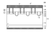
- FIG. 1 is a cross-sectional view of a power semiconductor device 100 according to Embodiment 1.
- FIG. 1 reference numeral 110 denotes a semiconductor substrate.
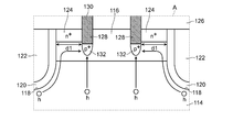
- the power semiconductor device 100 according to the first embodiment is shown to explain how holes are extracted to the source electrode 134 through the p + -type diffusion region 132 and the metal plug 130 at the time of avalanche breakdown and reverse recovery of the body diode. It is a principal part expanded sectional view. 2 corresponds to the area surrounded by the broken line A in FIG. In FIG. 2, white circles indicate holes. 6 is a cross-sectional view for explaining the method for manufacturing the power semiconductor device according to the first embodiment.
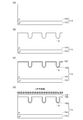
- 3A to 3D are process diagrams.
- FIG. 6 is a cross-sectional view for explaining the method for manufacturing the power semiconductor device according to the first embodiment.
- 4A to 4D are process diagrams. 6 is a cross-sectional view for explaining the method for manufacturing the power semiconductor device according to the first embodiment.
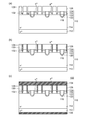
- FIG. 5A to FIG. 5D are process diagrams. 6 is a cross-sectional view for explaining the method for manufacturing the power semiconductor device according to the first embodiment.
- FIG. 6A to FIG. 6C are process diagrams.
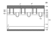
- FIG. 6 is a cross-sectional view of a power semiconductor device 102 according to a second embodiment.
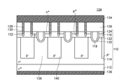
- FIG. 5 is a cross-sectional view of a power semiconductor device 104 according to a third embodiment.
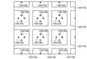
- FIG. 3 is an enlarged plan view of a main part of the power semiconductor device according to the power semiconductor device 100 according to Embodiment 1.
- FIG. in the power semiconductor device according to the first embodiment the trench 118 and the metal plug 130 are both striped when viewed in plan.
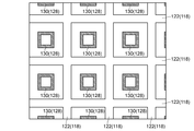
- 10 is an enlarged plan view of a main part of a power semiconductor device according to Modification 1.
- the trench 118 has a lattice shape when viewed in plan
- the metal plug 130 has a circular shape when viewed in plan (column shape when viewed in three dimensions).
- 10 is an enlarged plan view of a main part of a power semiconductor device according to Modification 2.
- FIG. 1 the trench 118 and the metal plug 130 are both striped when viewed in plan.
- 10 is an enlarged plan view of a main part of a power semiconductor device according to Modification 1.
- the trench 118 has a lattice shape when viewed in plan
- the metal plug 130 has a circular shape when viewed in plan (column shape when
- the trench 118 has a lattice shape when seen in a plan view
- the metal plug 130 has a rectangular frame shape when seen in a plan view.
- 10 is an enlarged plan view of a main part of a power semiconductor device according to Modification 3.
- FIG. 11 is an enlarged plan view of a main part of a power semiconductor device according to Modification 4.
- the trench 118 has a quadrangular shape (columnar shape when viewed three-dimensionally) when viewed in a plan view, and the metal plug 130 has a lattice shape when viewed in plan view.
- FIG. 10 is an enlarged plan view of a main part of a power semiconductor device according to Modification Example 5.
- the trench 118 has a quadrangular shape (columnar shape when viewed three-dimensionally) in plan view
- the metal plug 130 has a circular shape (viewed three-dimensionally) when viewed planarly. Columnar).
- FIG. 10 is a cross-sectional view of a power semiconductor device 106 according to Modification 6.
- FIG. 11 is a cross-sectional view of a power semiconductor device 108 according to Modification Example 7. It is sectional drawing of power MOSFET900 which concerns on background art. In the power MOSFET 900 according to the background art, an enlarged main portion is shown to explain how holes are extracted to the source electrode 934 through the p + -type diffusion region 932 and the metal plug 930 at the time of avalanche breakdown and reverse recovery of the body diode. It is sectional drawing. Note that FIG. 18 corresponds to a region surrounded by a broken line B in FIG. In FIG. 18, white circles indicate holes and black circles indicate electrons.
- Embodiment 1 Configuration of Power Semiconductor Device 100 According to Embodiment 1
- the power semiconductor device 100 according to Embodiment 1 is a trench gate power MOSFET used for various power supply devices such as a DC-DC converter.
- the breakdown voltage of the power semiconductor device 100 according to the first embodiment is 300V or more, for example, 600V.
- the power semiconductor device 100 includes a low-resistance semiconductor layer 112, an n ⁇ -type drift layer 114 formed on the low-resistance semiconductor layer 112, and a surface of the drift layer 114.
- the metal plug 130 thus formed, the p + type diffusion region 132 as the second conductivity type high concentration diffusion region having a higher impurity concentration than the base region 116 and being
- the trench 118, the gate electrode 122, the source region 124, the contact hole 128, and the metal plug 130 are all formed in a stripe shape when seen in a plan view.
- the interval between two adjacent gate electrodes 122 is at least five times the width (stripe width) of the metal plug 130.
- the interval (pitch width) between two gate electrodes 122 adjacent to each other is, for example, 2.5 ⁇ m or more, for example, 10 ⁇ m.
- the thickness of the low resistance semiconductor layer 112 is, for example, in the range of 100 ⁇ m to 400 ⁇ m, and the impurity concentration of the low resistance semiconductor layer 112 is, for example, in the range of 1 ⁇ 10 19 cm ⁇ 3 to 1 ⁇ 10 20 cm ⁇ 3. is there.
- the thickness of the drift layer 114 is, for example, in the range of 5 ⁇ m to 120 ⁇ m, and the impurity concentration of the drift layer 114 is, for example, in the range of 5 ⁇ 10 13 cm ⁇ 3 to 1 ⁇ 10 16 cm ⁇ 3 .
- the depth position of the deepest part of the base region 116 is within a range of 0.5 ⁇ m to 2.0 ⁇ m, for example, and the impurity concentration of the base region 116 is, for example, 5 ⁇ 10 16 cm ⁇ 3 to 1 ⁇ 10 18 cm ⁇ 3. It is in the range.
- the source region 124 is formed between two trenches 118 adjacent to each other only between the trench 118 and the metal plug 130 closest to the trench 118.
- the depth position of the deepest part of the source region 124 is, for example, in the range of 0.1 ⁇ m to 0.4 ⁇ m, and the impurity concentration of the source region 124 is, for example, 5 ⁇ 10 19 cm ⁇ 3 to 2 ⁇ 10 20 cm ⁇ 3. It is in the range.
- the depth of the trench 118 is, for example, 3 ⁇ m.
- the gate insulating film 120 is made of a silicon dioxide film formed by a thermal oxidation method, and has a thickness of, for example, 100 nm.
- the gate electrode 122 is made of low resistance polysilicon formed by a CVD method and an ion implantation method.
- the interlayer insulating film 126 is composed of a thermal oxide film and a PSG film formed by a CVD method, and has a thickness of, for example, 1000 nm.
- the contact hole 128 and the metal plug 130 are formed so as to reach a depth position deeper than the depth position of the bottom portion of the source region 124 from the depth position of the surface of the base region 116.
- the stripe width of the contact hole 128 and the metal plug 130 is, for example, 0.5 ⁇ m.
- a barrier metal (not shown) is formed on the inner surface of the contact hole 128, and the metal plug 130 is filled with metal inside the contact hole 128 through the barrier metal.
- the metal filling the contact hole 128 is, for example, tungsten.
- the metal plugs 130 are formed at an equally spaced pitch, and the interval between any one of the two trenches 118 and the metal plug 130 closest to the trench is as follows. , Equal to the interval between two metal plugs 130 adjacent to each other. With such a configuration, there is an effect that it is easy to alleviate the concentration of the electric field at the bottom of each trench 118 during reverse bias.
- the interval between the metal plugs 130 is equal to or longer than the stripe width of the metal plugs 130, for example, 0.5 ⁇ m or more.
- the deepest position of the p + -type diffusion region 132 is formed deeper than the source region 124.
- the impurity concentration of the p + -type diffusion region 132 is higher than the impurity concentration of the base region 116, for example, the 5 ⁇ 10 18 in the range of cm -3 ⁇ 1 ⁇ 10 20 cm -3.
- the source electrode 134 is made of an aluminum-based metal (for example, Al—Cu-based alloy) having a thickness of, for example, 4 ⁇ m formed by sputtering.
- the drain electrode 136 is formed of a multilayer metal film such as Ti—Ni—Au, and has a thickness of, for example, 0.5 ⁇ m over the entire multilayer metal film.
- the power semiconductor device 100 according to Embodiment 1 is manufactured by a manufacturing method (a manufacturing method of a power semiconductor device according to Embodiment 1) having manufacturing steps shown below. be able to.
- the semiconductor base 110 having the low resistance semiconductor layer 112 and the n ⁇ type drift layer 114 formed on the low resistance semiconductor layer 112 is prepared (see FIG. 3A).
- the semiconductor substrate 110 an appropriate semiconductor substrate can be used.
- a semiconductor substrate in which an n ⁇ type drift layer 114 is formed on an n + type low-resistance semiconductor layer 112 by an epitaxial growth method is used. it can.
- a mask (not shown) having an opening corresponding to the trench 118 is formed on the surface of the drift layer 114, and etching is performed using the mask, whereby the drift layer 114 is formed.
- a plurality of trenches 118 are formed (see FIG. 3B). After the etching, the mask is removed and the surface of the trench 118 is prepared by sacrificial oxidation.
- a thermal oxide film 120 ′ is formed by thermal oxidation on the surface of the drift layer 114 including the inner peripheral surface of the trench 118 (see FIG. 3C). At this time, the thermal oxide film on the inner peripheral surface of the trench 118 becomes the gate insulating film 120. Thereafter, polysilicon 122 ′ is deposited on the thermal oxide film 120 ′. Next, n-type impurities (for example, phosphorus) are ion-implanted into the entire surface of the polysilicon 122 ′ (see FIG. 3D) and thermally diffused. Next, the polysilicon is removed except for the inside of the trench 118. Thereby, the gate electrode 122 is formed inside the trench 118 via the gate insulating film 120 (see FIG. 4A).
- p-type impurities for example, boron
- the p-type impurity is thermally diffused to form a base region 116 from the surface of the drift layer 114 to a depth position shallower than the bottom of the trench 118 (see FIG. 4C).
- Source region 124 formation step (first conductivity type high concentration diffusion region formation step)
- a mask M1 having openings corresponding to the source region 124, the gate insulating film 120, and the gate electrode 122 is formed on the thermal oxide film 120 ′, and n-type impurities (for example, arsenic) are ion-implanted through the mask M1.
- n-type impurities for example, arsenic
- the source region 124 is formed on the surface of the base region 116 so as to be partially exposed on the inner peripheral surface of the trench 118 (see FIG. 5A).
- an interlayer insulating film 126 that covers the base region 116, the source region 124, the gate insulating film 120, and the gate electrode 122 is formed (see FIG. 5B). Specifically, a PSG film is formed on the thermal oxide film 120 ′ and the gate electrode 122 by a CVD method. Thus, an interlayer insulating film 126 composed of the thermal oxide film 120 ′ and the PSG film is formed.
- a mask (not shown) having two openings corresponding to the contact holes 128 is formed on the surface of the interlayer insulating film 126 between two adjacent trenches 118. .
- contact holes 128 are formed by performing etching so as to penetrate the interlayer insulating film 126 and reach the base region 116 using the mask. After the etching, the mask is removed (see FIG. 5C).
- Step of forming p + type diffusion region 132 (second conductivity type high concentration diffusion region formation step)
- p-type impurities for example, boron
- p + type diffusion region 132 formed in contact with the bottom surface of the contact hole 128 is formed by thermally diffusing the p type impurity. (See FIG. 6A.)
- a barrier metal (not shown) is formed on the inner surface of the contact hole 128 by sputtering, and the barrier metal is annealed.
- a tungsten film is formed on the barrier metal by a CVD method to fill the contact hole 128 with tungsten through the barrier metal.
- CMP chemical vapor deposition
- the tungsten is left only in the contact hole 128 to form the metal plug 130 (see FIG. 6B).
- TiN titanium nitride
- TiW titanium tungsten
- MoSi molybdenum silicon
- Source electrode 134 and drain electrode 136 Step of forming source electrode 134 and drain electrode 136
- an Al—Cu-based metal is formed on the interlayer insulating film 126 and the metal plug 130 by sputtering, and the source region 124 and the p + are formed via the metal plug 130.
- a source electrode 134 that is electrically connected to the mold diffusion region 132 is formed.
- a multilayer metal film such as Ti—Ni—Au is formed on the low resistance semiconductor layer 112 to form the drain electrode 136 (see FIG. 6C).
- the power semiconductor device 100 according to the first embodiment can be manufactured.
- the power semiconductor device 100 and the power semiconductor device manufacturing method according to the first embodiment at least the base region 116 penetrates through the interlayer insulating film 126. Since the contact hole 128 formed so as to reach and the metal plug 130 in which the contact hole 128 is filled with metal is provided, the source electrode is connected to the source region as in the case of the power MOSFET 900 according to the background art. It is not necessary to form a contact hole having a large diameter as in the case of a power semiconductor device in direct contact, and a miniaturized power semiconductor device can be obtained. As a result, the power semiconductor device 100 and the method for manufacturing the power semiconductor device according to the first embodiment can be a power semiconductor device that meets the demand for cost reduction and downsizing of electronic devices.
- the power semiconductor device 100 and the method for manufacturing the power semiconductor device according to the first embodiment are formed so as to penetrate at least the base region 116 through two interlayer insulating films 126 between two adjacent trenches 118.
- the contact hole 128 and a metal plug 130 filled with metal in the contact hole 128 are provided.
- the distance d1 between the trench 118 and the p + -type diffusion region 132 in plan view is shorter than the distance d2 in the power MOSFET 900 according to the background art (see FIG. 2).
- the holes generated at the bottom of the trench 118 move a relatively short distance before being extracted by the source electrode 134, and the base region 116 and Since a high potential difference is unlikely to occur with the metal plug 130, a parasitic npn transistor including the source region 124 (n-type), the base region 116 (p-type), and the drift layer 114 (n-type) is difficult to turn on. (See FIG. 2). Further, (2) since the area of “the boundary surface between the source region 124 and the base region 116” becomes narrow and the holes of the base region 116 do not easily enter the source region 124, the parasitic npn transistor described above is also turned on from this viewpoint.
- the power semiconductor device 100 and the method for manufacturing the power semiconductor device according to the first embodiment are unlikely to cause avalanche breakdown or di / dt breakdown, and can be a power semiconductor device having a large breakdown resistance.
- the power semiconductor device 100 and the method for manufacturing the power semiconductor device according to the first embodiment can satisfy the demand for cost reduction and downsizing of the electronic device and can be a power semiconductor device having a large breakdown resistance.
- two contact holes 128 are formed between two adjacent trenches 118, and a metal is formed inside the contact hole 128.
- a metal plug 130 filled with metal a contact hole formed between two adjacent trenches 118 and a metal plug filled with metal inside the contact hole are provided. As a result, the contact resistance can be reduced.
- the source region 124 is formed only between the trench 118 adjacent to each other and between the trench 118 and the metal plug 130 closest to the trench. Therefore, the area of the “boundary surface between the source region 124 and the base region 116” is narrowed and holes are less likely to enter the source region 124, so that the above-described parasitic npn transistor is less likely to be turned on.
- the metal is tungsten, it is easy to fill the contact hole 128 having a small diameter, and the metal plug 130 having a small diameter can be formed. It can be set as the power semiconductor device made.
- the gate electrode between the region with the interlayer insulating film and the region without the interlayer insulating film (contact region). If wire bonding is performed above, stress due to ultrasonic waves may concentrate on the step portion (particularly, the corner portion of the side surface of the interlayer insulating film (the boundary portion of the contact hole)), and the power semiconductor device may be destroyed.
- the metal is tungsten, and the contact hole 128 having a small diameter can be easily filled. Therefore, when the inside of the contact hole 128 is filled with tungsten, the interlayer is formed.
- the gate capacitance can be reduced.
- the amount of electric charge that the gate drive circuit (connected to the power semiconductor device 100) takes in and out of the gate electrode 122 during switching can be reduced, and drive loss can be reduced. That is, (1) at the time of turn-on, the gate drive circuit applies a positive bias to the gate electrode 122 to flow a gate current.
- the gate charge amount is obtained by multiplying the gate current amount by the energization time.
- the gate drive circuit applies a minus bias or 0 bias to the gate electrode 122 to draw out the gate current.
- the gate current amount is maintained at the same level as before and the energization time is shortened, the product of the gate current and the energization time can be reduced.
- the amount of electric charge that the drive circuit takes in and out of the gate electrode can be reduced. As a result, drive loss can be reduced.
- a large external gate resistor is inserted between the gate electrode 122 and the gate drive circuit in order to intentionally slow down the switching speed of the MOSFET and avoid ringing and noise in the circuit.
- the external gate resistor has an effect of reducing the gate current amount, and can increase the energization time and extend the switching time. Therefore, the gate charge amount that is the product of the gate current amount and the energization time remains small. As a result, drive loss can be reduced. Therefore, as described in the above (1) and (2), the amount of charge that the gate drive circuit takes in and out of the gate electrode 122 during switching can be reduced, and as a result, drive loss can be reduced.
- the gate electrode 122 and the gate drive circuit are not connected. Even when a large external gate resistor is inserted in the external gate resistor, the external gate resistor has an effect of reducing the gate current amount, and the energization time can be lengthened and the switching time can be extended. As a result, the switching speed becomes slow and the switching time becomes long, so that dv / dt becomes slow, and the occurrence of ringing and noise in the circuit can be avoided.
- the power semiconductor device 100 by reducing the gate capacitance, it is possible to widen the adjustment speed of the switching speed without losing the effect of reducing the drive loss, and as a result, from the application circuit. Can answer a wide range of requests.
- the interval between the two adjacent gate electrodes 122 is not less than five times the width of the metal plug 130, and the interval between the two adjacent gate electrodes 122 is Since it becomes wider with respect to the metal plug 130 and the volume of the gate electrode 122 can be made relatively small, this also makes it possible to reduce the gate capacitance. As a result, at the time of switching, the amount of charge that the gate drive circuit takes in and out of the gate electrode 122 can be reduced, and drive loss can be reduced.
- the distance between the two adjacent gate electrodes 122 is not less than five times the width of the metal plug 130, which also reduces the gate capacitance. As a result, it is possible to widen the adjustment speed of the switching speed without losing the effect of reducing the drive loss, and as a result, it is possible to respond widely to requests from the application circuit.
- the contact hole 128 is formed to a deeper position than the bottom surface of the source region 124, the p + type diffusion formed at the bottom of the contact hole 128.
- the impurity concentration and the region area of the source region 124 can be prevented from changing from the design time, and the problem that the characteristics of the power semiconductor device can be prevented can be prevented.
- the power semiconductor device 100 since the depth of the base region 116 is in the range of 0.5 ⁇ m to 2.0 ⁇ m, it is necessary to diffuse impurities at a high temperature for a long time in the manufacturing process. There is no. Therefore, the power semiconductor device is suitable when it is difficult to diffuse impurities for a long time in order to obtain a miniaturized structure.
- the power semiconductor device 102 according to the second embodiment basically has the same configuration as that of the power semiconductor device 100 according to the first embodiment, but the number of metal plugs is different from that of the power semiconductor device 100 according to the first embodiment. Different. That is, in the power semiconductor device 102 according to the second embodiment, as shown in FIG. 7, four contact holes 128 are formed between two adjacent trenches 118, respectively. Each contact hole 128 is filled with metal, and four metal plugs 130 are formed.
- the power semiconductor device 102 according to the second embodiment is different from the power semiconductor device 100 according to the first embodiment in the number of metal plugs, but is similar to the power semiconductor device 100 according to the first embodiment. Since the contact hole 128 formed so as to penetrate at least the base region 116 through the interlayer insulating film 126 and the metal plug 130 in which the metal is filled in the contact hole 128 is provided, the cost of the electronic device is reduced.
- the power semiconductor device satisfies the demands for downsizing and miniaturization and has a large breakdown resistance.
- each contact hole 128 is filled with metal. Since the metal plug 130 is formed, the depletion layer generated from the pn junction between the base region 116 and the drift layer 114 can be surely spread between the two adjacent trenches at the time of reverse bias. it can.
- the power semiconductor device 102 according to the second embodiment has the same configuration as that of the power semiconductor device 100 according to the first embodiment except for the number of metal plugs. Therefore, the power semiconductor device 100 according to the first embodiment includes the power semiconductor device 102 according to the first embodiment. It has a corresponding effect among the effects.
- the power semiconductor device 104 according to the third embodiment basically has the same configuration as that of the power semiconductor device 100 according to the first embodiment, but the power semiconductor device 104 according to the first embodiment has a super junction structure. Is different. That is, in the power semiconductor device 104 according to the third embodiment, as shown in FIG. 8, the drift layer 114 includes a plurality of n ⁇ -type column regions 138 and a plurality of p-type regions that are alternately formed along a predetermined direction.
- the power semiconductor device 104 according to the third embodiment has a super junction structure including a plurality of n ⁇ type column regions 138 and a plurality of p ⁇ type column regions 140.
- the p ⁇ -type column regions 140 are formed at predetermined intervals along a predetermined direction from the surface of the drift layer 114 on the base region 116 side.
- the p ⁇ -type column regions 140 and the n ⁇ -type column regions 138 formed of a part of the drift layer 114 where the p ⁇ -type column regions 140 are not formed are alternately arranged along a predetermined direction. It will be in the formed state.
- a region where the trench 118 is formed is formed in a region where the n ⁇ -type column region 138 is formed in plan view.
- the metal plug 130 is formed only in a region where the p ⁇ type column region 140 is formed in plan view, but the p ⁇ type column region 140 is formed. In addition to the region, it may be formed in a region where n ⁇ type column region 138 is formed in plan view.
- the n ⁇ -type column region 138 and the p ⁇ -type column region 140 have substantially the same width, and the n ⁇ -type column region 138 and the p ⁇ -type column region 140 have a charge balance. It is in a state that has been removed.
- the width of the n ⁇ -type column region 138 and the width of the p ⁇ -type column region 140 are each 6 ⁇ m, for example, and the impurity concentrations of the n ⁇ -type column region 138 and the p ⁇ -type column region 140 are each 5 ⁇ 10 14 cm, for example. -3 to 5 ⁇ 10 16 cm -3 .
- the power semiconductor device 104 according to the third embodiment is different from the power semiconductor device 100 according to the first embodiment in that it has a super junction structure, but the power semiconductor device 104 according to the first embodiment is different from the power semiconductor device 100 according to the first embodiment.
- a plurality of contact holes 128 that are formed so as to penetrate at least the base region 116 through the interlayer insulating film 126, and are formed between two adjacent trenches 118.
- the metal plug 130 filled in the contact hole 128 is provided, the power semiconductor device satisfies the demand for cost reduction and downsizing of the electronic device and has a large breakdown resistance.
- the drift layer 114 includes a plurality of n ⁇ -type column regions 138 and a plurality of p ⁇ -type column regions 140 that are alternately formed along a predetermined direction.
- the power semiconductor device 104 according to the third embodiment has a super junction structure composed of a plurality of n ⁇ -type column regions 138 and a plurality of p ⁇ -type column regions 140, and thus has an on-resistance while maintaining a high breakdown voltage. Can be lowered.
- the drift layer 114 includes a plurality of n ⁇ -type column regions 138 and a plurality of p ⁇ -type column regions 140 that are alternately formed along a predetermined direction.
- the power semiconductor device 104 according to the third embodiment has a super junction structure composed of a plurality of n ⁇ -type column regions 138 and a plurality of p ⁇ -type column regions 140, and thus has a high breakdown voltage. Even if it is a semiconductor device, it can be set as the power semiconductor device which satisfy
- the power semiconductor device 104 according to the third embodiment has the same configuration as that of the power semiconductor device 100 according to the first embodiment except that the power semiconductor device 104 has a super junction structure, and thus the power semiconductor device 100 according to the first embodiment. Has the corresponding effect among the effects of
- the metal plug 130 is formed in a stripe shape in plan view (see FIG. 9), but the present invention is not limited to this.
- the metal plug is circular (three-dimensionally columnar, see FIGS. 10 and 14), square frame (see FIG. 11), circular frame (see FIG. 12) or lattice. (See FIG. 13) or the like.
- the trench 118 is formed in a stripe shape when viewed in plan (see FIG. 9), but the present invention is not limited to this.
- the trench may be formed in a quadrangular shape (columnar shape, see FIGS. 13 and 14) or a lattice shape (see FIGS. 10, 11, and 12) or the like when viewed in plan.
- the present invention is applied to the trench gate power MOSFET, but the present invention is not limited to this.
- the present invention may be applied to a planar gate power MOSFET.
- the present invention is applied to a MOSFET, but the present invention is not limited to this.
- the present invention may be applied to an appropriate power semiconductor device such as an IGBT, a thyristor, a triac, or a diode.
- contact hole 128 is formed to reach the base region 116 in the third embodiment, the present invention is not limited to this.
- Contact hole 128 may be formed to reach p ⁇ type column region 140. In this case, there is an effect that holes can be easily extracted to the source electrode 134 at the time of avalanche breakdown and reverse recovery of the body diode.
- the p + -type diffusion region 132 is formed only at the bottom of the contact hole 128, but the present invention is not limited to this.
- the p + -type diffusion region 132 may be formed on a part of the side part (part on the bottom part side) in addition to the bottom part of the contact hole 128. In this case, it is possible to prevent the power semiconductor device from being destroyed by contact of the depletion layer with the contact plug at the time of avalanche breakdown and reverse recovery of the body diode.
- two contact holes 128 and two metal plugs 130 are formed between two trenches 118 adjacent to each other.
- the second embodiment between the two trenches 118 adjacent to each other.
- four contact holes 128 and four metal plugs 130 are formed in the first embodiment, the present invention is not limited to this. Three or five or more contact holes 128 and metal plugs 130 may be formed between two trenches 118 adjacent to each other.
- the source region 124 is formed only between the trench 118 adjacent to each other and between the trench 118 and the metal plug 130 closest to the trench. It is not limited. The source region 124 may be formed between the metal plugs 130 between two adjacent trenches 118 (see FIG. 15).
- the contact hole 128 is formed up to a depth position deeper than the bottom surface of the source region 124, but the present invention is not limited to this.
- the contact hole 128 may be formed to a depth position shallower than the bottom surface of the source region 124 (see FIG. 16).
Landscapes
- Electrodes Of Semiconductors (AREA)
- Chemical & Material Sciences (AREA)
- Composite Materials (AREA)
Abstract
本発明のパワー半導体装置100は、低抵抗半導体層112と、n-型のドリフト層114と、p型のベース領域116と、複数のトレンチ118と、ゲート絶縁膜120と、ゲート電極122と、n+型のソース領域124と、層間絶縁膜126と、互いに隣接する2つのトレンチ118の間にそれぞれ2本以上形成されたコンタクトホール128と、コンタクトホール128のそれぞれの内部に金属が充填されてなる金属プラグ130と、金属プラグ130の底面に接触してなるp+型拡散領域132と、層間絶縁膜126上に形成され、金属プラグ130を介してベース領域116、ソース領域124及びp+型拡散領域132に電気的に接続されたソース電極134とを備える。 本発明によれば、電子機器の低コスト化及び小型化の要請を満たし、かつ、破壊耐量の大きなパワー半導体装置を提供することができる。
Description
本発明は、パワー半導体装置及びパワー半導体装置の製造方法に関する。
近年、電子機器の低コスト化及び小型化の要請に伴い、微細化されたパワーMOSFETが求められている。そして、このようなパワーMOSFETとしては、金属プラグを介してソース電極とソース領域との間を電気的に接続するパワーMOSFETが考えられる(背景技術に係るパワーMOSFET900、図17参照。金属プラグを用いた半導体装置としては、例えば、特許文献1参照。)。
背景技術に係るパワーMOSFET900は、低抵抗半導体層912と、低抵抗半導体層912上に形成されたn-型のドリフト層914と、ドリフト層914の表面に形成されたp型のベース領域916と、ベース領域916を貫通しドリフト層914に達する深さ位置まで形成された複数のトレンチ918と、トレンチ918の内周面に形成されたゲート絶縁膜920と、ゲート絶縁膜920を介してトレンチ918の内部に埋め込まれてなるゲート電極922と、ベース領域916の表面に配置されるとともに少なくとも一部がトレンチ918の内周面に露出するように形成されたn+型のソース領域924と、ソース領域924、ゲート絶縁膜920及びゲート電極922を覆う層間絶縁膜926と、互いに隣接する2つのトレンチ918の間にそれぞれ1本、層間絶縁膜926を貫通して少なくともベース領域916に達するように形成されたコンタクトホール928と、コンタクトホール928の内部に金属が充填されてなる金属プラグ930と、金属プラグ930の底面に接触してなる、ベース領域916よりも不純物濃度が高いp+型拡散領域932と、層間絶縁膜926上に形成され、金属プラグ930を介してソース領域924及びp+型拡散領域932と電気的に接続されたソース電極934と、低抵抗半導体層912の表面の形成されたドレイン電極936とを備える。
背景技術に係るパワーMOSFET900によれば、層間絶縁膜926を貫通して少なくともベース領域916に達するように形成されたコンタクトホール928と、コンタクトホール928の内部に金属が充填されてなる金属プラグ930とを備えるため、ソース電極がソース領域と直接コンタクトされたパワー半導体装置の場合のように径が大きいコンタクトホールを形成しなくても済み、微細化されたパワーMOSFETとすることができる。その結果、背景技術に係るパワーMOSFET900は、電子機器の低コスト化及び小型化の要請に適うパワーMOSFETとなる。
しかしながら、背景技術に係るパワーMOSFET900においては、比較的径が小さい金属プラグ930が、互いに隣接する2つのトレンチ918の間にそれぞれ1本形成されている。
従って、平面的に見てトレンチ918とp+型拡散領域932との間隔d2が比較的長くなる(図18参照。)。よって、(1)アバランシェ降伏時及びボディダイオードの逆回復時において、トレンチ918の底部で発生したホールがソース電極934に引き抜かれるまでの間に比較的長い距離を移動することとなり、ベース領域916と金属プラグ930との間に高い電位差が発生しやすくなるため、ソース領域924(n型)、ベース領域916(p型)及びドリフト層914(n型)で構成される寄生npnトランジスタがオンしやすくなる(図18参照。)。また、(2)「ソース領域924とベース領域916との境界面」の面積が広くなりベース領域916のホールがソース領域924に入り込みやすくなるため、この観点においても、上記した寄生npnトランジスタがオンしやすくなる(図18参照。)。
その結果、アバランシェ破壊又はdi/dt破壊が起こりやすくなり、破壊耐量の大きなパワーMOSFETを提供することが困難となるという問題がある。なお、このような問題はパワーMOSFETの場合だけに発生し得る問題ではなく、パワー半導体装置全般に発生し得る問題である。
従って、平面的に見てトレンチ918とp+型拡散領域932との間隔d2が比較的長くなる(図18参照。)。よって、(1)アバランシェ降伏時及びボディダイオードの逆回復時において、トレンチ918の底部で発生したホールがソース電極934に引き抜かれるまでの間に比較的長い距離を移動することとなり、ベース領域916と金属プラグ930との間に高い電位差が発生しやすくなるため、ソース領域924(n型)、ベース領域916(p型)及びドリフト層914(n型)で構成される寄生npnトランジスタがオンしやすくなる(図18参照。)。また、(2)「ソース領域924とベース領域916との境界面」の面積が広くなりベース領域916のホールがソース領域924に入り込みやすくなるため、この観点においても、上記した寄生npnトランジスタがオンしやすくなる(図18参照。)。
その結果、アバランシェ破壊又はdi/dt破壊が起こりやすくなり、破壊耐量の大きなパワーMOSFETを提供することが困難となるという問題がある。なお、このような問題はパワーMOSFETの場合だけに発生し得る問題ではなく、パワー半導体装置全般に発生し得る問題である。
そこで、本発明は、上記した問題を解決するためになされたものであり、電子機器の低コスト化及び小型化の要請を満たし、かつ、破壊耐量の大きなパワー半導体装置を提供することを目的とする。また、そのようなパワー半導体装置の製造方法を提供することを目的とする。
[1]本発明のパワー半導体装置は、低抵抗半導体層と、前記低抵抗半導体層上に形成された第1導電型のドリフト層と、前記ドリフト層の表面に形成された第2導電型のベース領域と、前記ベース領域を貫通し前記ドリフト層に達する深さ位置まで形成された複数のトレンチと、前記トレンチの内周面に形成されたゲート絶縁膜と、前記ゲート絶縁膜を介して前記トレンチの内部に埋め込まれてなるゲート電極と、前記ベース領域の表面に配置されるとともに少なくとも一部が前記トレンチの内周面に露出するように形成された第1導電型高濃度拡散領域と、前記第1導電型高濃度拡散領域、前記ゲート絶縁膜及び前記ゲート電極を少なくとも覆う層間絶縁膜と、互いに隣接する2つの前記トレンチの間にそれぞれ2本以上、前記層間絶縁膜を貫通して少なくとも前記ベース領域に達するように形成されたコンタクトホールと、前記コンタクトホールの内部に金属が充填されてなる金属プラグと、前記金属プラグの底面に接触してなる、前記ベース領域よりも不純物濃度が高い第2導電型高濃度拡散領域と、前記層間絶縁膜上に形成され、前記金属プラグを介して前記ベース領域、前記第1導電型高濃度拡散領域及び前記第2導電型高濃度拡散領域と電気的に接続された電極とを備えることを特徴とする。
なお、本明細書中において、「互いに隣接する2つのトレンチ」とは、全体的に見ている場合のみならず、所定の断面から見てトレンチが隣り合っている場合を含む概念である。例えば、トレンチが格子状になっており、トレンチ同士が互いに連結されている場合であっても、所定の切断面で見たときに隣り合っている場合には「互いに隣接する2つのトレンチ」に含まれるものとする(図10参照。)。また、本明細書中において「互いに隣接する2つのトレンチの間」には、平面的に見てトレンチ同士の間の直線上だけではなく、当該直線上から多少ずれた位置にある場合も含むものとする。
[2]本発明のパワー半導体装置においては、前記第1導電型高濃度拡散領域は、互いに隣接する2つの前記トレンチの間において、前記トレンチと当該トレンチに最も近い前記金属プラグとの間のみに形成されていることが好ましい。
[3]本発明のパワー半導体装置においては、前記金属は、タングステンであることが好ましい。
[4]本発明のパワー半導体装置においては、互いに隣接する2つの前記ゲート電極の間隔は、2.5μm以上であることが好ましい。
[5]本発明のパワー半導体装置においては、互いに隣接する2つの前記ゲート電極の間隔は、前記金属プラグの幅の5倍以上であることが好ましい。
[6]本発明のパワー半導体装置においては、前記コンタクトホールは、前記第1導電型高濃度拡散領域の底面よりも深い深さ位置まで形成されていることが好ましい。
[7]本発明のパワー半導体装置においては、前記ベース領域の最深部の深さ位置は、0.5μm~2.0μmの範囲内にあることが好ましい。
[8]本発明のパワー半導体装置においては、前記ドリフト層は、所定の方向に沿って交互に形成されている複数の第1導電型コラム領域及び複数の第2導電型コラム領域を有し、前記パワー半導体装置は、前記第1導電型コラム領域及び前記第2導電型コラム領域で構成されたスーパージャンクション構造を有することが好ましい。
[9]本発明のパワー半導体装置の製造方法は、上記[1]~[8]のいずれかに記載のパワー半導体装置を製造するためのパワー半導体装置の製造方法であって、低抵抗半導体層及び前記低抵抗半導体層上に形成された第1導電型のドリフト層を有する半導体基体を準備する半導体基体準備工程と、前記ドリフト層に複数のトレンチを形成するトレンチ形成工程と、前記トレンチの内周面にゲート絶縁膜を形成した後、前記ゲート絶縁膜を介して前記トレンチの内部にゲート電極を形成するゲート電極形成工程と、前記ドリフト層の表面から前記トレンチの最底部よりも浅い深さ位置まで第2導電型のベース領域を形成するベース領域形成工程と、前記ベース領域の表面に、少なくとも一部が前記トレンチの内周面に露出するように第1導電型高濃度拡散領域を形成する第1導電型高濃度拡散領域形成工程と、前記第1導電型高濃度拡散領域、前記ゲート絶縁膜及び前記ゲート電極を少なくとも覆う層間絶縁膜を形成する層間絶縁膜形成工程と、互いに隣接する2つの前記トレンチ間にそれぞれ2本以上、前記層間絶縁膜を貫通して少なくとも前記ベース領域に達するようにコンタクトホールを形成するコンタクトホール形成工程と、前記コンタクトホールの底面に接触してなる、前記ベース領域よりも不純物濃度が高い第2導電型高濃度拡散領域を形成する第2導電型高濃度拡散領域形成工程と、前記コンタクトホールの内部に金属を充填することによって金属プラグを形成する金属プラグ形成工程と、前記層間絶縁膜上に、前記金属プラグを介して前記ベース領域、前記第1導電型高濃度拡散領域及び前記第2導電型高濃度拡散領域と電気的に接続された電極を形成する電極形成工程とをこの順序で含むことを特徴とする。
本発明のパワー半導体装置及びパワー半導体装置の製造方法によれば、層間絶縁膜を貫通して少なくともベース領域に達するように形成されたコンタクトホールと、コンタクトホールの内部に金属が充填されてなる金属プラグとを備えるため、背景技術に係るパワーMOSFET900の場合と同様に、ソース電極がソース領域と直接コンタクトしているパワー半導体装置の場合のように径が大きいコンタクトホールを形成しなくても済み、微細化されたパワー半導体装置とすることができる。その結果、本発明のパワー半導体装置は、電子機器の低コスト化及び小型化の要請に適うパワー半導体装置となる。
本発明のパワー半導体装置及びパワー半導体装置の製造方法は、互いに隣接する2つのトレンチの間にそれぞれ2本以上、層間絶縁膜を貫通して少なくともベース領域に達するように形成されたコンタクトホールと、コンタクトホールの内部に金属が充填されてなる金属プラグとを備える。
このような構成としたことにより、平面的に見てトレンチと第2導電型高濃度拡散領域との間隔d1が、背景技術に係るパワーMOSFET900における当該間隔d2よりも短くなる(図2参照。)。従って、(1)アバランシェ降伏時及びディダイオードの逆回復時において、トレンチの底部で発生したキャリア(例えばホール)が電極に引き抜かれるまでの間に比較的短い距離を移動することとなり、ベース領域と金属プラグとの間に高い電位差が発生し難くなるため、第1導電型高濃度拡散領域(例えばn型)、ベース領域(例えばp型)及びドリフト層(例えばn型)で構成される寄生トランジスタ(寄生npnトランジスタ)がオンし難くなる(図2参照。)。また、(2)「第1導電型高濃度拡散領域とベース領域との境界面」の面積が狭くなりベース領域のキャリア(例えばホール)が第1導電型高濃度拡散領域に入り込み難くなるため、この観点においても、上記した寄生トランジスタ(寄生npnトランジスタ)がオンし難くなる(図2参照。)。
その結果、アバランシェ破壊又はdi/dt破壊が起こり難くなり、破壊耐量の大きなパワー半導体装置となる。
このような構成としたことにより、平面的に見てトレンチと第2導電型高濃度拡散領域との間隔d1が、背景技術に係るパワーMOSFET900における当該間隔d2よりも短くなる(図2参照。)。従って、(1)アバランシェ降伏時及びディダイオードの逆回復時において、トレンチの底部で発生したキャリア(例えばホール)が電極に引き抜かれるまでの間に比較的短い距離を移動することとなり、ベース領域と金属プラグとの間に高い電位差が発生し難くなるため、第1導電型高濃度拡散領域(例えばn型)、ベース領域(例えばp型)及びドリフト層(例えばn型)で構成される寄生トランジスタ(寄生npnトランジスタ)がオンし難くなる(図2参照。)。また、(2)「第1導電型高濃度拡散領域とベース領域との境界面」の面積が狭くなりベース領域のキャリア(例えばホール)が第1導電型高濃度拡散領域に入り込み難くなるため、この観点においても、上記した寄生トランジスタ(寄生npnトランジスタ)がオンし難くなる(図2参照。)。
その結果、アバランシェ破壊又はdi/dt破壊が起こり難くなり、破壊耐量の大きなパワー半導体装置となる。
従って、本発明のパワー半導体装置及びパワー半導体装置の製造方法は、電子機器の低コスト化及び小型化の要請を満たし、かつ、破壊耐量の大きなパワー半導体装置となる。
また、本発明のパワー半導体装置及びパワー半導体装置の製造方法によれば、互いに隣接する2つのトレンチの間にそれぞれ2本以上形成されたコンタクトホールと、当該コンタクトホールの内部に金属が充填されてなる金属プラグとを備えるため、互いに隣接する2つのトレンチの間にそれぞれ1本形成されたコンタクトホールと、コンタクトホールの内部に金属が充填されてなる金属プラグとを備える場合よりもコンタクト抵抗を低減することが可能となる。
以下、本発明のパワー半導体装置及びパワー半導体装置の製造方法について、図に示す実施の形態に基づいて説明する。なお、各図面は模式図であり、必ずしも実際の寸法を厳密に反映したものではない。
[実施形態1]
1.実施形態1に係るパワー半導体装置100の構成
実施形態1に係るパワー半導体装置100は、DC-DCコンバーターなど各種電源装置等に用いられるトレンチゲートパワーMOSFETである。実施形態1に係るパワー半導体装置100の耐圧は、300V以上であり、例えば600Vである。
1.実施形態1に係るパワー半導体装置100の構成
実施形態1に係るパワー半導体装置100は、DC-DCコンバーターなど各種電源装置等に用いられるトレンチゲートパワーMOSFETである。実施形態1に係るパワー半導体装置100の耐圧は、300V以上であり、例えば600Vである。
実施形態1に係るパワー半導体装置100は、図1に示すように、低抵抗半導体層112と、低抵抗半導体層112上に形成されたn-型のドリフト層114と、ドリフト層114の表面に形成されたp型のベース領域116と、ベース領域116を貫通しドリフト層114に達する深さ位置まで形成された複数のトレンチ118と、トレンチ118の内周面に形成されたゲート絶縁膜120と、ゲート絶縁膜120を介してトレンチ118の内部に埋め込まれてなるゲート電極122と、ベース領域116の表面に配置されるとともに一部がトレンチ118の内周面に露出するように形成されたn+型の第1導電型高濃度拡散領域としてのソース領域124と、ソース領域124、ゲート絶縁膜120及びゲート電極122を覆う層間絶縁膜126と、互いに隣接する2つのトレンチ118の間にそれぞれ2本、層間絶縁膜126を貫通してベース領域116に達するように形成されたコンタクトホール128と、コンタクトホール128の内部に金属が充填されてなる金属プラグ130と、金属プラグ130の底面に接触してなる、ベース領域116よりも不純物濃度が高い第2導電型高濃度拡散領域としてのp+型拡散領域132と、層間絶縁膜126上に形成され、金属プラグ130を介してベース領域116、ソース領域124及びp+型拡散領域132と電気的に接続された電極としてのソース電極134と、低抵抗半導体層112の表面の形成されたドレイン電極136とを備える。
実施形態1に係るパワー半導体装置100において、トレンチ118、ゲート電極122、ソース領域124、コンタクトホール128及び金属プラグ130はいずれも、平面的に見てストライプ状に形成されている。互いに隣接する2つのゲート電極122の間隔は、金属プラグ130の幅(ストライプ幅)の5倍以上である。具体的には、互いに隣接する2つのゲート電極122の間隔(ピッチ幅)は、例えば2.5μm以上であり、例えば10μmである。
低抵抗半導体層112の厚さは、例えば100μm~400μmの範囲内にあり、低抵抗半導体層112の不純物濃度は、例えば1×1019cm-3~1×1020cm-3の範囲内にある。ドリフト層114の厚さは、例えば5μm~120μmの範囲内にあり、ドリフト層114の不純物濃度は例えば5×1013cm-3~1×1016cm-3の範囲内にある。ベース領域116の最深部の深さ位置は、例えば0.5μm~2.0μmの範囲内にあり、ベース領域116の不純物濃度は、例えば5×1016cm-3~1×1018cm-3の範囲内にある。
ソース領域124は、互いに隣接する2つのトレンチ118の間において、トレンチ118と当該トレンチ118に最も近い金属プラグ130との間のみに形成されている。ソース領域124の最深部の深さ位置は、例えば0.1μm~0.4μmの範囲内にあり、ソース領域124の不純物濃度は、例えば5×1019cm-3~2×1020cm-3の範囲内にある。
トレンチ118の深さは、例えば3μmである。ゲート絶縁膜120は、熱酸化法により形成された二酸化珪素膜からなり、厚さは例えば100nmである。ゲート電極122は、CVD法及びイオン注入法により形成された低抵抗ポリシリコンからなる。層間絶縁膜126は、熱酸化膜とCVD法により形成されたPSG膜とで構成され、厚さは例えば1000nmである。
コンタクトホール128及び金属プラグ130は、ベース領域116の表面の深さ位置からソース領域124の底部の深さ位置よりも深い深さ位置に達するように形成されている。コンタクトホール128及び金属プラグ130のストライプ幅は、例えば0.5μmである。
コンタクトホール128の内表面には、バリアメタル(図示せず)が形成されており、金属プラグ130は、当該バリアメタルを介して金属がコンタクトホール128の内部に充填されている。コンタクトホール128の内部に充填する金属は、例えばタングステンである。
互いに隣接する2つのトレンチ118の間において、金属プラグ130は、等間隔のピッチで形成されており、2つのトレンチ118のうちのいずれかのトレンチと当該トレンチに最も近い金属プラグ130との間隔は、互いに隣接する2つの金属プラグ130の間隔と等しい。このような構成とすることにより、逆バイアス時において、各トレンチ118において底部に電界が集中することを緩和しやすくなる、という効果がある。
金属プラグ130の間隔は、金属プラグ130のストライプ幅と同じ長さ又はそれ以上の長さであり、例えば0.5μm以上である。
金属プラグ130の間隔は、金属プラグ130のストライプ幅と同じ長さ又はそれ以上の長さであり、例えば0.5μm以上である。
p+型拡散領域132の最深部の深さ位置は、ソース領域124よりも深くなるように形成されている。p+型拡散領域132の不純物濃度は、ベース領域116の不純物濃度よりも高く、例えば5×1018cm-3~1×1020cm-3の範囲内にある。
ソース電極134は、スパッタ法により形成された厚さが例えば4μmのアルミニウム系の金属(例えば、Al-Cu系の合金)からなる。ドレイン電極136は、Ti-Ni-Auなどの多層金属膜により形成され、厚さが例えば多層金属膜全体にて0.5μmで形成されている。
2.実施形態1に係るパワー半導体装置の製造方法
次に、実施形態1に係るパワー半導体装置100は、以下に示す製造工程を有する製造方法(実施形態1に係るパワー半導体装置の製造方法)により製造することができる。
次に、実施形態1に係るパワー半導体装置100は、以下に示す製造工程を有する製造方法(実施形態1に係るパワー半導体装置の製造方法)により製造することができる。
(1)半導体基体110準備工程
まず、低抵抗半導体層112及び低抵抗半導体層112上に形成されたn-型のドリフト層114を有する半導体基体110を準備する(図3(a)参照。)。半導体基体110としては、適宜の半導体基体を用いることができるが、例えばn+型の低抵抗半導体層112上にエピタキシャル成長法によってn-型のドリフト層114を形成してなる半導体基体を用いることができる。
まず、低抵抗半導体層112及び低抵抗半導体層112上に形成されたn-型のドリフト層114を有する半導体基体110を準備する(図3(a)参照。)。半導体基体110としては、適宜の半導体基体を用いることができるが、例えばn+型の低抵抗半導体層112上にエピタキシャル成長法によってn-型のドリフト層114を形成してなる半導体基体を用いることができる。
(2)トレンチ118形成工程
次に、トレンチ118に対応する開口を有するマスク(図示せず。)をドリフト層114の表面に形成し、当該マスクを用いてエッチングを行うことにより、ドリフト層114に複数のトレンチ118を形成する(図3(b)参照。)。エッチング後、マスクを除去し、犠牲酸化によりトレンチ118の表面を整える。
次に、トレンチ118に対応する開口を有するマスク(図示せず。)をドリフト層114の表面に形成し、当該マスクを用いてエッチングを行うことにより、ドリフト層114に複数のトレンチ118を形成する(図3(b)参照。)。エッチング後、マスクを除去し、犠牲酸化によりトレンチ118の表面を整える。
(3)ゲート電極122形成工程
次に、トレンチ118の内周面を含むドリフト層114の表面上に熱酸化により熱酸化膜120’を形成する(図3(c)参照。)。このとき、トレンチ118の内周面の熱酸化膜がゲート絶縁膜120となる。その後、当該熱酸化膜120’上にポリシリコン122’を堆積させる。次に、当該ポリシリコン122’全面にn型不純物(例えば、リン)をイオン注入し(図3(d)参照。)、熱拡散させる。次に、トレンチ118の内部を除いてポリシリコンを除去する。これにより、トレンチ118の内部にゲート絶縁膜120を介してゲート電極122を形成する(図4(a)参照。)。
次に、トレンチ118の内周面を含むドリフト層114の表面上に熱酸化により熱酸化膜120’を形成する(図3(c)参照。)。このとき、トレンチ118の内周面の熱酸化膜がゲート絶縁膜120となる。その後、当該熱酸化膜120’上にポリシリコン122’を堆積させる。次に、当該ポリシリコン122’全面にn型不純物(例えば、リン)をイオン注入し(図3(d)参照。)、熱拡散させる。次に、トレンチ118の内部を除いてポリシリコンを除去する。これにより、トレンチ118の内部にゲート絶縁膜120を介してゲート電極122を形成する(図4(a)参照。)。
(4)ベース領域116形成工程
次に、ドリフト層114の表面に熱酸化膜120’を介してp型不純物(例えばボロン)をイオン注入する(図4(b)参照。)。次に、当該p型不純物を熱拡散させてドリフト層114の表面からトレンチ118の最底部よりも浅い深さ位置までベース領域116を形成する(図4(c)参照。)。
次に、ドリフト層114の表面に熱酸化膜120’を介してp型不純物(例えばボロン)をイオン注入する(図4(b)参照。)。次に、当該p型不純物を熱拡散させてドリフト層114の表面からトレンチ118の最底部よりも浅い深さ位置までベース領域116を形成する(図4(c)参照。)。
(5)ソース領域124形成工程(第1導電型高濃度拡散領域形成工程)
次に、ソース領域124、ゲート絶縁膜120及びゲート電極122に対応する開口を有するマスクM1を熱酸化膜120’上に形成し、当該マスクM1を介してn型不純物(例えばヒ素)をイオン注入する(図4(d)参照。)。次に、当該n型不純物を熱拡散することにより、ベース領域116の表面に、一部がトレンチ118の内周面に露出するようにソース領域124を形成する(図5(a)参照。)。
次に、ソース領域124、ゲート絶縁膜120及びゲート電極122に対応する開口を有するマスクM1を熱酸化膜120’上に形成し、当該マスクM1を介してn型不純物(例えばヒ素)をイオン注入する(図4(d)参照。)。次に、当該n型不純物を熱拡散することにより、ベース領域116の表面に、一部がトレンチ118の内周面に露出するようにソース領域124を形成する(図5(a)参照。)。
(6)層間絶縁膜126形成工程
次に、ベース領域116、ソース領域124、ゲート絶縁膜120及びゲート電極122を覆う層間絶縁膜126を形成する(図5(b)参照。)。具体的には、熱酸化膜120’及びゲート電極122上にCVD法によりPSG膜を形成する。これにより、熱酸化膜120’及びPSG膜で構成された層間絶縁膜126を形成する。
次に、ベース領域116、ソース領域124、ゲート絶縁膜120及びゲート電極122を覆う層間絶縁膜126を形成する(図5(b)参照。)。具体的には、熱酸化膜120’及びゲート電極122上にCVD法によりPSG膜を形成する。これにより、熱酸化膜120’及びPSG膜で構成された層間絶縁膜126を形成する。
(7)コンタクトホール128形成工程
次に、互いに隣接する2つのトレンチ118間にそれぞれ2つずつコンタクトホール128に対応する開口を有するマスク(図示せず。)を層間絶縁膜126の表面に形成する。次に、当該マスクを用いて層間絶縁膜126を貫通してベース領域116に達するようにエッチングを行うことによりコンタクトホール128を形成する。エッチング後、マスクを
除去する(図5(c)参照。)。
次に、互いに隣接する2つのトレンチ118間にそれぞれ2つずつコンタクトホール128に対応する開口を有するマスク(図示せず。)を層間絶縁膜126の表面に形成する。次に、当該マスクを用いて層間絶縁膜126を貫通してベース領域116に達するようにエッチングを行うことによりコンタクトホール128を形成する。エッチング後、マスクを
除去する(図5(c)参照。)。
(8)p+型拡散領域132形成工程(第2導電型高濃度拡散領域形成工程)
次に、コンタクトホール128の底面に、ベース領域116よりも高い不純物濃度でp型不純物(例えばボロン)をイオン注入する(図5(d)参照。)。次に、当該p型不純物を熱拡散しすることにより、コンタクトホール128の底面に接触してなるp+型拡散領域132を形成する。(図6(a)参照。)。
次に、コンタクトホール128の底面に、ベース領域116よりも高い不純物濃度でp型不純物(例えばボロン)をイオン注入する(図5(d)参照。)。次に、当該p型不純物を熱拡散しすることにより、コンタクトホール128の底面に接触してなるp+型拡散領域132を形成する。(図6(a)参照。)。
(9)金属プラグ130充填工程
次に、スパッタ法によりコンタクトホール128の内側面にバリアメタル(図示せず。)を成膜し、当該バリアメタルをアニールする。次にCVD法により当該バリアメタル上にタングステンを成膜することにより、コンタクトホール128の内部に当該バリアメタルを介してタングステンを充填する。次に、CMP法によって層間絶縁膜126上のタングステンを除去することにより、コンタクトホール128の内部にのみタングステンを残し、金属プラグ130を形成する(図6(b)参照。)。なお、バリアメタルの組成としては、チタンナイトライド(TiN)、チタンタングステン(TiW)、モリブデンシリコン(MоSi)等を用いることができる。
次に、スパッタ法によりコンタクトホール128の内側面にバリアメタル(図示せず。)を成膜し、当該バリアメタルをアニールする。次にCVD法により当該バリアメタル上にタングステンを成膜することにより、コンタクトホール128の内部に当該バリアメタルを介してタングステンを充填する。次に、CMP法によって層間絶縁膜126上のタングステンを除去することにより、コンタクトホール128の内部にのみタングステンを残し、金属プラグ130を形成する(図6(b)参照。)。なお、バリアメタルの組成としては、チタンナイトライド(TiN)、チタンタングステン(TiW)、モリブデンシリコン(MоSi)等を用いることができる。
(10)ソース電極134及びドレイン電極136形成工程
次に、スパッタ法により層間絶縁膜126及び金属プラグ130上にAl-Cu系金属を成膜し、金属プラグ130を介してソース領域124及びp+型拡散領域132と電気的に接続するソース電極134を形成する。また、低抵抗半導体層112上にTi-Ni-Auなどの多層金属膜を成膜し、ドレイン電極136を形成する(図6(c)参照。)。
次に、スパッタ法により層間絶縁膜126及び金属プラグ130上にAl-Cu系金属を成膜し、金属プラグ130を介してソース領域124及びp+型拡散領域132と電気的に接続するソース電極134を形成する。また、低抵抗半導体層112上にTi-Ni-Auなどの多層金属膜を成膜し、ドレイン電極136を形成する(図6(c)参照。)。
このようにして実施形態1に係るパワー半導体装置100を製造することができる。
3.実施形態1に係るパワー半導体装置100及びパワー半導体装置の製造方法の効果
実施形態1に係るパワー半導体装置100及びパワー半導体装置の製造方法によれば、層間絶縁膜126を貫通して少なくともベース領域116に達するように形成されたコンタクトホール128と、コンタクトホール128の内部に金属が充填されてなる金属プラグ130とを備えるため、背景技術に係るパワーMOSFET900の場合と同様に、ソース電極がソース領域と直接コンタクトしているパワー半導体装置の場合のように径が大きいコンタクトホールを形成しなくても済み、微細化されたパワー半導体装置とすることができる。その結果、実施形態1に係るパワー半導体装置100及びパワー半導体装置の製造方法は、電子機器の低コスト化及び小型化の要請に適うパワー半導体装置とすることができる。
実施形態1に係るパワー半導体装置100及びパワー半導体装置の製造方法によれば、層間絶縁膜126を貫通して少なくともベース領域116に達するように形成されたコンタクトホール128と、コンタクトホール128の内部に金属が充填されてなる金属プラグ130とを備えるため、背景技術に係るパワーMOSFET900の場合と同様に、ソース電極がソース領域と直接コンタクトしているパワー半導体装置の場合のように径が大きいコンタクトホールを形成しなくても済み、微細化されたパワー半導体装置とすることができる。その結果、実施形態1に係るパワー半導体装置100及びパワー半導体装置の製造方法は、電子機器の低コスト化及び小型化の要請に適うパワー半導体装置とすることができる。
実施形態1に係るパワー半導体装置100及びパワー半導体装置の製造方法は、互いに隣接する2つのトレンチ118の間にそれぞれ2本、層間絶縁膜126を貫通して少なくともベース領域116に達するように形成されたコンタクトホール128と、コンタクトホール128の内部に金属が充填されてなる金属プラグ130とを備える。
このような構成としたことにより、平面的に見てトレンチ118とp+型拡散領域132との間隔d1が、背景技術に係るパワーMOSFET900における当該間隔d2よりも短くなる(図2参照。)。従って、(1)アバランシェ降伏時及びボディダイオードの逆回復時において、トレンチ118の底部で発生したホールがソース電極134に引き抜かれるまでの間に比較的短い距離を移動することとなり、ベース領域116と金属プラグ130との間に高い電位差が発生し難くなるため、ソース領域124(n型)、ベース領域116(p型)及びドリフト層114(n型)で構成される寄生npnトランジスタがオンし難くなる(図2参照。)。また、(2)「ソース領域124とベース領域116との境界面」の面積が狭くなりベース領域116のホールがソース領域124に入り込み難くなるため、この観点においても、上記した寄生npnトランジスタがオンし難くなる(図2参照。)。
その結果、実施形態1に係るパワー半導体装置100及びパワー半導体装置の製造方法は、アバランシェ破壊又はdi/dt破壊が起こり難くなり、破壊耐量の大きなパワー半導体装置とすることができる。
このような構成としたことにより、平面的に見てトレンチ118とp+型拡散領域132との間隔d1が、背景技術に係るパワーMOSFET900における当該間隔d2よりも短くなる(図2参照。)。従って、(1)アバランシェ降伏時及びボディダイオードの逆回復時において、トレンチ118の底部で発生したホールがソース電極134に引き抜かれるまでの間に比較的短い距離を移動することとなり、ベース領域116と金属プラグ130との間に高い電位差が発生し難くなるため、ソース領域124(n型)、ベース領域116(p型)及びドリフト層114(n型)で構成される寄生npnトランジスタがオンし難くなる(図2参照。)。また、(2)「ソース領域124とベース領域116との境界面」の面積が狭くなりベース領域116のホールがソース領域124に入り込み難くなるため、この観点においても、上記した寄生npnトランジスタがオンし難くなる(図2参照。)。
その結果、実施形態1に係るパワー半導体装置100及びパワー半導体装置の製造方法は、アバランシェ破壊又はdi/dt破壊が起こり難くなり、破壊耐量の大きなパワー半導体装置とすることができる。
従って、実施形態1に係るパワー半導体装置100及びパワー半導体装置の製造方法は、電子機器の低コスト化及び小型化の要請を満たし、かつ、破壊耐量の大きなパワー半導体装置とすることができる。
また、実施形態1に係るパワー半導体装置100及びパワー半導体装置の製造方法によれば、互いに隣接する2つのトレンチ118の間にそれぞれ2本形成されたコンタクトホール128と、コンタクトホール128の内部に金属が充填されてなる金属プラグ130とを備えるため、互いに隣接する2つのトレンチ118の間にそれぞれ1本形成されたコンタクトホールと、コンタクトホールの内部に金属が充填されてなる金属プラグとを備える場合よりもコンタクト抵抗を低減することが可能となる。
また、実施形態1に係るパワー半導体装置100によれば、ソース領域124は、互いに隣接する2つのトレンチ118の間においてトレンチ118と当該トレンチに最も近い金属プラグ130との間のみに形成されているため、「ソース領域124とベース領域116との境界面」の面積が狭くなりホールがソース領域124により一層入り込み難くなるため、上記した寄生npnトランジスタがより確実にオンし難くなる。
また、実施形態1に係るパワー半導体装置100によれば、金属は、タングステンであるため、径が小さいコンタクトホール128内に充填しやすく、径が小さい金属プラグ130を形成することができ、微細化されたパワー半導体装置とすることができる。
ところで、ソース電極がソース領域と直接コンタクトされたパワー半導体装置においては、層間絶縁膜がある領域と層間絶縁膜がない領域(コンタクトの領域)とでゲート電極に段差ができるため、実装時にソース電極上でワイヤボンディングすると、当該段差部分(特に、層間絶縁膜の側面(コンタクトホールの境界部分)の角部)に超音波による応力が集中してパワー半導体装置が破壊されるおそれがある。これに対して、実施形態1に係るパワー半導体装置100によれば、金属は、タングステンであり、径が小さいコンタクトホール128内に充填しやすいことから、コンタクトホール128の内部をタングステンで充填すると層間絶縁膜126がある領域と層間絶縁膜126がない領域(金属プラグ130の領域)とで段差ができにくく、ソース電極134を平らに成膜することができる。従って、実装時にソース電極134上でワイヤボンディングしても、層間絶縁膜126の一部に超音波による応力が集中することを防ぐことができるため、パワー半導体装置が破壊されることを防ぐことができる。
また、実施形態1に係るパワー半導体装置100によれば、互いに隣接する2つのゲート電極122の間隔が2.5μm以上であるため、ゲート容量を小さくすることができる。その結果、スイッチングの際、(パワー半導体装置100と接続される)ゲートドライブ回路がゲート電極122に対して出し入れする電荷量を減らすことができ、ドライブ損失を低減することができる。
すなわち、(1)ターンオンの際には、ゲートドライブ回路は、ゲート電極122に対しプラスバイアスを与え、ゲート電流を流し込む。ゲート電流量に通電時間を掛け算すると、ゲート電荷量となる。ゲート容量が小さくなるとゲート電荷量が減るため、ゲート電流量と通電時間の積が小さくて済むことになる。その結果、ゲート電流量を減らすか、通電時間を短くするか、いずれかが可能となり、結果的に、ドライブ回路側の電力損失を低減することができる。
また、(2)ターンオフの際は、ゲートドライブ回路は、ゲート電極122に対しマイナスバイアスまたは0バイアスを与え、ゲート電流を引き抜く。このとき、(a)ゲート電荷量が少なくなったとき、ゲート電流量を以前と同等に維持して、通電時間を短くした場合には、ゲート電流と通電時間の積が小さくて済むため、ゲートドライブ回路がゲート電極に対して出し入れする電荷量を減らすことができる。その結果、ドライブ損失を低減することができる。また、(b)MOSFETのスイッチング速度を意図的に遅くし、回路にリンギングやノイズが発生するのを避けるために、ゲート電極122とゲートドライブ回路との間に大きめの外付けゲート抵抗を挿入した場合でも、当該外付けゲート抵抗は、ゲート電流量を絞る効果があり、通電時間を長くし、スイッチング時間を引き延ばすことができることから、ゲート電流量と通電時間の積であるゲート電荷量は小さいままであり、その結果、ドライブ損失を低減することができる。
従って、上記(1)及び(2)で記載したように、スイッチングの際、ゲートドライブ回路がゲート電極122に対して出し入れする電荷量を減らすことができ、その結果、ドライブ損失を低減できる。
すなわち、(1)ターンオンの際には、ゲートドライブ回路は、ゲート電極122に対しプラスバイアスを与え、ゲート電流を流し込む。ゲート電流量に通電時間を掛け算すると、ゲート電荷量となる。ゲート容量が小さくなるとゲート電荷量が減るため、ゲート電流量と通電時間の積が小さくて済むことになる。その結果、ゲート電流量を減らすか、通電時間を短くするか、いずれかが可能となり、結果的に、ドライブ回路側の電力損失を低減することができる。
また、(2)ターンオフの際は、ゲートドライブ回路は、ゲート電極122に対しマイナスバイアスまたは0バイアスを与え、ゲート電流を引き抜く。このとき、(a)ゲート電荷量が少なくなったとき、ゲート電流量を以前と同等に維持して、通電時間を短くした場合には、ゲート電流と通電時間の積が小さくて済むため、ゲートドライブ回路がゲート電極に対して出し入れする電荷量を減らすことができる。その結果、ドライブ損失を低減することができる。また、(b)MOSFETのスイッチング速度を意図的に遅くし、回路にリンギングやノイズが発生するのを避けるために、ゲート電極122とゲートドライブ回路との間に大きめの外付けゲート抵抗を挿入した場合でも、当該外付けゲート抵抗は、ゲート電流量を絞る効果があり、通電時間を長くし、スイッチング時間を引き延ばすことができることから、ゲート電流量と通電時間の積であるゲート電荷量は小さいままであり、その結果、ドライブ損失を低減することができる。
従って、上記(1)及び(2)で記載したように、スイッチングの際、ゲートドライブ回路がゲート電極122に対して出し入れする電荷量を減らすことができ、その結果、ドライブ損失を低減できる。
なお、上記(2)(a)の場合のように、ゲート電荷量が少なくなったとき、ゲート電流量を以前と同等に維持して通電時間を短くすると、スイッチング速度を速め、回路を高速動作させることができるものの、スイッチング速度が速くなると、回路にリンギングやノイズが発生する可能性が増え、MOSFETがアバランシェ状態に入ったり、ボディダイオードの逆回復の際、急峻なdi/dtにさらされる可能性が増える。しかしながら、実施形態1に係るパワー半導体装置100によれば、前述のようにMOSFETのアバランシェ破壊およびdi/dt破壊に対する耐量を強くしているから、実動作上、MOSFETが破壊に至る危険は低減される。
また、上記(2)(b)の場合のように、MOSFETのスイッチング速度を意図的に遅くし、回路にリンギングやノイズが発生するのを避けるために、ゲート電極122とゲートドライブ回路との間に大きめの外付けゲート抵抗を挿入した場合であっても、外付けゲート抵抗は、ゲート電流量を絞る効果があり、通電時間を長くし、スイッチング時間を引き延ばすことができる。その結果、スイッチング速度が遅くなり、スイッチング時間が長くなることから、dv/dtが緩慢になり、回路にリンギングやノイズが発生するのを避けることができる。
従って、実施形態1に係るパワー半導体装置100によれば、ゲート容量が減ることによって、ドライブ損失を低減する効果を失うことなくスイッチング速度の調整しろを広くすることができ、その結果、アプリケーション回路からの要請に幅広く答えることができる。
また、上記(2)(b)の場合のように、MOSFETのスイッチング速度を意図的に遅くし、回路にリンギングやノイズが発生するのを避けるために、ゲート電極122とゲートドライブ回路との間に大きめの外付けゲート抵抗を挿入した場合であっても、外付けゲート抵抗は、ゲート電流量を絞る効果があり、通電時間を長くし、スイッチング時間を引き延ばすことができる。その結果、スイッチング速度が遅くなり、スイッチング時間が長くなることから、dv/dtが緩慢になり、回路にリンギングやノイズが発生するのを避けることができる。
従って、実施形態1に係るパワー半導体装置100によれば、ゲート容量が減ることによって、ドライブ損失を低減する効果を失うことなくスイッチング速度の調整しろを広くすることができ、その結果、アプリケーション回路からの要請に幅広く答えることができる。
また、実施形態1に係るパワー半導体装置100によれば、互いに隣接する2つのゲート電極122の間隔は、金属プラグ130の幅の5倍以上であり、互いに隣接する2つのゲート電極122の間隔が金属プラグ130に対して広くなり、ゲート電極122の体積を相対的に小さくできるため、このことによっても、ゲート容量を小さくすることができる。その結果、スイッチングの際、ゲートドライブ回路がゲート電極122に対して出し入れする電荷量を減らすことができ、ドライブ損失を低減することができる。
また、実施形態1に係るパワー半導体装置100によれば、互いに隣接する2つのゲート電極122の間隔は、金属プラグ130の幅の5倍以上であるため、このことによっても、ゲート容量が減ることによって、ドライブ損失を低減する効果を失うことなくスイッチング速度の調整しろを広くすることができ、その結果、アプリケーション回路からの要請に幅広く答えることができる。
また、実施形態1に係るパワー半導体装置100によれば、コンタクトホール128は、ソース領域124の底面よりも深い深さ位置まで形成されているため、コンタクトホール128の底部に形成するp+型拡散領域132とソース領域124とが接触することによってソース領域124の不純物濃度や領域面積が設計時から変わってしまうことを防ぎ、パワー半導体装置の特性が変わってしまうという不具合を防ぐことができる。
また、実施形態1に係るパワー半導体装置100によれば、ベース領域116の深さは、0.5μm~2.0μmの範囲内にあるため、製造過程において、不純物を高温で長時間拡散する必要がない。従って、微細化構造にするために不純物を長時間拡散させることが難しい場合に適したパワー半導体装置となる。
[実施形態2]
実施形態2に係るパワー半導体装置102は、基本的には実施形態1に係るパワー半導体装置100と同様の構成を有するが、金属プラグの本数が実施形態1に係るパワー半導体装置100の場合とは異なる。すなわち、実施形態2に係るパワー半導体装置102においては、図7に示すように、コンタクトホール128が、互いに隣接する2つのトレンチ118の間にそれぞれ4本形成されている。
各コンタクトホール128の内部には金属が充填されており、金属プラグ130が4本形成されている。
実施形態2に係るパワー半導体装置102は、基本的には実施形態1に係るパワー半導体装置100と同様の構成を有するが、金属プラグの本数が実施形態1に係るパワー半導体装置100の場合とは異なる。すなわち、実施形態2に係るパワー半導体装置102においては、図7に示すように、コンタクトホール128が、互いに隣接する2つのトレンチ118の間にそれぞれ4本形成されている。
各コンタクトホール128の内部には金属が充填されており、金属プラグ130が4本形成されている。
このように、実施形態2に係るパワー半導体装置102は、金属プラグの本数が実施形態1に係るパワー半導体装置100の場合とは異なるが、実施形態1に係るパワー半導体装置100の場合と同様に、層間絶縁膜126を貫通して少なくともベース領域116に達するように形成されたコンタクトホール128と、コンタクトホール128の内部に金属が充填されてなる金属プラグ130とを備えるため、電子機器の低コスト化及び小型化の要請を満たし、かつ、破壊耐量の大きなパワー半導体装置となる。
また、実施形態2に係るパワー半導体装置102によれば、コンタクトホール128が、互いに隣接する2つのトレンチ118の間にそれぞれ4本形成され、各コンタクトホール128の内部には金属が充填されており、金属プラグ130が形成されているため、逆バイアス時において、ベース領域116とドリフト層114との間のpn接合から生じた空乏層を互いに隣接する2つのトレンチの間全体に確実に広げることができる。
なお、実施形態2に係るパワー半導体装置102は、金属プラグの本数以外の点においては実施形態1に係るパワー半導体装置100と同様の構成を有するため、実施形態1に係るパワー半導体装置100が有する効果のうち該当する効果を有する。
[実施形態3]
実施形態3に係るパワー半導体装置104は、基本的には実施形態1に係るパワー半導体装置100と同様の構成を有するが、スーパージャンクション構造を有する点で実施形態1に係るパワー半導体装置100の場合とは異なる。すなわち、実施形態3に係るパワー半導体装置104においては、図8に示すように、ドリフト層114は、所定の方向に沿って交互に形成されている複数のn-型コラム領域138及び複数のp-型コラム領域140を有し、実施形態3に係るパワー半導体装置104は、複数のn-型コラム領域138及び複数のp-型コラム領域140で構成されたスーパージャンクション構造を有する。
実施形態3に係るパワー半導体装置104は、基本的には実施形態1に係るパワー半導体装置100と同様の構成を有するが、スーパージャンクション構造を有する点で実施形態1に係るパワー半導体装置100の場合とは異なる。すなわち、実施形態3に係るパワー半導体装置104においては、図8に示すように、ドリフト層114は、所定の方向に沿って交互に形成されている複数のn-型コラム領域138及び複数のp-型コラム領域140を有し、実施形態3に係るパワー半導体装置104は、複数のn-型コラム領域138及び複数のp-型コラム領域140で構成されたスーパージャンクション構造を有する。
実施形態3に係るパワー半導体装置104においては、ドリフト層114のベース領域116側の表面から所定の方向に沿って所定の間隔でp-型コラム領域140を形成する。このp-型コラム領域140と、ドリフト層114のうち当該p-型コラム領域140が形成されていない部分の一部で構成されるn-型コラム領域138とが所定の方向に沿って交互に形成された状態となる。
実施形態3に係るパワー半導体装置104においては、平面的に見てn-型コラム領域138が形成されている領域内にトレンチ118が形成されている領域が形成されている。なお、実施形態3において、金属プラグ130は、平面的に見てp-型コラム領域140が形成されている領域内にのみ形成されているが、当該p-型コラム領域140が形成されている領域に加えて、平面的に見てn-型コラム領域138が形成されている領域内に形成されていてもよい。
実施形態3に係るパワー半導体装置104においては、n-型コラム領域138とp-型コラム領域140とはおおむね同じ幅であり、n-型コラム領域138とp-型コラム領域140とでチャージバランスが取れた状態となっている。n-型コラム領域138の幅及びp-型コラム領域140の幅は、例えばそれぞれ6μmであり、n-型コラム領域138及びp-型コラム領域140の不純物濃度は、例えばそれぞれ5×1014cm-3~5×1016cm-3の範囲内にある。
このように、実施形態3に係るパワー半導体装置104は、スーパージャンクション構造を有する点で実施形態1に係るパワー半導体装置100の場合とは異なるが、実施形態1に係るパワー半導体装置100の場合と同様に、層間絶縁膜126を貫通して少なくともベース領域116に達するように形成されたコンタクトホールであって、互いに隣接する2つのトレンチ118の間にそれぞれ2本形成された複数のコンタクトホール128と、コンタクトホール128の内部に充填された金属プラグ130とを備えるため、電子機器の低コスト化及び小型化の要請を満たし、かつ、破壊耐量の大きなパワー半導体装置となる。
また、実施形態3に係るパワー半導体装置104によれば、ドリフト層114は、所定の方向に沿って交互に形成されている複数のn-型コラム領域138及び複数のp-型コラム領域140を有し、実施形態3に係るパワー半導体装置104は、複数のn-型コラム領域138及び複数のp-型コラム領域140で構成されたスーパージャンクション構造を有するため、高い耐圧を維持しながらオン抵抗を下げることができる。
また、実施形態3に係るパワー半導体装置104によれば、ドリフト層114は、所定の方向に沿って交互に形成されている複数のn-型コラム領域138及び複数のp-型コラム領域140を有し、実施形態3に係るパワー半導体装置104は、複数のn-型コラム領域138及び複数のp-型コラム領域140で構成されたスーパージャンクション構造を有するため、このように高い耐圧を有するパワー半導体装置であっても、電子機器の低コスト化及び小型化の要請を満たし、かつ、破壊耐量の大きなパワー半導体装置とすることができる。
なお、実施形態3に係るパワー半導体装置104は、スーパージャンクション構造を有する点以外の点においては実施形態1に係るパワー半導体装置100と同様の構成を有するため、実施形態1に係るパワー半導体装置100が有する効果のうち該当する効果を有する。
以上、本発明を上記の実施形態に基づいて説明したが、本発明は上記の実施形態に限定されるものではない。その趣旨を逸脱しない範囲において種々の態様において実施することが可能であり、例えば、次のような変形も可能である。
(1)上記実施形態において記載した構成要素の数、材質、形状、位置、大きさ等は例示であり、本発明の効果を損なわない範囲において変更することが可能である。
(2)上記各実施形態においては、金属プラグ130を平面的に見てストライプ状に形成したが(図9参照。)、本発明はこれに限定されるものではない。金属プラグを平面的に見て、円状(立体的にみて柱状、図10及び図14参照。)、四角形の枠状(図11参照。)、円形の枠状(図12参照。)又は格子状(図13参照。)等に形成してもよい。
(3)上記各実施形態においては、トレンチ118を平面的に見てストライプ状に形成したが(図9参照。)、本発明はこれに限定されるものではない。トレンチを平面的に見て、四角形形状(立体的に見て柱状、図13及び図14参照。)又は格子状(図10、図11及び図12参照。)等に形成してもよい。
(4)上記各実施形態においては、本発明をトレンチゲートパワーMOSFETに適用したが、本発明はこれに限定されるものではない。本発明をプレーナーゲートパワーMOSFETに適用してもよい。
(5)上記各実施形態においては、本発明をMOSFETに適用したが、本発明はこれに限定されるものではない。本発明をIGBT、サイリスタ、トライアック、ダイオード等適宜のパワー半導体装置に適用してもよい。
(6)上記実施形態3において、コンタクトホール128をベース領域116に達するように形成したが、本発明はこれに限定されるものではない。コンタクトホール128をp-型コラム領域140に達するように形成してもよい。この場合には、アバランシェ降伏時及びボディダイオードの逆回復時において、ホールをソース電極134に引き抜きやすくなる、という効果がある。
(7)上記各実施形態において、p+型拡散領域132をコンタクトホール128の底部にのみ形成したが、本発明はこれに限定されるものではない。p+型拡散領域132をコンタクトホール128の底部に加えて側部の一部(底部側の一部)に形成してもよい。この場合には、アバランシェ降伏時及びボディダイオードの逆回復時において、空乏層がコンタクトプラグに接触することによりパワー半導体装置が破壊されてしまうことを防ぐことができる。
(8)上記実施形態1においては、互いに隣接する2つのトレンチ118の間にコンタクトホール128及び金属プラグ130をそれぞれ2本形成し、上記実施形態2においては、互いに隣接する2つのトレンチ118の間にコンタクトホール128及び金属プラグ130をそれぞれ4本形成したが、本発明はこれに限定されるものではない。互いに隣接する2つのトレンチ118の間にコンタクトホール128及び金属プラグ130をそれぞれ3本又は5本以上形成してもよい。
(9)上記各実施形態においては、ソース領域124を、互いに隣接する2つのトレンチ118の間においてトレンチ118と当該トレンチに最も近い金属プラグ130との間のみに形成したが、本発明はこれに限定されるものではない。ソース領域124を、互いに隣接する2つのトレンチ118の間において、金属プラグ130同士の間に形成してもよい(図15参照。)。
(10)上記各実施形態においては、コンタクトホール128を、ソース領域124の底面よりも深い深さ位置まで形成したが、本発明はこれに限定されるものではない。コンタクトホール128を、ソース領域124の底面よりも浅い深さ位置まで形成してもよい(図16参照。)。
100,102,104,106,108…パワー半導体装置、110,910…半導体基体、112,912…低抵抗半導体層、114,914…ドリフト層、116,916…ベース領域、118,918…トレンチ、120,920…ゲート絶縁膜、122,922…ゲート電極、122’…ポリシリコン層、124,924…ソース領域、126,926…層間絶縁膜、128,928…コンタクトホール、130,930…金属プラグ、132,932…p+型拡散領域、134,934…ソース電極、136,936…ドレイン電極、138…n-型コラム領域、140…p-型コラム領域、900…パワーMOSFET、M1…マスク、e…電子、h…ホール
Claims (9)
- 低抵抗半導体層と、
前記低抵抗半導体層上に形成された第1導電型のドリフト層と、
前記ドリフト層の表面に形成された第2導電型のベース領域と、
前記ベース領域を貫通し前記ドリフト層に達する深さ位置まで形成された複数のトレンチと、
前記トレンチの内周面に形成されたゲート絶縁膜と、
前記ゲート絶縁膜を介して前記トレンチの内部に埋め込まれてなるゲート電極と、
前記ベース領域の表面に配置されるとともに少なくとも一部が前記トレンチの内周面に露出するように形成された第1導電型高濃度拡散領域と、
前記第1導電型高濃度拡散領域、前記ゲート絶縁膜及び前記ゲート電極を少なくとも覆う層間絶縁膜と、
互いに隣接する2つの前記トレンチの間にそれぞれ2本以上、前記層間絶縁膜を貫通して少なくとも前記ベース領域に達するように形成されたコンタクトホールと、
前記コンタクトホールの内部に金属が充填されてなる金属プラグと、
前記金属プラグの底面に接触してなる、前記ベース領域よりも不純物濃度が高い第2導電型高濃度拡散領域と、
前記層間絶縁膜上に形成され、前記金属プラグを介して前記ベース領域、前記第1導電型高濃度拡散領域及び前記第2導電型高濃度拡散領域と電気的に接続された電極とを備えることを特徴とするパワー半導体装置。 - 前記第1導電型高濃度拡散領域は、互いに隣接する2つの前記トレンチの間において、前記トレンチと当該トレンチに最も近い前記金属プラグとの間のみに形成されていることを特徴とする請求項1に記載のパワー半導体装置。
- 前記金属は、タングステンであることを特徴とする請求項1又は2に記載のパワー半導体装置。
- 互いに隣接する2つの前記ゲート電極の間隔は、2.5μm以上であることを特徴とする請求項1~3のいずれかに記載のパワー半導体装置。
- 互いに隣接する2つの前記ゲート電極の間隔は、前記金属プラグの幅の5倍以上であることを特徴とする請求項1~4のいずれかに記載のパワー半導体装置。
- 前記コンタクトホールは、前記第1導電型高濃度拡散領域の底面よりも深い深さ位置まで形成されていることを特徴とする請求項1~5のいずれかに記載のパワー半導体装置。
- 前記ベース領域の最深部の深さ位置は、0.5μm~2.0μmの範囲内にあることを特徴とする請求項1~6のいずれかに記載のパワー半導体装置。
- 前記ドリフト層は、所定の方向に沿って交互に形成されている複数の第1導電型コラム領域及び複数の第2導電型コラム領域を有し、
前記パワー半導体装置は、前記複数の第1導電型コラム領域及び前記複数の第2導電型コラム領域で構成されたスーパージャンクション構造を有することを特徴とする請求項1~7のいずれかに記載のパワー半導体装置。 - 請求項1~8のいずれかに記載のパワー半導体装置を製造するためのパワー半導体装置の製造方法であって、
低抵抗半導体層及び前記低抵抗半導体層上に形成された第1導電型のドリフト層を有する半導体基体を準備する半導体基体準備工程と、
前記ドリフト層に複数のトレンチを形成するトレンチ形成工程と、
前記トレンチの内周面にゲート絶縁膜を形成した後、前記ゲート絶縁膜を介して前記トレンチの内部にゲート電極を形成するゲート電極形成工程と、
前記ドリフト層の表面から前記トレンチの最底部よりも浅い深さ位置まで第2導電型のベース領域を形成するベース領域形成工程と、
前記ベース領域の表面に、少なくとも一部が前記トレンチの内周面に露出するように第1導電型高濃度拡散領域を形成する第1導電型高濃度拡散領域形成工程と、
前記第1導電型高濃度拡散領域、前記ゲート絶縁膜及び前記ゲート電極を少なくとも覆う層間絶縁膜を形成する層間絶縁膜形成工程と、
互いに隣接する2つの前記トレンチ間にそれぞれ2本以上、前記層間絶縁膜を貫通して少なくとも前記ベース領域に達するようにコンタクトホールを形成するコンタクトホール形成工程と、
前記コンタクトホールの底面に接触してなる、前記ベース領域よりも不純物濃度が高い第2導電型高濃度拡散領域を形成する第2導電型高濃度拡散領域形成工程と、
前記コンタクトホールの内部に金属を充填することによって金属プラグを形成する金属プラグ形成工程と、
前記層間絶縁膜上に、前記金属プラグを介して前記ベース領域、前記第1導電型高濃度拡散領域及び前記第2導電型高濃度拡散領域と電気的に接続された電極を形成する電極形成工程とをこの順序で含むことを特徴とするパワー半導体装置の製造方法。
Priority Applications (7)
| Application Number | Priority Date | Filing Date | Title |
|---|---|---|---|
| PCT/JP2016/052631 WO2017130374A1 (ja) | 2016-01-29 | 2016-01-29 | パワー半導体装置及びパワー半導体装置の製造方法 |
| US15/760,458 US10468518B2 (en) | 2016-01-29 | 2017-01-16 | Power semiconductor device having a first and a second conductive-type columnar regions formed alternately with each other and method of manufacturing the power semiconductor device |
| JP2017564175A JP6832296B2 (ja) | 2016-01-29 | 2017-01-16 | パワー半導体装置及びパワー半導体装置の製造方法 |
| PCT/JP2017/001288 WO2017130778A1 (ja) | 2016-01-29 | 2017-01-16 | パワー半導体装置及びパワー半導体装置の製造方法 |
| CN201780008005.0A CN108496252B (zh) | 2016-01-29 | 2017-01-16 | 功率半导体装置以及功率半导体装置的制造方法 |
| TW106103075A TWI655769B (zh) | 2016-01-29 | 2017-01-25 | 功率半導體裝置及其製造方法 |
| NL2018242A NL2018242B1 (en) | 2016-01-29 | 2017-01-27 | Power semiconductor device and method of manufacturing power semiconductor device |
Applications Claiming Priority (1)
| Application Number | Priority Date | Filing Date | Title |
|---|---|---|---|
| PCT/JP2016/052631 WO2017130374A1 (ja) | 2016-01-29 | 2016-01-29 | パワー半導体装置及びパワー半導体装置の製造方法 |
Publications (1)
| Publication Number | Publication Date |
|---|---|
| WO2017130374A1 true WO2017130374A1 (ja) | 2017-08-03 |
Family
ID=58779327
Family Applications (2)
| Application Number | Title | Priority Date | Filing Date |
|---|---|---|---|
| PCT/JP2016/052631 Ceased WO2017130374A1 (ja) | 2016-01-29 | 2016-01-29 | パワー半導体装置及びパワー半導体装置の製造方法 |
| PCT/JP2017/001288 Ceased WO2017130778A1 (ja) | 2016-01-29 | 2017-01-16 | パワー半導体装置及びパワー半導体装置の製造方法 |
Family Applications After (1)
| Application Number | Title | Priority Date | Filing Date |
|---|---|---|---|
| PCT/JP2017/001288 Ceased WO2017130778A1 (ja) | 2016-01-29 | 2017-01-16 | パワー半導体装置及びパワー半導体装置の製造方法 |
Country Status (6)
| Country | Link |
|---|---|
| US (1) | US10468518B2 (ja) |
| JP (1) | JP6832296B2 (ja) |
| CN (1) | CN108496252B (ja) |
| NL (1) | NL2018242B1 (ja) |
| TW (1) | TWI655769B (ja) |
| WO (2) | WO2017130374A1 (ja) |
Cited By (1)
| Publication number | Priority date | Publication date | Assignee | Title |
|---|---|---|---|---|
| JP2025134359A (ja) * | 2024-03-04 | 2025-09-17 | 株式会社東芝 | 半導体装置及び製造方法 |
Families Citing this family (10)
| Publication number | Priority date | Publication date | Assignee | Title |
|---|---|---|---|---|
| JP7051641B2 (ja) * | 2018-08-24 | 2022-04-11 | ルネサスエレクトロニクス株式会社 | 半導体装置およびその製造方法 |
| CN109860301B (zh) * | 2019-01-21 | 2020-06-30 | 东南大学 | 一种低反向恢复电荷sj-vdmos器件 |
| CN109887990A (zh) * | 2019-01-30 | 2019-06-14 | 上海华虹宏力半导体制造有限公司 | 超结igbt器件及其制造方法 |
| EP3748685A1 (en) * | 2019-06-06 | 2020-12-09 | Infineon Technologies Dresden GmbH & Co . KG | Semiconductor device |
| CN111370482A (zh) * | 2020-04-27 | 2020-07-03 | 上海华虹宏力半导体制造有限公司 | Igbt器件及igbt器件的制备方法 |
| CN114496987B (zh) * | 2022-04-18 | 2022-08-02 | 绍兴中芯集成电路制造股份有限公司 | Mosfet功率器件及其形成方法、csp封装模块 |
| CN115911093B (zh) * | 2022-11-11 | 2026-01-23 | 天狼芯半导体(成都)有限公司 | 碳化硅mosfet的结构、制造方法及电子设备 |
| TWI871247B (zh) * | 2024-06-20 | 2025-01-21 | 李羿軒 | 垂直型超接面功率半導體裝置 |
| TWI871248B (zh) * | 2024-06-20 | 2025-01-21 | 李羿軒 | 垂直型超接面功率半導體裝置 |
| TWI871246B (zh) * | 2024-06-20 | 2025-01-21 | 李羿軒 | 垂直型超接面功率半導體裝置 |
Citations (4)
| Publication number | Priority date | Publication date | Assignee | Title |
|---|---|---|---|---|
| JP2006294853A (ja) * | 2005-04-11 | 2006-10-26 | Nec Electronics Corp | 電界効果トランジスタ |
| JP2007149867A (ja) * | 2005-11-25 | 2007-06-14 | Toyota Industries Corp | 半導体装置 |
| JP2013219171A (ja) * | 2012-04-09 | 2013-10-24 | Renesas Electronics Corp | 半導体装置 |
| JP2015185646A (ja) * | 2014-03-24 | 2015-10-22 | ルネサスエレクトロニクス株式会社 | 半導体装置 |
Family Cites Families (15)
| Publication number | Priority date | Publication date | Assignee | Title |
|---|---|---|---|---|
| JPH06252090A (ja) | 1993-02-22 | 1994-09-09 | Nippon Steel Corp | 半導体装置及びその製造方法 |
| JP5135759B2 (ja) * | 2006-10-19 | 2013-02-06 | 富士電機株式会社 | 超接合半導体装置の製造方法 |
| JP2008153620A (ja) * | 2006-11-21 | 2008-07-03 | Toshiba Corp | 半導体装置 |
| US20080116512A1 (en) | 2006-11-21 | 2008-05-22 | Kabushiki Kaisha Toshiba | Semiconductor device and method of making the same |
| JP4670915B2 (ja) * | 2008-08-08 | 2011-04-13 | ソニー株式会社 | 半導体装置 |
| US7960787B2 (en) * | 2008-11-07 | 2011-06-14 | Force-Mos Technology Corporation | Configuration of trenched semiconductor power device to reduce masked process |
| JP5625291B2 (ja) * | 2009-09-11 | 2014-11-19 | 富士電機株式会社 | 半導体装置およびその製造方法 |
| TWI430432B (zh) * | 2011-01-27 | 2014-03-11 | Sinopower Semiconductor Inc | 具有防靜電結構之功率半導體元件及其製作方法 |
| US8421149B2 (en) * | 2011-05-25 | 2013-04-16 | Great Power Semiconductor Corp. | Trench power MOSFET structure with high switching speed and fabrication method thereof |
| US8704297B1 (en) | 2012-10-12 | 2014-04-22 | Force Mos Technology Co., Ltd. | Trench metal oxide semiconductor field effect transistor with multiple trenched source-body contacts for reducing gate charge |
| US8860130B2 (en) * | 2012-11-05 | 2014-10-14 | Alpha And Omega Semiconductor Incorporated | Charged balanced devices with shielded gate trench |
| US9853140B2 (en) | 2012-12-31 | 2017-12-26 | Vishay-Siliconix | Adaptive charge balanced MOSFET techniques |
| US9099320B2 (en) * | 2013-09-19 | 2015-08-04 | Force Mos Technology Co., Ltd. | Super-junction structures having implanted regions surrounding an N epitaxial layer in deep trench |
| US9105717B2 (en) * | 2013-12-04 | 2015-08-11 | Infineon Technologies Austria Ag | Manufacturing a semiconductor device using electrochemical etching, semiconductor device and super junction semiconductor device |
| JP2016163004A (ja) | 2015-03-05 | 2016-09-05 | 株式会社東芝 | 半導体装置および半導体装置の製造方法 |
-
2016
- 2016-01-29 WO PCT/JP2016/052631 patent/WO2017130374A1/ja not_active Ceased
-
2017
- 2017-01-16 CN CN201780008005.0A patent/CN108496252B/zh active Active
- 2017-01-16 US US15/760,458 patent/US10468518B2/en active Active
- 2017-01-16 JP JP2017564175A patent/JP6832296B2/ja active Active
- 2017-01-16 WO PCT/JP2017/001288 patent/WO2017130778A1/ja not_active Ceased
- 2017-01-25 TW TW106103075A patent/TWI655769B/zh active
- 2017-01-27 NL NL2018242A patent/NL2018242B1/en active
Patent Citations (4)
| Publication number | Priority date | Publication date | Assignee | Title |
|---|---|---|---|---|
| JP2006294853A (ja) * | 2005-04-11 | 2006-10-26 | Nec Electronics Corp | 電界効果トランジスタ |
| JP2007149867A (ja) * | 2005-11-25 | 2007-06-14 | Toyota Industries Corp | 半導体装置 |
| JP2013219171A (ja) * | 2012-04-09 | 2013-10-24 | Renesas Electronics Corp | 半導体装置 |
| JP2015185646A (ja) * | 2014-03-24 | 2015-10-22 | ルネサスエレクトロニクス株式会社 | 半導体装置 |
Cited By (2)
| Publication number | Priority date | Publication date | Assignee | Title |
|---|---|---|---|---|
| JP2025134359A (ja) * | 2024-03-04 | 2025-09-17 | 株式会社東芝 | 半導体装置及び製造方法 |
| JP7818027B2 (ja) | 2024-03-04 | 2026-02-19 | 株式会社東芝 | 半導体装置 |
Also Published As
| Publication number | Publication date |
|---|---|
| TWI655769B (zh) | 2019-04-01 |
| US10468518B2 (en) | 2019-11-05 |
| NL2018242A (en) | 2017-08-02 |
| JP6832296B2 (ja) | 2021-02-24 |
| WO2017130778A1 (ja) | 2017-08-03 |
| JPWO2017130778A1 (ja) | 2018-11-22 |
| NL2018242B1 (en) | 2017-12-12 |
| CN108496252B (zh) | 2021-05-25 |
| TW201806147A (zh) | 2018-02-16 |
| US20180269318A1 (en) | 2018-09-20 |
| CN108496252A (zh) | 2018-09-04 |
Similar Documents
| Publication | Publication Date | Title |
|---|---|---|
| JP7649272B2 (ja) | 半導体装置 | |
| JP6832296B2 (ja) | パワー半導体装置及びパワー半導体装置の製造方法 | |
| JP5196980B2 (ja) | 半導体装置 | |
| JP5530602B2 (ja) | 半導体装置およびその製造方法 | |
| CN108292682B (zh) | 半导体装置以及半导体装置的制造方法 | |
| WO2014112015A1 (ja) | 半導体装置およびその製造方法 | |
| JP7028093B2 (ja) | 半導体装置 | |
| JP6154083B1 (ja) | パワー半導体装置及びパワー半導体装置の製造方法 | |
| JP2008235590A (ja) | 半導体装置 | |
| CN108305893B (zh) | 半导体装置 | |
| JP2014154739A (ja) | 半導体装置 | |
| JP2014038999A (ja) | トレンチゲート型電力半導体素子 | |
| WO2017149624A1 (ja) | パワー半導体装置及びパワー半導体装置の製造方法 | |
| KR101130019B1 (ko) | 전력용 반도체 디바이스 | |
| JP2013149999A (ja) | 半導体装置 | |
| CN111180511A (zh) | 一种绝缘闸双极晶体管与整流器之整合结构的制造方法 |
Legal Events
| Date | Code | Title | Description |
|---|---|---|---|
| 121 | Ep: the epo has been informed by wipo that ep was designated in this application |
Ref document number: 16887961 Country of ref document: EP Kind code of ref document: A1 |
|
| NENP | Non-entry into the national phase |
Ref country code: DE |
|
| 122 | Ep: pct application non-entry in european phase |
Ref document number: 16887961 Country of ref document: EP Kind code of ref document: A1 |
|
| NENP | Non-entry into the national phase |
Ref country code: JP |