WO2017110550A1 - SiCエピタキシャルウェハの製造方法 - Google Patents
SiCエピタキシャルウェハの製造方法 Download PDFInfo
- Publication number
- WO2017110550A1 WO2017110550A1 PCT/JP2016/086895 JP2016086895W WO2017110550A1 WO 2017110550 A1 WO2017110550 A1 WO 2017110550A1 JP 2016086895 W JP2016086895 W JP 2016086895W WO 2017110550 A1 WO2017110550 A1 WO 2017110550A1
- Authority
- WO
- WIPO (PCT)
- Prior art keywords
- ratio
- sic
- growth
- condition
- epitaxial wafer
- Prior art date
- Legal status (The legal status is an assumption and is not a legal conclusion. Google has not performed a legal analysis and makes no representation as to the accuracy of the status listed.)
- Ceased
Links
Images


Classifications
-
- C—CHEMISTRY; METALLURGY
- C30—CRYSTAL GROWTH
- C30B—SINGLE-CRYSTAL GROWTH; UNIDIRECTIONAL SOLIDIFICATION OF EUTECTIC MATERIAL OR UNIDIRECTIONAL DEMIXING OF EUTECTOID MATERIAL; REFINING BY ZONE-MELTING OF MATERIAL; PRODUCTION OF A HOMOGENEOUS POLYCRYSTALLINE MATERIAL WITH DEFINED STRUCTURE; SINGLE CRYSTALS OR HOMOGENEOUS POLYCRYSTALLINE MATERIAL WITH DEFINED STRUCTURE; AFTER-TREATMENT OF SINGLE CRYSTALS OR A HOMOGENEOUS POLYCRYSTALLINE MATERIAL WITH DEFINED STRUCTURE; APPARATUS THEREFOR
- C30B29/00—Single crystals or homogeneous polycrystalline material with defined structure characterised by the material or by their shape
- C30B29/10—Inorganic compounds or compositions
- C30B29/36—Carbides
-
- C—CHEMISTRY; METALLURGY
- C23—COATING METALLIC MATERIAL; COATING MATERIAL WITH METALLIC MATERIAL; CHEMICAL SURFACE TREATMENT; DIFFUSION TREATMENT OF METALLIC MATERIAL; COATING BY VACUUM EVAPORATION, BY SPUTTERING, BY ION IMPLANTATION OR BY CHEMICAL VAPOUR DEPOSITION, IN GENERAL; INHIBITING CORROSION OF METALLIC MATERIAL OR INCRUSTATION IN GENERAL
- C23C—COATING METALLIC MATERIAL; COATING MATERIAL WITH METALLIC MATERIAL; SURFACE TREATMENT OF METALLIC MATERIAL BY DIFFUSION INTO THE SURFACE, BY CHEMICAL CONVERSION OR SUBSTITUTION; COATING BY VACUUM EVAPORATION, BY SPUTTERING, BY ION IMPLANTATION OR BY CHEMICAL VAPOUR DEPOSITION, IN GENERAL
- C23C16/00—Chemical coating by decomposition of gaseous compounds, without leaving reaction products of surface material in the coating, i.e. chemical vapour deposition [CVD] processes
- C23C16/22—Chemical coating by decomposition of gaseous compounds, without leaving reaction products of surface material in the coating, i.e. chemical vapour deposition [CVD] processes characterised by the deposition of inorganic material, other than metallic material
- C23C16/30—Deposition of compounds, mixtures or solid solutions, e.g. borides, carbides, nitrides
- C23C16/32—Carbides
- C23C16/325—Silicon carbide
-
- C—CHEMISTRY; METALLURGY
- C23—COATING METALLIC MATERIAL; COATING MATERIAL WITH METALLIC MATERIAL; CHEMICAL SURFACE TREATMENT; DIFFUSION TREATMENT OF METALLIC MATERIAL; COATING BY VACUUM EVAPORATION, BY SPUTTERING, BY ION IMPLANTATION OR BY CHEMICAL VAPOUR DEPOSITION, IN GENERAL; INHIBITING CORROSION OF METALLIC MATERIAL OR INCRUSTATION IN GENERAL
- C23C—COATING METALLIC MATERIAL; COATING MATERIAL WITH METALLIC MATERIAL; SURFACE TREATMENT OF METALLIC MATERIAL BY DIFFUSION INTO THE SURFACE, BY CHEMICAL CONVERSION OR SUBSTITUTION; COATING BY VACUUM EVAPORATION, BY SPUTTERING, BY ION IMPLANTATION OR BY CHEMICAL VAPOUR DEPOSITION, IN GENERAL
- C23C16/00—Chemical coating by decomposition of gaseous compounds, without leaving reaction products of surface material in the coating, i.e. chemical vapour deposition [CVD] processes
- C23C16/22—Chemical coating by decomposition of gaseous compounds, without leaving reaction products of surface material in the coating, i.e. chemical vapour deposition [CVD] processes characterised by the deposition of inorganic material, other than metallic material
- C23C16/30—Deposition of compounds, mixtures or solid solutions, e.g. borides, carbides, nitrides
- C23C16/42—Silicides
-
- C—CHEMISTRY; METALLURGY
- C23—COATING METALLIC MATERIAL; COATING MATERIAL WITH METALLIC MATERIAL; CHEMICAL SURFACE TREATMENT; DIFFUSION TREATMENT OF METALLIC MATERIAL; COATING BY VACUUM EVAPORATION, BY SPUTTERING, BY ION IMPLANTATION OR BY CHEMICAL VAPOUR DEPOSITION, IN GENERAL; INHIBITING CORROSION OF METALLIC MATERIAL OR INCRUSTATION IN GENERAL
- C23C—COATING METALLIC MATERIAL; COATING MATERIAL WITH METALLIC MATERIAL; SURFACE TREATMENT OF METALLIC MATERIAL BY DIFFUSION INTO THE SURFACE, BY CHEMICAL CONVERSION OR SUBSTITUTION; COATING BY VACUUM EVAPORATION, BY SPUTTERING, BY ION IMPLANTATION OR BY CHEMICAL VAPOUR DEPOSITION, IN GENERAL
- C23C16/00—Chemical coating by decomposition of gaseous compounds, without leaving reaction products of surface material in the coating, i.e. chemical vapour deposition [CVD] processes
- C23C16/44—Chemical coating by decomposition of gaseous compounds, without leaving reaction products of surface material in the coating, i.e. chemical vapour deposition [CVD] processes characterised by the method of coating
- C23C16/455—Chemical coating by decomposition of gaseous compounds, without leaving reaction products of surface material in the coating, i.e. chemical vapour deposition [CVD] processes characterised by the method of coating characterised by the method used for introducing gases into reaction chamber or for modifying gas flows in reaction chamber
- C23C16/45523—Pulsed gas flow or change of composition over time
-
- C—CHEMISTRY; METALLURGY
- C30—CRYSTAL GROWTH
- C30B—SINGLE-CRYSTAL GROWTH; UNIDIRECTIONAL SOLIDIFICATION OF EUTECTIC MATERIAL OR UNIDIRECTIONAL DEMIXING OF EUTECTOID MATERIAL; REFINING BY ZONE-MELTING OF MATERIAL; PRODUCTION OF A HOMOGENEOUS POLYCRYSTALLINE MATERIAL WITH DEFINED STRUCTURE; SINGLE CRYSTALS OR HOMOGENEOUS POLYCRYSTALLINE MATERIAL WITH DEFINED STRUCTURE; AFTER-TREATMENT OF SINGLE CRYSTALS OR A HOMOGENEOUS POLYCRYSTALLINE MATERIAL WITH DEFINED STRUCTURE; APPARATUS THEREFOR
- C30B25/00—Single-crystal growth by chemical reaction of reactive gases, e.g. chemical vapour-deposition growth
- C30B25/02—Epitaxial-layer growth
- C30B25/16—Controlling or regulating
- C30B25/165—Controlling or regulating the flow of the reactive gases
-
- C—CHEMISTRY; METALLURGY
- C30—CRYSTAL GROWTH
- C30B—SINGLE-CRYSTAL GROWTH; UNIDIRECTIONAL SOLIDIFICATION OF EUTECTIC MATERIAL OR UNIDIRECTIONAL DEMIXING OF EUTECTOID MATERIAL; REFINING BY ZONE-MELTING OF MATERIAL; PRODUCTION OF A HOMOGENEOUS POLYCRYSTALLINE MATERIAL WITH DEFINED STRUCTURE; SINGLE CRYSTALS OR HOMOGENEOUS POLYCRYSTALLINE MATERIAL WITH DEFINED STRUCTURE; AFTER-TREATMENT OF SINGLE CRYSTALS OR A HOMOGENEOUS POLYCRYSTALLINE MATERIAL WITH DEFINED STRUCTURE; APPARATUS THEREFOR
- C30B25/00—Single-crystal growth by chemical reaction of reactive gases, e.g. chemical vapour-deposition growth
- C30B25/02—Epitaxial-layer growth
- C30B25/18—Epitaxial-layer growth characterised by the substrate
- C30B25/183—Epitaxial-layer growth characterised by the substrate being provided with a buffer layer, e.g. a lattice matching layer
-
- C—CHEMISTRY; METALLURGY
- C30—CRYSTAL GROWTH
- C30B—SINGLE-CRYSTAL GROWTH; UNIDIRECTIONAL SOLIDIFICATION OF EUTECTIC MATERIAL OR UNIDIRECTIONAL DEMIXING OF EUTECTOID MATERIAL; REFINING BY ZONE-MELTING OF MATERIAL; PRODUCTION OF A HOMOGENEOUS POLYCRYSTALLINE MATERIAL WITH DEFINED STRUCTURE; SINGLE CRYSTALS OR HOMOGENEOUS POLYCRYSTALLINE MATERIAL WITH DEFINED STRUCTURE; AFTER-TREATMENT OF SINGLE CRYSTALS OR A HOMOGENEOUS POLYCRYSTALLINE MATERIAL WITH DEFINED STRUCTURE; APPARATUS THEREFOR
- C30B25/00—Single-crystal growth by chemical reaction of reactive gases, e.g. chemical vapour-deposition growth
- C30B25/02—Epitaxial-layer growth
- C30B25/18—Epitaxial-layer growth characterised by the substrate
- C30B25/20—Epitaxial-layer growth characterised by the substrate the substrate being of the same materials as the epitaxial layer
-
- H—ELECTRICITY
- H10—SEMICONDUCTOR DEVICES; ELECTRIC SOLID-STATE DEVICES NOT OTHERWISE PROVIDED FOR
- H10P—GENERIC PROCESSES OR APPARATUS FOR THE MANUFACTURE OR TREATMENT OF DEVICES COVERED BY CLASS H10
- H10P14/00—Formation of materials, e.g. in the shape of layers or pillars
- H10P14/20—Formation of materials, e.g. in the shape of layers or pillars of semiconductor materials
-
- H—ELECTRICITY
- H10—SEMICONDUCTOR DEVICES; ELECTRIC SOLID-STATE DEVICES NOT OTHERWISE PROVIDED FOR
- H10P—GENERIC PROCESSES OR APPARATUS FOR THE MANUFACTURE OR TREATMENT OF DEVICES COVERED BY CLASS H10
- H10P14/00—Formation of materials, e.g. in the shape of layers or pillars
- H10P14/20—Formation of materials, e.g. in the shape of layers or pillars of semiconductor materials
- H10P14/24—Formation of materials, e.g. in the shape of layers or pillars of semiconductor materials using chemical vapour deposition [CVD]
-
- H—ELECTRICITY
- H10—SEMICONDUCTOR DEVICES; ELECTRIC SOLID-STATE DEVICES NOT OTHERWISE PROVIDED FOR
- H10P—GENERIC PROCESSES OR APPARATUS FOR THE MANUFACTURE OR TREATMENT OF DEVICES COVERED BY CLASS H10
- H10P14/00—Formation of materials, e.g. in the shape of layers or pillars
- H10P14/20—Formation of materials, e.g. in the shape of layers or pillars of semiconductor materials
- H10P14/29—Formation of materials, e.g. in the shape of layers or pillars of semiconductor materials characterised by the substrates
- H10P14/2901—Materials
- H10P14/2902—Materials being Group IVA materials
- H10P14/2904—Silicon carbide
-
- H—ELECTRICITY
- H10—SEMICONDUCTOR DEVICES; ELECTRIC SOLID-STATE DEVICES NOT OTHERWISE PROVIDED FOR
- H10P—GENERIC PROCESSES OR APPARATUS FOR THE MANUFACTURE OR TREATMENT OF DEVICES COVERED BY CLASS H10
- H10P14/00—Formation of materials, e.g. in the shape of layers or pillars
- H10P14/20—Formation of materials, e.g. in the shape of layers or pillars of semiconductor materials
- H10P14/29—Formation of materials, e.g. in the shape of layers or pillars of semiconductor materials characterised by the substrates
- H10P14/2926—Crystal orientations
-
- H—ELECTRICITY
- H10—SEMICONDUCTOR DEVICES; ELECTRIC SOLID-STATE DEVICES NOT OTHERWISE PROVIDED FOR
- H10P—GENERIC PROCESSES OR APPARATUS FOR THE MANUFACTURE OR TREATMENT OF DEVICES COVERED BY CLASS H10
- H10P14/00—Formation of materials, e.g. in the shape of layers or pillars
- H10P14/20—Formation of materials, e.g. in the shape of layers or pillars of semiconductor materials
- H10P14/32—Formation of materials, e.g. in the shape of layers or pillars of semiconductor materials characterised by intermediate layers between substrates and deposited layers
- H10P14/3202—Materials thereof
- H10P14/3204—Materials thereof being Group IVA semiconducting materials
- H10P14/3208—Silicon carbide
-
- H—ELECTRICITY
- H10—SEMICONDUCTOR DEVICES; ELECTRIC SOLID-STATE DEVICES NOT OTHERWISE PROVIDED FOR
- H10P—GENERIC PROCESSES OR APPARATUS FOR THE MANUFACTURE OR TREATMENT OF DEVICES COVERED BY CLASS H10
- H10P14/00—Formation of materials, e.g. in the shape of layers or pillars
- H10P14/20—Formation of materials, e.g. in the shape of layers or pillars of semiconductor materials
- H10P14/34—Deposited materials, e.g. layers
- H10P14/3402—Deposited materials, e.g. layers characterised by the chemical composition
- H10P14/3404—Deposited materials, e.g. layers characterised by the chemical composition being Group IVA materials
- H10P14/3408—Silicon carbide
-
- H—ELECTRICITY
- H10—SEMICONDUCTOR DEVICES; ELECTRIC SOLID-STATE DEVICES NOT OTHERWISE PROVIDED FOR
- H10P—GENERIC PROCESSES OR APPARATUS FOR THE MANUFACTURE OR TREATMENT OF DEVICES COVERED BY CLASS H10
- H10P14/00—Formation of materials, e.g. in the shape of layers or pillars
- H10P14/60—Formation of materials, e.g. in the shape of layers or pillars of insulating materials
- H10P14/63—Formation of materials, e.g. in the shape of layers or pillars of insulating materials characterised by the formation processes
- H10P14/6326—Deposition processes
- H10P14/6349—Deposition of epitaxial materials
Definitions
- the present invention relates to a method for manufacturing a SiC epitaxial wafer.
- Silicon carbide (SiC) has many excellent properties. For example, the dielectric breakdown electric field is an order of magnitude larger than that of silicon (Si), the band gap is three times larger, and the thermal conductivity is about three times higher. Silicon carbide (SiC) is expected to be applied to power devices, high-frequency devices, high-temperature operation devices, and the like.
- the SiC device is manufactured using a SiC epitaxial wafer.
- An SiC epitaxial wafer is formed on a SiC single crystal substrate obtained by processing from a bulk SiC single crystal grown by a sublimation recrystallization method or the like by a chemical vapor deposition (CVD) method or the like. It is obtained by growing an epitaxial layer (film) that becomes an active region.
- CVD chemical vapor deposition
- SiC is step-flow grown (a lateral growth from an atomic step) on a SiC single crystal substrate whose growth surface is a surface having an off angle in the ⁇ 11-20> direction from the (0001) plane, and 4H An epitaxial layer is grown.
- the defects included in the SiC epitaxial wafer include a defect called a carrot defect (carrot type defect, carrot-like defect) having a characteristic shape exposed on the surface of the epitaxial layer.
- Carrot defects are typical along with triangular defects, comet defects, and the like as defects appearing on the surface of the epitaxial layer. Since the number of carrot defects is large and as large as several tens of ⁇ m in shape, it is desired to reduce the number of carrot defects in manufacturing an epitaxial wafer for a semiconductor device that requires crystal integrity (Patent Documents 1 to 3).
- the structure of the carrot defect is composed of a base area layer defect and a prism-type stacking defect, and is defined as an identifiable defect in the field of SiC epitaxial growth.
- Carrot defects are considered to be generated by threading dislocations and the like in the substrate being converted during epi growth.
- Patent Document 1 describes a method of growing a second epitaxial layer after growing the first epitaxial layer, stopping the growth and etching the surface.
- Patent Document 2 describes a method of providing a suppression layer of a raw material gas composition having a low C / Si ratio.
- Patent Document 3 describes a method using a substrate in which pits due to specific screw dislocations are formed in a fixed shape by CMP processing.
- Si droplets are those in which excess Si atoms are condensed on the surface of the substrate and cause crystal defects.
- SiC epitaxial layer is actually grown under the condition of Patent Document 2 where the C / Si ratio is low, it has been impossible to achieve both suppression of carrot defects and suppression of generation of droplets. That is, there is no known method for stably obtaining an epitaxial wafer with few carrot defects.
- the present invention has been made in view of the above problems, and an object of the present invention is to obtain a method of manufacturing an SiC epitaxial wafer capable of simultaneously suppressing the occurrence of carrot defects and Si droplets.
- this invention provides the following means in order to solve the said subject.
- a method for producing an SiC epitaxial wafer according to one aspect of the present invention is a method for producing an SiC epitaxial wafer having an epitaxial layer on an SiC single crystal substrate, and crystal growth is performed when the epitaxial layer is grown.
- hydrogen chloride Cl
- the C / Si ratio in the second condition is 0.8 to 1.5, and the Cl / Si ratio May be 0-4.
- the epitaxial layer includes a buffer layer and a drift layer in order from the SiC single crystal substrate side, and the buffer layer is grown when the buffer layer is grown.
- a ramping process may be performed.
- the time required for the ramping step may be 1/5 or more of the time required for forming the buffer layer.
- the layer thickness of the epitaxial layer that undergoes crystal growth in the ramping step may be 0.1 ⁇ m or more.
- the ramping step may be started simultaneously with the start of growth of the epitaxial layer.
- the SiC epitaxial wafer manufacturing method it is possible to simultaneously suppress the occurrence of carrot defects and Si droplets.
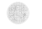
- FIG. 6 is a map of carrot defects on the surface of an epitaxial layer of the SiC epitaxial wafer of Comparative Example 1.
- FIG. 6 is a map of carrot defects on the surface of an epitaxial layer of a SiC epitaxial wafer of Comparative Example 2.
- 6 is a map of defects due to Si droplets on the surface of an epitaxial layer of the SiC epitaxial wafer of Comparative Example 2.
- FIG. 6 is a map of carrot defects on the surface of an epitaxial layer of the SiC epitaxial wafer of Example 2.
- FIG. 6 is a map of carrot defects on the surface of the epitaxial layer of the SiC epitaxial wafer of Example 3.
- FIG. 10 is a map of carrot defects on the surface of an epitaxial layer of a SiC epitaxial wafer of Comparative Example 3.
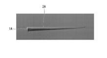
- FIG. 1 is an image of a carrot defect obtained by a confocal microscope (SICA6X, manufactured by Lasertec Corporation) which is a surface inspection apparatus using a confocal differential interference optical system.
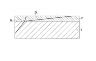
- FIG. 2 is a schematic cross-sectional view of the SiC epitaxial wafer near the carrot defect. 1 and 2, the left side is the step flow upstream side, and the right side is the step flow downstream side.
- ⁇ ⁇ Carrot defects are generated starting from threading dislocations and scratches on the substrate that existed in the SiC single crystal substrate. Scratches on the substrate can be eliminated by optimizing the processing conditions. Therefore, the threading dislocation existing in the SiC substrate is important as a cause of occurrence to be solved in order to reduce carrot defects.
- a prism area layer defect 2A is formed starting from the threading screw dislocation 1A in the SiC single crystal substrate. As a result, when viewed from the surface side of the epitaxial layer 2, it has a carrot shape.
- the carrot defect may be a device killer defect that causes an increase in leakage current.
- Si droplets defects caused by Si droplets
- the Si droplet is a foreign substance in which excessive Si atoms are condensed on the substrate surface during the epitaxial growth, and a Si droplet-induced defect is formed due to this.
- Si droplets are one form of foreign matter, and crystal growth is disturbed starting from this, and defects having the shape of small pits and bumps are generated on the epitaxial surface.
- the point that the starting point is a foreign object is different from the carrot defect whose starting point is a dislocation or the like.
- Si droplet defects can be distinguished from other defects by characteristics in size and form. Si droplet-induced defects are also disorder of crystallinity and crystal growth surface, and when they occur, they tend to occur at a stretch, which adversely affects device production.
- the method for manufacturing an SiC epitaxial wafer according to the present embodiment is a method for manufacturing an SiC epitaxial wafer having an epitaxial layer on an SiC single crystal substrate.
- the C / Si ratio in the first condition is 0.6 or less
- the Cl / Si ratio is 5.0 or more.
- a SiC epitaxial wafer is obtained by forming an epitaxial layer on a SiC single crystal substrate. Therefore, first, a SiC single crystal substrate is prepared.
- the manufacturing method of the SiC single crystal substrate is not particularly limited. For example, it is obtained by slicing a SiC ingot obtained by a sublimation method or the like.
- the obtained SiC single crystal substrate is subjected to chemical mechanical polishing (CMP) to remove damage caused by processing, and finished to a flat mirror surface.
- CMP chemical mechanical polishing
- a (0001) plane having an off angle is used as the plane orientation of the substrate.
- An off angle of 0.4 ° to 8 ° can be used, and a 4 ° off, that is, an off angle of 3.5 ° to 4.5 ° is preferably used.
- an epitaxial layer is epitaxially grown on the SiC single crystal substrate to produce a SiC epitaxial wafer.
- the epitaxial layer is obtained by step flow growth (atomic step to lateral growth) of SiC on the growth surface of the SiC single crystal substrate by, for example, a low pressure chemical vapor deposition (CVD) method.
- a raw material gas for SiC epitaxial growth silane or silane chloride is used as a silane-based gas, and a hydrocarbon such as ethylene or propane is used as a carbon-based gas. Further, nitrogen gas or the like is added as a dopant.
- an inert gas such as hydrogen or Ar is used.
- HCl may be added as a chlorine-based gas for the purpose of improving the growth rate.
- the ratio of Si and C on the surface during crystal growth has a great influence on impurity uptake, growth morphology, etc., so the C / Si ratio of the source gas is an important parameter to be controlled. .
- a parameter called Cl / Si ratio is also important.
- the C / Si ratio is a ratio of the C element and the Si element in the growth space, and is obtained from the silane-based gas and the carbon-based gas.
- the Cl / Si ratio is the ratio of the Cl element and the Si element in the growth space, and is determined from the chlorine gas or the total of the silane gas and the chlorine gas, and the silane gas.
- the Cl element in the silane gas also contributes to the Cl / Si ratio, so the Cl ratio in the Cl / Si ratio is The total amount of Cl element in the silane-based gas and Cl element in the Cl source gas is obtained.
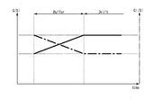
- FIG. 3 is a diagram schematically showing changes in the C / Si ratio and the Cl / Si ratio when an epitaxial layer is epitaxially grown on a SiC single crystal substrate.
- the graph shown by the solid line represents the change in the C / Si ratio
- the graph shown by the alternate long and short dash line represents the change in the Cl / Si ratio.
- Buffer corresponds to the growth condition when growing the buffer layer
- Shift corresponds to the growth condition when growing the drift layer
- the buffer layer is a layer that alleviates the difference in carrier concentration between the drift layer and the SiC single crystal substrate.
- the drift layer is a portion where an active layer is formed when a device is formed, and the thickness and carrier concentration are selected depending on the device to be manufactured. Since SiC is used in high voltage devices, the carrier concentration of the drift layer is as low as about 1 ⁇ 10 16 cm ⁇ 3 , for example. On the other hand, the SiC single crystal substrate has a high carrier concentration of about 1 ⁇ 10 18 cm ⁇ 3 or more. Therefore, it is common to provide a buffer layer having an intermediate carrier concentration.
- the thickness of the buffer layer is not particularly limited, but about 0.3 ⁇ m to 1 ⁇ m is often used in consideration of economy. Since the active layer of the device is formed in the drift layer, crystallinity and surface morphology are important, and the growth condition of the drift layer, for example, the C / Si ratio is determined with priority on the characteristics of the drift layer. On the other hand, the growth conditions of the buffer layer only have to have a constant carrier concentration without affecting the drift layer, and the degree of freedom in selecting the growth conditions is great.
- the SiC epitaxial wafer manufacturing method forms a part of the epitaxial layer under the first condition at the beginning of crystal growth when the epitaxial layer is crystal-grown. And forming a part of the SiC epitaxial layer under a second condition in which the Cl / Si ratio is decreased and the C / Si ratio is increased as compared with the first condition.
- ramping is performed to gradually decrease the C / Si ratio and gradually increase the Cl / Si ratio from the first condition to the second condition.
- ramping means that the growth conditions are gradually changed, and includes those that change the growth conditions stepwise and those that change the slope.
- the ramping process is preferably performed during the growth of the buffer layer so as not to affect the drift layer.
- the C / Si ratio and the Cl / Si ratio can be controlled by controlling the supply amount of silane-based gas, carbon-based gas, and chlorine-based gas.
- SiH 4 , SiHCl 3 , SiH 2 Cl 2 , SiH 3 Cl, SiCl 4, etc. can be used as the silane-based gas. Since SiHCl 3 , SiH 2 Cl 2 , SiH 3 Cl, and SiCl 4 contain a Cl element, they also function as a chlorine-based gas. In addition to this, HCl can also be used as the chlorine-based gas.
- alkanes such as propane can be used.
- the Cl / Si ratio can be controlled by controlling the C / Si ratio with SiH 2 Cl 2 gas and C 3 H 8 gas and changing the supply amount of HCl gas.
- the first condition for starting crystal growth is that the C / Si ratio is 0.6 or less and the Cl / Si ratio is 5.0 or more.
- the C / Si ratio in the first condition is preferably 0.4 to 0.6, and the Cl / Si ratio is preferably 5.0 to 8.0.
- the epitaxial layer preferably undergoes crystal growth while gradually changing the growth condition from the first condition to the second condition.
- the background carrier concentration means the carrier concentration of the epitaxial layer when no doping gas (for example, nitrogen or trimethylaluminum) is supplied.
- the carrier concentration is stably controlled, the background carrier concentration needs to be low.
- it is important to lower the background carrier concentration that is, a SiC epitaxial wafer having a high background carrier concentration cannot be suitably used for a SiC device. Therefore, by gradually increasing the C / Si ratio from the first condition in the ramping step, an increase in the background carrier concentration in the region (drift layer) used for the SiC device of the epitaxial layer can be suppressed.
- the growth rate of epitaxial growth cannot be increased.
- the gas containing Cl element etches SiC and contributes to cleaning of the growth surface.
- the Cl ratio in the growth atmosphere is too high, epitaxial growth proceeds and the growth surface is etched. As a result, the growth rate of the epitaxial layer becomes slow. The decrease in the growth rate leads to an increase in the manufacturing cost of the SiC epitaxial wafer.
- the C / Si ratio is gradually increased from the first condition. Therefore, the growth atmosphere approaches a condition in which Si droplets are hardly generated. That is, as the ramping process proceeds, it is not necessary to increase the Cl ratio in the growth atmosphere. Therefore, the growth rate can be increased while suppressing the generation of Si droplets by gradually decreasing the Cl / Si ratio in conjunction with the increase in the C / Si ratio in the ramping process.
- the growth conditions are gradually changed.
- the growth condition is suddenly changed from the first condition to the second condition, the growth atmosphere changes abruptly. Therefore, there is a portion where the Si concentration is high although the Cl concentration is locally low. It tends to occur.
- the ramping process it is possible to avoid the occurrence of portions where the Si concentration and the Cl concentration are locally increased or decreased, and the generation of Si droplets can be further suppressed.
- the growth condition is gradually switched from the first condition to the second condition to prevent the occurrence of overshoot, the C / Si ratio becomes excessively high, or the Cl / Si ratio is increased. It can suppress more becoming low too much.
- the rate of the C / Si ratio the possibility of carbon deposition can be reduced, and by suppressing the Cl / Si ratio from becoming excessively low, the cleanliness of the growth surface is reduced. In addition, it is possible to further suppress the generation of foreign matters and the like.
- the ramping process may be changed stepwise.
- the C / Si ratio in the second condition after changing the growth conditions is preferably 0.8 to 1.5, more preferably 0.9 to 1.2, and 0.95 to More preferably, 1.1.
- the second condition is within this range, the background carrier concentration in the drift layer can be reduced to such an extent that it is used for the SiC device. Further, the growth rate of the epitaxial layer is not significantly reduced.
- the time required for growing the buffer layer and the time for performing the ramping process are not necessarily matched.
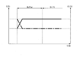
- FIG. 4 is a diagram schematically showing changes in the C / Si ratio and the Cl / Si ratio when the epitaxial layer is epitaxially grown on the SiC single crystal substrate.
- a graph indicated by a solid line represents a change in the C / Si ratio
- a graph indicated by a one-dot chain line represents a change in the Cl / Si ratio.
- Buffer corresponds to the growth condition when growing the buffer layer
- Shift corresponds to the growth condition when growing the drift layer.
- the time required for the ramping process may be 1/5 or more of the time required for forming the buffer layer. This may be 0.1 ⁇ m or more in terms of the thickness of the epitaxial layer. If the ramping process is performed within this range, the occurrence of carrot defects and Si droplets can be suppressed at the same time.
- the ramping process is preferably started simultaneously with the start of growth of the epitaxial layer.
- the carrot defect is caused by a small lattice disorder due to threading dislocations or surface damage, and is generated from the interface between the substrate and the epitaxial layer. That is, in order to suppress the occurrence of carrot defects, it is important immediately after the start of growth, and the influence of subsequent growth conditions is smaller. In the manufacturing method of the SiC epitaxial wafer according to the present embodiment, this is confirmed by ramping the growth conditions. For example, even when the period during which an epitaxial layer having a thickness of 0.1 ⁇ m is grown is changed by ramping, the effect of reducing carrot defects can be obtained effectively. This indicates that growth conditions at the very beginning of growth are important in the occurrence of carrot defects.
- the C / Si ratio can be lowered immediately after the start of the growth of the SiC epitaxial layer, the C / Si can be raised thereafter, and the Cl / Si ratio can be lowered in the latter half of the growth. While the C / Si ratio is low, Si droplets are likely to be generated, and this tendency is the same even during epitaxial growth. Therefore, Si droplets continue to be generated when the C / Si ratio remains low. Therefore, it is desirable to increase the C / Si ratio promptly except for the necessary growth period. As the C / Si ratio increases, the Cl / Si ratio can be lowered accordingly.
- the C / Si ratio immediately after the crystal growth can be lowered, and the Cl / Si can be lowered at an early stage, thereby increasing the growth rate of the epitaxial layer. be able to. If the ramping period can be shortened and ramping growth can be accommodated within the growth range of the buffer layer, the device layer conditions do not need to be changed, and the growth conditions of the device layer can be arbitrarily selected.
- Example 1 As the SiC single crystal substrate, a sliced SiC ingot produced by a sublimation method was used. The size of the SiC single crystal substrate was 3 inches. The surface of the SiC single crystal after slicing was subjected to rough polishing and precision polishing with diamond abrasive grains to flatten the growth surface for epitaxial growth. The polytype of the SiC single crystal substrate is 4H, and has an offset angle of 4 ° with respect to the ⁇ 11-20> direction with respect to the c-axis. Carrot defects are related to the threading dislocation density of the substrate. Therefore, in order to increase the accuracy of comparison of the effects, the examples and comparative examples use the same defect density obtained from the same ingot in each of the study of the 3-inch substrate and the study of the 4-inch substrate. It was.
- the SiC single crystal substrate was introduced into the growth furnace, and the epitaxial layer was grown to 10.5 ⁇ m while supplying dichlorosilane, propane, and HCl as the etching gas to the surface of the 4H—SiC single crystal substrate.
- the C / Si ratio was changed by changing the flow rates of dichlorosilane and propane, and the Cl / Si ratio was changed by adjusting the flow rate of HCl correspondingly.
- the epitaxial layer was a buffer layer having a high carrier concentration of 0.5 ⁇ m (thickness including a ramping process) and a drift layer having a low carrier concentration of 10 ⁇ m, and these were continuously grown. Nitrogen was used as the dopant.
- the growth conditions of the epitaxial layer were as follows. Growth pressure: 15 kPa Growth temperature: 1600 ° C Crystal growth conditions (C / Si ratio, Cl / Si ratio) First condition: C / Si ratio 0.6, Cl / Si ratio 5.0 Second condition: C / Si ratio 1.0, Cl / Si ratio 3.0 Epitaxial layer thickness formed in the ramping process: 0.5 ⁇ m Buffer layer thickness: 0.5 ⁇ m
- the foreign matter on the surface of the epitaxial layer of the obtained SiC epitaxial wafer was measured.
- the foreign matter was measured using Candela CS20 manufactured by KLA Tencor, and the size of the foreign matter was specified from the scattering cross section of the scattered light. It was confirmed in advance that there was a correlation between the size measured by candela evaluation using the scattering cross section and the type of foreign matter.
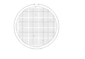
- FIG. 5 shows a map of carrot defects on the surface of the epitaxial layer of the SiC epitaxial wafer of Example 1.
- Comparative Example 1 a SiC epitaxial wafer was produced under the same conditions as Example 1 except that the epitaxial growth conditions were changed. In Comparative Example 1, the following conditions were used without changing the crystal growth conditions (C / Si ratio, Cl / Si ratio) on the way. Crystal growth conditions: C / Si ratio 1.0, Cl / Si ratio 3.0
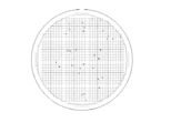
- FIG. 6 shows a map of carrot defects on the surface of the epitaxial layer of the SiC epitaxial wafer of Comparative Example 1.
- Comparative Example 2 a SiC epitaxial wafer was manufactured under the same conditions as in Example 1 except that the C / Si ratio and Cl / Si ratio conditions at the beginning of epitaxial growth were changed.
- the first condition of crystal growth conditions was as follows. Crystal growth conditions (C / Si ratio, Cl / Si ratio) First condition: C / Si ratio 0.60, Cl / Si ratio 3.0
- FIG. 7 shows a map of carrot defects on the surface of the epitaxial layer of the SiC epitaxial wafer of Comparative Example 2.
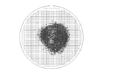
- FIG. 8 shows a map of Si droplet-induced defects on the surface of the epitaxial layer of the SiC epitaxial wafer.
- Example 2 ⁇ 4 inch substrate> (Example 2) In Example 2, the SiC single crystal substrate was changed to 4 inches. Other conditions were the same as in Example 1.
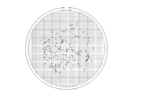
- FIG. 9 shows a map of carrot defects on the surface of the epitaxial layer of the SiC epitaxial wafer of Example 2.
- Example 3 The third embodiment is different from the second embodiment in that the time required for the ramping process is reduced to 1/5. Other conditions were the same as in Example 2. Crystal growth conditions (C / Si ratio, Cl / Si ratio) First condition: C / Si ratio 0.6, Cl / Si ratio 5.0 Second condition: C / Si ratio 1.0, Cl / Si ratio 3.0 Epitaxial layer thickness deposited in the ramping process: 0.1 ⁇ m Buffer layer thickness: 0.5 ⁇ m
- FIG. 10 shows a map of carrot defects on the surface of the epitaxial layer of the SiC epitaxial wafer of Example 3.
- Comparative Example 3 an SiC epitaxial wafer was produced under the same conditions as in Example 2 except that the crystal growth conditions were changed.
- the crystal growth conditions (C / Si ratio, Cl / Si ratio) were set as follows without changing the conditions on the way. Crystal growth conditions: C / Si ratio 1.0, Cl / Si ratio 3.0 That is, Comparative Example 3 is different from Comparative Example 1 in that the size of the SiC single crystal substrate is changed.
- FIG. 11 shows a map of carrot defects on the surface of the epitaxial layer of the SiC epitaxial wafer of Comparative Example 3.
Landscapes
- Chemical & Material Sciences (AREA)
- Metallurgy (AREA)
- Engineering & Computer Science (AREA)
- Materials Engineering (AREA)
- Organic Chemistry (AREA)
- General Chemical & Material Sciences (AREA)
- Chemical Kinetics & Catalysis (AREA)
- Crystallography & Structural Chemistry (AREA)
- Inorganic Chemistry (AREA)
- Mechanical Engineering (AREA)
- Crystals, And After-Treatments Of Crystals (AREA)
- Chemical Vapour Deposition (AREA)
- Recrystallisation Techniques (AREA)
Abstract
このSiCエピタキシャルウェハの製造方法は、SiC単結晶基板上にエピタキシャル層を有するSiCエピタキシャルウェハの製造方法であって、前記エピタキシャル層を結晶成長する際に、結晶成長を開始する初期に第1の条件でエピタキシャル層の一部を形成する工程と、前記第1の条件よりもCl/Si比を減少させ、かつ、C/Si比を増加させた第2の条件でSiCエピタキシャル層の一部を形成する工程と、を有し、前記第1の条件におけるC/Si比は0.6以下であり、Cl/Si比は5.0以上である。
Description
本発明は、SiCエピタキシャルウェハの製造方法に関する。本願は、2015年12月24日に、日本に出願された特願2015-250942に基づき優先権を主張し、その内容をここに援用する。
炭化珪素(SiC)は、多くの優れた特性を有する。例えば、シリコン(Si)に比べて絶縁破壊電界は1桁大きく、バンドギャップは3倍大きく、さらに、熱伝導率が3倍程度高い。炭化珪素(SiC)は、パワーデバイス、高周波デバイス、高温動作デバイス等への応用が期待されている。
SiCデバイスの実用化の促進には、高品質のSiCエピタキシャルウェハ及び高品質のエピタキシャル成長技術の確立が不可欠である。
SiCデバイスは、SiCエピタキシャルウェハを用いて作製される。SiCエピタキシャルウェハは、昇華再結晶法等で成長させたSiCのバルク単結晶から加工して得られたSiC単結晶基板上に、化学的気相成長法(Chemical Vapor Deposition:CVD)等によってデバイスの活性領域となるエピタキシャル層(膜)を成長させて得られる。
例えば、(0001)面から<11-20>方向にオフ角を有する面を成長面とするSiC単結晶基板上に、SiCをステップフロー成長(原子ステップからの横方向成長)させて、4Hのエピタキシャル層を成長させる。
SiCエピタキシャルウェハに含まれる欠陥には、エピタキシャル層表面に表出した特徴的な形状をもつキャロット欠陥(キャロット型欠陥、ニンジン状欠陥)と呼ばれる欠陥がある。キャロット欠陥は、エピタキシャル層表面に現れる欠陥として、三角欠陥、コメット欠陥等と並んで代表的なものである。キャロット欠陥は、数が多くまた形状的にも数十μmと大きいため、結晶の完全性を求める半導体デバイス用エピウェハ製造において、低減することが望まれている(特許文献1~3)。
キャロット欠陥の構造は、基底面積層欠陥とプリズム型積層欠陥によって構成されることが解明されおり、SiCエピタキシャル成長の分野では識別可能な欠陥として定義されている。キャロット欠陥は、基板内の貫通転位等がエピ成長時に転換することで生成すると考えられている。
キャロット欠陥密度を低減させる方法として、いくつかの方法が提案されている。特許文献1には、第1のエピタキシャル層を成長した後、成長を停止して表面のエッチングを行った後、第2のエピタキシャル層を成長させる方法が記載されている。特許文献2には、低いC/Si比をもつ原料ガス組成の抑止層を設ける方法が記載されている。特許文献3には、CMP加工で特定のらせん転位によるピットを一定形状にした基板を用いる方法が記載されている。
しかし、C/Si比を低くしすぎると、エピタキシャル成長中にSiドロップレットが発生しやすくなるという問題がある。Siドロップレットは、過剰なSi原子が基板表面に凝縮したもので、それに起因する結晶欠陥を発生させる。
例えば、特許文献2のC/Si比が低い条件でSiCエピタキシャル層を実際に成長させると、キャロット欠陥の抑制とドロプレットの発生の抑制とを両立させることができなかった。つまり、安定的にキャロット欠陥の少ないエピタキシャルウェハを得る方法は知られていない。
例えば、特許文献2のC/Si比が低い条件でSiCエピタキシャル層を実際に成長させると、キャロット欠陥の抑制とドロプレットの発生の抑制とを両立させることができなかった。つまり、安定的にキャロット欠陥の少ないエピタキシャルウェハを得る方法は知られていない。
上述の通り、キャロット欠陥を減少させようとしてC/Si比を低下させると、Siドロップレットが発生しやすくなってしまう。そのため、キャロット欠陥及びSiドロップレットの発生を共に抑制できるSiCエピタキシャルウェハの製造方法が求められている。
本発明は上記問題に鑑みてなされたものであり、キャロット欠陥及びSiドロップレットの発生を同時に抑制できるSiCエピタキシャルウェハの製造方法を得ることを目的とする。
本発明者らは、鋭意検討の結果、結晶成長初期におけるC/Si比を小さくかつCl/Siを高くし、それぞれの成長条件を成長過程で徐々に変化させることで、キャロット欠陥及びSiドロップレットの発生を同時に抑制できることを見出し、発明を完成させた。
すなわち、本発明は、上記課題を解決するため、以下の手段を提供する。
すなわち、本発明は、上記課題を解決するため、以下の手段を提供する。
(1)本発明の一態様に係るSiCエピタキシャルウェハの製造方法は、SiC単結晶基板上にエピタキシャル層を有するSiCエピタキシャルウェハの製造方法であって、前記エピタキシャル層を結晶成長する際に、結晶成長を開始する初期に第1の条件でエピタキシャル層の一部を形成する工程と、前記第1の条件よりもCl/Si比を減少させ、かつ、C/Si比を増加させた第2の条件でSiCエピタキシャル層の一部を形成する工程と、を有し、前記第1の条件におけるC/Si比は0.6以下であり、Cl/Si比は5.0以上である。
(2)上記(1)に記載のSiCエピタキシャルウェハの製造方法における前記第1の条件において、Cl元素の供給源として塩化シラン(SiH4-nCln:n=0~4)と塩化水素(HCl)とを共に用いてもよい。
(3)上記(1)又は(2)のいずれかに記載のSiCエピタキシャルウェハの製造方法において、前記第2の条件におけるC/Si比は0.8~1.5であり、Cl/Si比は0~4であってもよい。
(4)上記(1)~(3)のいずれか一つに記載のSiCエピタキシャルウェハの製造方法において、前記エピタキシャル層を結晶成長する際に、前記第1の条件から前記第2の条件に向かって、C/Si比を徐々に減少させると共にCl/Si比を徐々に増加させるランピング工程を行ってもよい。
(5)上記(4)に記載のSiCエピタキシャルウェハの製造方法において、前記エピタキシャル層が、前記SiC単結晶基板側から順にバッファ層とドリフト層とを有し、前記バッファ層を成長させる際に前記ランピング工程を行ってもよい。
(6)上記(5)に記載のSiCエピタキシャルウェハの製造方法において、前記ランピング工程に要する時間が、前記バッファ層を成膜するのに要する時間の1/5以上であってもよい。
(7)上記(5)又は(6)のいずれかに記載のエピタキシャルウェハの製造方法において、前記ランピング工程で結晶成長するエピタキシャル層の層厚が、0.1μm以上であってもよい。
(8)上記(5)~(7)のいずれか一つに記載のエピタキシャルウェハの製造方法において、前記ランピング工程が、前記エピタキシャル層の成長開始と同時に開始されてもよい。
本発明の一態様に係るSiCエピタキシャルウェハの製造方法によれば、キャロット欠陥及びSiドロップレットの発生を同時に抑制することができる。
以下、本実施形態にかかるSiCエピタキシャルウェハの製造方法について、図を適宜参照しながら詳細に説明する。以下の説明で用いる図面は、本発明の特徴をわかりやすくするために便宜上特徴となる部分を拡大して示している場合があり、各構成要素の寸法比率などは実際とは異なっていることがある。以下の説明において例示される材質、寸法等は一例であって、本発明はそれらに限定されるものではなく、その要旨を変更しない範囲で適宜変更して実施することが可能である。
(キャロット欠陥)
図1は、共焦点微分干渉光学系を用いた表面検査装置である共焦点顕微鏡(レーザーテック株式会社製、SICA6X)によって得られたキャロット欠陥の像である。また図2は、キャロット欠陥近傍のSiCエピタキシャルウェハの断面模式図である。図1及び図2において、図示左側がステップフロー上流側であり、図示右側がステップフロー下流側である。
図1は、共焦点微分干渉光学系を用いた表面検査装置である共焦点顕微鏡(レーザーテック株式会社製、SICA6X)によって得られたキャロット欠陥の像である。また図2は、キャロット欠陥近傍のSiCエピタキシャルウェハの断面模式図である。図1及び図2において、図示左側がステップフロー上流側であり、図示右側がステップフロー下流側である。
キャロット欠陥は、SiC単結晶基板に存在した貫通転位や基板上の傷を起点に発生する。基板上の傷は加工条件の最適化で無くすことができる。そのため、SiC基板に存在する貫通転位は、キャロット欠陥を低減するために解決すべき発生起因として重要である。図2におけるキャロット欠陥は、SiC単結晶基板内の貫通螺旋転位1Aを起点としてプリズム面積層欠陥2Aが形成されている。その結果、エピタキシャル層2の表面側から見て、キャロット状となっている。キャロット欠陥は、SiCデバイス内に組み込まれると、リーク電流の増大等の原因となるデバイスキラー欠陥となる場合がある。
(Siドロップレット、Siドロプレット起因欠陥)
Siドロップレットとは、エピタキシャル成長中に過剰なSi原子が基板表面に凝縮した異物であり、これを起因としてSiドロプレット起因欠陥が形成される。Siドロップレットは異物の一態様であり、それを起点として結晶成長の乱れが生じ、エピタキシャル表面で小型のピットやバンプの形状を持つ欠陥が発生する。起点が異物である点が、起点が転位等であるキャロット欠陥とは異なる。実際にエピタキシャル成長させる場合は極端にSi過剰な条件はとらないため、Siドロプレットは小型であり、Siドロプレット起因欠陥も小型のものとなる。Siドロプレット欠陥は、大きさや形態上の特徴で、他欠陥と識別することができる。Siドロプレット起因欠陥も、結晶性や結晶成長表面の乱れであり、また発生する場合は一気に多数発生する傾向があるため、デバイス制作に悪影響を与える。
Siドロップレットとは、エピタキシャル成長中に過剰なSi原子が基板表面に凝縮した異物であり、これを起因としてSiドロプレット起因欠陥が形成される。Siドロップレットは異物の一態様であり、それを起点として結晶成長の乱れが生じ、エピタキシャル表面で小型のピットやバンプの形状を持つ欠陥が発生する。起点が異物である点が、起点が転位等であるキャロット欠陥とは異なる。実際にエピタキシャル成長させる場合は極端にSi過剰な条件はとらないため、Siドロプレットは小型であり、Siドロプレット起因欠陥も小型のものとなる。Siドロプレット欠陥は、大きさや形態上の特徴で、他欠陥と識別することができる。Siドロプレット起因欠陥も、結晶性や結晶成長表面の乱れであり、また発生する場合は一気に多数発生する傾向があるため、デバイス制作に悪影響を与える。
このように、キャロット欠陥及びSiドロップレットはSiCデバイスの不良を生み出す原因であり、低減が求められる。
(SiCエピタキシャル層の製造方法)
本実施形態に係るSiCエピタキシャルウェハの製造方法は、SiC単結晶基板上にエピタキシャル層を有するSiCエピタキシャルウェハの製造方法であって、エピタキシャル層を結晶成長する際に、結晶成長を開始する初期に第1の条件でエピタキシャル層の一部を形成する工程と、第1の条件よりもCl/Si比を減少させ、かつ、C/Si比を増加させた第2の条件でSiCエピタキシャル層の一部を形成する工程と、を有する。この際、第1の条件におけるC/Si比は0.6以下であり、Cl/Si比は5.0以上である。
本実施形態に係るSiCエピタキシャルウェハの製造方法は、SiC単結晶基板上にエピタキシャル層を有するSiCエピタキシャルウェハの製造方法であって、エピタキシャル層を結晶成長する際に、結晶成長を開始する初期に第1の条件でエピタキシャル層の一部を形成する工程と、第1の条件よりもCl/Si比を減少させ、かつ、C/Si比を増加させた第2の条件でSiCエピタキシャル層の一部を形成する工程と、を有する。この際、第1の条件におけるC/Si比は0.6以下であり、Cl/Si比は5.0以上である。
以下、具体的に本発明の一態様に係るSiCエピタキシャルウェハの製造方法について説明する。
SiCエピタキシャルウェハは、SiC単結晶基板上にエピタキシャル層を形成して得られる。そのため、まずSiC単結晶基板を準備する。
SiCエピタキシャルウェハは、SiC単結晶基板上にエピタキシャル層を形成して得られる。そのため、まずSiC単結晶基板を準備する。
SiC単結晶基板の作製方法は特に問わない。例えば、昇華法等で得られたSiCインゴットをスライスして得られる。
得られたSiC単結晶基板は、表面を化学的機械研磨(CMP)することにより加工により発生したダメージを除去し、平坦な鏡面に仕上げられる。
基板の面方位としては、(0001)面で、オフ角度が設けられたものを使用する。オフ角度は0.4°~8°の物が用いることができ、4°オフすなわちオフ角度が3.5°~4.5°のものが好適に用いられる。
基板の面方位としては、(0001)面で、オフ角度が設けられたものを使用する。オフ角度は0.4°~8°の物が用いることができ、4°オフすなわちオフ角度が3.5°~4.5°のものが好適に用いられる。
次いで、SiC単結晶基板上にエピタキシャル層をエピタキシャル成長させ、SiCエピタキシャルウェハを作製する。
エピタキシャル層は、例えば減圧の化学気相成長(CVD)法等によりSiC単結晶基板の成長面上に、SiCがステップフロー成長(原子ステップから横方向成長)して得られる。
SiCエピタキシャル成長の原料ガスとしては、シラン系ガスとしてシランや塩化シランが用いられ、炭素系ガスとしてエチレンやプロパンなどの炭化水素が用いられる。さらにドーパントとし窒素ガスなどが添加される。これらの原料ガスを運ぶキャリアガスとしては、水素やArなどの不活性ガスが用いられる。この他、成長速度の改善等の目的で塩素系ガスとしてHClを添加してもよい。
エピタキシャル層は、例えば減圧の化学気相成長(CVD)法等によりSiC単結晶基板の成長面上に、SiCがステップフロー成長(原子ステップから横方向成長)して得られる。
SiCエピタキシャル成長の原料ガスとしては、シラン系ガスとしてシランや塩化シランが用いられ、炭素系ガスとしてエチレンやプロパンなどの炭化水素が用いられる。さらにドーパントとし窒素ガスなどが添加される。これらの原料ガスを運ぶキャリアガスとしては、水素やArなどの不活性ガスが用いられる。この他、成長速度の改善等の目的で塩素系ガスとしてHClを添加してもよい。
SiCの成長では、結晶成長時の表面のSiとCの比が不純物の取り込みや成長モフォロジー等に大きな影響を与えるため、原料ガスのC/Si比が、制御すべき重要なパラメーターとなっている。また、結晶成長表面近傍のClの存在が、結晶成長に影響を与えるためCl/Si比というパラメーターも重要である。
C/Si比は、成長空間中におけるC元素とSi元素の比であり、シラン系ガスと炭素系ガスから求められる。Cl/Si比は、成長空間中におけるCl元素とSi元素の比であり、塩素系ガスまたはシラン系ガスと塩素系ガスの合計と、シラン系ガスと、から求められる。シラン系ガスとして塩化シラン(SiH4-nCln:n=0~4)を用いる場合は、シラン系ガス中のCl元素もCl/Si比に寄与するため、Cl/Si比におけるCl比は、シラン系ガス中のCl元素とCl原料ガス中のCl元素の合計から求める。
C/Si比は、成長空間中におけるC元素とSi元素の比であり、シラン系ガスと炭素系ガスから求められる。Cl/Si比は、成長空間中におけるCl元素とSi元素の比であり、塩素系ガスまたはシラン系ガスと塩素系ガスの合計と、シラン系ガスと、から求められる。シラン系ガスとして塩化シラン(SiH4-nCln:n=0~4)を用いる場合は、シラン系ガス中のCl元素もCl/Si比に寄与するため、Cl/Si比におけるCl比は、シラン系ガス中のCl元素とCl原料ガス中のCl元素の合計から求める。
図3は、SiC単結晶基板上にエピタキシャル層をエピタキシャル成長させる際のC/Si比及びCl/Si比の変化を模式的に示した図である。図3において、実線で示したグラフがC/Si比の変化を表しており、一点鎖線で示したグラフがCl/Si比の変化を表している。
また図3において、Bufferはバッファ層を成長する際の成長条件に対応し、Driftはドリフト層を成長する際の成長条件に対応する。ここでバッファ層は、ドリフト層とSiC単結晶基板のキャリア濃度の違いを緩和する層である。ドリフト層はデバイスを形成する際に能動層が形成される部分で、作製されるデバイスによってそれぞれ厚さやキャリア濃度が選択される。SiCは高耐圧デバイスに用いられるため、ドリフト層のキャリア濃度は、たとえば1×1016cm-3程度と低い。一方、SiC単結晶基板はキャリア濃度が高く1×1018cm-3程度以上である。そのため、その中間的なキャリア濃度のバッファ層を設けることが一般的である。バッファ層の厚さは特に限定されるものではないが、経済性も考慮して0.3μm~1μm程度が用いられることが多い。
ドリフト層はデバイスの能動層が形成されるため、結晶性や表面モフォロジーが重要であり、ドリフト層の成長条件、たとえばC/Si比は、ドリフト層の特性を優先して決定される。一方、バッファ層の成長条件は、ドリフト層に影響を与えずに一定のキャリア濃度になればよく、成長条件の選定の自由度は大きい。
ドリフト層はデバイスの能動層が形成されるため、結晶性や表面モフォロジーが重要であり、ドリフト層の成長条件、たとえばC/Si比は、ドリフト層の特性を優先して決定される。一方、バッファ層の成長条件は、ドリフト層に影響を与えずに一定のキャリア濃度になればよく、成長条件の選定の自由度は大きい。
図3に示すように、本実施形態に係るSiCエピタキシャルウェハの製造方法は、エピタキシャル層を結晶成長する際に、結晶成長を開始する初期に第1の条件でエピタキシャル層の一部を形成する工程と、第1の条件よりもCl/Si比を減少させ、かつ、C/Si比を増加させた第2の条件でSiCエピタキシャル層の一部を形成する工程と、を有する。また第1の条件から第2の条件に向かって、C/Si比を徐々に減少すると共にCl/Si比を徐々に増加するランピングを行っている。ここでランピングは、成長条件を徐々に変化させることを意味し、成長条件を階段状に変化させるものも、スロープ状に変化させるものも含む。ランピング工程は、ドリフト層に影響を与えない様に、バッファ層の成長中に行われることが好ましい。
C/Si比及びCl/Si比の制御は、シラン系ガス、炭素系ガス、塩素系ガスの供給量を制御することで行うことができる。シラン系ガスとしては、SiH4、SiHCl3、SiH2Cl2、SiH3Cl、SiCl4等を用いることができる。SiHCl3、SiH2Cl2、SiH3Cl、SiCl4は、Cl元素を含むため、塩素系ガスとしても機能する。塩素系ガスとしては、この他にHClも用いることができる。また炭素系ガスとしては、プロパン等のアルカンを用いることができる。
例えば、SiH2Cl2ガスとC3H8ガスでC/Si比を制御し、HClガスの供給量を変化することで、Cl/Si比を制御することができる。
例えば、SiH2Cl2ガスとC3H8ガスでC/Si比を制御し、HClガスの供給量を変化することで、Cl/Si比を制御することができる。
ランピング工程において、結晶成長を開始する際の第1の条件は、C/Si比が0.6以下であり、Cl/Si比が5.0以上である。また第1の条件のC/Si比は0.4~0.6であることが好ましく、Cl/Si比は5.0~8.0であることが好ましい。
C/Si比及びCl/Si比のいずれか一方の条件を制御したのみでは、キャロット欠陥及びSiドロップレットのいずれも同時に抑制することができない。
例えば、C/Si比を0.6以下としCl/Si比を制御しない場合、キャロット欠陥の発生は抑制することができる。しかしながら、成長雰囲気中のSiの比率が高くなり、Siドロップレットが発生してしまう。
一方で、Cl/Si比を5.0以上としC/Si比を制御しない場合、キャロット欠陥が発生してしまう。
例えば、C/Si比を0.6以下としCl/Si比を制御しない場合、キャロット欠陥の発生は抑制することができる。しかしながら、成長雰囲気中のSiの比率が高くなり、Siドロップレットが発生してしまう。
一方で、Cl/Si比を5.0以上としC/Si比を制御しない場合、キャロット欠陥が発生してしまう。
これに対し、第1の条件のC/Si比及びCl/Si比をこの範囲内にすることで、キャロット欠陥とSiドロップレットの発生を同時に抑制することができる。結晶成長を開始する際のC/Si比を0.6以下とすることで、キャロット欠陥の発生が抑制される。
さらに、成長雰囲気中のCl比率を高めることで、成長面においてSiClxが形成され、Si同士が凝集、核成長することを抑制できる。すなわち、Siドロップレットの発生を抑制することができる。
さらに、成長雰囲気中のCl比率を高めることで、成長面においてSiClxが形成され、Si同士が凝集、核成長することを抑制できる。すなわち、Siドロップレットの発生を抑制することができる。
エピタキシャル層は、成長条件を第1の条件から第2の条件に徐々に変化させながら結晶成長を行うことが好ましい。
C/Si比を第1の条件のまま結晶成長を進めると、得られるエピタキシャル層のバックグラウンドキャリア濃度が高くなる。バックグラウンドキャリア濃度とは、ドーピングガス(例えば、窒素やトリメチルアルミニウム)を供給しないときのエピタキシャル層のキャリア濃度を意味する。安定的にキャリア濃度を制御する場合、バックグラウンドキャリア濃度が低い必要がある。特に低いキャリア濃度の制御を行う場合には、バックグラウンドキャリア濃度を低くすることが重要である。すなわち、バックグラウンドキャリア濃度が高いSiCエピタキシャルウェハは、SiCデバイスに好適に利用することができない。そのためランピング工程において、第1の条件からC/Si比を徐々に増加させることで、エピタキシャル層のSiCデバイスに用いられる領域(ドリフト層)におけるバックグラウンドキャリア濃度の増加を抑えることができる。
一方でCl/Si比を第1の条件のまま結晶成長を進めると、エピタキシャル成長の成長速度を高めることができない。Cl元素を含むガスは、SiCをエッチングし、成長面の清浄化に寄与する。しかしながら、成長雰囲気中のCl比が高すぎると、エピタキシャル成長が進むと共に、成長表面がエッチングされる。その結果、エピタキシャル層の成長速度が遅くなる。成長速度の低下は、SiCエピタキシャルウェハの製造コストの増加に繋がる。
C/Si比は第1の条件から徐々に増加させる。そのため、成長雰囲気は、Siドロップレットが発生し難い条件に近づいていく。すなわち、ランピング工程が進むにつれて、成長雰囲気におけるCl比を高める必要が無くなる。そこで、ランピング工程でC/Si比の増加に連動させて、Cl/Si比を徐々に減少させていくことで、Siドロップレットの発生を抑制しつつ、成長速度を高めることができる。
またランピング工程では、徐々に成長条件を変化させる。実際の装置において成長条件を第1の条件から第2の条件に急激に変化させると、成長雰囲気が急激に変化するため、局所的にCl濃度が低いにも関わらずSi濃度が高い部分等が生じやすくなる。ランピング工程を行うことで、局所的にSi濃度及びCl濃度が濃くなる又は薄くなる部分の発生を避けることができ、Siドロップレットの発生をより抑制することができる。
また現実の装置の制御において、成長条件を第1の条件から第2の条件に徐々に切り替えることで、オーバーシュートの発生を防ぎ、C/Si比が過剰に高くなったり、Cl/Si比が過剰に低くなることをより抑制することができる。C/Si比が過剰に高まることを抑制することで、炭素析出の可能性を低減することができ、Cl/Si比が過剰に低くなることを抑制することで、成長面の清浄性が低下し、異物等が発生することをより抑制することができる。オーバーシュートが生じないようにした場合、ランピング工程を階段状に変化させてもよい。
成長条件を変化させた後の第2の条件におけるC/Si比は、0.8~1.5であることが好ましく、0.9~1.2であることがより好ましく、0.95~1.1であることがさらに好ましい。また、Cl/Si比は、0~4であることが好ましく、1~3であることがより好ましく、2~3であることがさらに好ましい。すなわち、十分に時間をかけて変化させれば、最終的にSi原料としてシランを用い、HClを使用しないCl/Si=0とすることもできる。また、HClを用いずにSiHCl3を用いればCl/Si=3であり、SiH2Cl2を用いればCl/Si=2となり、単一の原料でSiとClを供給できる。すなわち、Cl元素とSi元素を安定的に供給できる。
第2の条件がこの範囲内であれば、ドリフト層におけるバックグラウンドキャリア濃度をSiCデバイスに用いる程度に低減することができる。またエピタキシャル層の成長速度が著しく低下することもない。
また第1の条件を含むエピタキシャル層を成長する際には、Si原料として、塩化シランを用いることが望ましい。単一の原料にSiとClを含むため、基板表面でのCl/Siを安定的に維持することができ、また腐食性が強く取り扱いにくいHClの使用を減らすことができる。
また第1の条件において、Cl/Si比は5以上である。Si原料として塩化シランの中で最もCl/Si比が高いSiHCl3を用いた場合でも、Cl/Si=3であり、さらにHClを加える必要がある。SiCのCVD原料としてSiCl4を用いることもできるが、この場合でもCl/Si=4である。すなわち、第1の条件において塩素を含むSi原料を用いた場合、HClを合わせて使用することで、所定のCl/Si比が実現される。
また第1の条件において、Cl/Si比は5以上である。Si原料として塩化シランの中で最もCl/Si比が高いSiHCl3を用いた場合でも、Cl/Si=3であり、さらにHClを加える必要がある。SiCのCVD原料としてSiCl4を用いることもできるが、この場合でもCl/Si=4である。すなわち、第1の条件において塩素を含むSi原料を用いた場合、HClを合わせて使用することで、所定のCl/Si比が実現される。
またバッファ層を成長するのに要する時間と、ランピング工程を行う時間は必ずしも一致させる必要はない。
図4は、SiC単結晶基板上にエピタキシャル層をエピタキシャル成長させる際のC/Si比及びCl/Si比の変化を模式的に示した図である。図4において、実線で示したグラフがC/Si比の変化を表しており、一点鎖線で示したグラフがCl/Si比の変化を表している。Bufferはバッファ層を成長する際の成長条件に対応し、Driftはドリフト層を成長する際の成長条件に対応する。
図4に示すように、ランピング工程に要する時間は、バッファ層を成膜するのに要する時間の1/5以上であればよい。これは、エピタキシャル層の層厚に換算すると、0.1μm以上であればよい。この範囲でランピング工程を行えば、キャロット欠陥とSiドロップレットの発生を同時に抑制することができる。
またランピング工程は、エピタキシャル層の成長開始と同時に開始されることが好ましい。キャロット欠陥は、貫通転位や表面のダメージによる微小な格子乱れが原因となり、基板とエピタキシャル層の界面を起点として発生する。すなわち、キャロット欠陥の発生を抑制するためには、成長開始直後が重要であり、その後の成長条件の影響はより小さい。本実施形態に係るSiCエピタキシャルウェハの製造方法では、成長条件をランピングさせることでそのことを確認した。例えば、0.1μmの厚さ分のエピタキシャル層を成長させる期間をランピングにより変化させた場合でも、有効にキャロット欠陥の低減効果が得られた。これは、成長のごく初期の成長条件が、キャロット欠陥の発生において重要であることを示している。そのため、SiCエピタキシャル層の成長開始直後においてC/Si比を低くし、その後はC/Siを高くすることができ、成長後半においてCl/Si比を低くすることができる。C/Si比が低い間はSiドロプレットが発生する可能性が高く、この傾向はエピタキシャル成長中でも同様である。そのため、C/Si比が低いままの場合、Siドロプレットが発生し続ける。したがって、必要な成長期間を除いてはC/Si比は速やかにあげることが望ましい。C/Si比が高くなれば、Cl/Si比もそれに応じて下げることができる。すなわち、エピタキシャル層の成長開始と同時にランピング工程を行うことで、結晶成長直後のC/Si比を低くしつつ、Cl/Siを早い段階で低くし始めることができ、エピタキシャル層の成長速度を高めることができる。
また、ランピング期間を短くし、バッファ層の成長範囲内でランピング成長を収めることができれば、デバイス層の条件を変更しなくてもよく、デバイス層の成長条件を任意に選ぶことができる。
また、ランピング期間を短くし、バッファ層の成長範囲内でランピング成長を収めることができれば、デバイス層の条件を変更しなくてもよく、デバイス層の成長条件を任意に選ぶことができる。
上述のように、本発明の一態様に係るSiCエピタキシャルウェハの製造方法によれば、キャロット欠陥及びSiドロップレットの発生を共に抑制することができる。
以下、本発明の実施例について説明する。なお、本発明は以下の実施例のみに限定されるものではない。
<3インチ基板>
(実施例1)
SiC単結晶基板は昇華法で作製されたSiCインゴットをスライスしたものを使用した。SiC単結晶基板のサイズは3インチとした。スライス後のSiC単結晶の表面は、粗研磨とダイアモンド砥粒による精密研磨を行い、エピタキシャル成長を行うための成長面を平坦化した。SiC単結晶基板のポリタイプは4Hであり、c軸に対して<11-20>方向に対して4°のオフセット角を有する。
キャロット欠陥は、基板の貫通転位密度と関係する。その為、効果の比較の精度を高めるために、実施例と比較例は、3インチ基板の検討と4インチ基板の検討のそれぞれにおいて、同じインゴットから得られた欠陥密度が同じレベルの物を用いた。
(実施例1)
SiC単結晶基板は昇華法で作製されたSiCインゴットをスライスしたものを使用した。SiC単結晶基板のサイズは3インチとした。スライス後のSiC単結晶の表面は、粗研磨とダイアモンド砥粒による精密研磨を行い、エピタキシャル成長を行うための成長面を平坦化した。SiC単結晶基板のポリタイプは4Hであり、c軸に対して<11-20>方向に対して4°のオフセット角を有する。
キャロット欠陥は、基板の貫通転位密度と関係する。その為、効果の比較の精度を高めるために、実施例と比較例は、3インチ基板の検討と4インチ基板の検討のそれぞれにおいて、同じインゴットから得られた欠陥密度が同じレベルの物を用いた。
次いで、SiC単結晶基板を成長炉内に導入し、4H-SiC単結晶基板の表面に対して、原料ガスとしてジクロロシラン、プロパン、エッチングガスとしてHClを供給しながら、エピタキシャル層を10.5μm成長させた。ジクロロシランとプロパンの流量を変えることによりC/Si比を変化させ、それに対応してHClの流量を調整することでCl/Si比を変化させた。エピタキシャル層は、キャリア濃度の高いバッファ層0.5μm(ランピング工程を含む厚さ)とキャリア濃度の低いドリフト層10μmとし、これらを連続して成長した。ドーパントは窒素を用いた。
エピタキシャル層の成長条件は以下とした。
成長圧力:15kPa
成長温度:1600℃
結晶成長条件(C/Si比、Cl/Si比)
第1条件:C/Si比 0.6、Cl/Si比 5.0
第2条件:C/Si比 1.0、Cl/Si比 3.0
ランピング工程で成膜したエピタキシャル層の層厚:0.5μm
バッファ層の層厚:0.5μm
成長圧力:15kPa
成長温度:1600℃
結晶成長条件(C/Si比、Cl/Si比)
第1条件:C/Si比 0.6、Cl/Si比 5.0
第2条件:C/Si比 1.0、Cl/Si比 3.0
ランピング工程で成膜したエピタキシャル層の層厚:0.5μm
バッファ層の層厚:0.5μm
得られたSiCエピタキシャルウェハのエピタキシャル層表面の異物を測定した。異物は、KLAテンコール社製のCandela CS20を用いて測定し、散乱光の散乱断面積から異物のサイズを特定した。散乱断面積を用いたカンデラ評価で測定したサイズと異物種に相関があることは事前に確認した。
その結果、キャロット欠陥は10個であり、Siドロップレットはほとんど見当たらなかった。Siドロップレットが発生した場合は、多数発生するため、数は数えなかった。またSiドロップレットは、エピタキシャル層表面では、Siドロップレット起因欠陥として観察される。以下、Siドロップレットそのもの及びSiドロップレット起因欠陥を含めて、Siドロップレットと表す。図5に、実施例1のSiCエピタキシャルウェハのエピタキシャル層表面のキャロット欠陥のマップを示す。
(比較例1)
比較例1では、実施例1とエピタキシャル成長条件を変更した点以外、同様の条件でSiCエピタキシャルウェハを作製した。
比較例1では、結晶成長条件(C/Si比、Cl/Si比)を途中で変更することなく以下の条件とした。
結晶成長条件:C/Si比 1.0、Cl/Si比 3.0
比較例1では、実施例1とエピタキシャル成長条件を変更した点以外、同様の条件でSiCエピタキシャルウェハを作製した。
比較例1では、結晶成長条件(C/Si比、Cl/Si比)を途中で変更することなく以下の条件とした。
結晶成長条件:C/Si比 1.0、Cl/Si比 3.0
得られたSiCエピタキシャルウェハの表面を実施例1と同様の手段で測定した。その結果、キャロット欠陥は31個であり、Siドロップレットはほとんど見当たらなかった。図6に、比較例1のSiCエピタキシャルウェハのエピタキシャル層表面のキャロット欠陥のマップを示す。
(比較例2)
比較例2では、実施例1とエピタキシャル成長開始初期のC/Si比とCl/Si比条件を変更した点以外、同様の条件でSiCエピタキシャルウェハを作製した。
比較例2では、結晶成長条件の第1条件を以下の条件とした。
結晶成長条件(C/Si比、Cl/Si比)
第1条件:C/Si比 0.60、Cl/Si比 3.0
比較例2では、実施例1とエピタキシャル成長開始初期のC/Si比とCl/Si比条件を変更した点以外、同様の条件でSiCエピタキシャルウェハを作製した。
比較例2では、結晶成長条件の第1条件を以下の条件とした。
結晶成長条件(C/Si比、Cl/Si比)
第1条件:C/Si比 0.60、Cl/Si比 3.0
得られたSiCエピタキシャルウェハの表面を実施例1と同様の手段で測定した。その結果、キャロット欠陥は11個であり、Siドロップレットは大量に確認された。図7に、比較例2のSiCエピタキシャルウェハのエピタキシャル層表面のキャロット欠陥のマップを示す。図8に、SiCエピタキシャルウェハのエピタキシャル層表面のSiドロップレット起因欠陥のマップを示す。
<4インチ基板>
(実施例2)
実施例2では、SiC単結晶基板を変更し、4インチのものとした。その他の条件は実施例1と同一とした。
(実施例2)
実施例2では、SiC単結晶基板を変更し、4インチのものとした。その他の条件は実施例1と同一とした。
得られたSiCエピタキシャルウェハの表面を実施例1と同様の手段で測定した。その結果、キャロット欠陥は194個であり、Siドロップレットはほとんど確認されなかった。図9に、実施例2のSiCエピタキシャルウェハのエピタキシャル層表面のキャロット欠陥のマップを示す。
(実施例3)
実施例3では、ランピング工程にかける時間を1/5にした点が実施例2と異なる。その他の条件は実施例2と同一とした。
結晶成長条件(C/Si比、Cl/Si比)
第1条件:C/Si比 0.6、Cl/Si比 5.0
第2条件:C/Si比 1.0、Cl/Si比 3.0
ランピング工程で成膜したエピタキシャル層の層厚:0.1μm
バッファ層の層厚:0.5μm
実施例3では、ランピング工程にかける時間を1/5にした点が実施例2と異なる。その他の条件は実施例2と同一とした。
結晶成長条件(C/Si比、Cl/Si比)
第1条件:C/Si比 0.6、Cl/Si比 5.0
第2条件:C/Si比 1.0、Cl/Si比 3.0
ランピング工程で成膜したエピタキシャル層の層厚:0.1μm
バッファ層の層厚:0.5μm
得られたSiCエピタキシャルウェハの表面を実施例1と同様の手段で測定した。その結果、キャロット欠陥は164個であり、Siドロップレットはほとんど確認されなかった。図10に、実施例3のSiCエピタキシャルウェハのエピタキシャル層表面のキャロット欠陥のマップを示す。
(比較例3)
比較例3では、実施例2と結晶成長条件を変更した点以外、同様の条件でSiCエピタキシャルウェハを作製した。
比較例3では、結晶成長条件(C/Si比、Cl/Si比)を途中で変更することなく以下の条件とした。
結晶成長条件:C/Si比 1.0、Cl/Si比 3.0
すなわち、比較例3は比較例1とSiC単結晶基板のサイズを変更した点が異なる。
比較例3では、実施例2と結晶成長条件を変更した点以外、同様の条件でSiCエピタキシャルウェハを作製した。
比較例3では、結晶成長条件(C/Si比、Cl/Si比)を途中で変更することなく以下の条件とした。
結晶成長条件:C/Si比 1.0、Cl/Si比 3.0
すなわち、比較例3は比較例1とSiC単結晶基板のサイズを変更した点が異なる。
得られたSiCエピタキシャルウェハの表面を実施例1と同様の手段で測定した。その結果、キャロット欠陥は277個と実施例2に比較して多く、Siドロップレットはほとんど見当たらなかった。図11に、比較例3のSiCエピタキシャルウェハのエピタキシャル層表面のキャロット欠陥のマップを示す。
実施例1~3及び比較例1~3の結果を以下の表1に示す。

初期のC/Si比を低減することで、キャロット欠陥の数が30~40%低減した。また成長途中でC/Si比及びCl/Si比を変更することで、キャロット欠陥の発生を抑制しつつ、Siドロップレットの発生も抑制できる。
1…SiC単結晶基板、2…エピタキシャル層、1A…基底面転位、2A…プリズム面積層欠陥
Claims (8)
- SiC単結晶基板上にエピタキシャル層を有するSiCエピタキシャルウェハの製造方法であって、
前記エピタキシャル層を結晶成長する際に、結晶成長を開始する初期に第1の条件でエピタキシャル層の一部を形成する工程と、前記第1の条件よりもCl/Si比を減少させ、かつ、C/Si比を増加させた第2の条件でSiCエピタキシャル層の一部を形成する工程と、を有し、
前記第1の条件におけるC/Si比は0.6以下であり、Cl/Si比は5.0以上であるSiCエピタキシャルウェハの製造方法。 - 前記第1の条件において、Cl元素の供給源として塩化シラン(SiH4-nCln:n=0~4)と塩化水素(HCl)とを共に用いる請求項1に記載のSiCエピタキシャルウェハの製造方法。
- 前記第2の条件において、C/Si比は0.8~1.5であり、Cl/Si比は0~4である請求項1または2のいずれかに記載のSiCエピタキシャルウェハの製造方法。
- 前記エピタキシャル層を結晶成長する際に、前記第1の条件から前記第2の条件に向かって、C/Si比を徐々に減少させると共にCl/Si比を徐々に増加させるランピング工程を行う請求項1~3のいずれか一項に記載のSiCエピタキシャルウェハの製造方法。
- 前記エピタキシャル層が、前記SiC単結晶基板側から順にバッファ層とドリフト層とを有し、
前記バッファ層を成長させる際に前記ランピング工程を行う請求項4に記載のSiCエピタキシャルウェハの製造方法。 - 前記ランピング工程に要する時間が、前記バッファ層を成膜するのに要する時間の1/5以上である請求項5に記載のSiCエピタキシャルウェハの製造方法。
- 前記ランピング工程で結晶成長するエピタキシャル層の層厚が、0.1μm以上である請求項4~6のいずれか一項に記載のSiCエピタキシャルウェハの製造方法。
- 前記ランピング工程が、前記エピタキシャル層の成長開始と同時に開始される請求項4~7のいずれかに記載のSiCエピタキシャルウェハの製造方法。
Priority Applications (3)
| Application Number | Priority Date | Filing Date | Title |
|---|---|---|---|
| US16/063,911 US10774444B2 (en) | 2015-12-24 | 2016-12-12 | Method for producing SiC epitaxial wafer including forming epitaxial layer under different conditions |
| CN201680074244.1A CN108369901B (zh) | 2015-12-24 | 2016-12-12 | SiC外延晶片的制造方法 |
| KR1020187016608A KR102071161B1 (ko) | 2015-12-24 | 2016-12-12 | SiC 에피택셜 웨이퍼의 제조 방법 |
Applications Claiming Priority (2)
| Application Number | Priority Date | Filing Date | Title |
|---|---|---|---|
| JP2015250942A JP6579710B2 (ja) | 2015-12-24 | 2015-12-24 | SiCエピタキシャルウェハの製造方法 |
| JP2015-250942 | 2015-12-24 |
Publications (1)
| Publication Number | Publication Date |
|---|---|
| WO2017110550A1 true WO2017110550A1 (ja) | 2017-06-29 |
Family
ID=59090202
Family Applications (1)
| Application Number | Title | Priority Date | Filing Date |
|---|---|---|---|
| PCT/JP2016/086895 Ceased WO2017110550A1 (ja) | 2015-12-24 | 2016-12-12 | SiCエピタキシャルウェハの製造方法 |
Country Status (5)
| Country | Link |
|---|---|
| US (1) | US10774444B2 (ja) |
| JP (1) | JP6579710B2 (ja) |
| KR (1) | KR102071161B1 (ja) |
| CN (1) | CN108369901B (ja) |
| WO (1) | WO2017110550A1 (ja) |
Cited By (1)
| Publication number | Priority date | Publication date | Assignee | Title |
|---|---|---|---|---|
| WO2025027897A1 (ja) * | 2023-07-31 | 2025-02-06 | 株式会社 東芝 | 炭化シリコンエピタキシャルウェーハ及びその製造方法 |
Families Citing this family (6)
| Publication number | Priority date | Publication date | Assignee | Title |
|---|---|---|---|---|
| JP6762484B2 (ja) * | 2017-01-10 | 2020-09-30 | 昭和電工株式会社 | SiCエピタキシャルウェハ及びその製造方法 |
| US12014924B2 (en) * | 2018-07-20 | 2024-06-18 | Sumitomo Electric Industries, Ltd. | Silicon carbide epitaxial substrate and method for manufacturing silicon carbide semiconductor device |
| JP7129889B2 (ja) * | 2018-11-09 | 2022-09-02 | 昭和電工株式会社 | SiCエピタキシャルウェハの製造方法 |
| US11881394B2 (en) * | 2019-07-05 | 2024-01-23 | Sumitomo Electric Industries, Ltd. | Stack, electronic device, and method for manufacturing stack |
| CN116825620A (zh) * | 2023-03-31 | 2023-09-29 | 南京百识电子科技有限公司 | 一种降低碳化硅外延片表面缺陷的方法 |
| JP2025040286A (ja) * | 2023-09-11 | 2025-03-24 | 株式会社東芝 | ウエーハ及びその製造方法 |
Citations (9)
| Publication number | Priority date | Publication date | Assignee | Title |
|---|---|---|---|---|
| JP2000001398A (ja) * | 1998-06-09 | 2000-01-07 | Fuji Electric Co Ltd | 炭化けい素半導体基板の製造方法 |
| WO2010087518A1 (ja) * | 2009-01-30 | 2010-08-05 | 新日本製鐵株式会社 | エピタキシャル炭化珪素単結晶基板及びその製造方法 |
| US7901508B2 (en) * | 2007-01-24 | 2011-03-08 | Widetronix, Inc. | Method, system, and apparatus for the growth of SiC and related or similar material, by chemical vapor deposition, using precursors in modified cold-wall reactor |
| JP2012178492A (ja) * | 2011-02-28 | 2012-09-13 | Hitachi Kokusai Electric Inc | 基板処理装置およびガスノズルならびに基板若しくは半導体デバイスの製造方法 |
| JP2013239606A (ja) * | 2012-05-16 | 2013-11-28 | Mitsubishi Electric Corp | 炭化珪素エピタキシャルウェハの製造方法 |
| JP2014047090A (ja) * | 2012-08-30 | 2014-03-17 | Fuji Electric Co Ltd | 炭化珪素半導体装置の製造方法 |
| JP2014058411A (ja) * | 2012-09-14 | 2014-04-03 | Nippon Steel & Sumitomo Metal | エピタキシャル炭化珪素ウエハの製造方法 |
| JP2014099483A (ja) * | 2012-11-13 | 2014-05-29 | Fuji Electric Co Ltd | 炭化珪素半導体装置の製造方法 |
| JP2015510691A (ja) * | 2012-01-30 | 2015-04-09 | クラッシック ダブリュビージー セミコンダクターズ エービーClassic WBG Semiconductors AB | 塩素化の化学系を用いたcvdリアクタ内での炭化ケイ素結晶の成長 |
Family Cites Families (6)
| Publication number | Priority date | Publication date | Assignee | Title |
|---|---|---|---|---|
| US4592792A (en) * | 1985-01-23 | 1986-06-03 | Rca Corporation | Method for forming uniformly thick selective epitaxial silicon |
| EP1491662B1 (en) * | 2002-03-19 | 2012-02-22 | Central Research Institute of Electric Power Industry | METHOD FOR PREPARING SiC CRYSTAL |
| US7230274B2 (en) | 2004-03-01 | 2007-06-12 | Cree, Inc | Reduction of carrot defects in silicon carbide epitaxy |
| JP4954654B2 (ja) | 2006-09-21 | 2012-06-20 | 新日本製鐵株式会社 | エピタキシャル炭化珪素単結晶基板及びその製造方法 |
| US8927396B2 (en) * | 2010-11-17 | 2015-01-06 | Nippon Steel & Sumitomo Metal Corporation | Production process of epitaxial silicon carbide single crystal substrate |
| US20150361585A1 (en) | 2013-06-04 | 2015-12-17 | Nippon Steel & Sumitomo Metal Corporation | Method for manufacturing sic single-crystal substrate for epitaxial sic wafer, and sic single-crystal substrate for epitaxial sic wafer |
-
2015
- 2015-12-24 JP JP2015250942A patent/JP6579710B2/ja active Active
-
2016
- 2016-12-12 KR KR1020187016608A patent/KR102071161B1/ko active Active
- 2016-12-12 CN CN201680074244.1A patent/CN108369901B/zh active Active
- 2016-12-12 WO PCT/JP2016/086895 patent/WO2017110550A1/ja not_active Ceased
- 2016-12-12 US US16/063,911 patent/US10774444B2/en active Active
Patent Citations (9)
| Publication number | Priority date | Publication date | Assignee | Title |
|---|---|---|---|---|
| JP2000001398A (ja) * | 1998-06-09 | 2000-01-07 | Fuji Electric Co Ltd | 炭化けい素半導体基板の製造方法 |
| US7901508B2 (en) * | 2007-01-24 | 2011-03-08 | Widetronix, Inc. | Method, system, and apparatus for the growth of SiC and related or similar material, by chemical vapor deposition, using precursors in modified cold-wall reactor |
| WO2010087518A1 (ja) * | 2009-01-30 | 2010-08-05 | 新日本製鐵株式会社 | エピタキシャル炭化珪素単結晶基板及びその製造方法 |
| JP2012178492A (ja) * | 2011-02-28 | 2012-09-13 | Hitachi Kokusai Electric Inc | 基板処理装置およびガスノズルならびに基板若しくは半導体デバイスの製造方法 |
| JP2015510691A (ja) * | 2012-01-30 | 2015-04-09 | クラッシック ダブリュビージー セミコンダクターズ エービーClassic WBG Semiconductors AB | 塩素化の化学系を用いたcvdリアクタ内での炭化ケイ素結晶の成長 |
| JP2013239606A (ja) * | 2012-05-16 | 2013-11-28 | Mitsubishi Electric Corp | 炭化珪素エピタキシャルウェハの製造方法 |
| JP2014047090A (ja) * | 2012-08-30 | 2014-03-17 | Fuji Electric Co Ltd | 炭化珪素半導体装置の製造方法 |
| JP2014058411A (ja) * | 2012-09-14 | 2014-04-03 | Nippon Steel & Sumitomo Metal | エピタキシャル炭化珪素ウエハの製造方法 |
| JP2014099483A (ja) * | 2012-11-13 | 2014-05-29 | Fuji Electric Co Ltd | 炭化珪素半導体装置の製造方法 |
Cited By (1)
| Publication number | Priority date | Publication date | Assignee | Title |
|---|---|---|---|---|
| WO2025027897A1 (ja) * | 2023-07-31 | 2025-02-06 | 株式会社 東芝 | 炭化シリコンエピタキシャルウェーハ及びその製造方法 |
Also Published As
| Publication number | Publication date |
|---|---|
| US20180371641A1 (en) | 2018-12-27 |
| JP6579710B2 (ja) | 2019-09-25 |
| CN108369901A (zh) | 2018-08-03 |
| US10774444B2 (en) | 2020-09-15 |
| KR102071161B1 (ko) | 2020-01-29 |
| KR20180090814A (ko) | 2018-08-13 |
| CN108369901B (zh) | 2022-07-29 |
| JP2017117907A (ja) | 2017-06-29 |
Similar Documents
| Publication | Publication Date | Title |
|---|---|---|
| JP6579710B2 (ja) | SiCエピタキシャルウェハの製造方法 | |
| CN110192266B (zh) | SiC外延晶片及其制造方法 | |
| JP6012841B2 (ja) | SiCエピタキシャルウエハの製造方法 | |
| JP5865777B2 (ja) | 炭化珪素エピタキシャルウェハの製造方法 | |
| US7081420B2 (en) | Method for preparing SiC crystal and SiC crystal | |
| KR101947926B1 (ko) | 에피택셜 탄화규소 웨이퍼의 제조 방법 | |
| WO2018123534A1 (ja) | p型SiCエピタキシャルウェハ及びその製造方法 | |
| US11293115B2 (en) | Method for producing a SiC epitaxial wafer containing a total density of large pit defects and triangular defects of 0.01 defects/cm2 or more and 0.6 defects/cm2 or less | |
| JP6723219B2 (ja) | SiCエピタキシャルウェハ、SiCエピタキシャルウェハの製造方法 | |
| CN107002282A (zh) | 外延碳化硅单晶晶片的制造方法以及外延碳化硅单晶晶片 | |
| US9896780B2 (en) | Method for pretreatment of base substrate and method for manufacturing layered body using pretreated base substrate | |
| CN110637109B (zh) | SiC外延晶片及其制造方法 | |
| JP6052465B2 (ja) | エピタキシャル炭化珪素ウエハの製造方法 | |
| JP5353800B2 (ja) | 炭化珪素エピタキシャル膜の製造方法 | |
| JP2023023898A (ja) | 半導体基板、半導体ウエハ、及び半導体ウエハの製造方法 | |
| JP2012232884A (ja) | 窒化物半導体基板及びその製造方法並びにそれを用いた素子 |
Legal Events
| Date | Code | Title | Description |
|---|---|---|---|
| 121 | Ep: the epo has been informed by wipo that ep was designated in this application |
Ref document number: 16878441 Country of ref document: EP Kind code of ref document: A1 |
|
| ENP | Entry into the national phase |
Ref document number: 20187016608 Country of ref document: KR Kind code of ref document: A |
|
| NENP | Non-entry into the national phase |
Ref country code: DE |
|
| 122 | Ep: pct application non-entry in european phase |
Ref document number: 16878441 Country of ref document: EP Kind code of ref document: A1 |