WO2017068933A1 - 下地基板、下地基板の製法及び13族窒化物結晶の製法 - Google Patents
下地基板、下地基板の製法及び13族窒化物結晶の製法 Download PDFInfo
- Publication number
- WO2017068933A1 WO2017068933A1 PCT/JP2016/079009 JP2016079009W WO2017068933A1 WO 2017068933 A1 WO2017068933 A1 WO 2017068933A1 JP 2016079009 W JP2016079009 W JP 2016079009W WO 2017068933 A1 WO2017068933 A1 WO 2017068933A1
- Authority
- WO
- WIPO (PCT)
- Prior art keywords
- base substrate
- group
- gan
- crystal layer
- seed crystal
- Prior art date
Links
Images


Classifications
-
- C—CHEMISTRY; METALLURGY
- C30—CRYSTAL GROWTH
- C30B—SINGLE-CRYSTAL GROWTH; UNIDIRECTIONAL SOLIDIFICATION OF EUTECTIC MATERIAL OR UNIDIRECTIONAL DEMIXING OF EUTECTOID MATERIAL; REFINING BY ZONE-MELTING OF MATERIAL; PRODUCTION OF A HOMOGENEOUS POLYCRYSTALLINE MATERIAL WITH DEFINED STRUCTURE; SINGLE CRYSTALS OR HOMOGENEOUS POLYCRYSTALLINE MATERIAL WITH DEFINED STRUCTURE; AFTER-TREATMENT OF SINGLE CRYSTALS OR A HOMOGENEOUS POLYCRYSTALLINE MATERIAL WITH DEFINED STRUCTURE; APPARATUS THEREFOR
- C30B19/00—Liquid-phase epitaxial-layer growth
- C30B19/12—Liquid-phase epitaxial-layer growth characterised by the substrate
-
- C—CHEMISTRY; METALLURGY
- C30—CRYSTAL GROWTH
- C30B—SINGLE-CRYSTAL GROWTH; UNIDIRECTIONAL SOLIDIFICATION OF EUTECTIC MATERIAL OR UNIDIRECTIONAL DEMIXING OF EUTECTOID MATERIAL; REFINING BY ZONE-MELTING OF MATERIAL; PRODUCTION OF A HOMOGENEOUS POLYCRYSTALLINE MATERIAL WITH DEFINED STRUCTURE; SINGLE CRYSTALS OR HOMOGENEOUS POLYCRYSTALLINE MATERIAL WITH DEFINED STRUCTURE; AFTER-TREATMENT OF SINGLE CRYSTALS OR A HOMOGENEOUS POLYCRYSTALLINE MATERIAL WITH DEFINED STRUCTURE; APPARATUS THEREFOR
- C30B19/00—Liquid-phase epitaxial-layer growth
- C30B19/02—Liquid-phase epitaxial-layer growth using molten solvents, e.g. flux
-
- C—CHEMISTRY; METALLURGY
- C30—CRYSTAL GROWTH
- C30B—SINGLE-CRYSTAL GROWTH; UNIDIRECTIONAL SOLIDIFICATION OF EUTECTIC MATERIAL OR UNIDIRECTIONAL DEMIXING OF EUTECTOID MATERIAL; REFINING BY ZONE-MELTING OF MATERIAL; PRODUCTION OF A HOMOGENEOUS POLYCRYSTALLINE MATERIAL WITH DEFINED STRUCTURE; SINGLE CRYSTALS OR HOMOGENEOUS POLYCRYSTALLINE MATERIAL WITH DEFINED STRUCTURE; AFTER-TREATMENT OF SINGLE CRYSTALS OR A HOMOGENEOUS POLYCRYSTALLINE MATERIAL WITH DEFINED STRUCTURE; APPARATUS THEREFOR
- C30B25/00—Single-crystal growth by chemical reaction of reactive gases, e.g. chemical vapour-deposition growth
- C30B25/02—Epitaxial-layer growth
- C30B25/18—Epitaxial-layer growth characterised by the substrate
-
- C—CHEMISTRY; METALLURGY
- C30—CRYSTAL GROWTH
- C30B—SINGLE-CRYSTAL GROWTH; UNIDIRECTIONAL SOLIDIFICATION OF EUTECTIC MATERIAL OR UNIDIRECTIONAL DEMIXING OF EUTECTOID MATERIAL; REFINING BY ZONE-MELTING OF MATERIAL; PRODUCTION OF A HOMOGENEOUS POLYCRYSTALLINE MATERIAL WITH DEFINED STRUCTURE; SINGLE CRYSTALS OR HOMOGENEOUS POLYCRYSTALLINE MATERIAL WITH DEFINED STRUCTURE; AFTER-TREATMENT OF SINGLE CRYSTALS OR A HOMOGENEOUS POLYCRYSTALLINE MATERIAL WITH DEFINED STRUCTURE; APPARATUS THEREFOR
- C30B29/00—Single crystals or homogeneous polycrystalline material with defined structure characterised by the material or by their shape
- C30B29/10—Inorganic compounds or compositions
- C30B29/40—AIIIBV compounds wherein A is B, Al, Ga, In or Tl and B is N, P, As, Sb or Bi
- C30B29/403—AIII-nitrides
- C30B29/406—Gallium nitride
-
- C—CHEMISTRY; METALLURGY
- C30—CRYSTAL GROWTH
- C30B—SINGLE-CRYSTAL GROWTH; UNIDIRECTIONAL SOLIDIFICATION OF EUTECTIC MATERIAL OR UNIDIRECTIONAL DEMIXING OF EUTECTOID MATERIAL; REFINING BY ZONE-MELTING OF MATERIAL; PRODUCTION OF A HOMOGENEOUS POLYCRYSTALLINE MATERIAL WITH DEFINED STRUCTURE; SINGLE CRYSTALS OR HOMOGENEOUS POLYCRYSTALLINE MATERIAL WITH DEFINED STRUCTURE; AFTER-TREATMENT OF SINGLE CRYSTALS OR A HOMOGENEOUS POLYCRYSTALLINE MATERIAL WITH DEFINED STRUCTURE; APPARATUS THEREFOR
- C30B33/00—After-treatment of single crystals or homogeneous polycrystalline material with defined structure
- C30B33/08—Etching
- C30B33/12—Etching in gas atmosphere or plasma
-
- C—CHEMISTRY; METALLURGY
- C30—CRYSTAL GROWTH
- C30B—SINGLE-CRYSTAL GROWTH; UNIDIRECTIONAL SOLIDIFICATION OF EUTECTIC MATERIAL OR UNIDIRECTIONAL DEMIXING OF EUTECTOID MATERIAL; REFINING BY ZONE-MELTING OF MATERIAL; PRODUCTION OF A HOMOGENEOUS POLYCRYSTALLINE MATERIAL WITH DEFINED STRUCTURE; SINGLE CRYSTALS OR HOMOGENEOUS POLYCRYSTALLINE MATERIAL WITH DEFINED STRUCTURE; AFTER-TREATMENT OF SINGLE CRYSTALS OR A HOMOGENEOUS POLYCRYSTALLINE MATERIAL WITH DEFINED STRUCTURE; APPARATUS THEREFOR
- C30B9/00—Single-crystal growth from melt solutions using molten solvents
- C30B9/04—Single-crystal growth from melt solutions using molten solvents by cooling of the solution
- C30B9/08—Single-crystal growth from melt solutions using molten solvents by cooling of the solution using other solvents
- C30B9/10—Metal solvents
-
- H—ELECTRICITY
- H01—ELECTRIC ELEMENTS
- H01L—SEMICONDUCTOR DEVICES NOT COVERED BY CLASS H10
- H01L21/00—Processes or apparatus adapted for the manufacture or treatment of semiconductor or solid state devices or of parts thereof
- H01L21/02—Manufacture or treatment of semiconductor devices or of parts thereof
- H01L21/02104—Forming layers
- H01L21/02365—Forming inorganic semiconducting materials on a substrate
- H01L21/02367—Substrates
- H01L21/0237—Materials
- H01L21/02387—Group 13/15 materials
- H01L21/02389—Nitrides
-
- H—ELECTRICITY
- H01—ELECTRIC ELEMENTS
- H01L—SEMICONDUCTOR DEVICES NOT COVERED BY CLASS H10
- H01L21/00—Processes or apparatus adapted for the manufacture or treatment of semiconductor or solid state devices or of parts thereof
- H01L21/02—Manufacture or treatment of semiconductor devices or of parts thereof
- H01L21/02104—Forming layers
- H01L21/02365—Forming inorganic semiconducting materials on a substrate
- H01L21/02367—Substrates
- H01L21/0237—Materials
- H01L21/0242—Crystalline insulating materials
-
- H—ELECTRICITY
- H01—ELECTRIC ELEMENTS
- H01L—SEMICONDUCTOR DEVICES NOT COVERED BY CLASS H10
- H01L21/00—Processes or apparatus adapted for the manufacture or treatment of semiconductor or solid state devices or of parts thereof
- H01L21/02—Manufacture or treatment of semiconductor devices or of parts thereof
- H01L21/02104—Forming layers
- H01L21/02365—Forming inorganic semiconducting materials on a substrate
- H01L21/02367—Substrates
- H01L21/02428—Structure
- H01L21/0243—Surface structure
-
- H—ELECTRICITY
- H01—ELECTRIC ELEMENTS
- H01L—SEMICONDUCTOR DEVICES NOT COVERED BY CLASS H10
- H01L21/00—Processes or apparatus adapted for the manufacture or treatment of semiconductor or solid state devices or of parts thereof
- H01L21/02—Manufacture or treatment of semiconductor devices or of parts thereof
- H01L21/02104—Forming layers
- H01L21/02365—Forming inorganic semiconducting materials on a substrate
- H01L21/02367—Substrates
- H01L21/02433—Crystal orientation
-
- H—ELECTRICITY
- H01—ELECTRIC ELEMENTS
- H01L—SEMICONDUCTOR DEVICES NOT COVERED BY CLASS H10
- H01L21/00—Processes or apparatus adapted for the manufacture or treatment of semiconductor or solid state devices or of parts thereof
- H01L21/02—Manufacture or treatment of semiconductor devices or of parts thereof
- H01L21/02104—Forming layers
- H01L21/02365—Forming inorganic semiconducting materials on a substrate
- H01L21/02436—Intermediate layers between substrates and deposited layers
- H01L21/02439—Materials
- H01L21/02455—Group 13/15 materials
- H01L21/02458—Nitrides
-
- H—ELECTRICITY
- H01—ELECTRIC ELEMENTS
- H01L—SEMICONDUCTOR DEVICES NOT COVERED BY CLASS H10
- H01L21/00—Processes or apparatus adapted for the manufacture or treatment of semiconductor or solid state devices or of parts thereof
- H01L21/02—Manufacture or treatment of semiconductor devices or of parts thereof
- H01L21/02104—Forming layers
- H01L21/02365—Forming inorganic semiconducting materials on a substrate
- H01L21/02436—Intermediate layers between substrates and deposited layers
- H01L21/02494—Structure
- H01L21/02513—Microstructure
-
- H—ELECTRICITY
- H01—ELECTRIC ELEMENTS
- H01L—SEMICONDUCTOR DEVICES NOT COVERED BY CLASS H10
- H01L21/00—Processes or apparatus adapted for the manufacture or treatment of semiconductor or solid state devices or of parts thereof
- H01L21/02—Manufacture or treatment of semiconductor devices or of parts thereof
- H01L21/02104—Forming layers
- H01L21/02365—Forming inorganic semiconducting materials on a substrate
- H01L21/02436—Intermediate layers between substrates and deposited layers
- H01L21/02516—Crystal orientation
-
- H—ELECTRICITY
- H01—ELECTRIC ELEMENTS
- H01L—SEMICONDUCTOR DEVICES NOT COVERED BY CLASS H10
- H01L21/00—Processes or apparatus adapted for the manufacture or treatment of semiconductor or solid state devices or of parts thereof
- H01L21/02—Manufacture or treatment of semiconductor devices or of parts thereof
- H01L21/02104—Forming layers
- H01L21/02365—Forming inorganic semiconducting materials on a substrate
- H01L21/02518—Deposited layers
- H01L21/02521—Materials
- H01L21/02538—Group 13/15 materials
- H01L21/0254—Nitrides
-
- H—ELECTRICITY
- H01—ELECTRIC ELEMENTS
- H01L—SEMICONDUCTOR DEVICES NOT COVERED BY CLASS H10
- H01L21/00—Processes or apparatus adapted for the manufacture or treatment of semiconductor or solid state devices or of parts thereof
- H01L21/02—Manufacture or treatment of semiconductor devices or of parts thereof
- H01L21/02104—Forming layers
- H01L21/02365—Forming inorganic semiconducting materials on a substrate
- H01L21/02612—Formation types
- H01L21/02617—Deposition types
- H01L21/02631—Physical deposition at reduced pressure, e.g. MBE, sputtering, evaporation
-
- H—ELECTRICITY
- H01—ELECTRIC ELEMENTS
- H01L—SEMICONDUCTOR DEVICES NOT COVERED BY CLASS H10
- H01L21/00—Processes or apparatus adapted for the manufacture or treatment of semiconductor or solid state devices or of parts thereof
- H01L21/02—Manufacture or treatment of semiconductor devices or of parts thereof
- H01L21/02104—Forming layers
- H01L21/02365—Forming inorganic semiconducting materials on a substrate
- H01L21/02612—Formation types
- H01L21/02617—Deposition types
- H01L21/02634—Homoepitaxy
Definitions
- the present invention relates to a base substrate, a method for manufacturing the base substrate, and a method for manufacturing a group 13 nitride crystal.
- a substrate having microsteps provided on the main surface of a seed crystal layer of the base substrate is known.
- the procedure for growing a GaN crystal using this base substrate is as follows. That is, a base substrate with a GaN seed crystal layer is immersed in a mixed melt containing metallic gallium and metallic sodium, and a GaN crystal is grown on the main surface of the base substrate while introducing nitrogen gas into the mixed melt. Let When a GaN crystal grows on the main surface, a grain boundary is generated obliquely upward starting from the vicinity of the step difference.
- dislocations contained in the seed crystal layer propagate in a direction intersecting with the direction in which the grain boundary advances, and dislocation propagation is stopped by the grain boundary at the point where the grain boundary and dislocation intersect. Therefore, the upper layer portion of the GaN crystal produced by the flux method using this base substrate is almost free from defects due to dislocations.
- the above-described base substrate has a problem that a seed crystal layer having a certain thickness is required because the microsteps are provided in a step shape.
- the present invention has been made to solve such problems, and provides a base substrate capable of producing a group 13 nitride crystal with few defects due to dislocation by a flux method even if the seed crystal layer is thin.
- the main purpose is to solve such problems, and provides a base substrate capable of producing a group 13 nitride crystal with few defects due to dislocation by a flux method even if the seed crystal layer is thin.
- the present invention adopts the following means in order to achieve the main object described above.
- the base substrate of the present invention is A base substrate having a group 13 nitride seed crystal layer, On the main surface of the seed crystal layer, convex portions and concave portions appear repeatedly in stripes,
- the level difference of the convex part is 0.3 to 40 ⁇ m
- the width of the convex part is 5 to 100 ⁇ m
- the thickness of the concave part is 2 ⁇ m or more
- the width of the concave part is 50 to 500 ⁇ m. belongs to.
- This base substrate is used in the flux method as follows, for example. That is, the base substrate is put in a container together with a group 13 metal and a flux, and heated while introducing nitrogen gas into the container to grow a group 13 nitride crystal on the main surface of the seed crystal layer of the base substrate.
- a group 13 nitride crystal grows on the seed crystal layer, the grain boundary extends obliquely upward so as to cover one of the two concave portions starting from one edge of the convex portion. .
- the grain boundary extends obliquely upward so as to cover the other of the two concave portions.
- Such extension of the grain boundary occurs at each convex portion. Grain boundaries generated from adjacent convex portions collide in the middle. Grain boundaries generated from the protrusions grow while involving inclusions, but at the locations where the grain boundaries collide, voids (including inclusions) are formed and the inclusions converge. Therefore, a group 13 nitride crystal without inclusion (or almost no inclusion) grows in the upper layer portion above the location where the grain boundaries collide with each other.
- the thickness of the seed crystal layer is not a stepped step as in the prior art, but has a structure in which convex portions and concave portions are repeatedly provided in a stripe shape. Even if the thickness is thin, a high-quality group 13 nitride crystal can be produced by a flux method.
- the level difference of the convex part is 0.3 to 40 ⁇ m and the width of the convex part is 5 to 100 ⁇ m. If the height difference of the convex portion is less than 0.3 ⁇ m, no grain boundary is generated in the group 13 nitride crystal obtained by the flux method, so that the dislocation is not entirely reduced, and no void is generated, so that the stress relaxation effect cannot be obtained. Crystals may break. If the level difference of the convex portion exceeds 40 ⁇ m, a void may remain in the upper layer portion of the group 13 nitride crystal obtained by the flux method, and the crystal may be cracked starting from the void.
- the width of the convex portion is less than 5 ⁇ m, the convex portion disappears due to meltback during the flux method, and no grain boundary is generated, so that the dislocation is not entirely reduced, and no voids are generated.
- the crystal may break. If the width of the convex portion exceeds 100 ⁇ m, the upper region of the convex portion of the group 13 nitride crystal obtained by the flux method does not become low dislocation, and since the void distribution density is low, the stress relaxation effect is insufficient and the crystal It may break.
- the thickness of the recess is preferably 2 ⁇ m or more, and the width of the recess is preferably 50 to 500 ⁇ m. If the thickness of the recess is less than 2 ⁇ m, the seed crystal layer disappears in the middle due to meltback, so that the group 13 nitride crystal does not grow.
- the upper limit of the thickness of the recess is not particularly limited, but it has been confirmed that the effect of the present invention can be obtained up to at least 40 ⁇ m. If the width of the concave portion is less than 50 ⁇ m, voids are not generated well or even if voids are generated, the size is large, so that the crystal is broken or many inclusions remain in the upper layer portion. If the width of the recess exceeds 500 ⁇ m, the distribution density of the voids is small and the size of the voids is large, so that the crystal is broken or a lot of inclusions remain in the upper layer part.
- examples of the group 13 nitride include boron nitride (BN), aluminum nitride (AlN), gallium nitride (GaN), indium nitride (InN), and thallium nitride (TlN). Of these, GaN is preferable.
- a sapphire substrate for example, a silicon carbide substrate, a silicon substrate or the like on which a thin film of the same type as the group 13 nitride is formed as a seed crystal layer may be used. The same type of substrate may be used, but a sapphire substrate is preferred.
- a flux according to the kind of group 13 metal from various metals, for example, when a group 13 metal is gallium, an alkali metal is preferable, metal sodium and metal potassium are more preferable, metal Sodium is more preferred.
- Inclusion is a solidification of a mixed melt (a melt of a group 13 metal and a flux) mainly taken into a group 13 nitride crystal.
- the step of the convex portion is 0.5 to 10 ⁇ m, the width of the convex portion is 10 to 50 ⁇ m, and the width of the concave portion is 100 to 250 ⁇ m.
- the edge of the convex portion is parallel to the a-plane of the group 13 nitride crystal.
- the angle formed by the grain boundary with respect to the c-plane is smaller than when parallel to the m-plane.
- the position of the void formed is lowered.
- the thickness of the grown group 13 nitride crystal is reduced and the yield is improved.
- parallel to the a-plane includes not only completely parallel to the a-plane but also substantially parallel to the a-plane (for example, a direction that forms an angle of less than 5 ° with the a-plane).
- the seed crystal layer preferably has an off angle of 0.24 to 2.4 ° in the a-axis direction of the group 13 nitride crystal. If the off-angle is within this range, cracks may partially exist in the upper layer portion of the group 13 nitride crystal obtained by the flux method, but the quality is sufficiently high except for the cracked portion. Group nitride crystals are obtained.
- the off angle is more preferably 0.36 to 1.2 ° in the a-axis direction of the group 13 nitride crystal. If the off angle is within this range, a group 13 nitride crystal having no cracks (or almost no cracks) can be obtained.
- the manufacturing method of the base substrate of the present invention is as follows: A method for producing any of the above-described base substrates, A group 13 nitride serving as the seed crystal layer is epitaxially grown on the sapphire substrate by a vapor phase method so that the convex portions and the concave portions repeatedly appear in stripes on the main surface of the seed crystal layer. A base substrate is obtained by patterning. Is.
- the above-described base substrate can be produced relatively easily.
- the patterning method is not particularly limited, and examples thereof include dry etching, wet etching, laser processing, sand blast processing, EB deposition, and dicing. Of these, dry etching is preferred.
- the method for producing a group 13 nitride crystal of the present invention is as follows: One of the above-mentioned base substrates is put in a container together with a group 13 metal and metallic sodium, and heated to 700 to 1000 ° C. while introducing nitrogen into the container, thereby growing a group 13 nitride crystal on the seed crystal layer. Let Is.
- a high-quality group 13 nitride crystal can be obtained.
- one convex portion exists between two concave portions on the seed crystal layer.
- the grain boundary extends obliquely upward so as to cover one of the two concave portions starting from one edge of the convex portion. .
- the grain boundary extends obliquely upward so as to cover the other of the two concave portions.
- Such extension of the grain boundary occurs at each convex portion. Grain boundaries generated from adjacent convex portions collide in the middle.
- dislocations contained in the seed crystal layer propagate in a direction intersecting with the direction in which the grain boundary advances, and dislocation propagation is stopped by the grain boundary at the point where the grain boundary and the dislocation intersect.
- the dislocation does not propagate. Therefore, the upper layer portion above the voids in the obtained group 13 nitride crystal is of high quality with reduced inclusions, cracks and dislocations. Therefore, by removing the lower layer portion (including the seed crystal layer) below the void from the obtained group 13 nitride crystal by polishing or the like, a high-quality group 13 nitride crystal can be obtained.
- a high-quality group 13 nitride crystal can be obtained even if the seed crystal layer of the base substrate is thin.
- the group 13 nitride crystal obtained by this production method preferably has a dislocation density of 1 ⁇ 10 6 / cm 2 or less, more preferably less than 1 ⁇ 10 4 / cm 2 .
- FIG. 3 is an explanatory diagram showing the overall configuration of the crystal manufacturing apparatus 10.
- FIG. FIG. 3 is a cross-sectional view of GaN grown on a base substrate 14.
- FIG. 3 is a top view of GaN grown on a base substrate 14.
- FIG. 1 is an explanatory diagram showing the overall configuration of the crystal manufacturing apparatus 10
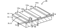
- FIG. 2 is a perspective view of the base substrate 14
- FIG. 3 is a plan view of the base substrate 14.
- GaN will be described as an example of the group 13 nitride.
- the crystal production apparatus 10 includes a growth container 12, a base substrate 14 disposed in the growth container 12, a reaction container 20 that stores the growth container 12, and the reaction container 20.
- An electric furnace 24 and a pressure controller 40 provided between the nitrogen cylinder 42 and the electric furnace 24 are provided.
- the growth container 12 is a bottomed cylindrical alumina crucible.
- a base substrate 14 is disposed in the growth container 12.
- the growth container 12 contains metal gallium and flux.
- metallic sodium is preferable.
- Metallic gallium and flux become a mixed melt when heated.
- the base substrate 14 is formed by epitaxially growing GaN having a predetermined thickness (for example, about several ⁇ m) on the sapphire substrate 15 by a vapor phase method to form a seed crystal layer 16.
- a vapor phase method to form a seed crystal layer 16.
- convex portions 16a and concave portions 16b are alternately provided in stripes.
- the convex portion 16a has a step ha of 0.3 to 40 ⁇ m (preferably 0.5 to 10 ⁇ m), a width wa of 5 to 100 ⁇ m (preferably 10 to 50 ⁇ m), and the concave portion 16b has a thickness tb of 2 ⁇ m or more.
- the width wb is 50 to 500 ⁇ m (preferably 100 to 250 ⁇ m). Further, as shown in FIG.
- the edge of the convex portion 16a is formed in parallel with the hexagonal a-plane of GaN.
- the main surface of the seed crystal layer 16 can be processed by, for example, dry etching, sand blasting, laser, dicing, or the like.
- dry etching For example, after covering a portion of the main surface corresponding to the convex portion 16a with a mask, the surface of the portion not covered with the mask is removed by dry etching. Thereby, the part removed by dry etching becomes the concave part 16b, and the part covered with the mask becomes the convex part 16a.
- the off angle ⁇ s is preferably 0.2 to 2 ° in the m-axis direction of sapphire (a-axis direction of GaN), and more preferably 0.3 to 1 °.
- the off angle ⁇ g is preferably 0.24 to 2.4 ° in the a-axis direction of GaN, and more preferably 0.36 to 1.2 °. .
- the reaction vessel 20 is made of stainless steel, and is placed on a disc-shaped turntable 50 having a rotary shaft 52 attached to the lower surface.
- the rotating shaft 52 has an internal magnet 54 and rotates as the external magnet 56 arranged in a ring shape outside the cylindrical casing 58 is rotated by an external motor (not shown).
- the inlet pipe 22 inserted into the reaction vessel 20 is cut in the upper zone 34. For this reason, when the rotation shaft 52 rotates, the reaction vessel 20 placed on the turntable 50 also rotates without any trouble. Further, nitrogen gas filled in the electric furnace 24 from the nitrogen cylinder 42 via the pressure controller 40 is introduced into the reaction vessel 20 from the inlet pipe 22.
- the electric furnace 24 includes a hollow cylindrical body 26 in which the reaction vessel 20 is disposed, and an upper lid 28 and a lower lid 30 that block the upper opening and the lower opening of the cylindrical body 26, respectively.
- the electric furnace 24 is a three-zone heater type, and is divided into three zones, an upper zone 34, an intermediate zone 35, and a lower zone 36, by two ring-shaped partition plates 32 and 33 provided on the inner wall of the cylindrical body 26. It has been. Further, an upper heater 44 is embedded in the inner wall surrounding the upper zone 34, a middle heater 45 is embedded in the inner wall surrounding the middle zone 35, and a lower heater 46 is embedded in the inner wall surrounding the lower zone 36. A bottom heater 47 is embedded in the interior.
- Each of the heaters 44 to 47 is controlled to have a target temperature set individually in advance by a heater control device (not shown).
- the reaction vessel 20 is accommodated so that the upper end is located in the upper zone 34 and the lower end is located in the lower zone 36.
- the lower lid 30 is integrated with the cylindrical casing 58.
- the pressure controller 40 performs control so that the pressure of the nitrogen gas supplied to the reaction vessel 20 becomes a preset target pressure.
- the base substrate 14 is prepared and placed in the growth container 12. At this time, the base substrate 14 may be disposed horizontally or obliquely. Moreover, metallic gallium and metallic sodium as a flux are prepared, and they are weighed so as to have a desired molar ratio and are accommodated in the growth vessel 12.
- the growth vessel 12 is put into the reaction vessel 20 and the electric furnace 24 is filled with nitrogen gas from the nitrogen cylinder 42 via the pressure controller 40. This nitrogen gas is introduced into the reaction vessel 20 from the inlet pipe 22.
- the reaction vessel 20 is placed on the turntable 50 so as to reach the lower zone 36 from the upper zone 34 in the cylindrical body 26 of the electric furnace 24, and the lower lid 30 and the upper lid 28 are closed. Then, while rotating the turntable 50 at a predetermined rotation speed, the pressure controller 40 controls the inside of the reaction vessel 20 to have a predetermined nitrogen gas pressure, and an upper heater 44 and an intermediate heater 45 are controlled by a heater control device (not shown). , The lower heater 46 and the bottom heater 47 are controlled to reach predetermined target temperatures, respectively, to grow a GaN crystal.
- the nitrogen gas pressure is preferably set to 1 to 7 MPa, more preferably 2 to 6 MPa.
- the average temperature of the four heaters is preferably set to 700 to 1000 ° C., more preferably set to 800 to 900 ° C.
- the growth time of the GaN crystal may be appropriately set according to the heating temperature and the pressure of the pressurized nitrogen gas, and may be set in the range of several hours to several hundred hours, for example.
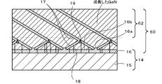
- FIG. 4 is a cross-sectional view of GaN grown on the seed crystal layer 16 of the base substrate 14.
- a convex portion 16a exists between the two concave portions 16b.
- the grain boundary 17 extends obliquely upward so as to cover one of the two concave portions 16b, starting from one edge of the convex portion 16a. Further, starting from the other edge of the same convex portion 16a, the grain boundary 17 extends obliquely upward so as to cover the other of the two concave portions 16b.
- Such extension of the grain boundary 17 occurs at each convex portion 16a. Therefore, the grain boundaries 17 generated from the adjacent convex portions 16a collide in the middle.
- Grain boundaries 17 generated from the protrusions 16a grow while involving inclusions, but at the locations where the grain boundaries 17 collide with each other, voids 19 (including inclusions) are formed and the inclusions converge. For this reason, GaN having no (or almost no) inclusion grows in the upper layer portion above the portion where the grain boundaries 17 collide with each other.
- the plurality of voids 19 formed at the locations where the grain boundaries 17 collide with each other play a role in relieving thermal stress caused by the difference in thermal expansion between the sapphire substrate 15 and GaN, cracks are generated in the grown GaN. To suppress.
- the dislocations 18 included in the seed crystal layer 16 propagate in a direction intersecting with the direction in which the grain boundary 17 travels (direction perpendicular (or nearly perpendicular) to the main surface), and the grain boundary 17 and the dislocation 18 intersect.
- the propagation of the dislocation 18 at the point is stopped by the grain boundary 17, and the dislocation 18 does not propagate beyond the grain boundary 17. Therefore, the group 13 nitride crystal grown above the void 19 has a high quality with reduced inclusions, cracks, and dislocations 18.
- the sapphire substrate 15 is removed from the GaN substrate 60 by laser lift-off, and the surface on the seed crystal side of the obtained GaN substrate 60 is polished until the void 19 disappears (to the position of the one-dot chain line in FIG. 4).
- the polished GaN substrate 62 is a uniform (or almost uniform) GaN substrate free from inclusions and cracks.
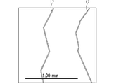
- FIG. 5 shows a state where the upper surface (the surface opposite to the seed crystal) of the GaN substrate 62 is observed. As shown in FIG. 5, the grain boundary 17 appears in a bent shape on the upper surface of the grown GaN.
- the seed crystal layer 16 of the base substrate 14 is not a stepped step as in the prior art, but has a structure in which the convex portions 16a and the concave portions 16b are repeatedly provided in a stripe shape. Therefore, a high-quality GaN substrate 62 can be manufactured by the flux method even if the seed crystal layer 16 has a thin base substrate 14.
- the base substrate 14 in which the edge of the convex portion 16a is parallel to the hexagonal a-plane of GaN is used, but the base substrate in which the edge of the convex portion 16a is parallel to the m-plane of hexagonal crystal of GaN. May be used.
- the edge of the convex portion 16a is parallel to the a-plane of GaN hexagonal crystal because the angle of the grain boundary 17 with respect to the c-plane is small and the thickness of the discarded portion of the GaN substrate 60 is small.
- Example 1 (Typical Example) (Preparation of base substrate)
- the seed substrate 16 was formed by epitaxially growing GaN having a thickness of 8 ⁇ m on the sapphire substrate 15 having an off angle of 0.5 ° in the m-axis direction of the sapphire by vapor phase deposition.
- a concavo-convex pattern was formed on the surface of the seed crystal layer 16 of the base substrate 14 by dry etching (here, RIE) so as to form a stripe parallel to the a-plane of GaN.
- dry etching here, RIE
- the step ha (height) of the convex portion 16a was 5 ⁇ m
- the width wa of the convex portion 16a was 15 ⁇ m
- the width wb of the concave portion 16b was 150 ⁇ m
- the thickness tb of the concave portion 16b was 3 ⁇ m.
- GaN substrate production A GaN substrate 60 was produced by growing a GaN crystal on the seed crystal layer 16 of the base substrate 14 using the crystal manufacturing apparatus 10 having a pressure vessel structure shown in FIG. First, in the glove box of nitrogen atmosphere, the base substrate 14 was horizontally arranged on the bottom of the alumina crucible as the growth container 12 so that the seed crystal layer 16 was on the top. A crucible was filled with 80 g of metallic sodium and 50 g of metallic gallium and covered with an alumina plate. The crucible was placed in a stainless steel inner container (not shown in FIG. 1), and further placed in a stainless outer container, which is a reaction container 20 that can accommodate the crucible, and closed with a container lid with an inlet pipe 22. .
- This outer container was placed on a turntable 50 installed in a heating unit in the crystal manufacturing apparatus 10 that had been vacuum-baked in advance, and the pressure vessel, which is the cylindrical body 26, was covered and sealed. And the inside of the pressure vessel was evacuated to 0.1 Pa or less by a vacuum pump. Subsequently, while adjusting the upper heater 44, the middle heater 45, the lower heater 46, and the bottom heater 47 so that the temperature of the heating space becomes 870 ° C., nitrogen gas is introduced from the nitrogen cylinder 42 to 4.0 MPa. The outer container was rotated clockwise and counterclockwise at a constant cycle at a speed of 20 rpm around the central axis.
- the polished GaN substrate 62 was observed with an epi-illumination optical microscope to inspect the uniformity. When observed with an epi-illumination optical microscope, the portion where the inclusion exists appears to shine. In the GaN substrate 62 of Experimental Example 1, it was determined that there was no portion that looked shining and there was no inclusion.
- Table 1 summarizes the concavo-convex pattern of the base substrate 14 of Experimental Example 1 and the evaluation results of the obtained GaN substrates 60 and 62.
- a high-quality GaN substrate 62 that is low and free of inclusion was obtained (Experimental Example 9).
- the width wa of the convex portion 16a is wide, so that the dislocation density in the upper region of the convex portion 16a is not substantially zero, but the dislocation density is relatively low and no inclusion is observed.
- a substrate 62 was obtained (Experimental Example 12). Further, when the width wa of the convex portion 16a was in the range of 10 to 50 ⁇ m, a high quality GaN substrate 62 having a low dislocation density and no cracks or inclusions was obtained (Experimental Examples 1, 10, and 11).
- the convex portion 16a disappears in the middle due to meltback, and grain boundaries did not occur, so the entire surface was not lowered, and no voids were generated.
- the substrate 60 was cracked (Experimental Example 8). If the upper limit is exceeded, the convex portion 16a is too wide although there is a grain boundary, and the upper region of the convex portion 16a does not become low dislocation, and although there is a void, the distribution density of the void is low, so the stress relaxation effect is insufficient and the GaN The substrate 60 was broken (Experimental Example 13).
- the width wa of the convex portion 16a exceeds 100 ⁇ m as in Experimental Example 13, the thickness of the GaN to be grown is increased, and the grain boundary 17 (grain boundary 17 after collision) immediately above the convex portion 16a. Is obliquely crossed, the dislocation directed upward from the upper surface of the convex portion 16a is stopped by the grain boundary, so that the dislocation does not propagate further upward. In this case, although the amount of polishing the surface on the seed crystal side is increased, the polished GaN substrate is of high quality.
- the internal crack was generated because the void distribution density was slightly small, but a high-quality GaN substrate 62 having a low dislocation density and no inclusion was obtained except for the location of the internal crack (Experimental Example 21). Further, when the width wb of the recess 16b was in the range of 100 to 250 ⁇ m, a high quality GaN substrate 62 having a low dislocation density and no cracks or inclusions was obtained (Experimental Examples 1, 19, and 20). On the other hand, when the value was below the lower limit (Experimental Example 17), voids were not generated well, so the stress relaxation effect was not obtained and the GaN substrate 60 was cracked. In addition, many grain boundaries including inclusions remained in the upper layer. When the upper limit was exceeded (Experimental Example 22), the void distribution density was small and the void size was large, and the GaN substrate 60 was cracked. In addition, many inclusions remained in the upper layer.
- the GaN substrate 62 obtained in each experimental example emits broad fluorescence (blue fluorescence) having a peak at 440 to 470 nm when irradiated with light having a wavelength of 330 to 385 nm (for example, light from a mercury lamp).
- a GaN crystal produced by a flux method generally emits blue light when irradiated with light of this wavelength.
- a GaN crystal produced by a vapor phase method emits yellow fluorescence when irradiated with similar light. For this reason, it is possible to distinguish between the crystal by the flux method and the crystal by the vapor phase method by the color of the fluorescence emitted when the light of this wavelength is irradiated.
- the present invention is applicable to a method for producing a group 13 nitride crystal typified by gallium nitride.
Landscapes
- Engineering & Computer Science (AREA)
- Chemical & Material Sciences (AREA)
- Crystallography & Structural Chemistry (AREA)
- Physics & Mathematics (AREA)
- Power Engineering (AREA)
- Microelectronics & Electronic Packaging (AREA)
- Computer Hardware Design (AREA)
- Condensed Matter Physics & Semiconductors (AREA)
- General Physics & Mathematics (AREA)
- Manufacturing & Machinery (AREA)
- Materials Engineering (AREA)
- Metallurgy (AREA)
- Organic Chemistry (AREA)
- Inorganic Chemistry (AREA)
- Chemical Kinetics & Catalysis (AREA)
- General Chemical & Material Sciences (AREA)
- Plasma & Fusion (AREA)
- Crystals, And After-Treatments Of Crystals (AREA)
- Recrystallisation Techniques (AREA)
Abstract
本発明の一実施形態である下地基板14は、サファイヤ基板15上に13族窒化物の種結晶層16を備えている。種結晶層16の主面には、凸部16aと凹部16bとがストライプ状に繰り返し現れ、凸部16aの段差haは0.3~40μm、凸部16aの幅waは5~100μm、凹部16bの厚みtbは2μm以上、凹部16bの幅wbは50~500μmである。
Description
本発明は、下地基板、下地基板の製法及び13族窒化物結晶の製法に関する。
窒化ガリウム結晶に代表される13族窒化物結晶をフラックス法で作製する際に用いる下地基板として、その下地基板の種結晶層の主面にマイクロステップを階段状に設けたものが知られている(特許文献1参照)。この下地基板を用いてGaN結晶を成長させる手順は、以下の通りである。すなわち、GaNの種結晶層を備えた下地基板を金属ガリウムと金属ナトリウムとを含む混合融液へ浸漬し、その混合融液へ窒素ガスを導入しながら下地基板の主面上にGaN結晶を成長させる。主面上にGaN結晶が成長していく際、ステップの段差付近を起点として粒界が斜め上方に向かって発生する。一方、種結晶層に含まれる転位は、粒界の進む方向と交差する方向に伝搬し、粒界と転位とが交差した地点で転位の伝搬は粒界によって止められる。したがって、この下地基板を用いてフラックス法により作製したGaN結晶のうち上層部分はほとんど転位による欠陥のないものとなる。
しかしながら、上述の下地基板では、マイクロステップを階段状に設けたため、ある程度の厚みをもった種結晶層が必要になるという問題があった。
本発明はこのような課題を解決するためになされたものであり、種結晶層の厚さが薄くても転位による欠陥の少ない13族窒化物結晶をフラックス法で作製可能な下地基板を提供することを主目的とする。
本発明は、上述の主目的を達成するために以下の手段を採った。
本発明の下地基板は、
13族窒化物の種結晶層を備えた下地基板であって、
前記種結晶層の主面には、凸部と凹部とがストライプ状に繰り返し現れ、
前記凸部の段差は0.3~40μm、前記凸部の幅は5~100μm、前記凹部の厚みは2μm以上、前記凹部の幅は50~500μm
のものである。
13族窒化物の種結晶層を備えた下地基板であって、
前記種結晶層の主面には、凸部と凹部とがストライプ状に繰り返し現れ、
前記凸部の段差は0.3~40μm、前記凸部の幅は5~100μm、前記凹部の厚みは2μm以上、前記凹部の幅は50~500μm
のものである。
この下地基板は、例えば以下のようにしてフラックス法に使用される。すなわち、下地基板を13族金属とフラックスと共に容器に入れ、その容器へ窒素ガスを導入しながら加熱することにより下地基板の種結晶層の主面上に13族窒化物結晶を成長させる。ここで、種結晶層上には、二つの凹部の間に一つの凸部が存在している。種結晶層上に13族窒化物結晶が成長していくと、その凸部の一方のエッジ付近を起点として、二つの凹部のうちの一方を覆うように斜め上向きに粒界が伸展していく。また、同じ凸部のもう一方のエッジ付近を起点として、二つの凹部のうちのもう一方を覆うように斜め上向きに粒界が伸展していく。このような粒界の伸展は、各凸部で起こる。互いに隣同士の凸部から発生した粒界は途中で衝突する。凸部から発生する粒界はインクルージョンを巻き込みながら成長していくが、粒界同士が衝突した箇所ではボイド(インクルージョンを内包している)が形成されてインクルージョンが収束する。そのため、粒界同士が衝突した箇所よりも上側の上層部にはインクルージョンのない(又はほとんどない)13族窒化物結晶が成長する。また、粒界同士が衝突した箇所に形成された多数のボイドは、下地基板のうち種結晶層と種結晶層以外の層との熱膨張差に起因する熱応力を緩和する役割を果たすため、成長した13族窒化物にクラックが発生するのを抑制する。一方、種結晶層に含まれる転位は、粒界の進む方向と交差する方向に伝搬し、粒界と転位とが交差した地点で転位の伝搬は粒界によって止められ、粒界を超えて上方へ転位が伝搬することはない。したがって、得られた13族窒化物結晶のうちボイドよりも上側の上層部は、インクルージョンやクラック、転位の低減された高品質なものとなる。そのため、得られた13族窒化物結晶のうちボイドよりも下側の下層部(種結晶層を含む)を研磨などで除去することにより、高品質の13族窒化物結晶を得ることができる。以上のように、本発明の下地基板によれば、従来のように階段状のステップではなく、凸部と凹部とをストライプ状になるように繰り返し設けた構造であるため、種結晶層の厚さが薄くても高品質な13族窒化物結晶をフラックス法で作製することができる。
凸部の段差は0.3~40μm、凸部の幅は5~100μmであることが好ましい。凸部の段差が0.3μm未満だと、フラックス法により得られた13族窒化物結晶に粒界が発生しないため全面的に低転位化しないし、ボイドも発生しないため応力緩和効果が得られず結晶が割れてしまうことがある。凸部の段差が40μmを超えると、フラックス法により得られた13族窒化物結晶の上層部にボイドが残り、そのボイドを起点として結晶が割れてしまうことがある。凸部の幅が5μm未満だと、フラックス法の途中でメルトバックにより凸部が消失してしまい、粒界が発生しないため全面的に低転位化しないし、ボイドも発生しないため応力緩和効果が得られず結晶が割れてしまうことがある。凸部の幅が100μmを超えると、フラックス法により得られた13族窒化物結晶のうち凸部の上方領域が低転位化しないし、ボイドの分布密度が低いため応力緩和効果が不十分で結晶が割れてしまうことがある。
凹部の厚みは2μm以上、凹部の幅は50~500μmであることが好ましい。凹部の厚みが2μm未満だと、途中でメルトバックにより種結晶層が消失してしまうため、13族窒化物結晶が成長しない。凹部の厚みの上限は特に限定するものではないが、少なくとも40μmまでは本発明の効果が得られることは確認済みである。凹部の幅が50μm未満だと、ボイドがうまく生成しなかったりボイドが生成したとしてもサイズが大きかったりするため、結晶が割れたり上層部にインクルージョンが多く残ったりする。凹部の幅が500μmを超えると、ボイドの分布密度が少なく且つボイドのサイズが大きいため、結晶が割れたり上層部にインクルージョンが多く残ったりする。
ここで、13族窒化物としては、窒化ホウ素(BN)、窒化アルミニウム(AlN)、窒化ガリウム(GaN)、窒化インジウム(InN)、窒化タリウム(TlN)などが挙げられるが、このうちGaNが好ましい。下地基板としては、例えば、サファイヤ基板やシリコンカーバイド基板、シリコン基板などの表面に13族窒化物と同じ種類の薄膜が種結晶層として形成されたものを用いてもよいし、13族窒化物と同じ種類の基板を用いてもよいが、サファイヤ基板が好ましい。なお、フラックスとしては、各種金属の中から13族金属の種類に応じて適宜選択すればよく、例えば13族金属がガリウムの場合にはアルカリ金属が好ましく、金属ナトリウムや金属カリウムがより好ましく、金属ナトリウムが更に好ましい。インクルージョンとは、主として13族窒化物の結晶中に取り込まれた混合融液(13族金属とフラックスとの融液)が固化したものである。
本発明の下地基板において、前記凸部の段差は0.5~10μm、前記凸部の幅は10~50μm、前記凹部の幅は100~250μmであることが好ましい。こうすれば、この下地基板を用いてフラックス法により得られた13族窒化物結晶の上層部(ボイドよりも上側)は、より高品質なものとなる。
本発明の下地基板において、前記凸部のエッジは、前記13族窒化物結晶のa面に平行であることが好ましい。凸部のエッジが13族窒化物結晶のa面に平行な場合には、m面に平行な場合よりも、c面に対して粒界のなす角度が小さくなるため、粒界が衝突して形成されるボイドの位置が低くなる。その結果、成長した13族窒化物結晶のうち廃棄する厚みが少なくなり、歩留まりが良くなる。なお、「a面に平行」とは、a面に完全に平行な場合のほか、a面に実質的に平行な場合(例えばa面と5°未満の角度をなす方向)も含む。
本発明の下地基板において、前記種結晶層は、オフ角が前記13族窒化物結晶のa軸方向に0.24~2.4°であることが好ましい。オフ角がこの範囲であれば、フラックス法により得られた13族窒化物結晶の上層部に部分的にクラックが内在することがあるが、そのクラックの入った箇所を除けば十分高品質な13族窒化物結晶が得られる。このオフ角は前記13族窒化物結晶のa軸方向に0.36~1.2°であることがより好ましい。オフ角がこの範囲であれば、クラックのない(又はほとんどない)13族窒化物結晶が得られる。
本発明の下地基板の製法は、
上述したいずれかの下地基板を作製する方法であって、
サファイヤ基板上に気相法で前記種結晶層となる13族窒化物をエピタキシャル成長させて成膜し、前記種結晶層の主面に、前記凸部と前記凹部とがストライプ状に繰り返し現れるようにパターニングすることにより下地基板を得る、
ものである。
上述したいずれかの下地基板を作製する方法であって、
サファイヤ基板上に気相法で前記種結晶層となる13族窒化物をエピタキシャル成長させて成膜し、前記種結晶層の主面に、前記凸部と前記凹部とがストライプ状に繰り返し現れるようにパターニングすることにより下地基板を得る、
ものである。
この製法によれば、上述した下地基板を比較的容易に作製することができる。ここで、パターニングの方法としては、特に限定するものではないが、例えばドライエッチング、ウェットエッチング、レーザー加工、サンドブラスト加工、EB蒸着、ダイシングなどが挙げられる。このうち、ドライエッチングが好ましい。
本発明の13族窒化物結晶の製法は、
上述したいずれかの下地基板を13族金属と金属ナトリウムと共に容器に入れ、前記容器に窒素を導入しながら700~1000℃に加熱することにより、前記種結晶層上に13族窒化物結晶を成長させる、
ものである。
上述したいずれかの下地基板を13族金属と金属ナトリウムと共に容器に入れ、前記容器に窒素を導入しながら700~1000℃に加熱することにより、前記種結晶層上に13族窒化物結晶を成長させる、
ものである。
この製法によれば、高品質な13族窒化物結晶を得ることができる。具体的には、種結晶層上には、二つの凹部の間に一つの凸部が存在している。種結晶層上に13族窒化物結晶が成長していくと、その凸部の一方のエッジ付近を起点として、二つの凹部のうちの一方を覆うように斜め上向きに粒界が伸展していく。また、同じ凸部のもう一方のエッジ付近を起点として、二つの凹部のうちのもう一方を覆うように斜め上向きに粒界が伸展していく。このような粒界の伸展は、各凸部で起こる。互いに隣同士の凸部から発生した粒界は途中で衝突する。凸部から発生する粒界はインクルージョンを巻き込みながら成長していくが、粒界同士が衝突した箇所ではボイド(インクルージョンを内包している)が形成されてインクルージョンが収束する。そのため、粒界同士が衝突した箇所よりも上側の上層部にはインクルージョンのない(又はほとんどない)13族窒化物結晶が成長する。また、粒界同士が衝突した箇所に形成された多数のボイドは、下地基板のうち種結晶層と種結晶層以外の層との熱膨張差に起因する熱応力を緩和する役割を果たすため、成長した13族窒化物にクラックが発生するのを抑制する。一方、種結晶層に含まれる転位は、粒界の進む方向と交差する方向に伝搬し、粒界と転位とが交差した地点で転位の伝搬は粒界によって止められ、粒界を超えて上方へ転位が伝搬することはない。したがって、得られた13族窒化物結晶のうちボイドよりも上側の上層部は、インクルージョンやクラック、転位の低減された高品質なものとなる。そのため、得られた13族窒化物結晶のうちボイドよりも下側の下層部(種結晶層を含む)を研磨などで除去することにより、高品質の13族窒化物結晶を得ることができる。以上のように、本発明の13族窒化物結晶の製法によれば、下地基板の種結晶層の厚さが薄くても高品質な13族窒化物結晶を得ることができる。
この製法によって得られる13族窒化物結晶は、転位密度が1×10⁶/cm2以下であることが好ましく、1×104/cm2未満であることがより好ましい。
本発明の13族窒化物結晶の成長方法を実施するための好適な装置について、図面を用いて以下に説明する。図1は結晶製造装置10の全体構成を示す説明図、図2は下地基板14の斜視図、図3は下地基板14の平面図である。以下には、13族窒化物としてGaNを例に挙げて説明する。
結晶製造装置10は、図1に示すように、育成容器12と、この育成容器12に配置される下地基板14と、育成容器12を収納する反応容器20と、この反応容器20が配置される電気炉24と、窒素ボンベ42と電気炉24との間に設けられた圧力制御器40とを備えている。
育成容器12は、有底筒状でアルミナ製の坩堝である。この育成容器12には、下地基板14が配置される。また、育成容器12には、金属ガリウムとフラックスが収容される。フラックスとしては、金属ナトリウムが好ましい。金属ガリウムとフラックスは、加熱することにより混合融液となる。
下地基板14は、図2に示すように、サファイヤ基板15上に気相法により所定厚さ(例えば数μm程度)のGaNをエピタキシャル成長させて成膜して種結晶層16を形成したあと、種結晶層16の主面に凸部16aと凹部16bとをストライプ状に交互に設けたものである。凸部16aは、段差haが0.3~40μm(好ましくは0.5~10μm)、幅waが5~100μm(好ましくは10~50μm)であり、凹部16bは、厚さtbが2μm以上、幅wbが50~500μm(好ましくは100~250μm)である。また、図3に示すように、凸部16aのエッジがGaNの六方晶のa面と平行に形成されている。こうした種結晶層16の主面の加工は、例えば、ドライエッチング、サンドブラスト、レーザー、ダイシング等によって行うことができる。例えば、主面のうち凸部16aに相当する箇所をマスクで覆った後、マスクで覆われていない箇所の表面をドライエッチングで除去する。これにより、ドライエッチングで除去された箇所が凹部16bとなり、マスクで覆われていた箇所が凸部16aとなる。また、主面の法線とサファイヤ基板のc軸とのオフ角θsと、主面の法線とGaNの種結晶層のc軸とのオフ角θgとの間には、θg≒1.2θsの関係式が成り立つことが知られている。オフ角θsはサファイヤのm軸方向(GaNのa軸方向)に0.2~2°が好ましく、0.3~1°がより好ましい。これを先の関係式によりオフ角θgに換算すると、オフ角θgはGaNのa軸方向に0.24~2.4°が好ましく、0.36~1.2°がより好ましいということになる。
反応容器20は、ステンレス製であり、下面に回転シャフト52が取り付けられた円盤状の回転台50の上に載置されている。回転シャフト52は、内部磁石54を有しており、筒状ケーシング58の外側にリング状に配置された外部磁石56が図示しない外部モーターによって回転するのに伴って回転する。反応容器20に差し込まれたインレットパイプ22は、上ゾーン34内で切断されている。このため、回転シャフト52が回転すると、回転台50の上に載置された反応容器20も支障なく回転する。また、窒素ボンベ42から圧力制御器40を介して電気炉24内に充満された窒素ガスは、インレットパイプ22から反応容器20内に導入される。
電気炉24は、内部に反応容器20が配置される中空の円筒体26と、この円筒体26の上部開口及び下部開口をそれぞれ塞ぐ上蓋28及び下蓋30とを備えている。この電気炉24は、3ゾーンヒーター式であり、円筒体26の内壁に設けられたリング状の2つの仕切り板32,33により、上ゾーン34、中ゾーン35、下ゾーン36の3つに分けられている。また、上ゾーン34を取り囲む内壁には上ヒーター44が埋設され、中ゾーン35を取り囲む内壁には中ヒーター45が埋設され、下ゾーン36を取り囲む内壁には下ヒーター46が埋設され、下蓋30には底部ヒーター47が埋設されている。各ヒーター44~47は、図示しないヒーター制御装置により予め個別に設定された目標温度となるように制御される。なお、反応容器20は、上端が上ゾーン34、下端が下ゾーン36に位置するように収容される。また、下蓋30は、筒状ケーシング58と一体化されている。
圧力制御器40は、反応容器20へ供給する窒素ガスの圧力が予め設定された目標圧力になるように制御する。
このようにして構成された本実施形態の結晶製造装置10の使用例について説明する。まず、下地基板14を用意し、育成容器12に入れる。このとき、下地基板14を水平に配置してもよいし斜めに配置してもよい。また、金属ガリウムとフラックスとしての金属ナトリウムを用意し、それらを所望のモル比となるように秤量し育成容器12に収容する。この育成容器12を反応容器20に入れ、窒素ボンベ42から圧力制御器40を介して電気炉24内に窒素ガスを充満させる。この窒素ガスは、インレットパイプ22から反応容器20内に導入される。この反応容器20を電気炉24の円筒体26内の上ゾーン34から中ゾーン35を経て下ゾーン36に至るように回転台50の上に載置し、下蓋30及び上蓋28を閉じる。そして、所定の回転速度で回転台50を回転させながら、圧力制御器40により反応容器20内が所定の窒素ガス圧となるように制御し、図示しないヒーター制御装置により上ヒーター44,中ヒーター45,下ヒーター46,底部ヒータ-47をそれぞれ所定の目標温度となるように制御し、GaN結晶を成長させる。窒素ガス圧は、1~7MPaに設定するのが好ましく、2~6MPaに設定するのがより好ましい。また、4つのヒーターの平均温度は700~1000℃に設定するのが好ましく、800~900℃に設定するのがより好ましい。GaN結晶の成長時間は、加熱温度や加圧窒素ガスの圧力に応じて適宜設定すればよく、例えば数時間~数100時間の範囲で設定すればよい。
図4は下地基板14の種結晶層16上に成長したGaNの断面図である。種結晶層16上には、二つの凹部16bの間に凸部16aが存在している。種結晶層16上にGaNが成長していくと、凸部16aの一方のエッジを起点として、二つの凹部16bのうちの一方を覆うように斜め上向きに粒界17が伸展していく。また、同じ凸部16aのもう一方のエッジを起点として、二つの凹部16bのうちのもう一方を覆うように斜め上向きに粒界17が伸展していく。このような粒界17の伸展は、各凸部16aで起こる。そのため、互いに隣同士の凸部16aから発生した粒界17は途中で衝突する。凸部16aから発生する粒界17はインクルージョンを巻き込みながら成長していくが、粒界17同士が衝突した箇所ではボイド19(インクルージョンを内包している)が形成されてインクルージョンが収束する。そのため、粒界17同士が衝突した箇所よりも上側の上層部にはインクルージョンのない(又はほとんどない)GaNが成長する。また、粒界17同士が衝突した箇所に形成された複数のボイド19は、サファイヤ基板15とGaNとの熱膨張差に起因する熱応力を緩和する役割を果たすため、成長したGaNにクラックが発生するのを抑制する。一方、種結晶層16に含まれる転位18は、粒界17の進む方向と交差する方向(主面に垂直(又はほぼ垂直)な方向)に伝搬し、粒界17と転位18とが交差した地点で転位18の伝搬は粒界17によって止められ、粒界17を超えて転位18が伝搬することはない。したがって、ボイド19よりも上側に成長した13族窒化物結晶は、インクルージョンやクラック、転位18の低減された高品質なものとなる。GaNを成長させた後、レーザーリフトオフによりサファイヤ基板15をGaN基板60から外し、得られたGaN基板60のうち種結晶側の面をボイド19がなくなるまで(図4の一点鎖線の位置まで)研磨する。研磨後のGaN基板62は、インクルージョンやクラックのない均一な(又はほぼ均一な)GaN基板となる。GaN基板62の上面(種結晶とは反対側の面)を観察した様子を図5に示す。図5に示すように、成長したGaNの上面では、粒界17は曲折した形状に現れる。
以上詳述した本実施形態によれば、下地基板14の種結晶層16は従来のように階段状のステップではなく、凸部16aと凹部16bとをストライプ状になるように繰り返し設けた構造であるため、種結晶層16の厚さが薄い下地基板14でも高品質なGaN基板62をフラックス法で作製することができる。
なお、本発明は上述した実施形態に何ら限定されることはなく、本発明の技術的範囲に属する限り種々の態様で実施し得ることはいうまでもない。
例えば、上述した実施形態では、凸部16aのエッジがGaNの六方晶のa面と平行な下地基板14を用いたが、凸部16aのエッジがGaNの六方晶のm面と平行な下地基板を用いてもよい。但し、凸部16aのエッジがGaNの六方晶のa面と平行な方が、c面に対する粒界17の角度が小さくGaN基板60のうち廃棄する部分の厚みが小さくなるため好ましい。
以下に、本発明の実施例について説明する。なお、以下の実施例は本発明を何ら限定するものではない。
[実験例1](典型的な実施例)
(下地基板作製)
オフ角がサファイヤのm軸方向に0.5°のサファイヤ基板15上に、気相法で厚さ8μmのGaNをエピタキシャル成長させて種結晶層16を成膜することにより、下地基板14を作製した。その下地基板14の種結晶層16の表面に、GaNのa面に平行なストライプ状となるように凹凸パターンをドライエッチング(ここではRIE)により作製した。凹凸パターンは、凸部16aの段差ha(高さ)を5μm、凸部16aの幅waを15μm、凹部16bの幅wbを150μm、凹部16bの厚さtbを3μmとした。
(下地基板作製)
オフ角がサファイヤのm軸方向に0.5°のサファイヤ基板15上に、気相法で厚さ8μmのGaNをエピタキシャル成長させて種結晶層16を成膜することにより、下地基板14を作製した。その下地基板14の種結晶層16の表面に、GaNのa面に平行なストライプ状となるように凹凸パターンをドライエッチング(ここではRIE)により作製した。凹凸パターンは、凸部16aの段差ha(高さ)を5μm、凸部16aの幅waを15μm、凹部16bの幅wbを150μm、凹部16bの厚さtbを3μmとした。
(GaN基板作製)
図1に示す耐圧容器構造の結晶製造装置10を用いて、下地基板14の種結晶層16上にGaN結晶を成長させることによりGaN基板60を作製した。まず、窒素雰囲気のグローブボックス内で、育成容器12であるアルミナ坩堝の底に下地基板14を種結晶層16が上になるように水平に配置した。金属ナトリウム80g、金属ガリウム50gを坩堝内に充填し、アルミナ板で蓋をした。その坩堝をステンレス製の内容器(図1には図示せず)に入れ、さらにそれを収納できる反応容器20であるステンレス製の外容器に入れて、インレットパイプ22の付いた容器蓋で閉じた。この外容器を、予め真空ベークしてある結晶製造装置10内の加熱部に設置されている回転台50の上に配置し、円筒体26である耐圧容器に蓋をして密閉した。そして、耐圧容器内を真空ポンプにて0.1Pa以下まで真空引きした。続いて、上ヒーター44、中ヒーター45、下ヒーター46及び底部ヒータ47を調節して加熱空間の温度を870℃になるように加熱しながら、4.0MPaまで窒素ボンベ42から窒素ガスを導入し、外容器を中心軸周りに20rpmの速度で一定周期の時計回りと反時計回りで回転させた。加速時間=12秒、保持時間=600秒、減速時間=12秒、停止時間=0.5秒とした。そして、この状態で50時間保持した。その後、室温まで自然冷却して大気圧に戻した後、耐圧容器の蓋を開けて中から坩堝を取り出した。坩堝の中の固化した金属ナトリウムを除去し、サファイヤ基板15と一体になったGaN基板60を回収し、レーザーリフトオフでサファイヤ基板15を除去し、自立化したGaN基板を得た。育成後のGaNにクラックはなかった。得られたGaN基板の表面及び裏面を研磨加工した。裏面(種結晶層側の面)はボイドや転位を含む厚さ約50μmの層を除去した。こうすることによりGaN基板62を得た。
図1に示す耐圧容器構造の結晶製造装置10を用いて、下地基板14の種結晶層16上にGaN結晶を成長させることによりGaN基板60を作製した。まず、窒素雰囲気のグローブボックス内で、育成容器12であるアルミナ坩堝の底に下地基板14を種結晶層16が上になるように水平に配置した。金属ナトリウム80g、金属ガリウム50gを坩堝内に充填し、アルミナ板で蓋をした。その坩堝をステンレス製の内容器(図1には図示せず)に入れ、さらにそれを収納できる反応容器20であるステンレス製の外容器に入れて、インレットパイプ22の付いた容器蓋で閉じた。この外容器を、予め真空ベークしてある結晶製造装置10内の加熱部に設置されている回転台50の上に配置し、円筒体26である耐圧容器に蓋をして密閉した。そして、耐圧容器内を真空ポンプにて0.1Pa以下まで真空引きした。続いて、上ヒーター44、中ヒーター45、下ヒーター46及び底部ヒータ47を調節して加熱空間の温度を870℃になるように加熱しながら、4.0MPaまで窒素ボンベ42から窒素ガスを導入し、外容器を中心軸周りに20rpmの速度で一定周期の時計回りと反時計回りで回転させた。加速時間=12秒、保持時間=600秒、減速時間=12秒、停止時間=0.5秒とした。そして、この状態で50時間保持した。その後、室温まで自然冷却して大気圧に戻した後、耐圧容器の蓋を開けて中から坩堝を取り出した。坩堝の中の固化した金属ナトリウムを除去し、サファイヤ基板15と一体になったGaN基板60を回収し、レーザーリフトオフでサファイヤ基板15を除去し、自立化したGaN基板を得た。育成後のGaNにクラックはなかった。得られたGaN基板の表面及び裏面を研磨加工した。裏面(種結晶層側の面)はボイドや転位を含む厚さ約50μmの層を除去した。こうすることによりGaN基板62を得た。
(評価)
・研磨加工前のGaN基板60の評価
研磨加工前のGaN基板60の断面の光学顕微鏡(OM)像、カソードルミネッセンス(CL)像及び走査電子顕微鏡(SEM)像を用いて、粒界、ボイド及びインクルージョンの検査を行った。そうしたところ、実験例1のGaN基板60は、図4に示すように、凸部16aのエッジから斜め上向きに粒界17が伸展してその粒界17と向かい合う粒界17とが衝突してボイド19を形成し、ボイド19よりも上層には2つの粒界17のうちの片方のみがインクルージョンを巻き込むことなく伸展している様子を確認することができた。
・研磨加工前のGaN基板60の評価
研磨加工前のGaN基板60の断面の光学顕微鏡(OM)像、カソードルミネッセンス(CL)像及び走査電子顕微鏡(SEM)像を用いて、粒界、ボイド及びインクルージョンの検査を行った。そうしたところ、実験例1のGaN基板60は、図4に示すように、凸部16aのエッジから斜め上向きに粒界17が伸展してその粒界17と向かい合う粒界17とが衝突してボイド19を形成し、ボイド19よりも上層には2つの粒界17のうちの片方のみがインクルージョンを巻き込むことなく伸展している様子を確認することができた。
また、研磨加工前のGaN基板60が割れているか否か、GaN基板60に内在クラックがあるか否かを、いずれも目視で確認した。そうしたところ、実験例1のGaN基板60には割れも内在クラックもみられなかった。
・研磨加工後のGaN基板62の評価
研磨加工したGaN基板62を、CL観察検出器付きのSEMで転位密度測定を行った。GaN基板62をCL観察すると、転位箇所が発光せずに黒点(ダークスポット)として観察される。そのダークスポット密度を計測することにより、転位密度が算出される。実験例1のGaN基板62の100μm角の領域を観察した結果、下地基板14の凸部16aの上方領域および凹部16bの上方領域ともにダークスポットは1つも観察されず、転位密度が1×10⁴/cm2未満であることが確認された。
研磨加工したGaN基板62を、CL観察検出器付きのSEMで転位密度測定を行った。GaN基板62をCL観察すると、転位箇所が発光せずに黒点(ダークスポット)として観察される。そのダークスポット密度を計測することにより、転位密度が算出される。実験例1のGaN基板62の100μm角の領域を観察した結果、下地基板14の凸部16aの上方領域および凹部16bの上方領域ともにダークスポットは1つも観察されず、転位密度が1×10⁴/cm2未満であることが確認された。
また、研磨加工したGaN基板62を落射型光学顕微鏡で観察して均一性の検査を行った。落射型光学顕微鏡で観察すると、インクルージョンの存在している部分は光って見える。実験例1のGaN基板62では、光って見える箇所はなく、インクルージョンのない均一な状態であると判断した。
以上の評価結果から、実験例1のGaN基板62の総合評価を「極めて良好」(◎)とした。なお、実験例1の下地基板14の凹凸パターンや得られたGaN基板60,62の評価結果を表1にまとめた。

[実験例2~7]
凸部16aの段差haを表1のように設定した以外は、実験例1と同様にして下地基板作製、GaN基板作製及び評価を行った。その結果を表1に示す。表1から明らかなように、凸部16aの段差haが0.3~40μmの範囲であれば、高品質のGaN基板62が得られた(実験例3~6)。但し、下限では、部分的にボイドが生成せず内在クラックが発生したが、内在クラックの箇所を除けば転位密度が低くインクルージョンもみられない高品質のGaN基板62が得られた(実験例3)。また、上限では、ボイドがやや大きくてそこから内在クラックが発生したが、内在クラックの箇所を除けば転位密度が低くインクルージョンもみられない高品質のGaN基板62が得られた(実験例6)。また、凸部16aの段差haが0.5~10μmの範囲であれば、転位密度が低くクラックもインクルージョンもみられない高品質のGaN基板62が得られた(実験例1,4,5)。一方、下限を下回ると、粒界が発生しないため全面的に低転位化せず、ボイドも発生しないため応力緩和効果が得られずGaN基板が割れてしまった(実験例2)。上限を上回ると、上層部にボイドが残り、そのボイドを起点としてGaN基板60が割れてしまった(実験例7)。
凸部16aの段差haを表1のように設定した以外は、実験例1と同様にして下地基板作製、GaN基板作製及び評価を行った。その結果を表1に示す。表1から明らかなように、凸部16aの段差haが0.3~40μmの範囲であれば、高品質のGaN基板62が得られた(実験例3~6)。但し、下限では、部分的にボイドが生成せず内在クラックが発生したが、内在クラックの箇所を除けば転位密度が低くインクルージョンもみられない高品質のGaN基板62が得られた(実験例3)。また、上限では、ボイドがやや大きくてそこから内在クラックが発生したが、内在クラックの箇所を除けば転位密度が低くインクルージョンもみられない高品質のGaN基板62が得られた(実験例6)。また、凸部16aの段差haが0.5~10μmの範囲であれば、転位密度が低くクラックもインクルージョンもみられない高品質のGaN基板62が得られた(実験例1,4,5)。一方、下限を下回ると、粒界が発生しないため全面的に低転位化せず、ボイドも発生しないため応力緩和効果が得られずGaN基板が割れてしまった(実験例2)。上限を上回ると、上層部にボイドが残り、そのボイドを起点としてGaN基板60が割れてしまった(実験例7)。
[実験例8~13]
凸部16aの幅waを表1のように設定した以外は、実験例1と同様にして下地基板作製、GaN基板作製及び評価を行った。その結果を表1に示す。表1から明らかなように、凸部16aの幅waが5~100μmの範囲であれば、高品質のGaN基板62が得られた(実験例9~12)。但し、下限では、凸部16aの一部がメルトバックにより消失したため、部分的に粒界やボイドが発生していない箇所があり内在クラックが発生したが、内在クラックの箇所を除けば転位密度が低くインクルージョンもみられない高品質のGaN基板62が得られた(実験例9)。また、上限では、凸部16aの幅waが広いためその凸部16aの上方領域の転位密度が実質的にゼロにはならなかったものの、転位密度が比較的低くインクルージョンもみられない高品質のGaN基板62が得られた(実験例12)。また、凸部16aの幅waが10~50μmの範囲であれば、転位密度が低くクラックもインクルージョンもみられない高品質のGaN基板62が得られた(実験例1,10,11)。一方、下限を下回ると、途中でメルトバックにより凸部が消失してしまい、粒界が発生しなかったため全面的に低転位化せず、ボイドも発生しなかったため応力緩和効果が得られずGaN基板60が割れてしまった(実験例8)。上限を上回ると、粒界はあるものの凸部16aが広すぎてその凸部16aの上方領域が低転位化せず、ボイドはあるもののボイドの分布密度が低いため応力緩和効果が不十分でGaN基板60が割れてしまった(実験例13)。但し、実験例13のように凸部16aの幅waが100μmを超える場合でも、成長させるGaNの厚さを厚くして、凸部16aの真上を粒界17(衝突後の粒界17)が斜めに横切るようにすれば、凸部16aの上面から上方へ向かう転位はその粒界によって伝搬が止められるため、それより上側には転位が伝搬することはない。その場合、種結晶側の面を研磨する量が増えるものの、研磨後のGaN基板は高品質なものになる。
凸部16aの幅waを表1のように設定した以外は、実験例1と同様にして下地基板作製、GaN基板作製及び評価を行った。その結果を表1に示す。表1から明らかなように、凸部16aの幅waが5~100μmの範囲であれば、高品質のGaN基板62が得られた(実験例9~12)。但し、下限では、凸部16aの一部がメルトバックにより消失したため、部分的に粒界やボイドが発生していない箇所があり内在クラックが発生したが、内在クラックの箇所を除けば転位密度が低くインクルージョンもみられない高品質のGaN基板62が得られた(実験例9)。また、上限では、凸部16aの幅waが広いためその凸部16aの上方領域の転位密度が実質的にゼロにはならなかったものの、転位密度が比較的低くインクルージョンもみられない高品質のGaN基板62が得られた(実験例12)。また、凸部16aの幅waが10~50μmの範囲であれば、転位密度が低くクラックもインクルージョンもみられない高品質のGaN基板62が得られた(実験例1,10,11)。一方、下限を下回ると、途中でメルトバックにより凸部が消失してしまい、粒界が発生しなかったため全面的に低転位化せず、ボイドも発生しなかったため応力緩和効果が得られずGaN基板60が割れてしまった(実験例8)。上限を上回ると、粒界はあるものの凸部16aが広すぎてその凸部16aの上方領域が低転位化せず、ボイドはあるもののボイドの分布密度が低いため応力緩和効果が不十分でGaN基板60が割れてしまった(実験例13)。但し、実験例13のように凸部16aの幅waが100μmを超える場合でも、成長させるGaNの厚さを厚くして、凸部16aの真上を粒界17(衝突後の粒界17)が斜めに横切るようにすれば、凸部16aの上面から上方へ向かう転位はその粒界によって伝搬が止められるため、それより上側には転位が伝搬することはない。その場合、種結晶側の面を研磨する量が増えるものの、研磨後のGaN基板は高品質なものになる。
[実験例14~16]
凹部16bの厚さtbを表1のように設定した以外は、実験例1と同様にして下地基板作製、GaN基板作製及び評価を行った。その結果を表1に示す。表1から明らかなように凹部16bの厚さtbが2μm以上であれば、転位密度が低くクラックもインクルージョンもみられない高品質のGaN基板62が得られた(実験例1,14,15)。一方、凹部16bの厚さtbが2μmを下回ると、途中でメルトバックにより種結晶層16が消失してしまい、GaN結晶が成長しなかった(実験例16)。
凹部16bの厚さtbを表1のように設定した以外は、実験例1と同様にして下地基板作製、GaN基板作製及び評価を行った。その結果を表1に示す。表1から明らかなように凹部16bの厚さtbが2μm以上であれば、転位密度が低くクラックもインクルージョンもみられない高品質のGaN基板62が得られた(実験例1,14,15)。一方、凹部16bの厚さtbが2μmを下回ると、途中でメルトバックにより種結晶層16が消失してしまい、GaN結晶が成長しなかった(実験例16)。
[実験例17~22]
凹部16bの幅wbを表1のように設定した以外は、実験例1と同様にして下地基板作製、GaN基板作製及び評価を行った。その結果を表1に示す。表1から明らかなように、凹部16bの幅wbが50~500μmの範囲であれば、高品質のGaN基板62が得られた(実験例18~21)。但し、下限では、ボイドが部分的にしか発生しておらず、内在クラックが発生し上層部の一部にややインクルージョンがみられたが、内在クラックやインクルージョンの箇所を除けば転位密度が低い高品質のGaN基板62が得られた(実験例18)。上限では、ボイドの分布密度がやや小さいため内在クラックが発生したが、内在クラックの箇所を除けば転位密度が低くインクルージョンもみられない高品質のGaN基板62が得られた(実験例21)。また、凹部16bの幅wbが100~250μmの範囲であれば、転位密度が低くクラックもインクルージョンもみられない高品質のGaN基板62が得られた(実験例1,19,20)。一方、下限を下回ると(実験例17)、ボイドがうまく生成しなかったため、応力緩和効果が得られずGaN基板60が割れてしまった。また、上層部にインクルージョンを巻き込んだ粒界が多く残っていた。上限を上回ると(実験例22)、ボイドの分布密度が少なく且つボイドのサイズが大きくなり、GaN基板60が割れてしまった。また、上層部にインクルージョンが多く残っていた。
凹部16bの幅wbを表1のように設定した以外は、実験例1と同様にして下地基板作製、GaN基板作製及び評価を行った。その結果を表1に示す。表1から明らかなように、凹部16bの幅wbが50~500μmの範囲であれば、高品質のGaN基板62が得られた(実験例18~21)。但し、下限では、ボイドが部分的にしか発生しておらず、内在クラックが発生し上層部の一部にややインクルージョンがみられたが、内在クラックやインクルージョンの箇所を除けば転位密度が低い高品質のGaN基板62が得られた(実験例18)。上限では、ボイドの分布密度がやや小さいため内在クラックが発生したが、内在クラックの箇所を除けば転位密度が低くインクルージョンもみられない高品質のGaN基板62が得られた(実験例21)。また、凹部16bの幅wbが100~250μmの範囲であれば、転位密度が低くクラックもインクルージョンもみられない高品質のGaN基板62が得られた(実験例1,19,20)。一方、下限を下回ると(実験例17)、ボイドがうまく生成しなかったため、応力緩和効果が得られずGaN基板60が割れてしまった。また、上層部にインクルージョンを巻き込んだ粒界が多く残っていた。上限を上回ると(実験例22)、ボイドの分布密度が少なく且つボイドのサイズが大きくなり、GaN基板60が割れてしまった。また、上層部にインクルージョンが多く残っていた。
[実験例23~26]
GaNの種結晶層16のa軸方向のオフ角θgを表1のように設定した以外は、実験例1と同様にして下地基板作製、GaN基板作製及び評価を行った。その結果を表1に示す。なお、オフ角θgは、サファイヤ基板15のオフ角θsから公知の関係式(θg≒1.2θs)を用いて換算した値である。表1から明らかなように、m軸方向のオフ角θgが0.24~2.4°の範囲であれば、高品質のGaN基板62が得られた。但し、下限では、一部上層部にボイドが残ってそこを起点として内在クラックが発生したが、内在クラックの箇所を除けば転位密度が低くインクルージョンもみられない高品質のGaN基板62が得られた(実験例23)。上限では、凸部16a以外から粒界と共にボイドが発生して内在クラックが発生したが、内在クラックの箇所を除けば転位密度が低くインクルージョンもみられない高品質のGaN基板62が得られた(実験例26)。また、オフ角θgが0.36~1.2°の範囲であれば、転位密度が低くクラックもインクルージョンもみられない高品質のGaN基板62が得られた(実験例1,24,25)。
GaNの種結晶層16のa軸方向のオフ角θgを表1のように設定した以外は、実験例1と同様にして下地基板作製、GaN基板作製及び評価を行った。その結果を表1に示す。なお、オフ角θgは、サファイヤ基板15のオフ角θsから公知の関係式(θg≒1.2θs)を用いて換算した値である。表1から明らかなように、m軸方向のオフ角θgが0.24~2.4°の範囲であれば、高品質のGaN基板62が得られた。但し、下限では、一部上層部にボイドが残ってそこを起点として内在クラックが発生したが、内在クラックの箇所を除けば転位密度が低くインクルージョンもみられない高品質のGaN基板62が得られた(実験例23)。上限では、凸部16a以外から粒界と共にボイドが発生して内在クラックが発生したが、内在クラックの箇所を除けば転位密度が低くインクルージョンもみられない高品質のGaN基板62が得られた(実験例26)。また、オフ角θgが0.36~1.2°の範囲であれば、転位密度が低くクラックもインクルージョンもみられない高品質のGaN基板62が得られた(実験例1,24,25)。
各実験例で得られたGaN基板62は、波長330~385nmの光(例えば水銀ランプの光)を照射したときに440~470nmにピークを有するブロードな蛍光(青色の蛍光)を発することを確認した。フラックス法により作製したGaN結晶は、一般にこの波長の光を照射すると青色の光を発する。これに対して、気相法により作製したGaN結晶は、同様の光を照射すると黄色の蛍光を発する。このため、この波長の光を照射したときに発する蛍光の色によって、フラックス法による結晶か気相法による結晶かを区別することができる。
なお、実験例1,3~6,9~12,14,15,18~21,23~26が本発明の実施例に相当し、残りの実験例が比較例に相当する。
本出願は、2015年10月20日に出願された日本国特許出願第2015-206078号を優先権主張の基礎としており、引用によりその内容の全てが本明細書に含まれる。
本発明は、窒化ガリウムに代表される13族窒化物結晶を作製する方法に利用可能である。
10 結晶製造装置、12 育成容器、14 下地基板、15 サファイヤ基板、16 種結晶層、16a 凸部、16b 凹部、17 粒界、18 転位、19 ボイド、20 反応容器、22 インレットパイプ、24 電気炉、26 円筒体、28 上蓋、30 下蓋、32,33 仕切り板、34 上ゾーン、35 中ゾーン、36 下ゾーン、40 圧力制御器、42 窒素ボンベ、44 上ヒーター、45 中ヒーター、46 下ヒーター、47 底部ヒーター、50 回転台、52 回転シャフト、54 内部磁石、56 外部磁石、58 筒状ケーシング、60,62 GaN基板。
Claims (8)
- 13族窒化物の種結晶層を備えた下地基板であって、
前記種結晶層の主面には、凸部と凹部とがストライプ状に繰り返し現れ、
前記凸部の段差は0.3~40μm、前記凸部の幅は5~100μm、前記凹部の厚みは2μm以上、前記凹部の幅は50~500μmである、
下地基板。 - 前記凸部の段差は0.5~10μm、前記凸部の幅は10~50μm、前記凹部の幅は100~250μmである、
請求項1に記載の下地基板。 - 前記凸部のエッジは、前記13族窒化物結晶のa面と平行である、
請求項1又は2に記載の下地基板。 - 前記種結晶層は、オフ角がa軸方向に0.24~2.4°である、
請求項1~3のいずれか1項に記載の下地基板。 - 前記オフ角がa軸方向に0.36~1.2°である、
請求項4に記載の下地基板。 - 前記凹部の厚みは2~40μmである、
請求項1~5のいずれか1項に記載の下地基板。 - 請求項1~6のいずれか1項に記載の下地基板を作製する方法であって、
サファイヤ基板上に気相法で前記種結晶層となる13族窒化物をエピタキシャル成長させて成膜し、前記種結晶層の主面に、前記凸部と前記凹部とがストライプ状に繰り返し現れるようにパターニングすることにより下地基板を得る、
下地基板の製法。 - 請求項1~6のいずれか1項に記載の下地基板を13族金属と金属ナトリウムと共に容器に入れ、前記容器に窒素を導入しながら700~1000℃に加熱することにより、前記種結晶層上に13族窒化物結晶を成長させる、
13族窒化物結晶の製法。
Priority Applications (4)
| Application Number | Priority Date | Filing Date | Title |
|---|---|---|---|
| JP2017546474A JP6816008B2 (ja) | 2015-10-20 | 2016-09-30 | 下地基板、下地基板の製法及び13族窒化物結晶の製法 |
| EP16857249.3A EP3366817B1 (en) | 2015-10-20 | 2016-09-30 | Underlying substrate, method for manufacturing underlying substrate, and method of producing a gan crystal |
| CN201680052907.XA CN108138361B (zh) | 2015-10-20 | 2016-09-30 | 基底基板、基底基板的制造方法和第13族氮化物结晶的制造方法 |
| US15/920,905 US10947638B2 (en) | 2015-10-20 | 2018-03-14 | Underlying substrate including a seed crystal layer of a group 13 nitride having stripe-shaped projections and recesses and an off-angle in a direction of an a-axis |
Applications Claiming Priority (2)
| Application Number | Priority Date | Filing Date | Title |
|---|---|---|---|
| JP2015206078 | 2015-10-20 | ||
| JP2015-206078 | 2015-10-20 |
Related Child Applications (1)
| Application Number | Title | Priority Date | Filing Date |
|---|---|---|---|
| US15/920,905 Continuation US10947638B2 (en) | 2015-10-20 | 2018-03-14 | Underlying substrate including a seed crystal layer of a group 13 nitride having stripe-shaped projections and recesses and an off-angle in a direction of an a-axis |
Publications (1)
| Publication Number | Publication Date |
|---|---|
| WO2017068933A1 true WO2017068933A1 (ja) | 2017-04-27 |
Family
ID=58557318
Family Applications (1)
| Application Number | Title | Priority Date | Filing Date |
|---|---|---|---|
| PCT/JP2016/079009 WO2017068933A1 (ja) | 2015-10-20 | 2016-09-30 | 下地基板、下地基板の製法及び13族窒化物結晶の製法 |
Country Status (5)
| Country | Link |
|---|---|
| US (1) | US10947638B2 (ja) |
| EP (1) | EP3366817B1 (ja) |
| JP (1) | JP6816008B2 (ja) |
| CN (1) | CN108138361B (ja) |
| WO (1) | WO2017068933A1 (ja) |
Cited By (1)
| Publication number | Priority date | Publication date | Assignee | Title |
|---|---|---|---|---|
| CN113166971A (zh) * | 2018-12-14 | 2021-07-23 | 赛奥科思有限公司 | 氮化物半导体基板的制造方法和氮化物半导体基板 |
Families Citing this family (5)
| Publication number | Priority date | Publication date | Assignee | Title |
|---|---|---|---|---|
| US9564320B2 (en) | 2010-06-18 | 2017-02-07 | Soraa, Inc. | Large area nitride crystal and method for making it |
| JP6953843B2 (ja) * | 2017-07-07 | 2021-10-27 | セイコーエプソン株式会社 | 単結晶基板および炭化ケイ素基板 |
| US11466384B2 (en) | 2019-01-08 | 2022-10-11 | Slt Technologies, Inc. | Method of forming a high quality group-III metal nitride boule or wafer using a patterned substrate |
| US11721549B2 (en) | 2020-02-11 | 2023-08-08 | Slt Technologies, Inc. | Large area group III nitride crystals and substrates, methods of making, and methods of use |
| EP4104201A1 (en) * | 2020-02-11 | 2022-12-21 | SLT Technologies, Inc. | Improved group iii nitride substrate, method of making, and method of use |
Citations (7)
| Publication number | Priority date | Publication date | Assignee | Title |
|---|---|---|---|---|
| JP2012121769A (ja) * | 2010-12-09 | 2012-06-28 | Ngk Insulators Ltd | Iii族窒化物単結晶の製造方法およびこれに用いる種結晶基板 |
| JP2012126602A (ja) * | 2010-12-15 | 2012-07-05 | Ngk Insulators Ltd | Iii族窒化物単結晶の製造方法およびこれに用いる種結晶基板 |
| WO2012128378A1 (ja) * | 2011-03-18 | 2012-09-27 | 日本碍子株式会社 | Iii属金属窒化物の製造方法およびこれに用いる種結晶基板 |
| JP2013063908A (ja) * | 2012-12-10 | 2013-04-11 | Ngk Insulators Ltd | Iii族金属窒化物単結晶の製造方法およびテンプレート基板 |
| JP2013193915A (ja) * | 2012-03-19 | 2013-09-30 | Toyoda Gosei Co Ltd | Iii族窒化物半導体単結晶の製造方法 |
| JP2014055091A (ja) * | 2012-09-13 | 2014-03-27 | Osaka Univ | Iii−v族化合物結晶製造方法、種結晶形成基板製造方法、iii−v族化合物結晶、半導体装置、iii−v族化合物結晶製造装置、種結晶形成基板製造装置 |
| JP2015057368A (ja) * | 2014-10-29 | 2015-03-26 | 豊田合成株式会社 | III族窒化物半導体単結晶の製造方法およびGaN基板の製造方法 |
Family Cites Families (7)
| Publication number | Priority date | Publication date | Assignee | Title |
|---|---|---|---|---|
| JP4571476B2 (ja) * | 2004-10-18 | 2010-10-27 | ローム株式会社 | 半導体装置の製造方法 |
| JP5045589B2 (ja) * | 2008-07-18 | 2012-10-10 | 住友電気工業株式会社 | Iii族窒化物結晶の成長方法 |
| JP5426178B2 (ja) * | 2009-01-13 | 2014-02-26 | 日本碍子株式会社 | Iii族金属窒化物単結晶の製造方法 |
| JP2010219376A (ja) * | 2009-03-18 | 2010-09-30 | Sharp Corp | 窒化物半導体発光素子の製造方法 |
| WO2011046203A1 (ja) | 2009-10-16 | 2011-04-21 | 日本碍子株式会社 | 下地基板、3b族窒化物結晶及びその製法 |
| EP2752894A3 (en) * | 2011-08-09 | 2014-10-22 | Panasonic Corporation | Semiconductor light-emitting device and light source device including the same |
| CN103243389B (zh) * | 2012-02-08 | 2016-06-08 | 丰田合成株式会社 | 制造第III族氮化物半导体单晶的方法及制造GaN衬底的方法 |
-
2016
- 2016-09-30 EP EP16857249.3A patent/EP3366817B1/en active Active
- 2016-09-30 JP JP2017546474A patent/JP6816008B2/ja active Active
- 2016-09-30 CN CN201680052907.XA patent/CN108138361B/zh active Active
- 2016-09-30 WO PCT/JP2016/079009 patent/WO2017068933A1/ja unknown
-
2018
- 2018-03-14 US US15/920,905 patent/US10947638B2/en active Active
Patent Citations (7)
| Publication number | Priority date | Publication date | Assignee | Title |
|---|---|---|---|---|
| JP2012121769A (ja) * | 2010-12-09 | 2012-06-28 | Ngk Insulators Ltd | Iii族窒化物単結晶の製造方法およびこれに用いる種結晶基板 |
| JP2012126602A (ja) * | 2010-12-15 | 2012-07-05 | Ngk Insulators Ltd | Iii族窒化物単結晶の製造方法およびこれに用いる種結晶基板 |
| WO2012128378A1 (ja) * | 2011-03-18 | 2012-09-27 | 日本碍子株式会社 | Iii属金属窒化物の製造方法およびこれに用いる種結晶基板 |
| JP2013193915A (ja) * | 2012-03-19 | 2013-09-30 | Toyoda Gosei Co Ltd | Iii族窒化物半導体単結晶の製造方法 |
| JP2014055091A (ja) * | 2012-09-13 | 2014-03-27 | Osaka Univ | Iii−v族化合物結晶製造方法、種結晶形成基板製造方法、iii−v族化合物結晶、半導体装置、iii−v族化合物結晶製造装置、種結晶形成基板製造装置 |
| JP2013063908A (ja) * | 2012-12-10 | 2013-04-11 | Ngk Insulators Ltd | Iii族金属窒化物単結晶の製造方法およびテンプレート基板 |
| JP2015057368A (ja) * | 2014-10-29 | 2015-03-26 | 豊田合成株式会社 | III族窒化物半導体単結晶の製造方法およびGaN基板の製造方法 |
Non-Patent Citations (1)
| Title |
|---|
| See also references of EP3366817A4 * |
Cited By (2)
| Publication number | Priority date | Publication date | Assignee | Title |
|---|---|---|---|---|
| CN113166971A (zh) * | 2018-12-14 | 2021-07-23 | 赛奥科思有限公司 | 氮化物半导体基板的制造方法和氮化物半导体基板 |
| CN113166971B (zh) * | 2018-12-14 | 2023-03-31 | 住友化学株式会社 | 氮化物半导体基板的制造方法和氮化物半导体基板 |
Also Published As
| Publication number | Publication date |
|---|---|
| EP3366817A4 (en) | 2019-05-22 |
| JPWO2017068933A1 (ja) | 2018-08-02 |
| EP3366817A1 (en) | 2018-08-29 |
| US20180202067A1 (en) | 2018-07-19 |
| EP3366817B1 (en) | 2021-05-19 |
| JP6816008B2 (ja) | 2021-01-20 |
| US10947638B2 (en) | 2021-03-16 |
| CN108138361A (zh) | 2018-06-08 |
| CN108138361B (zh) | 2021-02-12 |
Similar Documents
| Publication | Publication Date | Title |
|---|---|---|
| WO2017068933A1 (ja) | 下地基板、下地基板の製法及び13族窒化物結晶の製法 | |
| US9290861B2 (en) | Group 13 nitride crystal with stepped surface | |
| JP5897790B2 (ja) | 3b族窒化物単結晶及びその製法 | |
| KR101936967B1 (ko) | 13족 원소 질화물막 및 그 적층체 | |
| JP2016001650A (ja) | 13族元素窒化物結晶層および機能素子 | |
| JP5651481B2 (ja) | 3b族窒化物結晶 | |
| JP6143148B2 (ja) | Iii族窒化物結晶の製造方法および半導体装置の製造方法 | |
| US10693032B2 (en) | Method for producing Group III nitride semiconductor, seed substrate and Group III nitride semiconductor crystal | |
| JP5981074B1 (ja) | 13族元素窒化物結晶基板および機能素子 | |
| JP6841195B2 (ja) | Iii族窒化物半導体の製造方法 | |
| US10538858B2 (en) | Method for manufacturing group 13 nitride crystal and group 13 nitride crystal | |
| JP5651480B2 (ja) | 3b族窒化物結晶の製法 | |
| WO2016093033A1 (ja) | 13族元素窒化物結晶層および機能素子 | |
| JP6385004B2 (ja) | 13族元素窒化物結晶層および機能素子 | |
| WO2023188574A1 (ja) | Iii族元素窒化物基板およびiii族元素窒化物基板の製造方法 | |
| JP2013049608A (ja) | 大口径サファイア単結晶基板 | |
| WO2023188575A1 (ja) | Iii族元素窒化物基板およびiii族元素窒化物基板の製造方法 | |
| WO2023157387A1 (ja) | Iii族元素窒化物基板およびiii族元素窒化物基板の製造方法 | |
| WO2018123153A1 (ja) | 13族元素窒化物の製造方法 | |
| JP2013063908A (ja) | Iii族金属窒化物単結晶の製造方法およびテンプレート基板 | |
| JP2015078121A (ja) | 窒化物結晶およびその製造方法 |
Legal Events
| Date | Code | Title | Description |
|---|---|---|---|
| 121 | Ep: the epo has been informed by wipo that ep was designated in this application |
Ref document number: 16857249 Country of ref document: EP Kind code of ref document: A1 |
|
| ENP | Entry into the national phase |
Ref document number: 2017546474 Country of ref document: JP Kind code of ref document: A |
|
| NENP | Non-entry into the national phase |
Ref country code: DE |