WO2017051556A1 - 非接触給電用コイルおよび非接触給電システム - Google Patents
非接触給電用コイルおよび非接触給電システム Download PDFInfo
- Publication number
- WO2017051556A1 WO2017051556A1 PCT/JP2016/059942 JP2016059942W WO2017051556A1 WO 2017051556 A1 WO2017051556 A1 WO 2017051556A1 JP 2016059942 W JP2016059942 W JP 2016059942W WO 2017051556 A1 WO2017051556 A1 WO 2017051556A1
- Authority
- WO
- WIPO (PCT)
- Prior art keywords
- winding
- coil
- power supply
- power
- wire
- Prior art date
- Legal status (The legal status is an assumption and is not a legal conclusion. Google has not performed a legal analysis and makes no representation as to the accuracy of the status listed.)
- Ceased
Links
Images





Classifications
-
- B—PERFORMING OPERATIONS; TRANSPORTING
- B60—VEHICLES IN GENERAL
- B60L—PROPULSION OF ELECTRICALLY-PROPELLED VEHICLES; SUPPLYING ELECTRIC POWER FOR AUXILIARY EQUIPMENT OF ELECTRICALLY-PROPELLED VEHICLES; ELECTRODYNAMIC BRAKE SYSTEMS FOR VEHICLES IN GENERAL; MAGNETIC SUSPENSION OR LEVITATION FOR VEHICLES; MONITORING OPERATING VARIABLES OF ELECTRICALLY-PROPELLED VEHICLES; ELECTRIC SAFETY DEVICES FOR ELECTRICALLY-PROPELLED VEHICLES
- B60L53/00—Methods of charging batteries, specially adapted for electric vehicles; Charging stations or on-board charging equipment therefor; Exchange of energy storage elements in electric vehicles
- B60L53/10—Methods of charging batteries, specially adapted for electric vehicles; Charging stations or on-board charging equipment therefor; Exchange of energy storage elements in electric vehicles characterised by the energy transfer between the charging station and the vehicle
- B60L53/12—Inductive energy transfer
-
- B—PERFORMING OPERATIONS; TRANSPORTING
- B60—VEHICLES IN GENERAL
- B60L—PROPULSION OF ELECTRICALLY-PROPELLED VEHICLES; SUPPLYING ELECTRIC POWER FOR AUXILIARY EQUIPMENT OF ELECTRICALLY-PROPELLED VEHICLES; ELECTRODYNAMIC BRAKE SYSTEMS FOR VEHICLES IN GENERAL; MAGNETIC SUSPENSION OR LEVITATION FOR VEHICLES; MONITORING OPERATING VARIABLES OF ELECTRICALLY-PROPELLED VEHICLES; ELECTRIC SAFETY DEVICES FOR ELECTRICALLY-PROPELLED VEHICLES
- B60L53/00—Methods of charging batteries, specially adapted for electric vehicles; Charging stations or on-board charging equipment therefor; Exchange of energy storage elements in electric vehicles
- B60L53/30—Constructional details of charging stations
- B60L53/35—Means for automatic or assisted adjustment of the relative position of charging devices and vehicles
- B60L53/38—Means for automatic or assisted adjustment of the relative position of charging devices and vehicles specially adapted for charging by inductive energy transfer
- B60L53/39—Means for automatic or assisted adjustment of the relative position of charging devices and vehicles specially adapted for charging by inductive energy transfer with position-responsive activation of primary coils
-
- H—ELECTRICITY
- H01—ELECTRIC ELEMENTS
- H01F—MAGNETS; INDUCTANCES; TRANSFORMERS; SELECTION OF MATERIALS FOR THEIR MAGNETIC PROPERTIES
- H01F27/00—Details of transformers or inductances, in general
- H01F27/24—Magnetic cores
-
- H—ELECTRICITY
- H01—ELECTRIC ELEMENTS
- H01F—MAGNETS; INDUCTANCES; TRANSFORMERS; SELECTION OF MATERIALS FOR THEIR MAGNETIC PROPERTIES
- H01F27/00—Details of transformers or inductances, in general
- H01F27/24—Magnetic cores
- H01F27/255—Magnetic cores made from particles
-
- H—ELECTRICITY
- H01—ELECTRIC ELEMENTS
- H01F—MAGNETS; INDUCTANCES; TRANSFORMERS; SELECTION OF MATERIALS FOR THEIR MAGNETIC PROPERTIES
- H01F27/00—Details of transformers or inductances, in general
- H01F27/28—Coils; Windings; Conductive connections
-
- H—ELECTRICITY
- H01—ELECTRIC ELEMENTS
- H01F—MAGNETS; INDUCTANCES; TRANSFORMERS; SELECTION OF MATERIALS FOR THEIR MAGNETIC PROPERTIES
- H01F27/00—Details of transformers or inductances, in general
- H01F27/28—Coils; Windings; Conductive connections
- H01F27/2823—Wires
-
- H—ELECTRICITY
- H01—ELECTRIC ELEMENTS
- H01F—MAGNETS; INDUCTANCES; TRANSFORMERS; SELECTION OF MATERIALS FOR THEIR MAGNETIC PROPERTIES
- H01F27/00—Details of transformers or inductances, in general
- H01F27/28—Coils; Windings; Conductive connections
- H01F27/2871—Pancake coils
-
- H—ELECTRICITY
- H01—ELECTRIC ELEMENTS
- H01F—MAGNETS; INDUCTANCES; TRANSFORMERS; SELECTION OF MATERIALS FOR THEIR MAGNETIC PROPERTIES
- H01F27/00—Details of transformers or inductances, in general
- H01F27/28—Coils; Windings; Conductive connections
- H01F27/32—Insulating of coils, windings, or parts thereof
-
- H—ELECTRICITY
- H01—ELECTRIC ELEMENTS
- H01F—MAGNETS; INDUCTANCES; TRANSFORMERS; SELECTION OF MATERIALS FOR THEIR MAGNETIC PROPERTIES
- H01F38/00—Adaptations of transformers or inductances for specific applications or functions
- H01F38/14—Inductive couplings
-
- H—ELECTRICITY
- H02—GENERATION; CONVERSION OR DISTRIBUTION OF ELECTRIC POWER
- H02J—ELECTRIC POWER NETWORKS; CIRCUIT ARRANGEMENTS OR SYSTEMS FOR SUPPLYING OR DISTRIBUTING ELECTRIC POWER; SYSTEMS FOR STORING ELECTRIC ENERGY
- H02J50/00—Circuit arrangements or systems for wireless supply or distribution of electric power
- H02J50/10—Circuit arrangements or systems for wireless supply or distribution of electric power using inductive coupling
-
- H—ELECTRICITY
- H02—GENERATION; CONVERSION OR DISTRIBUTION OF ELECTRIC POWER
- H02J—ELECTRIC POWER NETWORKS; CIRCUIT ARRANGEMENTS OR SYSTEMS FOR SUPPLYING OR DISTRIBUTING ELECTRIC POWER; SYSTEMS FOR STORING ELECTRIC ENERGY
- H02J50/00—Circuit arrangements or systems for wireless supply or distribution of electric power
- H02J50/70—Circuit arrangements or systems for wireless supply or distribution of electric power involving the reduction of electric, magnetic or electromagnetic leakage fields
-
- H—ELECTRICITY
- H05—ELECTRIC TECHNIQUES NOT OTHERWISE PROVIDED FOR
- H05K—PRINTED CIRCUITS; CASINGS OR CONSTRUCTIONAL DETAILS OF ELECTRIC APPARATUS; MANUFACTURE OF ASSEMBLAGES OF ELECTRICAL COMPONENTS
- H05K13/00—Apparatus or processes specially adapted for manufacturing or adjusting assemblages of electric components
-
- Y—GENERAL TAGGING OF NEW TECHNOLOGICAL DEVELOPMENTS; GENERAL TAGGING OF CROSS-SECTIONAL TECHNOLOGIES SPANNING OVER SEVERAL SECTIONS OF THE IPC; TECHNICAL SUBJECTS COVERED BY FORMER USPC CROSS-REFERENCE ART COLLECTIONS [XRACs] AND DIGESTS
- Y02—TECHNOLOGIES OR APPLICATIONS FOR MITIGATION OR ADAPTATION AGAINST CLIMATE CHANGE
- Y02T—CLIMATE CHANGE MITIGATION TECHNOLOGIES RELATED TO TRANSPORTATION
- Y02T10/00—Road transport of goods or passengers
- Y02T10/60—Other road transportation technologies with climate change mitigation effect
- Y02T10/70—Energy storage systems for electromobility, e.g. batteries
-
- Y—GENERAL TAGGING OF NEW TECHNOLOGICAL DEVELOPMENTS; GENERAL TAGGING OF CROSS-SECTIONAL TECHNOLOGIES SPANNING OVER SEVERAL SECTIONS OF THE IPC; TECHNICAL SUBJECTS COVERED BY FORMER USPC CROSS-REFERENCE ART COLLECTIONS [XRACs] AND DIGESTS
- Y02—TECHNOLOGIES OR APPLICATIONS FOR MITIGATION OR ADAPTATION AGAINST CLIMATE CHANGE
- Y02T—CLIMATE CHANGE MITIGATION TECHNOLOGIES RELATED TO TRANSPORTATION
- Y02T10/00—Road transport of goods or passengers
- Y02T10/60—Other road transportation technologies with climate change mitigation effect
- Y02T10/7072—Electromobility specific charging systems or methods for batteries, ultracapacitors, supercapacitors or double-layer capacitors
-
- Y—GENERAL TAGGING OF NEW TECHNOLOGICAL DEVELOPMENTS; GENERAL TAGGING OF CROSS-SECTIONAL TECHNOLOGIES SPANNING OVER SEVERAL SECTIONS OF THE IPC; TECHNICAL SUBJECTS COVERED BY FORMER USPC CROSS-REFERENCE ART COLLECTIONS [XRACs] AND DIGESTS
- Y02—TECHNOLOGIES OR APPLICATIONS FOR MITIGATION OR ADAPTATION AGAINST CLIMATE CHANGE
- Y02T—CLIMATE CHANGE MITIGATION TECHNOLOGIES RELATED TO TRANSPORTATION
- Y02T90/00—Enabling technologies or technologies with a potential or indirect contribution to GHG emissions mitigation
- Y02T90/10—Technologies relating to charging of electric vehicles
- Y02T90/12—Electric charging stations
-
- Y—GENERAL TAGGING OF NEW TECHNOLOGICAL DEVELOPMENTS; GENERAL TAGGING OF CROSS-SECTIONAL TECHNOLOGIES SPANNING OVER SEVERAL SECTIONS OF THE IPC; TECHNICAL SUBJECTS COVERED BY FORMER USPC CROSS-REFERENCE ART COLLECTIONS [XRACs] AND DIGESTS
- Y02—TECHNOLOGIES OR APPLICATIONS FOR MITIGATION OR ADAPTATION AGAINST CLIMATE CHANGE
- Y02T—CLIMATE CHANGE MITIGATION TECHNOLOGIES RELATED TO TRANSPORTATION
- Y02T90/00—Enabling technologies or technologies with a potential or indirect contribution to GHG emissions mitigation
- Y02T90/10—Technologies relating to charging of electric vehicles
- Y02T90/14—Plug-in electric vehicles
Definitions
- the present invention relates to a non-contact power supply coil including a winding and a core, and a non-contact power supply system configured using the non-contact power supply coil.
- a non-contact power feeding system is considered as a power feeding means to the moving body.
- the use of the non-contact power supply system is not limited to the board production line, but covers a wide range of fields such as assembly lines and processing lines for producing other products, and power supply during travel of electric vehicles.
- an electromagnetic coupling method using coils for power feeding elements and power receiving elements is often used.
- Patent Document 1 A technical example related to an electromagnetic coupling type non-contact power feeding system is disclosed in Patent Document 1.
- the electromagnetic coupling method includes an electromagnetic induction method and an electromagnetic resonance method.
- the non-contact power transmission device of Patent Document 1 includes coils in a power transmission unit (power supply unit) and a power reception unit (power reception unit), and transmits and receives AC power through each coil, and the received AC power is converted into DC power. And convert it into a load.
- power feeding through a space is generally possible by using a frequency much higher than the commercial frequency.
- the high frequency tends to increase the AC loss of the windings and the loss due to the leakage magnetic flux, and the power supply efficiency tends to decrease.
- Patent Documents 2 to 4 disclose various technical examples of a contactless power supply coil that suppresses an increase in loss.
- Patent Document 2 discloses a planar coil composed of a spiral electric wire portion used for a power transmission coil (power supply coil) or a power reception coil (power reception coil) of a non-contact power transmission device.
- This planar coil is characterized in that a gap for suppressing eddy current is provided between the electric wire portions. According to this, it is supposed that adjacent electric wire portions influence each other to generate eddy current (suppression of proximity effect), and heat generation of the planar coil is reduced.
- Patent Document 3 discloses a power feeding unit including a power source, a power feeding side resonance coil, and a conductive shielding case that accommodates the coil.
- the power feeding unit further includes a magnetic body disposed outside the shielding case. According to this, since the leakage magnetic field leaked from the shielding case among the magnetic fields generated by the power supply side resonance coil is absorbed by the magnetic body (ferrite), electromagnetic leakage can be sufficiently prevented.
- Patent Document 4 discloses a coil body having an H-shaped core around which an electric wire is wound, a resin case body that accommodates the coil body, and a nonmagnetic conductive material for magnetic shielding to which the case body is fixed.
- a coil device for non-contact power feeding provided with a body plate.
- a housing containing a resonant capacitor and a rectifier circuit is disposed on the back surface of a nonmagnetic conductor plate.
- a litz wire is disclosed as one measure for reducing the loss. According to this, it is said that a device can be configured compactly with short wiring, and a decrease in power supply efficiency can be suppressed without impairing the magnetic shielding effect.
- Patent Document 3 even if electromagnetic leakage to the outside of the magnetic body can be prevented, leakage magnetic flux enters the shielding case inside the magnetic body. Therefore, eddy current loss occurs in the shielding case, and the loss increases.
- the litz wire disclosed in Patent Document 4 is more expensive than a wire made of a single conductor, AC loss due to the skin effect can be significantly reduced.
- the cross-sectional shape of the litz wire may be out of shape during the winding operation, and the effect of reducing AC loss may be impaired.
- the present invention has been made in view of the problems of the background art described above, and provides a non-contact power supply coil that suppresses the occurrence of AC loss, and is favorable by using this non-contact power supply coil.
- An object to be solved is to provide a non-contact power feeding system capable of obtaining power feeding efficiency.
- a coil for contactless power supply of the present invention that solves the above-described problem includes a winding through which an alternating current of a specific frequency flows, and a core that forms a part of a circular magnetic path interlinked with the winding, and is contactlessly fed
- a non-contact power supply coil used for at least one of a power supply coil and a power reception coil constituting the system, wherein the winding is a plurality of winding blocks each having a wire having an insulating coating wound around a conductor.
- a bobbin having a main partition part for partitioning the winding and the core and a block partition part for partitioning the plurality of winding blocks.
- the contactless power supply system includes a power supply coil provided in a power supply unit, an AC power supply that supplies AC power of the specific frequency to the power supply coil, and a power reception unit that faces the power supply coil.
- a contactless power supply comprising: a power receiving coil that is electrically coupled to receive AC power in a contactless manner; and a power receiving circuit that converts the AC power received by the power receiving coil to generate a drive voltage and outputs the drive voltage to an electrical load.
- the power supply coil has a winding through which an alternating current of a specific frequency flows, and a core that forms a part of a circular magnetic path interlinking with the winding, and the winding is a conductor
- a wire having an insulation coating is wound around, and the coating thickness of the insulation coating is such that the influence of the proximity effect generated at the specific frequency between adjacent wires is less than a predetermined amount.
- the power receiving coil is a non-contact power supply coil of the present invention described above.
- the contactless power supply coil of the present invention the occurrence of AC loss due to the proximity effect is suppressed.
- FIG. 3 is a cross-sectional view of the power feeding coil when the AA cross section indicated by the one-dot chain line in FIG. 2 is viewed from the direction of the arrows. It is a figure which shows the result of having calculated
- FIG. 7 is a cross-sectional view of the power receiving coil when the BB cross section indicated by the alternate long and short dash line in FIG. 6 is viewed from the arrow direction. It is the fragmentary sectional view which showed typically the litz wire and winding accommodation space which are used for a receiving coil. It is the fragmentary sectional view which illustrated and demonstrated the case where a litz wire collapsed. It is sectional drawing of the receiving coil of another embodiment.
- FIG. 1 is a diagram schematically illustrating an overall configuration of a non-contact power feeding system 1 according to the embodiment.
- the contactless power supply system 1 of the embodiment is applied to a substrate production line 9.
- the substrate production line 9 is configured by arranging three first to third substrate production machines 91 to 93 in a line.
- the left-right direction in FIG. 1 is the direction in which the first to third substrate production machines 91 to 93 are arranged, and is also the movement direction of the moving body 99 described later.
- the substrate production machines 91 to 93 are modularized, and the width dimension ML in the row direction is equal to each other.
- the first to third substrate production machines 91 to 93 can change the order of the arrangement positions and can be replaced with other modular board production machines.
- the number of board production machines that constitute the board production line 9 may be four or more, and it is possible to add modules to increase the number of board productions later.
- the movable body 99 can be moved along the lined substrate production machines without performing wiring such as cables in order to supply power in a non-contact manner when changing the order or adding the board production machines.
- the first to third substrate production machines 91 to 93 can be exemplified by electronic component mounting machines, but are not limited thereto.
- the moving body 99 moves along the guide rail in the moving direction (the direction in which the first to third substrate production machines 91 to 93 are arranged).
- the movable body 99 plays a role of carrying in the equipment and members used in each of the board production machines 91 to 93 from a storage box (not shown) and returning the used equipment and members to the storage room.
- the non-contact power feeding system 1 of the embodiment is a system that performs non-contact power feeding by the electromagnetic coupling method from the first to third board production machines 91 to 93 with the moving body 99 as a power feeding target.
- the non-contact power feeding system 1 includes a power feeding unit 1S provided on the front side of each of the board production machines 91 to 93 and two sets of power receiving units 1R provided on the moving body 99.
- the power supply unit 1S includes an AC power supply circuit 2, a power supply coil 3, and the like.
- the AC power supply circuit 2 supplies AC power having a specific frequency to the feeding coil 3.
- the AC power supply circuit 2 can be configured using, for example, a DC power supply unit that supplies a DC voltage and a known bridge circuit that converts the DC voltage to AC.
- the first output terminal 21 of the AC power supply circuit 2 is directly connected to one end of the power supply coil 3, and the second output terminal 22 is connected to one end of the power supply side capacitor 61.
- the specific frequency of the AC power supply circuit 2 is set based on resonance frequencies of a power supply side resonance circuit and a power reception side resonance circuit described later.
- the specific frequency can be exemplified by an order of several tens of kHz to several hundreds of kHz, and is not limited thereto.
- the AC power supply circuit 2 may have a function of adjusting a voltage value or the like.
- a total of three AC power supply circuits 2 provided in the three board production machines 91 to 93 can operate independently of each other.
- Each of the board production machines 91 to 93 has a sensor (not shown) that detects the approach of the moving body 99.
- the AC power supply circuit 2 of each of the board production machines 91 to 93 operates only when the moving body 99 approaches. As a result, the AC power supply circuit 2 is stopped while the moving body 99 is far away, and no unnecessary electric loss occurs.
- the feeding coil 3 is provided on the front surface of each of the board production machines 91 to 93, and is formed in a symmetrical shape before and after the conveyance direction.
- the power supply side capacitor 61 is a resonance element that is connected in series to the power supply coil 3 to form a power supply side resonance circuit.
- the other end of the power supply side capacitor 61 is connected to the other end of the power supply coil 3. Thereby, an annular feeding circuit is configured. Therefore, an alternating current having a specific frequency flows through the feeding coil 3.
- the power receiving unit 1S includes a power receiving coil 4 and a power receiving circuit 5.
- the two power receiving coils 4 are disposed on the side surface 98 of the moving body 99 that faces the power feeding coil 3 and are spaced apart from each other along the moving direction.
- cores 31 and 41 described later jointly form a circular magnetic path and are electromagnetically coupled. Thereby, a mutual inductance is generated between the power feeding coil 3 and the power receiving coil 4, and non-contact power feeding becomes possible. Therefore, an alternating current having a specific frequency also flows through the power receiving coil 4.
- the actual separation distance between the feeding coil 3 and the receiving coil 4 is smaller than the illustrated separation distance.
- One end of the power receiving coil 4 is connected to one end of the power receiving side capacitor 65 and one terminal on the input side of the rectifying circuit 51 constituting the power receiving circuit 5.
- the other end of the power receiving coil 4 is connected to the other end of the power receiving side capacitor 65 and the other terminal on the input side of the rectifier circuit 51.
- the power receiving side capacitor 65 is a resonance element that is connected in parallel to the power receiving coil 4 to form a power receiving side resonance circuit.
- the power receiving circuit 5 converts the AC power received by the power receiving coil 4 to generate a drive voltage.
- the power receiving circuit 5 includes a rectifying circuit 51 provided for each power receiving coil 4 and a DC power supply circuit 55 provided in common for the two rectifying circuits 51.
- the rectifier circuit 51 includes, for example, a full-wave rectifier circuit in which four rectifier diodes are bridge-connected, and a smoothing capacitor connected to the output side of the full-wave rectifier circuit.
- the two rectifier circuits 51 convert the AC power received by the power receiving coil 4 into a DC voltage and output it.
- the output sides of the two rectifier circuits 51 are connected in parallel to the DC power supply circuit 55.
- the DC power supply circuit 55 converts the DC voltage into a drive voltage and outputs it to the electric load EL mounted on the moving body 99.
- the DC power supply circuit 55 has a drive voltage stabilizing function. That is, the DC power supply circuit 55 adjusts the DC voltage with an indefinite voltage value output from the rectifier circuit 51 to a substantially constant drive voltage and supplies the electric load EL with power.
- An example of the DC power supply circuit 55 is a switching or dropper type DCDC converter.
- the DC power supply circuit 55 has a step-down function, and may further have a step-up function.
- the electric load EL performs work on the moving body 99, and its type and power consumption are not limited.
- the electric load EL may include a driving source for moving the moving body 99, such as a stepping motor or a servo motor.
- the length in the moving direction of the feeding coil 3 and the receiving coil 4 and the mutual separation distance adjacent to each other in the moving direction are set so that non-contact power feeding is performed stably. That is, regardless of the position of the moving body 99, the power feeding coil 3 and at least one power receiving coil 4 are always facing each other.
- the directly facing state means a state in which the entire length of the power receiving coil 4 in the moving direction faces within the range of the length of the power feeding coil 3 in the moving direction.
- the power receiving coil 4 is directly facing.
- the two power receiving coils 4 are both in a good power receiving state, and can receive large AC power as indicated by arrows P1 and P2.
- the power receiving coil 4 in the directly-facing state has a power receiving capacity that can drive the electric load EL alone. Therefore, the non-contact power feeding system 1 does not require a battery and a charging circuit.
- FIG. 2 is a front view of the feeding coil 3 of the embodiment.
- the left-right direction in FIG. 2 corresponds to the moving direction of the moving body 99.
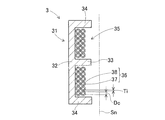
- FIG. 3 is a cross-sectional view of the feeding coil 3 when the AA cross section indicated by the alternate long and short dash line in FIG. 2 is viewed from the direction of the arrow.
- the feeding coil 3 includes a core 31 and a winding 35.
- the core 31 is an E-shaped core having an E-shaped cross section, and includes a bottom surface portion 32, a middle leg portion 33, and two side leg portions 34.
- the bottom surface portion 32 is formed in a rectangular plate shape.
- the two side leg portions 34 on which the winding 35 is not disposed stand up from the two long sides of the bottom surface portion 32 and are parallel to each other.
- the middle leg portion 33 on which the winding 35 is disposed rises from the center of the bottom surface portion 32.
- the middle leg portion 33 is parallel to the two side leg portions 34 and has a shorter moving direction than the side leg portion 34.
- the standing height dimensions of the middle leg portion 33 and the side leg portion 34 are equal to each other.
- the core 31 can be formed as an integral product by, for example, sintering magnetic powder or laminating electromagnetic steel plates.
- the winding 35 is disposed around the middle leg portion 33.
- the winding 35 is formed by winding a wire 36 around a winding mold corresponding to the shape of the middle leg portion 33.
- the wire 36 has an insulating coating 38 around the conductor 37.
- the conductor 37 is a single conductor made of a single strand having a circular cross section with a diameter of Dc, such as a copper wire or an aluminum wire.
- the conductor 37 may be a rectangle with a chamfered cross section, a composite conductor made of a plurality of strands, or a material other than copper or aluminum.
- the insulating coating 38 is made of resin or the like, and the coating thickness on one side thereof is Ti.
- the winding 35 is obtained by winding the wire 36 in parallel with the facing intermediate surface Sn when the power feeding coil 3 and the power receiving coil 4 face each other.
- the winding 35 is composed of a total of 12 turns, 6 turns for each of the two layers.
- the number of layers of the winding 35 and the number of turns per layer can be changed as appropriate. As shown in FIG. 2, both ends 351 and 352 of the winding 35 are drawn out in the short side direction of the bottom surface portion 32 of the core 31.
- the cross-sectional area of the conductor 37 in other words, the diameter Dc of the circular cross-section is determined based on the winding resistance value R.
- the winding resistance value R is obtained by adding the DC resistance value Rdc of the winding 35 and the AC resistance value Rac of the winding 35 that is an increase in resistance due to the skin effect occurring at a specific frequency.
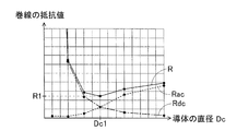
- FIG. 4 is a diagram illustrating a result of obtaining a relationship between the diameter Dc of the conductor 37 and the resistance values R, Rdc, and Rac of the winding 35 by simulation for the feeding coil 3.
- the resistance values R, Rdc, and Rac are obtained with the six types of diameters Dc while keeping the coating thickness Ti of the insulating coating 38 constant.
- the winding resistance value R is indicated by a solid line
- the DC resistance value Rdc is indicated by a one-dot chain line
- the AC resistance value Rac is indicated by a broken line.
- the diameter Dc of the conductor 37 is determined based on the diameter Dc1.
- the magnitude of the DC resistance value Rdc does not depend on the specific frequency, but the magnitude of the AC resistance value Rac depends on the specific frequency. For this reason, when the specific frequency is changed, the diameter Dc1 may change.
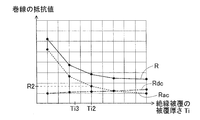
- FIG. 5 is a diagram illustrating a result of obtaining a relationship between the coating thickness Ti of the insulating coating 38 and the resistance values R, Rdc, and Rac of the winding 35 by simulation targeting the power feeding coil 3.
- the resistance values R, Rdc, and Rac are obtained with five types of coating thicknesses Ti, respectively.
- the DC resistance value Rdc is indicated by a solid line
- the DC resistance value Rdc is indicated by a one-dot chain line
- the AC resistance value Rac is indicated by a broken line.
- the DC resistance value Rdc increases with a very small slope as the coating thickness Ti increases.
- the AC resistance value Rac tends to decrease.
- the condition that the influence of the proximity effect is a predetermined amount or less can be replaced with a condition that the AC resistance value Rac is equal to or less than the predetermined resistance value R2.
- the coating thickness Ti of the insulating coating 38 is equal to or greater than the coating thickness Ti2 at which the AC resistance value Rac is equal to or less than the resistance value R2.
- the coating thickness Ti needs to be the coating thickness Ti3 that can ensure the insulation performance between the conductors 37. Therefore, the coating thickness Ti of the insulating coating 38 is determined on the larger side of the coating thickness Ti2 and the coating thickness Ti3.
- the diameter Dc of the conductor 37 of the wire rod 36 and the coating thickness Ti of the insulating coating 38 can be optimized. Thereby, in the feeding coil 3, the occurrence of AC loss due to the skin effect and the proximity effect is suppressed.
- the core 31 and the winding 35 are formed separately and are integrally coupled later. Due to the integral connection, the middle leg portion 33 of the core 31 is fitted into the hollow portion at the center of the winding 35.
- the side legs 34 of the core 31 cover a part of the outer periphery of the winding 35 that is parallel to the moving direction of the moving body 99.
- the core 31 does not cover the remaining part of the outer periphery of the winding 35 that intersects the moving direction.
- the bottom surface portion 32 of the core 31 covers the end surface portion of the winding 35 on the side away from the facing intermediate surface Sn. Therefore, in the feeding coil 3, loss due to leakage magnetic flux is reduced.
- a plurality of the feeding coils 3 are arranged in the moving direction of the moving body 99 and used. For this reason, between the feeding coils 3, most of the leakage magnetic flux goes to the adjacent feeding coil 3, and a very small part of the leakage magnetic flux leaks to the outside. That is, the necessity for magnetic shielding is small in the remaining range of the outer periphery of the winding 35. Therefore, a sufficient magnetic shielding effect can be obtained without providing side legs on the two short sides of the bottom surface portion 32. Thereby, the shape of the core 31 is simplified and the effect of weight reduction and cost reduction arises. In addition, if the side legs are provided on the two short sides of the bottom surface portion 32, when the power receiving coil 4 starts to deviate from the directly-facing positional relationship with respect to the power feeding coil 3, it is impossible to form a favorable circuit. Occurs.
- the power receiving coil 4 corresponds to an embodiment of the non-contact power feeding coil of the present invention.
- FIG. 6 is a front view of the power receiving coil 4 of the embodiment. The left-right direction in FIG. 6 corresponds to the moving direction of the moving body 99.
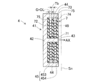
- FIG. 7 is a cross-sectional view of the power receiving coil 4 as seen from the direction of the arrow along the line BB indicated by the alternate long and short dash line in FIG.
- the power receiving coil 4 includes a core 41, a winding 45, and a bobbin 7.
- the core 41 is an E-shaped core having an E-shaped cross section, and includes a bottom surface portion 42, a middle leg portion 43, and two side leg portions 44.
- the bottom surface portion 42 is formed in a rectangular plate shape.
- the two side leg portions 44 on which the winding 45 is not disposed stand up from the two long sides of the bottom surface portion 42 and are parallel to each other.
- the middle leg portion 43 on which the winding 45 is disposed rises from the center of the bottom surface portion 42.
- the middle leg portion 43 is parallel to the two side leg portions 44 and has a shorter length in the moving direction than the side leg portion 44.
- the standing direction of the middle leg portion 43 is the direction of the axis AX perpendicular to the opposing intermediate surface Sn.
- the standing height dimensions of the middle leg portion 43 and the side leg portion 44 are equal to each other.
- the core 41 can be formed as an integral product by, for example, sintering magnetic powder or laminating electromagnetic steel plates.
- the length dimension LR of the core 41 of the power receiving coil 4 is smaller than the length dimension LS of the core 31 of the power feeding coil 3 (see FIG. 2).
- the width dimension WR of the core 41 of the power receiving coil 4 is substantially equal to the width dimension WS of the core 31 of the power feeding coil 3 (see FIG. 2). Therefore, when the feeding coil 3 and the power receiving coil 4 face each other, the middle leg portions 33 and 43 and the two side leg portions 34 and 44 face each other to form a circular magnetic path. In addition, this directly-facing positional relationship is maintained until the moving body 99 moves to some extent.
- the bobbin 7 includes a middle leg main partition 71, a bottom main partition 72, a block partition 73, and a block end partition 74.
- the middle leg main partition portion 71 is a rectangular cylindrical portion that circulates around the middle leg portion 43 of the core 41.
- the bottom main partition 72, the block partition 73, and the block end partition 74 are each an annular plate-shaped portion, and are in contact with each other around the middle leg main partition 71 and arranged in parallel to each other.
- the bottom main partition 72 is disposed in contact with the bottom 42 of the core 41.
- the block end partition portion 74 is arranged in accordance with the front end surfaces of the middle leg portion 43 and the side leg portion 44 of the core 41.
- the block partition part 73 is disposed between the bottom main partition part 72 and the block end partition part 74.
- winding accommodating spaces 75 having a gap dimension G in the axis AX direction are respectively partitioned.
- the winding accommodating space 75 is a thin ring-shaped space in the axis AX direction.
- the bobbin 7 has a robust winding function for forming the winding 45, and also has a function for ensuring insulation performance between the core 41 and the winding 45.
- the bobbin 7 can be formed as an integral product, for example, by a method such as joining a plurality of resin members or casting resin molding.
- the winding 45 includes two annular plate winding blocks 453 and 454.
- the two annular plate-like winding blocks 453 and 454 are accommodated in the winding accommodating space 75, respectively, and are arranged apart from each other in the axial direction AX.
- the ring-shaped plate winding blocks 453 and 454 are formed by winding the litz wire 49 around the axis AX in the radial direction for six turns.
- the number of winding turns of the litz wire 49 is not limited to six turns. Moreover, it may replace with the litz wire 49 and may use the wire which has insulation coating around a single conductor.
- the two annular plate winding blocks 453 and 454 are electrically connected in series, but may be connected in parallel.
- FIG. 8 is a partial cross-sectional view schematically showing the litz wire 49 and the winding housing space 75 used for the power receiving coil 4.
- the litz wire 49 is formed by twisting seven wire rods 46, and may have a wire rod configuration other than this. As indicated by the broken line, the cross-sectional shape of the litz wire 49 is equivalent to a circle, and the equivalent outer diameter is DL.
- the wire 46 has an insulating coating 48 around the conductor 47.
- the conductor 47 is a copper wire or aluminum wire having a circular cross section.
- the insulating coating 48 is made of formal resin, for example.
- the litz wire 49 can significantly reduce the influence of the skin effect as compared to a single wire having a large diameter, and has the effect of reducing the AC loss of the power receiving coil 4.
- the winding 45 is obtained by winding a litz wire 49 in parallel with the facing intermediate surface Sn when the feeding coil 3 and the receiving coil 4 face each other. As shown in FIG. 6, both ends 451 and 452 of the winding 45 are drawn out in the short side direction of the bottom surface portion 42 of the core 41.
- the gap dimension G between the two winding housing spaces 75 is set to be equal to the equivalent outer diameter dimension DL of the litz wire 49. For this reason, in the winding operation for forming the power receiving coil 4, the cross-sectional shape of the litz wire 49 is not lost. Therefore, in the power receiving coil 4, the effect of reducing the AC loss when the litz wire 49 is used becomes more prominent than when a single wire having a large diameter is used.
- FIG. 9 is a partial cross-sectional view illustrating the case where the litz wire 49X loses its shape.
- the gap dimension GX of the winding accommodating space 75X of the bobbin 7X is larger than the equivalent outer diameter dimension DL, the circular cross-sectional shape of the litz wire 49X is deformed by the force applied during the winding operation. Thereby, there exists a possibility that the reduction effect of alternating current loss when using the litz wire 49X may be impaired.
- the gap size G of the winding housing space 75 is made smaller than the equivalent outer diameter DL of the litz wire 49, the circular cross-sectional shape of the litz wire 49 loses its shape. In addition, since the litz wire 49 is inserted into the narrow winding housing space 75, the insulation coating 48 may be damaged.
- the thickness Tb of the block partition 73 is determined such that the influence of the proximity effect generated at a specific frequency between the litz wires 49 sandwiching the block partition 73 is not more than a predetermined amount.
- the influence of the proximity effect is reduced by increasing the thickness Tb.
- increasing the thickness Tb is directly linked to disadvantages such as an increase in the size, weight, and cost of the power receiving coil 4. Therefore, these disadvantages are also considered comprehensively, and the thickness Tb of the block partitioning portion 73 is set to an optimum value. Thereby, in the receiving coil 4, generation
- the winding 45 is formed by winding a litz wire 49 around a bobbin 7 serving as a winding form. Thereafter, the winding 45 and the bobbin 7 are integrally coupled to a separately formed core 41.
- the middle leg portion 43 of the core 41 is fitted into the hollow portion at the center of the winding 45 and the middle leg main partitioning portion 71 of the bobbin 7.
- the side leg portion 44 of the core 41 covers a part of the outer peripheral portion of the winding 45 that is parallel to the moving direction of the moving body 99.
- the core 41 does not cover the remaining portion of the outer periphery of the winding 45 that intersects the moving direction of the moving body 99.
- the bottom surface portion 42 of the core 41 covers the end surface portion of the winding 45 on the side away from the facing intermediate surface Sn. Therefore, the magnetic shielding effect which suppresses that the magnetic flux which arrived from the feed coil 3 leaks outside arises. Therefore, even in the power receiving coil 4, loss due to leakage magnetic flux is reduced.
- winding 45 using three or more annular plate winding blocks.
- the number of the block partitioning portions 73 and the winding accommodating spaces 75 is increased corresponding to the number of the annular plate winding blocks.
- FIG. 10 is a cross-sectional view of a power receiving coil 4A according to another embodiment.
- the power receiving coil 4A includes a core 41, a winding 45A, and a bobbin 7A.
- the core 41 shown in FIG. 10 has the same shape as the core 41 shown in FIGS. 6 and 7.
- the bobbin 7A is an integrated product including a middle leg main partition 71, a bottom main partition 72, and four block partitions 76 to 79.
- the middle leg main partition portion 71 is a rectangular cylindrical portion that circulates around the middle leg portion 43 of the core 41.
- the bottom main partition portion 72 is a ring-shaped plate-like portion, is disposed around the middle leg main partition portion 71, and contacts the bottom portion 42 of the core 41.
- the four block partition portions 76 to 79 are rectangular cylindrical portions.
- the four block partitioning portions 76 to 79 are arranged around the middle leg main partitioning portion 71 so as to be separated from each other inside and outside. One ends of the block partition portions 76 to 79 in the direction of the axis AX are connected to the bottom main partition portion 72.
- a winding accommodating space 75A is defined between the middle leg main partition 71 and the innermost block partition 76. Further, a winding accommodating space 75A is also defined between the block partition portions 76 to 79, respectively. A total of four winding housing spaces 75A are cylindrical spaces. The gap dimension G in the direction intersecting the axis AX of the winding accommodating space 75A is set equal to the equivalent outer diameter DL of the litz wire 49.
- the winding 45A is composed of four cylindrical winding blocks 455 to 458 arranged in the radial direction.
- Each of the cylindrical winding blocks 455 to 458 is housed in the winding housing space 75A.
- the cylindrical winding blocks 455 to 458 are formed by winding the litz wire 49 around the axis AX for two turns in the direction of the axis AX.
- the number of winding turns of the litz wire 49 is not limited to two turns.
- the four cylindrical winding blocks 455 to 458 are electrically connected in series, but may be connected in parallel.
- the gap dimension G of each winding accommodating space 75A is equal to the equivalent outer diameter DL of the litz wire 49, the litz wire 49 is not deformed in the winding operation. Accordingly, the power receiving coil 4A has a remarkable effect of reducing the AC loss when the litz wire 49 is used as compared with a case where a single wire having a large diameter is used. Further, the thickness Tb of the block partition portions 76 to 78 is determined so that the influence of the proximity effect generated at a specific frequency between the litz wires 49 sandwiching the block partition portions 76 to 78 becomes a predetermined amount or less. Thereby, generation
- the power receiving coil 4 corresponds to an embodiment of the non-contact power feeding coil of the present invention.
- the power receiving coil 4 includes a winding 45 through which an alternating current of a specific frequency flows, and a core 41 that forms a part of a circular magnetic path linked to the winding 45, and forms a non-contact power feeding system 1.
- the coil 45 is composed of annular plate-shaped winding blocks 453 and 454 each having a litz wire 49 formed of a plurality of wires 46 each having an insulating coating 48 around a conductor 47.
- the bobbin 7 further includes a middle leg main partition portion 71 that partitions the winding 45 and the core 41, a bottom main partition portion 72, and a block partition portion 73 that partitions the plurality of winding blocks.
- the power receiving coil 4 includes a winding 45 composed of a plurality of winding blocks each wound with a litz wire 49 and a bobbin 7 having a block partitioning portion 73 that partitions the plurality of winding blocks. For this reason, the separation distance between the litz wires 49 on both sides of the block partitioning portion 73 is increased by the thickness Tb of the block partitioning portion 73. Thereby, generation
- the power receiving coil 4A corresponds to another embodiment of the non-contact power feeding coil of the present invention.
- the power receiving coil 4 ⁇ / b> A includes a winding 45 ⁇ / b> A through which an alternating current of a specific frequency flows and a core 41 that forms a part of a circular magnetic path interlinking with the winding 45 ⁇ / b> A.
- a middle leg main body that partitions a gap between the winding 45A and the core 41, and includes a plurality of cylindrical winding blocks 455 to 458 each wound with a litz wire 49 composed of a plurality of wires 46 each having an insulating coating 48.
- a bobbin 7A having a partition portion 71, a bottom main partition portion 72, and block partition portions 76 to 78 for partitioning a plurality of winding blocks is further provided.
- the separation distance between the litz wires 49 sandwiching the block partition portions 76 to 78 is increased by the thickness Tb of the block partition portions 76 to 78. Thereby, generation
- the plurality of winding blocks of the power receiving coil 4 are a plurality of ring-shaped plate winding blocks 453 and 454 formed by winding the litz wire 49 in order in the radial direction and arranged in the axis AX direction.
- the plurality of winding blocks of the power receiving coil 4A are a plurality of cylindrical winding blocks 455 to 458 that are formed by sequentially winding litz wires 49 in the direction of the axis AX and are arranged in the radial direction. According to this, the internal configuration including the winding method of the windings 45 and 45A can be changed according to the power receiving capacity required for the power receiving coils 4 and 4A, the difficulty level of the winding work, etc. Great freedom.
- the thickness Tb of the block partition portions 73 and 76 to 78 of the power receiving coils 4 and 4A is affected by the proximity effect generated at a specific frequency between the litz wires 49 sandwiching the block partition portions 73 and 76 to 78 by a predetermined amount. It was determined to be as follows. According to this, not only the influence of the proximity effect but also the disadvantages such as an increase in the size of the power receiving coils 4 and 4A, an increase in weight, and a cost increase are comprehensively considered, and the thickness Tb of the block partitioning portion 73 is an optimum value. Can be determined. Therefore, the occurrence of AC loss due to the proximity effect is appropriately suppressed.
- the plurality of winding blocks of the power receiving coils 4 and 4A are formed by winding litz wires 49 each formed by twisting a plurality of wires 46.
- the clearance dimension G between the bottom face main partition part 72 and the block partition part 73 of the bobbin 7 around which the litz wire 49 is wound, the clearance dimension G between the block partition part 73 and the block end partition part 74, and The gap dimension G between the middle leg main partition 71 and the block partition 76 in the bobbin 7A and the gap dimension G between the block partitions 76 to 79 are equal to the equivalent outer diameter DL of the litz wire 49. According to this, since the cross-sectional shape of the litz wire 49 does not lose its shape, the effect of reducing the AC loss due to the skin effect becomes significant.
- the winding 45 of the power receiving coil 4 is formed by winding the litz wire 49 in parallel with the opposing intermediate surface Sn and sequentially in the radial direction, and the axis AX orthogonal to the opposing intermediate surface Sn.
- the core 41 is composed of a plurality of annular plate-like winding blocks 453 and 454 arranged in the direction, and the core 41 covers at least a part of the outer periphery of the winding 45 and the middle leg portion 43 fitted in the hollow portion at the center of the winding 45.
- the side leg portion 44 and the bottom surface portion 42 covering the end surface portion on the side away from the facing intermediate surface of the winding 45 are provided, and the block partitioning portion 73 of the bobbin 7 has an annular plate shape. According to this, the magnetic shielding effect which suppresses that the magnetic flux which arrived from the feed coil 3 leaks outside arises. Therefore, even in the power receiving coil 4, loss due to leakage magnetic flux is reduced.
- the contactless power supply system 1 of the embodiment is provided in a power supply coil 3 provided in the power supply unit 1S, an AC power supply circuit 2 that supplies AC power of a specific frequency to the power supply coil 3, and a power reception unit 1R.
- a power receiving coil that is electrically coupled to face the coil 3 and receives AC power in a non-contact manner, and a power receiving circuit 5 that converts the AC power received by the power receiving coil to generate a drive voltage and outputs the drive voltage to the electrical load.
- the power feeding coil 3 includes a winding 35 through which an alternating current of a specific frequency flows, and a core 31 that forms a part of a circular magnetic path interlinked with the winding 35.
- the winding 35 is obtained by winding a wire 36 having an insulation coating 38 around a conductor 37.
- the coating thickness Ti of the insulation coating 38 is a proximity generated at a specific frequency between the adjacent wires 36. Effect shadow There is determined to be equal to or less than a predetermined amount, the power receiving coil is a receiving coil 4 or the power receiving coil 4A described above.
- the coating thickness Ti of the insulating coating 38 of the wire 36 of the power feeding coil 3 not only ensures the insulating performance between the conductors 37 but also the influence of the proximity effect is less than a predetermined amount. It is determined to be. For this reason, the separation distance between the conductors 37 can be freely adjusted by changing the coating thickness Ti, and the occurrence of AC loss due to the proximity effect is appropriately suppressed.
- the power receiving coil is the power receiving coil 4 or the power receiving coil 4A described above, and the occurrence of AC loss is suppressed. Therefore, the AC loss is reduced in both the power feeding coil 3 and the power receiving coils 4 and 4A, and in the non-contact power feeding system 1, good power feeding efficiency is obtained.
- the same number of power feeding units 1S are provided in each of the plurality of first to third board production machines 91 to 93 that constitute the board production line 9, and the power receiving unit 1R includes: A plurality of first to third substrate production machines 91 to 93 are provided on a moving body 99 that moves in the direction in which they are arranged.
- the contactless power supply coil of the present invention can be used for system configurations other than the contactless power supply system 1 of the embodiment. Further, the contactless power supply system 1 of the embodiment is not limited to application to the board production line 9, but can be applied to a wide range of fields such as assembly lines and processing lines for producing other products, power supply during traveling of electric vehicles, and the like. .
Landscapes
- Engineering & Computer Science (AREA)
- Power Engineering (AREA)
- Transportation (AREA)
- Mechanical Engineering (AREA)
- Computer Networks & Wireless Communication (AREA)
- Physics & Mathematics (AREA)
- Electromagnetism (AREA)
- Manufacturing & Machinery (AREA)
- Microelectronics & Electronic Packaging (AREA)
- Current-Collector Devices For Electrically Propelled Vehicles (AREA)
- Insulating Of Coils (AREA)
- Coils Of Transformers For General Uses (AREA)
Abstract
本発明の非接触給電用コイルは、特定周波数の交流電流が流れる巻線(45)と、巻線に鎖交する周回磁路の一部を形成するコア(41)とを備え、非接触給電システム(1)を構成する受電コイル(4)であって、巻線は、導体(47)の周りに絶縁被覆(48)を有する線材(46)がそれぞれ巻回された複数の巻線ブロック(453、454)からなり、巻線とコアとの間を仕切る主仕切り部(71、72)、および、複数の巻線ブロックの相互間を仕切るブロック間仕切り部(73)をもつボビン(7)をさらに備えた。これによれば、ブロック間仕切り部を挟んだ両側の線材の導体間の離隔距離がブロック間仕切り部の厚さ(Tb)分だけ大きくなり、近接効果に起因する交流損失の発生が抑制される。
Description
本発明は、巻線とコアとを備える非接触給電用コイル、および、この非接触給電用コイルを用いて構成する非接触給電システムに関する。
多数の部品が実装された基板を生産する基板生産機として、はんだ印刷機、電子部品装着機、リフロー機、基板検査機などがある。これらの設備を連結して基板生産ラインを構成することが一般的になっている。さらに、モジュール化された同じ大きさの基板生産機を列設して基板生産ラインを構成する場合も多い。モジュール化された基板生産機を用いることにより、ラインの組み替え時やラインを長大化する増設時の段取り替え作業が容易になり、フレキシブルな基板生産ラインが実現される。
近年、基板生産ラインの各基板生産機で使用する機材や部材を、基板生産ラインに沿って移動する移動体に搬送させ、省力化および自動化を推進することが検討されている。さらに、移動体への給電手段として、非接触給電システムが考えられている。なお、非接触給電システムの用途は、基板生産ラインに限定されず、他の製品を生産する組立ラインや加工ライン、電動車両の走行中給電など幅広い分野にわたっている。この種の非接触給電システムでは、給電素子および受電素子にそれぞれコイルを用いる電磁結合方式が多用される。電磁結合方式の非接触給電システムに関する技術例が、特許文献1に開示されている。なお、本明細書の中で、電磁結合方式は、電磁誘導方式および電磁界共鳴方式を含むものである。
特許文献1の非接触電力伝送装置は、送電部(給電ユニット)および受電部(受電ユニット)にそれぞれコイルを備え、各コイルを通じで交流電力の送電および受電を行い、受電した交流電力を直流電力に変換して負荷に供給する。特許文献1に限らず電磁結合方式の非接触給電システムでは、一般的に、商用周波数よりも格段に高い周波数を用いることによって、空間を介した給電を可能としている。しかしながら、周波数が高いことで巻線の交流損失や漏洩磁束による損失が増加し、給電効率が低下しがちであった。
交流損失は、巻線内の渦電流によって発生するものであり、周波数が高いほど増加する。交流損失として、1本の導体内で発生する表皮効果に起因するもの、および複数の導体の相互間に発生する近接効果に起因するものが有る。また、漏洩磁束が到達する周辺の金属物では電流が流れて発熱するため、損失の増加を招く。損失の増加を抑制する非接触給電用コイルの各種技術例が特許文献2~4に開示されている。
特許文献2は、非接触電力伝送機器の送電用コイル(給電コイル)または受電用コイル(受電コイル)に用いられる渦巻状の電線部から成る平面コイルを開示している。この平面コイルは、電線部間に渦電流抑制用の隙間を設けたことを特徴とする。これによれば、隣接する電線部同士が互いに影響を及ぼし合って渦電流を発生することが抑制され(近接効果の抑制)、平面コイルの発熱が低減される、とされている。
特許文献3は、電源と、給電側共鳴コイルと、該コイルを収容する導電性の遮蔽ケースと、を備えた給電部を開示している。この給電部は、遮蔽ケースの外部に配置された磁性体をさらに備える。これによれば、給電側共鳴コイルにより発せられた磁界のうち遮蔽ケースから漏れた漏洩磁界が磁性体(フェライト)により吸収されるため、十分に電磁漏洩を防止できる、とされている。
特許文献4は、H字状のコアを有して電線が巻回されたコイル本体と、該コイル本体を収容する樹脂製のケース本体と、ケース本体が固定された磁気遮蔽用の非磁性導電体板と、を備える非接触給電用コイル装置を開示している。この非接触給電用コイル装置は、非磁性導電体板の裏面に、共振コンデンサおよび整流回路を収容した筺体を配置している。さらに、実施形態には、損失を低減する一方策として、リッツ線が開示されている。これによれば、短い配線でコンパクトに装置を構成でき、磁気遮蔽効果を損なわずに、給電効率の低下が抑えられる、とされている。
ところで、特許文献2の実施形態に説明された平面コイルの製造方法では、電線部間の隙間を確保するために、専用の布線装置を用いて電線部をシート上に布線してゆく。他に、電線部間にスペーサを挿入しながらコイルを形成する巻回作業を行ってゆく方法も考えられる。しかしながら、これらの工夫をしても、平面コイルの製造は容易でなく、寸法精度の低下による交流損失の増加や、製造に要する作業工数の増加などの点に難が有ると考えられる。
また、特許文献3の技術例では、磁性体の外側への電磁漏洩は防止できても、磁性体の内側の遮蔽ケースに漏洩磁束が入り込む。したがって、遮蔽ケースに渦電流損が発生して損失が増加する。また、特許文献4に開示されたリッツ線は、単一の導体からなる線材と比較して高価であるが、表皮効果に起因する交流損失を顕著に低減できる。しかしながら、巻回作業の際にリッツ線の断面形状が型崩れして、交流損失低減の効果が損なわれてしまうおそれがある。
上記したように給電コイルや受電コイルの損失が増加すると、当然ながら非接触給電システムの給電効率は低下する。
本発明は、上記背景技術の問題点に鑑みてなされたものであり、交流損失の発生を抑制した非接触給電用コイルを提供すること、および、この非接触給電用コイルを用いることで良好な給電効率が得られる非接触給電システムを提供することを解決すべき課題とする。
上記課題を解決する本発明の非接触給電用コイルは、特定周波数の交流電流が流れる巻線と、前記巻線に鎖交する周回磁路の一部を形成するコアとを備え、非接触給電システムを構成する給電コイルおよび受電コイルの少なくとも一方に用いられる非接触給電用コイルであって、前記巻線は、導体の周りに絶縁被覆を有する線材がそれぞれ巻回された複数の巻線ブロックからなり、前記巻線と前記コアとの間を仕切る主仕切り部、および、前記複数の巻線ブロックの相互間を仕切るブロック間仕切り部をもつボビンをさらに備えた。
また、本発明の非接触給電システムは、給電ユニットに設けられた給電コイルと、前記給電コイルに前記特定周波数の交流電力を供給する交流電源と、受電ユニットに設けられ、前記給電コイルに対向すると電気的に結合して非接触で交流電力を受け取る受電コイルと、前記受電コイルが受け取った交流電力を変換して駆動電圧を生成し、電気負荷に出力する受電回路と、を備えた非接触給電システムであって、前記給電コイルは、特定周波数の交流電流が流れる巻線と、前記巻線に鎖交する周回磁路の一部を形成するコアとを有し、前記巻線は、導体の周りに絶縁被覆を有する線材が巻回されたものであり、前記絶縁被覆の被覆厚さは、隣接する前記線材の相互間に前記特定周波数で生じる近接効果の影響が所定量以下となるように定められ、前記受電コイルは、上記した本発明の非接触給電用コイルである。
本発明の非接触給電用コイルにおいて、近接効果に起因する交流損失の発生が抑制される。
本発明の非接触給電システムにおいて、良好な給電効率が得られる。
(1.実施形態の非接触給電システム1の全体構成)
まず、本発明の実施形態の非接触給電システム1について、図1を参考にして説明する。図1は、実施形態の非接触給電システム1の全体構成を模式的に説明する図である。実施形態の非接触給電システム1は、基板生産ライン9に適用される。図示されるように、基板生産ライン9は、3台の第1~第3基板生産機91~93が列設されて構成されている。図1の左右方向は、第1~第3基板生産機91~93の列設方向であり、後述する移動体99の移動方向でもある。
まず、本発明の実施形態の非接触給電システム1について、図1を参考にして説明する。図1は、実施形態の非接触給電システム1の全体構成を模式的に説明する図である。実施形態の非接触給電システム1は、基板生産ライン9に適用される。図示されるように、基板生産ライン9は、3台の第1~第3基板生産機91~93が列設されて構成されている。図1の左右方向は、第1~第3基板生産機91~93の列設方向であり、後述する移動体99の移動方向でもある。
各基板生産機91~93は、モジュール化されており、列設方向の幅寸法MLが互いに等しい。第1~第3基板生産機91~93は列設位置の順序変更、およびモジュール化された他の基板生産機との入れ替えが可能とされている。基板生産ライン9を構成する基板生産機の列設台数は4台以上でもよく、後から列設台数を増やすモジュール増設対応も可能になっている。換言すると、基板生産機の順序変更時や増設時に、非接触で給電を行うためにケーブル等の配線を行うことなく、移動体99は、列設された基板生産機に沿って移動可能になる。第1~第3基板生産機91~93として、電子部品装着機を例示でき、これに限定されない。
第1~第3基板生産機91~93の前方には、列設方向に延在する図略のガイドレールが配設されている。移動体99は、ガイドレールに沿って移動方向(第1~第3基板生産機91~93の列設方向)に移動する。移動体99は、各基板生産機91~93で使用する機材や部材を図略の保管庫から搬入し、使用後の機材や部材を保管庫に戻す役割を担っている。
実施形態の非接触給電システム1は、移動体99を給電対象として、第1~第3基板生産機91~93から電磁結合方式で非接触給電を行うシステムである。非接触給電システム1は、各基板生産機91~93の前側にそれぞれ設けられた給電ユニット1S、および、移動体99に設けられた2組の受電ユニット1Rから構成されている。
給電ユニット1Sは、交流電源回路2および給電コイル3などで構成される。交流電源回路2は、給電コイル3に特定周波数の交流電力を供給する。交流電源回路2は、例えば、直流電圧を供給する直流電源部と、直流電圧を交流変換する公知のブリッジ回路とを用いて構成できる。交流電源回路2の第1出力端子21は、給電コイル3の一端に直結されており、第2出力端子22は、給電側コンデンサ61の一端に接続されている。交流電源回路2の特定周波数は、後述する給電側共振回路および受電側共振回路の共振周波数に基づいて設定される。特定周波数として、数10kHz~数100kHzのオーダーを例示でき、これに限定されない。交流電源回路2は、電圧値などを調整する機能を具備していてもよい。
3台の基板生産機91~93に設けられた合計3個の交流電源回路2は、相互に独立して動作可能となっている。各基板生産機91~93は、移動体99の接近を検出する図略のセンサを有している。そして、各基板生産機91~93の交流電源回路2は、移動体99が接近したときだけ動作する。これにより、移動体99が遠方に離隔している間、交流電源回路2は停止され、無駄な電気損失が発生しない。
給電コイル3は、各基板生産機91~93の前面に設けられており、搬送方向の前後で対称形状に形成されている。給電側コンデンサ61は、給電コイル3に直列接続されて給電側共振回路を形成する共振用素子である。給電側コンデンサ61の他端は、給電コイル3の他端に接続されている。これにより、環状の給電回路が構成される。したがって、給電コイル3には、特定周波数の交流電流が流れる。
一方、受電ユニット1Sは、受電コイル4および受電回路5などで構成される。2個の受電コイル4は、移動体99の給電コイル3に対向する側面98に配設されており、移動方向に沿い相互に離間して配置される。給電コイル3および受電コイル4は、対向中間面Snを挟んで配置されると、後述するコア31、41同士が共同で周回磁路を形成して電磁結合する。これにより、給電コイル3と受電コイル4との間に相互インダクタンスが発生して非接触給電が可能になる。したがって、受電コイル4にも、特定周波数の交流電流が流れる。給電コイル3と受電コイル4との実際の離間距離は、図示された離間距離よりも小さい。
受電コイル4の一端は、受電側コンデンサ65の一端、および受電回路5を構成する整流回路51の入力側の一端子に接続されている。受電コイル4の他端は、受電側コンデンサ65の他端、および整流回路51の入力側の他端子に接続されている。受電側コンデンサ65は、受電コイル4に並列接続されて受電側共振回路を形成する共振用素子である。
受電回路5は、受電コイル4が受け取った交流電力を変換して駆動電圧を生成する。受電回路5は、受電コイル4ごとに設けられた整流回路51、および2個の整流回路51に対して共通に設けられた直流電源回路55を含んで構成される。整流回路51は、例えば、4個の整流ダイオードをブリッジ接続した全波整流回路、および全波整流回路の出力側に接続された平滑コンデンサによって構成される。2個の整流回路51は、受電コイル4が受け取った交流電力を直流電圧に変換して出力する。2個の整流回路51の出力側は、直流電源回路55に並列接続されている。
直流電源回路55は、直流電圧を駆動電圧に変換して、移動体99に搭載された電気負荷ELに出力する。直流電源回路55は、駆動電圧の安定化作用を有する。つまり、直流電源回路55は、整流回路51から出力された電圧値不定の直流電圧を概ね一定の駆動電圧に調整して、電気負荷ELに給電する。直流電源回路55として、スイッチング方式またはドロッパ方式のDCDCコンバータを例示できる。直流電源回路55は、降圧機能を具備しており、さらに昇圧機能を具備していてもよい。
電気負荷ELは、移動体99上で仕事を行うものであり、その種類や消費電力などは限定されない。電気負荷ELは、移動体99の移動用駆動源、例えばステッピングモータやサーボモータなどを含んでいてもよい。
ここで、給電コイル3および受電コイル4の移動方向の長さ、および移動方向に隣り合う相互離間距離は、非接触給電が安定して行われるように設定されている。つまり、移動体99の位置に関係なく常に、給電コイル3と少なくとも1個の受電コイル4とが正対状態になる。正対状態とは、給電コイル3の移動方向の長さの範囲内に、受電コイル4の移動方向の長さの全体が対向する状態を意味する。
図1に例示される位置関係において、第1基板生産機91の給電コイル3と図中の左側の受電コイル4とが正対し、第2基板生産機92の給電コイル3と図中の右側の受電コイル4とが正対している。このとき、2個の受電コイル4は、ともに良好な受電状態となり、矢印P1、P2に示されるように大きな交流電力を受け取ることができる。正対状態にある受電コイル4は、単独でも電気負荷ELを駆動できるだけの受電容量を有する。したがって、非接触給電システム1は、バッテリおよび充電回路を必要としない。
(2.実施形態の給電コイル3の詳細な構成)
次に、実施形態の給電コイル3の詳細な構成について説明する。図2は、実施形態の給電コイル3の正面図である。図2の左右方向は、移動体99の移動方向に対応する。図3は、図2に一点鎖線で示されたA-A断面を矢視方向から見た給電コイル3の断面図である。給電コイル3は、コア31および巻線35を備える。
次に、実施形態の給電コイル3の詳細な構成について説明する。図2は、実施形態の給電コイル3の正面図である。図2の左右方向は、移動体99の移動方向に対応する。図3は、図2に一点鎖線で示されたA-A断面を矢視方向から見た給電コイル3の断面図である。給電コイル3は、コア31および巻線35を備える。
図3に示されるように、コア31は、断面がE字形状のE形コアであり、底面部32、中脚部33、および2つの側脚部34からなる。底面部32は、長方形板状に形成されている。巻線35が配設されない2つの側脚部34は、底面部32の2つの長辺から起立しており、相互に平行している。巻線35が配設される中脚部33は、底面部32の中央から起立している。中脚部33は、2つの側脚部34に平行しており、かつ、移動方向の長さが側脚部34よりも短い。中脚部33および側脚部34の起立した高さ寸法は、相互に等しい。コア31は、例えば、磁性粉体を焼結し、または電磁鋼板を積層して、一体品に形成することができる。
巻線35は、中脚部33の周りに配置される。巻線35は、中脚部33の形状に相当する巻き型に線材36が巻回されて形成される。線材36は、導体37の周りに絶縁被覆38を有する。導体37は、直径がDcの円形断面の1本の素線からなる単一導体であり、銅線やアルミ線などとされる。これに限定されず、導体37は、断面が面取りされた矩形などでもよく、また、複数本の素線からなる複合導体でもよく、銅やアルミ以外の材質でもよい。絶縁被覆38は、樹脂などとされ、その片側の被覆厚さはTiである。
巻線35は、給電コイル3と受電コイル4とが対向したときの対向中間面Snに対して、線材36が平行に巻回されたものとなる。本実施形態において、巻線35は、2層各6ターンの合計12ターンで構成されている。巻線35の層数、および1層当たりのターン数は適宜変更できる。図2に示されるように、巻線35の両端351、352は、コア31の底面部32の短辺方向に引き出されている。
ここで、導体37の断面積、換言すると円形断面の直径Dcは、巻線抵抗値Rに基づいて定められている。巻線抵抗値Rは、巻線35の直流抵抗値Rdcと、特定周波数で生じる表皮効果に起因する抵抗増加分である巻線35の交流抵抗値Racとを加算して求められる。図4は、給電コイル3を対象としたシミュレーションにより、導体37の直径Dcと、巻線35の抵抗値R、Rdc、Racとの関係を求めた結果を示す図である。シミュレーションでは、絶縁被覆38の被覆厚さTiを一定に保ちつつ、6種類の直径Dcでそれぞれ抵抗値R、Rdc、Racを求めている。図4において、巻線抵抗値Rは実線、直流抵抗値Rdcは一点鎖線、交流抵抗値Racは破線でそれぞれ示されている。
図示されるように、直径Dcの増加に伴い、直流抵抗値Rdcは、直径Dcの二乗に反比例して減少する。一方、直径Dcの増加に伴って表皮効果の影響が顕著となるため、交流抵抗値Racは増加傾向を示す。そして、直流抵抗値Rdcと交流抵抗値Racとを加算した巻線抵抗値Rは、直径Dc1で可及的に小さな値R1となる。つまり、導体37の直径Dcを直径Dc1より小さくしても大きくしても、給電コイル3の損失に不利となる。このため、導体37の直径Dcは、直径Dc1に基づいて定められる。導体37の材質や断面形状、断面積(円形断面の場合直径Dc)を定めるその他の要因として、巻回作業時の作業性や、故障電流が流れたときの機械的強度なども考慮され得る。
なお、直流抵抗値Rdcの大きさは、特定周波数に依存しないが、交流抵抗値Racの大きさは、特定周波数に依存する。このため、特定周波数が変更されると、直径Dc1は変化し得る。
また、絶縁被覆38の被覆厚さTiは、隣接する線材36の相互間に特定周波数で生じる近接効果の影響が所定量以下となるように定められている。図5は、給電コイル3を対象としたシミュレーションにより、絶縁被覆38の被覆厚さTiと、巻線35の抵抗値R、Rdc、Racとの関係を求めた結果を示す図である。シミュレーションでは、導体37の直径Dcを一定に保ちつつ、5種類の被覆厚さTiでそれぞれ抵抗値R、Rdc、Racを求めている。図5において、直流抵抗値Rdcは実線、直流抵抗値Rdcは一点鎖線、交流抵抗値Racは破線でそれぞれ示されている。
図示されるように、被覆厚さTiの増加に伴い、直流抵抗値Rdcは、ごく小さな傾きで増加する。一方、被覆厚さTiの増加に伴って近接効果の影響が低減されるため、交流抵抗値Racは減少傾向を示す。ここで、近接効果の影響が所定量以下となる条件は、交流抵抗値Racが所定の抵抗値R2と以下となる条件に置き換え可能である。これによれば、絶縁被覆38の被覆厚さTiは、交流抵抗値Racが抵抗値R2以下となる被覆厚さTi2以上となる。また、一般的に、被覆厚さTiは、導体37間の絶縁性能を確保できる被覆厚さTi3とする必要が有る。したがって、絶縁被覆38の被覆厚さTiは、被覆厚さTi2および被覆厚さTi3のうち大きい側に定められる。
図4および図5を用いて説明した2種類のシミュレーションを組み合わせて実施することにより、線材36の導体37の直径Dcおよび絶縁被覆38の被覆厚さTiを最適化できる。これにより、給電コイル3では、表皮効果および近接効果に起因する交流損失の発生が抑制される。
給電コイル3の製造工程において、コア31および巻線35は別々に形成され、後で一体的に結合される。一体的な結合により、コア31の中脚部33は、巻線35の中央の中空部に嵌入する。コア31の側脚部34は、巻線35の外周部のうち移動体99の移動方向に平行する一部範囲を覆う。コア31は、巻線35の外周部のうち移動方向に交差する残部範囲を覆わない。コア31の底面部32は、巻線35の対向中間面Snから離れた側の端面部を覆う。これにより、給電コイル3から出る磁束が外部へ漏出することを抑制する磁気遮蔽効果が生じる。したがって、給電コイル3では、漏洩磁束による損失が低減される。
また、図1に示されるように、給電コイル3は、複数個が移動体99の移動方向に並べられて用いられる。このため、給電コイル3の相互間において、漏洩磁束の大部分は隣の給電コイル3に向かい、漏洩磁束のごく少ない一部が外部に漏洩する。つまり、巻線35の外周部のうち残部範囲では、磁気遮蔽の必要性が小さい。したがって、底面部32の2つの短辺に側脚部を設けずとも、十分な磁気遮蔽効果が得られる。これにより、コア31の形状が簡素化され、軽量化およびコスト低減の効果が生じる。なお、仮に底面部32の2つの短辺に側脚部を設けると、給電コイル3に対して受電コイル4が正対位置関係からずれ始めたときに、良好な周回磁路を形成できなくなる欠点が生じる。
(3.実施形態の受電コイル4の詳細な構成)
次に、実施形態の受電コイル4の詳細な構成について説明する。受電コイル4は、本発明の非接触給電用コイルの一実施形態に相当する。図6は、実施形態の受電コイル4の正面図である。図6の左右方向は、移動体99の移動方向に対応する。図7は、図6に一点鎖線で示されたB-B断面を矢視方向から見た受電コイル4の断面図である。受電コイル4は、コア41、巻線45、およびボビン7を備える。
次に、実施形態の受電コイル4の詳細な構成について説明する。受電コイル4は、本発明の非接触給電用コイルの一実施形態に相当する。図6は、実施形態の受電コイル4の正面図である。図6の左右方向は、移動体99の移動方向に対応する。図7は、図6に一点鎖線で示されたB-B断面を矢視方向から見た受電コイル4の断面図である。受電コイル4は、コア41、巻線45、およびボビン7を備える。
図7に示されるように、コア41は、断面がE字形状のE形コアであり、底面部42、中脚部43、および2つの側脚部44からなる。底面部42は、長方形板状に形成されている。巻線45が配設されない2つの側脚部44は、底面部42の2つの長辺から起立しており、相互に平行している。巻線45が配設される中脚部43は、底面部42の中央から起立している。中脚部43は、2つの側脚部44に対して平行しており、かつ、移動方向の長さが側脚部44よりも短い。中脚部43の起立方向は、対向中間面Snに垂直な軸線AX方向となる。中脚部43および側脚部44の起立した高さ寸法は、相互に等しい。コア41は、例えば、磁性粉体を焼結し、または電磁鋼板を積層して、一体品に形成することができる。
移動体99の移動方向に関して、受電コイル4のコア41の長さ寸法LRは、給電コイル3のコア31の長さ寸法LS(図2参照)よりも小さい。一方、受電コイル4のコア41の幅寸法WRは、給電コイル3のコア31の幅寸法WS(図2参照)とほぼ等しい。したがって、給電コイル3と受電コイル4とが正対すると、中脚部33、43同士、および2つの側脚部34、44同士が対向して、周回磁路が形成される。また、この正対位置関係は、移動体99がある程度移動するまで維持される。
図7に示されるように、ボビン7は、中脚主仕切り部71、底面主仕切り部72、ブロック間仕切り部73、およびブロック端仕切り部74からなる。中脚主仕切り部71は、コア41の中脚部43を周回する矩形筒状の部位である。底面主仕切り部72、ブロック間仕切り部73、およびブロック端仕切り部74は、それぞれ環形板状の部位であり、中脚主仕切り部71の周りに接して、相互に平行配置される。底面主仕切り部72は、コア41の底面部42に接して配置される。ブロック端仕切り部74は、コア41の中脚部43および側脚部44の先端面に合わせて配置される。ブロック間仕切り部73は、底面主仕切り部72とブロック端仕切り部74との中間に配置される。
底面主仕切り部72とブロック間仕切り部73との間、および、ブロック間仕切り部73とブロック端仕切り部74との間に、軸線AX方向の隙間寸法がGとなる巻線収容スペース75がそれぞれ区画される。巻線収容スペース75は、軸線AX方向に薄い環形の空間となっている。ボビン7は、巻線45を巻回形成する堅牢な巻き型の機能を有するとともに、コア41と巻線45との間の絶縁性能を確保する機能を有する。ボビン7は、例えば、複数の樹脂部材の接合や注型樹脂成型などの方法によって、一体品に形成することができる。
図7に示されるように、巻線45は、2個の環形板状巻線ブロック453、454からなる。2個の環形板状巻線ブロック453、454は、それぞれ巻線収容スペース75に収容され、軸線方向AXに離隔して並んでいる。環形板状巻線ブロック453、454は、軸線AX周りにリッツ線49が径方向に6ターンだけ巻回されて形成される。なお、リッツ線49の巻回ターン数は、6ターンに限定されない。また、リッツ線49に代えて、単一導体の周りに絶縁被覆を有する線材を用いてもよい。本実施形態において、2個の環形板状巻線ブロック453、454は、電気的に直列接続されているが、並列接続されていてもよい。
図8は、受電コイル4に用いられるリッツ線49および巻線収容スペース75を模式的に示した部分断面図である。リッツ線49は、7本の線材46が撚り合わされて構成されており、これ以外の線材構成であってもよい。破線で示されるように、リッツ線49の断面形状は等価的に円形となり、等価外径寸法はDLである。線材46は、導体47の周りに絶縁被覆48を有する。導体47は、円形断面を有する銅線やアルミ線などとされる。絶縁被覆48は、例えばホルマール樹脂とされる。リッツ線49は、太径の単一の線材と比較して表皮効果の影響を顕著に低減でき、受電コイル4の交流損失を低減する効果を有する。
巻線45は、給電コイル3と受電コイル4とが対向したときの対向中間面Snに対して、リッツ線49が平行に巻回されたものとなる。図6に示されるように、巻線45の両端451、452は、コア41の底面部42の短辺方向に引き出されている。
ここで、2個の巻線収容スペース75の隙間寸法Gは、リッツ線49の等価外径寸法DLと等しくなるように設定されている。このため、受電コイル4を形成する巻回作業において、リッツ線49の断面形状は、型崩れしない。したがって、受電コイル4では、太径の単一の線材を用いる場合と比較して、リッツ線49を用いたときの交流損失の低減効果が顕著となる。
仮に、巻線収容スペース75の隙間寸法Gをリッツ線49の等価外径寸法DLよりも大きくした場合、図9に示される状態となる。図9は、リッツ線49Xが型崩れする場合を例示説明した部分断面図である。ボビン7Xの巻線収容スペース75Xの隙間寸法GXが等価外径寸法DLよりも大きい場合、リッツ線49Xは、巻回作業時に加えられる力によって円形の断面形状が型崩れする。これにより、リッツ線49Xを用いたときの交流損失の低減効果が損なわれてしまうおそれが生じる。
また仮に、巻線収容スペース75の隙間寸法Gをリッツ線49の等価外径寸法DLよりも小さくしても、リッツ線49の円形の断面形状が型崩れする。加えて、狭隘な巻線収容スペース75に無理をしてリッツ線49を挿入することになるので、絶縁被覆48を損傷するおそれが生じる。
また、ブロック間仕切り部73の厚さTbは、ブロック間仕切り部73を挟むリッツ線49の相互間に特定周波数で生じる近接効果の影響が所定量以下となるように定められている。近接効果の影響は、厚さTbを大きくすることによって低減される。しかしながら、厚さTbを大きくすることは、受電コイル4の大型化、重量増加、およびコストアップなどの短所に直結する。したがって、これらの短所も総合的に勘案され、ブロック間仕切り部73の厚さTbは、最適値に定められる。これにより、受電コイル4では、近接効果に起因する交流損失の発生が適正に抑制される。
受電コイル4の製造工程において、巻線45は、巻き型となるボビン7にリッツ線49が巻回されて形成される。その後、巻線45およびボビン7は、別途形成されたコア41に一体的に結合される。一体的な結合により、コア41の中脚部43は、巻線45の中央の中空部、およびボビン7の中脚主仕切り部71に嵌入する。コア41の側脚部44は、巻線45の外周部のうち移動体99の移動方向に平行する一部範囲を覆う。コア41は、巻線45の外周部のうち移動体99の移動方向に交差する残部範囲を覆わない。コア41の底面部42は、巻線45の対向中間面Snから離れた側の端面部を覆う。これにより、給電コイル3から到来した磁束が外部へ漏出することを抑制する磁気遮蔽効果が生じる。したがって、受電コイル4でも、漏洩磁束による損失が低減される。
なお3個以上の環形板状巻線ブロックを用いて巻線45を構成することも可能である。この場合、環形板状巻線ブロックの個数に対応して、ブロック間仕切り部73および巻線収容スペース75の個数を増加させる。
(4.別の実施形態の受電コイル4Aの詳細な構成)
次に、別の実施形態の受電コイル4Aの詳細な構成について、説明済みの受電コイル4と異なる点を主に説明する。受電コイル4Aは、本発明の非接触給電用コイルの別の実施形態に相当する。図10は、別の実施形態の受電コイル4Aの断面図である。受電コイル4Aは、コア41、巻線45A、およびボビン7Aを備える。図10に示されるコア41は、図6および図7に示されたコア41と同一形状である。
次に、別の実施形態の受電コイル4Aの詳細な構成について、説明済みの受電コイル4と異なる点を主に説明する。受電コイル4Aは、本発明の非接触給電用コイルの別の実施形態に相当する。図10は、別の実施形態の受電コイル4Aの断面図である。受電コイル4Aは、コア41、巻線45A、およびボビン7Aを備える。図10に示されるコア41は、図6および図7に示されたコア41と同一形状である。
ボビン7Aは、中脚主仕切り部71、底面主仕切り部72、および4個のブロック間仕切り部76~79からなる一体品である。中脚主仕切り部71は、コア41の中脚部43を周回する矩形筒状の部位である。底面主仕切り部72は、環形板状の部位であり、中脚主仕切り部71の周りに配置されて、コア41の底面部42に接する。4個のブロック間仕切り部76~79は、矩形筒状の部位である。4個のブロック間仕切り部76~79は、中脚主仕切り部71の周りに、内外に相互に離隔して配置される。ブロック間仕切り部76~79の軸線AX方向の一端は、底面主仕切り部72につながっている。
中脚主仕切り部71と、最も内側のブロック間仕切り部76との間に、巻線収容スペース75Aが区画される。さらに、ブロック間仕切り部76~79の相互間にも、それぞれ巻線収容スペース75Aが区画される。合計で4箇所の巻線収容スペース75Aは、筒形状の空間となっている。巻線収容スペース75Aの軸線AXと交差する方向の隙間寸法Gは、リッツ線49の等価外径寸法DLに等しく設定されている。
図10に示されるように、巻線45Aは、径方向に並ぶ4個の筒状巻線ブロック455~458からなる。各筒状巻線ブロック455~458は、それぞれ巻線収容スペース75Aに収容されている。筒状巻線ブロック455~458は、軸線AX周りにリッツ線49が軸線AX方向に2ターンだけ巻回されて形成されている。リッツ線49の巻回ターン数は、2ターンに限定されない。本実施形態において、4個の筒状巻線ブロック455~458は、電気的に直列接続されているが、並列接続されていてもよい。
ここで、各巻線収容スペース75Aの隙間寸法Gがリッツ線49の等価外径寸法DLと等しいので、巻回作業でリッツ線49の型崩れが発生しない。したがって、受電コイル4Aは、太径の単一の線材を用いる場合と比較して、リッツ線49を用いたときの交流損失低減の効果が顕著となる。また、ブロック間仕切り部76~78の厚さTbは、ブロック間仕切り部76~78を挟むリッツ線49の相互間に特定周波数で生じる近接効果の影響が所定量以下となるように定められている。これにより、受電コイル4Aでも、近接効果に起因する交流損失の発生が適正に抑制される。
(5.実施形態の態様および効果)
受電コイル4は、本発明の非接触給電用コイルの一実施形態に相当する。受電コイル4は、特定周波数の交流電流が流れる巻線45と、巻線45に鎖交する周回磁路の一部を形成するコア41とを備え、非接触給電システム1を構成する非接触給電用コイルであって、巻線45は、導体47の周りに絶縁被覆48を有する線材46の複数本で構成されるリッツ線49がそれぞれ巻回された環形板状巻線ブロック453、454からなり、巻線45とコア41との間を仕切る中脚主仕切り部71、底面主仕切り部72、および、複数の巻線ブロックの相互間を仕切るブロック間仕切り部73をもつボビン7をさらに備えた。
受電コイル4は、本発明の非接触給電用コイルの一実施形態に相当する。受電コイル4は、特定周波数の交流電流が流れる巻線45と、巻線45に鎖交する周回磁路の一部を形成するコア41とを備え、非接触給電システム1を構成する非接触給電用コイルであって、巻線45は、導体47の周りに絶縁被覆48を有する線材46の複数本で構成されるリッツ線49がそれぞれ巻回された環形板状巻線ブロック453、454からなり、巻線45とコア41との間を仕切る中脚主仕切り部71、底面主仕切り部72、および、複数の巻線ブロックの相互間を仕切るブロック間仕切り部73をもつボビン7をさらに備えた。
受電コイル4は、リッツ線49がそれぞれ巻回された複数の巻線ブロックからなる巻線45と、複数の巻線ブロックの相互間を仕切るブロック間仕切り部73をもつボビン7と、を備える。このため、ブロック間仕切り部73を挟んだ両側のリッツ線49相互間の離隔距離がブロック間仕切り部73の厚さTb分だけ大きくなる。これにより、近接効果に起因する交流損失の発生が抑制される。
また、受電コイル4Aは、本発明の非接触給電用コイルの別の実施形態に相当する。受電コイル4Aは、特定周波数の交流電流が流れる巻線45Aと、巻線45Aに鎖交する周回磁路の一部を形成するコア41とを有し、巻線45Aは、導体47の周りに絶縁被覆48を有する線材46の複数本で構成されるリッツ線49がそれぞれ巻回された複数の筒状巻線ブロック455~458からなり、巻線45Aとコア41との間を仕切る中脚主仕切り部71、底面主仕切り部72、および、複数の巻線ブロックの相互間を仕切るブロック間仕切り部76~78をもつボビン7Aをさらに備えた。
受電コイル4Aにおいても、ブロック間仕切り部76~78を挟んだリッツ線49相互間の離隔距離がブロック間仕切り部76~78の厚さTb分だけ大きくなる。これにより、近接効果に起因する交流損失の発生が抑制される。
さらに、受電コイル4の複数の巻線ブロックは、リッツ線49が径方向に順番に巻回されてそれぞれ形成されるとともに軸線AX方向に並ぶ複数の環形板状巻線ブロック453、454である。また、受電コイル4Aの複数の巻線ブロックは、リッツ線49が軸線AX方向に順番に巻回されてそれぞれ形成されるとともに径方向に並ぶ複数の筒状巻線ブロック455~458である。これによれば、受電コイル4、4Aに要求される受電容量や巻回作業の難易度などに合わせて、巻線45、45Aの巻き方を始めとする内部構成を変更できるので、設計上の自由度が大きい。
さらに、受電コイル4、4Aのブロック間仕切り部73、76~78の厚さTbは、ブロック間仕切り部73、76~78を挟むリッツ線49の相互間に特定周波数で生じる近接効果の影響が所定量以下となるように定められた。これによれば、近接効果の影響だけでなく、受電コイル4、4Aの大型化、重量増加、およびコストアップなどの短所も総合的に勘案して、ブロック間仕切り部73の厚さTbを最適値に定めることができる。したがって、近接効果に起因する交流損失の発生が適正に抑制される。
さらに、受電コイル4、4Aの複数の巻線ブロックは、複数本の線材46が撚り合わされて構成されたリッツ線49がそれぞれ巻回されたものである。そして、リッツ線49が巻回されるボビン7の底面主仕切り部72とブロック間仕切り部73との間の隙間寸法G、ブロック間仕切り部73とブロック端仕切り部74との間の隙間寸法G、ならびに、ボビン7Aの中脚主仕切り部71とブロック間仕切り部76との間の隙間寸法G、ブロック間仕切り部76~79の相互間の隙間寸法Gは、リッツ線49の等価外径寸法DLと等しい。これによれば、リッツ線49の断面形状が型崩れしないので、表皮効果に起因する交流損失の低減効果が顕著となる。
さらに、受電コイル4の巻線45は、対向中間面Snに対してリッツ線49が平行に、かつ径方向に順番に巻回されてそれぞれ形成されるとともに、対向中間面Snと直交する軸線AX方向に並ぶ複数の環形板状巻線ブロック453、454からなり、コア41は、巻線45の中央の中空部に嵌入する中脚部43と、巻線45の外周部の少なくとも一部を覆う側脚部44と、巻線45の対向中間面から離れた側の端面部を覆う底面部42とを有し、ボビン7のブロック間仕切り部73は環形板状である。これによれば、給電コイル3から到来した磁束が外部へ漏出することを抑制する磁気遮蔽効果が生じる。したがって、受電コイル4でも、漏洩磁束による損失が低減される。
また、実施形態の非接触給電システム1は、給電ユニット1Sに設けられた給電コイル3と、給電コイル3に特定周波数の交流電力を供給する交流電源回路2と、受電ユニット1Rに設けられ、給電コイル3に対向すると電気的に結合して非接触で交流電力を受け取る受電コイルと、受電コイルが受け取った交流電力を変換して駆動電圧を生成し、電気負荷に出力する受電回路5と、を備えた非接触給電システム1であって、給電コイル3は、特定周波数の交流電流が流れる巻線35と、巻線35に鎖交する周回磁路の一部を形成するコア31とを有し、巻線35は、導体37の周りに絶縁被覆38を有する線材36が巻回されたものであり、絶縁被覆38の被覆厚さTiは、隣接する線材36の相互間に特定周波数で生じる近接効果の影響が所定量以下となるように定められ、受電コイルは、上記した受電コイル4または受電コイル4Aである。
実施形態の非接触給電システム1において、給電コイル3の線材36の絶縁被覆38の被覆厚さTiは、単に導体37間の絶縁性能を確保するだけでなく、近接効果の影響が所定量以下となるように定められている。このため、被覆厚さTiを変更することで導体37間の離隔距離を自在に調整でき、近接効果に起因する交流損失の発生が適正に抑制される。一方、受電コイルは、上記した受電コイル4または受電コイル4Aとされて、交流損失の発生が抑制される。したがって、給電コイル3および受電コイル4、4Aの両方で交流損失が低減され、非接触給電システム1では良好な給電効率が得られる。
さらに、実施形態の非接触給電システム1において、給電ユニット1Sは、基板生産ライン9を構成する複数の第1~第3基板生産機91~93にそれぞれ同数個ずつ設けられ、受電ユニット1Rは、複数の第1~第3基板生産機91~93の列設方向に移動する移動体99に設けられた。
これによれば、基板生産機91~93の列設位置の順序変更、およびモジュール化された他の基板生産機との入れ替え、ならびに、列設台数が増設されるモジュール増設対応の全ての場合に、非接触給電システム1は、良好な受電状態が確保される。したがって、基板生産ライン9のライン構成の変更時やモジュール増設対応時に、非接触給電システム1に関する段取り替え作業は簡素である。
(6.実施形態の応用および変形)
なお、実施形態の非接触給電システム1において、幅寸法MLが大きな基板生産機では、前面の移動方向に給電側コイル3を2個並べて配置することもできる。本発明は、その他にも様々な応用や変形が可能である。
なお、実施形態の非接触給電システム1において、幅寸法MLが大きな基板生産機では、前面の移動方向に給電側コイル3を2個並べて配置することもできる。本発明は、その他にも様々な応用や変形が可能である。
本発明の非接触給電用コイルは、実施形態の非接触給電システム1以外のシステム構成にも利用可能である。また、実施形態の非接触給電システム1は、基板生産ライン9への適用に限定されず、他の製品を生産する組立ラインや加工ライン、電動車両の走行中給電など幅広い分野に適用可能である。
1:非接触給電システム
1S:給電ユニット 1R:受電ユニット
2:交流電源回路
3:給電コイル
31:コア 32:底面部 33:中脚部 34:側脚部
35:巻線 36:線材 37:導体 38:絶縁被覆
4、4A:受電コイル
41:コア 42:底面部 43:中脚部 44:側脚部
45、45A:巻線 453、454:環形板状巻線ブロック
455~458:筒状巻線ブロック
46:線材 47:導体 48:絶縁被覆 49:リッツ線
5:受電回路
7、7A:ボビン
71:中脚主仕切り部 72:底面主仕切り部
73:ブロック間仕切り部 74:ブロック端仕切り部
75、75A:巻線収容スペース 76~79:ブロック間仕切り部
9:基板生産ライン 91~93:第1~第3基板生産機
99:移動体
EL:電気負荷 Sn:対向中間面
R:巻線抵抗値 Rdc:直流抵抗値 Rac:交流抵抗値
1S:給電ユニット 1R:受電ユニット
2:交流電源回路
3:給電コイル
31:コア 32:底面部 33:中脚部 34:側脚部
35:巻線 36:線材 37:導体 38:絶縁被覆
4、4A:受電コイル
41:コア 42:底面部 43:中脚部 44:側脚部
45、45A:巻線 453、454:環形板状巻線ブロック
455~458:筒状巻線ブロック
46:線材 47:導体 48:絶縁被覆 49:リッツ線
5:受電回路
7、7A:ボビン
71:中脚主仕切り部 72:底面主仕切り部
73:ブロック間仕切り部 74:ブロック端仕切り部
75、75A:巻線収容スペース 76~79:ブロック間仕切り部
9:基板生産ライン 91~93:第1~第3基板生産機
99:移動体
EL:電気負荷 Sn:対向中間面
R:巻線抵抗値 Rdc:直流抵抗値 Rac:交流抵抗値
Claims (7)
- 特定周波数の交流電流が流れる巻線と、前記巻線に鎖交する周回磁路の一部を形成するコアとを備え、非接触給電システムを構成する給電コイルおよび受電コイルの少なくとも一方に用いられる非接触給電用コイルであって、
前記巻線は、導体の周りに絶縁被覆を有する線材がそれぞれ巻回された複数の巻線ブロックからなり、
前記巻線と前記コアとの間を仕切る主仕切り部、および、前記複数の巻線ブロックの相互間を仕切るブロック間仕切り部をもつボビンをさらに備えた非接触給電用コイル。 - 前記複数の巻線ブロックは、前記線材が径方向に順番に巻回されてそれぞれ形成されるとともに軸線方向に並ぶ複数の環形板状巻線ブロック、または、前記線材が軸線方向に順番に巻回されてそれぞれ形成されるとともに径方向に並ぶ複数の筒状巻線ブロックである請求項1に記載の非接触給電用コイル。
- 前記ブロック間仕切り部の厚さは、前記ブロック間仕切り部を挟む前記線材の相互間に前記特定周波数で生じる近接効果の影響が所定量以下となるように定められた請求項1または2に記載の非接触給電用コイル。
- 前記複数の巻線ブロックは、複数本の前記線材が撚り合わされて構成されたリッツ線がそれぞれ巻回されたものであり、
前記リッツ線が巻回される前記ボビンの前記主仕切り部と前記ブロック間仕切り部との間の隙間寸法、および前記ブロック間仕切り部の相互間の隙間寸法は、前記リッツ線の外径寸法と等しい請求項1~3のいずれか一項に記載の非接触給電用コイル。 - 前記巻線は、
前記給電コイルと前記受電コイルとが対向したときの対向中間面に対して前記線材が平行に、かつ径方向に順番に巻回されてそれぞれ形成されるとともに、前記対向中間面と直交する軸線方向に並ぶ複数の環形板状巻線ブロックからなり、
前記コアは、前記巻線の中央の中空部に嵌入する中脚部と、前記巻線の外周部の少なくとも一部を覆う側脚部と、前記巻線の前記対向中間面から離れた側の端面部を覆う底面部とを有し、
前記ボビンの前記ブロック間仕切り部は環形板状である請求項1~4のいずれか一項に記載の非接触給電用コイル。 - 給電ユニットに設けられた給電コイルと、
前記給電コイルに前記特定周波数の交流電力を供給する交流電源と、
受電ユニットに設けられ、前記給電コイルに対向すると電気的に結合して非接触で交流電力を受け取る受電コイルと、
前記受電コイルが受け取った交流電力を変換して駆動電圧を生成し、電気負荷に出力する受電回路と、を備えた非接触給電システムであって、
前記給電コイルは、特定周波数の交流電流が流れる巻線と、前記巻線に鎖交する周回磁路の一部を形成するコアとを有し、前記巻線は、導体の周りに絶縁被覆を有する線材が巻回されたものであり、前記絶縁被覆の被覆厚さは、隣接する前記線材の相互間に前記特定周波数で生じる近接効果の影響が所定量以下となるように定められ、
前記受電コイルは、請求項1~5のいずれか一項に記載の非接触給電用コイルである非接触給電システム。 - 前記給電ユニットは、基板生産ラインを構成する複数の基板生産機にそれぞれ同数個ずつ設けられ、前記受電ユニットは、前記複数の基板生産機の列設方向に移動する移動体に設けられた請求項6に記載の非接触給電システム。
Priority Applications (1)
| Application Number | Priority Date | Filing Date | Title |
|---|---|---|---|
| JP2017541441A JP6621480B2 (ja) | 2015-09-24 | 2016-03-28 | 非接触給電用コイルおよび非接触給電システム |
Applications Claiming Priority (2)
| Application Number | Priority Date | Filing Date | Title |
|---|---|---|---|
| JPPCT/JP2015/076963 | 2015-09-24 | ||
| PCT/JP2015/076963 WO2017051460A1 (ja) | 2015-09-24 | 2015-09-24 | 非接触給電用コイルおよび非接触給電システム |
Publications (1)
| Publication Number | Publication Date |
|---|---|
| WO2017051556A1 true WO2017051556A1 (ja) | 2017-03-30 |
Family
ID=58385915
Family Applications (3)
| Application Number | Title | Priority Date | Filing Date |
|---|---|---|---|
| PCT/JP2015/076963 Ceased WO2017051460A1 (ja) | 2015-09-24 | 2015-09-24 | 非接触給電用コイルおよび非接触給電システム |
| PCT/JP2016/059942 Ceased WO2017051556A1 (ja) | 2015-09-24 | 2016-03-28 | 非接触給電用コイルおよび非接触給電システム |
| PCT/JP2016/059941 Ceased WO2017051555A1 (ja) | 2015-09-24 | 2016-03-28 | 非接触給電用コイルおよび非接触給電システム |
Family Applications Before (1)
| Application Number | Title | Priority Date | Filing Date |
|---|---|---|---|
| PCT/JP2015/076963 Ceased WO2017051460A1 (ja) | 2015-09-24 | 2015-09-24 | 非接触給電用コイルおよび非接触給電システム |
Family Applications After (1)
| Application Number | Title | Priority Date | Filing Date |
|---|---|---|---|
| PCT/JP2016/059941 Ceased WO2017051555A1 (ja) | 2015-09-24 | 2016-03-28 | 非接触給電用コイルおよび非接触給電システム |
Country Status (5)
| Country | Link |
|---|---|
| US (2) | US10692640B2 (ja) |
| EP (2) | EP3355325B1 (ja) |
| JP (4) | JP6706623B2 (ja) |
| CN (2) | CN108028124B (ja) |
| WO (3) | WO2017051460A1 (ja) |
Cited By (2)
| Publication number | Priority date | Publication date | Assignee | Title |
|---|---|---|---|---|
| KR20190037975A (ko) * | 2017-09-29 | 2019-04-08 | 쓰리엠 이노베이티브 프로퍼티즈 캄파니 | 무선 전력 수신 장치와 이를 포함하는 무선 전력 시스템 및 포터블 디바이스 |
| KR20200113098A (ko) * | 2019-03-21 | 2020-10-06 | 에스케이씨 주식회사 | 이동수단의 무선충전용 수신코일 및 이를 이용한 이동수단의 무선충전용 전력수신장치 |
Families Citing this family (20)
| Publication number | Priority date | Publication date | Assignee | Title |
|---|---|---|---|---|
| DE102016205352A1 (de) * | 2016-03-31 | 2017-10-05 | Bayerische Motoren Werke Aktiengesellschaft | Primärspuleneinheit |
| KR102441498B1 (ko) * | 2017-07-25 | 2022-09-07 | 엘지이노텍 주식회사 | 코일 장치 및 이를 포함하는 무선충전장치 |
| JP6823185B2 (ja) * | 2017-08-29 | 2021-01-27 | 株式会社Fuji | 送電ユニット、及び搬送コンベア |
| KR102069097B1 (ko) * | 2017-12-05 | 2020-01-22 | 한국과학기술원 | 무선 전력 전송을 위한 마그네틱 필드 생성용 코일 장치 |
| JP7306789B2 (ja) * | 2017-12-20 | 2023-07-11 | 古河電気工業株式会社 | コイル及びトランス |
| JP6866324B2 (ja) * | 2018-03-01 | 2021-04-28 | 株式会社東芝 | インダクタユニット、非接触給電システムおよび電動車両 |
| JP7275648B2 (ja) * | 2018-06-26 | 2023-05-18 | 株式会社デンソー | 走行中非接触給電システム |
| WO2020039570A1 (ja) * | 2018-08-24 | 2020-02-27 | 株式会社Fuji | 非接触給電装置およびそれを備える搬送装置 |
| CN109831002A (zh) * | 2019-01-30 | 2019-05-31 | 镇江博联电子科技有限公司 | 磁共振无线充电的线圈和提高距离增大时效率的方法 |
| JP7233049B2 (ja) * | 2019-03-05 | 2023-03-06 | 株式会社オートネットワーク技術研究所 | 給電装置 |
| WO2020190096A1 (ko) * | 2019-03-21 | 2020-09-24 | 에스케이씨 주식회사 | 이동수단의 무선충전용 수신장치 및 이를 포함하는 이동수단 |
| KR102306834B1 (ko) * | 2019-03-21 | 2021-09-29 | 에스케이씨 주식회사 | 이동수단의 무선충전용 수신장치 및 이를 포함하는 이동수단 |
| CN110001425B (zh) * | 2019-04-29 | 2023-07-25 | 合肥有感科技有限责任公司 | 一种无线充电线圈外壳 |
| CN115039318B (zh) * | 2020-02-27 | 2025-11-04 | 株式会社富士 | 电源切断装置及电源切断方法 |
| JP7552119B2 (ja) * | 2020-07-29 | 2024-09-18 | 株式会社デンソー | 非接触給電に用いられる伝送コイル |
| JP7562399B2 (ja) * | 2020-12-11 | 2024-10-07 | 長野日本無線株式会社 | ワーク生産システムの異物処理装置 |
| CN113879155A (zh) * | 2021-10-18 | 2022-01-04 | 广州锐速智能科技股份有限公司 | 分体式液冷超级快速充电机 |
| JP7793336B2 (ja) | 2021-10-26 | 2026-01-05 | キヤノン株式会社 | 無線電力伝送システム |
| JP2023126018A (ja) * | 2022-02-28 | 2023-09-07 | 株式会社Soken | 非接触給電装置 |
| JP7694553B2 (ja) * | 2022-12-26 | 2025-06-18 | 株式会社ダイフク | 非接触給電設備 |
Citations (5)
| Publication number | Priority date | Publication date | Assignee | Title |
|---|---|---|---|---|
| JP2005108654A (ja) * | 2003-09-30 | 2005-04-21 | Canon Inc | リッツ線、それを用いた励磁コイルおよび誘導加熱装置 |
| JP2011205783A (ja) * | 2010-03-25 | 2011-10-13 | Panasonic Electric Works Co Ltd | 非接触電力伝送装置 |
| JP2014135226A (ja) * | 2013-01-11 | 2014-07-24 | Panasonic Corp | 誘導加熱コイル |
| JP2014225960A (ja) * | 2013-05-16 | 2014-12-04 | 日置電機株式会社 | 非接触給電装置、移動体および非接触給電システム |
| JP2015128144A (ja) * | 2013-11-28 | 2015-07-09 | Tdk株式会社 | コイル |
Family Cites Families (46)
| Publication number | Priority date | Publication date | Assignee | Title |
|---|---|---|---|---|
| JPS60119735U (ja) * | 1984-01-23 | 1985-08-13 | 東北金属工業株式会社 | 分割型トランス |
| US5311973A (en) * | 1992-07-31 | 1994-05-17 | Ling-Yuan Tseng | Inductive charging of a moving electric vehicle's battery |
| JPH08149723A (ja) * | 1994-11-21 | 1996-06-07 | Tdk Corp | 非接触型電力伝送装置 |
| JPH10261533A (ja) * | 1997-03-19 | 1998-09-29 | Matsushita Electric Ind Co Ltd | 非接触電源装置 |
| JPH1154349A (ja) * | 1997-06-06 | 1999-02-26 | Shinko Electric Co Ltd | 非接触給電装置 |
| JPH1189004A (ja) * | 1997-09-11 | 1999-03-30 | Toyota Autom Loom Works Ltd | 移動体における受電装置及び移動体 |
| JPH11341712A (ja) * | 1998-05-22 | 1999-12-10 | Toko Inc | 電源装置 |
| JP2000004549A (ja) * | 1998-06-12 | 2000-01-07 | Matsushita Electric Ind Co Ltd | 非接触電源装置 |
| JP3462772B2 (ja) | 1998-11-30 | 2003-11-05 | 三洋電機株式会社 | ラジオ受信機 |
| JP2000269058A (ja) * | 1999-03-18 | 2000-09-29 | Matsushita Electric Ind Co Ltd | 非接触電源装置 |
| JP2002208527A (ja) * | 2001-01-12 | 2002-07-26 | Toko Inc | 漏れ磁束型電力変換トランス |
| CN2733422Y (zh) * | 2004-07-23 | 2005-10-12 | 聂础辉 | 感应无线料场移动机械地址检测及自动控制系统 |
| JP2006120239A (ja) | 2004-10-21 | 2006-05-11 | Hitachi Maxell Ltd | 磁気テープ |
| EP1958218A2 (en) * | 2005-12-02 | 2008-08-20 | Koninklijke Philips Electronics N.V. | Coupling system |
| US8169185B2 (en) * | 2006-01-31 | 2012-05-01 | Mojo Mobility, Inc. | System and method for inductive charging of portable devices |
| JP4209437B2 (ja) * | 2006-11-10 | 2009-01-14 | 三菱重工業株式会社 | 移動体の非接触給電装置及びその保護装置 |
| JP5414981B2 (ja) * | 2007-09-11 | 2014-02-12 | 昭和飛行機工業株式会社 | 移動式の非接触給電装置 |
| JP5160858B2 (ja) * | 2007-10-25 | 2013-03-13 | メレアグロス株式会社 | 電力伝送装置のコイル、電力伝送装置、電力伝送装置の送電装置、および電力送電装置の受電装置。 |
| JP2009158598A (ja) * | 2007-12-25 | 2009-07-16 | Panasonic Electric Works Co Ltd | 平面コイル及びこれを用いた非接触電力伝送機器 |
| JP2010022183A (ja) * | 2008-02-08 | 2010-01-28 | Suri-Ai:Kk | 電気自動車及びそれに好適な車両用誘導送電装置 |
| JP5255881B2 (ja) | 2008-03-28 | 2013-08-07 | パナソニック株式会社 | 非接触給電装置 |
| JP5467569B2 (ja) | 2009-01-21 | 2014-04-09 | 国立大学法人埼玉大学 | 非接触給電装置 |
| TWI451458B (zh) * | 2009-08-25 | 2014-09-01 | Access Business Group Int Llc | 磁通量集中器及製造一磁通量集中器的方法 |
| JP2011100819A (ja) | 2009-11-05 | 2011-05-19 | Fuji Electric Systems Co Ltd | 磁気結合器 |
| JP5537981B2 (ja) * | 2010-02-15 | 2014-07-02 | 株式会社豊田中央研究所 | 移動体給電装置 |
| JP2011176949A (ja) * | 2010-02-25 | 2011-09-08 | Toyota Central R&D Labs Inc | 非接触給電装置 |
| JP5681380B2 (ja) * | 2010-05-11 | 2015-03-04 | 有限会社岡山技研 | 偏平コイル及びそれを用いた電気磁気エネルギ−変換器 |
| WO2012016336A2 (en) * | 2010-08-06 | 2012-02-09 | Cynetic Designs Ltd. | Inductive transmission of power and data through ceramic armor panels |
| EP3196903B1 (en) | 2011-01-19 | 2019-05-08 | Technova Inc. | Contactless power transfer apparatus |
| JP5813973B2 (ja) | 2011-03-24 | 2015-11-17 | 株式会社テクノバ | 非接触給電用コイル装置 |
| CN103748642B (zh) * | 2011-06-01 | 2017-08-25 | Analogic公司 | 带屏蔽的电力耦合设备 |
| JP5773817B2 (ja) | 2011-09-13 | 2015-09-02 | 富士機械製造株式会社 | 非接触給電装置 |
| JP5857221B2 (ja) | 2011-11-28 | 2016-02-10 | パナソニックIpマネジメント株式会社 | 非接触給電装置 |
| KR101599172B1 (ko) * | 2012-01-12 | 2016-03-02 | 후지쯔 가부시끼가이샤 | 송전 장치 및 송수전 시스템 |
| JP2013214614A (ja) * | 2012-04-02 | 2013-10-17 | Panasonic Corp | コイルユニット及びコイルユニットを備える電力伝送装置 |
| JP5963863B2 (ja) * | 2012-07-13 | 2016-08-03 | 富士機械製造株式会社 | 部品実装システム |
| US9444270B2 (en) * | 2012-08-02 | 2016-09-13 | Sandisk Technologies Llc | Wireless power transfer |
| JP5643270B2 (ja) * | 2012-09-13 | 2014-12-17 | トヨタ自動車株式会社 | 車両および非接触給電システム |
| KR101364180B1 (ko) * | 2012-09-20 | 2014-02-20 | 한국과학기술원 | 상용주파수를 사용하는 전기자동차 무선충전장치 |
| JP2014103147A (ja) * | 2012-11-16 | 2014-06-05 | Panasonic Corp | 集合電線、これを用いた送電装置および電子機器、ならびにワイヤレス電力伝送システム |
| JP6232191B2 (ja) | 2013-03-06 | 2017-11-15 | 矢崎総業株式会社 | 給電部、受電部及び給電システム |
| US9716386B2 (en) | 2013-03-06 | 2017-07-25 | Heads Co., Ltd. | Contactless power supply system |
| CN103825369B (zh) * | 2014-02-27 | 2015-12-09 | 北京航空航天大学 | 一种电动汽车用防电能盗窃非接触充电装置 |
| KR101589609B1 (ko) * | 2014-08-21 | 2016-01-29 | 한국과학기술원 | 무선 전력공급장치 |
| US9837847B2 (en) * | 2014-10-28 | 2017-12-05 | Lite-On Technology Corporation | Wireless charging transmitter and method thereof |
| DE112015006368T5 (de) * | 2015-03-23 | 2017-12-07 | Mitsubishi Electric Corporation | Bidirektionale kontaktlose energieversorgungseinrichtung und bidirektionales kontaktloses energieversorgungssystem |
-
2015
- 2015-09-24 JP JP2017541199A patent/JP6706623B2/ja active Active
- 2015-09-24 US US15/762,376 patent/US10692640B2/en active Active
- 2015-09-24 WO PCT/JP2015/076963 patent/WO2017051460A1/ja not_active Ceased
- 2015-09-24 EP EP15904717.4A patent/EP3355325B1/en active Active
- 2015-09-24 CN CN201580083318.3A patent/CN108028124B/zh active Active
-
2016
- 2016-03-28 WO PCT/JP2016/059942 patent/WO2017051556A1/ja not_active Ceased
- 2016-03-28 WO PCT/JP2016/059941 patent/WO2017051555A1/ja not_active Ceased
- 2016-03-28 US US15/762,397 patent/US10672551B2/en active Active
- 2016-03-28 JP JP2017541440A patent/JPWO2017051555A1/ja active Pending
- 2016-03-28 EP EP16848346.9A patent/EP3355326B1/en active Active
- 2016-03-28 JP JP2017541441A patent/JP6621480B2/ja active Active
- 2016-03-28 CN CN201680053217.6A patent/CN108028127B/zh active Active
-
2020
- 2020-01-31 JP JP2020014521A patent/JP6963045B2/ja active Active
Patent Citations (5)
| Publication number | Priority date | Publication date | Assignee | Title |
|---|---|---|---|---|
| JP2005108654A (ja) * | 2003-09-30 | 2005-04-21 | Canon Inc | リッツ線、それを用いた励磁コイルおよび誘導加熱装置 |
| JP2011205783A (ja) * | 2010-03-25 | 2011-10-13 | Panasonic Electric Works Co Ltd | 非接触電力伝送装置 |
| JP2014135226A (ja) * | 2013-01-11 | 2014-07-24 | Panasonic Corp | 誘導加熱コイル |
| JP2014225960A (ja) * | 2013-05-16 | 2014-12-04 | 日置電機株式会社 | 非接触給電装置、移動体および非接触給電システム |
| JP2015128144A (ja) * | 2013-11-28 | 2015-07-09 | Tdk株式会社 | コイル |
Cited By (4)
| Publication number | Priority date | Publication date | Assignee | Title |
|---|---|---|---|---|
| KR20190037975A (ko) * | 2017-09-29 | 2019-04-08 | 쓰리엠 이노베이티브 프로퍼티즈 캄파니 | 무선 전력 수신 장치와 이를 포함하는 무선 전력 시스템 및 포터블 디바이스 |
| KR102521724B1 (ko) * | 2017-09-29 | 2023-04-17 | 쓰리엠 이노베이티브 프로퍼티즈 캄파니 | 무선 전력 수신 장치와 이를 포함하는 무선 전력 시스템 및 포터블 디바이스 |
| KR20200113098A (ko) * | 2019-03-21 | 2020-10-06 | 에스케이씨 주식회사 | 이동수단의 무선충전용 수신코일 및 이를 이용한 이동수단의 무선충전용 전력수신장치 |
| KR102167688B1 (ko) | 2019-03-21 | 2020-10-20 | 에스케이씨 주식회사 | 이동수단의 무선충전용 수신코일 및 이를 이용한 이동수단의 무선충전용 전력수신장치 |
Also Published As
| Publication number | Publication date |
|---|---|
| EP3355325B1 (en) | 2021-07-28 |
| JP6963045B2 (ja) | 2021-11-05 |
| CN108028127B (zh) | 2020-11-03 |
| EP3355326B1 (en) | 2023-08-09 |
| CN108028124B (zh) | 2020-11-03 |
| EP3355325A1 (en) | 2018-08-01 |
| JP2020098919A (ja) | 2020-06-25 |
| JPWO2017051460A1 (ja) | 2018-07-05 |
| EP3355326A1 (en) | 2018-08-01 |
| JPWO2017051555A1 (ja) | 2018-07-05 |
| US20180262063A1 (en) | 2018-09-13 |
| WO2017051460A1 (ja) | 2017-03-30 |
| US10692640B2 (en) | 2020-06-23 |
| WO2017051555A1 (ja) | 2017-03-30 |
| EP3355325A4 (en) | 2019-05-15 |
| US10672551B2 (en) | 2020-06-02 |
| JP6621480B2 (ja) | 2019-12-18 |
| US20180277294A1 (en) | 2018-09-27 |
| CN108028124A (zh) | 2018-05-11 |
| JP6706623B2 (ja) | 2020-06-10 |
| EP3355326A4 (en) | 2019-03-06 |
| JPWO2017051556A1 (ja) | 2018-07-12 |
| CN108028127A (zh) | 2018-05-11 |
Similar Documents
| Publication | Publication Date | Title |
|---|---|---|
| JP6963045B2 (ja) | 非接触給電システム | |
| EP2323143B1 (en) | Three-phase high frequency transformer | |
| CN101454957A (zh) | 非接触式能量传输系统 | |
| JP6063719B2 (ja) | 無線電力伝送装置 | |
| EP3352328B1 (en) | Non-contact power supply device | |
| Simpson et al. | Additive manufacturing of shaped profile windings for minimal AC loss in gapped inductors | |
| US10686333B2 (en) | Method for manufacturing wireless power-transmitting device, and resonator | |
| JP2017103335A (ja) | コイル装置 | |
| CN107275053B (zh) | 电气转换器及电气系统 | |
| JP2012079951A (ja) | リアクトル装置 | |
| CN109155188A (zh) | 线圈单元 | |
| KR102702931B1 (ko) | 트랜스포머 및 이를 포함하는 직류 컨버터 | |
| WO2014168969A1 (en) | Planar core-type uniform external field equalizer and fabrication | |
| JP4754441B2 (ja) | 非接触給電装置 | |
| JP7845023B2 (ja) | コイルアッセンブリー | |
| JP6327158B2 (ja) | 電力変換回路 | |
| US20260038735A1 (en) | Coil assembly | |
| US12614658B2 (en) | Electrical line, a coil and an inductive power transfer device | |
| JP2014216455A (ja) | 中空筒型リアクトル装置、中空筒型コンバータ装置、および中空筒型電源装置 | |
| WO2015087139A1 (en) | Reactor | |
| TW201628318A (zh) | 電磁感應裝置 | |
| JP2015156419A (ja) | リアクトル | |
| JP2016162924A (ja) | 三相電磁機器 |
Legal Events
| Date | Code | Title | Description |
|---|---|---|---|
| 121 | Ep: the epo has been informed by wipo that ep was designated in this application |
Ref document number: 16848347 Country of ref document: EP Kind code of ref document: A1 |
|
| ENP | Entry into the national phase |
Ref document number: 2017541441 Country of ref document: JP Kind code of ref document: A |
|
| NENP | Non-entry into the national phase |
Ref country code: DE |
|
| 122 | Ep: pct application non-entry in european phase |
Ref document number: 16848347 Country of ref document: EP Kind code of ref document: A1 |