WO2017009944A1 - Dispositif de capture d'image à semi-conducteur - Google Patents
Dispositif de capture d'image à semi-conducteur Download PDFInfo
- Publication number
- WO2017009944A1 WO2017009944A1 PCT/JP2015/070129 JP2015070129W WO2017009944A1 WO 2017009944 A1 WO2017009944 A1 WO 2017009944A1 JP 2015070129 W JP2015070129 W JP 2015070129W WO 2017009944 A1 WO2017009944 A1 WO 2017009944A1
- Authority
- WO
- WIPO (PCT)
- Prior art keywords
- pixel
- photoelectric conversion
- semiconductor substrate
- solid
- imaging device
- Prior art date
Links
- 238000001514 detection method Methods 0.000 claims abstract description 417
- 239000000758 substrate Substances 0.000 claims abstract description 298
- 239000004065 semiconductor Substances 0.000 claims abstract description 296
- 238000006243 chemical reaction Methods 0.000 claims abstract description 265
- 230000008859 change Effects 0.000 claims abstract description 49
- 230000002123 temporal effect Effects 0.000 claims abstract description 14
- 238000003384 imaging method Methods 0.000 claims description 359
- 230000007274 generation of a signal involved in cell-cell signaling Effects 0.000 abstract description 2
- 239000003990 capacitor Substances 0.000 description 117
- 230000007423 decrease Effects 0.000 description 31
- 238000010586 diagram Methods 0.000 description 22
- 230000003321 amplification Effects 0.000 description 21
- 238000003199 nucleic acid amplification method Methods 0.000 description 21
- 238000000034 method Methods 0.000 description 14
- 239000000470 constituent Substances 0.000 description 8
- 238000007792 addition Methods 0.000 description 7
- 230000009977 dual effect Effects 0.000 description 4
- 230000004048 modification Effects 0.000 description 2
- 238000012986 modification Methods 0.000 description 2
- XUIMIQQOPSSXEZ-UHFFFAOYSA-N Silicon Chemical compound [Si] XUIMIQQOPSSXEZ-UHFFFAOYSA-N 0.000 description 1
- 238000004364 calculation method Methods 0.000 description 1
- 239000003086 colorant Substances 0.000 description 1
- 230000003247 decreasing effect Effects 0.000 description 1
- 230000006866 deterioration Effects 0.000 description 1
- 230000000694 effects Effects 0.000 description 1
- 230000006872 improvement Effects 0.000 description 1
- 238000005304 joining Methods 0.000 description 1
- 238000004519 manufacturing process Methods 0.000 description 1
- 239000011159 matrix material Substances 0.000 description 1
- 230000035515 penetration Effects 0.000 description 1
- 230000002093 peripheral effect Effects 0.000 description 1
- 238000007747 plating Methods 0.000 description 1
- 230000004044 response Effects 0.000 description 1
- 229910052710 silicon Inorganic materials 0.000 description 1
- 239000010703 silicon Substances 0.000 description 1
- 238000006467 substitution reaction Methods 0.000 description 1
- 230000001360 synchronised effect Effects 0.000 description 1
- 238000007740 vapor deposition Methods 0.000 description 1
Images


Classifications
-
- H—ELECTRICITY
- H01—ELECTRIC ELEMENTS
- H01L—SEMICONDUCTOR DEVICES NOT COVERED BY CLASS H10
- H01L27/00—Devices consisting of a plurality of semiconductor or other solid-state components formed in or on a common substrate
- H01L27/14—Devices consisting of a plurality of semiconductor or other solid-state components formed in or on a common substrate including semiconductor components sensitive to infrared radiation, light, electromagnetic radiation of shorter wavelength or corpuscular radiation and specially adapted either for the conversion of the energy of such radiation into electrical energy or for the control of electrical energy by such radiation
- H01L27/144—Devices controlled by radiation
- H01L27/146—Imager structures
- H01L27/14601—Structural or functional details thereof
- H01L27/14603—Special geometry or disposition of pixel-elements, address-lines or gate-electrodes
- H01L27/14605—Structural or functional details relating to the position of the pixel elements, e.g. smaller pixel elements in the center of the imager compared to pixel elements at the periphery
-
- H—ELECTRICITY
- H01—ELECTRIC ELEMENTS
- H01L—SEMICONDUCTOR DEVICES NOT COVERED BY CLASS H10
- H01L27/00—Devices consisting of a plurality of semiconductor or other solid-state components formed in or on a common substrate
- H01L27/14—Devices consisting of a plurality of semiconductor or other solid-state components formed in or on a common substrate including semiconductor components sensitive to infrared radiation, light, electromagnetic radiation of shorter wavelength or corpuscular radiation and specially adapted either for the conversion of the energy of such radiation into electrical energy or for the control of electrical energy by such radiation
- H01L27/144—Devices controlled by radiation
- H01L27/146—Imager structures
- H01L27/14601—Structural or functional details thereof
- H01L27/14603—Special geometry or disposition of pixel-elements, address-lines or gate-electrodes
- H01L27/14607—Geometry of the photosensitive area
-
- H—ELECTRICITY
- H01—ELECTRIC ELEMENTS
- H01L—SEMICONDUCTOR DEVICES NOT COVERED BY CLASS H10
- H01L27/00—Devices consisting of a plurality of semiconductor or other solid-state components formed in or on a common substrate
- H01L27/14—Devices consisting of a plurality of semiconductor or other solid-state components formed in or on a common substrate including semiconductor components sensitive to infrared radiation, light, electromagnetic radiation of shorter wavelength or corpuscular radiation and specially adapted either for the conversion of the energy of such radiation into electrical energy or for the control of electrical energy by such radiation
- H01L27/144—Devices controlled by radiation
- H01L27/146—Imager structures
- H01L27/14601—Structural or functional details thereof
- H01L27/14609—Pixel-elements with integrated switching, control, storage or amplification elements
- H01L27/1461—Pixel-elements with integrated switching, control, storage or amplification elements characterised by the photosensitive area
-
- H—ELECTRICITY
- H01—ELECTRIC ELEMENTS
- H01L—SEMICONDUCTOR DEVICES NOT COVERED BY CLASS H10
- H01L27/00—Devices consisting of a plurality of semiconductor or other solid-state components formed in or on a common substrate
- H01L27/14—Devices consisting of a plurality of semiconductor or other solid-state components formed in or on a common substrate including semiconductor components sensitive to infrared radiation, light, electromagnetic radiation of shorter wavelength or corpuscular radiation and specially adapted either for the conversion of the energy of such radiation into electrical energy or for the control of electrical energy by such radiation
- H01L27/144—Devices controlled by radiation
- H01L27/146—Imager structures
- H01L27/14601—Structural or functional details thereof
- H01L27/14634—Assemblies, i.e. Hybrid structures
-
- H—ELECTRICITY
- H01—ELECTRIC ELEMENTS
- H01L—SEMICONDUCTOR DEVICES NOT COVERED BY CLASS H10
- H01L27/00—Devices consisting of a plurality of semiconductor or other solid-state components formed in or on a common substrate
- H01L27/14—Devices consisting of a plurality of semiconductor or other solid-state components formed in or on a common substrate including semiconductor components sensitive to infrared radiation, light, electromagnetic radiation of shorter wavelength or corpuscular radiation and specially adapted either for the conversion of the energy of such radiation into electrical energy or for the control of electrical energy by such radiation
- H01L27/144—Devices controlled by radiation
- H01L27/146—Imager structures
- H01L27/14643—Photodiode arrays; MOS imagers
-
- H—ELECTRICITY
- H04—ELECTRIC COMMUNICATION TECHNIQUE
- H04N—PICTORIAL COMMUNICATION, e.g. TELEVISION
- H04N25/00—Circuitry of solid-state image sensors [SSIS]; Control thereof
- H04N25/40—Extracting pixel data from image sensors by controlling scanning circuits, e.g. by modifying the number of pixels sampled or to be sampled
- H04N25/44—Extracting pixel data from image sensors by controlling scanning circuits, e.g. by modifying the number of pixels sampled or to be sampled by partially reading an SSIS array
-
- H—ELECTRICITY
- H04—ELECTRIC COMMUNICATION TECHNIQUE
- H04N—PICTORIAL COMMUNICATION, e.g. TELEVISION
- H04N25/00—Circuitry of solid-state image sensors [SSIS]; Control thereof
- H04N25/70—SSIS architectures; Circuits associated therewith
- H04N25/76—Addressed sensors, e.g. MOS or CMOS sensors
- H04N25/77—Pixel circuitry, e.g. memories, A/D converters, pixel amplifiers, shared circuits or shared components
-
- H—ELECTRICITY
- H04—ELECTRIC COMMUNICATION TECHNIQUE
- H04N—PICTORIAL COMMUNICATION, e.g. TELEVISION
- H04N25/00—Circuitry of solid-state image sensors [SSIS]; Control thereof
- H04N25/70—SSIS architectures; Circuits associated therewith
- H04N25/79—Arrangements of circuitry being divided between different or multiple substrates, chips or circuit boards, e.g. stacked image sensors
-
- H—ELECTRICITY
- H01—ELECTRIC ELEMENTS
- H01L—SEMICONDUCTOR DEVICES NOT COVERED BY CLASS H10
- H01L27/00—Devices consisting of a plurality of semiconductor or other solid-state components formed in or on a common substrate
- H01L27/14—Devices consisting of a plurality of semiconductor or other solid-state components formed in or on a common substrate including semiconductor components sensitive to infrared radiation, light, electromagnetic radiation of shorter wavelength or corpuscular radiation and specially adapted either for the conversion of the energy of such radiation into electrical energy or for the control of electrical energy by such radiation
- H01L27/144—Devices controlled by radiation
- H01L27/146—Imager structures
- H01L27/14601—Structural or functional details thereof
- H01L27/1462—Coatings
- H01L27/14621—Colour filter arrangements
-
- H—ELECTRICITY
- H01—ELECTRIC ELEMENTS
- H01L—SEMICONDUCTOR DEVICES NOT COVERED BY CLASS H10
- H01L27/00—Devices consisting of a plurality of semiconductor or other solid-state components formed in or on a common substrate
- H01L27/14—Devices consisting of a plurality of semiconductor or other solid-state components formed in or on a common substrate including semiconductor components sensitive to infrared radiation, light, electromagnetic radiation of shorter wavelength or corpuscular radiation and specially adapted either for the conversion of the energy of such radiation into electrical energy or for the control of electrical energy by such radiation
- H01L27/144—Devices controlled by radiation
- H01L27/146—Imager structures
- H01L27/14601—Structural or functional details thereof
- H01L27/14625—Optical elements or arrangements associated with the device
- H01L27/14627—Microlenses
-
- H—ELECTRICITY
- H01—ELECTRIC ELEMENTS
- H01L—SEMICONDUCTOR DEVICES NOT COVERED BY CLASS H10
- H01L27/00—Devices consisting of a plurality of semiconductor or other solid-state components formed in or on a common substrate
- H01L27/14—Devices consisting of a plurality of semiconductor or other solid-state components formed in or on a common substrate including semiconductor components sensitive to infrared radiation, light, electromagnetic radiation of shorter wavelength or corpuscular radiation and specially adapted either for the conversion of the energy of such radiation into electrical energy or for the control of electrical energy by such radiation
- H01L27/144—Devices controlled by radiation
- H01L27/146—Imager structures
- H01L27/14601—Structural or functional details thereof
- H01L27/14636—Interconnect structures
-
- H—ELECTRICITY
- H04—ELECTRIC COMMUNICATION TECHNIQUE
- H04N—PICTORIAL COMMUNICATION, e.g. TELEVISION
- H04N5/00—Details of television systems
- H04N5/14—Picture signal circuitry for video frequency region
- H04N5/144—Movement detection
Abstract
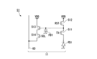
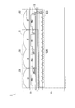
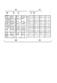
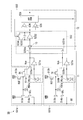
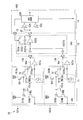
La présente invention comprend : un premier substrat semi-conducteur sur lequel une lumière est incidente ; un second substrat semi-conducteur qui est superposé sur une surface placée du côté opposé d'une surface, côté sur lequel la lumière est incidente sur le premier substrat semi-conducteur ; un nombre n de premiers éléments de conversion photoélectrique qui sont placés sur le premier substrat semi-conducteur à un certain intervalle, et qui génèrent chacun un premier signal de charge obtenu par la conversion photoélectrique de la lumière incidente ; un nombre n de premiers circuits de récupération qui sont placés sur le premier substrat semi-conducteur d'une manière correspondante avec le nombre n respectif de premiers éléments de conversion photoélectrique, qui accumulent chacun le premier signal de charge généré par l'un correspondant des premiers éléments de conversion photoélectrique, et qui émettent, en tant qu'un premier signal de pixel, une tension de signal d'après le premier signal de charge accumulé ; un circuit d'entraînement qui entraîne successivement chacun du nombre n de premiers circuits de récupération et commande à chacun d'entre eux d'émettre le premier signal de pixel ; un nombre m de seconds éléments de conversion photoélectrique qui sont placés sur le second substrat semi-conducteur ou le premier substrat semi-conducteur à un certain intervalle, et qui génèrent chacun un second signal de charge obtenu par la conversion photoélectrique de la lumière incidente ; et un nombre m de seconds circuits de récupération qui émettent chacun successivement un second signal de pixel représentant un changement du, dans le nombre m de seconds éléments de conversion photoélectrique, second signal de charge généré par l'un correspondant des seconds éléments de conversion photoélectrique, chacun du nombre m de seconds circuits de récupération ayant : un circuit de détection qui détecte un changement temporel du second signal de charge généré par l'élément correspondant des seconds éléments de conversion photoélectrique et qui émet, quand un changement dépassant un seuil prédéterminé est détecté, un signal d'événement représentant la direction du changement ; et un circuit de génération de signal de pixel qui est placé sur le second substrat semi-conducteur et qui émet un second signal de pixel obtenu en ajoutant, au signal d'événement, des informations d'adresse représentant la position à laquelle se trouve l'élément correspondant des seconds éléments de conversion photoélectrique, n étant un entier naturel égal ou supérieur à 2, et m étant un entier naturel égal ou supérieur à 2.
Priority Applications (3)
| Application Number | Priority Date | Filing Date | Title |
|---|---|---|---|
| JP2017528048A JP6440844B2 (ja) | 2015-07-14 | 2015-07-14 | 固体撮像装置 |
| PCT/JP2015/070129 WO2017009944A1 (fr) | 2015-07-14 | 2015-07-14 | Dispositif de capture d'image à semi-conducteur |
| US15/865,705 US10218922B2 (en) | 2015-07-14 | 2018-01-09 | Solid-state imaging device |
Applications Claiming Priority (1)
| Application Number | Priority Date | Filing Date | Title |
|---|---|---|---|
| PCT/JP2015/070129 WO2017009944A1 (fr) | 2015-07-14 | 2015-07-14 | Dispositif de capture d'image à semi-conducteur |
Related Child Applications (1)
| Application Number | Title | Priority Date | Filing Date |
|---|---|---|---|
| US15/865,705 Continuation US10218922B2 (en) | 2015-07-14 | 2018-01-09 | Solid-state imaging device |
Publications (1)
| Publication Number | Publication Date |
|---|---|
| WO2017009944A1 true WO2017009944A1 (fr) | 2017-01-19 |
Family
ID=57757114
Family Applications (1)
| Application Number | Title | Priority Date | Filing Date |
|---|---|---|---|
| PCT/JP2015/070129 WO2017009944A1 (fr) | 2015-07-14 | 2015-07-14 | Dispositif de capture d'image à semi-conducteur |
Country Status (3)
| Country | Link |
|---|---|
| US (1) | US10218922B2 (fr) |
| JP (1) | JP6440844B2 (fr) |
| WO (1) | WO2017009944A1 (fr) |
Cited By (12)
| Publication number | Priority date | Publication date | Assignee | Title |
|---|---|---|---|---|
| CN109729292A (zh) * | 2017-10-30 | 2019-05-07 | 索尼半导体解决方案公司 | 固体摄像元件 |
| CN109729291A (zh) * | 2017-10-30 | 2019-05-07 | 索尼半导体解决方案公司 | 固体摄像元件 |
| KR20200012917A (ko) * | 2017-05-26 | 2020-02-05 | 가부시키가이샤 한도오따이 에네루기 켄큐쇼 | 촬상 장치 및 전자 기기 |
| WO2020105301A1 (fr) * | 2018-11-21 | 2020-05-28 | ソニーセミコンダクタソリューションズ株式会社 | Élément d'imagerie à semi-conducteurs et dispositif d'imagerie |
| CN112243536A (zh) * | 2018-03-14 | 2021-01-19 | 索尼高级视觉传感股份公司 | 用3d-ic技术制造的基于事件的视觉传感器 |
| WO2021157386A1 (fr) * | 2020-02-03 | 2021-08-12 | ソニーセミコンダクタソリューションズ株式会社 | Élément d'imagerie à semi-conducteurs et dispositif d'imagerie |
| JP6923240B1 (ja) * | 2021-02-12 | 2021-08-18 | 株式会社SensAI | 固体撮像装置、及び固体撮像装置の駆動方法 |
| WO2021166472A1 (fr) * | 2020-02-17 | 2021-08-26 | ソニーセミコンダクタソリューションズ株式会社 | Dispositif de capteur et procédé de lecture |
| JP2022500974A (ja) * | 2018-09-18 | 2022-01-04 | イニベーション・アー・ゲー | 時間的および空間的コントラストを画像化するための画像センサおよびセンサデバイス |
| JP2022530478A (ja) * | 2019-04-25 | 2022-06-29 | ベイジン・ルイスーヂーシン・テクノロジー・カンパニー・リミテッド | デルタビジョンセンサ |
| JP2023522189A (ja) * | 2020-04-26 | 2023-05-29 | オムニビジョン センサー ソリューション (シャンハイ) カンパニー リミテッド | 画像センサー |
| US11962926B2 (en) | 2020-08-14 | 2024-04-16 | Alpsentek Gmbh | Image sensor with configurable pixel circuit and method |
Families Citing this family (12)
| Publication number | Priority date | Publication date | Assignee | Title |
|---|---|---|---|---|
| US9818777B2 (en) | 2015-11-12 | 2017-11-14 | Stmicroelectronics (Research & Development) Limited | Hybrid analog-digital pixel implemented in a stacked configuration |
| JP7102159B2 (ja) * | 2018-02-09 | 2022-07-19 | キヤノン株式会社 | 光電変換装置、撮像システム、および、移動体 |
| US10535695B2 (en) * | 2018-03-13 | 2020-01-14 | Stmicroelectronics (Research & Development) Limited | Stacked wafer arrangement for global shutter pixels utilizing capacitive deep trench isolations |
| JP7175730B2 (ja) | 2018-12-05 | 2022-11-21 | 株式会社ソニー・インタラクティブエンタテインメント | 信号処理装置、電子機器、センサ装置、信号処理方法およびプログラム |
| JP2020096225A (ja) * | 2018-12-10 | 2020-06-18 | ソニーセミコンダクタソリューションズ株式会社 | 撮像装置及び電子機器 |
| US11483506B2 (en) | 2019-05-29 | 2022-10-25 | Raytheon Company | Continuously integrating digital pixel imager |
| WO2021021453A1 (fr) * | 2019-07-26 | 2021-02-04 | Ocelot Laboratories Llc | Circuit de lecture de pixel capable de détecter une intensité lumineuse et un changement de contraste et comportant un photodétecteur partagé |
| US11062679B2 (en) | 2019-09-06 | 2021-07-13 | Sony Semiconductor Solutions Corporations | Imaging devices and imaging apparatuses, and methods for the same |
| US20230059890A1 (en) * | 2020-02-13 | 2023-02-23 | Sony Semiconductor Solutions Corporation | Solid-state imaging device and imaging device |
| JP2021164017A (ja) * | 2020-03-31 | 2021-10-11 | 株式会社村田製作所 | 高周波モジュール及び通信装置 |
| CN115668972A (zh) * | 2020-06-19 | 2023-01-31 | 索尼半导体解决方案公司 | 摄像装置 |
| JP2022003672A (ja) * | 2020-06-23 | 2022-01-11 | キヤノン株式会社 | 光電変換装置、光電変換システム、および移動体 |
Citations (3)
| Publication number | Priority date | Publication date | Assignee | Title |
|---|---|---|---|---|
| WO2006022077A1 (fr) * | 2004-08-23 | 2006-03-02 | Sony Corporation | Dispositif de sélection d’image, procédé de traitement du résultat de la sélection d’image et circuit intégré |
| JP2010510732A (ja) * | 2006-11-23 | 2010-04-02 | エーアイティー オーストリアン インスティテュート オブ テクノロジー ゲゼルシャフト ミット ベシュレンクテル ハフツング | 電子形式の画像を生成する方法、画像生成用画像センサのための画像素子ならびに画像センサ |
| JP2015128284A (ja) * | 2013-11-29 | 2015-07-09 | キヤノン株式会社 | 撮像装置及び携帯電話機 |
Family Cites Families (5)
| Publication number | Priority date | Publication date | Assignee | Title |
|---|---|---|---|---|
| US7088860B2 (en) * | 2001-03-28 | 2006-08-08 | Canon Kabushiki Kaisha | Dynamically reconfigurable signal processing circuit, pattern recognition apparatus, and image processing apparatus |
| US8526500B2 (en) * | 2009-08-11 | 2013-09-03 | Seiko Epson Corporation | System and method for global inter-frame motion detection in video sequences |
| KR20140056986A (ko) * | 2012-11-02 | 2014-05-12 | 삼성전자주식회사 | 모션 센서 어레이 장치, 상기 모선 센서 어레이를 이용한 거리 센싱 시스템, 및 거리 센싱 방법 |
| WO2016003451A1 (fr) * | 2014-07-02 | 2016-01-07 | The Johns Hopkins University | Circuit de photodétection et procédé de fonctionnement associé |
| CN108574793B (zh) * | 2017-03-08 | 2022-05-10 | 三星电子株式会社 | 被配置为重新生成时间戳的图像处理设备及包括其在内的电子设备 |
-
2015
- 2015-07-14 WO PCT/JP2015/070129 patent/WO2017009944A1/fr active Application Filing
- 2015-07-14 JP JP2017528048A patent/JP6440844B2/ja active Active
-
2018
- 2018-01-09 US US15/865,705 patent/US10218922B2/en active Active
Patent Citations (3)
| Publication number | Priority date | Publication date | Assignee | Title |
|---|---|---|---|---|
| WO2006022077A1 (fr) * | 2004-08-23 | 2006-03-02 | Sony Corporation | Dispositif de sélection d’image, procédé de traitement du résultat de la sélection d’image et circuit intégré |
| JP2010510732A (ja) * | 2006-11-23 | 2010-04-02 | エーアイティー オーストリアン インスティテュート オブ テクノロジー ゲゼルシャフト ミット ベシュレンクテル ハフツング | 電子形式の画像を生成する方法、画像生成用画像センサのための画像素子ならびに画像センサ |
| JP2015128284A (ja) * | 2013-11-29 | 2015-07-09 | キヤノン株式会社 | 撮像装置及び携帯電話機 |
Cited By (39)
| Publication number | Priority date | Publication date | Assignee | Title |
|---|---|---|---|---|
| KR20200012917A (ko) * | 2017-05-26 | 2020-02-05 | 가부시키가이샤 한도오따이 에네루기 켄큐쇼 | 촬상 장치 및 전자 기기 |
| US11728355B2 (en) | 2017-05-26 | 2023-08-15 | Semiconductor Energy Laboratory Co., Ltd. | Imaging device and electronic device |
| KR102554664B1 (ko) * | 2017-05-26 | 2023-07-11 | 가부시키가이샤 한도오따이 에네루기 켄큐쇼 | 촬상 장치 및 전자 기기 |
| US11546542B2 (en) | 2017-10-30 | 2023-01-03 | Sony Semiconductor Solutions Corporation | Solid-state imaging device |
| KR20200073170A (ko) * | 2017-10-30 | 2020-06-23 | 소니 세미컨덕터 솔루션즈 가부시키가이샤 | 고체 촬상 소자 |
| US11245861B2 (en) | 2017-10-30 | 2022-02-08 | Sony Semiconductor Solutions Corporation | Solid-state imaging element |
| CN114339098A (zh) * | 2017-10-30 | 2022-04-12 | 索尼半导体解决方案公司 | 固体摄像元件 |
| KR20200123865A (ko) * | 2017-10-30 | 2020-10-30 | 소니 세미컨덕터 솔루션즈 가부시키가이샤 | 고체 촬상 소자 |
| US11895422B2 (en) | 2017-10-30 | 2024-02-06 | Sony Semiconductor Solutions Corporation | Solid-state imaging device |
| JP2021044847A (ja) * | 2017-10-30 | 2021-03-18 | ソニーセミコンダクタソリューションズ株式会社 | 固体撮像素子 |
| CN112601036A (zh) * | 2017-10-30 | 2021-04-02 | 索尼半导体解决方案公司 | 事件检测传感器 |
| EP3813356A1 (fr) * | 2017-10-30 | 2021-04-28 | Sony Semiconductor Solutions Corporation | Dispositif d'imagerie à semi-conducteurs |
| US11082656B2 (en) | 2017-10-30 | 2021-08-03 | Sony Semiconductor Solutions Corporation | Solid-state imaging device |
| CN109729291A (zh) * | 2017-10-30 | 2019-05-07 | 索尼半导体解决方案公司 | 固体摄像元件 |
| KR102561079B1 (ko) * | 2017-10-30 | 2023-07-27 | 소니 세미컨덕터 솔루션즈 가부시키가이샤 | 고체 촬상 소자 |
| EP3576404A4 (fr) * | 2017-10-30 | 2020-01-15 | Sony Semiconductor Solutions Corporation | Élément de capture d'image à semi-conducteurs |
| CN109729291B (zh) * | 2017-10-30 | 2021-10-22 | 索尼半导体解决方案公司 | 固体摄像元件 |
| CN109729292B (zh) * | 2017-10-30 | 2021-11-16 | 索尼半导体解决方案公司 | 固体摄像元件 |
| US11659291B2 (en) | 2017-10-30 | 2023-05-23 | Sony Semiconductor Solutions Corporation | Solid-state imaging element |
| CN109729292A (zh) * | 2017-10-30 | 2019-05-07 | 索尼半导体解决方案公司 | 固体摄像元件 |
| US11490045B2 (en) | 2017-10-30 | 2022-11-01 | Sony Semiconductor Solutions Corporation | Solid-state imaging device |
| EP3582491A4 (fr) * | 2017-10-30 | 2020-03-25 | Sony Semiconductor Solutions Corporation | Élément de capture d'image à semi-conducteurs |
| KR102453118B1 (ko) * | 2017-10-30 | 2022-10-07 | 소니 세미컨덕터 솔루션즈 가부시키가이샤 | 고체 촬상 소자 |
| JP7141440B2 (ja) | 2017-10-30 | 2022-09-22 | ソニーセミコンダクタソリューションズ株式会社 | 固体撮像素子 |
| CN112243536A (zh) * | 2018-03-14 | 2021-01-19 | 索尼高级视觉传感股份公司 | 用3d-ic技术制造的基于事件的视觉传感器 |
| US11652126B2 (en) | 2018-03-14 | 2023-05-16 | Sony Advanced Visual Sensing Ag | Event-based vision sensor manufactured with 3D-IC technology |
| JP7175051B2 (ja) | 2018-09-18 | 2022-11-18 | イニベーション・アー・ゲー | 時間的および空間的コントラストを画像化するための画像センサおよびセンサデバイス |
| JP2022500974A (ja) * | 2018-09-18 | 2022-01-04 | イニベーション・アー・ゲー | 時間的および空間的コントラストを画像化するための画像センサおよびセンサデバイス |
| US11917317B2 (en) | 2018-11-21 | 2024-02-27 | Sony Semiconductor Solutions Corporation | Solid-state imaging element and imaging device that detects address event |
| WO2020105301A1 (fr) * | 2018-11-21 | 2020-05-28 | ソニーセミコンダクタソリューションズ株式会社 | Élément d'imagerie à semi-conducteurs et dispositif d'imagerie |
| JP2022530478A (ja) * | 2019-04-25 | 2022-06-29 | ベイジン・ルイスーヂーシン・テクノロジー・カンパニー・リミテッド | デルタビジョンセンサ |
| JP7453641B2 (ja) | 2019-04-25 | 2024-03-21 | ベイジン・ルイスーヂーシン・テクノロジー・カンパニー・リミテッド | デルタビジョンセンサ |
| WO2021157386A1 (fr) * | 2020-02-03 | 2021-08-12 | ソニーセミコンダクタソリューションズ株式会社 | Élément d'imagerie à semi-conducteurs et dispositif d'imagerie |
| WO2021166472A1 (fr) * | 2020-02-17 | 2021-08-26 | ソニーセミコンダクタソリューションズ株式会社 | Dispositif de capteur et procédé de lecture |
| JP2023522189A (ja) * | 2020-04-26 | 2023-05-29 | オムニビジョン センサー ソリューション (シャンハイ) カンパニー リミテッド | 画像センサー |
| JP7405328B2 (ja) | 2020-04-26 | 2023-12-26 | オムニビジョン センサー ソリューション (シャンハイ) カンパニー リミテッド | 画像センサー |
| US11962926B2 (en) | 2020-08-14 | 2024-04-16 | Alpsentek Gmbh | Image sensor with configurable pixel circuit and method |
| JP6923240B1 (ja) * | 2021-02-12 | 2021-08-18 | 株式会社SensAI | 固体撮像装置、及び固体撮像装置の駆動方法 |
| JP2022123740A (ja) * | 2021-02-12 | 2022-08-24 | 株式会社SensAI | 固体撮像装置、及び固体撮像装置の駆動方法 |
Also Published As
| Publication number | Publication date |
|---|---|
| US20180152644A1 (en) | 2018-05-31 |
| JP6440844B2 (ja) | 2018-12-19 |
| JPWO2017009944A1 (ja) | 2017-12-14 |
| US10218922B2 (en) | 2019-02-26 |
Similar Documents
| Publication | Publication Date | Title |
|---|---|---|
| JP6440844B2 (ja) | 固体撮像装置 | |
| US11588991B2 (en) | Solid-state imaging device and electronic camera | |
| US10321081B2 (en) | Solid-state imaging device | |
| JP2021121123A (ja) | 固体撮像装置およびその駆動方法、並びに電子機器 | |
| JP5026951B2 (ja) | 撮像素子の駆動装置、撮像素子の駆動方法、撮像装置、及び撮像素子 | |
| WO2015151790A1 (fr) | Élément d'imagerie à semi-conducteur, dispositif électronique et procédé d'imagerie | |
| JP6026102B2 (ja) | 固体撮像素子および電子機器 | |
| WO2013172205A1 (fr) | Dispositif d'imagerie et procédé d'imagerie, appareil électronique ainsi que programme | |
| JP6457738B2 (ja) | 固体撮像装置および撮像装置 | |
| JP2010245951A (ja) | 撮像素子及び撮像装置 | |
| US20240089629A1 (en) | Image sensor and imaging device | |
| JP2014175992A (ja) | 固体撮像素子及びこれを用いた撮像装置 | |
| JP6733159B2 (ja) | 撮像素子、及び撮像装置 | |
| JP2016103513A (ja) | 撮像素子および撮像装置 | |
| JP6217338B2 (ja) | 固体撮像素子及び撮像装置 | |
| JP2020014255A (ja) | 撮像素子及び撮像装置 | |
| JP2016019232A (ja) | 撮像素子及び撮像装置 | |
| JP7294406B2 (ja) | 撮像素子、及び、撮像装置 | |
| JP2019097058A (ja) | 固体撮像装置、固体撮像装置の製造方法、および電子機器 | |
| JP7247975B2 (ja) | 撮像素子及び撮像装置 | |
| JP4848349B2 (ja) | 撮像装置及び固体撮像素子の駆動方法 | |
| JP5958497B2 (ja) | 固体撮像装置および電子カメラ | |
| JP5256084B2 (ja) | 撮像装置及び撮像装置の駆動方法 | |
| JP2016076886A (ja) | 撮像装置及びその形成方法 |
Legal Events
| Date | Code | Title | Description |
|---|---|---|---|
| 121 | Ep: the epo has been informed by wipo that ep was designated in this application |
Ref document number: 15898257 Country of ref document: EP Kind code of ref document: A1 |
|
| ENP | Entry into the national phase |
Ref document number: 2017528048 Country of ref document: JP Kind code of ref document: A |
|
| NENP | Non-entry into the national phase |
Ref country code: DE |
|
| 122 | Ep: pct application non-entry in european phase |
Ref document number: 15898257 Country of ref document: EP Kind code of ref document: A1 |