WO2017009944A1 - Solid-state image pickup device - Google Patents
Solid-state image pickup device Download PDFInfo
- Publication number
- WO2017009944A1 WO2017009944A1 PCT/JP2015/070129 JP2015070129W WO2017009944A1 WO 2017009944 A1 WO2017009944 A1 WO 2017009944A1 JP 2015070129 W JP2015070129 W JP 2015070129W WO 2017009944 A1 WO2017009944 A1 WO 2017009944A1
- Authority
- WO
- WIPO (PCT)
- Prior art keywords
- pixel
- photoelectric conversion
- semiconductor substrate
- solid
- imaging device
- Prior art date
Links
- 238000001514 detection method Methods 0.000 claims abstract description 417
- 239000000758 substrate Substances 0.000 claims abstract description 298
- 239000004065 semiconductor Substances 0.000 claims abstract description 296
- 238000006243 chemical reaction Methods 0.000 claims abstract description 265
- 230000008859 change Effects 0.000 claims abstract description 49
- 230000002123 temporal effect Effects 0.000 claims abstract description 14
- 238000003384 imaging method Methods 0.000 claims description 359
- 230000007274 generation of a signal involved in cell-cell signaling Effects 0.000 abstract description 2
- 239000003990 capacitor Substances 0.000 description 117
- 230000007423 decrease Effects 0.000 description 31
- 238000010586 diagram Methods 0.000 description 22
- 230000003321 amplification Effects 0.000 description 21
- 238000003199 nucleic acid amplification method Methods 0.000 description 21
- 238000000034 method Methods 0.000 description 14
- 239000000470 constituent Substances 0.000 description 8
- 238000007792 addition Methods 0.000 description 7
- 230000009977 dual effect Effects 0.000 description 4
- 230000004048 modification Effects 0.000 description 2
- 238000012986 modification Methods 0.000 description 2
- XUIMIQQOPSSXEZ-UHFFFAOYSA-N Silicon Chemical compound [Si] XUIMIQQOPSSXEZ-UHFFFAOYSA-N 0.000 description 1
- 238000004364 calculation method Methods 0.000 description 1
- 239000003086 colorant Substances 0.000 description 1
- 230000003247 decreasing effect Effects 0.000 description 1
- 230000006866 deterioration Effects 0.000 description 1
- 230000000694 effects Effects 0.000 description 1
- 230000006872 improvement Effects 0.000 description 1
- 238000005304 joining Methods 0.000 description 1
- 238000004519 manufacturing process Methods 0.000 description 1
- 239000011159 matrix material Substances 0.000 description 1
- 230000035515 penetration Effects 0.000 description 1
- 230000002093 peripheral effect Effects 0.000 description 1
- 238000007747 plating Methods 0.000 description 1
- 230000004044 response Effects 0.000 description 1
- 229910052710 silicon Inorganic materials 0.000 description 1
- 239000010703 silicon Substances 0.000 description 1
- 238000006467 substitution reaction Methods 0.000 description 1
- 230000001360 synchronised effect Effects 0.000 description 1
- 238000007740 vapor deposition Methods 0.000 description 1
Images


Classifications
-
- H—ELECTRICITY
- H01—ELECTRIC ELEMENTS
- H01L—SEMICONDUCTOR DEVICES NOT COVERED BY CLASS H10
- H01L27/00—Devices consisting of a plurality of semiconductor or other solid-state components formed in or on a common substrate
- H01L27/14—Devices consisting of a plurality of semiconductor or other solid-state components formed in or on a common substrate including semiconductor components sensitive to infrared radiation, light, electromagnetic radiation of shorter wavelength or corpuscular radiation and specially adapted either for the conversion of the energy of such radiation into electrical energy or for the control of electrical energy by such radiation
- H01L27/144—Devices controlled by radiation
- H01L27/146—Imager structures
- H01L27/14601—Structural or functional details thereof
- H01L27/14603—Special geometry or disposition of pixel-elements, address-lines or gate-electrodes
- H01L27/14605—Structural or functional details relating to the position of the pixel elements, e.g. smaller pixel elements in the center of the imager compared to pixel elements at the periphery
-
- H—ELECTRICITY
- H01—ELECTRIC ELEMENTS
- H01L—SEMICONDUCTOR DEVICES NOT COVERED BY CLASS H10
- H01L27/00—Devices consisting of a plurality of semiconductor or other solid-state components formed in or on a common substrate
- H01L27/14—Devices consisting of a plurality of semiconductor or other solid-state components formed in or on a common substrate including semiconductor components sensitive to infrared radiation, light, electromagnetic radiation of shorter wavelength or corpuscular radiation and specially adapted either for the conversion of the energy of such radiation into electrical energy or for the control of electrical energy by such radiation
- H01L27/144—Devices controlled by radiation
- H01L27/146—Imager structures
- H01L27/14601—Structural or functional details thereof
- H01L27/14603—Special geometry or disposition of pixel-elements, address-lines or gate-electrodes
- H01L27/14607—Geometry of the photosensitive area
-
- H—ELECTRICITY
- H01—ELECTRIC ELEMENTS
- H01L—SEMICONDUCTOR DEVICES NOT COVERED BY CLASS H10
- H01L27/00—Devices consisting of a plurality of semiconductor or other solid-state components formed in or on a common substrate
- H01L27/14—Devices consisting of a plurality of semiconductor or other solid-state components formed in or on a common substrate including semiconductor components sensitive to infrared radiation, light, electromagnetic radiation of shorter wavelength or corpuscular radiation and specially adapted either for the conversion of the energy of such radiation into electrical energy or for the control of electrical energy by such radiation
- H01L27/144—Devices controlled by radiation
- H01L27/146—Imager structures
- H01L27/14601—Structural or functional details thereof
- H01L27/14609—Pixel-elements with integrated switching, control, storage or amplification elements
- H01L27/1461—Pixel-elements with integrated switching, control, storage or amplification elements characterised by the photosensitive area
-
- H—ELECTRICITY
- H01—ELECTRIC ELEMENTS
- H01L—SEMICONDUCTOR DEVICES NOT COVERED BY CLASS H10
- H01L27/00—Devices consisting of a plurality of semiconductor or other solid-state components formed in or on a common substrate
- H01L27/14—Devices consisting of a plurality of semiconductor or other solid-state components formed in or on a common substrate including semiconductor components sensitive to infrared radiation, light, electromagnetic radiation of shorter wavelength or corpuscular radiation and specially adapted either for the conversion of the energy of such radiation into electrical energy or for the control of electrical energy by such radiation
- H01L27/144—Devices controlled by radiation
- H01L27/146—Imager structures
- H01L27/14601—Structural or functional details thereof
- H01L27/14634—Assemblies, i.e. Hybrid structures
-
- H—ELECTRICITY
- H01—ELECTRIC ELEMENTS
- H01L—SEMICONDUCTOR DEVICES NOT COVERED BY CLASS H10
- H01L27/00—Devices consisting of a plurality of semiconductor or other solid-state components formed in or on a common substrate
- H01L27/14—Devices consisting of a plurality of semiconductor or other solid-state components formed in or on a common substrate including semiconductor components sensitive to infrared radiation, light, electromagnetic radiation of shorter wavelength or corpuscular radiation and specially adapted either for the conversion of the energy of such radiation into electrical energy or for the control of electrical energy by such radiation
- H01L27/144—Devices controlled by radiation
- H01L27/146—Imager structures
- H01L27/14643—Photodiode arrays; MOS imagers
-
- H—ELECTRICITY
- H04—ELECTRIC COMMUNICATION TECHNIQUE
- H04N—PICTORIAL COMMUNICATION, e.g. TELEVISION
- H04N25/00—Circuitry of solid-state image sensors [SSIS]; Control thereof
- H04N25/40—Extracting pixel data from image sensors by controlling scanning circuits, e.g. by modifying the number of pixels sampled or to be sampled
- H04N25/44—Extracting pixel data from image sensors by controlling scanning circuits, e.g. by modifying the number of pixels sampled or to be sampled by partially reading an SSIS array
-
- H—ELECTRICITY
- H04—ELECTRIC COMMUNICATION TECHNIQUE
- H04N—PICTORIAL COMMUNICATION, e.g. TELEVISION
- H04N25/00—Circuitry of solid-state image sensors [SSIS]; Control thereof
- H04N25/70—SSIS architectures; Circuits associated therewith
- H04N25/76—Addressed sensors, e.g. MOS or CMOS sensors
- H04N25/77—Pixel circuitry, e.g. memories, A/D converters, pixel amplifiers, shared circuits or shared components
-
- H—ELECTRICITY
- H04—ELECTRIC COMMUNICATION TECHNIQUE
- H04N—PICTORIAL COMMUNICATION, e.g. TELEVISION
- H04N25/00—Circuitry of solid-state image sensors [SSIS]; Control thereof
- H04N25/70—SSIS architectures; Circuits associated therewith
- H04N25/79—Arrangements of circuitry being divided between different or multiple substrates, chips or circuit boards, e.g. stacked image sensors
-
- H—ELECTRICITY
- H01—ELECTRIC ELEMENTS
- H01L—SEMICONDUCTOR DEVICES NOT COVERED BY CLASS H10
- H01L27/00—Devices consisting of a plurality of semiconductor or other solid-state components formed in or on a common substrate
- H01L27/14—Devices consisting of a plurality of semiconductor or other solid-state components formed in or on a common substrate including semiconductor components sensitive to infrared radiation, light, electromagnetic radiation of shorter wavelength or corpuscular radiation and specially adapted either for the conversion of the energy of such radiation into electrical energy or for the control of electrical energy by such radiation
- H01L27/144—Devices controlled by radiation
- H01L27/146—Imager structures
- H01L27/14601—Structural or functional details thereof
- H01L27/1462—Coatings
- H01L27/14621—Colour filter arrangements
-
- H—ELECTRICITY
- H01—ELECTRIC ELEMENTS
- H01L—SEMICONDUCTOR DEVICES NOT COVERED BY CLASS H10
- H01L27/00—Devices consisting of a plurality of semiconductor or other solid-state components formed in or on a common substrate
- H01L27/14—Devices consisting of a plurality of semiconductor or other solid-state components formed in or on a common substrate including semiconductor components sensitive to infrared radiation, light, electromagnetic radiation of shorter wavelength or corpuscular radiation and specially adapted either for the conversion of the energy of such radiation into electrical energy or for the control of electrical energy by such radiation
- H01L27/144—Devices controlled by radiation
- H01L27/146—Imager structures
- H01L27/14601—Structural or functional details thereof
- H01L27/14625—Optical elements or arrangements associated with the device
- H01L27/14627—Microlenses
-
- H—ELECTRICITY
- H01—ELECTRIC ELEMENTS
- H01L—SEMICONDUCTOR DEVICES NOT COVERED BY CLASS H10
- H01L27/00—Devices consisting of a plurality of semiconductor or other solid-state components formed in or on a common substrate
- H01L27/14—Devices consisting of a plurality of semiconductor or other solid-state components formed in or on a common substrate including semiconductor components sensitive to infrared radiation, light, electromagnetic radiation of shorter wavelength or corpuscular radiation and specially adapted either for the conversion of the energy of such radiation into electrical energy or for the control of electrical energy by such radiation
- H01L27/144—Devices controlled by radiation
- H01L27/146—Imager structures
- H01L27/14601—Structural or functional details thereof
- H01L27/14636—Interconnect structures
-
- H—ELECTRICITY
- H04—ELECTRIC COMMUNICATION TECHNIQUE
- H04N—PICTORIAL COMMUNICATION, e.g. TELEVISION
- H04N5/00—Details of television systems
- H04N5/14—Picture signal circuitry for video frequency region
- H04N5/144—Movement detection
Landscapes
- Engineering & Computer Science (AREA)
- Physics & Mathematics (AREA)
- Power Engineering (AREA)
- Electromagnetism (AREA)
- Condensed Matter Physics & Semiconductors (AREA)
- General Physics & Mathematics (AREA)
- Computer Hardware Design (AREA)
- Microelectronics & Electronic Packaging (AREA)
- Multimedia (AREA)
- Signal Processing (AREA)
- Solid State Image Pick-Up Elements (AREA)
- Transforming Light Signals Into Electric Signals (AREA)
Abstract
The present invention has: a first semiconductor substrate on which light is incident; a second semiconductor substrate that is layered on a surface located on the opposite side of a surface on which side the light is incident on the first semiconductor substrate; n-number of first photoelectric conversion elements that are disposed on the first semiconductor substrate at a certain interval, and that each generate a first charge signal obtained through photoelectric conversion of the incident light; n-number of first retrieval circuits that are disposed on the first semiconductor substrate in a corresponding manner with the respective n-number of first photoelectric conversion elements, that each accumulate the first charge signal generated by a corresponding one of the first photoelectric conversion elements, and that each output, as a first pixel signal, a signal voltage in accordance with the accumulated first charge signal; a drive circuit that successively drives each of the n-number of first retrieval circuits and causes each thereof to output the first pixel signal; m-number of second photoelectric conversion elements that are disposed on the second semiconductor substrate or the first semiconductor substrate at a certain interval, and that each generate a second charge signal obtained through photoelectric conversion of the incident light; and m-number of second retrieval circuits that each successively output a second pixel signal representing a change in, among the m-number of second photoelectric conversion elements, the second charge signal generated by a corresponding one of the second photoelectric conversion elements, wherein each of the m-number of second retrieval circuits has: a detection circuit that detects a temporal change in the second charge signal generated by the corresponding one of the second photoelectric conversion elements and that outputs, when a change exceeding a predetermined threshold is detected, an event signal representing the direction of the change; and a pixel signal generation circuit that is disposed on the second semiconductor substrate and that outputs a second pixel signal obtained by adding, to the event signal, address information representing the position where the corresponding one of the second photoelectric conversion elements is disposed, wherein n is a natural number equal to or larger than 2 and m is a natural number equal to or larger than 2.
Description
本発明は、固体撮像装置に関する。
The present invention relates to a solid-state imaging device.
従来から、被写体の動きを検出する動き検出の技術がある。従来の動き検出では、予め定めたフレームの間隔で撮影したそれぞれの画像の差分をとることによって、動いている被写体を捕らえている。このため、従来の動き検出では、被写体の動きをフレームの間隔でしか検出することができない。つまり、被写体の動きを逐次検出することができない。
Conventionally, there is a motion detection technique for detecting the motion of a subject. In the conventional motion detection, a moving subject is captured by taking a difference between respective images taken at predetermined frame intervals. For this reason, in the conventional motion detection, the motion of the subject can be detected only at the frame interval. That is, the movement of the subject cannot be detected sequentially.
そこで、近年では、例えば、非特許文献1に開示されたように、被写体の動きに応じた信号の変化を検出することによって、被写体の動きを逐次検出する動き検出と、通常の撮影とを両立する固体撮像装置の技術が提案されている。非特許文献1に提案された固体撮像装置では、それぞれの画素に、入射した光を光電変換する1個の光電変換素子(フォトダイオード)を備え、通常の撮影による電荷信号を読み出すAPS(Active Pixel Sensor)読み出しと、動き検出のための電荷信号を読み出すAER(Address Event Representation)読み出しとを非同期に行うことができる。
Therefore, in recent years, for example, as disclosed in Non-Patent Document 1, by detecting a change in a signal in accordance with the movement of the subject, both motion detection for sequentially detecting the motion of the subject and normal shooting are compatible. A technique for a solid-state imaging device has been proposed. In the solid-state imaging device proposed in Non-Patent Document 1, each pixel is provided with one photoelectric conversion element (photodiode) that photoelectrically converts incident light, and an APS (Active Pixel) that reads out a charge signal from normal imaging. Sensor (Sensor) readout and AER (Address Event Representation) readout for reading out a charge signal for motion detection can be performed asynchronously.
非特許文献1に提案された固体撮像装置では、動き検出の際に、フォトダイオードが光電変換している電荷信号の時間的な変化を検出し、電荷信号の大きさが予め定めた閾値を超えた画素からのみ、電荷信号が変化した方向、つまり、電荷信号の大きさの増減を表すパルス信号をAER読み出しで出力している。このとき、AER読み出しによって出力されるパルス信号には、パルス信号を出力する画素、つまり、被写体の動きを検出した画素の位置を表すアドレス情報も付加されている。
In the solid-state imaging device proposed in Non-Patent Document 1, when motion is detected, a temporal change in the charge signal photoelectrically converted by the photodiode is detected, and the magnitude of the charge signal exceeds a predetermined threshold value. A pulse signal indicating the direction in which the charge signal has changed, that is, an increase / decrease in the magnitude of the charge signal, is output by AER readout only from the pixels. At this time, address information indicating the position of the pixel that outputs the pulse signal, that is, the pixel that detected the movement of the subject is also added to the pulse signal output by the AER readout.
これにより、非特許文献1に提案された固体撮像装置では、被写体の動きを検出した画素の位置を、通常の撮影において電荷信号を読み出すフレームのタイミングとは関係しない非同期のタイミングで抽出することができる。このことにより、非特許文献1に提案された固体撮像装置では、通常の撮影におけるフレームレートよりも高速に、動いている被写体を捕らえることができる。
Thereby, in the solid-state imaging device proposed in Non-Patent Document 1, the position of the pixel where the movement of the subject is detected can be extracted at an asynchronous timing that is not related to the timing of the frame from which the charge signal is read in normal imaging. it can. As a result, the solid-state imaging device proposed in Non-Patent Document 1 can capture a moving subject at a higher speed than the frame rate in normal shooting.
しかしながら、非特許文献1に提案された固体撮像装置では、電荷信号が変化した方向を検出する論理回路や、パルス信号にアドレス情報を付加するための論理回路を、それぞれの画素に備える必要がある。このため、非特許文献1に提案された固体撮像装置では、画素への論理回路の追加に伴って、フォトダイオードの面積を小さくすることが必要になってしまう。これにより、非特許文献1に提案された固体撮像装置では、フォトダイオードが入射した光を光電変換する電荷信号のレベルが低下してしまう。このため、非特許文献1に提案された固体撮像装置では、APS読み出しによって読み出す通常の撮影で得る電荷信号のレベルの低下によって、撮影した通常の画像の画質が低下してしまう。
However, in the solid-state imaging device proposed in Non-Patent Document 1, it is necessary to provide each pixel with a logic circuit that detects the direction in which the charge signal has changed and a logic circuit that adds address information to the pulse signal. . For this reason, in the solid-state imaging device proposed in Non-Patent Document 1, it is necessary to reduce the area of the photodiode as the logic circuit is added to the pixel. As a result, in the solid-state imaging device proposed in Non-Patent Document 1, the level of the charge signal that photoelectrically converts light incident on the photodiode is lowered. For this reason, in the solid-state imaging device proposed in Non-Patent Document 1, the image quality of a captured normal image is deteriorated due to a decrease in the level of a charge signal obtained by normal imaging read by APS readout.
また、電荷信号が変化した方向を検出する論理回路や、パルス信号にアドレス情報を付加するための論理回路をそれぞれの画素に備えるということは、フォトダイオードの面積を小さくして画素数を増加することも困難になるため、固体撮像装置の高画素化を阻害する要因にもなる。
Further, providing each pixel with a logic circuit that detects the direction in which the charge signal has changed and a logic circuit for adding address information to the pulse signal increase the number of pixels by reducing the area of the photodiode. This also makes it difficult to increase the number of pixels of the solid-state imaging device.
また、フォトダイオードが光電変換する電荷信号のレベルが低下するということは、動き検出において時間的な変化を検出するための電荷信号のレベルも低下するということであり、動き検出の精度が低下してしまうことにもつながる。そこで、動き検出の精度の低下を抑えるために、パルス信号を増幅して出力する増幅回路(アンプ)をさらに設けることも考えられるが、この場合、さらに設けたアンプも論理回路に含まれるため、フォトダイオードの面積をさらに小さくすることが必要となり、上述したような、通常の撮影おける画質の低下や、固体撮像装置の高画素化の問題がより顕著になってしまう。
In addition, a decrease in the level of the charge signal photoelectrically converted by the photodiode means that the level of the charge signal for detecting a temporal change in motion detection also decreases, and the accuracy of motion detection decreases. It also leads to that. Therefore, in order to suppress a decrease in the accuracy of motion detection, it is conceivable to further provide an amplifier circuit (amplifier) that amplifies and outputs the pulse signal, but in this case, the further provided amplifier is also included in the logic circuit. It is necessary to further reduce the area of the photodiode, and the above-described problems of deterioration in image quality in normal photographing and increase in the number of pixels of the solid-state imaging device become more remarkable.
本発明は、上記の課題に基づいてなされたものであり、被写体の動きを逐次検出する動き検出と通常の撮影とを両立する固体撮像装置において、動き検出の精度を低下させることなく、通常の撮影おける画質を向上させることができる固体撮像装置を提供することを目的としている。
The present invention has been made based on the above-described problem, and in a solid-state imaging device that achieves both motion detection for sequentially detecting the motion of a subject and normal shooting, the normal detection is performed without reducing the accuracy of motion detection. An object of the present invention is to provide a solid-state imaging device capable of improving image quality in photographing.
本発明の第1の態様によれば、固体撮像装置は、光が入射する第1の半導体基板と、前記第1の半導体基板に光が入射する側の面と反対側の面に積層される第2の半導体基板と、前記第1の半導体基板に周期的に配置され、入射した光を光電変換した第1の電荷信号を発生するn個の第1の光電変換素子と、前記第1の半導体基板に、前記n個の第1の光電変換素子のそれぞれに対応して配置され、対応する1個の前記第1の光電変換素子が発生した前記第1の電荷信号を蓄積し、蓄積した前記第1の電荷信号に応じた信号電圧を第1の画素信号として出力するn個の第1の読み出し回路と、前記n個の第1の読み出し回路のそれぞれを順次駆動して前記第1の画素信号のそれぞれを出力させる駆動回路と、前記第1の半導体基板および前記第2の半導体基板のいずれか一方に周期的に配置され、入射した光を光電変換した第2の電荷信号を発生するm個の第2の光電変換素子と、前記m個の第2の光電変換素子の内、対応する1個の前記第2の光電変換素子が発生した前記第2の電荷信号の変化を表す第2の画素信号を逐次出力するm個の第2の読み出し回路と、を有し、前記m個の第2の読み出し回路のそれぞれは、対応する1個の前記第2の光電変換素子が発生した前記第2の電荷信号の時間的な変化を検出し、予め定めた閾値を超える変化を検出したときに、変化した方向を表すイベント信号を出力する検出回路と、前記第2の半導体基板に配置され、前記イベント信号に、対応する1個の前記第2の光電変換素子が配置された位置を表すアドレス情報を付加した前記第2の画素信号を出力する画素信号生成回路と、を有し、前記nは2以上の自然数であり、前記mは2以上の自然数である。
According to the first aspect of the present invention, the solid-state imaging device is stacked on a first semiconductor substrate on which light is incident and a surface opposite to the surface on which light is incident on the first semiconductor substrate. A second semiconductor substrate, n first photoelectric conversion elements that are periodically disposed on the first semiconductor substrate and generate a first charge signal obtained by photoelectrically converting incident light, and the first semiconductor substrate The first charge signal generated by the corresponding one of the first photoelectric conversion elements is stored and stored on the semiconductor substrate in correspondence with each of the n first photoelectric conversion elements. Each of the n first readout circuits that output a signal voltage corresponding to the first charge signal as a first pixel signal and the n first readout circuits are sequentially driven to perform the first A driving circuit for outputting each of the pixel signals, the first semiconductor substrate and the front circuit; The m second photoelectric conversion elements that are periodically arranged on any one of the second semiconductor substrates and generate a second charge signal obtained by photoelectrically converting incident light, and the m second photoelectric conversion elements. M second readout circuits that sequentially output a second pixel signal representing a change in the second charge signal generated by the corresponding one of the second photoelectric conversion elements among the conversion elements; Each of the m second readout circuits detects a temporal change in the second charge signal generated by the corresponding one of the second photoelectric conversion elements, and determines a predetermined threshold value. A detection circuit that outputs an event signal indicating the changed direction when a change exceeding 1 is detected, and one second photoelectric conversion element that is disposed on the second semiconductor substrate and corresponds to the event signal The address information indicating the position where the A pixel signal generating circuit for outputting a pixel signal of the said n is a natural number of 2 or more, the m is a natural number of 2 or more.
本発明の第2の態様によれば、上記第1の態様の固体撮像装置において、前記m個の第2の読み出し回路のそれぞれは、前記第2の半導体基板に配置され、対応する1個の前記第2の光電変換素子が発生した前記第2の電荷信号を増幅するアンプ回路、をさらに有し、前記検出回路は、前記アンプ回路によって増幅された後の前記第2の電荷信号の変化を検出してもよい。
According to a second aspect of the present invention, in the solid-state imaging device according to the first aspect, each of the m second readout circuits is disposed on the second semiconductor substrate and has a corresponding one An amplifier circuit for amplifying the second charge signal generated by the second photoelectric conversion element; and the detection circuit detects a change in the second charge signal after being amplified by the amplifier circuit. It may be detected.
本発明の第3の態様によれば、上記第1の態様の固体撮像装置において、前記mは前記nよりも小さく、前記m個の第2の光電変換素子のそれぞれが光を受光する面積は、前記n個の第1の光電変換素子のそれぞれが光を受光する面積よりも大きくてもよい。
According to a third aspect of the present invention, in the solid-state imaging device according to the first aspect, m is smaller than the n, and each of the m second photoelectric conversion elements receives light. Each of the n first photoelectric conversion elements may be larger than an area for receiving light.
本発明の第4の態様によれば、上記第1の態様の固体撮像装置において、前記m個の第2の光電変換素子のそれぞれは、前記第2の半導体基板に配置され、前記n個の第1の光電変換素子の内、対応するp個の前記第1の光電変換素子を透過した光を光電変換した第2の電荷信号を発生し、前記pは1以上の自然数であってもよい。
According to a fourth aspect of the present invention, in the solid-state imaging device according to the first aspect, each of the m second photoelectric conversion elements is disposed on the second semiconductor substrate, and the n number of the n photoelectric conversion elements are arranged. Among the first photoelectric conversion elements, a second charge signal obtained by photoelectric conversion of light transmitted through the corresponding p first photoelectric conversion elements is generated, and the p may be a natural number of 1 or more. .
本発明の第5の態様によれば、上記第1の態様の固体撮像装置において、前記第1の半導体基板と前記第2の半導体基板との間に形成され、前記第1の半導体基板の回路要素と前記第2の半導体基板の回路要素とを電気的に接続する接続部、をさらに有し、前記mは前記nよりも小さく、前記m個の第2の光電変換素子のそれぞれは、前記第1の半導体基板に配置され、前記接続部は、前記m個の第2の読み出し回路のそれぞれが有する前記検出回路と、対応する1個の前記第2の光電変換素子とを電気的に接続してもよい。
According to a fifth aspect of the present invention, in the solid-state imaging device according to the first aspect, the circuit of the first semiconductor substrate is formed between the first semiconductor substrate and the second semiconductor substrate. A connection portion for electrically connecting an element and a circuit element of the second semiconductor substrate, wherein m is smaller than n, and each of the m second photoelectric conversion elements includes Arranged on the first semiconductor substrate, the connection part electrically connects the detection circuit included in each of the m second readout circuits and the corresponding one of the second photoelectric conversion elements. May be.
本発明の第6の態様によれば、上記第1の態様の固体撮像装置において、前記第1の半導体基板と前記第2の半導体基板との間に形成され、前記第1の半導体基板の回路要素と前記第2の半導体基板の回路要素とを電気的に接続する接続部、をさらに有し、前記第2の光電変換素子は、前記第1の光電変換素子であり、前記m個の第2の読み出し回路のそれぞれは、前記n個の第1の光電変換素子の内、対応するs個の前記第1の光電変換素子が発生した前記第1の電荷信号の変化を表す前記第2の画素信号を逐次出力し、前記m個の第2の読み出し回路のそれぞれが有する前記検出回路は、対応するs個の前記第1の光電変換素子が発生した前記第1の電荷信号の時間的な変化を検出し、予め定めた閾値を超える変化を検出したときに、前記イベント信号を出力し、前記接続部は、前記m個の第2の読み出し回路のそれぞれが有する前記検出回路と、対応するs個の前記第1の光電変換素子とを電気的に接続し、前記sは1以上の自然数であってもよい。
According to a sixth aspect of the present invention, in the solid-state imaging device according to the first aspect, the circuit of the first semiconductor substrate is formed between the first semiconductor substrate and the second semiconductor substrate. A connection part for electrically connecting an element and a circuit element of the second semiconductor substrate, wherein the second photoelectric conversion element is the first photoelectric conversion element, Each of the two readout circuits represents the second charge signal representing a change in the first charge signal generated by the corresponding s first photoelectric conversion elements among the n first photoelectric conversion elements. Each of the m second readout circuits sequentially outputs a pixel signal, and the detection circuit included in each of the m second readout circuits has a temporal characteristic of the first charge signal generated by the corresponding s first photoelectric conversion elements. When a change is detected and a change exceeding a predetermined threshold is detected, The event signal is output, and the connection unit electrically connects the detection circuit included in each of the m second readout circuits and the corresponding s first photoelectric conversion elements, The s may be a natural number of 1 or more.
本発明の第7の態様によれば、上記第6の態様の固体撮像装置において、前記mは前記nよりも小さく、前記sは2以上の自然数であり、前記m個の第2の読み出し回路のそれぞれは、対応するs個の前記第1の光電変換素子が発生したそれぞれの前記第1の電荷信号を加算する加算回路、をさらに有し、前記検出回路は、前記加算回路によって加算された後の前記第1の電荷信号の変化を検出してもよい。
According to a seventh aspect of the present invention, in the solid-state imaging device according to the sixth aspect, the m is smaller than the n, the s is a natural number of 2 or more, and the m second readout circuits. Each further includes an addition circuit for adding the first charge signals generated by the corresponding s first photoelectric conversion elements, and the detection circuit is added by the addition circuit. A subsequent change in the first charge signal may be detected.
本発明の第8の態様によれば、上記第7の態様の固体撮像装置において、前記m個の第2の読み出し回路のそれぞれは、前記第2の半導体基板に配置され、前記加算回路によって加算された後の前記第1の電荷信号を増幅するアンプ回路、をさらに有し、前記検出回路は、前記アンプ回路によって増幅された後の前記第1の電荷信号の変化を検出してもよい。
According to an eighth aspect of the present invention, in the solid-state imaging device according to the seventh aspect, each of the m second readout circuits is disposed on the second semiconductor substrate and is added by the addition circuit. And an amplifier circuit that amplifies the first charge signal after being amplified, and the detection circuit may detect a change in the first charge signal after being amplified by the amplifier circuit.
本発明の第9の態様によれば、上記第7の態様の固体撮像装置において、前記加算回路は、前記第1の半導体基板に配置され、前記接続部は、前記m個の第2の読み出し回路のそれぞれが有する前記検出回路と、対応する前記加算回路とを電気的に接続してもよい。
According to a ninth aspect of the present invention, in the solid-state imaging device according to the seventh aspect, the adder circuit is disposed on the first semiconductor substrate, and the connection unit includes the m second readouts. The detection circuit included in each of the circuits may be electrically connected to the corresponding addition circuit.
上記各態様によれば、被写体の動きを逐次検出する動き検出と通常の撮影とを両立する固体撮像装置において、動き検出の精度を低下させることなく、通常の撮影おける画質を向上させることができる固体撮像装置を提供することができる。
According to each aspect described above, in a solid-state imaging device that achieves both motion detection that sequentially detects the motion of a subject and normal shooting, it is possible to improve image quality in normal shooting without reducing the accuracy of motion detection. A solid-state imaging device can be provided.
(第1の実施形態)
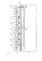
以下、本発明の実施形態について、図面を参照して説明する。図1は、本発明の第1の実施形態における固体撮像装置の概略構成を示した概観図である。第1の実施形態の固体撮像装置1は、複数の半導体基板を積層(接合)して構成する。図1において、固体撮像装置1は、第1の半導体基板11と、第2の半導体基板12とを、チップ接続部13によって接合している。 (First embodiment)
Hereinafter, embodiments of the present invention will be described with reference to the drawings. FIG. 1 is an overview diagram showing a schematic configuration of the solid-state imaging device according to the first embodiment of the present invention. The solid-state imaging device 1 according to the first embodiment is configured by stacking (joining) a plurality of semiconductor substrates. In FIG. 1, in the solid-state imaging device 1, a first semiconductor substrate 11 and a second semiconductor substrate 12 are joined by a chip connection unit 13.
以下、本発明の実施形態について、図面を参照して説明する。図1は、本発明の第1の実施形態における固体撮像装置の概略構成を示した概観図である。第1の実施形態の固体撮像装置1は、複数の半導体基板を積層(接合)して構成する。図1において、固体撮像装置1は、第1の半導体基板11と、第2の半導体基板12とを、チップ接続部13によって接合している。 (First embodiment)
Hereinafter, embodiments of the present invention will be described with reference to the drawings. FIG. 1 is an overview diagram showing a schematic configuration of the solid-state imaging device according to the first embodiment of the present invention. The solid-
固体撮像装置1は、固体撮像装置1の機能を実現するための回路を、第1の半導体基板11または第2の半導体基板12のいずれか一方の半導体基板上に形成する。固体撮像装置1の機能を実現するための回路は、入射してきた光(光線)を光電変換するフォトダイオードなどの光電変換素子、および光電変換素子が発生した電荷信号を読み出す読み出し回路を含む画素が二次元の行列状に複数配置された画素アレイ部、画素アレイ部内の画素を駆動するための駆動回路などがある。
The solid-state imaging device 1 forms a circuit for realizing the function of the solid-state imaging device 1 on either one of the first semiconductor substrate 11 and the second semiconductor substrate 12. A circuit for realizing the function of the solid-state imaging device 1 includes a pixel including a photoelectric conversion element such as a photodiode that photoelectrically converts incident light (light beam), and a readout circuit that reads a charge signal generated by the photoelectric conversion element. There are a plurality of pixel array units arranged in a two-dimensional matrix, a drive circuit for driving the pixels in the pixel array unit, and the like.
なお、固体撮像装置1の機能を実現するためのそれぞれの回路は、第1の半導体基板11または第2の半導体基板12のいずれか一方の半導体基板上に形成する構成のみではなく、第1の半導体基板11および第2の半導体基板12の両方の半導体基板上に形成する構成であってもよい。
Note that each circuit for realizing the function of the solid-state imaging device 1 is not only configured to be formed on one of the first semiconductor substrate 11 and the second semiconductor substrate 12 but also the first circuit. The semiconductor substrate 11 and the second semiconductor substrate 12 may be formed on both semiconductor substrates.
それぞれの半導体基板上に形成された固体撮像装置1の機能を実現するためのそれぞれの回路は、チップ接続部13によって電気的に接続する。そして、第1の半導体基板11に形成した回路と第2の半導体基板12に形成した回路とは、チップ接続部13を介して信号の送受信を行う。
Each circuit for realizing the function of the solid-state imaging device 1 formed on each semiconductor substrate is electrically connected by the chip connection unit 13. The circuit formed on the first semiconductor substrate 11 and the circuit formed on the second semiconductor substrate 12 transmit and receive signals via the chip connection portion 13.
チップ接続部13は、例えば、蒸着法、めっき法で作製されるマイクロバンプなどを用いる。なお、それぞれの半導体基板上に形成された固体撮像装置1の機能を実現するためのそれぞれの回路を接続する方法は、マイクロバンプを用いた方法に限定されるものではなく、例えば、シリコン貫通電極(TSV:Through-Silicon-Via)を用いた方法であってもよい。
The chip connection portion 13 uses, for example, a micro bump produced by a vapor deposition method or a plating method. In addition, the method of connecting each circuit for implement | achieving the function of the solid-state imaging device 1 formed on each semiconductor substrate is not limited to the method using a micro bump, For example, a silicon penetration electrode A method using (TSV: Through-Silicon-Via) may be used.
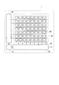
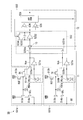
次に、第1の実施形態の固体撮像装置1の構成の一例について説明する。図2は、本発明の第1の実施形態における固体撮像装置1の概略構成を示したブロック図である。図2において、固体撮像装置1は、制御回路10と、垂直走査回路20と、水平走査回路30と、複数の画素50が配置された画素アレイ部40とを備えている。なお、図1に示した固体撮像装置1では、複数の画素50が、7行8列に2次元的に配置された画素アレイ部40の例を示している。
Next, an example of the configuration of the solid-state imaging device 1 according to the first embodiment will be described. FIG. 2 is a block diagram showing a schematic configuration of the solid-state imaging device 1 according to the first embodiment of the present invention. In FIG. 2, the solid-state imaging device 1 includes a control circuit 10, a vertical scanning circuit 20, a horizontal scanning circuit 30, and a pixel array unit 40 in which a plurality of pixels 50 are arranged. In the solid-state imaging device 1 illustrated in FIG. 1, an example of a pixel array unit 40 in which a plurality of pixels 50 are two-dimensionally arranged in 7 rows and 8 columns is illustrated.
制御回路10は、垂直走査回路20、水平走査回路30を制御する。
垂直走査回路20は、制御回路10からの制御に応じて、画素アレイ部40内のそれぞれの画素50を制御し、それぞれの画素50の画素信号を垂直信号線60に出力させる駆動回路である。垂直走査回路20は、画素50を駆動するための制御信号を、画素アレイ部40に備えた画素50の行ごとに出力する。 Thecontrol circuit 10 controls the vertical scanning circuit 20 and the horizontal scanning circuit 30.
Thevertical scanning circuit 20 is a drive circuit that controls each pixel 50 in the pixel array unit 40 in accordance with control from the control circuit 10 and outputs a pixel signal of each pixel 50 to the vertical signal line 60. The vertical scanning circuit 20 outputs a control signal for driving the pixels 50 for each row of the pixels 50 provided in the pixel array unit 40.
垂直走査回路20は、制御回路10からの制御に応じて、画素アレイ部40内のそれぞれの画素50を制御し、それぞれの画素50の画素信号を垂直信号線60に出力させる駆動回路である。垂直走査回路20は、画素50を駆動するための制御信号を、画素アレイ部40に備えた画素50の行ごとに出力する。 The
The
水平走査回路30は、画素アレイ部40に備えたそれぞれの画素50から行ごとに出力された画素信号を順次、固体撮像装置1の外部に出力させる駆動回路である。
The horizontal scanning circuit 30 is a drive circuit that sequentially outputs pixel signals output for each row from the respective pixels 50 provided in the pixel array unit 40 to the outside of the solid-state imaging device 1.
画素アレイ部40内に配置されたそれぞれの画素50は、入射してきた光(光線)を光電変換した電荷信号を発生させる。画素アレイ部40内に配置された画素50には、通常の撮影による電荷信号を発生させる構成の画素50と、動き検出のための電荷信号を発生させる構成の画素50とがある。
Each pixel 50 arranged in the pixel array unit 40 generates a charge signal obtained by photoelectrically converting incident light (light beam). The pixels 50 arranged in the pixel array unit 40 include a pixel 50 configured to generate a charge signal by normal photographing and a pixel 50 configured to generate a charge signal for motion detection.
通常の撮影による電荷信号を発生させる構成の画素50は、垂直走査回路20から入力された制御信号に応じたAPS(Active Pixel Sensor)読み出し(以下、「通常読み出し」という)によって、発生させた電荷信号に応じた画素信号を行ごとに、垂直信号線60に出力する。そして、垂直信号線60に出力されたそれぞれの行の画素信号は、水平走査回路30による制御に応じて、固体撮像装置1の外部に出力される。すなわち、通常の撮影による電荷信号を発生させる構成の画素50の画素信号は、通常の撮影におけるフレームごとに、固体撮像装置1の外部に出力される。なお、以下の説明においては、通常の撮影による電荷信号を発生させる構成の画素50、つまり、通常の撮影の画素信号を出力する画素50を「通常画素51」という。
The pixel 50 configured to generate a charge signal by normal photographing is generated by APS (Active Pixel Sensor) reading (hereinafter referred to as “normal reading”) in accordance with a control signal input from the vertical scanning circuit 20. A pixel signal corresponding to the signal is output to the vertical signal line 60 for each row. Then, the pixel signals of each row output to the vertical signal line 60 are output to the outside of the solid-state imaging device 1 according to control by the horizontal scanning circuit 30. That is, the pixel signal of the pixel 50 configured to generate a charge signal by normal shooting is output to the outside of the solid-state imaging device 1 for each frame in normal shooting. In the following description, a pixel 50 configured to generate a charge signal by normal photographing, that is, a pixel 50 that outputs a normal photographing pixel signal is referred to as a “normal pixel 51”.
また、動き検出のための電荷信号を発生させる構成の画素50は、AER(Address Event Representation)読み出し(以下、「動き検出読み出し」という)によって、電荷信号の時間的な変化および変化した方向を表すパルス信号を、垂直走査回路20による通常画素51の駆動とは同期せずに、つまり、非同期で出力する。このとき、動き検出のための電荷信号を発生させる構成の画素50は、画素50自身の位置を表すアドレス情報をパルス信号に付加し、画素信号として出力する。なお、以下の説明においては、動き検出のための電荷信号を発生させる構成の画素50、つまり、動き検出の画素信号を出力する画素50を「動き検出画素52」という。
Further, the pixel 50 configured to generate a charge signal for motion detection represents a temporal change and a changed direction of the charge signal by AER (Address Event Representation) reading (hereinafter referred to as “motion detection reading”). The pulse signal is output without being synchronized with the driving of the normal pixel 51 by the vertical scanning circuit 20, that is, asynchronously. At this time, the pixel 50 configured to generate a charge signal for motion detection adds address information indicating the position of the pixel 50 itself to the pulse signal and outputs it as a pixel signal. In the following description, a pixel 50 configured to generate a charge signal for motion detection, that is, a pixel 50 that outputs a pixel signal for motion detection is referred to as a “motion detection pixel 52”.
通常画素51および動き検出画素52のそれぞれを構成する回路要素は、第1の半導体基板11または第2の半導体基板12のいずれか一方または両方の半導体基板に形成し、チップ接続部13によって画素アレイ部40内で接続する。
Circuit elements constituting each of the normal pixel 51 and the motion detection pixel 52 are formed on one or both of the first semiconductor substrate 11 and the second semiconductor substrate 12, and the pixel array is formed by the chip connection unit 13. The connection is made within the unit 40.
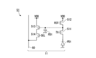
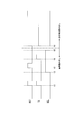
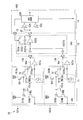
次に、第1の実施形態の固体撮像装置1において画素アレイ部40内に配置する通常画素51および動き検出画素52の構成について説明する。図3Aおよび図3Bは、本発明の第1の実施形態の固体撮像装置1における画素50(通常画素51および動き検出画素52)の構成の一例を示した回路図である。図3Aには、固体撮像装置1の画素アレイ部40内に配置する通常画素51の構成の一例を示し、図3Bには、固体撮像装置1の画素アレイ部40内に配置する動き検出画素52の構成の一例を示している。
Next, the configuration of the normal pixels 51 and the motion detection pixels 52 arranged in the pixel array unit 40 in the solid-state imaging device 1 of the first embodiment will be described. 3A and 3B are circuit diagrams illustrating an example of the configuration of the pixel 50 (the normal pixel 51 and the motion detection pixel 52) in the solid-state imaging device 1 according to the first embodiment of the present invention. FIG. 3A shows an example of the configuration of the normal pixel 51 arranged in the pixel array unit 40 of the solid-state imaging device 1, and FIG. 3B shows the motion detection pixel 52 arranged in the pixel array unit 40 of the solid-state imaging device 1. An example of the configuration is shown.
まず、図3Aを用いて、通常画素51の構成を説明する。図3Aにおいて、通常画素51は、光電変換素子PD1と、電荷転送トランジスタ511、画素リセットトランジスタ512、増幅トランジスタ513、および選択トランジスタ514とを備えている。なお、図3Aにおいては、通常画素51に備えた増幅トランジスタ513のゲート端子に接続されたノードに付随する容量であるノード容量FD1を、通常画素51の回路要素としてキャパシタの記号で示している。
First, the configuration of the normal pixel 51 will be described with reference to FIG. 3A. 3A, the normal pixel 51 includes a photoelectric conversion element PD1, a charge transfer transistor 511, a pixel reset transistor 512, an amplification transistor 513, and a selection transistor 514. In FIG. 3A, a node capacitance FD1, which is a capacitance associated with a node connected to the gate terminal of the amplification transistor 513 provided in the normal pixel 51, is indicated by a capacitor symbol as a circuit element of the normal pixel 51.
通常画素51においては、電荷転送トランジスタ511、画素リセットトランジスタ512、増幅トランジスタ513、および選択トランジスタ514と、ノード容量FD1とで、光電変換素子PD1が発生させた電荷信号に応じた画素信号を読み出す読み出し回路を構成している。固体撮像装置1では、光電変換素子PD1と読み出し回路とを、第1の半導体基板11に形成する。
In the normal pixel 51, the charge transfer transistor 511, the pixel reset transistor 512, the amplification transistor 513, the selection transistor 514, and the node capacitor FD1 read out a pixel signal corresponding to the charge signal generated by the photoelectric conversion element PD1. The circuit is configured. In the solid-state imaging device 1, the photoelectric conversion element PD <b> 1 and the readout circuit are formed on the first semiconductor substrate 11.
光電変換素子PD1は、入射してきた光(光線)を光電変換して電荷信号を発生させ、発生させた電荷信号を蓄積するフォトダイオードである。
The photoelectric conversion element PD1 is a photodiode that photoelectrically converts incident light (light beam) to generate a charge signal and accumulates the generated charge signal.
電荷転送トランジスタ511は、垂直走査回路20から入力された制御信号TXに応じて、光電変換素子PD1が発生して蓄積した電荷信号を、増幅トランジスタ513のゲート端子に転送する。これにより、電荷転送トランジスタ511によって転送された電荷信号が、ノード容量FD1に蓄積される。
The charge transfer transistor 511 transfers the charge signal generated and accumulated by the photoelectric conversion element PD1 to the gate terminal of the amplification transistor 513 in accordance with the control signal TX input from the vertical scanning circuit 20. As a result, the charge signal transferred by the charge transfer transistor 511 is accumulated in the node capacitor FD1.
増幅トランジスタ513は、ゲート端子に転送された電荷信号、すなわち、ノード容量FD1に蓄積された電荷信号に応じた信号電圧を、選択トランジスタ514に出力する。
The amplification transistor 513 outputs to the selection transistor 514 a signal voltage corresponding to the charge signal transferred to the gate terminal, that is, the charge signal stored in the node capacitor FD1.
画素リセットトランジスタ512は、垂直走査回路20から入力された制御信号RSTに応じて、通常画素51内の電荷信号を、電源電圧VDDにリセットする。
The pixel reset transistor 512 resets the charge signal in the normal pixel 51 to the power supply voltage VDD in accordance with the control signal RST input from the vertical scanning circuit 20.
選択トランジスタ514は、垂直走査回路20から入力された制御信号SELに応じて、増幅トランジスタ513から出力される信号電圧を、通常画素51の画素信号として垂直信号線60に出力する。これにより、通常画素51に備えた光電変換素子PD1が発生した電荷信号に応じた画素信号が、垂直信号線60に読み出される。
The selection transistor 514 outputs the signal voltage output from the amplification transistor 513 to the vertical signal line 60 as the pixel signal of the normal pixel 51 in accordance with the control signal SEL input from the vertical scanning circuit 20. As a result, a pixel signal corresponding to the charge signal generated by the photoelectric conversion element PD <b> 1 provided in the normal pixel 51 is read out to the vertical signal line 60.
このような構成によって、通常画素51では、光電変換素子PD1が入射した光を光電変換した電荷信号に応じたそれぞれの信号電圧を、画素信号として垂直信号線60に読み出す。
With such a configuration, in the normal pixel 51, each signal voltage corresponding to the charge signal obtained by photoelectrically converting the light incident on the photoelectric conversion element PD1 is read out to the vertical signal line 60 as a pixel signal.
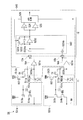
続いて、図3Bを用いて、動き検出画素52の構成を説明する。図3Bにおいて、動き検出画素52は、光電変換素子PD2と、アンプ521と、バイアストランジスタ522と、スイッチトキャパシタアンプ回路523と、スレッショルドアンプ524およびスレッショルドアンプ525と、AER回路526とを備えている。また、スイッチトキャパシタアンプ回路523は、キャパシタ5231と、アンプ5232と、キャパシタ5233と、スイッチ5234とを備えている。
Subsequently, the configuration of the motion detection pixel 52 will be described with reference to FIG. 3B. 3B, the motion detection pixel 52 includes a photoelectric conversion element PD2, an amplifier 521, a bias transistor 522, a switched capacitor amplifier circuit 523, a threshold amplifier 524, a threshold amplifier 525, and an AER circuit 526. The switched capacitor amplifier circuit 523 includes a capacitor 5231, an amplifier 5232, a capacitor 5233, and a switch 5234.
動き検出画素52においては、アンプ521およびバイアストランジスタ522で、光電変換素子PD2が発生させた電荷信号を出力する出力回路を構成している。また、動き検出画素52においては、スイッチトキャパシタアンプ回路523、スレッショルドアンプ524、スレッショルドアンプ525、およびAER回路526で、光電変換素子PD2が発生させた電荷信号を読み出す読み出し回路を構成している。固体撮像装置1では、光電変換素子PD2および出力回路を第1の半導体基板11に形成し、読み出し回路を第2の半導体基板12に形成する。
In the motion detection pixel 52, an amplifier 521 and a bias transistor 522 constitute an output circuit that outputs a charge signal generated by the photoelectric conversion element PD2. In the motion detection pixel 52, the switched capacitor amplifier circuit 523, the threshold amplifier 524, the threshold amplifier 525, and the AER circuit 526 form a readout circuit that reads the charge signal generated by the photoelectric conversion element PD2. In the solid-state imaging device 1, the photoelectric conversion element PD <b> 2 and the output circuit are formed on the first semiconductor substrate 11, and the readout circuit is formed on the second semiconductor substrate 12.
光電変換素子PD2は、通常画素51に備えた光電変換素子PD1と同様に、入射してきた光(光線)を光電変換して電荷信号を発生させ、発生させた電荷信号を蓄積するフォトダイオードである。光電変換素子PD2は、発生させた電荷信号を逐次、アンプ521に出力する。
Similar to the photoelectric conversion element PD1 provided in the normal pixel 51, the photoelectric conversion element PD2 is a photodiode that photoelectrically converts incident light (light rays) to generate a charge signal and accumulates the generated charge signal. . The photoelectric conversion element PD2 sequentially outputs the generated charge signal to the amplifier 521.
アンプ521は、光電変換素子PD2が発生して出力した電荷信号を、増幅する。アンプ521は、増幅した電荷信号を、チップ接続部13を介してスイッチトキャパシタアンプ回路523に出力する。これにより、光電変換素子PD2が発生する電荷信号の変化が、スイッチトキャパシタアンプ回路523に入力される。また、アンプ521は、増幅した電荷信号を、バイアストランジスタ522のゲート端子に転送する。
The amplifier 521 amplifies the charge signal generated and output by the photoelectric conversion element PD2. The amplifier 521 outputs the amplified charge signal to the switched capacitor amplifier circuit 523 via the chip connection unit 13. As a result, a change in the charge signal generated by the photoelectric conversion element PD2 is input to the switched capacitor amplifier circuit 523. In addition, the amplifier 521 transfers the amplified charge signal to the gate terminal of the bias transistor 522.
バイアストランジスタ522は、ゲート端子に転送された電荷信号に応じて光電変換素子PD2に流れる電流が一定の電流になるように制御する。これにより、光電変換素子PD2が発生する電荷信号が変化した場合、電荷信号の大きさが逐次、変化した後の大きさで安定する。つまり、光電変換素子PD2の出力がクリップされる。
The bias transistor 522 controls the current flowing through the photoelectric conversion element PD2 to be a constant current according to the charge signal transferred to the gate terminal. Thus, when the charge signal generated by the photoelectric conversion element PD2 changes, the magnitude of the charge signal is stabilized at the magnitude after the change. That is, the output of the photoelectric conversion element PD2 is clipped.
スイッチトキャパシタアンプ回路523は、アンプ521からチップ接続部13を介して入力された電荷信号の変化、つまり、光電変換素子PD2が発生する電荷信号の増減を、予め定めた電圧の範囲の電圧信号に変換し、スレッショルドアンプ524およびスレッショルドアンプ525のそれぞれに出力する。また、スイッチトキャパシタアンプ回路523の動作は、AER回路526によってリセットされる。
The switched capacitor amplifier circuit 523 converts the change in the charge signal input from the amplifier 521 via the chip connection unit 13, that is, the increase or decrease in the charge signal generated by the photoelectric conversion element PD2 into a voltage signal in a predetermined voltage range. The data is converted and output to each of the threshold amplifier 524 and the threshold amplifier 525. The operation of the switched capacitor amplifier circuit 523 is reset by the AER circuit 526.
より具体的には、アンプ521からチップ接続部13を介して入力された電荷信号は、キャパシタ5231の第1の端子に入力されて蓄積される。これにより、キャパシタ5231の第2の端子から、蓄積した電荷信号に応じた電圧の電圧信号が出力されてアンプ5232に出力される。
More specifically, the charge signal input from the amplifier 521 via the chip connection unit 13 is input to the first terminal of the capacitor 5231 and stored. Accordingly, a voltage signal having a voltage corresponding to the accumulated charge signal is output from the second terminal of the capacitor 5231 and output to the amplifier 5232.
アンプ5232は、入力された電圧信号の電圧を増幅し、増幅した電圧信号を、スイッチトキャパシタアンプ回路523の出力としてスレッショルドアンプ524およびスレッショルドアンプ525のそれぞれにて出力する。また、アンプ5232が出力した電圧信号は、キャパシタ5233の第1の端子に入力されて蓄積される。これにより、キャパシタ5233の第2の端子から、蓄積した電圧信号に応じた電圧の信号が、フィードバック信号としてアンプ5232に出力される。そして、アンプ5232は、フィードバック信号の電圧に応じた一定の電圧の電圧信号を出力し続ける。つまり、アンプ5232は、アンプ521からチップ接続部13を介してスイッチトキャパシタアンプ回路523に入力された電荷信号に応じた電圧の電圧信号を、スレッショルドアンプ524およびスレッショルドアンプ525のそれぞれに出力し続ける。ここで、アンプ5232がスレッショルドアンプ524およびスレッショルドアンプ525のそれぞれに出力する電圧信号は、光電変換素子PD2が発生する電荷信号が増減した大きさを表す電圧の信号である。
The amplifier 5232 amplifies the voltage of the input voltage signal, and outputs the amplified voltage signal as an output of the switched capacitor amplifier circuit 523 in each of the threshold amplifier 524 and the threshold amplifier 525. The voltage signal output from the amplifier 5232 is input to the first terminal of the capacitor 5233 and accumulated. Thus, a voltage signal corresponding to the accumulated voltage signal is output from the second terminal of the capacitor 5233 to the amplifier 5232 as a feedback signal. The amplifier 5232 continues to output a voltage signal having a constant voltage corresponding to the voltage of the feedback signal. That is, the amplifier 5232 continues to output a voltage signal having a voltage corresponding to the charge signal input from the amplifier 521 to the switched capacitor amplifier circuit 523 via the chip connection unit 13 to each of the threshold amplifier 524 and the threshold amplifier 525. Here, the voltage signal output from the amplifier 5232 to each of the threshold amplifier 524 and the threshold amplifier 525 is a voltage signal indicating the magnitude of increase or decrease in the charge signal generated by the photoelectric conversion element PD2.
また、アンプ5232の出力端子(キャパシタ5233の第1の端子でもある)は、スイッチ5234の第1の端子に接続し、アンプ5232の入力端子(キャパシタ5233の第2の端子でもある)は、スイッチ5234の第2の端子に接続している。そして、スイッチ5234は、AER回路526から出力され、制御端子に入力されるリセット信号によって短絡と開放とが制御される。スイッチ5234は、AER回路526から出力されたリセット信号によって短絡するように制御されると、第1の端子と第2の端子とを短絡する。これにより、キャパシタ5233の両方の端子が短絡されて、キャパシタ5233の両方の端子の電圧が同じ電圧なってリセットされると共に、アンプ5232による電圧信号の増幅動作もリセットされる。
The output terminal of the amplifier 5232 (which is also the first terminal of the capacitor 5233) is connected to the first terminal of the switch 5234, and the input terminal of the amplifier 5232 (which is also the second terminal of the capacitor 5233) is the switch. 5234 is connected to the second terminal. The switch 5234 is output from the AER circuit 526, and the short circuit and the open circuit are controlled by the reset signal input to the control terminal. When the switch 5234 is controlled to be short-circuited by the reset signal output from the AER circuit 526, the switch 5234 short-circuits the first terminal and the second terminal. Accordingly, both terminals of the capacitor 5233 are short-circuited, the voltages of both terminals of the capacitor 5233 are reset to the same voltage, and the amplification operation of the voltage signal by the amplifier 5232 is also reset.
なお、図3Bには、キャパシタ5231、アンプ5232、キャパシタ5233、およびスイッチ5234によって構成したスイッチトキャパシタアンプ回路523を示したが、スイッチトキャパシタアンプ回路523の構成は、図3Bに示した構成に限定されるものではない。
3B shows the switched capacitor amplifier circuit 523 configured by the capacitor 5231, the amplifier 5232, the capacitor 5233, and the switch 5234. However, the configuration of the switched capacitor amplifier circuit 523 is limited to the configuration illustrated in FIG. 3B. It is not something.
スレッショルドアンプ524およびスレッショルドアンプ525のそれぞれは、スイッチトキャパシタアンプ回路523内のアンプ5232から入力された電圧信号の電圧の変化と、変化した方向とを検出する。
Each of the threshold amplifier 524 and the threshold amplifier 525 detects a change in the voltage of the voltage signal input from the amplifier 5232 in the switched capacitor amplifier circuit 523 and the changed direction.
より具体的には、スレッショルドアンプ524およびスレッショルドアンプ525のそれぞれは、スイッチトキャパシタアンプ回路523内のアンプ5232から入力された電圧信号の電圧と、予め定めた閾値電圧(スレッショルド電圧)とを比較する。そして、スレッショルドアンプ524およびスレッショルドアンプ525のそれぞれは、入力された電圧信号の電圧がスレッショルド電圧を超えた場合に、スレッショルド電圧を超えた変化があることを表すイベント信号を、AER回路526に出力する。
More specifically, each of the threshold amplifier 524 and the threshold amplifier 525 compares the voltage of the voltage signal input from the amplifier 5232 in the switched capacitor amplifier circuit 523 with a predetermined threshold voltage (threshold voltage). Each of the threshold amplifier 524 and the threshold amplifier 525 outputs an event signal indicating that there is a change exceeding the threshold voltage to the AER circuit 526 when the voltage of the input voltage signal exceeds the threshold voltage. .
なお、スレッショルドアンプ524およびスレッショルドアンプ525のそれぞれには、予め定めた正方向の電圧または負方向の電圧のいずれか一方の電圧が、スレッショルド電圧として設定されている。図3Bに示した構成では、スレッショルドアンプ524に、予め定めた電圧値の正方向の電圧がスレッショルド電圧として設定され、スレッショルドアンプ525に、予め定めた電圧値の負方向の電圧がスレッショルド電圧として設定されている。このため、スレッショルドアンプ524は、アンプ5232から入力された電圧信号の電圧が、正方向のスレッショルド電圧よりも多く正方向(増加する方向)に変化したか否かを検出する。また、スレッショルドアンプ525は、アンプ5232から入力された電圧信号の電圧が、負方向のスレッショルド電圧よりも多く負方向(減少する方向)に変化したか否かを検出する。
Note that, in each of the threshold amplifier 524 and the threshold amplifier 525, either a predetermined positive voltage or negative voltage is set as the threshold voltage. In the configuration shown in FIG. 3B, a positive voltage having a predetermined voltage value is set as a threshold voltage in the threshold amplifier 524, and a negative voltage having a predetermined voltage value is set as a threshold voltage in the threshold amplifier 525. Has been. Therefore, the threshold amplifier 524 detects whether or not the voltage of the voltage signal input from the amplifier 5232 has changed in the positive direction (increase direction) more than the threshold voltage in the positive direction. The threshold amplifier 525 detects whether the voltage of the voltage signal input from the amplifier 5232 has changed in the negative direction (decreasing direction) more than the threshold voltage in the negative direction.
このように、スレッショルドアンプ524とスレッショルドアンプ525との構成によって、スイッチトキャパシタアンプ回路523によって予め定めた電圧の範囲に変換された電圧信号のスレッショルド電圧を超える変化および変化した方向とを検出する。これは、光電変換素子PD2が発生した電荷信号の予め定めた閾値を超えた変化および変化した方向を検出することに相当する。そして、スレッショルドアンプ524およびスレッショルドアンプ525のそれぞれがAER回路526に出力するイベント信号が、光電変換素子PD2が発生した電荷信号の変化と変化した方向(正方向または負方向)とを表している。つまり、スレッショルドアンプ524がイベント信号を出力した場合には、光電変換素子PD2が発生した電荷信号に、正方向の予め定めた閾値を超える変化があったことを表し、スレッショルドアンプ525がイベント信号を出力した場合には、光電変換素子PD2が発生した電荷信号に、負方向の予め定めた閾値を超える変化があったことを表している。
As described above, the configuration of the threshold amplifier 524 and the threshold amplifier 525 detects the change exceeding the threshold voltage of the voltage signal converted into the predetermined voltage range by the switched capacitor amplifier circuit 523 and the changed direction. This corresponds to detecting a change and a changed direction of the charge signal generated by the photoelectric conversion element PD2 exceeding a predetermined threshold. The event signals output from the threshold amplifier 524 and the threshold amplifier 525 to the AER circuit 526 represent the change of the charge signal generated by the photoelectric conversion element PD2 and the changed direction (positive direction or negative direction). That is, when the threshold amplifier 524 outputs an event signal, it indicates that the charge signal generated by the photoelectric conversion element PD2 has changed beyond a predetermined threshold value in the positive direction, and the threshold amplifier 525 outputs the event signal. When output, it indicates that the charge signal generated by the photoelectric conversion element PD2 has changed beyond a predetermined threshold value in the negative direction.
なお、図3Bに示した構成では、スイッチトキャパシタアンプ回路523と、スレッショルドアンプ524およびスレッショルドアンプ525との構成によって、光電変換素子PD2が発生した電荷信号の時間的な変化を検出している。しかし、光電変換素子PD2が発生した電荷信号の時間的な変化を検出する構成は、図3Bに示した構成に限定されるものではない。例えば、スレッショルドアンプ524とスレッショルドアンプ525とによって、光電変換素子PD2が発生した電荷信号の時間的な変化を検出する構成にしてもよい。
Note that in the configuration shown in FIG. 3B, the temporal change of the charge signal generated by the photoelectric conversion element PD2 is detected by the configuration of the switched capacitor amplifier circuit 523, the threshold amplifier 524, and the threshold amplifier 525. However, the configuration for detecting the temporal change of the charge signal generated by the photoelectric conversion element PD2 is not limited to the configuration shown in FIG. 3B. For example, the threshold amplifier 524 and the threshold amplifier 525 may be configured to detect temporal changes in the charge signal generated by the photoelectric conversion element PD2.
AER回路526は、スレッショルドアンプ524とスレッショルドアンプ525とのそれぞれから入力されたイベント信号に基づいて、光電変換素子PD2が発生させた電荷信号が正方向または負方向のいずれの方向に変化したか、つまり、電荷信号の大きさの増減を判定する。そして、AER回路526は、判定した結果を表すパルス信号を生成する。例えば、光電変換素子PD2が発生させた電荷信号が正方向(増加する方向)に変化した場合に正方向のパルス信号を生成し、光電変換素子PD2が発生させた電荷信号が負方向(減少する方向)に変化した場合に負方向のパルス信号を生成する。そして、AER回路526は、生成したパルス信号に、動き検出画素52自身の位置を表すアドレス情報を付加し、画素信号として出力する。なお、以下の説明においては、通常画素51が出力する画素信号と区別するため、AER回路526、すなわち、動き検出画素52が出力する画素信号を、「イベント画素信号」という。
The AER circuit 526 determines whether the charge signal generated by the photoelectric conversion element PD2 changes in the positive direction or the negative direction based on the event signals input from the threshold amplifier 524 and the threshold amplifier 525, respectively. That is, the increase / decrease in the magnitude of the charge signal is determined. Then, the AER circuit 526 generates a pulse signal representing the determined result. For example, when the charge signal generated by the photoelectric conversion element PD2 changes in the positive direction (increase direction), a positive pulse signal is generated, and the charge signal generated by the photoelectric conversion element PD2 decreases in the negative direction (decreases). Direction), a negative pulse signal is generated. The AER circuit 526 adds address information indicating the position of the motion detection pixel 52 itself to the generated pulse signal, and outputs it as a pixel signal. In the following description, the pixel signal output from the AER circuit 526, that is, the motion detection pixel 52, is referred to as an “event pixel signal” in order to distinguish from the pixel signal output from the normal pixel 51.
このような構成によって、動き検出画素52では、光電変換素子PD2が入射した光を光電変換した電荷信号の変化とその変化した方向とを検出し、検出した情報と、動き検出画素52の位置を表すアドレス情報とを、動き検出画素52ごとに出力する。
With such a configuration, the motion detection pixel 52 detects a change in the charge signal obtained by photoelectric conversion of the light incident on the photoelectric conversion element PD2 and its changed direction, and detects the detected information and the position of the motion detection pixel 52. The address information to be expressed is output for each motion detection pixel 52.
なお、動き検出画素52が出力するイベント画素信号は、上述したように、それぞれの動き検出画素52ごとに出力する構成であってもよいが、それぞれの動き検出画素52がイベント画素信号を出力する構成は限定しない。例えば、それぞれの動き検出画素52が、水平走査回路30を介してイベント画素信号を出力する構成であってもよい。また、画素アレイ部40内の予め定めた範囲ごとにまとめた形式でイベント画素信号を出力する構成であってもよい。
The event pixel signal output from the motion detection pixel 52 may be output for each motion detection pixel 52 as described above, but each motion detection pixel 52 outputs an event pixel signal. The configuration is not limited. For example, each motion detection pixel 52 may be configured to output an event pixel signal via the horizontal scanning circuit 30. Moreover, the structure which outputs an event pixel signal in the form put together for every predetermined range in the pixel array part 40 may be sufficient.
また、動き検出画素52では、AER回路526が、生成したパルス信号にアドレス情報を付加することによって、イベント画素信号として出力する構成を示したが、パルス信号にアドレス情報を付加する構成は、AER回路526に限定されるものではない。例えば、固体撮像装置1に備えた不図示の構成要素が、それぞれの動き検出画素52に備えたAER回路526が出力したパルス信号に、パルス信号を出力した動き検出画素52の位置を表すアドレス情報を付加し、イベント画素信号として出力する構成であってもよい。
In the motion detection pixel 52, the AER circuit 526 adds the address information to the generated pulse signal and outputs the event pixel signal. However, the configuration for adding the address information to the pulse signal is the AER It is not limited to the circuit 526. For example, the address information indicating the position of the motion detection pixel 52 that outputs the pulse signal to the pulse signal output from the AER circuit 526 provided in each motion detection pixel 52 by a component (not shown) included in the solid-state imaging device 1. May be added and output as an event pixel signal.
また、動き検出画素52では、スイッチトキャパシタアンプ回路523によって、光電変換素子PD2が発生した電荷信号を増幅してから予め定めた電圧の範囲の電圧信号に変換する構成を示した。しかし、動き検出画素52において、光電変換素子PD2が発生した電荷信号を予め定めた電圧の範囲の電圧信号に変換する構成は、スイッチトキャパシタアンプ回路523による構成に限定しない。例えば、動き検出画素52を、スイッチトキャパシタアンプ回路523に備えたアンプ5232を備えない構成、いわゆる、スイッチトキャパシタ回路によって、光電変換素子PD2が発生した電荷信号を予め定めた電圧の範囲の電圧信号に変換する構成にしてもよい。この場合、動き検出画素52は、スイッチトキャパシタ回路と、スレッショルドアンプ524およびスレッショルドアンプ525との構成によって、光電変換素子PD2が発生した電荷信号の時間的な変化を検出してもよい。
In the motion detection pixel 52, the switched capacitor amplifier circuit 523 amplifies the charge signal generated by the photoelectric conversion element PD2 and then converts the amplified signal into a voltage signal in a predetermined voltage range. However, in the motion detection pixel 52, the configuration for converting the charge signal generated by the photoelectric conversion element PD2 into a voltage signal in a predetermined voltage range is not limited to the configuration using the switched capacitor amplifier circuit 523. For example, the motion detection pixel 52 is configured so as not to include the amplifier 5232 included in the switched capacitor amplifier circuit 523, that is, a so-called switched capacitor circuit, and the charge signal generated by the photoelectric conversion element PD2 is converted into a voltage signal in a predetermined voltage range. You may make it the structure to convert. In this case, the motion detection pixel 52 may detect a temporal change in the charge signal generated by the photoelectric conversion element PD2 by the configuration of the switched capacitor circuit, the threshold amplifier 524, and the threshold amplifier 525.
(第1の配置例)
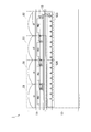
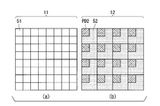
次に、第1の実施形態の固体撮像装置1における画素アレイ部40内の通常画素51および動き検出画素52の配置の一例について説明する。図4は、本発明の第1の実施形態の固体撮像装置1における画素50(通常画素51および動き検出画素52)の配置の一例(第1の配置例)を模式的に示した図である。図4には、固体撮像装置1を構成するそれぞれの半導体基板に形成する画素アレイ部40内の通常画素51および動き検出画素52の配置の一例を示している。 (First arrangement example)
Next, an example of the arrangement of thenormal pixels 51 and the motion detection pixels 52 in the pixel array unit 40 in the solid-state imaging device 1 of the first embodiment will be described. FIG. 4 is a diagram schematically illustrating an example (first arrangement example) of the arrangement of the pixels 50 (the normal pixels 51 and the motion detection pixels 52) in the solid-state imaging device 1 according to the first embodiment of the present invention. . FIG. 4 shows an example of the arrangement of the normal pixels 51 and the motion detection pixels 52 in the pixel array unit 40 formed on each semiconductor substrate constituting the solid-state imaging device 1.
次に、第1の実施形態の固体撮像装置1における画素アレイ部40内の通常画素51および動き検出画素52の配置の一例について説明する。図4は、本発明の第1の実施形態の固体撮像装置1における画素50(通常画素51および動き検出画素52)の配置の一例(第1の配置例)を模式的に示した図である。図4には、固体撮像装置1を構成するそれぞれの半導体基板に形成する画素アレイ部40内の通常画素51および動き検出画素52の配置の一例を示している。 (First arrangement example)
Next, an example of the arrangement of the
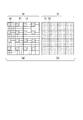
固体撮像装置1における画素の第1の配置例では、画素50、つまり、通常画素51と動き検出画素52とを平面状に配置する。このとき、固体撮像装置1では、上述したように、通常画素51を第1の半導体基板11に形成し、動き検出画素52を第1の半導体基板11と第2の半導体基板12とに分けて形成する。図4の(a)には、固体撮像装置1を構成する第1の半導体基板11の画素アレイ部40の領域内に画素50(通常画素51および動き検出画素52)を配置した一例を示している。また、図4の(b)には、固体撮像装置1を構成する第2の半導体基板12の画素アレイ部40の領域内に動き検出画素52を配置した一例を示している。
In the first arrangement example of the pixels in the solid-state imaging device 1, the pixels 50, that is, the normal pixels 51 and the motion detection pixels 52 are arranged in a planar shape. At this time, in the solid-state imaging device 1, as described above, the normal pixels 51 are formed on the first semiconductor substrate 11, and the motion detection pixels 52 are divided into the first semiconductor substrate 11 and the second semiconductor substrate 12. Form. 4A shows an example in which the pixels 50 (the normal pixels 51 and the motion detection pixels 52) are arranged in the region of the pixel array unit 40 of the first semiconductor substrate 11 constituting the solid-state imaging device 1. FIG. Yes. FIG. 4B shows an example in which the motion detection pixels 52 are arranged in the region of the pixel array section 40 of the second semiconductor substrate 12 constituting the solid-state imaging device 1.
より具体的には、図4の(a)に示したように、第1の半導体基板11の画素アレイ部40の平面の領域には、通常画素51と動き検出画素52の光電変換素子PD2および出力回路とを、行方向および列方向に周期的に配置する。このとき、通常画素51は、図4の(a)に示したように、動き検出画素52よりも多く配置する。なお、図4の(a)では、通常画素51と動き検出画素52の光電変換素子PD2および出力回路とを、交互に配置している。
More specifically, as shown in FIG. 4A, the photoelectric conversion element PD <b> 2 of the normal pixel 51 and the motion detection pixel 52, and the planar area of the pixel array unit 40 of the first semiconductor substrate 11. The output circuit is periodically arranged in the row direction and the column direction. At this time, the normal pixels 51 are arranged more than the motion detection pixels 52 as shown in FIG. In FIG. 4A, the photoelectric conversion elements PD2 and output circuits of the normal pixels 51 and the motion detection pixels 52 are alternately arranged.
また、図4の(b)に示したように、第2の半導体基板12の画素アレイ部40の平面の領域には、第1の半導体基板11に配置した動き検出画素52の光電変換素子PD2および出力回路に対応する動き検出画素52の読み出し回路を配置する。このとき、動き検出画素52の読み出し回路は、図4の(b)に示したように、第1の半導体基板11に配置した通常画素51に対応する第2の半導体基板12の画素アレイ部40の平面の領域を含めて形成する。つまり、固体撮像装置1では、通常画素51よりも多くの回路要素から構成されるため形成する際に多くの領域を必要とする動き検出画素52を、通常画素51を形成するために使用していない第2の半導体基板12の領域を利用して形成する。より具体的には、通常画素51に光が入射する側の面と反対側の面に積層された第2の半導体基板12において、第1の半導体基板11に形成された通常画素51の領域と重複している領域を含めて動き検出画素52の読み出し回路を形成する。そして、図4の(a)および図4の(b)に示したように、第1の半導体基板11に形成した出力回路と、第2の半導体基板12に形成した読み出し回路とを、チップ接続部13によって電気的に接続する。
Further, as shown in FIG. 4B, the photoelectric conversion element PD <b> 2 of the motion detection pixel 52 disposed on the first semiconductor substrate 11 is located in a planar region of the pixel array unit 40 of the second semiconductor substrate 12. A readout circuit for the motion detection pixel 52 corresponding to the output circuit is arranged. At this time, as shown in FIG. 4B, the readout circuit of the motion detection pixel 52 is a pixel array unit 40 of the second semiconductor substrate 12 corresponding to the normal pixel 51 arranged on the first semiconductor substrate 11. It is formed including the planar area. That is, in the solid-state imaging device 1, the motion detection pixel 52 that requires a large area when forming because it is composed of more circuit elements than the normal pixel 51 is used to form the normal pixel 51. It is formed using the region of the second semiconductor substrate 12 that is not present. More specifically, in the second semiconductor substrate 12 stacked on the surface opposite to the surface on which light is incident on the normal pixel 51, the region of the normal pixel 51 formed on the first semiconductor substrate 11 A readout circuit for the motion detection pixel 52 is formed including the overlapping region. Then, as shown in FIGS. 4A and 4B, the output circuit formed on the first semiconductor substrate 11 and the read circuit formed on the second semiconductor substrate 12 are connected to each other in a chip connection. Electrical connection is made by the section 13.
ここで、第1の実施形態の固体撮像装置1の構造について説明する。図5は、本発明の第1の実施形態の固体撮像装置1の構造の一例を示した断面図である。図5には、固体撮像装置1において通常画素51と動き検出画素52とが第1の配置例のように配置されている場合における画素アレイ部40の一部の縦構造を示している。より具体的には、第1の半導体基板11に形成された3個の通常画素51と、第1の半導体基板11および第2の半導体基板12に形成された1個の動き検出画素52との縦構造を示している。
Here, the structure of the solid-state imaging device 1 of the first embodiment will be described. FIG. 5 is a cross-sectional view showing an example of the structure of the solid-state imaging device 1 according to the first embodiment of the present invention. FIG. 5 shows a partial vertical structure of the pixel array unit 40 in the case where the normal pixels 51 and the motion detection pixels 52 are arranged as in the first arrangement example in the solid-state imaging device 1. More specifically, there are three normal pixels 51 formed on the first semiconductor substrate 11 and one motion detection pixel 52 formed on the first semiconductor substrate 11 and the second semiconductor substrate 12. The vertical structure is shown.
上述したように、固体撮像装置1では、動き検出画素52の読み出し回路を、第1の半導体基板11に形成された通常画素51の領域と重複している領域を含めた第2の半導体基板12の領域に形成する。図5には、第2の半導体基板12内に形成する動き検出画素52の読み出し回路に備えたスイッチトキャパシタアンプ回路523と、AER回路526とを形成している状態を示している。
As described above, in the solid-state imaging device 1, the second semiconductor substrate 12 including the region where the readout circuit of the motion detection pixel 52 overlaps the region of the normal pixel 51 formed on the first semiconductor substrate 11. Formed in the region. FIG. 5 shows a state in which a switched capacitor amplifier circuit 523 and an AER circuit 526 provided in the readout circuit of the motion detection pixel 52 formed in the second semiconductor substrate 12 are formed.
そして、上述したように、固体撮像装置1では、動き検出画素52の出力回路と、対応する動き検出画素52の読み出し回路とを、第1の半導体基板11と第2の半導体基板12との間に形成するチップ接続部13によって電気的に接続する。
As described above, in the solid-state imaging device 1, the output circuit of the motion detection pixel 52 and the readout circuit of the corresponding motion detection pixel 52 are provided between the first semiconductor substrate 11 and the second semiconductor substrate 12. Electrical connection is made by the chip connecting portion 13 formed in the step.
なお、図5に示した固体撮像装置1の縦構造には、通常画素51と動き検出画素52とのそれぞれに光が入射する側に、カラーフィルタ(色フィルタ)CFを貼付している固体撮像装置1の構成を示している。すなわち、通常の撮影においてカラーの画像を生成するための画素信号を出力する固体撮像装置1の構成を示している。なお、通常画素51が配置された位置に貼付するカラーフィルタCFは、例えば、ベイヤー配列のカラーフィルタと同様なそれぞれの色、つまり、赤色(R)、緑色(G)、青色(B)の波長帯域の光に対応するカラーフィルタである。このとき、動き検出画素52が配置された位置に貼付するカラーフィルタCFは、例えば、白色(W)の波長帯域の光に対応するカラーフィルタであることが望ましい。これにより、動き検出画素52は、特定の波長帯域の光によってではなく、被写体の動きを検出することができる。しかし、本発明においては、固体撮像装置1に貼付するカラーフィルタCFの色や配列に関しては、特に規定しない。
In the vertical structure of the solid-state imaging device 1 shown in FIG. 5, the solid-state imaging in which a color filter (color filter) CF is pasted on the side where light is incident on each of the normal pixel 51 and the motion detection pixel 52. The structure of the apparatus 1 is shown. That is, the configuration of the solid-state imaging device 1 that outputs a pixel signal for generating a color image in normal photographing is shown. Note that the color filter CF to be pasted at the position where the normal pixel 51 is disposed is, for example, each color similar to the color filter of the Bayer array, that is, the wavelengths of red (R), green (G), and blue (B). It is a color filter corresponding to light in a band. At this time, the color filter CF attached to the position where the motion detection pixel 52 is disposed is preferably a color filter corresponding to light in a white (W) wavelength band, for example. As a result, the motion detection pixel 52 can detect the motion of the subject, not by light of a specific wavelength band. However, in the present invention, the color and arrangement of the color filter CF attached to the solid-state imaging device 1 are not particularly defined.
また、例えば、動き検出画素52が配置された位置に貼付するカラーフィルタCFを近赤外の波長帯域の光を透過するカラーフィルタCFにすることによって、動き検出画素52は、近赤外の波長帯域の光によっても、被写体の動きを検出することができるようにしてもよい。なお、動き検出画素52に近赤外の波長帯域の光が入射するようにする方法は、カラーフィルタCFの特性を用いた方法に限定されるものではなく、例えば、動き検出画素52の位置にのみ、近赤外の波長帯域の光を除去する赤外カットフィルタを配置しない構成にする方法であってもよい。
Further, for example, the color filter CF that is attached to the position where the motion detection pixel 52 is disposed is a color filter CF that transmits light in the near-infrared wavelength band, so that the motion detection pixel 52 has a wavelength of near-infrared. The movement of the subject may be detected by the light in the band. Note that the method of allowing light in the near-infrared wavelength band to enter the motion detection pixel 52 is not limited to the method using the characteristics of the color filter CF, and for example, at the position of the motion detection pixel 52. Only a method in which an infrared cut filter that removes light in the near-infrared wavelength band is not disposed may be used.
このように、固体撮像装置1では、通常の撮影による画素信号の出力に特化した通常画素51と、動き検出によるイベント画素信号の出力に特化した動き検出画素52とのそれぞれを画素アレイ部40内に配置することによって、被写体の動きを逐次検出する動き検出と通常の撮影とを両立することができる。このとき、固体撮像装置1では、通常画素51による通常の撮影における画素信号を、通常読み出しによってフレーム単位で順次読み出す。また、固体撮像装置1では、動き検出において被写体の動きを検出した際に、動き検出読み出しによって、通常の撮影においてフレーム単位で画素信号を読み出す通常読み出しとは関係しない非同期のタイミングで、逐次イベント画素信号を出力する。従って、固体撮像装置1では、通常読み出しと動き検出読み出しとを同時に行うことができる。
As described above, in the solid-state imaging device 1, the pixel array unit includes the normal pixel 51 specialized for the output of the pixel signal by the normal photographing and the motion detection pixel 52 specialized for the output of the event pixel signal by the motion detection. By arranging it within 40, it is possible to achieve both motion detection for successively detecting the motion of the subject and normal photographing. At this time, the solid-state imaging device 1 sequentially reads out pixel signals in normal shooting by the normal pixels 51 in units of frames by normal reading. Further, in the solid-state imaging device 1, when motion of a subject is detected in motion detection, event pixels are sequentially detected at a timing that is not related to normal readout in which pixel signals are read out in units of frames in normal imaging by motion detection readout. Output a signal. Therefore, the solid-state imaging device 1 can perform normal readout and motion detection readout simultaneously.
また、固体撮像装置1では、上述した第1の配置例のように、画素アレイ部40内に配置する通常画素51の数を、動き検出画素52よりも多くしている。言い換えれば、固体撮像装置1では、画素アレイ部40内に配置する動き検出画素52を、第1の半導体基板11と第2の半導体基板12とに分けて形成することによって、画素アレイ部40内に配置する通常画素51の数を多くすることができる。これにより、固体撮像装置1では、通常の撮影において生成する画像の画質の低下を抑えることができる。なお、固体撮像装置1から出力された通常の撮影における画素信号に基づいて画像を生成する画像処理部は、それぞれの画素信号に基づいた画像を生成する際に、固体撮像装置1において動き検出画素52が配置されている位置の画素信号、つまり、欠けている画素の画素信号を補間することによって、全ての画素の画素信号が含まれた画像を生成する。
Further, in the solid-state imaging device 1, the number of normal pixels 51 arranged in the pixel array unit 40 is larger than that of the motion detection pixels 52 as in the first arrangement example described above. In other words, in the solid-state imaging device 1, the motion detection pixels 52 arranged in the pixel array unit 40 are divided into the first semiconductor substrate 11 and the second semiconductor substrate 12, thereby forming the inside of the pixel array unit 40. It is possible to increase the number of normal pixels 51 arranged in the. Thereby, in the solid-state imaging device 1, it is possible to suppress a decrease in image quality of an image generated in normal shooting. Note that the image processing unit that generates an image based on the pixel signal in normal photographing output from the solid-state imaging device 1 generates a motion detection pixel in the solid-state imaging device 1 when generating an image based on each pixel signal. An image including the pixel signals of all the pixels is generated by interpolating the pixel signal of the position where 52 is arranged, that is, the pixel signal of the missing pixel.
より具体的には、通常画素51から通常読み出しによって読み出した画素信号から画像を生成する場合、動き検出画素52が配置されている位置に対応する通常画素51の画素信号を、周辺の通常画素51の画素信号に基づいて補間する。なお、本発明においては、画像処理部が、動き検出画素52が配置されている位置に対応するそれぞれの通常画素51の画素信号を補間する方法(画素の補間演算の方法)に関しては、特に規定しない。
More specifically, when an image is generated from the pixel signal read out from the normal pixel 51 by normal reading, the pixel signal of the normal pixel 51 corresponding to the position where the motion detection pixel 52 is arranged is used as the peripheral normal pixel 51. Is interpolated based on the pixel signal. In the present invention, the image processing unit particularly defines a method (pixel interpolation calculation method) for interpolating the pixel signals of the respective normal pixels 51 corresponding to the positions where the motion detection pixels 52 are arranged. do not do.
また、固体撮像装置1では、上述したように、画素アレイ部40内に配置する動き検出画素52を、第1の半導体基板11と第2の半導体基板12とに分けて形成する。これにより、固体撮像装置1では、動き検出画素52に備える光電変換素子PD2の面積を小さくすることなく形成することができる。このことにより、固体撮像装置1では、動き検出画素52に備えた光電変換素子PD2が、被写体の動きに応じたより大きな電荷信号を発生させることができる。これにより、固体撮像装置1では、動き検出の精度の低下を抑えることができる。
Further, in the solid-state imaging device 1, as described above, the motion detection pixels 52 arranged in the pixel array unit 40 are formed separately on the first semiconductor substrate 11 and the second semiconductor substrate 12. Thereby, in the solid-state imaging device 1, the photoelectric conversion element PD2 provided in the motion detection pixel 52 can be formed without reducing the area. Thus, in the solid-state imaging device 1, the photoelectric conversion element PD2 provided in the motion detection pixel 52 can generate a larger charge signal corresponding to the motion of the subject. Thereby, in the solid-state imaging device 1, the fall of the precision of motion detection can be suppressed.
なお、上述した通常画素51と動き検出画素52との第1の配置例では、画素アレイ部40内に配置する動き検出画素52の数が、通常画素51の数よりも少ない。しかし、被写体の動きの検出では、通常の撮影において生成する画像ほど高い解像度、つまり、高画質は要求されない。むしろ、被写体の動きを逐次検出する動き検出では、動き検出画素52の光電変換素子PD2が、短い時間であってもより多くの電荷信号を発生し、動き検出の精度の低下を抑えることが望ましい。つまり、光電変換素子PD2の面積を大きくすることによって、動き検出の速度を向上することができる方が望ましい。
In the first arrangement example of the normal pixels 51 and the motion detection pixels 52 described above, the number of motion detection pixels 52 arranged in the pixel array unit 40 is smaller than the number of normal pixels 51. However, the detection of the movement of the subject does not require a higher resolution, that is, a higher image quality than an image generated in normal shooting. Rather, in the motion detection that sequentially detects the motion of the subject, it is desirable that the photoelectric conversion element PD2 of the motion detection pixel 52 generates more charge signals even in a short time, and suppresses a decrease in the accuracy of motion detection. . That is, it is desirable that the speed of motion detection can be improved by increasing the area of the photoelectric conversion element PD2.
一方、通常の撮影においては、画素アレイ部40に備える通常画素51の数を増加させることによって、高画素化を実現することが望ましい。第1の実施形態の固体撮像装置1では、画素アレイ部40内に配置する通常画素51の数をさらに多くすることによって、通常の撮影において生成する画像の画質を向上させる、つまり、高精細な出力を得る構成にすることもできる。
On the other hand, in normal photographing, it is desirable to increase the number of pixels by increasing the number of normal pixels 51 provided in the pixel array unit 40. In the solid-state imaging device 1 according to the first embodiment, the number of normal pixels 51 arranged in the pixel array unit 40 is further increased, thereby improving the image quality of an image generated in normal shooting, that is, high definition. It can also be configured to obtain an output.
(第2の配置例)
ここで、第1の実施形態の固体撮像装置1における画素アレイ部40内の通常画素51および動き検出画素52の配置の別の一例について説明する。図6は、本発明の第1の実施形態の固体撮像装置1における画素50(通常画素51および動き検出画素52)の配置の別の一例(第2の配置例)を模式的に示した図である。図6には、図4に示した通常画素51および動き検出画素52の第1の配置例と同様に、固体撮像装置1を構成するそれぞれの半導体基板に形成する画素アレイ部40内の通常画素51および動き検出画素52の配置の一例を示している。 (Second arrangement example)
Here, another example of the arrangement of thenormal pixels 51 and the motion detection pixels 52 in the pixel array unit 40 in the solid-state imaging device 1 of the first embodiment will be described. FIG. 6 is a diagram schematically illustrating another example (second arrangement example) of the arrangement of the pixels 50 (the normal pixel 51 and the motion detection pixel 52) in the solid-state imaging device 1 according to the first embodiment of the present invention. It is. 6, as in the first arrangement example of the normal pixels 51 and the motion detection pixels 52 illustrated in FIG. 4, the normal pixels in the pixel array unit 40 formed on the respective semiconductor substrates constituting the solid-state imaging device 1. 51 shows an example of the arrangement of 51 and motion detection pixels 52.
ここで、第1の実施形態の固体撮像装置1における画素アレイ部40内の通常画素51および動き検出画素52の配置の別の一例について説明する。図6は、本発明の第1の実施形態の固体撮像装置1における画素50(通常画素51および動き検出画素52)の配置の別の一例(第2の配置例)を模式的に示した図である。図6には、図4に示した通常画素51および動き検出画素52の第1の配置例と同様に、固体撮像装置1を構成するそれぞれの半導体基板に形成する画素アレイ部40内の通常画素51および動き検出画素52の配置の一例を示している。 (Second arrangement example)
Here, another example of the arrangement of the
図6に示した固体撮像装置1における通常画素51および動き検出画素52の第2の配置例でも、図4に示した通常画素51および動き検出画素52の第1の配置例と同様に、通常画素51と動き検出画素52とを平面状に(行方向および列方向に周期的に)配置する。そして、図6に示した通常画素51および動き検出画素52の第2の配置例でも、図4に示した通常画素51および動き検出画素52の第1の配置例と同様に、通常画素51を第1の半導体基板11に形成し、動き検出画素52を第1の半導体基板11と第2の半導体基板12とに分けて形成する。図6の(a)には、固体撮像装置1を構成する第1の半導体基板11の画素アレイ部40の領域内に、高精細化した通常画素51と動き検出画素52とを配置した一例を示している。また、図6の(b)には、固体撮像装置1を構成する第2の半導体基板12の画素アレイ部40の領域内に動き検出画素52を配置した一例を示している。
In the second arrangement example of the normal pixels 51 and the motion detection pixels 52 in the solid-state imaging device 1 illustrated in FIG. 6, as in the first arrangement example of the normal pixels 51 and the motion detection pixels 52 illustrated in FIG. The pixels 51 and the motion detection pixels 52 are arranged in a planar shape (periodically in the row direction and the column direction). In the second arrangement example of the normal pixels 51 and the motion detection pixels 52 illustrated in FIG. 6, the normal pixels 51 are changed in the same manner as the first arrangement example of the normal pixels 51 and the motion detection pixels 52 illustrated in FIG. 4. Formed on the first semiconductor substrate 11, the motion detection pixels 52 are formed separately on the first semiconductor substrate 11 and the second semiconductor substrate 12. FIG. 6A shows an example in which high-definition normal pixels 51 and motion detection pixels 52 are arranged in the region of the pixel array unit 40 of the first semiconductor substrate 11 constituting the solid-state imaging device 1. Show. FIG. 6B shows an example in which the motion detection pixels 52 are arranged in the region of the pixel array section 40 of the second semiconductor substrate 12 constituting the solid-state imaging device 1.
通常画素51を高精細化することにより、図6の(a)に示したように、1個の通常画素51を配置するために要する領域が小さくなり、第1の半導体基板11の画素アレイ部40の平面の領域に、より多くの通常画素51を配置することができる。
By increasing the definition of the normal pixels 51, as shown in FIG. 6A, the area required for arranging one normal pixel 51 is reduced, and the pixel array portion of the first semiconductor substrate 11 is reduced. A larger number of normal pixels 51 can be arranged in the area of 40 planes.
なお、動き検出画素52を配置するために要する領域は、図4に示した通常画素51および動き検出画素52の配置における動き検出画素52と同じ大きさである。従って、図6の(a)および図6の(b)に示したように、動き検出画素52は、より多くの通常画素51が配置されている領域を利用して形成することになる。
Note that the area required to arrange the motion detection pixels 52 is the same size as the motion detection pixels 52 in the arrangement of the normal pixels 51 and the motion detection pixels 52 shown in FIG. Accordingly, as shown in FIGS. 6A and 6B, the motion detection pixel 52 is formed using a region where more normal pixels 51 are arranged.
より具体的には、図4に示した通常画素51および動き検出画素52の第1の配置例では、第1の半導体基板11において、動き検出画素52の光電変換素子PD2および出力回路を、通常画素51と同じ大きさの平面の領域を利用して形成(図4の(a)参照)し、第2の半導体基板12において、動き検出画素52の読み出し回路を、通常画素51の4個分の大きさの平面の領域を利用して形成(図4の(b)参照)していた。
More specifically, in the first arrangement example of the normal pixel 51 and the motion detection pixel 52 shown in FIG. 4, the photoelectric conversion element PD2 and the output circuit of the motion detection pixel 52 are A planar region having the same size as that of the pixel 51 is used (see FIG. 4A), and the readout circuit for the motion detection pixel 52 is provided on the second semiconductor substrate 12 for four normal pixels 51. (See FIG. 4B).
これに対して、図6に示した通常画素51および動き検出画素52の第2の配置例では、図6の(a)に示したように、第1の半導体基板11の画素アレイ部40に、動き検出画素52の光電変換素子PD2および出力回路を、通常画素51の4個分の大きさの平面の領域を利用して形成する。また、図6に示した通常画素51および動き検出画素52の第2の配置例では、図6の(b)に示したように、第2の半導体基板12の画素アレイ部40に、動き検出画素52の読み出し回路を、通常画素51の16個分の大きさの平面の領域を利用して形成する。そして、図4に示した通常画素51および動き検出画素52の第1の配置例と同様に、第1の半導体基板11に形成した出力回路と、第2の半導体基板12に形成した読み出し回路とを、チップ接続部13によって電気的に接続する(図6の(a)および図6の(b)参照)。
On the other hand, in the second arrangement example of the normal pixels 51 and the motion detection pixels 52 illustrated in FIG. 6, as illustrated in FIG. 6A, the pixel array unit 40 of the first semiconductor substrate 11 includes the pixel array unit 40. The photoelectric conversion element PD2 and the output circuit of the motion detection pixel 52 are formed using a plane area having a size corresponding to four of the normal pixels 51. Further, in the second arrangement example of the normal pixels 51 and the motion detection pixels 52 shown in FIG. 6, as shown in FIG. 6B, motion detection is performed on the pixel array unit 40 of the second semiconductor substrate 12. A readout circuit for the pixel 52 is formed by using a planar area of the size of 16 normal pixels 51. As in the first arrangement example of the normal pixels 51 and the motion detection pixels 52 shown in FIG. 4, the output circuit formed on the first semiconductor substrate 11 and the readout circuit formed on the second semiconductor substrate 12 Are electrically connected by the chip connecting portion 13 (see FIG. 6A and FIG. 6B).
ここで、図6に示した第2の配置例における第1の実施形態の固体撮像装置1の構造について説明する。図7は、本発明の第1の実施形態の固体撮像装置1の別の構造の一例を示した断面図である。図7には、図5に示した固体撮像装置1の縦構造の一例と同様に、固体撮像装置1において通常画素51と動き検出画素52とが第2の配置例のように配置されている場合における画素アレイ部40の一部の縦構造を示している。より具体的には、第1の半導体基板11に形成された6個の通常画素51と、第1の半導体基板11および第2の半導体基板12に形成された1個の動き検出画素52との縦構造を示している。
Here, the structure of the solid-state imaging device 1 of the first embodiment in the second arrangement example shown in FIG. 6 will be described. FIG. 7 is a cross-sectional view illustrating an example of another structure of the solid-state imaging device 1 according to the first embodiment of the present invention. In FIG. 7, similarly to the example of the vertical structure of the solid-state imaging device 1 shown in FIG. 5, the normal pixels 51 and the motion detection pixels 52 are arranged in the solid-state imaging device 1 as in the second arrangement example. The vertical structure of a part of the pixel array unit 40 in this case is shown. More specifically, there are six normal pixels 51 formed on the first semiconductor substrate 11 and one motion detection pixel 52 formed on the first semiconductor substrate 11 and the second semiconductor substrate 12. The vertical structure is shown.
上述したように、図6に示した固体撮像装置1における第2の配置例では、第1の半導体基板11に高精細化した通常画素51を配置する。このため、図7に示したように、第1の半導体基板11に形成された通常画素51の光電変換素子PD1の面積は、動き検出画素52の光電変換素子PD2の面積よりも小さくなっている。また、図6に示した固体撮像装置1における第2の配置例でも、動き検出画素52の読み出し回路は、第1の半導体基板11に形成された通常画素51の領域と重複している領域を含めた第2の半導体基板12の領域に形成する。図7には、図5に示した固体撮像装置1の縦構造の一例と同様に、第2の半導体基板12内に形成する動き検出画素52の読み出し回路に備えたスイッチトキャパシタアンプ回路523と、AER回路526とを形成している状態を示している。また、図7には、図5に示した固体撮像装置1の縦構造の一例と同様に、動き検出画素52の出力回路と、対応する動き検出画素52の読み出し回路とを、第1の半導体基板11と第2の半導体基板12との間に形成したチップ接続部13によって電気的に接続している状態を示している。
As described above, in the second arrangement example in the solid-state imaging device 1 shown in FIG. 6, the high-definition normal pixels 51 are arranged on the first semiconductor substrate 11. For this reason, as shown in FIG. 7, the area of the photoelectric conversion element PD1 of the normal pixel 51 formed on the first semiconductor substrate 11 is smaller than the area of the photoelectric conversion element PD2 of the motion detection pixel 52. . In the second arrangement example in the solid-state imaging device 1 illustrated in FIG. 6, the readout circuit of the motion detection pixel 52 has a region that overlaps the region of the normal pixel 51 formed on the first semiconductor substrate 11. It forms in the area | region of the 2nd semiconductor substrate 12 included. 7, similarly to the example of the vertical structure of the solid-state imaging device 1 illustrated in FIG. 5, the switched capacitor amplifier circuit 523 provided in the readout circuit of the motion detection pixel 52 formed in the second semiconductor substrate 12, A state in which the AER circuit 526 is formed is shown. In addition, as in the example of the vertical structure of the solid-state imaging device 1 illustrated in FIG. 5, the output circuit of the motion detection pixel 52 and the corresponding readout circuit of the motion detection pixel 52 are illustrated in FIG. A state is shown in which electrical connection is made by a chip connection portion 13 formed between the substrate 11 and the second semiconductor substrate 12.
なお、図7に示した固体撮像装置1の縦構造には、動き検出画素52の光が入射する側に、通常画素51と同じ大きさのマイクロレンズを形成している固体撮像装置1の構成を示している。すなわち、動き検出画素52の光電変換素子PD2には、2つのマイクロレンズのそれぞれから光が入射する固体撮像装置1の構成を示している。しかし、本発明においては、固体撮像装置1に配置された動き検出画素52の光が入射する側に形成するマイクロレンズの形状に関しては、特に規定しない。従って、例えば、動き検出画素52の光が入射する側に、通常画素51のそれぞれに対応するマイクロレンズと異なる大きさのマイクロレンズ、すなわち、動き検出画素52に対応した大きさのマイクロレンズを形成する構成であってもよい。
In the vertical structure of the solid-state imaging device 1 shown in FIG. 7, the configuration of the solid-state imaging device 1 in which a microlens having the same size as the normal pixel 51 is formed on the light incident side of the motion detection pixel 52. Is shown. That is, the configuration of the solid-state imaging device 1 in which light enters from each of the two microlenses is shown in the photoelectric conversion element PD2 of the motion detection pixel 52. However, in the present invention, the shape of the microlens formed on the light incident side of the motion detection pixel 52 arranged in the solid-state imaging device 1 is not particularly defined. Therefore, for example, a microlens having a size different from the microlens corresponding to each of the normal pixels 51, that is, a microlens having a size corresponding to the motion detection pixel 52 is formed on the light incident side of the motion detection pixel 52. It may be configured to.
また、図7に示した固体撮像装置1の縦構造においても、通常画素51と動き検出画素52とのそれぞれに光が入射する側に、カラーフィルタCFを貼付している固体撮像装置1の構成を示しているが、上述したように、本発明においては、固体撮像装置1に貼付するカラーフィルタCFの色や配列に関しては、特に規定しない。例えば、図4の(b)に示したように、動き検出画素52の読み出し回路を通常画素51の4個分の大きさの平面の領域を利用して形成した場合、動き検出画素52が配置された位置に貼付するカラーフィルタCFを、上述した白色(W)の波長帯域の光に対応するカラーフィルタにするのみではなく、赤色(R)、2つの緑色(G)、青色(B)の波長帯域の光に対応するそれぞれのカラーフィルタにしてもよい。また、動き検出画素52が配置された位置に貼付するカラーフィルタCFを、赤色(R)、緑色(G)、青色(B)、および白色(W)の波長帯域の光に対応するカラーフィルタにしてもよい。また、動き検出画素52が配置された位置に貼付するカラーフィルタCFを、赤色(R)、緑色(G)、青色(B)、および近赤外(Ir)の波長帯域の光に対応するカラーフィルタにしてもよい。
Also in the vertical structure of the solid-state imaging device 1 shown in FIG. 7, the configuration of the solid-state imaging device 1 in which the color filter CF is pasted on the side where the light is incident on each of the normal pixel 51 and the motion detection pixel 52. However, as described above, in the present invention, the color and arrangement of the color filter CF attached to the solid-state imaging device 1 are not particularly defined. For example, as shown in FIG. 4B, when the readout circuit of the motion detection pixel 52 is formed using a plane area having a size corresponding to four of the normal pixels 51, the motion detection pixel 52 is arranged. The color filter CF to be attached to the position is not only the color filter corresponding to the light of the white (W) wavelength band described above, but also red (R), two green (G), and blue (B) Each color filter corresponding to light in the wavelength band may be used. In addition, the color filter CF to be attached at the position where the motion detection pixel 52 is disposed is a color filter corresponding to light in the red (R), green (G), blue (B), and white (W) wavelength bands. May be. Further, the color filter CF to be attached to the position where the motion detection pixel 52 is disposed is a color corresponding to light in the red (R), green (G), blue (B), and near infrared (Ir) wavelength bands. It may be a filter.
このように、固体撮像装置1における第2の配置例では、高精細化した通常画素51および動き検出画素52のそれぞれを画素アレイ部40内に配置することによって、被写体の動きを逐次検出する動き検出と通常の撮影とを両立すると共に、通常の撮影において生成する画像を高画素化して画質を向上させる。
As described above, in the second arrangement example in the solid-state imaging device 1, each of the normal pixels 51 and the motion detection pixels 52 with high definition is arranged in the pixel array unit 40 to sequentially detect the movement of the subject. In addition to both detection and normal shooting, an image generated in normal shooting is increased in pixels to improve image quality.
第1の実施形態によれば、光が入射する第1の半導体基板(第1の半導体基板11)と、第1の半導体基板11に光が入射する側の面と反対側の面に積層される第2の半導体基板(第2の半導体基板12)と、第1の半導体基板11に周期的に配置され、入射した光を光電変換した第1の電荷信号を発生するn個の第1の光電変換素子(光電変換素子PD1)と、第1の半導体基板11に、n個の光電変換素子PD1のそれぞれに対応して配置され、対応する1個の光電変換素子PD1が発生した第1の電荷信号を蓄積し、蓄積した第1の電荷信号に応じた信号電圧を第1の画素信号(通常画素51が出力する画素信号)として出力するn個の第1の読み出し回路(通常画素51の読み出し回路:電荷転送トランジスタ511、画素リセットトランジスタ512、増幅トランジスタ513、選択トランジスタ514、およびノード容量FD1)と、n個の通常画素51の読み出し回路のそれぞれを順次駆動して第1の画素信号のそれぞれを出力させる駆動回路(垂直走査回路20および水平走査回路30)と、第1の半導体基板11および第2の半導体基板12のいずれか一方に周期的に配置され、入射した光を光電変換した第2の電荷信号を発生するm個の第2の光電変換素子(光電変換素子PD2)と、m個の光電変換素子PD2の内、対応する1個の光電変換素子PD2が発生した第2の電荷信号の変化を表す第2の画素信号(イベント画素信号)を逐次出力するm個の第2の読み出し回路(動き検出画素52の読み出し回路)と、を有し、m個の動き検出画素52の読み出し回路のそれぞれは、対応する1個の光電変換素子PD2が発生した第2の電荷信号の時間的な変化を検出し、予め定めた閾値を超える変化を検出したときに、変化した方向を表すイベント信号を出力する検出回路(スレッショルドアンプ524およびスレッショルドアンプ525)と、第2の半導体基板12に配置され、イベント信号に、対応する1個の光電変換素子PD2が配置された位置を表すアドレス情報を付加したイベント画素信号を出力する画素信号生成回路(AER回路526)と、を有し、nは2以上の自然数であり、mは2以上の自然数である、固体撮像装置(固体撮像装置1)が構成される。
According to the first embodiment, the first semiconductor substrate (first semiconductor substrate 11) on which light is incident and the first semiconductor substrate 11 are stacked on the surface opposite to the surface on which light is incident. A second semiconductor substrate (second semiconductor substrate 12) and n first electrodes that are periodically arranged on the first semiconductor substrate 11 and generate a first charge signal obtained by photoelectrically converting incident light. The photoelectric conversion element (photoelectric conversion element PD1) and the first semiconductor substrate 11 are arranged corresponding to each of the n photoelectric conversion elements PD1, and the first photoelectric conversion element PD1 generated corresponding to the first photoelectric conversion element PD1 is generated. Accumulating the charge signal and outputting a first voltage signal corresponding to the accumulated first charge signal as a first pixel signal (a pixel signal output from the normal pixel 51) Reading circuit: charge transfer transistor 511, pixel reset A driving circuit (vertical scanning circuit) that sequentially drives each of the read circuit of the n-number of normal pixels 51 by outputting the first pixel signal by sequentially driving the transistor 512, the amplification transistor 513, the selection transistor 514, and the node capacitance FD1). 20 and the horizontal scanning circuit 30), and m pieces of the second charge signal that are periodically arranged on one of the first semiconductor substrate 11 and the second semiconductor substrate 12 and photoelectrically convert incident light. Of the second photoelectric conversion element (photoelectric conversion element PD2) and the second pixel representing a change in the second charge signal generated by one corresponding photoelectric conversion element PD2 among the m photoelectric conversion elements PD2. M number of second readout circuits (readout circuits for motion detection pixels 52) that sequentially output signals (event pixel signals), and read the m motion detection pixels 52. Each circuit detects a temporal change in the second charge signal generated by the corresponding one photoelectric conversion element PD2, and indicates a changed direction when a change exceeding a predetermined threshold is detected. A detection circuit (threshold amplifier 524 and threshold amplifier 525) that outputs an event signal, and address information that is disposed on the second semiconductor substrate 12 and indicates a position where one photoelectric conversion element PD2 corresponding to the event signal is disposed. A solid-state image pickup device (solid-state image pickup device 1), wherein n is a natural number of 2 or more, and m is a natural number of 2 or more. ) Is configured.
また、第1の実施形態によれば、m個の動き検出画素52の読み出し回路のそれぞれは、第2の半導体基板12に配置され、対応する1個の光電変換素子PD2が発生した第2の電荷信号を増幅するアンプ回路(スイッチトキャパシタアンプ回路523)、をさらに有し、スレッショルドアンプ524およびスレッショルドアンプ525は、スイッチトキャパシタアンプ回路523によって増幅された後の第2の電荷信号の変化を検出する、固体撮像装置1が構成される。
Further, according to the first embodiment, each of the readout circuits of the m motion detection pixels 52 is arranged on the second semiconductor substrate 12 and the second photoelectric conversion element PD2 generated by the corresponding one is generated. It further has an amplifier circuit (switched capacitor amplifier circuit 523) for amplifying the charge signal, and the threshold amplifier 524 and the threshold amplifier 525 detect a change in the second charge signal after being amplified by the switched capacitor amplifier circuit 523. The solid-state imaging device 1 is configured.
また、第1の実施形態によれば、mはnよりも小さく、m個の光電変換素子PD2のそれぞれが光を受光する面積は、n個の光電変換素子PD1のそれぞれが光を受光する面積よりも大きい、固体撮像装置1が構成される。
Further, according to the first embodiment, m is smaller than n, and the area where each of the m photoelectric conversion elements PD2 receives light is the area where each of the n photoelectric conversion elements PD1 receives light. The solid-state imaging device 1 that is larger than that is configured.
また、第1の実施形態によれば、第1の半導体基板11と第2の半導体基板12との間に形成され、第1の半導体基板11の回路要素と第2の半導体基板12の回路要素とを電気的に接続する接続部(チップ接続部13)、をさらに有し、mはnよりも小さく、m個の光電変換素子PD2のそれぞれは、第1の半導体基板11に配置され、チップ接続部13は、m個の動き検出画素52の読み出し回路のそれぞれが有するスレッショルドアンプ524およびスレッショルドアンプ525と、対応する1個の光電変換素子PD2とを電気的に接続する、固体撮像装置1が構成される。
In addition, according to the first embodiment, the circuit element of the first semiconductor substrate 11 and the circuit element of the second semiconductor substrate 12 are formed between the first semiconductor substrate 11 and the second semiconductor substrate 12. And a connection part (chip connection part 13) that electrically connects to each other, m is smaller than n, and each of the m photoelectric conversion elements PD2 is disposed on the first semiconductor substrate 11, and is connected to the chip. The connection unit 13 includes the solid-state imaging device 1 that electrically connects the threshold amplifier 524 and the threshold amplifier 525 included in each of the readout circuits of the m motion detection pixels 52 and the corresponding one photoelectric conversion element PD2. Composed.
上記に述べたように、第1の実施形態の固体撮像装置1では、通常の撮影による画素信号の出力に特化した通常画素51と、動き検出によるイベント画素信号の出力に特化した動き検出画素52とのそれぞれを、画素アレイ部40における行方向および列方向に周期的に(平面状に)配置する。このとき、第1の実施形態の固体撮像装置1では、通常画素51を第1の半導体基板11に形成し、動き検出画素52を第1の半導体基板11と第2の半導体基板12とに分けて形成する。より具体的には、動き検出画素52の光電変換素子PD2および出力回路を第1の半導体基板11に形成し、読み出し回路を第2の半導体基板12において第1の半導体基板11に形成された通常画素51の領域と重複している領域を含めて形成する。これにより、第1の実施形態の固体撮像装置1では、画素アレイ部40内に配置する通常画素51の数を、動き検出画素52よりも多くすることができ、通常の撮影において生成する画像の画質を向上させることができる。また、第1の実施形態の固体撮像装置1では、画素アレイ部40内に配置する動き検出画素52の光電変換素子PD2を大きくすることができ、被写体の動きに応じたより大きな電荷信号を発生させて、動き検出の精度の低下を抑えることができる。
As described above, in the solid-state imaging device 1 according to the first embodiment, the normal pixel 51 specialized for outputting a pixel signal by normal photographing and the motion detection specialized for outputting an event pixel signal by motion detection. Each of the pixels 52 is periodically (planarly) arranged in the row direction and the column direction in the pixel array unit 40. At this time, in the solid-state imaging device 1 of the first embodiment, the normal pixels 51 are formed on the first semiconductor substrate 11, and the motion detection pixels 52 are divided into the first semiconductor substrate 11 and the second semiconductor substrate 12. Form. More specifically, the photoelectric conversion element PD2 and the output circuit of the motion detection pixel 52 are formed on the first semiconductor substrate 11 and the readout circuit is formed on the first semiconductor substrate 11 in the second semiconductor substrate 12. It is formed including an area overlapping with the area of the pixel 51. Thereby, in the solid-state imaging device 1 of the first embodiment, the number of normal pixels 51 arranged in the pixel array unit 40 can be larger than that of the motion detection pixels 52, and an image generated in normal photographing can be generated. Image quality can be improved. Further, in the solid-state imaging device 1 of the first embodiment, the photoelectric conversion element PD2 of the motion detection pixel 52 arranged in the pixel array unit 40 can be enlarged, and a larger charge signal is generated according to the movement of the subject. Thus, it is possible to suppress a decrease in the accuracy of motion detection.
また、第1の実施形態の固体撮像装置1では、通常の撮影による画素信号の出力に特化した通常画素51と、動き検出によるイベント画素信号の出力に特化した動き検出画素52とのそれぞれを形成することによって、通常の撮影と被写体の動きを逐次検出する動き検出とを両立することができる。そして、第1の実施形態の固体撮像装置1では、通常読み出しによるフレーム単位での通常画素51からの通常の撮影の画素信号の読み出しと、動き検出読み出しによる非同期のタイミングでの動き検出画素52からの動き検出の画素信号の読み出しとを同時に行うことができる。
In the solid-state imaging device 1 according to the first embodiment, each of the normal pixel 51 specialized for the output of the pixel signal by the normal photographing and the motion detection pixel 52 specialized for the output of the event pixel signal by the motion detection are provided. Therefore, it is possible to achieve both normal photographing and motion detection that sequentially detects the motion of the subject. In the solid-state imaging device 1 according to the first embodiment, the normal imaging pixel signal is read from the normal pixel 51 in units of frames by the normal readout and the motion detection pixel 52 at the asynchronous timing by the motion detection readout. It is possible to simultaneously read out pixel signals for motion detection.
(第2の実施形態)
次に、本発明の第2の実施形態について説明する。なお、本発明の第2の実施形態における固体撮像装置(以下、「固体撮像装置2」という)の概観や概略構成は、図1および図2に示した第1の実施形態における固体撮像装置1の概観および概略構成を同様である。従って、以下の説明においては、固体撮像装置2の構成要素において、第1の実施形態の固体撮像装置1の構成要素と同様の構成要素には、同一の符号を用い、それぞれの構成要素や動作に関する詳細な説明は省略する。 (Second Embodiment)
Next, a second embodiment of the present invention will be described. The overview and schematic configuration of the solid-state imaging device (hereinafter referred to as “solid-state imaging device 2”) in the second embodiment of the present invention are the same as those in the first embodiment shown in FIGS. 1 and 2. The general view and the general configuration are the same. Therefore, in the following description, in the constituent elements of the solid-state imaging device 2, the same reference numerals are used for the same constituent elements as the constituent elements of the solid-state imaging apparatus 1 of the first embodiment, and the respective constituent elements and operations are the same. The detailed description about is omitted.
次に、本発明の第2の実施形態について説明する。なお、本発明の第2の実施形態における固体撮像装置(以下、「固体撮像装置2」という)の概観や概略構成は、図1および図2に示した第1の実施形態における固体撮像装置1の概観および概略構成を同様である。従って、以下の説明においては、固体撮像装置2の構成要素において、第1の実施形態の固体撮像装置1の構成要素と同様の構成要素には、同一の符号を用い、それぞれの構成要素や動作に関する詳細な説明は省略する。 (Second Embodiment)
Next, a second embodiment of the present invention will be described. The overview and schematic configuration of the solid-state imaging device (hereinafter referred to as “solid-state imaging device 2”) in the second embodiment of the present invention are the same as those in the first embodiment shown in FIGS. 1 and 2. The general view and the general configuration are the same. Therefore, in the following description, in the constituent elements of the solid-state imaging device 2, the same reference numerals are used for the same constituent elements as the constituent elements of the solid-
ここで、第2の実施形態の固体撮像装置2において画素アレイ部40内に配置する通常画素51および動き検出画素52の構成について説明する。固体撮像装置2では、通常画素51を第1の半導体基板11に形成し、動き検出画素52を第2の半導体基板12に形成する。図8Aおよび図8Bは、本発明の第2の実施形態の固体撮像装置2における画素50(通常画素51および動き検出画素52)の構成の一例を示した回路図である。図8Aには、固体撮像装置2の画素アレイ部40内に配置する通常画素51の構成の一例を示し、図8Bには、固体撮像装置2の画素アレイ部40内に配置する動き検出画素52の構成の一例を示している。
Here, the configuration of the normal pixels 51 and the motion detection pixels 52 arranged in the pixel array unit 40 in the solid-state imaging device 2 of the second embodiment will be described. In the solid-state imaging device 2, the normal pixel 51 is formed on the first semiconductor substrate 11, and the motion detection pixel 52 is formed on the second semiconductor substrate 12. 8A and 8B are circuit diagrams illustrating an example of the configuration of the pixel 50 (the normal pixel 51 and the motion detection pixel 52) in the solid-state imaging device 2 according to the second embodiment of the present invention. FIG. 8A shows an example of the configuration of the normal pixels 51 arranged in the pixel array unit 40 of the solid-state imaging device 2, and FIG. 8B shows the motion detection pixels 52 arranged in the pixel array unit 40 of the solid-state imaging device 2. An example of the configuration is shown.
通常画素51の構成は、図8Aに示したように、図3Aに示した第1の実施形態の固体撮像装置1における通常画素51と同様の構成である。従って、通常画素51の構成や動作に関する詳細な説明は省略する。
The configuration of the normal pixel 51 is the same as that of the normal pixel 51 in the solid-state imaging device 1 of the first embodiment illustrated in FIG. 3A as illustrated in FIG. 8A. Therefore, a detailed description of the configuration and operation of the normal pixel 51 is omitted.
また、動き検出画素52の構成は、図8Bに示したように、図3Bに示した第1の実施形態の固体撮像装置1における動き検出画素52と同様の構成である。ただし、固体撮像装置2では、上述したように、動き検出画素52を第2の半導体基板12に形成する。つまり、固体撮像装置2では、第1の実施形態の固体撮像装置1のように動き検出画素52を第1の半導体基板11と第2の半導体基板12とに分けて形成するのではなく、第2の半導体基板12のみに形成する。このため、固体撮像装置2における動き検出画素52には、チップ接続部13が含まれていない。なお、動き検出画素52に備えるその他の回路要素は、図3Bに示した第1の実施形態の固体撮像装置1における動き検出画素52と同様である。従って、動き検出画素52の構成や動作に関する詳細な説明は省略する。
Further, as shown in FIG. 8B, the configuration of the motion detection pixel 52 is the same as that of the motion detection pixel 52 in the solid-state imaging device 1 according to the first embodiment shown in FIG. 3B. However, in the solid-state imaging device 2, the motion detection pixels 52 are formed on the second semiconductor substrate 12 as described above. That is, in the solid-state imaging device 2, the motion detection pixels 52 are not formed separately on the first semiconductor substrate 11 and the second semiconductor substrate 12 as in the solid-state imaging device 1 of the first embodiment. The second semiconductor substrate 12 is formed only. For this reason, the motion detection pixel 52 in the solid-state imaging device 2 does not include the chip connection unit 13. Other circuit elements included in the motion detection pixel 52 are the same as those of the motion detection pixel 52 in the solid-state imaging device 1 according to the first embodiment illustrated in FIG. 3B. Therefore, a detailed description of the configuration and operation of the motion detection pixel 52 is omitted.
(第3の配置例)
次に、第2の実施形態の固体撮像装置2における画素アレイ部40内の通常画素51および動き検出画素52の配置の一例について説明する。図9は、本発明の第2の実施形態の固体撮像装置2における画素50(通常画素51および動き検出画素52)の配置の一例(第3の配置例)を模式的に示した図である。図9には、図4に示した第1の実施形態の固体撮像装置1における画素50の第1の配置例と同様に、固体撮像装置2を構成するそれぞれの半導体基板に形成する画素アレイ部40内の通常画素51および動き検出画素52の配置の一例を示している。 (Third arrangement example)
Next, an example of the arrangement of thenormal pixels 51 and the motion detection pixels 52 in the pixel array unit 40 in the solid-state imaging device 2 of the second embodiment will be described. FIG. 9 is a diagram schematically illustrating an example (third arrangement example) of the arrangement of the pixels 50 (the normal pixels 51 and the motion detection pixels 52) in the solid-state imaging device 2 according to the second embodiment of the present invention. . FIG. 9 shows a pixel array section formed on each semiconductor substrate constituting the solid-state image pickup device 2 as in the first arrangement example of the pixels 50 in the solid-state image pickup device 1 of the first embodiment shown in FIG. An example of the arrangement of normal pixels 51 and motion detection pixels 52 within 40 is shown.
次に、第2の実施形態の固体撮像装置2における画素アレイ部40内の通常画素51および動き検出画素52の配置の一例について説明する。図9は、本発明の第2の実施形態の固体撮像装置2における画素50(通常画素51および動き検出画素52)の配置の一例(第3の配置例)を模式的に示した図である。図9には、図4に示した第1の実施形態の固体撮像装置1における画素50の第1の配置例と同様に、固体撮像装置2を構成するそれぞれの半導体基板に形成する画素アレイ部40内の通常画素51および動き検出画素52の配置の一例を示している。 (Third arrangement example)
Next, an example of the arrangement of the
固体撮像装置2でも、第1の実施形態の固体撮像装置1と同様に、通常画素51と動き検出画素52とを平面状に配置する。しかし、上述したように、固体撮像装置2では、通常画素51を第1の半導体基板11に形成し、動き検出画素52を第2の半導体基板12に形成する。つまり、固体撮像装置2では、動き検出画素52を、通常画素51に光が入射する側の面と反対側の面に積層するように配置する。言い換えれば、固体撮像装置2では、動き検出画素52を、通常画素51の裏側に配置する。そして、固体撮像装置2では、通常画素51を透過した光(光線)が動き検出画素52に入射される。図9の(a)には、固体撮像装置2を構成する第1の半導体基板11の画素アレイ部40の領域内に通常画素51を配置した一例を示している。また、図9の(b)には、固体撮像装置2を構成する第2の半導体基板12の画素アレイ部40の領域内に動き検出画素52を配置した一例を示している。
Also in the solid-state imaging device 2, the normal pixels 51 and the motion detection pixels 52 are arranged in a planar shape, similarly to the solid-state imaging device 1 of the first embodiment. However, as described above, in the solid-state imaging device 2, the normal pixels 51 are formed on the first semiconductor substrate 11, and the motion detection pixels 52 are formed on the second semiconductor substrate 12. That is, in the solid-state imaging device 2, the motion detection pixels 52 are arranged so as to be stacked on the surface opposite to the surface on which light is incident on the normal pixels 51. In other words, in the solid-state imaging device 2, the motion detection pixel 52 is disposed on the back side of the normal pixel 51. In the solid-state imaging device 2, light (light rays) transmitted through the normal pixel 51 is incident on the motion detection pixel 52. FIG. 9A shows an example in which normal pixels 51 are arranged in the region of the pixel array section 40 of the first semiconductor substrate 11 constituting the solid-state imaging device 2. FIG. 9B shows an example in which the motion detection pixels 52 are arranged in the region of the pixel array section 40 of the second semiconductor substrate 12 constituting the solid-state imaging device 2.
より具体的には、図9の(a)に示したように、第1の半導体基板11の画素アレイ部40の平面の領域に、通常画素51を行方向および列方向に配置する。また、図9の(b)に示したように、第2の半導体基板12の画素アレイ部40の平面の領域には、第2の半導体基板12の画素アレイ部40の平面の領域に、動き検出画素52を行方向および列方向に配置する。このとき、第2の半導体基板12の画素アレイ部40の平面の領域には、図9の(b)に示したように、動き検出画素52の光電変換素子PD2を、第1の半導体基板11の画素アレイ部40の平面の領域に配置した通常画素51と、行方向および列方向に周期的に重複するように配置する。そして、動き検出画素52の出力回路および読み出し回路を、動き検出画素52の光電変換素子PD2を重複して配置していない複数の通常画素51の領域を含めて形成する。つまり、固体撮像装置2では、通常画素51よりも多くの回路要素から構成されるため形成する際に多くの領域を必要とする動き検出画素52を、第1の半導体基板11に形成された複数の通常画素51の領域と重複した第2の半導体基板12の領域を利用して形成する。
More specifically, as shown in FIG. 9A, the normal pixels 51 are arranged in the row direction and the column direction in the planar area of the pixel array section 40 of the first semiconductor substrate 11. Further, as shown in FIG. 9B, the plane area of the pixel array unit 40 of the second semiconductor substrate 12 moves to the plane area of the pixel array unit 40 of the second semiconductor substrate 12. The detection pixels 52 are arranged in the row direction and the column direction. At this time, as shown in FIG. 9B, the photoelectric conversion element PD <b> 2 of the motion detection pixel 52 is placed in the first semiconductor substrate 11 in the planar area of the pixel array unit 40 of the second semiconductor substrate 12. It arrange | positions so that it may overlap with the normal pixel 51 arrange | positioned in the area | region of the plane of this pixel array part 40 periodically in a row direction and a column direction. Then, the output circuit and the readout circuit of the motion detection pixel 52 are formed including the regions of the plurality of normal pixels 51 where the photoelectric conversion elements PD2 of the motion detection pixel 52 are not overlapped. That is, in the solid-state imaging device 2, a plurality of motion detection pixels 52 that require a larger area when formed because they are composed of more circuit elements than the normal pixels 51 are formed on the first semiconductor substrate 11. The region of the second semiconductor substrate 12 overlapping the region of the normal pixel 51 is formed.
図9の(b)では、第1の実施形態の固体撮像装置1において第1の半導体基板11に動き検出画素52の光電変換素子PD2および出力回路を配置した位置に対応する第2の半導体基板12の画素アレイ部40の平面の領域に、動き検出画素52の光電変換素子PD2を周期的に配置している。なお、第2の半導体基板12に光電変換素子PD2を配置する領域には、第1の実施形態の固体撮像装置1と同様に、動き検出画素52の出力回路を含めて形成してもよい。
In FIG. 9B, in the solid-state imaging device 1 of the first embodiment, the second semiconductor substrate corresponding to the position where the photoelectric conversion element PD2 of the motion detection pixel 52 and the output circuit are arranged on the first semiconductor substrate 11. The photoelectric conversion elements PD2 of the motion detection pixels 52 are periodically arranged in a planar area of the twelve pixel array units 40. Note that, in the region where the photoelectric conversion element PD2 is disposed on the second semiconductor substrate 12, the output circuit of the motion detection pixel 52 may be included, as in the solid-state imaging device 1 of the first embodiment.
そして、第2の半導体基板12に配置されたそれぞれの動き検出画素52の光電変換素子PD2は、第1の半導体基板11に配置された通常画素51の光電変換素子PD1の領域を透過してきた光(光線)を光電変換した電荷信号を発生させる。これにより、固体撮像装置2では、第2の半導体基板12に配置されたそれぞれの動き検出画素52が、第1の実施形態の固体撮像装置1において第1の半導体基板11に配置された動き検出画素52と同様の位置で被写体の動きを検出したイベント画素信号を出力する。
Then, the photoelectric conversion element PD2 of each motion detection pixel 52 disposed on the second semiconductor substrate 12 transmits light that has passed through the region of the photoelectric conversion element PD1 of the normal pixel 51 disposed on the first semiconductor substrate 11. A charge signal obtained by photoelectrically converting (light) is generated. Thereby, in the solid-state imaging device 2, each motion detection pixel 52 arranged on the second semiconductor substrate 12 is detected by the motion detection arranged on the first semiconductor substrate 11 in the solid-state imaging device 1 of the first embodiment. An event pixel signal in which the movement of the subject is detected at the same position as the pixel 52 is output.
このように、固体撮像装置2では、通常の撮影による画素信号の出力に特化した通常画素51を第1の半導体基板11の画素アレイ部40内に配置し、動き検出によるイベント画素信号の出力に特化した動き検出画素52を第2の半導体基板12の画素アレイ部40内に配置することによって、第1の実施形態の固体撮像装置1と同様に、被写体の動きを逐次検出する動き検出と通常の撮影とを両立することができる。そして、固体撮像装置2でも、第1の実施形態の固体撮像装置1と同様に、通常読み出しと動き検出読み出しとを同時に行うことができる。このことにより、固体撮像装置2でも、第1の実施形態の固体撮像装置1と同様の効果を得ることができる。つまり、固体撮像装置2でも、通常の撮影において生成する画像の画質の低下を抑えると共に、動き検出の精度の低下を抑えることができる。
As described above, in the solid-state imaging device 2, the normal pixels 51 specialized for the output of the pixel signal by the normal photographing are arranged in the pixel array unit 40 of the first semiconductor substrate 11, and the event pixel signal is output by the motion detection. Motion detection pixels 52 specialized in the second semiconductor substrate 12 are arranged in the pixel array section 40 of the second semiconductor substrate 12 to detect the motion of the subject sequentially as in the solid-state imaging device 1 of the first embodiment. And normal shooting. Also in the solid-state imaging device 2, normal readout and motion detection readout can be performed simultaneously, as in the solid-state imaging device 1 of the first embodiment. As a result, the solid-state imaging device 2 can obtain the same effects as those of the solid-state imaging device 1 of the first embodiment. That is, even in the solid-state imaging device 2, it is possible to suppress a decrease in image quality of an image generated in normal shooting and to suppress a decrease in motion detection accuracy.
しかも、固体撮像装置2では、上述した第3の配置例のように、通常画素51を第1の半導体基板11に配置し、動き検出画素52を第2の半導体基板12に配置しているため、通常の撮影における画素信号を出力することができない通常画素51、つまり、欠けている画素の画素信号がない。このため、固体撮像装置2から出力された通常の撮影における画素信号に基づいて画像を生成する画像処理部は、それぞれの画素信号に基づいた画像を生成する際に、欠けている画素の画素信号を補間する演算を行う必要がない。
Moreover, in the solid-state imaging device 2, the normal pixels 51 are arranged on the first semiconductor substrate 11 and the motion detection pixels 52 are arranged on the second semiconductor substrate 12 as in the third arrangement example described above. There is no pixel signal of a normal pixel 51 that cannot output a pixel signal in normal photographing, that is, a missing pixel. For this reason, the image processing unit that generates an image based on the pixel signal in the normal shooting output from the solid-state imaging device 2 generates the pixel signal of the missing pixel when generating the image based on each pixel signal. There is no need to perform an operation to interpolate.
なお、固体撮像装置2でも、第1の実施形態の固体撮像装置1と同様に、画素アレイ部40内に配置する通常画素51の数をさらに多くすることによって、通常の撮影において生成する画像の画質を向上させる、つまり、高画素化を実現する構成にすることもできる。
Note that, in the solid-state imaging device 2 as well, as in the solid-state imaging device 1 of the first embodiment, by increasing the number of normal pixels 51 arranged in the pixel array unit 40, an image generated in normal imaging can be obtained. It is also possible to improve the image quality, that is, to realize a high pixel count.
(第4の配置例)
ここで、第2の実施形態の固体撮像装置2において通常の撮影において生成する画像の画質を向上させた構成の一例について説明する。図10は、本発明の第2の実施形態の固体撮像装置2における画素50(通常画素51および動き検出画素52)の配置の別の一例(第4の配置例)を模式的に示した図である。図10には、図9に示した通常画素51および動き検出画素52の第3の配置例と同様に、固体撮像装置2を構成するそれぞれの半導体基板に形成する画素アレイ部40内の通常画素51および動き検出画素52の配置の一例を示している。 (Fourth arrangement example)
Here, an example of a configuration in which the image quality of an image generated in normal shooting in the solid-state imaging device 2 of the second embodiment is improved will be described. FIG. 10 is a diagram schematically illustrating another example (fourth arrangement example) of the arrangement of the pixels 50 (thenormal pixel 51 and the motion detection pixel 52) in the solid-state imaging device 2 according to the second embodiment of the present invention. It is. 10, as in the third arrangement example of the normal pixels 51 and the motion detection pixels 52 illustrated in FIG. 9, the normal pixels in the pixel array unit 40 formed on each semiconductor substrate constituting the solid-state imaging device 2. 51 shows an example of the arrangement of 51 and motion detection pixels 52.
ここで、第2の実施形態の固体撮像装置2において通常の撮影において生成する画像の画質を向上させた構成の一例について説明する。図10は、本発明の第2の実施形態の固体撮像装置2における画素50(通常画素51および動き検出画素52)の配置の別の一例(第4の配置例)を模式的に示した図である。図10には、図9に示した通常画素51および動き検出画素52の第3の配置例と同様に、固体撮像装置2を構成するそれぞれの半導体基板に形成する画素アレイ部40内の通常画素51および動き検出画素52の配置の一例を示している。 (Fourth arrangement example)
Here, an example of a configuration in which the image quality of an image generated in normal shooting in the solid-state imaging device 2 of the second embodiment is improved will be described. FIG. 10 is a diagram schematically illustrating another example (fourth arrangement example) of the arrangement of the pixels 50 (the
図10に示した固体撮像装置2における通常画素51および動き検出画素52の第4の配置例でも、図9に示した通常画素51および動き検出画素52の第3の配置例と同様に、通常画素51を第1の半導体基板11に形成し、動き検出画素52を第2の半導体基板12に形成する。そして、通常画素51を形成した第1の半導体基板11と、動き検出画素52を形成した第2の半導体基板12を積層する。図10の(a)には、固体撮像装置2を構成する第1の半導体基板11の画素アレイ部40の領域内に、高精細化した通常画素51を行方向および列方向に配置した一例を示している。また、図10の(b)には、固体撮像装置2を構成する第2の半導体基板12の画素アレイ部40の領域内に動き検出画素52を行方向および列方向に配置した一例を示している。
In the fourth arrangement example of the normal pixels 51 and the motion detection pixels 52 in the solid-state imaging device 2 illustrated in FIG. 10, as in the third arrangement example of the normal pixels 51 and the motion detection pixels 52 illustrated in FIG. Pixels 51 are formed on the first semiconductor substrate 11, and motion detection pixels 52 are formed on the second semiconductor substrate 12. Then, the first semiconductor substrate 11 on which the normal pixels 51 are formed and the second semiconductor substrate 12 on which the motion detection pixels 52 are formed are stacked. FIG. 10A shows an example in which high-definition normal pixels 51 are arranged in the row direction and the column direction in the region of the pixel array section 40 of the first semiconductor substrate 11 constituting the solid-state imaging device 2. Show. FIG. 10B shows an example in which the motion detection pixels 52 are arranged in the row direction and the column direction in the region of the pixel array section 40 of the second semiconductor substrate 12 constituting the solid-state imaging device 2. Yes.
通常画素51を高精細化することにより、固体撮像装置2でも、図10の(a)に示したように、1個の通常画素51を配置するために要する領域が小さくなり、第1の半導体基板11の画素アレイ部40の平面の領域に、より多くの通常画素51を配置することができる。
By increasing the definition of the normal pixels 51, the solid-state imaging device 2 also has a smaller area required for arranging one normal pixel 51 as shown in FIG. A larger number of normal pixels 51 can be arranged in a planar region of the pixel array section 40 of the substrate 11.
なお、第2の半導体基板12において動き検出画素52を配置するために要する領域は、図9の(b)に示した動き検出画素52を配置するために要する領域と同じ大きさである。従って、図10の(a)および図10の(b)に示したように、動き検出画素52は、より多くの通常画素51が配置されている領域を利用して形成することになる。
In addition, the area | region required in order to arrange | position the motion detection pixel 52 in the 2nd semiconductor substrate 12 is the same size as the area | region required in order to arrange | position the motion detection pixel 52 shown in FIG.9 (b). Therefore, as shown in FIGS. 10A and 10B, the motion detection pixel 52 is formed using a region where more normal pixels 51 are arranged.
より具体的には、図9に示した通常画素51および動き検出画素52の第3の配置例では、第1の半導体基板11に形成した4個分の通常画素51の領域と同じ大きさの第2の半導体基板12の領域に1個の動き検出画素52を形成していた。これに対して、図10に示した通常画素51および動き検出画素52の第4の配置例では、第1の半導体基板11に形成した16個分の通常画素51の領域と同じ大きさの第2の半導体基板12の領域に1個の動き検出画素52を形成している。
More specifically, in the third arrangement example of the normal pixels 51 and the motion detection pixels 52 shown in FIG. 9, the area of the four normal pixels 51 formed on the first semiconductor substrate 11 is the same size. One motion detection pixel 52 is formed in the region of the second semiconductor substrate 12. On the other hand, in the fourth arrangement example of the normal pixels 51 and the motion detection pixels 52 shown in FIG. 10, the same size as the area of 16 normal pixels 51 formed on the first semiconductor substrate 11 is used. One motion detection pixel 52 is formed in the region of the second semiconductor substrate 12.
そして、図10に示した通常画素51および動き検出画素52の第4の配置例では、第2の半導体基板12に配置されたそれぞれの動き検出画素52の光電変換素子PD2は、第1の半導体基板11に配置された4個分の通常画素51の光電変換素子PD1の領域を透過してきた光(光線)を光電変換した電荷信号を発生させる。これにより、図10に示した第4の配置例のように通常画素51および動き検出画素52が配置された固体撮像装置2では、第2の半導体基板12に配置されたそれぞれの動き検出画素52が、第1の実施形態の固体撮像装置1における通常画素51および動き検出画素52の第2の配置例と同様に、第1の半導体基板11に配置された動き検出画素52と同様の位置で被写体の動きを検出したイベント画素信号を出力する。
And in the 4th example of arrangement | positioning of the normal pixel 51 and the motion detection pixel 52 shown in FIG. 10, the photoelectric conversion element PD2 of each motion detection pixel 52 arrange | positioned at the 2nd semiconductor substrate 12 is 1st semiconductor. A charge signal is generated by photoelectrically converting light (light rays) transmitted through the region of the photoelectric conversion element PD1 of the four normal pixels 51 arranged on the substrate 11. Accordingly, in the solid-state imaging device 2 in which the normal pixels 51 and the motion detection pixels 52 are arranged as in the fourth arrangement example illustrated in FIG. 10, the respective motion detection pixels 52 arranged on the second semiconductor substrate 12. However, in the same manner as in the second arrangement example of the normal pixels 51 and the motion detection pixels 52 in the solid-state imaging device 1 of the first embodiment, at the same positions as the motion detection pixels 52 arranged on the first semiconductor substrate 11. An event pixel signal that detects the movement of the subject is output.
このように、固体撮像装置2における第4の配置例でも、第1の実施形態の固体撮像装置1における第2の配置例と同様に、第1の半導体基板11の画素アレイ部40内に配置する通常画素51を高精細化することによって、通常の撮影において生成する画像を高画素化して画質を向上させることができる。
As described above, the fourth arrangement example in the solid-state imaging device 2 is arranged in the pixel array section 40 of the first semiconductor substrate 11 as in the second arrangement example in the solid-state imaging device 1 of the first embodiment. By increasing the definition of the normal pixels 51 to be performed, it is possible to increase the number of pixels in an image generated in normal shooting and improve the image quality.
ここで、第2の実施形態の固体撮像装置2の構造について説明する。図11は、本発明の第2の実施形態の固体撮像装置2の構造の一例を示した断面図である。図11には、固体撮像装置2において通常画素51と動き検出画素52とが第3の配置例のように配置されている場合における画素アレイ部40の一部の縦構造を示している。より具体的には、第1の半導体基板11に4個の通常画素51が形成され、第2の半導体基板12に1個の動き検出画素52が形成された図9に示した通常画素51と動き検出画素52との第3の配置例における縦構造を示している。なお、図10に示した第4の配置例の固体撮像装置2の構造は、図11に示した第3の配置例におけるそれぞれの画素の数が異なるのみで、同様に考えることができる。
Here, the structure of the solid-state imaging device 2 of the second embodiment will be described. FIG. 11 is a cross-sectional view showing an example of the structure of the solid-state imaging device 2 according to the second embodiment of the present invention. FIG. 11 shows a partial vertical structure of the pixel array unit 40 in the case where the normal pixels 51 and the motion detection pixels 52 are arranged as in the third arrangement example in the solid-state imaging device 2. More specifically, four normal pixels 51 are formed on the first semiconductor substrate 11 and one motion detection pixel 52 is formed on the second semiconductor substrate 12. The vertical structure in the 3rd example of arrangement | positioning with the motion detection pixel 52 is shown. Note that the structure of the solid-state imaging device 2 of the fourth arrangement example shown in FIG. 10 can be considered in the same way, except that the number of pixels in the third arrangement example shown in FIG. 11 is different.
上述したように、図9に示した固体撮像装置2における第3の配置例では、第1の半導体基板11に通常画素51を配置し、通常画素51の領域と重複している第2の半導体基板12の領域に形成する。より具体的には、通常画素51に光が入射する側(通常画素51の表側)の面と反対側(通常画素51の裏側)の面に積層された第2の半導体基板12に、第1の半導体基板11に形成された通常画素51の領域と重複している領域を含めて動き検出画素52を形成する。なお、図11には、第2の半導体基板12内に形成する動き検出画素52の光電変換素子PD2と、動き検出画素52の読み出し回路に備えたスイッチトキャパシタアンプ回路523およびAER回路526を形成している状態を示している。なお、固体撮像装置2では、第1の半導体基板11と第2の半導体基板12とを電気的に接続しないため、チップ接続部13は形成しない。
As described above, in the third arrangement example in the solid-state imaging device 2 illustrated in FIG. 9, the normal pixel 51 is arranged on the first semiconductor substrate 11, and the second semiconductor overlapping the region of the normal pixel 51. It is formed in the region of the substrate 12. More specifically, the first semiconductor substrate 12 stacked on the surface opposite to the surface on which light is incident on the normal pixel 51 (the front side of the normal pixel 51) (the back side of the normal pixel 51) is connected to the first semiconductor substrate 12. The motion detection pixel 52 is formed including an area overlapping the area of the normal pixel 51 formed on the semiconductor substrate 11. In FIG. 11, the photoelectric conversion element PD2 of the motion detection pixel 52 formed in the second semiconductor substrate 12, the switched capacitor amplifier circuit 523 and the AER circuit 526 provided in the readout circuit of the motion detection pixel 52 are formed. It shows the state. In the solid-state imaging device 2, the first semiconductor substrate 11 and the second semiconductor substrate 12 are not electrically connected, so that the chip connection portion 13 is not formed.
また、上述したように、固体撮像装置2では、第2の半導体基板12に配置されたそれぞれの動き検出画素52の光電変換素子PD2が、第1の半導体基板11に配置された通常画素51の光電変換素子PD1の領域を透過してきた光(光線)を光電変換した電荷信号を発生させる。このため、光電変換素子PD2は、第1の半導体基板11をより多く透過する波長が長い光ほど、より大きな電荷信号を発生させる。
In addition, as described above, in the solid-state imaging device 2, the photoelectric conversion elements PD <b> 2 of the respective motion detection pixels 52 disposed on the second semiconductor substrate 12 are connected to the normal pixels 51 disposed on the first semiconductor substrate 11. A charge signal is generated by photoelectrically converting light (light rays) transmitted through the region of the photoelectric conversion element PD1. For this reason, the photoelectric conversion element PD2 generates a larger charge signal as the light having a longer wavelength that transmits more through the first semiconductor substrate 11.
なお、図11に示した固体撮像装置2の縦構造には、通常画素51のそれぞれに光が入射する側に、カラーフィルタCFを貼付している固体撮像装置2の構成を示している。すなわち、通常の撮影においてカラーの画像を生成するための画素信号を出力する固体撮像装置2の構成を示している。このため、動き検出画素52の光電変換素子PD2には、光が入射する側に積層された第1の半導体基板11に配置された通常画素51に貼付されたカラーフィルタCFおよび通常画素51を透過した光が入射する。
Note that the vertical structure of the solid-state imaging device 2 shown in FIG. 11 shows the configuration of the solid-state imaging device 2 in which the color filter CF is pasted on the side where light is incident on each of the normal pixels 51. That is, the configuration of the solid-state imaging device 2 that outputs a pixel signal for generating a color image in normal photographing is shown. Therefore, the photoelectric conversion element PD2 of the motion detection pixel 52 is transmitted through the color filter CF and the normal pixel 51 attached to the normal pixel 51 disposed on the first semiconductor substrate 11 stacked on the light incident side. Light enters.
本発明においては、固体撮像装置2に貼付するカラーフィルタCFの色や配列に関しては、特に規定しない。しかし、上述したように、固体撮像装置2では、第2の半導体基板12に形成した光電変換素子PD2が、波長が長い光ほどより大きな電荷信号を発生させる。このため、固体撮像装置2では、第2の半導体基板12に形成する光電変換素子PD2を、例えば、波長が長いため通常画素51をより多く透過する赤色(R)の波長帯域の光に対応するカラーフィルタCFが貼付された通常画素51に対応する位置に形成することが望ましい。この場合、例えば、固体撮像装置2を搭載した撮像システムに赤外光を発光する光源を備え、被写体の動きを検出する際に赤外光を照射することによって、動き検出の精度を向上させる構成にすることもできる。
In the present invention, the color and arrangement of the color filter CF attached to the solid-state imaging device 2 are not particularly defined. However, as described above, in the solid-state imaging device 2, the photoelectric conversion element PD2 formed on the second semiconductor substrate 12 generates a larger charge signal as the wavelength is longer. For this reason, in the solid-state imaging device 2, the photoelectric conversion element PD2 formed on the second semiconductor substrate 12 corresponds to, for example, light in the red (R) wavelength band that passes through the normal pixel 51 more because the wavelength is long. It is desirable to form it at a position corresponding to the normal pixel 51 to which the color filter CF is attached. In this case, for example, a configuration in which an imaging system including the solid-state imaging device 2 includes a light source that emits infrared light and irradiates infrared light when detecting the motion of the subject to improve the accuracy of motion detection. It can also be.
なお、固体撮像装置2においても、第1の実施形態の固体撮像装置1と同様に、特定の波長帯域の光によってではなく、被写体の動きを検出することができることが望ましい。このため、図11において第2の半導体基板12に形成された光電変換素子PD2に第1の半導体基板11を透過して入射する光は、特定の波長帯域の光でないことが望ましい。例えば、固体撮像装置2において第1の半導体基板11に配置された通常画素51のそれぞれに赤色(R)、緑色(G)、青色(B)、および白色(W)の波長帯域の光に対応するいずれかのカラーフィルタCFが貼付されている場合には、第2の半導体基板12に形成する光電変換素子PD2を、白色(W)の波長帯域の光に対応するカラーフィルタCFが貼付された通常画素51に対応する位置に形成してもよい。また、第2の半導体基板12に形成する光電変換素子PD2を、例えば、緑色(G)の波長帯域の光に対応するカラーフィルタCFが貼付された通常画素51に対応する位置に形成してもよい。これにより、動き検出画素52は、通常の撮影で生成する画像において輝度を表すと考えることができる緑色(G)の波長帯域の光によって被写体の動きを検出することができる。
Note that it is desirable that the solid-state imaging device 2 can detect the movement of the subject instead of using light in a specific wavelength band, as in the solid-state imaging device 1 of the first embodiment. For this reason, in FIG. 11, it is desirable that the light incident on the photoelectric conversion element PD <b> 2 formed on the second semiconductor substrate 12 through the first semiconductor substrate 11 is not light in a specific wavelength band. For example, in the solid-state imaging device 2, each of the normal pixels 51 arranged on the first semiconductor substrate 11 corresponds to light in the red (R), green (G), blue (B), and white (W) wavelength bands. When any color filter CF is attached, the photoelectric conversion element PD2 formed on the second semiconductor substrate 12 is attached with the color filter CF corresponding to light in the white (W) wavelength band. You may form in the position corresponding to the normal pixel 51. FIG. Also, the photoelectric conversion element PD2 formed on the second semiconductor substrate 12 may be formed at a position corresponding to the normal pixel 51 to which the color filter CF corresponding to light in the green (G) wavelength band is attached, for example. Good. As a result, the motion detection pixel 52 can detect the motion of the subject using light in the green (G) wavelength band that can be considered to represent luminance in an image generated by normal shooting.
しかし、例えば、近赤外の波長帯域の光によって被写体の動きを検出するために赤外カットフィルタを配置しない構成である場合には、通常画素51に貼付されたカラーフィルタCFの色は関係しなくなる。また、例えば、図10の(b)に示したように、動き検出画素52の光電変換素子PD2を、複数(図10の(b)では4個)の通常画素51の大きさの平面の領域を利用して形成した場合には、通常画素51に貼付された全ての色を含む位置に形成することによって、通常画素51に貼付されたカラーフィルタCFの色は関係しなくなる。
However, for example, in the case of a configuration in which an infrared cut filter is not disposed in order to detect the movement of a subject with light in the near-infrared wavelength band, the color of the color filter CF attached to the normal pixel 51 is related. Disappear. Further, for example, as shown in FIG. 10B, the photoelectric conversion element PD <b> 2 of the motion detection pixel 52 includes a plurality of (four in FIG. 10B) planar areas having the size of the normal pixel 51. Is formed at a position including all the colors attached to the normal pixel 51, the color of the color filter CF attached to the normal pixel 51 becomes irrelevant.
また、図11に示した固体撮像装置2の縦構造には、通常画素51のそれぞれに光が入射する側にマイクロレンズを形成している固体撮像装置2の構成を示している。このため、図10の(b)に示したように、動き検出画素52の光電変換素子PD2を通常画素51の4個分の大きさの平面の領域を利用して形成した場合には、4つのマイクロレンズのそれぞれから入射した光が、それぞれのマイクロレンズに対応する通常画素51を透過して、動き検出画素52の光電変換素子PD2に入射する。例えば、動き検出画素52の光電変換素子PD2には、赤色(R)、緑色(G)、青色(B)、および白色(W)の波長帯域の光に対応する通常画素51を透過した光が入射する。
Further, the vertical structure of the solid-state imaging device 2 shown in FIG. 11 shows the configuration of the solid-state imaging device 2 in which microlenses are formed on the side where light is incident on each of the normal pixels 51. For this reason, as shown in FIG. 10B, when the photoelectric conversion element PD2 of the motion detection pixel 52 is formed using a plane area having a size corresponding to four of the normal pixels 51, 4 Light incident from each of the two microlenses passes through the normal pixel 51 corresponding to each microlens, and enters the photoelectric conversion element PD2 of the motion detection pixel 52. For example, light that has passed through the normal pixel 51 corresponding to light in the red (R), green (G), blue (B), and white (W) wavelength bands is applied to the photoelectric conversion element PD2 of the motion detection pixel 52. Incident.
第2の実施形態によれば、m個の第2の光電変換素子(光電変換素子PD2)のそれぞれは、第2の半導体基板(第2の半導体基板12)に配置され、n個の第1の光電変換素子(光電変換素子PD1)の内、対応するp個の光電変換素子PD1を透過した光を光電変換した第2の電荷信号を発生し、pは1以上の自然数である、固体撮像装置(固体撮像装置2)が構成される。
According to the second embodiment, each of the m second photoelectric conversion elements (photoelectric conversion elements PD2) is arranged on the second semiconductor substrate (second semiconductor substrate 12), and the n first photoelectric conversion elements are arranged. Of the photoelectric conversion element (photoelectric conversion element PD1), a second charge signal obtained by photoelectrically converting light transmitted through the corresponding p photoelectric conversion elements PD1 is generated, and p is a natural number of 1 or more, solid-state imaging A device (solid-state imaging device 2) is configured.
上記に述べたように、第2の実施形態の固体撮像装置2でも、第1の実施形態の固体撮像装置1と同様に、通常の撮影による画素信号の出力に特化した通常画素51と、動き検出によるイベント画素信号の出力に特化した動き検出画素52とのそれぞれを、画素アレイ部40における行方向および列方向に周期的に(平面状に)配置する。このとき、第2の実施形態の固体撮像装置2では、通常画素51を第1の半導体基板11に形成し、動き検出画素52を第2の半導体基板12に形成する。つまり、第2の実施形態の固体撮像装置2では、動き検出画素52を、通常画素51に光が入射する側(通常画素51の表側)の面と反対側(通常画素51の裏側)の面に配置する。これにより、第2の実施形態の固体撮像装置2でも、第1の実施形態の固体撮像装置1と同様に、画素アレイ部40内に配置する通常画素51の数を、動き検出画素52よりも多くすることができ、通常の撮影において生成する画像の画質を向上させることができる。また、第2の実施形態の固体撮像装置2でも、第1の実施形態の固体撮像装置1と同様に、画素アレイ部40内に配置する動き検出画素52の光電変換素子PD2を大きくすることができ、被写体の動きに応じたより大きな電荷信号を発生させて、動き検出の精度の低下を抑えることができる。
As described above, in the solid-state imaging device 2 of the second embodiment, as in the solid-state imaging device 1 of the first embodiment, the normal pixel 51 specialized for the output of the pixel signal by normal photographing, Each of the motion detection pixels 52 specialized for the output of the event pixel signal by motion detection is periodically (planarly) arranged in the row direction and the column direction in the pixel array unit 40. At this time, in the solid-state imaging device 2 of the second embodiment, the normal pixels 51 are formed on the first semiconductor substrate 11 and the motion detection pixels 52 are formed on the second semiconductor substrate 12. That is, in the solid-state imaging device 2 of the second embodiment, the motion detection pixel 52 is a surface on the opposite side (the back side of the normal pixel 51) to the surface on which light is incident on the normal pixel 51 (the front side of the normal pixel 51). To place. Thereby, also in the solid-state imaging device 2 of the second embodiment, the number of normal pixels 51 arranged in the pixel array unit 40 is set to be larger than that of the motion detection pixels 52 as in the solid-state imaging device 1 of the first embodiment. The image quality of an image generated in normal shooting can be improved. Further, in the solid-state imaging device 2 of the second embodiment, as in the solid-state imaging device 1 of the first embodiment, the photoelectric conversion element PD2 of the motion detection pixel 52 arranged in the pixel array unit 40 may be increased. It is possible to generate a larger charge signal corresponding to the movement of the subject, and to suppress a decrease in the accuracy of the motion detection.
また、第2の実施形態の固体撮像装置2でも、第1の実施形態の固体撮像装置1と同様に、通常の撮影による画素信号の出力に特化した通常画素51と、動き検出によるイベント画素信号の出力に特化した動き検出画素52とのそれぞれを形成することによって、通常の撮影と被写体の動きを逐次検出する動き検出とを両立することができる。そして、第2の実施形態の固体撮像装置2でも、第1の実施形態の固体撮像装置1と同様に、通常読み出しによるフレーム単位での通常画素51からの通常の撮影の画素信号の読み出しと、動き検出読み出しによる非同期のタイミングでの動き検出画素52からの動き検出の画素信号の読み出しとを同時に行うことができる。
Also in the solid-state imaging device 2 of the second embodiment, as in the solid-state imaging device 1 of the first embodiment, the normal pixel 51 specialized for the output of the pixel signal by the normal photographing and the event pixel by the motion detection By forming each of the motion detection pixels 52 specialized for signal output, both normal photographing and motion detection for sequentially detecting the motion of the subject can be achieved. In the solid-state imaging device 2 according to the second embodiment, as in the solid-state imaging device 1 according to the first embodiment, reading of a normal photographing pixel signal from the normal pixel 51 in units of frames by normal reading; It is possible to simultaneously read out a pixel signal for motion detection from the motion detection pixel 52 at an asynchronous timing by the motion detection readout.
(第3の実施形態)
次に、本発明の第3の実施形態について説明する。なお、本発明の第3の実施形態における固体撮像装置(以下、「固体撮像装置3」という)の概観や概略構成は、図1および図2に示した第1の実施形態における固体撮像装置1の概観および概略構成を同様である。従って、以下の説明においては、固体撮像装置3の構成要素において、第1の実施形態の固体撮像装置1の構成要素と同様の構成要素には、同一の符号を用い、それぞれの構成要素や動作に関する詳細な説明は省略する。 (Third embodiment)
Next, a third embodiment of the present invention will be described. The overview and schematic configuration of the solid-state imaging device (hereinafter referred to as “solid-state imaging device 3”) in the third embodiment of the present invention are the same as those in the first embodiment shown in FIGS. 1 and 2. The general view and the general configuration are the same. Therefore, in the following description, in the constituent elements of the solid-state imaging device 3, the same constituent elements as the constituent elements of the solid-state imaging apparatus 1 of the first embodiment are denoted by the same reference numerals, and the respective constituent elements and operations are the same. The detailed description about is omitted.
次に、本発明の第3の実施形態について説明する。なお、本発明の第3の実施形態における固体撮像装置(以下、「固体撮像装置3」という)の概観や概略構成は、図1および図2に示した第1の実施形態における固体撮像装置1の概観および概略構成を同様である。従って、以下の説明においては、固体撮像装置3の構成要素において、第1の実施形態の固体撮像装置1の構成要素と同様の構成要素には、同一の符号を用い、それぞれの構成要素や動作に関する詳細な説明は省略する。 (Third embodiment)
Next, a third embodiment of the present invention will be described. The overview and schematic configuration of the solid-state imaging device (hereinafter referred to as “solid-
(第1の構成例)
ここで、第3の実施形態の固体撮像装置3において画素アレイ部40内に配置する画素50の構成について説明する。固体撮像装置3において画素アレイ部40内に配置する画素50も、第1の実施形態の固体撮像装置1および第2の実施形態の固体撮像装置2と同様に、通常読み出しによる通常の撮影の画素信号と、動き検出読み出しによる動き検出のイベント画素信号とを出力する。ただし、固体撮像装置3において画素アレイ部40内に配置する画素50は、通常の撮影の画素信号とイベント画素信号とを、同じ光電変換素子が発生した電荷信号から得る。つまり、固体撮像装置3の画素アレイ部40内に配置する画素50に備える光電変換素子は、第1の実施形態の固体撮像装置1および第2の実施形態の固体撮像装置2において画素アレイ部40内に配置する通常画素51に備えた光電変換素子PD1と動き検出画素52に備えた光電変換素子PD2とを兼用している。なお、以下の説明においては、固体撮像装置3の画素アレイ部40内に配置する、通常読み出しによる通常の撮影の画素信号の出力と、動き検出読み出しによる動き検出のイベント画素信号の出力とを行う画素50を「兼用画素53」という。 (First configuration example)
Here, the configuration of thepixels 50 arranged in the pixel array unit 40 in the solid-state imaging device 3 of the third embodiment will be described. Similarly to the solid-state imaging device 1 of the first embodiment and the solid-state imaging device 2 of the second embodiment, the pixels 50 arranged in the pixel array unit 40 in the solid-state imaging device 3 are also pixels for normal photographing by normal readout. A signal and an event pixel signal for motion detection by motion detection readout are output. However, the pixels 50 arranged in the pixel array unit 40 in the solid-state imaging device 3 obtain the normal imaging pixel signal and the event pixel signal from the charge signal generated by the same photoelectric conversion element. That is, the photoelectric conversion element provided in the pixel 50 arranged in the pixel array unit 40 of the solid-state imaging device 3 is the pixel array unit 40 in the solid-state imaging device 1 of the first embodiment and the solid-state imaging device 2 of the second embodiment. The photoelectric conversion element PD1 provided in the normal pixel 51 disposed therein and the photoelectric conversion element PD2 provided in the motion detection pixel 52 are also used. In the following description, the normal imaging pixel signal output by the normal readout and the motion detection event pixel signal output by the motion detection readout which are arranged in the pixel array unit 40 of the solid-state imaging device 3 are performed. The pixel 50 is referred to as a “shared pixel 53”.
ここで、第3の実施形態の固体撮像装置3において画素アレイ部40内に配置する画素50の構成について説明する。固体撮像装置3において画素アレイ部40内に配置する画素50も、第1の実施形態の固体撮像装置1および第2の実施形態の固体撮像装置2と同様に、通常読み出しによる通常の撮影の画素信号と、動き検出読み出しによる動き検出のイベント画素信号とを出力する。ただし、固体撮像装置3において画素アレイ部40内に配置する画素50は、通常の撮影の画素信号とイベント画素信号とを、同じ光電変換素子が発生した電荷信号から得る。つまり、固体撮像装置3の画素アレイ部40内に配置する画素50に備える光電変換素子は、第1の実施形態の固体撮像装置1および第2の実施形態の固体撮像装置2において画素アレイ部40内に配置する通常画素51に備えた光電変換素子PD1と動き検出画素52に備えた光電変換素子PD2とを兼用している。なお、以下の説明においては、固体撮像装置3の画素アレイ部40内に配置する、通常読み出しによる通常の撮影の画素信号の出力と、動き検出読み出しによる動き検出のイベント画素信号の出力とを行う画素50を「兼用画素53」という。 (First configuration example)
Here, the configuration of the
図12は、本発明の第3の実施形態の固体撮像装置3における兼用画素53の構成の一例(第1の構成例)を示した回路図である。なお、兼用画素53を構成する回路要素には、第1の実施形態の固体撮像装置1および第2の実施形態の固体撮像装置2において配置する通常画素51または動き検出画素52を構成する回路要素と同様の回路要素を含んでいる。従って、以下の説明においては、兼用画素53を構成する回路要素において、通常画素51または動き検出画素52を構成する回路要素と同様の回路要素には同一の符号を付与し、詳細な説明は省略する。
FIG. 12 is a circuit diagram illustrating an example (first configuration example) of the dual-purpose pixel 53 in the solid-state imaging device 3 according to the third embodiment of the present invention. The circuit elements constituting the dual-purpose pixel 53 include circuit elements constituting the normal pixel 51 or the motion detection pixel 52 arranged in the solid-state imaging device 1 of the first embodiment and the solid-state imaging device 2 of the second embodiment. Contains similar circuit elements. Therefore, in the following description, in the circuit elements constituting the dual-purpose pixel 53, the same reference numerals are given to the circuit elements similar to the circuit elements constituting the normal pixel 51 or the motion detection pixel 52, and detailed description thereof is omitted. To do.
図12において、兼用画素53は、光電変換素子PD12と、電荷転送トランジスタ511と、画素リセットトランジスタ512と、増幅トランジスタ513と、選択トランジスタ514と、アンプ521と、バイアストランジスタ522と、スイッチトキャパシタアンプ回路523と、スレッショルドアンプ524およびスレッショルドアンプ525と、AER回路526とを備えている。また、スイッチトキャパシタアンプ回路523は、キャパシタ5231と、アンプ5232と、キャパシタ5233と、スイッチ5234とを備えている。なお、図12においては、兼用画素53に備えた増幅トランジスタ513のゲート端子に接続されたノードに付随する容量であるノード容量FD1を、兼用画素53の回路要素としてキャパシタの記号で示している。
12, the dual-purpose pixel 53 includes a photoelectric conversion element PD12, a charge transfer transistor 511, a pixel reset transistor 512, an amplification transistor 513, a selection transistor 514, an amplifier 521, a bias transistor 522, and a switched capacitor amplifier circuit. 523, a threshold amplifier 524, a threshold amplifier 525, and an AER circuit 526. The switched capacitor amplifier circuit 523 includes a capacitor 5231, an amplifier 5232, a capacitor 5233, and a switch 5234. In FIG. 12, a node capacitance FD1 that is a capacitance associated with a node connected to the gate terminal of the amplification transistor 513 provided in the dual-purpose pixel 53 is indicated by a capacitor symbol as a circuit element of the dual-purpose pixel 53.
兼用画素53では、光電変換素子PD12と、電荷転送トランジスタ511と、画素リセットトランジスタ512と、増幅トランジスタ513と、選択トランジスタ514と、ノード容量FD1との構成によって、通常の撮影による電荷信号を発生させる画素、つまり、第1の実施形態の固体撮像装置1および第2の実施形態の固体撮像装置2における通常画素51と同様の画素を構成する。なお、以下の説明においては、通常の撮影による電荷信号を発生させる兼用画素53を「通常兼用画素531」という。通常兼用画素531においては、電荷転送トランジスタ511、画素リセットトランジスタ512、増幅トランジスタ513、および選択トランジスタ514と、ノード容量FD1とで、通常の撮影において光電変換素子PD12が発生させた電荷信号に応じた画素信号を読み出す読み出し回路を構成している。
In the dual-purpose pixel 53, a charge signal generated by normal imaging is generated by the configuration of the photoelectric conversion element PD12, the charge transfer transistor 511, the pixel reset transistor 512, the amplification transistor 513, the selection transistor 514, and the node capacitor FD1. A pixel, that is, a pixel similar to the normal pixel 51 in the solid-state imaging device 1 of the first embodiment and the solid-state imaging device 2 of the second embodiment is configured. In the following description, the dual-purpose pixel 53 that generates a charge signal by normal photographing is referred to as a “normal-purpose pixel 531”. In the normal-purpose pixel 531, the charge transfer transistor 511, the pixel reset transistor 512, the amplification transistor 513, the selection transistor 514, and the node capacitor FD1 correspond to the charge signal generated by the photoelectric conversion element PD12 in normal photographing. A readout circuit for reading out pixel signals is configured.
また、兼用画素53では、光電変換素子PD12と、アンプ521と、バイアストランジスタ522と、スイッチトキャパシタアンプ回路523と、スレッショルドアンプ524およびスレッショルドアンプ525と、AER回路526との構成によって、動き検出のための電荷信号を発生させる画素、つまり、第1の実施形態の固体撮像装置1および第2の実施形態の固体撮像装置2における動き検出画素52と同様の画素を構成する。なお、以下の説明においては、動き検出のための電荷信号を発生させる兼用画素53を「動き検出兼用画素532」という。動き検出兼用画素532においては、アンプ521およびバイアストランジスタ522で、動き検出のために光電変換素子PD12が発生させた電荷信号を出力する出力回路を構成し、スイッチトキャパシタアンプ回路523、スレッショルドアンプ524、スレッショルドアンプ525、およびAER回路526で、動き検出のために光電変換素子PD12が発生させた電荷信号を読み出す読み出し回路を構成している。
In the dual-purpose pixel 53, the photoelectric conversion element PD12, the amplifier 521, the bias transistor 522, the switched capacitor amplifier circuit 523, the threshold amplifier 524, the threshold amplifier 525, and the AER circuit 526 are used for motion detection. That is, a pixel similar to the motion detection pixel 52 in the solid-state imaging device 1 of the first embodiment and the solid-state imaging device 2 of the second embodiment is configured. In the following description, the combined pixel 53 that generates a charge signal for motion detection is referred to as a “motion detection combined pixel 532”. In the motion detection / use pixel 532, the amplifier 521 and the bias transistor 522 constitute an output circuit that outputs a charge signal generated by the photoelectric conversion element PD12 for motion detection, and includes a switched capacitor amplifier circuit 523, a threshold amplifier 524, The threshold amplifier 525 and the AER circuit 526 form a readout circuit that reads out a charge signal generated by the photoelectric conversion element PD12 for motion detection.
固体撮像装置3では、兼用画素53を、画素アレイ部40の平面の領域全体に均一に配置する。このとき、固体撮像装置3では、光電変換素子PD12と、通常兼用画素531の読み出し回路と、動き検出兼用画素532の出力回路とを、第1の半導体基板11に形成する。また、固体撮像装置3では、動き検出兼用画素532の読み出し回路を第2の半導体基板12に形成する。
In the solid-state imaging device 3, the dual-purpose pixels 53 are uniformly arranged over the entire planar area of the pixel array unit 40. At this time, in the solid-state imaging device 3, the photoelectric conversion element PD 12, the readout circuit for the normal / shared pixel 531, and the output circuit for the motion detection / shared pixel 532 are formed on the first semiconductor substrate 11. In the solid-state imaging device 3, a readout circuit for the motion detection / use pixel 532 is formed on the second semiconductor substrate 12.
光電変換素子PD12は、第1の実施形態の固体撮像装置1および第2の実施形態の固体撮像装置2において、通常画素51に備えた光電変換素子PD1および動き検出画素52に備えた光電変換素子PD2と同様に、入射してきた光(光線)を光電変換して電荷信号を発生させ、発生させた電荷信号を蓄積するフォトダイオードである。光電変換素子PD12は、発生させた電荷信号を逐次、アンプ521に出力する。
The photoelectric conversion element PD12 is the same as the photoelectric conversion element PD1 provided in the normal pixel 51 and the photoelectric conversion element provided in the motion detection pixel 52 in the solid-state imaging device 1 of the first embodiment and the solid-state imaging device 2 of the second embodiment. Similar to PD2, it is a photodiode that photoelectrically converts incident light (light beam) to generate a charge signal and accumulates the generated charge signal. The photoelectric conversion element PD12 sequentially outputs the generated charge signal to the amplifier 521.
兼用画素53は、通常の撮影による画素信号を出力する画素として動作する場合、つまり、通常読み出しによって通常兼用画素531から画素信号を垂直信号線60に出力する場合、アンプ521は、バイアスの制御に応じて、バイアストランジスタ522が常にON状態になるようにする電圧の電圧信号Vpを、バイアストランジスタ522のゲート端子に出力する。すなわち、兼用画素53において通常の撮影による画素信号を出力する場合には、バイアストランジスタ522によって、光電変換素子PD12が発生した電荷信号を、電荷転送トランジスタ511にそのまま伝送させる。これにより、電荷転送トランジスタ511は、垂直走査回路20から入力された制御信号TXに応じて、光電変換素子PD12が発生して蓄積し、バイアストランジスタ522を介して入力された電荷信号を、増幅トランジスタ513のゲート端子に転送する。これにより、電荷転送トランジスタ511によって転送された電荷信号が、ノード容量FD1に蓄積される。
When the dual-purpose pixel 53 operates as a pixel that outputs a pixel signal obtained by normal shooting, that is, when the pixel signal is output from the normal-purpose pixel 531 to the vertical signal line 60 by normal reading, the amplifier 521 controls bias. In response, a voltage signal Vp that causes the bias transistor 522 to be always ON is output to the gate terminal of the bias transistor 522. That is, when a pixel signal obtained by normal photographing is output from the dual-purpose pixel 53, the charge signal generated by the photoelectric conversion element PD 12 is transmitted to the charge transfer transistor 511 as it is by the bias transistor 522. Accordingly, the charge transfer transistor 511 generates and accumulates the photoelectric conversion element PD12 in accordance with the control signal TX input from the vertical scanning circuit 20, and the charge signal input via the bias transistor 522 is amplified. Transfer to the gate terminal of 513. As a result, the charge signal transferred by the charge transfer transistor 511 is accumulated in the node capacitor FD1.
このような動作によって、兼用画素53(通常兼用画素531)では、光電変換素子PD12が入射した光を光電変換した電荷信号に応じたそれぞれの信号電圧を、画素信号として垂直信号線60に読み出す。
By such an operation, the dual-purpose pixel 53 (normal dual-purpose pixel 531) reads out each signal voltage corresponding to the charge signal obtained by photoelectric conversion of the light incident on the photoelectric conversion element PD12 to the vertical signal line 60 as a pixel signal.
一方、兼用画素53は、動き検出のための電荷信号を発生させる画素として動作する場合、つまり、動き検出読み出しによって動き検出兼用画素532から動き検出のイベント画素信号とを出力する場合、垂直走査回路20は、画素リセットトランジスタ512が常にON状態になるように制御信号RSTを制御する。また、垂直走査回路20は、制御信号TXを固定のバイアス電圧に制御する。これにより、画素リセットトランジスタ512と電荷転送トランジスタ511とによって、バイアストランジスタ522に、固定のバイアス電圧に応じた固定の電圧が供給される。
On the other hand, when the dual-purpose pixel 53 operates as a pixel that generates a charge signal for motion detection, that is, when a motion detection event pixel signal is output from the motion detection dual-purpose pixel 532 by motion detection readout, the vertical scanning circuit 20 controls the control signal RST so that the pixel reset transistor 512 is always ON. Further, the vertical scanning circuit 20 controls the control signal TX to a fixed bias voltage. Accordingly, a fixed voltage corresponding to a fixed bias voltage is supplied to the bias transistor 522 by the pixel reset transistor 512 and the charge transfer transistor 511.
このような動作によって、兼用画素53(動き検出兼用画素532)では、光電変換素子PD12が、被写体の動きに応じた大きさの電荷信号を発生させて、電荷信号の変化とその変化した方向に応じたイベント画素信号を出力する。
With this operation, in the dual-purpose pixel 53 (motion detection / double-use pixel 532), the photoelectric conversion element PD12 generates a charge signal having a magnitude corresponding to the movement of the subject, and changes the charge signal in the change direction. A corresponding event pixel signal is output.
上述したように、兼用画素53では、通常兼用画素531と動き検出兼用画素532とで光電変換素子PD12を兼用している。このため、固体撮像装置3では、通常読み出しによるフレーム単位での通常兼用画素531からの通常の撮影の画素信号の読み出しと、動き検出読み出しによる非同期のタイミングでの動き検出兼用画素532からの動き検出の画素信号の読み出しとを排他的に行う。
As described above, in the dual-purpose pixel 53, the normal dual-purpose pixel 531 and the motion detection dual-purpose pixel 532 also serve as the photoelectric conversion element PD12. For this reason, in the solid-state imaging device 3, the readout of the normal photographing pixel signal from the normal / use pixel 531 in the frame unit by the normal readout and the motion detection from the motion detection / use pixel 532 at the asynchronous timing by the motion detection readout. The pixel signal is read out exclusively.
ここで、第3の実施形態の固体撮像装置3における兼用画素53の駆動タイミングについて説明する。図13は、本発明の第3の実施形態の固体撮像装置3において兼用画素53を駆動するタイミングの一例を示したタイミングチャートである。図13に示したタイミングチャートは、通常の撮影によって得た画素信号を垂直信号線60に出力した後、動き検出のための露光を行うように第1の構成例の兼用画素53を制御する、垂直走査回路20の制御タイミングを示している。
Here, the drive timing of the dual-purpose pixel 53 in the solid-state imaging device 3 of the third embodiment will be described. FIG. 13 is a timing chart showing an example of timing for driving the dual-purpose pixel 53 in the solid-state imaging device 3 according to the third embodiment of the present invention. The timing chart shown in FIG. 13 controls the dual-purpose pixel 53 of the first configuration example so as to perform exposure for motion detection after outputting a pixel signal obtained by normal photographing to the vertical signal line 60. The control timing of the vertical scanning circuit 20 is shown.
通常の撮影を行う場合、まず、時刻t1において、画素アレイ部40内の全ての兼用画素53をリセットする。より具体的には、時刻t1において、垂直走査回路20は、制御信号RSTと制御信号TXとを、同時に“High”レベルにして、画素リセットトランジスタ512と電荷転送トランジスタ511とをON状態にする。これにより、画素アレイ部40内の全ての兼用画素53に備えた光電変換素子PD12とノード容量FD1とがリセットされる。
When performing normal imaging, first, all the shared pixels 53 in the pixel array section 40 are reset at time t1. More specifically, at time t1, the vertical scanning circuit 20 simultaneously sets the control signal RST and the control signal TX to “High” level, and turns on the pixel reset transistor 512 and the charge transfer transistor 511. As a result, the photoelectric conversion elements PD12 and the node capacitance FD1 provided in all the shared pixels 53 in the pixel array section 40 are reset.
その後、垂直走査回路20は、制御信号RSTと制御信号TXとを、同時に“Low”レベルにして、画素リセットトランジスタ512と電荷転送トランジスタ511とをOFF状態にし、画素アレイ部40内の全ての兼用画素53のリセットを解除する。これにより、画素アレイ部40内の全ての兼用画素53が同時に露光を開始する。すなわち、画素アレイ部40内の全ての兼用画素53に備えた光電変換素子PD12が、入射した光を光電変換した電荷信号の発生と蓄積とを開始する。
Thereafter, the vertical scanning circuit 20 sets the control signal RST and the control signal TX to the “Low” level at the same time, turns off the pixel reset transistor 512 and the charge transfer transistor 511, and uses all of the common functions in the pixel array unit 40. The reset of the pixel 53 is cancelled. Thereby, all the shared pixels 53 in the pixel array unit 40 start exposure simultaneously. That is, the photoelectric conversion elements PD12 provided in all the dual-purpose pixels 53 in the pixel array unit 40 start generating and accumulating charge signals obtained by photoelectrically converting incident light.
続いて、一定の期間が経過した後、すなわち、通常の撮影における任意の露光時間が経過した後、時刻t2から、画素アレイ部40内のそれぞれの兼用画素53からの画素信号の通常読み出しを行う。
Subsequently, after a certain period of time has elapsed, that is, after an arbitrary exposure time in normal imaging has elapsed, pixel signals from the dual-purpose pixels 53 in the pixel array unit 40 are normally read from time t2. .
より具体的には、通常読み出しでは、時刻t2において、垂直走査回路20は、制御信号SELを“High”レベルにして、選択トランジスタ514をON状態にし、増幅トランジスタ513を垂直信号線60に接続した状態にする。これにより、増幅トランジスタ513から出力されて信号電圧が、選択トランジスタ514を介して垂直信号線60に出力される状態になる。
More specifically, in the normal reading, at time t2, the vertical scanning circuit 20 sets the control signal SEL to “High” level, turns on the selection transistor 514, and connects the amplification transistor 513 to the vertical signal line 60. Put it in a state. As a result, the signal voltage output from the amplification transistor 513 is output to the vertical signal line 60 via the selection transistor 514.
続いて、時刻t3において、垂直走査回路20は、制御信号RSTを“High”レベルにして、画素リセットトランジスタ512をON状態にし、ノード容量FD1をリセットする。これにより、増幅トランジスタ513から光電変換素子PD12のリセットレベルの信号電圧が、選択トランジスタ514によって垂直信号線60に出力される。その後、垂直走査回路20は、制御信号RSTを“Low”レベルにして、画素リセットトランジスタ512をOFF状態にし、ノード容量FD1のリセットを解除する。
Subsequently, at time t3, the vertical scanning circuit 20 sets the control signal RST to the “High” level, turns on the pixel reset transistor 512, and resets the node capacitor FD1. As a result, the signal voltage at the reset level of the photoelectric conversion element PD12 is output from the amplification transistor 513 to the vertical signal line 60 by the selection transistor 514. Thereafter, the vertical scanning circuit 20 sets the control signal RST to the “Low” level, turns off the pixel reset transistor 512, and releases the reset of the node capacitor FD1.
続いて、時刻t4において、垂直走査回路20は、制御信号TXを“High”レベルにして、電荷転送トランジスタ511をON状態にし、光電変換素子PD12に蓄積された電荷信号を、増幅トランジスタ513のゲート端子に転送する。このとき、電荷転送トランジスタ511によって転送された電荷信号は、ノード容量FD1に蓄積される。これにより、増幅トランジスタ513から光電変換素子PD12が発生した電荷信号、すなわち、ノード容量FD1に蓄積された電荷信号に応じた信号電圧が、選択トランジスタ514を介して垂直信号線60に出力される。
Subsequently, at time t4, the vertical scanning circuit 20 sets the control signal TX to “High” level to turn on the charge transfer transistor 511, and the charge signal accumulated in the photoelectric conversion element PD12 is transferred to the gate of the amplification transistor 513. Transfer to the terminal. At this time, the charge signal transferred by the charge transfer transistor 511 is accumulated in the node capacitor FD1. Thereby, a charge signal generated by the photoelectric conversion element PD12 from the amplification transistor 513, that is, a signal voltage corresponding to the charge signal accumulated in the node capacitor FD1 is output to the vertical signal line 60 via the selection transistor 514.
なお、固体撮像装置3を搭載した撮像システムでは、時刻t3において出力されたリセットレベルの信号電圧と、時刻t4において出力された光電変換素子PD12が発生した電荷信号に応じた信号電圧との差分を取って、画素信号に対するノイズ除去の処理を行ってもよい。
In the imaging system equipped with the solid-state imaging device 3, the difference between the reset level signal voltage output at time t3 and the signal voltage corresponding to the charge signal generated by the photoelectric conversion element PD12 output at time t4 is obtained. Then, noise removal processing may be performed on the pixel signal.
その後、垂直走査回路20は、制御信号TXを“Low”レベルにして、電荷転送トランジスタ511をOFF状態にし、光電変換素子PD12に蓄積された電荷信号の増幅トランジスタ513のゲート端子への転送を停止し、時刻t5において、制御信号SELを“Low”レベルにして、選択トランジスタ514をOFF状態にし、増幅トランジスタ513を垂直信号線60から切り離した状態にする。
Thereafter, the vertical scanning circuit 20 sets the control signal TX to “Low” level, turns off the charge transfer transistor 511, and stops the transfer of the charge signal accumulated in the photoelectric conversion element PD12 to the gate terminal of the amplification transistor 513. At time t5, the control signal SEL is set to the “Low” level, the selection transistor 514 is turned off, and the amplification transistor 513 is disconnected from the vertical signal line 60.
このような制御によって、画素アレイ部40内の全ての兼用画素53に備えた光電変換素子PD12が発生した電荷信号に応じた画素信号が、通常読み出しによって読み出される。
By such control, pixel signals corresponding to the charge signals generated by the photoelectric conversion elements PD12 provided in all the dual-purpose pixels 53 in the pixel array section 40 are read out by normal reading.
なお、図13には、1個の兼用画素53に対する垂直走査回路20の制御タイミングを示しているが、通常読み出しでは、垂直走査回路20が固体撮像装置3の画素アレイ部40内に配置する全ての兼用画素53に対して同様の制御を行うことによって、フレーム単位での兼用画素53からの通常の撮影の画素信号の読み出しを行う。より具体的には、垂直走査回路20が、時刻t2~時刻t5までの通常読み出しの制御を画素アレイ部40内に配置された兼用画素53の行ごとに順次行うことによって、それぞれの行の画素信号を垂直信号線60に順次出力させる。その後、水平走査回路30が、それぞれの列の垂直信号線60に出力されたそれぞれの行の画素信号を列ごとに順次出力することによって、1つのフレームの全ての画素信号を、固体撮像装置3の外部に出力する。
FIG. 13 shows the control timing of the vertical scanning circuit 20 for one dual-purpose pixel 53. In normal readout, all the vertical scanning circuits 20 are arranged in the pixel array unit 40 of the solid-state imaging device 3. By performing the same control for the dual-purpose pixel 53, the normal photographing pixel signal is read from the dual-purpose pixel 53 in units of frames. More specifically, the vertical scanning circuit 20 sequentially performs the normal reading control from time t2 to time t5 for each row of the dual-purpose pixels 53 arranged in the pixel array section 40, whereby the pixels in the respective rows. The signals are sequentially output to the vertical signal line 60. Thereafter, the horizontal scanning circuit 30 sequentially outputs the pixel signals of the respective rows output to the vertical signal lines 60 of the respective columns for each column, thereby converting all the pixel signals of one frame into the solid-state imaging device 3. To the outside.
そして、通常の撮影における1つのフレームの画素信号の通常読み出しが終了すると、時刻t6から、画素アレイ部40内のそれぞれの兼用画素53による動き検出、つまり、動き検出読み出しを行うことができるようになる。
When normal reading of the pixel signal of one frame in normal shooting is completed, motion detection by each dual-purpose pixel 53 in the pixel array unit 40, that is, motion detection reading can be performed from time t6. Become.
より具体的には、動き検出読み出しでは、時刻t6において、垂直走査回路20は、制御信号RSTを“High”レベルにして、画素リセットトランジスタ512をON状態にする。また、垂直走査回路20は、制御信号TXを固定のバイアス電圧にする。これにより、バイアストランジスタ522に電荷転送トランジスタ511から固定のバイアス電圧に応じた固定の電圧が供給される。そして、兼用画素53は、光電変換素子PD12が発生させた電荷信号に応じたパルス信号に基づいたイベント画素信号を逐次出力する。
More specifically, in the motion detection readout, at time t6, the vertical scanning circuit 20 sets the control signal RST to “High” level and turns on the pixel reset transistor 512. The vertical scanning circuit 20 sets the control signal TX to a fixed bias voltage. As a result, a fixed voltage corresponding to a fixed bias voltage is supplied from the charge transfer transistor 511 to the bias transistor 522. The dual-purpose pixel 53 sequentially outputs an event pixel signal based on a pulse signal corresponding to the charge signal generated by the photoelectric conversion element PD12.
なお、動き検出読み出しを行っている状態のときに通常の撮影を行う場合、垂直走査回路20は、最初に時刻t1以前の状態にしてから、上述した時刻t1~時刻t5までの通常読み出しの制御を行う。より具体的には、垂直走査回路20は、制御信号RSTと制御信号TXとのそれぞれを“Low”レベルにして、画素リセットトランジスタ512と電荷転送トランジスタ511とのそれぞれ一旦OFF状態にしてから、時刻t1~時刻t5において説明したそれぞれの制御を行う。
In the case of performing normal imaging while the motion detection readout is being performed, the vertical scanning circuit 20 controls the normal readout from the time t1 to the time t5 described above after first setting the state before the time t1. I do. More specifically, the vertical scanning circuit 20 sets each of the control signal RST and the control signal TX to the “Low” level and temporarily turns off the pixel reset transistor 512 and the charge transfer transistor 511, and then Each control described in t1 to time t5 is performed.
このような駆動タイミングによって、固体撮像装置3の画素アレイ部40内に配置されたそれぞれの兼用画素53は、通常読み出しによるフレーム単位での通常の撮影の画素信号の読み出しと、動き検出読み出しによる非同期のタイミングでの動き検出の画素信号の読み出しとを排他的に行う。
Due to such drive timing, each of the dual-purpose pixels 53 arranged in the pixel array unit 40 of the solid-state imaging device 3 is asynchronous with the readout of the normal imaging pixel signal in frame units by the normal readout and the motion detection readout. The pixel signal for motion detection at the timing is exclusively read out.
このように、固体撮像装置3では、通常の撮影による画素信号の出力と、動き検出によるイベント画素信号の出力とを行う兼用画素53を画素アレイ部40内に均一に配置することによって、第1の実施形態の固体撮像装置1や第2の実施形態の固体撮像装置2と同様に、被写体の動きを逐次検出する動き検出と通常の撮影とを両立することができる。
As described above, in the solid-state imaging device 3, the dual-purpose pixels 53 that perform the output of the pixel signal by the normal photographing and the output of the event pixel signal by the motion detection are uniformly arranged in the pixel array unit 40, thereby Similar to the solid-state imaging device 1 of the embodiment and the solid-state imaging device 2 of the second embodiment, it is possible to achieve both the motion detection for sequentially detecting the motion of the subject and the normal photographing.
なお、固体撮像装置3では、上述したように、兼用画素53を、画素アレイ部40の平面の領域全体に均一に配置している。このため、固体撮像装置3では、兼用画素53内に構成される動き検出兼用画素532の出力回路と読み出し回路とを第1の半導体基板11と第2の半導体基板12とに分けて形成しているが、兼用画素53内に構成される通常兼用画素531を高精細化することができる、つまり、画素アレイ部40内に配置する通常兼用画素531の数を多くすることができるのは、動き検出兼用画素532の読み出し回路を形成するために必要な領域を確保することができる範囲までとなってしまう。しかしながら、上述したように、固体撮像装置3においても、より多くの通常兼用画素531を配置することによって通常の撮影において生成する画像の画質を向上させると共に、動き検出兼用画素532がより大きな電荷信号に基づいて被写体の動きを検出することによって動き検出の精度の低下を抑えることが望ましい。
In the solid-state imaging device 3, as described above, the dual-purpose pixels 53 are arranged uniformly over the entire planar area of the pixel array unit 40. For this reason, in the solid-state imaging device 3, the output circuit and the readout circuit of the motion detection / combining pixel 532 configured in the dual-purpose pixel 53 are separately formed on the first semiconductor substrate 11 and the second semiconductor substrate 12. However, the normal-purpose pixel 531 configured in the dual-purpose pixel 53 can be refined, that is, the number of normal-purpose pixels 531 arranged in the pixel array unit 40 can be increased. The area required for forming the readout circuit of the detection / use pixel 532 is within a range where a necessary area can be secured. However, as described above, in the solid-state imaging device 3 as well, the image quality of an image generated in normal shooting is improved by arranging more normal use pixels 531 and the motion detection use pixel 532 has a larger charge signal. It is desirable to suppress a decrease in accuracy of motion detection by detecting the motion of the subject based on the above.
このため、固体撮像装置3でも、第1の実施形態の固体撮像装置1における画素50の第1の配置例や第2の配置例と同様の考え方(図4~図7参照)に基づいて、兼用画素53を配置することも考えられる。より具体的には、第1の実施形態の固体撮像装置1において画素アレイ部40に配置した動き検出画素52の代わりに兼用画素53を配置することも考えられる。しかし、固体撮像装置3では、兼用画素53の構成を変更することによっても、通常の撮影において生成する画像の画質を向上させる、つまり、高画素化を実現する構成にすると共に、動き検出の精度の低下を抑えることができる。
Therefore, in the solid-state imaging device 3 as well, based on the same idea (see FIGS. 4 to 7) as the first arrangement example and the second arrangement example of the pixels 50 in the solid-state imaging device 1 of the first embodiment. It is also conceivable to arrange the shared pixels 53. More specifically, in the solid-state imaging device 1 according to the first embodiment, it is conceivable to arrange the combined pixels 53 instead of the motion detection pixels 52 arranged in the pixel array unit 40. However, in the solid-state imaging device 3, the configuration of the dual-purpose pixel 53 can be changed to improve the image quality of an image generated in normal shooting, that is, to achieve a high pixel count and the accuracy of motion detection. Can be suppressed.
(第2の構成例)
次に、第3の実施形態の固体撮像装置3において画素アレイ部40内に配置する画素50の別の構成の一例(第2の構成例)について説明する。第2の構成例の画素50(以下、「兼用画素54」という)は、通常の撮影による電荷信号を発生させる通常兼用画素531を高精細化して通常の撮影において生成する画像の画質を向上させると共に、動き検出のための電荷信号を発生させる動き検出兼用画素532が兼用する光電変換素子PD12の数を多くすることによって動き検出の精度の低下を抑える構成の画素である。 (Second configuration example)
Next, an example (second configuration example) of another configuration of thepixels 50 arranged in the pixel array unit 40 in the solid-state imaging device 3 of the third embodiment will be described. The pixel 50 of the second configuration example (hereinafter referred to as “combined pixel 54”) improves the image quality of an image generated in normal shooting by increasing the definition of the normal dual-purpose pixel 531 that generates a charge signal by normal shooting. At the same time, it is a pixel configured to suppress a decrease in accuracy of motion detection by increasing the number of photoelectric conversion elements PD12 shared by the motion detection / use pixel 532 that generates a charge signal for motion detection.
次に、第3の実施形態の固体撮像装置3において画素アレイ部40内に配置する画素50の別の構成の一例(第2の構成例)について説明する。第2の構成例の画素50(以下、「兼用画素54」という)は、通常の撮影による電荷信号を発生させる通常兼用画素531を高精細化して通常の撮影において生成する画像の画質を向上させると共に、動き検出のための電荷信号を発生させる動き検出兼用画素532が兼用する光電変換素子PD12の数を多くすることによって動き検出の精度の低下を抑える構成の画素である。 (Second configuration example)
Next, an example (second configuration example) of another configuration of the
図14は、本発明の第3の実施形態の固体撮像装置3における画素50の構成の別の一例(第2の構成例)を示した回路図である。図14には、2個の高精細化した通常兼用画素531と1個の動き検出兼用画素542とを備えた構成の兼用画素54を示している。なお、兼用画素54を構成する回路要素には、第1の構成例の兼用画素53を構成する回路要素と同様の回路要素を含んでいる。従って、以下の説明においては、兼用画素54を構成する回路要素において、第1の構成例の兼用画素53を構成する回路要素と同様の回路要素には同一の符号を付与し、詳細な説明は省略する。
FIG. 14 is a circuit diagram showing another example (second configuration example) of the pixel 50 in the solid-state imaging device 3 according to the third embodiment of the present invention. FIG. 14 shows a dual-purpose pixel 54 that includes two high-definition normal-purpose pixels 531 and one motion detection-purpose pixel 542. The circuit elements constituting the dual-purpose pixel 54 include circuit elements similar to the circuit elements constituting the dual-purpose pixel 53 of the first configuration example. Therefore, in the following description, in the circuit elements constituting the dual-purpose pixel 54, the same circuit elements as the circuit elements constituting the dual-purpose pixel 53 of the first configuration example are given the same reference numerals, and the detailed description will be given. Omitted.
兼用画素54に備えた2個の通常兼用画素531のそれぞれは、第1の構成例の兼用画素53内に構成される通常兼用画素531と同様の構成である。図14においては、2個の通常兼用画素531のそれぞれを、通常兼用画素531aおよび通常兼用画素531bとして区別している。そして、図14では、それぞれの通常兼用画素531内の回路要素を区別するため、それぞれの回路要素の符号に続いて、通常兼用画素531のそれぞれを区別するために付与した符号、すなわち、「a」または「b」を付与している。
Each of the two normal dual-purpose pixels 531 provided in the dual-purpose pixel 54 has the same configuration as the normal dual-purpose pixel 531 configured in the dual-purpose pixel 53 of the first configuration example. In FIG. 14, each of the two normal-purpose pixels 531 is distinguished as a normal-use pixel 531a and a normal-use pixel 531b. In FIG. 14, in order to distinguish the circuit elements in each normal-use pixel 531, a code given to distinguish each of the normal-use pixels 531 following the reference numerals of the respective circuit elements, that is, “a "Or" b ".
より具体的には、通常兼用画素531aは、光電変換素子PD12aと、電荷転送トランジスタ511aと、画素リセットトランジスタ512aと、増幅トランジスタ513aと、選択トランジスタ514aと、ノード容量FD1aとによって構成されている。また、通常兼用画素531bは、光電変換素子PD12bと、電荷転送トランジスタ511bと、画素リセットトランジスタ512bと、増幅トランジスタ513bと、選択トランジスタ514bと、ノード容量FD1bとによって構成されている。
More specifically, the normal-purpose pixel 531a includes a photoelectric conversion element PD12a, a charge transfer transistor 511a, a pixel reset transistor 512a, an amplification transistor 513a, a selection transistor 514a, and a node capacitor FD1a. The normal-purpose pixel 531b includes a photoelectric conversion element PD12b, a charge transfer transistor 511b, a pixel reset transistor 512b, an amplification transistor 513b, a selection transistor 514b, and a node capacitor FD1b.
なお、通常兼用画素531aおよび通常兼用画素531bの動作や、垂直走査回路20による制御タイミングは、第1の構成例の兼用画素53内に構成される通常兼用画素531と同様であるため、詳細な説明は省略する。
The operations of the normal / normal pixel 531a and the normal / common pixel 531b and the control timing by the vertical scanning circuit 20 are the same as those of the normal / common pixel 531 configured in the dual-purpose pixel 53 of the first configuration example. Description is omitted.
また、兼用画素54に備えた1個の動き検出兼用画素542は、第1の構成例の兼用画素53内に構成される動き検出兼用画素532と同様の構成である。ただし、動き検出兼用画素542では、1個の動き検出兼用画素542が、複数の通常兼用画素531と光電変換素子PD12を兼用する。図14には、1個の動き検出兼用画素542が、高精細化した通常兼用画素531aおよび通常兼用画素531bのそれぞれと光電変換素子PD12を兼用する。つまり、動き検出兼用画素542は、複数の光電変換素子PD12が発生した電荷信号に基づいて被写体の動きを検出する。このため、動き検出兼用画素542では、それぞれの光電変換素子PD12に対応する回路要素の構成が変更されている。
The single motion detection / combining pixel 542 included in the dual-purpose pixel 54 has the same configuration as the motion detection / combining pixel 532 configured in the dual-purpose pixel 53 of the first configuration example. However, in the motion detection / use pixel 542, one motion detection / use pixel 542 serves as a plurality of normal / use pixels 531 and the photoelectric conversion element PD12. In FIG. 14, one motion detection / use pixel 542 serves as both the high-definition normal / common pixel 531 a and normal / use pixel 531 b and the photoelectric conversion element PD 12. That is, the motion detection / use pixel 542 detects the movement of the subject based on the charge signals generated by the plurality of photoelectric conversion elements PD12. For this reason, in the motion detection / use pixel 542, the configuration of circuit elements corresponding to the respective photoelectric conversion elements PD12 is changed.
より具体的には、動き検出兼用画素542は、第1の構成例における動き検出兼用画素532に備えたアンプ521、バイアストランジスタ522、およびスイッチトキャパシタアンプ回路523に備えたキャパシタ5231のそれぞれが、兼用するそれぞれの光電変換素子PD12に対応した構成になっている。
More specifically, each of the motion detection combined pixel 542 includes an amplifier 521 provided in the motion detection combined pixel 532 in the first configuration example, a bias transistor 522, and a capacitor 5231 provided in the switched capacitor amplifier circuit 523. The configuration corresponds to each photoelectric conversion element PD12.
なお、図14においては、動き検出兼用画素542内の回路要素においていずれかの1つの光電変換素子PD12に対応する回路要素には、光電変換素子PD12に付与された符号(「a」または「b」)をそれぞれの回路要素の符号に続いて付与することによって、それぞれの回路要素が対応する光電変換素子PD12を区別している。
In FIG. 14, the circuit element corresponding to any one photoelectric conversion element PD12 in the circuit element in the motion detection / use pixel 542 has a sign (“a” or “b” given to the photoelectric conversion element PD12. ”) Following the reference numerals of the respective circuit elements, the photoelectric conversion elements PD12 corresponding to the respective circuit elements are distinguished.
より具体的には、動き検出兼用画素542は、アンプ521aおよびアンプ521bと、バイアストランジスタ522aおよびバイアストランジスタ522bと、スイッチトキャパシタアンプ回路543と、スレッショルドアンプ524およびスレッショルドアンプ525と、AER回路526とによって構成されている。また、スイッチトキャパシタアンプ回路543は、キャパシタ5231aおよびキャパシタ5231bと、アンプ5232と、キャパシタ5233と、スイッチ5234とによって構成されている。
More specifically, the motion detection combined pixel 542 includes an amplifier 521a and an amplifier 521b, a bias transistor 522a and a bias transistor 522b, a switched capacitor amplifier circuit 543, a threshold amplifier 524 and a threshold amplifier 525, and an AER circuit 526. It is configured. The switched capacitor amplifier circuit 543 includes capacitors 5231a and 5231b, an amplifier 5232, a capacitor 5233, and a switch 5234.
アンプ521aは、対応する光電変換素子PD12aが発生して出力した電荷信号を増幅し、増幅した電荷信号を、チップ接続部13aを介してスイッチトキャパシタアンプ回路543内のキャパシタ5231aに出力する。また、アンプ521aは、増幅した電荷信号を、バイアストランジスタ522aのゲート端子に、電圧信号Vpaとして転送する。
The amplifier 521a amplifies the charge signal generated and output by the corresponding photoelectric conversion element PD12a, and outputs the amplified charge signal to the capacitor 5231a in the switched capacitor amplifier circuit 543 via the chip connection unit 13a. The amplifier 521a transfers the amplified charge signal as a voltage signal Vpa to the gate terminal of the bias transistor 522a.
アンプ521bは、対応する光電変換素子PD12bが発生して出力した電荷信号を増幅し、増幅した電荷信号を、チップ接続部13bを介してスイッチトキャパシタアンプ回路543内のキャパシタ5231bに出力する。また、アンプ521bは、増幅した電荷信号を、バイアストランジスタ522bのゲート端子に、電圧信号Vpbとして転送する。
The amplifier 521b amplifies the charge signal generated and output by the corresponding photoelectric conversion element PD12b, and outputs the amplified charge signal to the capacitor 5231b in the switched capacitor amplifier circuit 543 via the chip connection unit 13b. The amplifier 521b transfers the amplified charge signal as a voltage signal Vpb to the gate terminal of the bias transistor 522b.
バイアストランジスタ522aは、ゲート端子に転送された電圧信号Vpaに応じて光電変換素子PD12aに流れる電流が一定の電流になるように、つまり、光電変換素子PD12aが発生する電荷信号が変化した場合でも、電荷信号の大きさが変化した後の大きさで逐次安定するように制御する。つまり、光電変換素子PD12aの出力をクリップする。
The bias transistor 522a has a constant current flowing through the photoelectric conversion element PD12a in accordance with the voltage signal Vpa transferred to the gate terminal, that is, even when the charge signal generated by the photoelectric conversion element PD12a changes. Control is performed so that the charge signal is successively stabilized at the magnitude after the magnitude of the charge signal is changed. That is, the output of the photoelectric conversion element PD12a is clipped.
バイアストランジスタ522bは、ゲート端子に転送された電圧信号Vpbに応じて光電変換素子PD12bに流れる電流が一定の電流になるように、つまり、光電変換素子PD12bが発生する電荷信号が変化した場合でも、電荷信号の大きさが変化した後の大きさで逐次安定するように制御する。つまり、光電変換素子PD12bの出力をクリップする。
The bias transistor 522b allows the current flowing through the photoelectric conversion element PD12b to be a constant current according to the voltage signal Vpb transferred to the gate terminal, that is, even when the charge signal generated by the photoelectric conversion element PD12b changes. Control is performed so that the charge signal is successively stabilized at the magnitude after the magnitude of the charge signal is changed. That is, the output of the photoelectric conversion element PD12b is clipped.
スイッチトキャパシタアンプ回路543は、アンプ521aおよびアンプ521bのそれぞれから対応するチップ接続部13aまたはチップ接続部13bを介して入力された電荷信号を加算する。より具体的には、キャパシタ5231aは、対応するアンプ521aから第1の端子に入力された電荷信号を蓄積し、蓄積した電荷信号に応じた電圧の電圧信号を第2の端子から出力する。また、キャパシタ5231bは、対応するアンプ521bから第1の端子に入力された電荷信号を蓄積し、蓄積した電荷信号に応じた電圧の電圧信号を第2の端子から出力する。このとき、図14に示したようにキャパシタ5231aの第2の端子とキャパシタ5231bの第2の端子とが接続されているため、キャパシタ5231aの第2の端子から出力する電圧信号と、キャパシタ5231bの第2の端子から出力する電圧信号とは加算されて、アンプ5232に出力される。そして、スイッチトキャパシタアンプ回路543は、第1の構成例の兼用画素53に備えたスイッチトキャパシタアンプ回路523と同様に、加算した電荷信号の変化、つまり、光電変換素子PD12aおよび光電変換素子PD12bのそれぞれが発生する電荷信号を加算した電荷信号の増減を、予め定めた電圧の範囲の電圧信号に変換し、スレッショルドアンプ524およびスレッショルドアンプ525のそれぞれに出力する。
The switched capacitor amplifier circuit 543 adds the charge signals input from the amplifier 521a and the amplifier 521b via the corresponding chip connection part 13a or chip connection part 13b. More specifically, the capacitor 5231a accumulates the charge signal input from the corresponding amplifier 521a to the first terminal, and outputs a voltage signal having a voltage corresponding to the accumulated charge signal from the second terminal. The capacitor 5231b accumulates the charge signal input to the first terminal from the corresponding amplifier 521b, and outputs a voltage signal having a voltage corresponding to the accumulated charge signal from the second terminal. At this time, since the second terminal of the capacitor 5231a and the second terminal of the capacitor 5231b are connected as shown in FIG. 14, the voltage signal output from the second terminal of the capacitor 5231a and the capacitor 5231b The voltage signal output from the second terminal is added and output to the amplifier 5232. The switched capacitor amplifier circuit 543 is similar to the switched capacitor amplifier circuit 523 provided in the dual-purpose pixel 53 of the first configuration example, and changes in the added charge signal, that is, each of the photoelectric conversion element PD12a and the photoelectric conversion element PD12b. The increase / decrease in the charge signal obtained by adding the charge signal generated by the signal is converted into a voltage signal in a predetermined voltage range and output to each of the threshold amplifier 524 and the threshold amplifier 525.
このような構成によって、動き検出兼用画素542では、通常兼用画素531の高精細化に伴ってそれぞれの通常兼用画素531に備えた光電変換素子PD12の面積が小さくなった場合でも、複数の光電変換素子PD12が発生した電荷信号を加算することによって、より大きな電荷信号に基づいて被写体の動きを検出することができる。このため、動き検出兼用画素542では、動き検出の精度の低下を抑えることができる。
With such a configuration, even if the area of the photoelectric conversion element PD12 provided in each normal-use pixel 531 is reduced in the motion detection-use pixel 542 with the increase in definition of the normal-use pixel 531, a plurality of photoelectric conversions are performed. By adding the charge signals generated by the element PD12, the movement of the subject can be detected based on the larger charge signal. For this reason, in the motion detection / use pixel 542, it is possible to suppress a decrease in accuracy of motion detection.
なお、動き検出兼用画素542の動作や、垂直走査回路20による制御タイミングは、動き検出兼用画素542が、加算した電荷信号に基づいて動作すること以外は、第1の構成例の兼用画素53内に構成される動き検出兼用画素532と同様であるため、詳細な説明は省略する。
Note that the operation of the motion detection / use pixel 542 and the control timing by the vertical scanning circuit 20 are the same as those in the dual purpose pixel 53 of the first configuration example, except that the motion detection / use pixel 542 operates based on the added charge signal. Since this is the same as the motion detection / use pixel 532, detailed description is omitted.
このような構成によって、兼用画素54では、高精細化した通常兼用画素531によって通常の撮影において生成する画像の画質を向上させると共に、動き検出兼用画素542が兼用する光電変換素子PD12の数を多くすることによって動き検出の精度の低下を抑えることができる。
With such a configuration, the dual-purpose pixel 54 improves the image quality of an image generated in normal shooting by the high-definition normal-purpose pixel 531 and increases the number of photoelectric conversion elements PD12 shared by the motion detection-purpose pixel 542. By doing so, it is possible to suppress a decrease in the accuracy of motion detection.
そして、固体撮像装置3では、兼用画素54を、画素アレイ部40の平面の領域全体に均一に配置する。このとき、固体撮像装置3では、第1の構成例の兼用画素53を画素アレイ部40内に配置するときと同様に、それぞれの光電変換素子PD12と、それぞれの通常兼用画素531の読み出し回路と、動き検出兼用画素542の出力回路とを第1の半導体基板11に形成し、動き検出兼用画素542の読み出し回路を第2の半導体基板12に形成する。
In the solid-state imaging device 3, the dual-purpose pixels 54 are arranged uniformly over the entire planar area of the pixel array unit 40. At this time, in the solid-state imaging device 3, each of the photoelectric conversion elements PD <b> 12 and the readout circuit of each of the normal dual-purpose pixels 531, as in the case where the dual-purpose pixels 53 of the first configuration example are arranged in the pixel array unit 40. The output circuit of the motion detection / combination pixel 542 is formed on the first semiconductor substrate 11, and the readout circuit of the motion detection / combination pixel 542 is formed on the second semiconductor substrate 12.
ここで、第3の実施形態の固体撮像装置3の構造について説明する。図15は、本発明の第3の実施形態の固体撮像装置3の別の構造の一例を示した断面図である。図15には、固体撮像装置3において第2の構成例の兼用画素54が配置されている場合における画素アレイ部40の一部の縦構造を示している。より具体的には、2個の兼用画素54が配置された画素アレイ部40の一部の縦構造を示している。さらに具体的には、第1の半導体基板11に形成された4個の通常兼用画素531と、第1の半導体基板11および第2の半導体基板12に形成された2個の動き検出兼用画素542との縦構造を示している。
Here, the structure of the solid-state imaging device 3 of the third embodiment will be described. FIG. 15 is a sectional view showing an example of another structure of the solid-state imaging device 3 according to the third embodiment of the present invention. FIG. 15 shows a partial vertical structure of the pixel array unit 40 in the case where the dual-purpose pixels 54 of the second configuration example are arranged in the solid-state imaging device 3. More specifically, a vertical structure of a part of the pixel array unit 40 in which two dual-purpose pixels 54 are arranged is shown. More specifically, four normal-use pixels 531 formed on the first semiconductor substrate 11 and two motion detection-use pixels 542 formed on the first semiconductor substrate 11 and the second semiconductor substrate 12. The vertical structure is shown.
上述したように、固体撮像装置3では、それぞれの光電変換素子PD12と、通常兼用画素531の読み出し回路と、動き検出兼用画素542の出力回路とを、第1の半導体基板11に形成し、動き検出兼用画素542の読み出し回路を第2の半導体基板12に形成する。図15には、第2の半導体基板12内に形成する動き検出兼用画素542の読み出し回路に備えたスイッチトキャパシタアンプ回路543と、AER回路526とを形成している状態を示している。
As described above, in the solid-state imaging device 3, each photoelectric conversion element PD 12, the readout circuit for the normal / capable pixel 531, and the output circuit for the motion detection / compatibility pixel 542 are formed on the first semiconductor substrate 11. A readout circuit for the detection / combination pixel 542 is formed on the second semiconductor substrate 12. FIG. 15 shows a state in which the switched capacitor amplifier circuit 543 and the AER circuit 526 provided in the readout circuit of the motion detection / use pixel 542 formed in the second semiconductor substrate 12 are formed.
そして、上述したように、固体撮像装置3では、動き検出兼用画素542が兼用するそれぞれの光電変換素子PD12に対応する出力回路と、動き検出兼用画素542の読み出し回路に備えたスイッチトキャパシタアンプ回路543とを、第1の半導体基板11と第2の半導体基板12との間に形成するそれぞれのチップ接続部13によって電気的に接続する。図15には、第1の半導体基板11に形成した通常兼用画素531aに備えた光電変換素子PD12aに対応する出力回路と、第2の半導体基板12に形成したスイッチトキャパシタアンプ回路543内のキャパシタ5231aとを、チップ接続部13aによって接続している状態を示している。また、図15には、第1の半導体基板11に形成した通常兼用画素531bに備えた光電変換素子PD12bに対応する出力回路と、第2の半導体基板12に形成したスイッチトキャパシタアンプ回路543内のキャパシタ5231bとを、チップ接続部13bによって接続している状態を示している。
As described above, in the solid-state imaging device 3, the output circuit corresponding to each photoelectric conversion element PD 12 shared by the motion detection / use pixel 542 and the switched capacitor amplifier circuit 543 provided in the readout circuit of the motion detection / use pixel 542. Are electrically connected by respective chip connection portions 13 formed between the first semiconductor substrate 11 and the second semiconductor substrate 12. FIG. 15 shows an output circuit corresponding to the photoelectric conversion element PD12a provided in the normal-purpose pixel 531a formed on the first semiconductor substrate 11, and a capacitor 5231a in the switched capacitor amplifier circuit 543 formed on the second semiconductor substrate 12. Are shown as being connected by the chip connecting portion 13a. Further, FIG. 15 shows an output circuit corresponding to the photoelectric conversion element PD12b provided in the normal-purpose pixel 531b formed on the first semiconductor substrate 11, and a switched capacitor amplifier circuit 543 formed on the second semiconductor substrate 12. A state in which the capacitor 5231b is connected by the chip connecting portion 13b is shown.
なお、図15に示した固体撮像装置3の縦構造においても、それぞれの兼用画素54に光が入射する側に、カラーフィルタCFを貼付している固体撮像装置3の構成を示しているが、上述したように、本発明においては、固体撮像装置1に貼付するカラーフィルタCFの色や配列に関しては、特に規定しない。つまり、固体撮像装置3においても、カラーフィルタCFに関しては、第1の実施形態の固体撮像装置1および第2の実施形態の固体撮像装置2と同様である。
In the vertical structure of the solid-state imaging device 3 shown in FIG. 15, the configuration of the solid-state imaging device 3 in which the color filter CF is pasted on the side where the light enters each dual-purpose pixel 54 is shown. As described above, in the present invention, the color and arrangement of the color filter CF attached to the solid-state imaging device 1 are not particularly defined. That is, in the solid-state imaging device 3, the color filter CF is the same as the solid-state imaging device 1 of the first embodiment and the solid-state imaging device 2 of the second embodiment.
このように、第2の構成例の兼用画素54を配置した固体撮像装置3でも、第1の構成例の兼用画素53を配置した固体撮像装置3と同様に、被写体の動きを逐次検出する動き検出と通常の撮影とを両立することができる。さらに、第2の構成例の兼用画素54を配置した固体撮像装置3では、高精細化した通常兼用画素531によって通常の撮影において生成する画像の画質を向上させると共に、動き検出兼用画素542が複数の光電変換素子PD12を兼用することによって動き検出の精度の低下を抑えることができる。
As described above, in the solid-state imaging device 3 in which the dual-purpose pixel 54 in the second configuration example is arranged, the movement for sequentially detecting the movement of the subject is performed as in the solid-state imaging device 3 in which the dual-purpose pixel 53 in the first configuration example is arranged. It is possible to achieve both detection and normal shooting. Furthermore, in the solid-state imaging device 3 in which the dual-purpose pixel 54 of the second configuration example is arranged, the image quality of an image generated in normal shooting is improved by the high-definition normal-purpose pixel 531 and a plurality of motion detection / shared pixels 542 are provided. By also using the photoelectric conversion element PD12, it is possible to suppress a decrease in the accuracy of motion detection.
なお、図14に示した第2の構成例の兼用画素54の構成では、1個の動き検出兼用画素542が、2個の通常兼用画素531(通常兼用画素531aおよび通常兼用画素531b)と光電変換素子PD12(光電変換素子PD12aおよび光電変換素子PD12b)を兼用する構成を示した。しかし、第2の構成例の兼用画素54の構成は、図14に示した構成に限定されるものではない。つまり、第2の構成例の兼用画素54において1個の動き検出兼用画素542が兼用する光電変換素子PD12の数は、図14に示した2個に限定されるものではない。例えば、第2の構成例の兼用画素54において、1個の動き検出兼用画素542が、4個の通常兼用画素531と光電変換素子PD12を兼用する構成、すなわち、動き検出兼用画素542が4個の光電変換素子PD12が発生した電荷信号を加算した電荷信号に基づいて被写体の動きを検出する構成にしてもよい。
In the configuration of the dual-purpose pixel 54 of the second configuration example shown in FIG. 14, one motion detection / shared pixel 542 includes two normal-use pixels 531 (the normal-purpose pixel 531a and the normal-purpose pixel 531b) and the photoelectrical pixel. A configuration in which the conversion element PD12 (the photoelectric conversion element PD12a and the photoelectric conversion element PD12b) is also used is shown. However, the configuration of the dual-purpose pixel 54 in the second configuration example is not limited to the configuration shown in FIG. In other words, the number of photoelectric conversion elements PD12 shared by one motion detection / shared pixel 542 in the dual-purpose pixel 54 of the second configuration example is not limited to the two shown in FIG. For example, in the dual-purpose pixel 54 of the second configuration example, one motion detection / shared pixel 542 is configured to share the four normal / shared pixels 531 and the photoelectric conversion element PD12, that is, four motion detection / shared pixels 542. The movement of the subject may be detected based on the charge signal obtained by adding the charge signals generated by the photoelectric conversion element PD12.
なお、固体撮像装置3では、上述したように、動き検出兼用画素542が兼用するそれぞれの光電変換素子PD12に対応する出力回路と、動き検出兼用画素532の読み出し回路とを、チップ接続部13よって接続する。そして、固体撮像装置3では、上述したように、それぞれの光電変換素子PD12は、高精細化した通常兼用画素531を構成する回路要素である。そして、それぞれの光電変換素子PD12の面積は、通常兼用画素531の高精細化に伴ってさらに小さくなることが考えられる。このため、動き検出兼用画素542の読み出し回路を形成するために必要な領域においてチップ接続部13よって接続する出力回路の数、つまり、兼用する光電変換素子PD12の数が増大することが考えられる。そして、チップ接続部13を形成する際の制限によって、固体撮像装置3の高画素化を実現に対して制限が発生してしまうことが考えられる。
In the solid-state imaging device 3, as described above, the output circuit corresponding to each photoelectric conversion element PD12 shared by the motion detection / use pixel 542 and the readout circuit of the motion detection / use pixel 532 are connected by the chip connection unit 13. Connecting. In the solid-state imaging device 3, as described above, each photoelectric conversion element PD12 is a circuit element that constitutes the high-definition normal-purpose pixel 531. The area of each photoelectric conversion element PD12 may be further reduced as the normal-purpose pixel 531 has a higher definition. For this reason, it is conceivable that the number of output circuits connected by the chip connection unit 13 in the region necessary for forming the readout circuit for the motion detection / use pixel 542, that is, the number of the photoelectric conversion elements PD12 also used. And it is possible that the restriction | limiting at the time of forming the high-pixel of the solid-state imaging device 3 will generate | occur | produce with the restriction | limiting at the time of forming the chip connection part 13.
そこで、固体撮像装置3では、それぞれの半導体基板に形成する兼用画素54の回路要素の形成方法を変更することによって、チップ接続部13の数を削減する構成にすることもできる。
Therefore, the solid-state imaging device 3 can be configured to reduce the number of chip connection portions 13 by changing the method of forming circuit elements of the dual-purpose pixels 54 formed on each semiconductor substrate.
(第3の構成例)
次に、第3の実施形態の固体撮像装置3において画素アレイ部40内に配置する画素50のさらに別の構成の一例(第3の構成例)について説明する。第3の構成例の画素50(以下、「兼用画素55」という)は、通常の撮影による電荷信号を発生させる通常兼用画素531を高精細化した第2の構成例の兼用画素54において必要なチップ接続部13の数を削減した構成の画素である。なお、兼用画素55も、第2の構成例の兼用画素54と同様に、通常の撮影において生成する画像の画質を向上させると共に、動き検出の精度の低下を抑える構成の画素である。 (Third configuration example)
Next, another example of the configuration of thepixels 50 arranged in the pixel array unit 40 in the solid-state imaging device 3 according to the third embodiment (third configuration example) will be described. The pixel 50 of the third configuration example (hereinafter referred to as “combined pixel 55”) is necessary for the dual-purpose pixel 54 of the second configuration example in which the normal-use pixel 531 that generates a charge signal by normal photographing is increased in definition. This is a pixel having a configuration in which the number of chip connection portions 13 is reduced. Note that the dual-purpose pixel 55 is a pixel having a configuration that improves the image quality of an image generated in normal shooting and suppresses the decrease in the accuracy of motion detection, similarly to the dual-purpose pixel 54 of the second configuration example.
次に、第3の実施形態の固体撮像装置3において画素アレイ部40内に配置する画素50のさらに別の構成の一例(第3の構成例)について説明する。第3の構成例の画素50(以下、「兼用画素55」という)は、通常の撮影による電荷信号を発生させる通常兼用画素531を高精細化した第2の構成例の兼用画素54において必要なチップ接続部13の数を削減した構成の画素である。なお、兼用画素55も、第2の構成例の兼用画素54と同様に、通常の撮影において生成する画像の画質を向上させると共に、動き検出の精度の低下を抑える構成の画素である。 (Third configuration example)
Next, another example of the configuration of the
図16は、本発明の第3の実施形態の固体撮像装置3における画素50の構成のさらに別の一例(第3の構成例)を示した回路図である。図16には、第2の構成例の兼用画素54と同様に、2個の高精細化した通常兼用画素531と1個の動き検出兼用画素542(第3の構成例では、「動き検出兼用画素552」という)とを備えた構成の兼用画素55を示している。なお、兼用画素55を構成する回路要素には、第2の構成例の兼用画素54を構成する回路要素と同様の回路要素を含んでいる。従って、以下の説明においては、兼用画素55を構成する回路要素において、第2の構成例の兼用画素54を構成する回路要素と同様の回路要素には同一の符号を付与し、詳細な説明は省略する。
FIG. 16 is a circuit diagram showing still another example (third configuration example) of the configuration of the pixel 50 in the solid-state imaging device 3 according to the third embodiment of the present invention. In FIG. 16, similarly to the dual-purpose pixel 54 of the second configuration example, two high-definition normal-use pixels 531 and one motion detection-use pixel 542 (in the third configuration example “ A dual-purpose pixel 55 having a configuration including “pixel 552” is illustrated. Note that the circuit elements constituting the dual-purpose pixel 55 include circuit elements similar to the circuit elements constituting the dual-purpose pixel 54 of the second configuration example. Therefore, in the following description, in the circuit elements constituting the dual-purpose pixel 55, the same circuit elements as the circuit elements constituting the dual-purpose pixel 54 of the second configuration example are given the same reference numerals, and the detailed description will be given. Omitted.
兼用画素55に備えた2個の通常兼用画素531のそれぞれは、第2の構成例の兼用画素54内に構成される通常兼用画素531と同様である。従って、通常兼用画素531に関する詳細な説明は省略する。
Each of the two normal dual-purpose pixels 531 provided in the dual-purpose pixel 55 is the same as the normal dual-purpose pixel 531 configured in the dual-purpose pixel 54 of the second configuration example. Therefore, the detailed description regarding the normal-purpose pixel 531 is omitted.
また、兼用画素55に備えた1個の動き検出兼用画素552は、第2の構成例の兼用画素54内に構成される動き検出兼用画素542と同様の構成である。従って、図16において動き検出兼用画素552に付与した符号も第2の構成例の兼用画素54と同様である。ただし、動き検出兼用画素552では、チップ接続部13の数を削減するため、第2の構成例の兼用画素54内に構成される動き検出兼用画素542に備えた回路要素の構成が変更されている。
Also, one motion detection / combining pixel 552 provided in the dual-purpose pixel 55 has the same configuration as the motion detection / combining pixel 542 configured in the dual-purpose pixel 54 of the second configuration example. Accordingly, the reference numerals assigned to the motion detection / combining pixel 552 in FIG. 16 are the same as those of the dual-purpose pixel 54 of the second configuration example. However, in the motion detection / combination pixel 552, in order to reduce the number of chip connection portions 13, the configuration of the circuit elements provided in the motion detection / combination pixel 542 configured in the dual-purpose pixel 54 of the second configuration example is changed. Yes.
より具体的には、動き検出兼用画素552は、アンプ521aおよびアンプ521bと、バイアストランジスタ522aおよびバイアストランジスタ522bと、スイッチトキャパシタアンプ回路553と、スレッショルドアンプ524およびスレッショルドアンプ525と、AER回路526とによって構成されている。また、スイッチトキャパシタアンプ回路553は、キャパシタ5231aおよびキャパシタ5231bと、アンプ5232と、キャパシタ5233と、スイッチ5234とによって構成されている。動き検出兼用画素552では、第2の構成例の兼用画素54内に構成される動き検出兼用画素542に備えたスイッチトキャパシタアンプ回路543が、スイッチトキャパシタアンプ回路553に変更されている。
More specifically, the motion detection combined pixel 552 includes an amplifier 521a and an amplifier 521b, a bias transistor 522a and a bias transistor 522b, a switched capacitor amplifier circuit 553, a threshold amplifier 524 and a threshold amplifier 525, and an AER circuit 526. It is configured. The switched capacitor amplifier circuit 553 includes capacitors 5231a and 5231b, an amplifier 5232, a capacitor 5233, and a switch 5234. In the motion detection shared pixel 552, the switched capacitor amplifier circuit 543 provided in the motion detection shared pixel 542 configured in the shared pixel 54 of the second configuration example is changed to a switched capacitor amplifier circuit 553.
スイッチトキャパシタアンプ回路553は、第2の構成例の兼用画素54内に構成される動き検出兼用画素542に備えたスイッチトキャパシタアンプ回路543と同様に、アンプ521aおよびアンプ521bのそれぞれから入力された電荷信号を加算し、加算した電荷信号の変化を、予め定めた電圧の範囲の電圧信号に変換し、スレッショルドアンプ524およびスレッショルドアンプ525のそれぞれに出力する。つまり、スイッチトキャパシタアンプ回路553も、光電変換素子PD12aおよび光電変換素子PD12bのそれぞれが発生する電荷信号を加算した電荷信号の増減に応じた電圧信号を、スレッショルドアンプ524およびスレッショルドアンプ525のそれぞれに出力する。ただし、スイッチトキャパシタアンプ回路553は、第1の半導体基板11と第2の半導体基板12とに分けて形成する。
The switched capacitor amplifier circuit 553 is similar to the switched capacitor amplifier circuit 543 provided in the motion detection / combination pixel 542 configured in the dual-purpose pixel 54 of the second configuration example, and charges input from the amplifier 521a and the amplifier 521b, respectively. The signals are added, and the change in the added charge signal is converted into a voltage signal in a predetermined voltage range and output to each of the threshold amplifier 524 and the threshold amplifier 525. That is, the switched capacitor amplifier circuit 553 also outputs a voltage signal corresponding to the increase / decrease in the charge signal obtained by adding the charge signals generated by the photoelectric conversion element PD12a and the photoelectric conversion element PD12b to the threshold amplifier 524 and the threshold amplifier 525, respectively. To do. However, the switched capacitor amplifier circuit 553 is formed separately for the first semiconductor substrate 11 and the second semiconductor substrate 12.
より具体的には、スイッチトキャパシタアンプ回路553に備えるキャパシタ5231aとキャパシタ5231bとのそれぞれを第1の半導体基板11に形成し、スイッチトキャパシタアンプ回路553に備えるアンプ5232と、キャパシタ5233と、スイッチ5234とのそれぞれを第2の半導体基板12に形成する。これにより、第1の半導体基板11と第2の半導体基板12との間に形成するチップ接続部13によって伝送される信号は、アンプ521aおよびアンプ521bのそれぞれから入力された電荷信号を加算した、1つの電荷信号に応じた電圧の電圧信号となる。すなわち、第2の構成例の兼用画素54内に構成される動き検出兼用画素542では、アンプ521aおよびアンプ521bから出力されたそれぞれの電荷信号を対応するチップ接続部13で伝送していたため、チップ接続部13は2つであった。これに対して、スイッチトキャパシタアンプ回路553では、1つの電圧信号を伝送するための1つのチップ接続部13のみに削減される。
More specifically, the capacitors 5231a and 5231b included in the switched capacitor amplifier circuit 553 are formed on the first semiconductor substrate 11, and the amplifier 5232, the capacitor 5233, and the switch 5234 included in the switched capacitor amplifier circuit 553 are formed. Are formed on the second semiconductor substrate 12. Thereby, the signal transmitted by the chip connection part 13 formed between the first semiconductor substrate 11 and the second semiconductor substrate 12 is obtained by adding the charge signals input from the amplifier 521a and the amplifier 521b. It becomes a voltage signal having a voltage corresponding to one charge signal. That is, in the motion detection / combining pixel 542 configured in the dual-purpose pixel 54 of the second configuration example, each charge signal output from the amplifier 521a and the amplifier 521b is transmitted by the corresponding chip connection unit 13. There were two connection parts 13. On the other hand, in the switched capacitor amplifier circuit 553, only one chip connection unit 13 for transmitting one voltage signal is reduced.
このような構成によって、動き検出兼用画素552では、通常兼用画素531の高精細化に伴ってそれぞれの通常兼用画素531に備えた光電変換素子PD12の面積がさらに小さくなった場合でも、複数の光電変換素子PD12が発生した電荷信号を加算することによって、より大きな電荷信号に基づいて被写体の動きを検出し、動き検出の精度の低下を抑えることができる。
With such a configuration, even if the area of the photoelectric conversion element PD12 provided in each normal-use pixel 531 is further reduced in the motion detection / use pixel 552 as the normal-use pixel 531 has a higher definition, By adding the charge signals generated by the conversion element PD12, it is possible to detect the movement of the subject based on the larger charge signal and to suppress a decrease in the accuracy of the movement detection.
なお、動き検出兼用画素552の動作や、垂直走査回路20による制御タイミングは、第2の構成例の兼用画素54、つまり、第1の構成例の兼用画素53内に構成される動き検出兼用画素532と同様であるため、詳細な説明は省略する。
Note that the operation of the motion detection combined pixel 552 and the control timing by the vertical scanning circuit 20 are the same as the motion detection combined pixel 54 in the dual configuration pixel 54 of the second configuration example, that is, the dual configuration pixel 53 of the first configuration example. Since it is the same as 532, detailed description is abbreviate | omitted.
このような構成によって、兼用画素55では、第2の構成例の兼用画素54と同様に、通常の撮影において生成する画像の画質を向上させると共に、動き検出の精度の低下を抑えた上で、第1の半導体基板11と第2の半導体基板12との間に形成するチップ接続部13の数を削減することができる。
With such a configuration, the dual-purpose pixel 55 improves the image quality of an image generated in normal shooting and suppresses a decrease in the accuracy of motion detection, similarly to the dual-purpose pixel 54 of the second configuration example. The number of chip connection portions 13 formed between the first semiconductor substrate 11 and the second semiconductor substrate 12 can be reduced.
そして、固体撮像装置3では、兼用画素55を、画素アレイ部40の平面の領域全体に均一に配置する。このとき、固体撮像装置3では、第2の構成例の兼用画素54を画素アレイ部40内に配置するときと同様に、それぞれの光電変換素子PD12と、それぞれの通常兼用画素531の読み出し回路と、動き検出兼用画素552の出力回路と、動き検出兼用画素552の読み出し回路の一部の回路要素(スイッチトキャパシタアンプ回路553に備えるキャパシタ5231aおよびキャパシタ5231b)を第1の半導体基板11に形成する。また、固体撮像装置3では、第2の構成例の兼用画素54を画素アレイ部40内に配置するときと同様に、動き検出兼用画素552の読み出し回路の残りの回路要素を第2の半導体基板12に形成する。
In the solid-state imaging device 3, the dual-purpose pixels 55 are uniformly arranged over the entire planar area of the pixel array unit 40. At this time, in the solid-state imaging device 3, as in the case where the dual-purpose pixels 54 of the second configuration example are arranged in the pixel array unit 40, the respective photoelectric conversion elements PD12 and the readout circuits of the respective normal-purpose pixels 531 The circuit elements (capacitor 5231a and capacitor 5231b included in the switched capacitor amplifier circuit 553) of the output circuit of the motion detection / use pixel 552 and the readout circuit of the motion detection / use pixel 552 are formed on the first semiconductor substrate 11. Further, in the solid-state imaging device 3, the remaining circuit elements of the readout circuit of the motion detection / use pixel 552 are used as the second semiconductor substrate in the same manner as when the combination pixel 54 of the second configuration example is arranged in the pixel array unit 40. 12 to form.
このように、第3の構成例の兼用画素55を画素アレイ部40内に配置することにより、固体撮像装置3では、第2の構成例の兼用画素54を画素アレイ部40内に配置した場合よりも、第1の半導体基板11と第2の半導体基板12との間に形成するチップ接続部13の数を削減することができる。このことにより、固体撮像装置3では、通常兼用画素531をさらに高精細化して高画素化を実現する場合でも、チップ接続部13を形成する際の制限による固体撮像装置3の高画素化の実現に対する制限の発生を抑えることができる。つまり、第3の構成例の兼用画素55を画素アレイ部40内に配置した固体撮像装置3の製造が容易になる。
As described above, by arranging the dual-purpose pixel 55 of the third configuration example in the pixel array unit 40, in the solid-state imaging device 3, the dual-purpose pixel 54 of the second configuration example is arranged in the pixel array unit 40. In addition, the number of chip connection portions 13 formed between the first semiconductor substrate 11 and the second semiconductor substrate 12 can be reduced. As a result, in the solid-state imaging device 3, even when the normal-purpose pixel 531 is further refined to realize higher pixels, the solid-state imaging device 3 can be increased in pixel count due to limitations when the chip connection unit 13 is formed. It is possible to suppress the occurrence of restrictions on That is, it becomes easy to manufacture the solid-state imaging device 3 in which the dual-purpose pixel 55 of the third configuration example is arranged in the pixel array unit 40.
なお、第3の構成例の兼用画素55が配置されている場合の固体撮像装置3の構造は、図15に示した第2の構成例の兼用画素54が配置されている場合の固体撮像装置3の構造と同様に考えることができるため、詳細な説明は省略する。
Note that the structure of the solid-state imaging device 3 when the dual-purpose pixel 55 of the third configuration example is arranged is the solid-state imaging device when the dual-purpose pixel 54 of the second configuration example shown in FIG. 15 is arranged. Since it can be considered in the same manner as the structure 3, detailed description is omitted.
なお、図16に示した第3の構成例の兼用画素55の構成でも、1個の動き検出兼用画素552が、2個の通常兼用画素531(通常兼用画素531aおよび通常兼用画素531b)と光電変換素子PD12(光電変換素子PD12aおよび光電変換素子PD12b)を兼用する構成を示した。しかし、第3の構成例の兼用画素55の構成も、第2の構成例の兼用画素54と同様に、1個の動き検出兼用画素552が兼用する数は限定されるものではない。
In the configuration of the dual-purpose pixel 55 in the third configuration example shown in FIG. 16, one motion detection / shared pixel 552 has two normal-use pixels 531 (the normal-use pixel 531 a and the normal-use pixel 531 b) and the photoelectrical pixel. A configuration in which the conversion element PD12 (the photoelectric conversion element PD12a and the photoelectric conversion element PD12b) is also used is shown. However, in the configuration of the dual-purpose pixel 55 in the third configuration example, the number of single motion detection / shared pixels 552 is not limited as in the dual-purpose pixel 54 in the second configuration example.
なお、第3の構成例の兼用画素55では、第2の構成例の兼用画素54において必要なチップ接続部13の数を削減しているが、兼用画素55内に構成される通常兼用画素531を高精細化することができる、つまり、画素アレイ部40内に配置する通常兼用画素531の数を多くすることができるのは、動き検出兼用画素552の読み出し回路を形成するために必要な領域を確保することができる範囲までである。これは、第3の構成例の兼用画素55でも、第2の構成例の兼用画素54と同様に、第1の構成例の兼用画素53よりも通常兼用画素531を高精細化することを実現しているものの、通常兼用画素531のさらなる高精細化を行う場合には、動き検出兼用画素542や動き検出兼用画素552の読み出し回路を形成するための領域の大きさが、再び、高精細化を実現する際の問題になってしまうことを表している。なお、このことは、第3の構成例の兼用画素55に限らず、第2の構成例の兼用画素54であっても同様である。
In the dual-purpose pixel 55 of the third configuration example, the number of chip connection portions 13 required in the dual-use pixel 54 of the second configuration example is reduced, but the normal dual-purpose pixel 531 configured in the dual-purpose pixel 55. The area necessary for forming the readout circuit for the motion detection / shared pixel 552 can be increased, that is, the number of the normal / shared pixels 531 disposed in the pixel array section 40 can be increased. It is to the extent that can be secured. This also realizes that the dual-purpose pixel 55 in the third configuration example has a higher definition than the dual-use pixel 53 in the first configuration example, as in the dual-use pixel 54 in the second configuration example. However, when the normal-purpose pixel 531 is further refined, the size of the area for forming the readout circuit for the motion detection / compatibility pixel 542 and the motion detection / compatibility pixel 552 is increased again. It represents a problem in realizing. This is not limited to the dual-purpose pixel 55 of the third configuration example, and the same applies to the dual-use pixel 54 of the second configuration example.
そこで、固体撮像装置3では、それぞれの半導体基板に形成する兼用画素の回路要素の形成方法を変更することによって、動き検出兼用画素の読み出し回路を形成するために必要な領域を小さくする構成にすることもできる。言い換えれば、兼用画素に光が入射する側から見た場合における動き検出兼用画素の読み出し回路を形成する領域の投影面積を小さくする構成にすることもできる。
Therefore, the solid-state imaging device 3 has a configuration in which the area necessary for forming the readout circuit for the motion detection / use pixel is reduced by changing the method of forming the circuit element for the use / use pixel formed on each semiconductor substrate. You can also. In other words, the projection area of the region for forming the readout circuit for the motion detection / use pixel can be reduced when viewed from the side where the light enters the dual purpose pixel.
(第4の構成例)
次に、第3の実施形態の固体撮像装置3において画素アレイ部40内に配置する画素50のさらに別の構成の一例(第4の構成例)について説明する。以下の説明においては、第4の構成例の考え方を、第2の構成例の兼用画素54に対して適用する場合について説明する。なお、第3の構成例の兼用画素55に対して第4の構成例の考え方を適用する場合も同様に考えることができる。 (Fourth configuration example)
Next, an example (fourth configuration example) of still another configuration of thepixels 50 arranged in the pixel array unit 40 in the solid-state imaging device 3 of the third embodiment will be described. In the following description, a case where the idea of the fourth configuration example is applied to the dual-purpose pixel 54 of the second configuration example will be described. The same applies to the case where the idea of the fourth configuration example is applied to the dual-purpose pixel 55 of the third configuration example.
次に、第3の実施形態の固体撮像装置3において画素アレイ部40内に配置する画素50のさらに別の構成の一例(第4の構成例)について説明する。以下の説明においては、第4の構成例の考え方を、第2の構成例の兼用画素54に対して適用する場合について説明する。なお、第3の構成例の兼用画素55に対して第4の構成例の考え方を適用する場合も同様に考えることができる。 (Fourth configuration example)
Next, an example (fourth configuration example) of still another configuration of the
図17は、本発明の第3の実施形態の固体撮像装置3における画素50の構成のさらに別の一例(第4の構成例)を示した回路図である。第4の構成例の画素50(以下、「兼用画素56」という)は、通常の撮影による電荷信号を発生させる通常兼用画素531を高精細化した第2の構成例の兼用画素54において、動き検出兼用画素542の読み出し回路を形成するために必要な領域の投影面積を小さくした構成の画素である。なお、兼用画素56も、第2の構成例の兼用画素54と同様に、通常の撮影において生成する画像の画質を向上させると共に、動き検出の精度の低下を抑える構成の画素である。
FIG. 17 is a circuit diagram showing still another example (fourth configuration example) of the configuration of the pixel 50 in the solid-state imaging device 3 according to the third embodiment of the present invention. The pixel 50 of the fourth configuration example (hereinafter referred to as “combined pixel 56”) moves in the dual-purpose pixel 54 of the second configuration example in which the normal-use pixel 531 that generates a charge signal by normal photographing is increased in definition. This is a pixel having a configuration in which a projection area of a region necessary for forming a readout circuit of the detection / combination pixel 542 is reduced. Note that the dual-purpose pixel 56 is a pixel having a configuration that improves the image quality of an image generated in normal shooting and suppresses the decrease in the accuracy of motion detection, similarly to the dual-purpose pixel 54 of the second configuration example.
図17には、第2の構成例の兼用画素54と同様に、2個の高精細化した通常兼用画素531と1個の動き検出兼用画素562とを備えた構成の兼用画素56を示している。なお、兼用画素56を構成する回路要素には、第2の構成例の兼用画素54を構成する回路要素と同様の回路要素を含んでいる。従って、以下の説明においては、兼用画素56を構成する回路要素において、第2の構成例の兼用画素54を構成する回路要素と同様の回路要素には同一の符号を付与し、詳細な説明は省略する。
FIG. 17 shows a dual-purpose pixel 56 having a configuration including two high-definition normal dual-purpose pixels 531 and one motion detection dual-purpose pixel 562, similar to the dual-purpose pixel 54 of the second configuration example. Yes. Note that the circuit elements constituting the dual-purpose pixel 56 include circuit elements similar to the circuit elements constituting the dual-purpose pixel 54 of the second configuration example. Therefore, in the following description, in the circuit elements constituting the dual-purpose pixel 56, the same reference numerals are given to the same circuit elements as the circuit elements constituting the dual-purpose pixel 54 of the second configuration example. Omitted.
兼用画素56に備えた2個の通常兼用画素531のそれぞれは、第2の構成例の兼用画素54内に構成される通常兼用画素531と同様である。従って、通常兼用画素531に関する詳細な説明は省略する。
Each of the two normal dual-purpose pixels 531 provided in the dual-purpose pixel 56 is the same as the normal dual-purpose pixel 531 configured in the dual-purpose pixel 54 of the second configuration example. Therefore, the detailed description regarding the normal-purpose pixel 531 is omitted.
また、兼用画素56に備えた1個の動き検出兼用画素562は、第2の構成例の兼用画素54内に構成される動き検出兼用画素542と同様の構成である。従って、図17において動き検出兼用画素562に付与した符号も第2の構成例の兼用画素54と同様である。ただし、第4の構成例の兼用画素56では、兼用画素56に光が入射する側から見た場合における動き検出兼用画素562の投影面積を小さくするため、動き検出兼用画素562の読み出し回路の回路要素をさらに別の半導体基板にも分けて形成する。
Also, one motion detection / combination pixel 562 provided in the dual-purpose pixel 56 has the same configuration as the motion detection / combination pixel 542 configured in the dual-purpose pixel 54 of the second configuration example. Accordingly, the reference numerals given to the motion detection / combining pixel 562 in FIG. 17 are the same as those of the dual-purpose pixel 54 of the second configuration example. However, in the dual-purpose pixel 56 of the fourth configuration example, in order to reduce the projection area of the motion detection / shared pixel 562 when viewed from the side where light enters the dual-purpose pixel 56, the circuit of the readout circuit of the motion detection / shared pixel 562 The elements are formed separately on another semiconductor substrate.
より具体的には、兼用画素56内に構成される動き検出兼用画素562の出力回路を、第2の構成例の兼用画素54内に構成される動き検出兼用画素542の出力回路と同様に、第1の半導体基板11に形成する。また、兼用画素56では、兼用画素56内に構成される動き検出兼用画素562の読み出し回路に備えたスイッチトキャパシタアンプ回路543を第2の半導体基板12に形成し、動き検出兼用画素562の読み出し回路に備えたスレッショルドアンプ524、スレッショルドアンプ525、およびAER回路526を第3の半導体基板14に形成する。
More specifically, the output circuit of the motion detection / combination pixel 562 configured in the dual-purpose pixel 56 is similar to the output circuit of the motion detection / combination pixel 542 configured in the dual-purpose pixel 54 of the second configuration example. Formed on the first semiconductor substrate 11. In the dual-purpose pixel 56, a switched capacitor amplifier circuit 543 provided in the readout circuit for the motion detection / combination pixel 562 configured in the dual-purpose pixel 56 is formed on the second semiconductor substrate 12, and the readout circuit for the motion detection / combination pixel 562 is formed. The threshold amplifier 524, the threshold amplifier 525, and the AER circuit 526 provided in the above are formed on the third semiconductor substrate 14.
そして、兼用画素56では、第2の半導体基板12に形成したスイッチトキャパシタアンプ回路543と、第3の半導体基板14に形成したスレッショルドアンプ524、スレッショルドアンプ525、およびAER回路526のそれぞれとを、第2の半導体基板12と第3の半導体基板14との間に形成するチップ接続部15によって電気的に接続する。
In the dual-purpose pixel 56, the switched capacitor amplifier circuit 543 formed on the second semiconductor substrate 12, the threshold amplifier 524, the threshold amplifier 525, and the AER circuit 526 formed on the third semiconductor substrate 14 are respectively connected to the first pixel 56. Electrical connection is established by a chip connection portion 15 formed between the second semiconductor substrate 12 and the third semiconductor substrate 14.
これにより、多くの回路要素から構成される動き検出兼用画素562における兼用画素56に光が入射する側から見た場合の投影面積を小さくすることができる。つまり、兼用画素56の全体の投影面積を小さくすることができる。
This makes it possible to reduce the projected area of the motion detection / use pixel 562 composed of many circuit elements when viewed from the light incident side. That is, the entire projected area of the dual-purpose pixel 56 can be reduced.
なお、第4の構成例の兼用画素56においても、それぞれの光電変換素子PD12と、兼用画素56内に構成されるそれぞれの通常兼用画素531の読み出し回路とは、第2の構成例の兼用画素54を画素アレイ部40内に配置するときと同様に、第1の半導体基板11に形成する。
In the dual-purpose pixel 56 of the fourth configuration example, each photoelectric conversion element PD12 and the readout circuit of each normal-purpose pixel 531 configured in the dual-purpose pixel 56 are also the dual-use pixel of the second configuration example. 54 is formed on the first semiconductor substrate 11 in the same manner as when the element 54 is arranged in the pixel array section 40.
従って、第4の構成例の兼用画素56を画素アレイ部40内に配置した固体撮像装置3は、第1の半導体基板11と、第2の半導体基板12と、第3の半導体基板14とを、この順番で積層(接合)した構成になる。より具体的には、第4の構成例の兼用画素56を画素アレイ部40内に配置した固体撮像装置3は、光電変換素子PD12と、兼用画素56内に構成される通常兼用画素531の読み出し回路と、兼用画素56内に構成される動き検出兼用画素562の出力回路を形成した第1の半導体基板11に光が入射する側の面と反対側の面に第2の半導体基板12を積層する。さらに、第4の構成例の兼用画素56を画素アレイ部40内に配置した固体撮像装置3は、第2の半導体基板12において第1の半導体基板11を積層した側の面と反対側の面に第3の半導体基板14を積層する。
Accordingly, the solid-state imaging device 3 in which the dual-purpose pixel 56 of the fourth configuration example is arranged in the pixel array unit 40 includes the first semiconductor substrate 11, the second semiconductor substrate 12, and the third semiconductor substrate 14. In this order, the layers are laminated (joined). More specifically, the solid-state imaging device 3 in which the dual-purpose pixel 56 of the fourth configuration example is arranged in the pixel array unit 40 reads out the photoelectric conversion element PD12 and the normal dual-purpose pixel 531 configured in the dual-purpose pixel 56. The second semiconductor substrate 12 is laminated on the surface opposite to the surface on which light is incident on the first semiconductor substrate 11 on which the circuit and the output circuit of the motion detection / combination pixel 562 configured in the dual-purpose pixel 56 are formed. To do. Further, in the solid-state imaging device 3 in which the dual-purpose pixel 56 of the fourth configuration example is arranged in the pixel array unit 40, the surface of the second semiconductor substrate 12 opposite to the surface on which the first semiconductor substrate 11 is stacked. A third semiconductor substrate 14 is stacked.
このような構成によって、動き検出兼用画素562では、通常兼用画素531のさらなる高精細化に伴ってそれぞれの通常兼用画素531に備えた光電変換素子PD12の面積がさらに小さくなった場合でも、第2の構成例の兼用画素54内に構成される動き検出兼用画素542と同様に、より大きな電荷信号に基づいて被写体の動きを検出し、動き検出の精度の低下を抑えることができる。
With such a configuration, even if the area of the photoelectric conversion element PD12 provided in each normal-use pixel 531 is further reduced in the motion detection / use pixel 562 as the normal-use pixel 531 is further refined, Similarly to the motion detection / combination pixel 542 configured in the dual-purpose pixel 54 of the configuration example, it is possible to detect the motion of the subject based on a larger charge signal and suppress a decrease in the accuracy of motion detection.
なお、動き検出兼用画素562の動作や、垂直走査回路20による制御タイミングは、第2の構成例の兼用画素54、つまり、第1の構成例の兼用画素53内に構成される動き検出兼用画素532と同様であるため、詳細な説明は省略する。
Note that the operation of the motion detection / use pixel 562 and the control timing by the vertical scanning circuit 20 are the same as the motion detection / use pixel configured in the second configuration example, ie, the first configuration example. Since it is the same as 532, detailed description is abbreviate | omitted.
このような構成によって、兼用画素56では、第2の構成例の兼用画素54と同様に、通常の撮影において生成する画像の画質を向上させると共に、兼用画素56に光が入射する側から見た場合における兼用画素56の全体の投影面積を小さくすることができる。
With such a configuration, the dual-purpose pixel 56 improves the image quality of an image generated in normal shooting, as seen from the side where light enters the dual-purpose pixel 56, as in the dual-purpose pixel 54 of the second configuration example. In this case, the entire projected area of the dual-purpose pixel 56 can be reduced.
そして、固体撮像装置3では、兼用画素56を、画素アレイ部40の平面の領域全体に均一に配置する。このとき、固体撮像装置3では、画素アレイ部40内に配置する動き検出兼用画素562を、第1の半導体基板11と、第2の半導体基板12と、第3の半導体基板14とに分けて形成する。
In the solid-state imaging device 3, the dual-purpose pixels 56 are arranged uniformly over the entire planar area of the pixel array unit 40. At this time, in the solid-state imaging device 3, the motion detection / use pixel 562 arranged in the pixel array unit 40 is divided into the first semiconductor substrate 11, the second semiconductor substrate 12, and the third semiconductor substrate 14. Form.
このように、第4の構成例の兼用画素56を画素アレイ部40内に配置することにより、固体撮像装置3では、第2の構成例の兼用画素54を画素アレイ部40内に配置した場合と同様に、被写体の動きを逐次検出する動き検出と通常の撮影とを両立することができる。そして、固体撮像装置3では、第2の構成例の兼用画素54を画素アレイ部40内に配置した場合と同様に、高精細化した通常兼用画素531によって通常の撮影において生成する画像の画質を向上させると共に、動き検出兼用画素562が複数の光電変換素子PD12を兼用することによって動き検出の精度の低下を抑えることができる。さらに、第4の構成例の兼用画素56を配置した固体撮像装置3では、通常兼用画素531のさらなる高精細化と、固体撮像装置3の小型化を容易に実現することができる。
Thus, by arranging the dual-purpose pixel 56 of the fourth configuration example in the pixel array unit 40, in the solid-state imaging device 3, the dual-purpose pixel 54 of the second configuration example is arranged in the pixel array unit 40. Similarly to the above, it is possible to achieve both the motion detection for sequentially detecting the motion of the subject and the normal photographing. In the solid-state imaging device 3, the image quality of an image generated in normal shooting is increased by the high-definition normal-purpose pixels 531 in the same manner as when the dual-purpose pixels 54 of the second configuration example are arranged in the pixel array unit 40. In addition to the improvement, since the motion detection / use pixel 562 also serves as the plurality of photoelectric conversion elements PD12, it is possible to suppress a decrease in the accuracy of motion detection. Furthermore, in the solid-state imaging device 3 in which the dual-purpose pixel 56 of the fourth configuration example is arranged, it is possible to easily realize further high definition of the normal-purpose pixel 531 and downsizing of the solid-state imaging device 3.
なお、第4の構成例の兼用画素56が配置されている場合の固体撮像装置3の構造は、図15に示した第2の構成例の兼用画素54が配置されている場合の固体撮像装置3の構造にさらに第3の半導体基板14を積層(接合)した構造である。しかし、第4の構成例の兼用画素56が配置されている場合の固体撮像装置3の構造は、図15に示した第2の構成例の兼用画素54が配置されている場合の固体撮像装置3の構造と同様に考えることができるため、詳細な説明は省略する。
Note that the structure of the solid-state imaging device 3 when the dual-purpose pixel 56 of the fourth configuration example is arranged is the same as the solid-state imaging device 3 when the dual-purpose pixel 54 of the second configuration example shown in FIG. 3 is a structure in which a third semiconductor substrate 14 is further laminated (bonded) to the structure 3 described above. However, the structure of the solid-state imaging device 3 when the dual-purpose pixel 56 of the fourth configuration example is arranged is the solid-state imaging device when the dual-purpose pixel 54 of the second configuration example shown in FIG. 15 is arranged. Since it can be considered in the same manner as the structure 3, detailed description is omitted.
なお、図17に示した第4の構成例の兼用画素56の構成でも、1個の動き検出兼用画素562が、2個の通常兼用画素531(通常兼用画素531aおよび通常兼用画素531b)と光電変換素子PD12(光電変換素子PD12aおよび光電変換素子PD12b)を兼用する構成を示した。しかし、第4の構成例の兼用画素56の構成も、第2の構成例の兼用画素54や第3の構成例の兼用画素55と同様に、1個の動き検出兼用画素562が兼用する数は限定されるものではない。
In the configuration of the dual-purpose pixel 56 of the fourth configuration example shown in FIG. 17, one motion detection / shared pixel 562 includes two normal-use pixels 531 (the normal-use pixel 531 a and the normal-use pixel 531 b) and photoelectrics. A configuration in which the conversion element PD12 (the photoelectric conversion element PD12a and the photoelectric conversion element PD12b) is also used is shown. However, the configuration of the dual-purpose pixel 56 in the fourth configuration example is the same as the dual-purpose pixel 54 in the second configuration example and the dual-purpose pixel 55 in the third configuration example. Is not limited.
また、図17に示した第4の構成例の兼用画素56の構成では、動き検出兼用画素562を、第1の半導体基板11、と第2の半導体基板12と、第3の半導体基板14とのそれぞれに分けて形成する構成を示した。しかし、動き検出兼用画素562のそれぞれの半導体基板への分け方は、図17に示した方法に限定されるものではない。つまり、第4の構成例の兼用画素56内に構成される動き検出兼用画素562を3つの半導体基板に分ける構成に限定されるものではなく、さらに多くの半導体基板に分け構成にしてもよい。例えば、動き検出兼用画素562を4つの半導体基板に分けて形成してもよい。この場合、例えば、動き検出兼用画素562の出力回路を第1の半導体基板11に、動き検出兼用画素562の読み出し回路に備えたスイッチトキャパシタアンプ回路543を第2の半導体基板12に、スレッショルドアンプ524およびスレッショルドアンプ525を第3の半導体基板14に、AER回路526を第4の半導体基板に、それぞれ形成してもよい。
In the configuration of the dual-purpose pixel 56 of the fourth configuration example illustrated in FIG. 17, the motion detection / shared pixel 562 includes the first semiconductor substrate 11, the second semiconductor substrate 12, and the third semiconductor substrate 14. The structure formed separately for each of these was shown. However, the method of dividing the motion detection / use pixels 562 into the respective semiconductor substrates is not limited to the method shown in FIG. In other words, the configuration is not limited to the configuration in which the motion detection / combination pixel 562 configured in the dual-purpose pixel 56 of the fourth configuration example is divided into three semiconductor substrates, and the configuration may be divided into more semiconductor substrates. For example, the motion detection / use pixel 562 may be divided into four semiconductor substrates. In this case, for example, the output circuit of the motion detection / combination pixel 562 is provided in the first semiconductor substrate 11, the switched capacitor amplifier circuit 543 provided in the readout circuit of the motion detection / combination pixel 562 is provided in the second semiconductor substrate 12, and the threshold amplifier 524. The threshold amplifier 525 may be formed on the third semiconductor substrate 14 and the AER circuit 526 may be formed on the fourth semiconductor substrate.
第3の実施形態によれば、第1の半導体基板(第1の半導体基板11)と第2の半導体基板(第2の半導体基板12)との間に形成され、第1の半導体基板11の回路要素と第2の半導体基板12の回路要素とを電気的に接続する接続部(チップ接続部13)、をさらに有し、第2の光電変換素子(第1の実施形態の固体撮像装置1および第2の実施形態の固体撮像装置2において動き検出画素52に備えた光電変換素子PD2)は、第1の光電変換素子(第1の実施形態の固体撮像装置1および第2の実施形態の固体撮像装置2において通常画素51に備えた光電変換素子PD1:光電変換素子PD12)であり、m個の第2の読み出し回路(動き検出兼用画素の読み出し回路)のそれぞれは、n個の光電変換素子PD12の内、対応するs個の光電変換素子PD12が発生した第1の電荷信号の変化を表す第2の画素信号(イベント画素信号)を逐次出力し、m個の動き検出兼用画素の読み出し回路のそれぞれが有する検出回路(スレッショルドアンプ524およびスレッショルドアンプ525)は、対応するs個の光電変換素子PD12が発生した第1の電荷信号の時間的な変化を検出し、予め定めた閾値を超える変化を検出したときに、イベント信号を出力し、チップ接続部13は、m個の動き検出兼用画素の読み出し回路のそれぞれが有するスレッショルドアンプ524およびスレッショルドアンプ525と、対応するs個の光電変換素子PD12とを電気的に接続し、sは1以上の自然数である、固体撮像装置(固体撮像装置3)が構成される。
According to the third embodiment, the first semiconductor substrate 11 is formed between the first semiconductor substrate (first semiconductor substrate 11) and the second semiconductor substrate (second semiconductor substrate 12). It further has a connection part (chip connection part 13) for electrically connecting the circuit element and the circuit element of the second semiconductor substrate 12, and the second photoelectric conversion element (the solid-state imaging device 1 of the first embodiment). In the solid-state imaging device 2 of the second embodiment, the photoelectric conversion element PD2 provided in the motion detection pixel 52 is the first photoelectric conversion element (the solid-state imaging device 1 of the first embodiment and the second embodiment). In the solid-state imaging device 2, the photoelectric conversion element PD <b> 1: the photoelectric conversion element PD <b> 12) provided in the normal pixel 51, and each of the m second readout circuits (the readout circuit for the motion detection / use pixel) includes n photoelectric conversions. Among the elements PD12, corresponding A detection circuit included in each of the readout circuits for the m motion detection / use pixels, sequentially outputs a second pixel signal (event pixel signal) representing a change in the first charge signal generated by the s photoelectric conversion elements PD12. (The threshold amplifier 524 and the threshold amplifier 525) detect a temporal change in the first charge signal generated by the corresponding s photoelectric conversion elements PD12 and detect a change exceeding a predetermined threshold value. The event signal is output, and the chip connection unit 13 electrically connects the threshold amplifier 524 and the threshold amplifier 525 included in each of the m motion detection / use pixel readout circuits and the corresponding s photoelectric conversion elements PD12. In addition, a solid-state imaging device (solid-state imaging device 3) in which s is a natural number of 1 or more is configured.
また、第3の実施形態によれば、mはnよりも小さく、sは2以上の自然数であり、m個の動き検出兼用画素の読み出し回路のそれぞれは、対応するs個の光電変換素子PD12が発生したそれぞれの第1の電荷信号を加算する加算回路(キャパシタ5231aおよびキャパシタ5231b)、をさらに有し、スレッショルドアンプ524およびスレッショルドアンプ525は、キャパシタ5231aおよびキャパシタ5231bによって加算された後の第1の電荷信号の変化を検出する、固体撮像装置3が構成される。
Further, according to the third embodiment, m is smaller than n, s is a natural number of 2 or more, and each of the m motion detection / use pixel readout circuits has corresponding s photoelectric conversion elements PD12. And an addition circuit (capacitor 5231a and capacitor 5231b) for adding each of the first charge signals generated by the first and second threshold signals, and the threshold amplifier 524 and the threshold amplifier 525 are added by the capacitor 5231a and the capacitor 5231b, respectively. The solid-state imaging device 3 is configured to detect a change in the charge signal.
また、第3の実施形態によれば、m個の動き検出兼用画素の読み出し回路のそれぞれは、第2の半導体基板12に配置され、キャパシタ5231aおよびキャパシタ5231bによって加算された後の第1の電荷信号を増幅するアンプ回路(スイッチトキャパシタアンプ回路)、をさらに有し、スレッショルドアンプ524およびスレッショルドアンプ525は、スイッチトキャパシタアンプ回路によって増幅された後の第1の電荷信号の変化を検出する、固体撮像装置3が構成される。
In addition, according to the third embodiment, each of the m motion detection / use pixel readout circuits is arranged on the second semiconductor substrate 12 and is added by the capacitors 5231a and 5231b. Solid-state imaging that further includes an amplifier circuit (switched capacitor amplifier circuit) that amplifies the signal, and the threshold amplifier 524 and the threshold amplifier 525 detect a change in the first charge signal after being amplified by the switched capacitor amplifier circuit. A device 3 is configured.
また、第3の実施形態によれば、キャパシタ5231aおよびキャパシタ5231bは、第1の半導体基板11に配置され、チップ接続部13は、m個の動き検出兼用画素の読み出し回路のそれぞれが有するスレッショルドアンプ524およびスレッショルドアンプ525と、対応するキャパシタ5231aおよびキャパシタ5231bとを電気的に接続する、固体撮像装置3が構成される。
According to the third embodiment, the capacitor 5231a and the capacitor 5231b are arranged on the first semiconductor substrate 11, and the chip connection unit 13 is a threshold amplifier included in each of the m motion detection / use pixel readout circuits. The solid-state imaging device 3 is configured to electrically connect 524 and the threshold amplifier 525 to the corresponding capacitors 5231a and 5231b.
上記に述べたように、第3の実施形態の固体撮像装置3では、通常の撮影による画素信号の出力と、動き検出によるイベント画素信号の出力とを、同じ光電変換素子PD12が発生した電荷信号に基づいて行う兼用画素を、画素アレイ部40の平面の領域全体に均一に配置する。このとき、第3の実施形態の固体撮像装置3では、第1の実施形態の固体撮像装置1や第2の実施形態の固体撮像装置2と同様に、通常の撮影による画素信号を出力するために兼用画素内に構成される通常兼用画素を第1の半導体基板11に形成し、動き検出によるイベント画素信号を出力するために兼用画素内に構成される動き検出兼用画素を第2の半導体基板12に形成する。これにより、第3の実施形態の固体撮像装置3でも、第1の実施形態の固体撮像装置1や第2の実施形態の固体撮像装置2と同様に、通常の撮影と被写体の動きを逐次検出する動き検出とを両立することができる。
As described above, in the solid-state imaging device 3 of the third embodiment, the charge signal generated by the same photoelectric conversion element PD12 is used for the output of the pixel signal by normal photographing and the output of the event pixel signal by motion detection. The dual-purpose pixels performed based on the above are uniformly arranged over the entire planar area of the pixel array unit 40. At this time, in the solid-state imaging device 3 according to the third embodiment, in order to output a pixel signal obtained by normal photographing as in the solid-state imaging device 1 according to the first embodiment and the solid-state imaging device 2 according to the second embodiment. A normal-use pixel configured in the dual-purpose pixel is formed on the first semiconductor substrate 11, and a motion-detection dual-purpose pixel configured in the dual-purpose pixel is output to the second semiconductor substrate in order to output an event pixel signal by motion detection. 12 to form. Thereby, in the solid-state imaging device 3 of the third embodiment, as in the solid-state imaging device 1 of the first embodiment and the solid-state imaging device 2 of the second embodiment, normal photographing and subject motion are sequentially detected. It is possible to achieve both motion detection.
また、第3の実施形態の固体撮像装置3では、動き検出兼用画素を、複数の通常兼用画素と光電変換素子PD12を兼用し、複数の光電変換素子PD12が発生した電荷信号を加算することによって、より大きな電荷信号に基づいて被写体の動きを検出することができる。これにより、第3の実施形態の固体撮像装置3でも、第1の実施形態の固体撮像装置1や第2の実施形態の固体撮像装置2と同様に、画素アレイ部40内に配置する動き検出兼用画素は、動き検出の精度の低下を抑えることができる。また、この場合、第3の実施形態の固体撮像装置3でも、第1の実施形態の固体撮像装置1や第2の実施形態の固体撮像装置2と同様に、画素アレイ部40内に配置する通常兼用画素の数を、動き検出兼用画素よりも多くすることができ、通常の撮影において生成する画像の画質を向上させることができる。
Further, in the solid-state imaging device 3 of the third embodiment, the motion detection combined pixels are used as the plurality of normal combined pixels and the photoelectric conversion element PD12, and the charge signals generated by the plurality of photoelectric conversion elements PD12 are added. The movement of the subject can be detected based on the larger charge signal. Thereby, also in the solid-state imaging device 3 of the third embodiment, the motion detection arranged in the pixel array unit 40 is the same as the solid-state imaging device 1 of the first embodiment and the solid-state imaging device 2 of the second embodiment. The dual-purpose pixel can suppress a decrease in motion detection accuracy. In this case, the solid-state imaging device 3 according to the third embodiment is also arranged in the pixel array unit 40 as in the solid-state imaging device 1 according to the first embodiment and the solid-state imaging device 2 according to the second embodiment. The number of normal-use pixels can be made larger than that of the motion detection-use pixels, and the image quality of an image generated in normal shooting can be improved.
上記に述べたように、本発明の各実施形態によれば、固体撮像装置に備える画素として、通常の撮影の画素信号を出力する画素と、動き検出のイベント画素信号を出力する画素とを、画素アレイ部に配置する。これにより、本発明の各実施形態では、通常の撮影と被写体の動きを逐次検出する動き検出とを両立することができる。
As described above, according to each embodiment of the present invention, as a pixel included in the solid-state imaging device, a pixel that outputs a normal shooting pixel signal and a pixel that outputs a motion detection event pixel signal are provided. Arranged in the pixel array section. Thereby, in each embodiment of the present invention, both normal photographing and motion detection that sequentially detects the motion of the subject can be achieved.
また、本発明の各実施形態では、画素アレイ部に配置する通常の撮影の画素信号を出力する画素の数を、動き検出のイベント画素信号を出力する画素よりも多くする。これにより、本発明の各実施形態では、通常の撮影において生成する画像の画質を向上させることができる。
Also, in each embodiment of the present invention, the number of pixels that output normal shooting pixel signals arranged in the pixel array unit is made larger than the number of pixels that output motion detection event pixel signals. Thereby, in each embodiment of this invention, the image quality of the image produced | generated in normal imaging | photography can be improved.
また、本発明の各実施形態では、動き検出のイベント画素信号を出力する画素に備えた光電変換素子が発生する電荷信号が、より大きくなるようにする。これにより、本発明の各実施形態では、被写体の動きを検出する動き検出の精度の低下を抑えることができる。
In each embodiment of the present invention, the charge signal generated by the photoelectric conversion element provided in the pixel that outputs the event pixel signal for motion detection is made larger. Thereby, in each embodiment of this invention, the fall of the precision of the motion detection which detects a to-be-photographed object's motion can be suppressed.
以上、本発明の好ましい実施形態を説明したが、本発明はこれら実施形態およびその変形例に限定されることはない。本発明の趣旨を逸脱しない範囲で、構成の付加、省略、置換、およびその他の変更が可能である。
また、本発明は前述した説明によって限定されることはなく、添付のクレームの範囲によってのみ限定される。 As mentioned above, although preferable embodiment of this invention was described, this invention is not limited to these embodiment and its modification. Additions, omissions, substitutions, and other modifications can be made without departing from the spirit of the present invention.
Further, the present invention is not limited by the above description, and is limited only by the scope of the appended claims.
また、本発明の各実施形態に係る固体撮像装置は、2枚の半導体基板がチップ接続部により接続されていてもよいし、3枚以上の半導体基板がチップ接続部で接続されていてもよい。3枚以上の半導体基板がチップ接続部で接続される固体撮像装置の場合、そのうちの2枚の半導体基板が請求項に係る第1の半導体基板と第2の半導体基板に相当する。
In addition, in the solid-state imaging device according to each embodiment of the present invention, two semiconductor substrates may be connected by a chip connection unit, or three or more semiconductor substrates may be connected by a chip connection unit. . In the case of a solid-state imaging device in which three or more semiconductor substrates are connected by a chip connection portion, two of the semiconductor substrates correspond to the first semiconductor substrate and the second semiconductor substrate according to the claims.
上記各実施形態によれば、被写体の動きを逐次検出する動き検出と通常の撮影とを両立する固体撮像装置において、動き検出の精度を低下させることなく、通常の撮影おける画質を向上させることができる。
According to each of the above embodiments, in a solid-state imaging device that achieves both motion detection that sequentially detects the motion of a subject and normal shooting, it is possible to improve image quality in normal shooting without reducing the accuracy of motion detection. it can.
1,2,3 固体撮像装置
11 第1の半導体基板
12 第2の半導体基板
13,13a,13b チップ接続部(接続部)
10 制御回路(駆動回路)
20 垂直走査回路(駆動回路)
30 水平走査回路(駆動回路)
40 画素アレイ部
50 画素
51 通常画素
PD1 光電変換素子(第1の光電変換素子)
511,511a,511b 電荷転送トランジスタ(第1の読み出し回路)
512,512a,512b 画素リセットトランジスタ(第1の読み出し回路)
513,513a,513b 増幅トランジスタ(第1の読み出し回路)
514,514a,514b 選択トランジスタ(第1の読み出し回路)
FD1,FD1a,FD1b ノード容量(第1の読み出し回路)
52 動き検出画素
PD2 光電変換素子(第2の光電変換素子)
521,521a,521b アンプ
522,522a,522b バイアストランジスタ
523,543,553 スイッチトキャパシタアンプ回路(第2の読み出し回路,アンプ回路)
5231 キャパシタ(第2の読み出し回路,アンプ回路)
5232 アンプ(第2の読み出し回路,アンプ回路)
5233 キャパシタ(第2の読み出し回路,アンプ回路)
5231a,5231b キャパシタ(第2の読み出し回路,加算回路,アンプ回路)
5234 スイッチ(第2の読み出し回路,アンプ回路)
524 スレッショルドアンプ(第2の読み出し回路,検出回路)
525 スレッショルドアンプ(第2の読み出し回路,検出回路)
526 AER回路(第2の読み出し回路,画素信号生成回路)
53,54,55,56 兼用画素
531,531a,531b 通常兼用画素
532,542,552,562 動き検出兼用画素
PD12,PD12a,PD12b 光電変換素子(第1の光電変換素子)
60 垂直信号線
14 第3の半導体基板
15 チップ接続部
CF カラーフィルタ 1, 2, 3 Solid-state imaging device 11 First semiconductor substrate 12 Second semiconductor substrate 13, 13a, 13b Chip connection (connection)
10 Control circuit (drive circuit)
20 Vertical scanning circuit (drive circuit)
30 Horizontal scanning circuit (drive circuit)
40pixel array unit 50 pixels 51 normal pixel PD1 photoelectric conversion element (first photoelectric conversion element)
511, 511a, 511b Charge transfer transistor (first readout circuit)
512, 512a, 512b Pixel reset transistor (first readout circuit)
513, 513a, 513b Amplifying transistor (first readout circuit)
514, 514a, 514b Select transistor (first readout circuit)
FD1, FD1a, FD1b Node capacitance (first readout circuit)
52 motion detection pixel PD2 photoelectric conversion element (second photoelectric conversion element)
521, 521a, 521b Amplifier 522, 522a, 522b Bias transistor 523, 543, 553 Switched capacitor amplifier circuit (second readout circuit, amplifier circuit)
5231 Capacitor (second readout circuit, amplifier circuit)
5232 Amplifier (second readout circuit, amplifier circuit)
5233 Capacitor (second readout circuit, amplifier circuit)
5231a, 5231b Capacitor (second readout circuit, addition circuit, amplifier circuit)
5234 switch (second readout circuit, amplifier circuit)
524 Threshold amplifier (second readout circuit, detection circuit)
525 Threshold amplifier (second readout circuit, detection circuit)
526 AER circuit (second readout circuit, pixel signal generation circuit)
53, 54, 55, 56 Dual- use pixels 531, 531a, 531b Normal dual- use pixels 532, 542, 552, 562 Motion detection dual-use pixels PD12, PD12a, PD12b Photoelectric conversion element (first photoelectric conversion element)
60Vertical Signal Line 14 Third Semiconductor Substrate 15 Chip Connection Part CF Color Filter
11 第1の半導体基板
12 第2の半導体基板
13,13a,13b チップ接続部(接続部)
10 制御回路(駆動回路)
20 垂直走査回路(駆動回路)
30 水平走査回路(駆動回路)
40 画素アレイ部
50 画素
51 通常画素
PD1 光電変換素子(第1の光電変換素子)
511,511a,511b 電荷転送トランジスタ(第1の読み出し回路)
512,512a,512b 画素リセットトランジスタ(第1の読み出し回路)
513,513a,513b 増幅トランジスタ(第1の読み出し回路)
514,514a,514b 選択トランジスタ(第1の読み出し回路)
FD1,FD1a,FD1b ノード容量(第1の読み出し回路)
52 動き検出画素
PD2 光電変換素子(第2の光電変換素子)
521,521a,521b アンプ
522,522a,522b バイアストランジスタ
523,543,553 スイッチトキャパシタアンプ回路(第2の読み出し回路,アンプ回路)
5231 キャパシタ(第2の読み出し回路,アンプ回路)
5232 アンプ(第2の読み出し回路,アンプ回路)
5233 キャパシタ(第2の読み出し回路,アンプ回路)
5231a,5231b キャパシタ(第2の読み出し回路,加算回路,アンプ回路)
5234 スイッチ(第2の読み出し回路,アンプ回路)
524 スレッショルドアンプ(第2の読み出し回路,検出回路)
525 スレッショルドアンプ(第2の読み出し回路,検出回路)
526 AER回路(第2の読み出し回路,画素信号生成回路)
53,54,55,56 兼用画素
531,531a,531b 通常兼用画素
532,542,552,562 動き検出兼用画素
PD12,PD12a,PD12b 光電変換素子(第1の光電変換素子)
60 垂直信号線
14 第3の半導体基板
15 チップ接続部
CF カラーフィルタ 1, 2, 3 Solid-
10 Control circuit (drive circuit)
20 Vertical scanning circuit (drive circuit)
30 Horizontal scanning circuit (drive circuit)
40
511, 511a, 511b Charge transfer transistor (first readout circuit)
512, 512a, 512b Pixel reset transistor (first readout circuit)
513, 513a, 513b Amplifying transistor (first readout circuit)
514, 514a, 514b Select transistor (first readout circuit)
FD1, FD1a, FD1b Node capacitance (first readout circuit)
52 motion detection pixel PD2 photoelectric conversion element (second photoelectric conversion element)
521, 521a,
5231 Capacitor (second readout circuit, amplifier circuit)
5232 Amplifier (second readout circuit, amplifier circuit)
5233 Capacitor (second readout circuit, amplifier circuit)
5231a, 5231b Capacitor (second readout circuit, addition circuit, amplifier circuit)
5234 switch (second readout circuit, amplifier circuit)
524 Threshold amplifier (second readout circuit, detection circuit)
525 Threshold amplifier (second readout circuit, detection circuit)
526 AER circuit (second readout circuit, pixel signal generation circuit)
53, 54, 55, 56 Dual-
60
Claims (9)
- 光が入射する第1の半導体基板と、
前記第1の半導体基板に光が入射する側の面と反対側の面に積層される第2の半導体基板と、
前記第1の半導体基板に周期的に配置され、入射した光を光電変換した第1の電荷信号を発生するn個の第1の光電変換素子と、
前記第1の半導体基板に、前記n個の第1の光電変換素子のそれぞれに対応して配置され、対応する1個の前記第1の光電変換素子が発生した前記第1の電荷信号を蓄積し、蓄積した前記第1の電荷信号に応じた信号電圧を第1の画素信号として出力するn個の第1の読み出し回路と、
前記n個の第1の読み出し回路のそれぞれを順次駆動して前記第1の画素信号のそれぞれを出力させる駆動回路と、
前記第1の半導体基板および前記第2の半導体基板のいずれか一方に周期的に配置され、入射した光を光電変換した第2の電荷信号を発生するm個の第2の光電変換素子と、
前記m個の第2の光電変換素子の内、対応する1個の前記第2の光電変換素子が発生した前記第2の電荷信号の変化を表す第2の画素信号を逐次出力するm個の第2の読み出し回路と、
を有し、
前記m個の第2の読み出し回路のそれぞれは、
対応する1個の前記第2の光電変換素子が発生した前記第2の電荷信号の時間的な変化を検出し、予め定めた閾値を超える変化を検出したときに、変化した方向を表すイベント信号を出力する検出回路と、
前記第2の半導体基板に配置され、前記イベント信号に、対応する1個の前記第2の光電変換素子が配置された位置を表すアドレス情報を付加した前記第2の画素信号を出力する画素信号生成回路と、
を有し、
前記nは2以上の自然数であり、
前記mは2以上の自然数である、
固体撮像装置。 A first semiconductor substrate on which light is incident;
A second semiconductor substrate stacked on a surface opposite to a surface on which light is incident on the first semiconductor substrate;
N first photoelectric conversion elements that are periodically arranged on the first semiconductor substrate and generate a first charge signal obtained by photoelectric conversion of incident light;
The first charge signal generated by one corresponding first photoelectric conversion element is stored on the first semiconductor substrate in correspondence with each of the n first photoelectric conversion elements. And n first readout circuits for outputting a signal voltage corresponding to the accumulated first charge signal as a first pixel signal;
A drive circuit for sequentially driving each of the n first readout circuits and outputting each of the first pixel signals;
M second photoelectric conversion elements that are periodically arranged on one of the first semiconductor substrate and the second semiconductor substrate and generate a second charge signal obtained by photoelectrically converting incident light;
Among the m second photoelectric conversion elements, m pixel pixels that sequentially output a second pixel signal representing a change in the second charge signal generated by the corresponding one of the second photoelectric conversion elements. A second readout circuit;
Have
Each of the m second readout circuits includes:
An event signal indicating a changed direction when a temporal change of the second charge signal generated by one corresponding second photoelectric conversion element is detected and a change exceeding a predetermined threshold is detected. A detection circuit that outputs
A pixel signal that is arranged on the second semiconductor substrate and outputs the second pixel signal to which the address information indicating the position where the corresponding one of the second photoelectric conversion elements is arranged is added to the event signal. A generation circuit;
Have
N is a natural number of 2 or more;
M is a natural number of 2 or more.
Solid-state imaging device. - 前記m個の第2の読み出し回路のそれぞれは、
前記第2の半導体基板に配置され、対応する1個の前記第2の光電変換素子が発生した前記第2の電荷信号を増幅するアンプ回路、
をさらに有し、
前記検出回路は、
前記アンプ回路によって増幅された後の前記第2の電荷信号の変化を検出する、
請求項1に記載の固体撮像装置。 Each of the m second readout circuits includes:
An amplifier circuit which is disposed on the second semiconductor substrate and amplifies the second charge signal generated by the corresponding one of the second photoelectric conversion elements;
Further comprising
The detection circuit includes:
Detecting a change in the second charge signal after being amplified by the amplifier circuit;
The solid-state imaging device according to claim 1. - 前記mは前記nよりも小さく、
前記m個の第2の光電変換素子のそれぞれが光を受光する面積は、
前記n個の第1の光電変換素子のそれぞれが光を受光する面積よりも大きい、
請求項1に記載の固体撮像装置。 M is smaller than n;
The area where each of the m second photoelectric conversion elements receives light is:
Each of the n first photoelectric conversion elements is larger than an area for receiving light,
The solid-state imaging device according to claim 1. - 前記m個の第2の光電変換素子のそれぞれは、
前記第2の半導体基板に配置され、
前記n個の第1の光電変換素子の内、対応するp個の前記第1の光電変換素子を透過した光を光電変換した第2の電荷信号を発生し、
前記pは1以上の自然数である、
請求項1に記載の固体撮像装置。 Each of the m second photoelectric conversion elements is
Disposed on the second semiconductor substrate;
Generating a second charge signal obtained by photoelectrically converting light transmitted through the corresponding p first photoelectric conversion elements among the n first photoelectric conversion elements;
The p is a natural number of 1 or more.
The solid-state imaging device according to claim 1. - 前記第1の半導体基板と前記第2の半導体基板との間に形成され、前記第1の半導体基板の回路要素と前記第2の半導体基板の回路要素とを電気的に接続する接続部、
をさらに有し、
前記mは前記nよりも小さく、
前記m個の第2の光電変換素子のそれぞれは、
前記第1の半導体基板に配置され、
前記接続部は、
前記m個の第2の読み出し回路のそれぞれが有する前記検出回路と、対応する1個の前記第2の光電変換素子とを電気的に接続する、
請求項1に記載の固体撮像装置。 A connecting portion that is formed between the first semiconductor substrate and the second semiconductor substrate and electrically connects the circuit element of the first semiconductor substrate and the circuit element of the second semiconductor substrate;
Further comprising
M is smaller than n;
Each of the m second photoelectric conversion elements is
Disposed on the first semiconductor substrate;
The connecting portion is
Electrically connecting the detection circuit included in each of the m second readout circuits and the corresponding one of the second photoelectric conversion elements;
The solid-state imaging device according to claim 1. - 前記第1の半導体基板と前記第2の半導体基板との間に形成され、前記第1の半導体基板の回路要素と前記第2の半導体基板の回路要素とを電気的に接続する接続部、
をさらに有し、
前記第2の光電変換素子は、
前記第1の光電変換素子であり、
前記m個の第2の読み出し回路のそれぞれは、
前記n個の第1の光電変換素子の内、対応するs個の前記第1の光電変換素子が発生した前記第1の電荷信号の変化を表す前記第2の画素信号を逐次出力し、
前記m個の第2の読み出し回路のそれぞれが有する前記検出回路は、
対応するs個の前記第1の光電変換素子が発生した前記第1の電荷信号の時間的な変化を検出し、予め定めた閾値を超える変化を検出したときに、前記イベント信号を出力し、
前記接続部は、
前記m個の第2の読み出し回路のそれぞれが有する前記検出回路と、対応するs個の前記第1の光電変換素子とを電気的に接続し、
前記sは1以上の自然数である、
請求項1に記載の固体撮像装置。 A connecting portion that is formed between the first semiconductor substrate and the second semiconductor substrate and electrically connects the circuit element of the first semiconductor substrate and the circuit element of the second semiconductor substrate;
Further comprising
The second photoelectric conversion element is
The first photoelectric conversion element;
Each of the m second readout circuits includes:
Sequentially outputting the second pixel signal representing a change in the first charge signal generated by the corresponding s first photoelectric conversion elements among the n first photoelectric conversion elements;
The detection circuit included in each of the m second readout circuits includes:
Detecting a temporal change in the first charge signal generated by the corresponding s first photoelectric conversion elements, and outputting the event signal when a change exceeding a predetermined threshold is detected;
The connecting portion is
Electrically connecting the detection circuit included in each of the m second readout circuits and the corresponding s first photoelectric conversion elements;
The s is a natural number of 1 or more.
The solid-state imaging device according to claim 1. - 前記mは前記nよりも小さく、
前記sは2以上の自然数であり、
前記m個の第2の読み出し回路のそれぞれは、
対応するs個の前記第1の光電変換素子が発生したそれぞれの前記第1の電荷信号を加算する加算回路、
をさらに有し、
前記検出回路は、
前記加算回路によって加算された後の前記第1の電荷信号の変化を検出する、
請求項6に記載の固体撮像装置。 M is smaller than n;
S is a natural number of 2 or more,
Each of the m second readout circuits includes:
An adder circuit for adding the first charge signals generated by the corresponding s first photoelectric conversion elements;
Further comprising
The detection circuit includes:
Detecting a change in the first charge signal after being added by the adder circuit;
The solid-state imaging device according to claim 6. - 前記m個の第2の読み出し回路のそれぞれは、
前記第2の半導体基板に配置され、前記加算回路によって加算された後の前記第1の電荷信号を増幅するアンプ回路、
をさらに有し、
前記検出回路は、
前記アンプ回路によって増幅された後の前記第1の電荷信号の変化を検出する、
請求項7に記載の固体撮像装置。 Each of the m second readout circuits includes:
An amplifier circuit disposed on the second semiconductor substrate for amplifying the first charge signal after being added by the adder circuit;
Further comprising
The detection circuit includes:
Detecting a change in the first charge signal after being amplified by the amplifier circuit;
The solid-state imaging device according to claim 7. - 前記加算回路は、
前記第1の半導体基板に配置され、
前記接続部は、
前記m個の第2の読み出し回路のそれぞれが有する前記検出回路と、対応する前記加算回路とを電気的に接続する、
請求項7に記載の固体撮像装置。 The adder circuit
Disposed on the first semiconductor substrate;
The connecting portion is
Electrically connecting the detection circuit included in each of the m second readout circuits and the corresponding addition circuit;
The solid-state imaging device according to claim 7.
Priority Applications (3)
| Application Number | Priority Date | Filing Date | Title |
|---|---|---|---|
| PCT/JP2015/070129 WO2017009944A1 (en) | 2015-07-14 | 2015-07-14 | Solid-state image pickup device |
| JP2017528048A JP6440844B2 (en) | 2015-07-14 | 2015-07-14 | Solid-state imaging device |
| US15/865,705 US10218922B2 (en) | 2015-07-14 | 2018-01-09 | Solid-state imaging device |
Applications Claiming Priority (1)
| Application Number | Priority Date | Filing Date | Title |
|---|---|---|---|
| PCT/JP2015/070129 WO2017009944A1 (en) | 2015-07-14 | 2015-07-14 | Solid-state image pickup device |
Related Child Applications (1)
| Application Number | Title | Priority Date | Filing Date |
|---|---|---|---|
| US15/865,705 Continuation US10218922B2 (en) | 2015-07-14 | 2018-01-09 | Solid-state imaging device |
Publications (1)
| Publication Number | Publication Date |
|---|---|
| WO2017009944A1 true WO2017009944A1 (en) | 2017-01-19 |
Family
ID=57757114
Family Applications (1)
| Application Number | Title | Priority Date | Filing Date |
|---|---|---|---|
| PCT/JP2015/070129 WO2017009944A1 (en) | 2015-07-14 | 2015-07-14 | Solid-state image pickup device |
Country Status (3)
| Country | Link |
|---|---|
| US (1) | US10218922B2 (en) |
| JP (1) | JP6440844B2 (en) |
| WO (1) | WO2017009944A1 (en) |
Cited By (12)
| Publication number | Priority date | Publication date | Assignee | Title |
|---|---|---|---|---|
| CN109729291A (en) * | 2017-10-30 | 2019-05-07 | 索尼半导体解决方案公司 | Solid-state imager |
| CN109729292A (en) * | 2017-10-30 | 2019-05-07 | 索尼半导体解决方案公司 | Solid-state imager |
| KR20200012917A (en) * | 2017-05-26 | 2020-02-05 | 가부시키가이샤 한도오따이 에네루기 켄큐쇼 | Imaging Device and Electronic Device |
| WO2020105301A1 (en) * | 2018-11-21 | 2020-05-28 | ソニーセミコンダクタソリューションズ株式会社 | Solid-state imaging element and imaging device |
| CN112243536A (en) * | 2018-03-14 | 2021-01-19 | 索尼高级视觉传感股份公司 | Event-based vision sensor manufactured with 3D-IC technology |
| WO2021157386A1 (en) * | 2020-02-03 | 2021-08-12 | ソニーセミコンダクタソリューションズ株式会社 | Solid-state imaging element and imaging device |
| JP6923240B1 (en) * | 2021-02-12 | 2021-08-18 | 株式会社SensAI | Solid-state image sensor and driving method of solid-state image sensor |
| WO2021166472A1 (en) * | 2020-02-17 | 2021-08-26 | ソニーセミコンダクタソリューションズ株式会社 | Sensor device and readout method |
| JP2022500974A (en) * | 2018-09-18 | 2022-01-04 | イニベーション・アー・ゲー | Image sensors and sensor devices for imaging temporal and spatial contrast |
| JP2022530478A (en) * | 2019-04-25 | 2022-06-29 | ベイジン・ルイスーヂーシン・テクノロジー・カンパニー・リミテッド | Delta vision sensor |
| JP2023522189A (en) * | 2020-04-26 | 2023-05-29 | オムニビジョン センサー ソリューション (シャンハイ) カンパニー リミテッド | image sensor |
| US11962926B2 (en) | 2020-08-14 | 2024-04-16 | Alpsentek Gmbh | Image sensor with configurable pixel circuit and method |
Families Citing this family (12)
| Publication number | Priority date | Publication date | Assignee | Title |
|---|---|---|---|---|
| US9818777B2 (en) | 2015-11-12 | 2017-11-14 | Stmicroelectronics (Research & Development) Limited | Hybrid analog-digital pixel implemented in a stacked configuration |
| JP7102159B2 (en) * | 2018-02-09 | 2022-07-19 | キヤノン株式会社 | Photoelectric converters, imaging systems, and moving objects |
| US10535695B2 (en) * | 2018-03-13 | 2020-01-14 | Stmicroelectronics (Research & Development) Limited | Stacked wafer arrangement for global shutter pixels utilizing capacitive deep trench isolations |
| JP7175730B2 (en) * | 2018-12-05 | 2022-11-21 | 株式会社ソニー・インタラクティブエンタテインメント | Signal processing device, electronic device, sensor device, signal processing method and program |
| JP2020096225A (en) * | 2018-12-10 | 2020-06-18 | ソニーセミコンダクタソリューションズ株式会社 | Imaging device and electronic apparatus |
| US11483506B2 (en) | 2019-05-29 | 2022-10-25 | Raytheon Company | Continuously integrating digital pixel imager |
| WO2021021453A1 (en) * | 2019-07-26 | 2021-02-04 | Ocelot Laboratories Llc | Light intensity and contrast change detection capable pixel readout circuit having a shared photodetector |
| US11062679B2 (en) * | 2019-09-06 | 2021-07-13 | Sony Semiconductor Solutions Corporations | Imaging devices and imaging apparatuses, and methods for the same |
| US20230059890A1 (en) * | 2020-02-13 | 2023-02-23 | Sony Semiconductor Solutions Corporation | Solid-state imaging device and imaging device |
| JP2021164017A (en) * | 2020-03-31 | 2021-10-11 | 株式会社村田製作所 | High-frequency module and communication device |
| US20230224605A1 (en) * | 2020-06-19 | 2023-07-13 | Sony Semiconductor Solutions Corporation | Imaging device |
| JP2022003672A (en) * | 2020-06-23 | 2022-01-11 | キヤノン株式会社 | Photoelectric conversion device, photoelectric conversion system, and movable body |
Citations (3)
| Publication number | Priority date | Publication date | Assignee | Title |
|---|---|---|---|---|
| WO2006022077A1 (en) * | 2004-08-23 | 2006-03-02 | Sony Corporation | Image pickup device, image pickup result processing method and integrated circuit |
| JP2010510732A (en) * | 2006-11-23 | 2010-04-02 | エーアイティー オーストリアン インスティテュート オブ テクノロジー ゲゼルシャフト ミット ベシュレンクテル ハフツング | Method for generating an image in electronic form, image element for image sensor for image generation and image sensor |
| JP2015128284A (en) * | 2013-11-29 | 2015-07-09 | キヤノン株式会社 | Image pickup device and mobile phone |
Family Cites Families (5)
| Publication number | Priority date | Publication date | Assignee | Title |
|---|---|---|---|---|
| US7088860B2 (en) * | 2001-03-28 | 2006-08-08 | Canon Kabushiki Kaisha | Dynamically reconfigurable signal processing circuit, pattern recognition apparatus, and image processing apparatus |
| US8526500B2 (en) * | 2009-08-11 | 2013-09-03 | Seiko Epson Corporation | System and method for global inter-frame motion detection in video sequences |
| KR20140056986A (en) * | 2012-11-02 | 2014-05-12 | 삼성전자주식회사 | Motion sensor array device, depth sensing system and method using the same |
| WO2016003451A1 (en) * | 2014-07-02 | 2016-01-07 | The Johns Hopkins University | Photodetection circuit and operating method thereof |
| CN108574793B (en) * | 2017-03-08 | 2022-05-10 | 三星电子株式会社 | Image processing apparatus configured to regenerate time stamp and electronic apparatus including the same |
-
2015
- 2015-07-14 JP JP2017528048A patent/JP6440844B2/en active Active
- 2015-07-14 WO PCT/JP2015/070129 patent/WO2017009944A1/en active Application Filing
-
2018
- 2018-01-09 US US15/865,705 patent/US10218922B2/en active Active
Patent Citations (3)
| Publication number | Priority date | Publication date | Assignee | Title |
|---|---|---|---|---|
| WO2006022077A1 (en) * | 2004-08-23 | 2006-03-02 | Sony Corporation | Image pickup device, image pickup result processing method and integrated circuit |
| JP2010510732A (en) * | 2006-11-23 | 2010-04-02 | エーアイティー オーストリアン インスティテュート オブ テクノロジー ゲゼルシャフト ミット ベシュレンクテル ハフツング | Method for generating an image in electronic form, image element for image sensor for image generation and image sensor |
| JP2015128284A (en) * | 2013-11-29 | 2015-07-09 | キヤノン株式会社 | Image pickup device and mobile phone |
Cited By (39)
| Publication number | Priority date | Publication date | Assignee | Title |
|---|---|---|---|---|
| KR20200012917A (en) * | 2017-05-26 | 2020-02-05 | 가부시키가이샤 한도오따이 에네루기 켄큐쇼 | Imaging Device and Electronic Device |
| US11728355B2 (en) | 2017-05-26 | 2023-08-15 | Semiconductor Energy Laboratory Co., Ltd. | Imaging device and electronic device |
| KR102554664B1 (en) * | 2017-05-26 | 2023-07-11 | 가부시키가이샤 한도오따이 에네루기 켄큐쇼 | Imaging devices and electronic devices |
| US11546542B2 (en) | 2017-10-30 | 2023-01-03 | Sony Semiconductor Solutions Corporation | Solid-state imaging device |
| KR20200073170A (en) * | 2017-10-30 | 2020-06-23 | 소니 세미컨덕터 솔루션즈 가부시키가이샤 | Solid state imaging element |
| US11245861B2 (en) | 2017-10-30 | 2022-02-08 | Sony Semiconductor Solutions Corporation | Solid-state imaging element |
| CN114339098A (en) * | 2017-10-30 | 2022-04-12 | 索尼半导体解决方案公司 | Solid-state image pickup device |
| KR20200123865A (en) * | 2017-10-30 | 2020-10-30 | 소니 세미컨덕터 솔루션즈 가부시키가이샤 | Solid-state image pickup element |
| US11895422B2 (en) | 2017-10-30 | 2024-02-06 | Sony Semiconductor Solutions Corporation | Solid-state imaging device |
| JP2021044847A (en) * | 2017-10-30 | 2021-03-18 | ソニーセミコンダクタソリューションズ株式会社 | Solid-state imaging element |
| CN112601036A (en) * | 2017-10-30 | 2021-04-02 | 索尼半导体解决方案公司 | Event detection sensor |
| EP3813356A1 (en) * | 2017-10-30 | 2021-04-28 | Sony Semiconductor Solutions Corporation | Solid-state imaging device |
| US11082656B2 (en) | 2017-10-30 | 2021-08-03 | Sony Semiconductor Solutions Corporation | Solid-state imaging device |
| CN109729292A (en) * | 2017-10-30 | 2019-05-07 | 索尼半导体解决方案公司 | Solid-state imager |
| KR102561079B1 (en) * | 2017-10-30 | 2023-07-27 | 소니 세미컨덕터 솔루션즈 가부시키가이샤 | solid state imaging device |
| EP3576404A4 (en) * | 2017-10-30 | 2020-01-15 | Sony Semiconductor Solutions Corporation | Solid-state image pickup element |
| CN109729291B (en) * | 2017-10-30 | 2021-10-22 | 索尼半导体解决方案公司 | Solid-state image pickup device |
| CN109729292B (en) * | 2017-10-30 | 2021-11-16 | 索尼半导体解决方案公司 | Solid-state image pickup device |
| US11659291B2 (en) | 2017-10-30 | 2023-05-23 | Sony Semiconductor Solutions Corporation | Solid-state imaging element |
| CN109729291A (en) * | 2017-10-30 | 2019-05-07 | 索尼半导体解决方案公司 | Solid-state imager |
| US11490045B2 (en) | 2017-10-30 | 2022-11-01 | Sony Semiconductor Solutions Corporation | Solid-state imaging device |
| EP3582491A4 (en) * | 2017-10-30 | 2020-03-25 | Sony Semiconductor Solutions Corporation | Solid-state image pickup element |
| KR102453118B1 (en) * | 2017-10-30 | 2022-10-07 | 소니 세미컨덕터 솔루션즈 가부시키가이샤 | Solid-state image pickup element |
| JP7141440B2 (en) | 2017-10-30 | 2022-09-22 | ソニーセミコンダクタソリューションズ株式会社 | Solid-state image sensor |
| CN112243536A (en) * | 2018-03-14 | 2021-01-19 | 索尼高级视觉传感股份公司 | Event-based vision sensor manufactured with 3D-IC technology |
| US11652126B2 (en) | 2018-03-14 | 2023-05-16 | Sony Advanced Visual Sensing Ag | Event-based vision sensor manufactured with 3D-IC technology |
| JP7175051B2 (en) | 2018-09-18 | 2022-11-18 | イニベーション・アー・ゲー | Image sensors and sensor devices for imaging temporal and spatial contrast |
| JP2022500974A (en) * | 2018-09-18 | 2022-01-04 | イニベーション・アー・ゲー | Image sensors and sensor devices for imaging temporal and spatial contrast |
| US11917317B2 (en) | 2018-11-21 | 2024-02-27 | Sony Semiconductor Solutions Corporation | Solid-state imaging element and imaging device that detects address event |
| WO2020105301A1 (en) * | 2018-11-21 | 2020-05-28 | ソニーセミコンダクタソリューションズ株式会社 | Solid-state imaging element and imaging device |
| JP2022530478A (en) * | 2019-04-25 | 2022-06-29 | ベイジン・ルイスーヂーシン・テクノロジー・カンパニー・リミテッド | Delta vision sensor |
| JP7453641B2 (en) | 2019-04-25 | 2024-03-21 | ベイジン・ルイスーヂーシン・テクノロジー・カンパニー・リミテッド | delta vision sensor |
| WO2021157386A1 (en) * | 2020-02-03 | 2021-08-12 | ソニーセミコンダクタソリューションズ株式会社 | Solid-state imaging element and imaging device |
| WO2021166472A1 (en) * | 2020-02-17 | 2021-08-26 | ソニーセミコンダクタソリューションズ株式会社 | Sensor device and readout method |
| JP2023522189A (en) * | 2020-04-26 | 2023-05-29 | オムニビジョン センサー ソリューション (シャンハイ) カンパニー リミテッド | image sensor |
| JP7405328B2 (en) | 2020-04-26 | 2023-12-26 | オムニビジョン センサー ソリューション (シャンハイ) カンパニー リミテッド | image sensor |
| US11962926B2 (en) | 2020-08-14 | 2024-04-16 | Alpsentek Gmbh | Image sensor with configurable pixel circuit and method |
| JP6923240B1 (en) * | 2021-02-12 | 2021-08-18 | 株式会社SensAI | Solid-state image sensor and driving method of solid-state image sensor |
| JP2022123740A (en) * | 2021-02-12 | 2022-08-24 | 株式会社SensAI | Solid-state image sensor and method of driving solid-state image sensor |
Also Published As
| Publication number | Publication date |
|---|---|
| US20180152644A1 (en) | 2018-05-31 |
| US10218922B2 (en) | 2019-02-26 |
| JPWO2017009944A1 (en) | 2017-12-14 |
| JP6440844B2 (en) | 2018-12-19 |
Similar Documents
| Publication | Publication Date | Title |
|---|---|---|
| JP6440844B2 (en) | Solid-state imaging device | |
| US11588991B2 (en) | Solid-state imaging device and electronic camera | |
| US10321081B2 (en) | Solid-state imaging device | |
| JP2021121123A (en) | Solid-state imaging device, driving method thereof, and electronic device | |
| JP5026951B2 (en) | Imaging device driving device, imaging device driving method, imaging device, and imaging device | |
| WO2015151790A1 (en) | Solid-state imaging element, electronic device, and imaging method | |
| JP6026102B2 (en) | Solid-state imaging device and electronic device | |
| WO2013172205A1 (en) | Imaging device and imaging method, electronic apparatus, as well as program | |
| JP6457738B2 (en) | Solid-state imaging device and imaging device | |
| JP2010245951A (en) | Imaging element, and imaging device | |
| US20240089629A1 (en) | Image sensor and imaging device | |
| JP2014175992A (en) | Solid state imaging device and imaging apparatus using the same | |
| JP6733159B2 (en) | Imaging device and imaging device | |
| JP2016103513A (en) | Imaging element and imaging device | |
| JP6217338B2 (en) | Solid-state imaging device and imaging apparatus | |
| JP2020014255A (en) | Imaging device and imaging device | |
| JP2016019232A (en) | Imaging element and imaging device | |
| JP7294406B2 (en) | Imaging device and imaging device | |
| JP2019097058A (en) | Solid-state imaging apparatus, manufacturing method of solid-state imaging apparatus, and electronic apparatus | |
| JP7247975B2 (en) | Imaging element and imaging device | |
| JP4848349B2 (en) | Imaging apparatus and solid-state imaging device driving method | |
| JP5958497B2 (en) | Solid-state imaging device and electronic camera | |
| JP5256084B2 (en) | Imaging device and driving method of imaging device | |
| JP2016076886A (en) | Imaging apparatus and forming method of the same |
Legal Events
| Date | Code | Title | Description |
|---|---|---|---|
| 121 | Ep: the epo has been informed by wipo that ep was designated in this application |
Ref document number: 15898257 Country of ref document: EP Kind code of ref document: A1 |
|
| ENP | Entry into the national phase |
Ref document number: 2017528048 Country of ref document: JP Kind code of ref document: A |
|
| NENP | Non-entry into the national phase |
Ref country code: DE |
|
| 122 | Ep: pct application non-entry in european phase |
Ref document number: 15898257 Country of ref document: EP Kind code of ref document: A1 |