WO2017006739A1 - 粗化処理銅箔、銅張積層板及びプリント配線板 - Google Patents
粗化処理銅箔、銅張積層板及びプリント配線板 Download PDFInfo
- Publication number
- WO2017006739A1 WO2017006739A1 PCT/JP2016/067972 JP2016067972W WO2017006739A1 WO 2017006739 A1 WO2017006739 A1 WO 2017006739A1 JP 2016067972 W JP2016067972 W JP 2016067972W WO 2017006739 A1 WO2017006739 A1 WO 2017006739A1
- Authority
- WO
- WIPO (PCT)
- Prior art keywords
- copper foil
- roughened
- copper
- roughening
- resin
- Prior art date
- Legal status (The legal status is an assumption and is not a legal conclusion. Google has not performed a legal analysis and makes no representation as to the accuracy of the status listed.)
- Ceased
Links
Images



Classifications
-
- C—CHEMISTRY; METALLURGY
- C25—ELECTROLYTIC OR ELECTROPHORETIC PROCESSES; APPARATUS THEREFOR
- C25D—PROCESSES FOR THE ELECTROLYTIC OR ELECTROPHORETIC PRODUCTION OF COATINGS; ELECTROFORMING; APPARATUS THEREFOR
- C25D5/00—Electroplating characterised by the process; Pretreatment or after-treatment of workpieces
- C25D5/60—Electroplating characterised by the structure or texture of the layers
- C25D5/605—Surface topography of the layers, e.g. rough, dendritic or nodular layers
-
- B—PERFORMING OPERATIONS; TRANSPORTING
- B32—LAYERED PRODUCTS
- B32B—LAYERED PRODUCTS, i.e. PRODUCTS BUILT-UP OF STRATA OF FLAT OR NON-FLAT, e.g. CELLULAR OR HONEYCOMB, FORM
- B32B15/00—Layered products comprising a layer of metal
- B32B15/04—Layered products comprising a layer of metal comprising metal as the main or only constituent of a layer, which is next to another layer of the same or of a different material
- B32B15/08—Layered products comprising a layer of metal comprising metal as the main or only constituent of a layer, which is next to another layer of the same or of a different material of synthetic resin
-
- B—PERFORMING OPERATIONS; TRANSPORTING
- B32—LAYERED PRODUCTS
- B32B—LAYERED PRODUCTS, i.e. PRODUCTS BUILT-UP OF STRATA OF FLAT OR NON-FLAT, e.g. CELLULAR OR HONEYCOMB, FORM
- B32B15/00—Layered products comprising a layer of metal
- B32B15/20—Layered products comprising a layer of metal comprising aluminium or copper
-
- C—CHEMISTRY; METALLURGY
- C25—ELECTROLYTIC OR ELECTROPHORETIC PROCESSES; APPARATUS THEREFOR
- C25D—PROCESSES FOR THE ELECTROLYTIC OR ELECTROPHORETIC PRODUCTION OF COATINGS; ELECTROFORMING; APPARATUS THEREFOR
- C25D1/00—Electroforming
- C25D1/04—Wires; Strips; Foils
-
- C—CHEMISTRY; METALLURGY
- C25—ELECTROLYTIC OR ELECTROPHORETIC PROCESSES; APPARATUS THEREFOR
- C25D—PROCESSES FOR THE ELECTROLYTIC OR ELECTROPHORETIC PRODUCTION OF COATINGS; ELECTROFORMING; APPARATUS THEREFOR
- C25D7/00—Electroplating characterised by the article coated
- C25D7/06—Wires; Strips; Foils
-
- H—ELECTRICITY
- H05—ELECTRIC TECHNIQUES NOT OTHERWISE PROVIDED FOR
- H05K—PRINTED CIRCUITS; CASINGS OR CONSTRUCTIONAL DETAILS OF ELECTRIC APPARATUS; MANUFACTURE OF ASSEMBLAGES OF ELECTRICAL COMPONENTS
- H05K1/00—Printed circuits
- H05K1/02—Details
- H05K1/09—Use of materials for the conductive, e.g. metallic pattern
-
- C—CHEMISTRY; METALLURGY
- C25—ELECTROLYTIC OR ELECTROPHORETIC PROCESSES; APPARATUS THEREFOR
- C25D—PROCESSES FOR THE ELECTROLYTIC OR ELECTROPHORETIC PRODUCTION OF COATINGS; ELECTROFORMING; APPARATUS THEREFOR
- C25D7/00—Electroplating characterised by the article coated
- C25D7/06—Wires; Strips; Foils
- C25D7/0614—Strips or foils
-
- H—ELECTRICITY
- H05—ELECTRIC TECHNIQUES NOT OTHERWISE PROVIDED FOR
- H05K—PRINTED CIRCUITS; CASINGS OR CONSTRUCTIONAL DETAILS OF ELECTRIC APPARATUS; MANUFACTURE OF ASSEMBLAGES OF ELECTRICAL COMPONENTS
- H05K3/00—Apparatus or processes for manufacturing printed circuits
- H05K3/38—Improvement of the adhesion between the insulating substrate and the metal
- H05K3/382—Improvement of the adhesion between the insulating substrate and the metal by special treatment of the metal
- H05K3/384—Improvement of the adhesion between the insulating substrate and the metal by special treatment of the metal by plating
Definitions
- the present invention relates to a roughened copper foil, a copper clad laminate, and a printed wiring board.
- the subtractive method has been widely adopted as a method for manufacturing a printed wiring board.
- the subtractive method is a technique capable of forming a fine circuit using a copper foil.
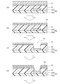
- the roughened surface of the copper foil 10 is bonded to the insulating resin substrate 12 having the lower layer circuit 12b on the base substrate 12a through the prepreg 14 (step (a)).
- via holes 16 are formed by laser drilling or drilling (step (c))
- Chemical copper plating 18 step (d)
- electrolytic copper plating 20 step (e)
- step (f) masking with a predetermined pattern by exposure and development using the dry film 22
- step (g) unnecessary copper foil and the like immediately below the opening of the dry film 22 are dissolved and removed by etching
- step (h) the dry film 22 is peeled off (step (h)) to obtain the wiring 24 formed in a predetermined pattern.
- the wiring 24 has a substantially trapezoidal cross section, and the bottom is wider than the top. If the distance of the extended portion (bottom portion) of the bottom with respect to the top end (referred to as the distance between the top and bottom) is large, the linearity of the circuit pattern is inferior. In this case, since the interval between the adjacent wirings 24 is locally narrowed, problems such as short circuits are likely to occur. In addition, the characteristic impedance does not match the predetermined resistance, resulting in poor high frequency characteristics.
- Patent Document 1 Japanese Patent Laid-Open No. 2008-285751
- the adhesive surface bonded to the insulating resin base material has a surface roughness (Rzjis) of 2.5 ⁇ m or less and a two-dimensional surface area of 6550 ⁇ m 2 .
- the surface area ratio (B) which is the value of the ratio [(A) / (6550)] of the three-dimensional surface area (A) ⁇ m 2 to the two-dimensional surface area when the region is measured by a laser method is 1.2 to 2.
- the surface-treated copper foil characterized by being 5 is disclosed.
- the roughening process and the antirust process are performed with respect to the deposition surface of an untreated electrolytic copper foil.
- Patent Document 2 International Publication No. 2015/033917 discloses a surface-treated copper foil obtained by performing a roughening treatment on the electrode surface side of an electrolytic copper foil, and the surface roughness Rz is 2.5-4.
- circuit linearity the linearity of the wiring pattern
- the inventors of the present invention have recently calculated the product of the arithmetic average height Sa ( ⁇ m) measured in accordance with ISO25178 and the peak vertex density Spd (pieces / mm 2 ) on the roughened surface of the roughened copper foil. And a specific surface profile of Sa ⁇ Spd of 250,000 ⁇ m / mm 2 or more and an arithmetic mean waviness Wa measured in accordance with JIS B0601-2001 is 0.030 to 0.060 ⁇ m.
- the inventors have obtained knowledge that both fine circuit formability (particularly circuit linearity) and adhesiveness with resin can be achieved.
- an object of the present invention is to provide a roughened copper foil that can achieve both fine circuit formability (particularly circuit linearity) and adhesion to a resin in processing a copper-clad laminate or manufacturing a printed wiring board. Is to provide.
- a roughened copper foil having a roughened surface on at least one side, wherein the roughened surface is an arithmetic average height Sa (measured in accordance with ISO25178). ⁇ m) and the peak density Spd (pieces / mm 2 ) of Sa ⁇ Spd is 250,000 ⁇ m / mm 2 or more, and the arithmetic average waviness Wa measured in accordance with JIS B0601-2001 is 0.00.
- a roughened copper foil having a thickness of 030 to 0.060 ⁇ m is provided.
- a copper-clad laminate including the roughened copper foil of the above aspect.
- a printed wiring board provided with the roughened copper foil of the above aspect is provided.
- Example 4 It is the SEM image which observed the wiring pattern obtained in Example 4 from the top.
- 6 is a cross-sectional SEM image of a wiring pattern obtained in Example 5.
- 10 is an SEM image obtained by observing the wiring pattern obtained in Example 5 from above. It is a figure for demonstrating the evaluation method of circuit linearity.
- arithmetic average height Sa is a parameter that represents an average of absolute values of height differences between points with respect to the average surface of the surface, measured in accordance with ISO25178. That is, it corresponds to a parameter obtained by extending the arithmetic average height Ra of the roughness curve to the surface.
- the arithmetic average height Sa can be calculated by measuring a surface profile of a predetermined measurement area (for example, a region of 22,500 ⁇ m 2 ) on the roughened surface with a commercially available laser microscope.
- the “mountain peak density Spd” is a parameter representing the number of peak apexes per unit area, measured in accordance with ISO25178. A large value suggests that the number of contact points with other objects is large.
- the peak vertex density Spd can be calculated by measuring a surface profile of a predetermined measurement area (for example, a region of 22,500 ⁇ m 2 ) on the roughened surface with a commercially available laser microscope.
- arithmetic mean wave Wa is an arithmetic average height at the reference length of a wave curve as a contour curve, measured according to JIS B0601-2001.
- the waviness curve is a contour curve obtained by sequentially applying a contour curve filter with cut-off values ⁇ f and ⁇ c to the cross-sectional curve, not the fine unevenness represented by the roughness curve. , Representing a larger scale irregularity (ie, undulation).
- the “electrode surface” of the electrolytic copper foil refers to the surface on the side in contact with the cathode when the electrolytic copper foil was produced.
- the “deposition surface” of the electrolytic copper foil refers to the surface on the side where the electrolytic copper is deposited during the production of the electrolytic copper foil, that is, the surface not in contact with the cathode.
- the copper foil of the present invention is a roughened copper foil.
- This roughened copper foil has a roughened surface on at least one side.
- the roughened surface has a Sa ⁇ Spd that is a product of the arithmetic average height Sa ( ⁇ m) measured according to ISO25178 and the peak density Spd (pieces / mm 2 ) of 250,000 ⁇ m / mm 2 or more.
- the arithmetic average waviness Wa measured in accordance with JIS B0601-2001 is 0.030 to 0.060 ⁇ m.
- the arithmetic average height Sa contributes to the biting of the roughened particles into the resin on the roughened surface
- the peak vertex density Spd contributes to securing the contact between the roughened particles and the resin on the roughened surface.
- Patent Document 1 it is common that the roughening treatment is performed on the deposition surface side of the electrolytic copper foil, but the low arithmetic average waviness Wa and the high Sa as described above in the present invention. It is considered that the coexistence of xSpd is difficult to realize on the deposition surface side of the electrolytic copper foil. This is because unevenness is generated in accordance with copper deposition on the deposition surface side of the electrolytic copper foil, and hence waviness must be increased.
- the surface of the rotating cathode is polished and smoothed in advance with a predetermined count buff, and an electrolytic copper foil is produced by electrolysis using the thus-rotated rotating cathode, ii)
- a roughening treatment under desired low roughening conditions on the electrode surface side (not on the deposition surface side) of the obtained untreated electrolytic copper foil, it is possible to obtain a unique characteristic with the low Wa and high Sa ⁇ Spd.
- the roughened surface can be desirably realized. Therefore, according to a preferred embodiment of the present invention, the roughened copper foil is an electrolytic copper foil, and the roughened surface is present on the electrode surface side of the electrolytic copper foil.
- Sa ⁇ Spd on the roughened surface is 250,000 ⁇ m / mm 2 or more, preferably 280000 to 500,000 ⁇ m / mm 2 .
- the adhesion to the resin can be further enhanced while ensuring the desired fine circuit formability (particularly circuit linearity).
- the arithmetic average waviness Wa on the roughened surface is 0.030 to 0.060 ⁇ m, preferably 0.030 to 0.050 ⁇ m, and more preferably 0.030 to 0.045 ⁇ m.
- Wa is within these ranges, fine circuit formability (particularly circuit linearity) can be further improved while ensuring high adhesion to the resin.
- the thickness of the roughened copper foil of the present invention is not particularly limited, but is preferably 0.1 to 35 ⁇ m, more preferably 0.5 to 18 ⁇ m.
- the roughening copper foil of this invention performed the roughening process or the fine roughening process of the copper foil surface not only what performed the roughening process on the surface of the normal copper foil but the copper foil with a carrier. It may be a thing.
- This preferred manufacturing method includes a step of preparing a copper foil having a surface with an arithmetic average waviness Wa of 0.030 to 0.060 ⁇ m, and a first roughening step of performing electrolytic deposition on the surface under predetermined conditions. A second roughening step in which electrolytic deposition is performed on the surface under predetermined conditions, and a third roughening process in which electrolytic deposition is performed on the surface under predetermined conditions to form a roughened surface. The process.
- the roughened copper foil according to the present invention is not limited to the method described below, and may be manufactured by any method.
- the surface of the rotating cathode is previously polished and smoothed with a predetermined count buff, and electrolysis using the thus polished cathode is performed.
- Electrolytic copper foil is preferable as the copper foil used for the production of the roughened copper foil. Further, the copper foil may be a non-roughened copper foil or a pre-roughened copper foil.
- the thickness of the copper foil is not particularly limited, but is preferably 0.1 to 35 ⁇ m, more preferably 0.5 to 18 ⁇ m.
- the copper foil is prepared by a wet film formation method such as an electroless copper plating method and an electrolytic copper plating method, a dry film formation method such as sputtering and chemical vapor deposition, or It may be formed by a combination thereof.
- the surface of the copper foil to be roughened preferably has a surface with an arithmetic average waviness Wa measured in accordance with JIS B0601-2001 of 0.030 to 0.060 ⁇ m, more preferably 0. 0.030 to 0.045 ⁇ m.
- the surface profile required for the roughened copper foil of the present invention in particular, the arithmetic average waviness of 0.030 to 0.060 ⁇ m can be easily imparted to the roughened surface.
- the electrode surface of the electrolytic copper foil has the arithmetic mean waviness Wa.
- the surface of the rotating cathode used for the production of the electrolytic copper foil is polished and smoothed beforehand with a buff, and the preferred count of such a buff is larger than # 1000, more preferably # 1200 to ##. 2500, more preferably # 1500 to # 2500.
- a buff By using such a buff, it becomes possible to impart the low Wa as described above to the electrode surface of the electrolytic copper foil.
- electrolytic deposition is performed at a temperature of 20 to 40 ° C. and 20 to 30 A / dm 2 in a copper sulfate solution containing a copper concentration of 8 to 12 g / L and a sulfuric acid concentration of 200 to 280 g / L.
- the electrolytic deposition is performed for 2 to 5 seconds.
- electrolytic deposition is performed at a temperature of 20 to 40 ° C. and 15 to 30 A / dm 2 in a copper sulfate solution containing a copper concentration of 8 to 12 g / L and a sulfuric acid concentration of 200 to 280 g / L.
- the electrolytic deposition is performed for 2 to 5 seconds. That is, the first roughening step and the second roughening step can be under the same conditions.
- electrolytic deposition is carried out at a temperature of 45 to 55 ° C.
- a roughened surface is preferably formed, and this electrolytic deposition is preferably performed for 5 to 25 seconds.
- a fine roughening treatment may be further performed on the roughening treatment surface formed in the third roughening step.
- the fine roughening treatment is performed at 20 to 40 ° C. in a copper sulfate solution having a copper concentration of 10 to 20 g / L, a sulfuric acid concentration of 30 to 130 g / L, a 9-phenylacridine concentration of 100 to 200 mg / L, and a chlorine concentration of 20 to 100 mg / L. It is preferable to carry out the electrolytic deposition of fine copper particles at a current density of 10 to 40 A / dm 2 at this temperature, and this electrolytic deposition is preferably carried out for 0.3 to 1.0 seconds.
- the copper foil after the roughening treatment may be subjected to a rust prevention treatment.
- the rust prevention treatment preferably includes a plating treatment using zinc.
- the plating treatment using zinc may be either a zinc plating treatment or a zinc alloy plating treatment, and the zinc alloy plating treatment is particularly preferably a zinc-nickel alloy treatment.
- the zinc-nickel alloy treatment may be a plating treatment containing at least Ni and Zn, and may further contain other elements such as Sn, Cr, and Co.
- the Ni / Zn adhesion ratio in the zinc-nickel alloy plating is preferably 1.2 to 10, more preferably 2 to 7, and still more preferably 2.7 to 4 in terms of mass ratio.
- the rust prevention treatment preferably further includes a chromate treatment, and this chromate treatment is more preferably performed on the surface of the plating containing zinc after the plating treatment using zinc.
- rust prevention property can further be improved.
- a particularly preferable antirust treatment is a combination of a zinc-nickel alloy plating treatment and a subsequent chromate treatment.
- the copper foil may be treated with a silane coupling agent to form a silane coupling agent layer.
- a silane coupling agent layer can be formed by appropriately diluting and applying a silane coupling agent and drying.
- silane coupling agents include epoxy-functional silane coupling agents such as 4-glycidylbutyltrimethoxysilane and 3-glycidoxypropyltrimethoxysilane, or 3-aminopropyltriethoxysilane, N-2 (amino Amino functions such as ethyl) 3-aminopropyltrimethoxysilane, N-3- (4- (3-aminopropoxy) butoxy) propyl-3-aminopropyltrimethoxysilane, N-phenyl-3-aminopropyltrimethoxysilane Silane coupling agents, or mercapto-functional silane coupling agents such as 3-mercaptopropyltrimethoxysilane, or olefin-functional silane coupling agents such as vinyltrimethoxysilane and vinylphenyltrimethoxysilane, or 3-methacryloxypropyl Trime Acrylic-functional silane coupling agent such as Kishishiran, or imid
- the roughened copper foil of the present invention is preferably used for the production of a copper-clad laminate for printed wiring boards. That is, according to the preferable aspect of this invention, the copper clad laminated board obtained using the said roughening process copper foil is provided.
- This copper-clad laminate includes the roughened copper foil of the present invention and a resin layer provided in close contact with the roughened surface of the roughened copper foil.
- the roughened copper foil may be provided on one side of the resin layer or on both sides.
- the resin layer comprises a resin, preferably an insulating resin.
- the resin layer is preferably a prepreg and / or a resin sheet.
- the prepreg is a general term for composite materials in which a base material such as a synthetic resin plate, a glass plate, a glass woven fabric, a glass nonwoven fabric, and paper is impregnated with a synthetic resin.
- a base material such as a synthetic resin plate, a glass plate, a glass woven fabric, a glass nonwoven fabric, and paper is impregnated with a synthetic resin.
- the insulating resin include an epoxy resin, a cyanate resin, a bismaleimide triazine resin (BT resin), a polyphenylene ether resin, and a phenol resin.
- the insulating resin that constitutes the resin sheet include insulating resins such as epoxy resins, polyimide resins, and polyester resins.
- the thickness of the resin layer is not particularly limited, but is preferably 1 to 1000 ⁇ m, more preferably 2 to 400 ⁇ m, and still more preferably 3 to 200 ⁇ m.
- the resin layer may be composed of a plurality of layers.
- a resin layer such as a prepreg and / or a resin sheet may be provided on the roughened copper foil via a primer resin layer applied to the surface of the copper foil in advance.
- the roughened copper foil of the present invention is preferably used for the production of a printed wiring board. That is, according to the preferable aspect of this invention, the printed wiring board obtained using the said roughening process copper foil is provided.
- the printed wiring board according to this aspect includes a layer configuration in which a resin layer and a copper layer are laminated in this order.
- the resin layer is as described above for the copper-clad laminate.
- a known layer structure can be adopted for the printed wiring board.
- a multilayer printed wiring board etc. are mentioned.
- Other specific examples include a flexible printed wiring board, a COF, a TAB tape, and the like that form a circuit by forming the roughened copper foil of the present invention on a resin film.
- a copper foil with resin (RCC) in which the above-described resin layer is applied to the roughened copper foil of the present invention is formed, and the resin layer is laminated on the above-described printed circuit board as an insulating adhesive layer.
- the build-up wiring board in which the circuit is formed by using the modified semi-additive (MSAP) method, the subtractive method, etc., with the roughened copper foil as a whole or a part of the wiring layer, and the roughened copper foil are removed.
- MSAP modified semi-additive
- Examples thereof include a build-up wiring board in which a circuit is formed by a semi-additive (SAP) method, and a direct build-up on wafer in which the lamination of a copper foil with resin and circuit formation are alternately repeated on a semiconductor integrated circuit.
- SAP semi-additive
- Roughening treatment was performed on the electrode surface side of the electrode surface and the precipitation surface included in the above-described electrolytic copper foil by a three-stage process shown below. That is, the 1st roughening process shown below, the 2nd roughening process, and the 3rd roughening process were performed in this order.
- the first roughening step is performed in Table 1A in a copper electrolytic solution for roughening treatment (copper concentration: 10.5 to 10.8 g / L, sulfuric acid concentration: 230 to 240 g / L) having the composition shown in Table 1A. It was carried out by electrolyzing under the indicated conditions and washing with water.
- the 2nd roughening process was performed by electrolyzing on the conditions shown by Table 1A in the copper electrolytic solution for roughening process of the same composition as a 1st roughening process, and washing with water.
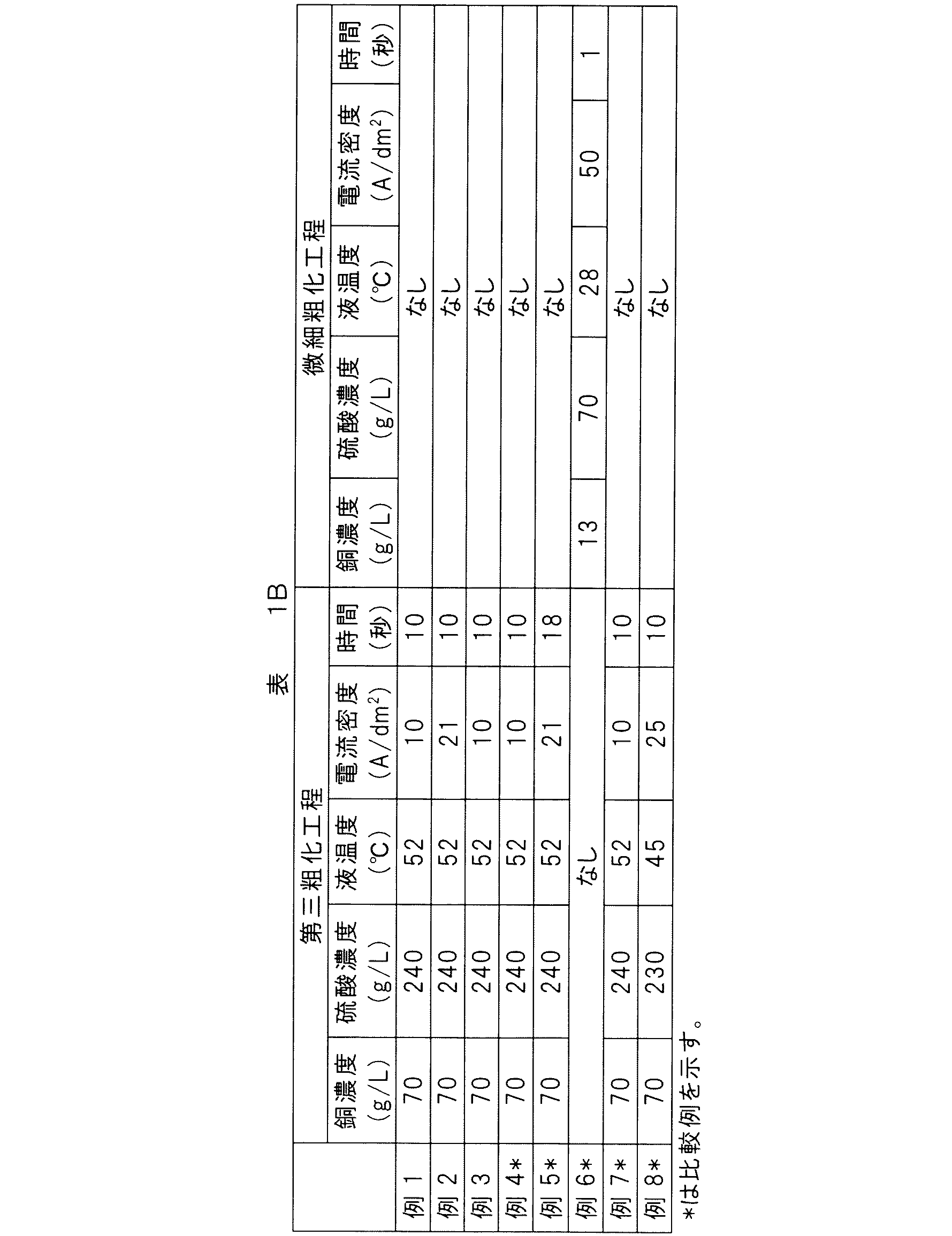
- the 3rd roughening process was performed by electrolyzing on the conditions shown by Table 1B in the copper electrolytic solution for a roughening process (copper concentration: 70 g / L, sulfuric acid concentration: 240 g / L), and washing with water.
- Rust prevention treatment comprising inorganic rust prevention treatment and chromate treatment was performed on both surfaces of the electrolytic copper foil after the roughening treatment.
- an inorganic rust prevention treatment using a pyrophosphate bath, potassium pyrophosphate concentration 80 g / L, zinc concentration 0.2 g / L, nickel concentration 2 g / L, liquid temperature 40 ° C., current density 0.5 A / dm 2 Zinc-nickel alloy rust prevention treatment was performed.
- a chromate treatment a chromate layer was further formed on the zinc-nickel alloy rust preventive treatment. This chromate treatment was performed at a chromic acid concentration of 1 g / L, pH 11, a solution temperature of 25 ° C., and a current density of 1 A / dm 2 .
- Silane coupling agent treatment The copper foil that has been subjected to the above rust prevention treatment is washed with water and then immediately treated with a silane coupling agent to adsorb the silane coupling agent onto the rust prevention treatment layer of the roughened surface. It was.
- this silane coupling agent treatment pure water is used as a solvent, a solution having a 3-aminopropyltrimethoxysilane concentration of 3 g / L is used, and this solution is sprayed onto the roughened surface by showering to perform an adsorption treatment. went. After adsorption of the silane coupling agent, water was finally evaporated by an electric heater to obtain a roughened copper foil having a thickness of 18 ⁇ m.
- Example 4 (Comparison) As shown in Tables 1A and 1B, a roughened copper foil was prepared in the same manner as in Example 1 except that the buff count used for polishing the rotating cathode was # 600.
- Example 5 (Comparison) i) Except that the electrolytic copper foil was subjected to a treatment such as a roughening treatment on the deposition surface side (that is, the side opposite to the electrode surface side), and ii) the roughening treatment was conducted according to the conditions shown in Tables 1A and 1B Prepared a roughened copper foil in the same manner as in Example 1.
- the roughening treatment surface of the roughening copper foil was basically affected by the count of the buff used for polishing the rotating cathode. Therefore, the buff count is not shown in Tables 1A and 2.
- Example 6 (Comparison) i) A roughening treatment or the like was performed on the deposition surface side (that is, the side opposite to the electrode surface side) of the electrolytic copper foil, and ii) the following 1 instead of the first, second and third roughening steps: A roughened copper foil was prepared in the same manner as in Example 1 except that the finer roughening process was performed.
- the roughening treatment surface of the roughening copper foil was basically affected by the count of the buff used for polishing the rotating cathode. Therefore, the buff count is not shown in Tables 1A and 2.
- the copper electrolytic solution for roughening treatment (copper concentration: 13 g / L, sulfuric acid concentration: 70 g / L, 9-phenylacridine concentration: In 140 mg / L, chlorine concentration: 35 mg / L), electrolysis was performed under the conditions shown in Table 1B, followed by washing with water to perform a fine roughening treatment.
- Example 7 (Comparison) As shown in Tables 1A and 1B, a roughened copper foil was prepared in the same manner as in Example 1 except that the buff count used for polishing the rotating cathode was # 3000.
- Example 8 (Comparison) i) The buff count used for polishing the rotating cathode was set to # 600, ii) the electrode surface side of the electrolytic copper foil was subjected to a treatment such as a roughening treatment, and iii) the first roughening step was performed using copper.
- a roughened copper foil was prepared in the same manner as in Example 1 except that the copper concentration was 70 g / L and the sulfuric acid concentration was 230 g / L, in accordance with the conditions shown in Table 1B. It was.
- ⁇ Arithmetic mean swell Wa> By means of surface roughness analysis using a laser microscope (manufactured by Keyence Corporation, VK-X100), the arithmetic average waviness Wa on the roughened surface of the roughened copper foil was measured in accordance with JIS B0601-2001. Specifically, the surface profile of a region (150 ⁇ m ⁇ 150 ⁇ m) having an area of 22,500 ⁇ m 2 on the roughened surface of the roughened copper foil was measured with the laser microscope at a magnification of 1000 times. Surface correction was performed on the surface profile of the obtained roughened surface, and then the surface was smoothed to a size of 5 ⁇ 5 by filtering, and waviness was measured by surface roughness analysis. The filter type was median.
- undulation Wa of the precipitation surface or electrode surface of the electrolytic copper foil before the roughening process in each example mentioned above was also performed in the same procedure as described above.
- ⁇ Sa ⁇ Spd> By surface property analysis using a laser microscope (manufactured by Keyence Corporation, VK-X100), the arithmetic average height Sa ( ⁇ m) and the peak density Spd (pieces / mm 2 ) on the roughened surface of the roughened copper foil ) In accordance with ISO25178. Specifically, the surface profile of a region (150 ⁇ m ⁇ 150 ⁇ m) having an area of 22500 ⁇ m 2 on the roughened surface of the roughened copper foil was measured at a magnification of 1000 times using the laser microscope. After surface inclination correction was performed on the surface profile of the obtained roughened surface, Sa and Spd were measured by surface property analysis. In this measurement, the cutoff wavelength by the S filter was 0.8 ⁇ m, and the cutoff wavelength by the L filter was 0.1 ⁇ m. Based on the values of Sa and Spd thus obtained, a value of Sa ⁇ Spd was calculated.
- ⁇ Peel strength> Two prepregs (EM355 (D), manufactured by ELITE MATERIAL CO., LTD) having a thickness of 50 ⁇ m were stacked to obtain a resin base material having a thickness of 100 ⁇ m. Laminated copper foil is laminated on this resin base material so that the roughened surface is in contact with the resin base material, and hot press molding is performed at a pressure of 4.0 MPa and a temperature of 185 ° C. for 60 minutes to obtain a copper-clad laminate. A plate sample was prepared. The copper-clad laminate sample was peeled in a 90 ° direction with respect to the resin substrate surface in accordance with JIS C 6481-1996, and the normal peel strength (kgf / cm) was measured.
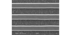
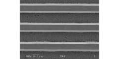
- FIG. 4B, 5B, and 6B the SEM image which observed the wiring pattern obtained in Examples 1, 4, and 5 from the top is shown to FIG. 4B, 5B, and 6B.
- FIG. 4A, 5A and 6A two substantially trapezoidal portions observed at the center are wiring patterns.
- FIG. 4B, 5B, and 6B three linear portions observed in the horizontal direction are wiring patterns.
- the cross section of the wiring pattern is substantially trapezoidal, and the width at the bottom is longer than the width at the top. It can be said that the smaller the variation in the distance (hereinafter referred to as the top-bottom distance) of the extended portion (bottom portion) of the bottom with respect to the top end of the wiring pattern, the higher the linearity of the circuit pattern.
- the wiring pattern shown in FIGS. 4A to 4B corresponding to Example 1 as an example is more than the wiring pattern shown in FIGS. 5A to 5B and 6A to 6B corresponding to Examples 4 and 5 as comparative examples.
- the linearity is high.
- the following measurement was performed.
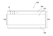
- the difference between one side of the top portion 102 and the bottom portion 104 of the circuit 100, that is, the above-described top-bottom distance D is set to 100 at intervals of 4 ⁇ m.
- the point was measured.
- the smaller one from the 26th top-bottom distance D 26 that is, the maximum value obtained by removing the measured values of the top 25% as noise
- Top 26 th counted from (75 th counted from the largest value) - bottom distance D 75 i.e. the minimum removal of 25% of the measured value lower as noise
Landscapes
- Chemical & Material Sciences (AREA)
- Engineering & Computer Science (AREA)
- Chemical Kinetics & Catalysis (AREA)
- Electrochemistry (AREA)
- Materials Engineering (AREA)
- Metallurgy (AREA)
- Organic Chemistry (AREA)
- Microelectronics & Electronic Packaging (AREA)
- Electroplating Methods And Accessories (AREA)
- Manufacturing Of Printed Wiring (AREA)
- Laminated Bodies (AREA)
- Parts Printed On Printed Circuit Boards (AREA)
- Manufacturing & Machinery (AREA)
Abstract
Description
本発明を特定するために用いられる用語ないしパラメータの定義を以下に示す。
本発明の銅箔は粗化処理銅箔である。この粗化処理銅箔は少なくとも一方の側に粗化処理面を有する。粗化処理面は、ISO25178に準拠して測定される算術平均高さSa(μm)と山の頂点密度Spd(個/mm2)の積であるSa×Spdが250000μm/mm2以上であり、かつ、JIS B0601-2001に準拠して測定される算術平均うねりWaが0.030~0.060μmである。このように、粗化処理銅箔の粗化処理面に、Sa×Spdが250000μm/mm2以上であり、かつ、算術平均うねりWaが0.030~0.060μmであるという特有の表面プロファイルを付与することにより、銅張積層板の加工ないしプリント配線板の製造において、微細回路形成性(特に回路直線性)と、樹脂との密着性とを両立することが可能となる。前述したとおり、回路直線性と樹脂との密着性は、銅箔の表面プロファイルに対してトレードオフの関係にあるため、本来的に両立が難しいとの問題があったが、本発明の粗化処理銅箔によれば、良好な回路直線性と樹脂との高い密着性を予想外にも両立することができる。
本発明による粗化処理銅箔の好ましい製造方法の一例を説明する。この好ましい製造方法は、算術平均うねりWaが0.030~0.060μmの表面を有する銅箔を用意する工程と、上記表面に対して所定の条件にて電解析出を行う第一粗化工程と、上記表面に対して所定の条件にて電解析出を行う第二粗化工程と、上記表面に対して所定の条件にて電解析出を行って粗化処理面を形成する第三粗化工程とを含んでなる。もっとも、本発明による粗化処理銅箔は以下に説明する方法に限らず、あらゆる方法によって製造されたものであってよい。特に、前述したように、本発明の粗化処理銅箔においては、(i)回転陰極の表面を予め所定の番手のバフで研磨して平滑化しておき、こうして研磨した陰極を用いた電解により電解銅箔を製造し、さらに(ii)得られた未処理の電解銅箔の(析出面側ではなく)電極面側に所望の低粗化条件で粗化処理を行うことにより、上記低いWa及び高いSa×Spdを備えた特有の粗化処理面を望ましく実現することができる。具体的には以下のとおりである。
粗化処理銅箔の製造に使用する銅箔としては電解銅箔が好ましい。また、銅箔は、無粗化の銅箔であってもよいし、予備的粗化を施したものであってもよい。銅箔の厚さは特に限定されないが、0.1~35μmが好ましく、より好ましくは0.5~18μmである。銅箔がキャリア付銅箔の形態で準備される場合には、銅箔は、無電解銅めっき法及び電解銅めっき法等の湿式成膜法、スパッタリング及び化学蒸着等の乾式成膜法、又はそれらの組合せにより形成したものであってよい。
こうして上記低いWaが付与された電解銅箔の表面(すなわち電極面)に対して、第一粗化工程、第二粗化工程、第三粗化工程の3段階の粗化工程を施すのが好ましい。第一粗化工程では、銅濃度8~12g/L及び硫酸濃度200~280g/Lを含む硫酸銅溶液中、20~40℃の温度で、20~30A/dm2にて電解析出を行うのが好ましく、この電解析出は2~5秒間行われるのが好ましい。第二粗化工程では、銅濃度8~12g/L及び硫酸濃度200~280g/Lを含む硫酸銅溶液中、20~40℃の温度で、15~30A/dm2にて電解析出を行うのが好ましく、この電解析出は2~5秒間行われるのが好ましい。すなわち、第一粗化工程と第二粗化工程は同じ条件であることができる。第三粗化工程では、銅濃度65~80g/L及び硫酸濃度200~280g/Lを含む硫酸銅溶液中、45~55℃の温度で、10~30A/dm2にて電解析出を行って粗化処理面を形成するのが好ましく、この電解析出は5~25秒間行われるのが好ましい。
所望により、第三粗化工程で形成された粗化処理面に対して微細粗化処理がさらに行われてもよい。微細粗化処理は、銅濃度10~20g/L、硫酸濃度30~130g/L、9-フェニルアクリジン濃度100~200mg/L、塩素濃度20~100mg/Lの硫酸銅溶液中、20~40℃の温度で、電流密度10~40A/dm2で微細銅粒子を電解析出させることにより行われるのが好ましく、この電解析出は0.3~1.0秒間行われるのが好ましい。
所望により、粗化処理後の銅箔に防錆処理を施してもよい。防錆処理は、亜鉛を用いためっき処理を含むのが好ましい。亜鉛を用いためっき処理は、亜鉛めっき処理及び亜鉛合金めっき処理のいずれであってもよく、亜鉛合金めっき処理は亜鉛-ニッケル合金処理が特に好ましい。亜鉛-ニッケル合金処理は少なくともNi及びZnを含むめっき処理であればよく、Sn、Cr、Co等の他の元素をさらに含んでいてもよい。亜鉛-ニッケル合金めっきにおけるNi/Zn付着比率は、質量比で、1.2~10が好ましく、より好ましくは2~7、さらに好ましくは2.7~4である。また、防錆処理はクロメート処理をさらに含むのが好ましく、このクロメート処理は亜鉛を用いためっき処理の後に、亜鉛を含むめっきの表面に行われるのがより好ましい。こうすることで防錆性をさらに向上させることができる。特に好ましい防錆処理は、亜鉛-ニッケル合金めっき処理とその後のクロメート処理との組合せである。
所望により、銅箔にシランカップリング剤処理を施し、シランカップリング剤層を形成してもよい。これにより耐湿性、耐薬品性及び接着剤等との密着性等を向上することができる。シランカップリング剤層は、シランカップリング剤を適宜希釈して塗布し、乾燥させることにより形成することができる。シランカップリング剤の例としては、4-グリシジルブチルトリメトキシシラン、3-グリシドキシプロピルトリメトキシシラン等のエポキシ官能性シランカップリング剤、又は3-アミノプロピルトリエトキシシラン、N-2(アミノエチル)3-アミノプロピルトリメトキシシラン、N-3-(4-(3-アミノプロポキシ)ブトキシ)プロピル-3-アミノプロピルトリメトキシシラン、N-フェニル-3-アミノプロピルトリメトキシシラン等のアミノ官能性シランカップリング剤、又は3-メルカプトプロピルトリメトキシシラン等のメルカプト官能性シランカップリング剤又はビニルトリメトキシシラン、ビニルフェニルトリメトキシシラン等のオレフィン官能性シランカップリング剤、又は3-メタクリロキシプロピルトリメトキシシラン等のアクリル官能性シランカップリング剤、又はイミダゾールシラン等のイミダゾール官能性シランカップリング剤、又はトリアジンシラン等のトリアジン官能性シランカップリング剤等が挙げられる。
本発明の粗化処理銅箔はプリント配線板用銅張積層板の作製に用いられるのが好ましい。すなわち、本発明の好ましい態様によれば、上記粗化処理銅箔を用いて得られた銅張積層板が提供される。この銅張積層板は、本発明の粗化処理銅箔と、この粗化処理銅箔の粗化処理面に密着して設けられる樹脂層とを備えてなる。粗化処理銅箔は樹脂層の片面に設けられてもよいし、両面に設けられてもよい。樹脂層は、樹脂、好ましくは絶縁性樹脂を含んでなる。樹脂層はプリプレグ及び/又は樹脂シートであるのが好ましい。プリプレグとは、合成樹脂板、ガラス板、ガラス織布、ガラス不織布、紙等の基材に合成樹脂を含浸させた複合材料の総称である。絶縁性樹脂の好ましい例としては、エポキシ樹脂、シアネート樹脂、ビスマレイミドトリアジン樹脂(BT樹脂)、ポリフェニレンエーテル樹脂、フェノール樹脂等が挙げられる。また、樹脂シートを構成する絶縁性樹脂の例としては、エポキシ樹脂、ポリイミド樹脂、ポリエステル樹脂等の絶縁樹脂が挙げられる。また、樹脂層には絶縁性を向上する等の観点からシリカ、アルミナ等の各種無機粒子からなるフィラー粒子等が含有されていてもよい。樹脂層の厚さは特に限定されないが、1~1000μmが好ましく、より好ましくは2~400μmであり、さらに好ましくは3~200μmである。樹脂層は複数の層で構成されていてよい。プリプレグ及び/又は樹脂シート等の樹脂層は予め銅箔表面に塗布されるプライマー樹脂層を介して粗化処理銅箔に設けられていてもよい。
本発明の粗化処理銅箔はプリント配線板の作製に用いられるのが好ましい。すなわち、本発明の好ましい態様によれば、上記粗化処理銅箔を用いて得られたプリント配線板が提供される。本態様によるプリント配線板は、樹脂層と、銅層とがこの順に積層された層構成を含んでなる。また、樹脂層については銅張積層板に関して上述したとおりである。いずれにしても、プリント配線板は公知の層構成が採用可能である。プリント配線板に関する具体例としては、プリプレグの片面又は両面に本発明の粗化処理銅箔を接着させ硬化した積層体とした上で回路形成した片面又は両面プリント配線板や、これらを多層化した多層プリント配線板等が挙げられる。また、他の具体例としては、樹脂フィルム上に本発明の粗化処理銅箔を形成して回路を形成するフレキシブルプリント配線板、COF、TABテープ等も挙げられる。さらに他の具体例としては、本発明の粗化処理銅箔に上述の樹脂層を塗布した樹脂付銅箔(RCC)を形成し、樹脂層を絶縁接着材層として上述のプリント基板に積層した後、粗化処理銅箔を配線層の全部又は一部としてモディファイド・セミアディティブ(MSAP)法、サブトラクティブ法等の手法で回路を形成したビルドアップ配線板や、粗化処理銅箔を除去してセミアディティブ(SAP)法で回路を形成したビルドアップ配線板、半導体集積回路上へ樹脂付銅箔の積層と回路形成を交互に繰りかえすダイレクト・ビルドアップ・オン・ウェハー等が挙げられる。
本発明の粗化処理銅箔の作製を以下のようにして行った。
銅電解液として以下に示される組成の硫酸酸性硫酸銅溶液を用い、陰極にチタン製の回転電極を用い、陽極にはDSA(寸法安定性陽極)を用いて、溶液温度45℃、電流密度55A/dm2で電解し、厚さ12μmの電解銅箔を得た。このとき、回転陰極として、表面を#1200(例1)、#2000(例2)又は#1500(例3)のホイールバフで研磨して表面粗さを調整した電極を用いた。この電解銅箔の電極面の算術平均うねりWaを後述する手法にて測定したところ、表2に示される値が得られた。
<硫酸酸性硫酸銅溶液の組成>
‐ 銅濃度:80g/L
‐ 硫酸濃度:260g/L
‐ ビス(3-スルホプロピル)ジスルフィド濃度:30mg/L
‐ ジアリルジメチルアンモニウムクロライド重合体濃度:50mg/L
‐ 塩素濃度:40mg/L
上述の電解銅箔が備える電極面及び析出面の内、電極面側に対して、以下に示される3段階のプロセスで粗化処理を行った。すなわち、以下に示される第一粗化工程、第二粗化工程及び第三粗化工程をこの順に行った。
‐ 第一粗化工程は、表1Aに示される組成の粗化処理用銅電解溶液(銅濃度:10.5~10.8g/L、硫酸濃度:230~240g/L)中、表1Aに示される条件にて電解し、水洗することにより行った。
‐ 第二粗化工程は、第一粗化工程と同じ組成の粗化処理用銅電解溶液中、表1Aに示される条件にて電解し、水洗することにより行った。
‐ 第三粗化工程は、粗化処理用銅電解溶液(銅濃度:70g/L、硫酸濃度:240g/L)中、表1Bに示される条件にて電解し、水洗することにより行った。
粗化処理後の電解銅箔の両面に、無機防錆処理及びクロメート処理からなる防錆処理を行った。まず、無機防錆処理として、ピロリン酸浴を用い、ピロリン酸カリウム濃度80g/L、亜鉛濃度0.2g/L、ニッケル濃度2g/L、液温40℃、電流密度0.5A/dm2で亜鉛-ニッケル合金防錆処理を行った。次いで、クロメート処理として、亜鉛-ニッケル合金防錆処理の上に、更にクロメート層を形成した。このクロメート処理は、クロム酸濃度が1g/L、pH11、溶液温度25℃、電流密度1A/dm2で行った。
上記防錆処理が施された銅箔を水洗し、その後直ちにシランカップリング剤処理を行い、粗化処理面の防錆処理層上にシランカップリング剤を吸着させた。このシランカップリング剤処理は、純水を溶媒とし、3-アミノプロピルトリメトキシシラン濃度が3g/Lの溶液を用い、この溶液をシャワーリングにて粗化処理面に吹き付けて吸着処理することにより行った。シランカップリング剤の吸着後、最終的に電熱器により水分を蒸発させ、厚さ18μmの粗化処理銅箔を得た。
表1A及び1Bに示されるとおり、回転陰極の研磨に用いたバフの番手を#600としたこと以外は、例1と同様にして、粗化処理銅箔の作製を行った。
i)電解銅箔の析出面側(すなわち電極面側と反対側)に粗化処理等の処理を行ったこと、及びii)粗化処理を表1A及び1Bに示される条件に従って行ったこと以外は例1と同様にして、粗化処理銅箔の作製を行った。なお、本例においては電解銅箔の析出面側に粗化処理等を行ったため、粗化処理銅箔の粗化処理面は回転陰極の研磨に用いたバフの番手の影響を基本的に受けないため、表1A及び2においてバフの番手の記載を省略した。
i)電解銅箔の析出面側(すなわち電極面側と反対側)に粗化処理等の処理を行ったこと、及びii)第一、第二及び第三粗化工程の代わりに以下の1段階の微細粗化処理を行ったこと以外は例1と同様にして、粗化処理銅箔の作製を行った。なお、本例においては電解銅箔の析出面側に粗化処理等を行ったため、粗化処理銅箔の粗化処理面は回転陰極の研磨に用いたバフの番手の影響を基本的に受けないため、表1A及び2においてバフの番手の記載を省略した。
上述の電解銅箔が備える電極面及び析出面の内、析出面側に対して、粗化処理用銅電解溶液(銅濃度:13g/L、硫酸濃度:70g/L、9-フェニルアクリジン濃度:140mg/L、塩素濃度:35mg/L)中、表1Bに示される条件にて電解し、水洗することにより、微細粗化処理を行った。
表1A及び1Bに示されるとおり、回転陰極の研磨に用いたバフの番手を#3000としたこと以外は、例1と同様にして、粗化処理銅箔の作製を行った。
i)回転陰極の研磨に用いたバフの番手を#600としたこと、ii)電解銅箔の電極面側に粗化処理等の処理を行ったこと、iii)第一粗化工程を、銅濃度:8g/L、硫酸濃度:230g/L、及びニカワ濃度:2mg/Lの粗化処理用電解溶液中、表1Aに示される条件に従って行ったこと、及びiv)第三粗化工程を、銅濃度:70g/L及び硫酸濃度:230g/Lの粗化処理用電解溶液中、表1Bに示される条件に従って行ったこと以外は例1と同様にして、粗化処理銅箔の作製を行った。

例1~7において作製された粗化処理銅箔について、以下に示される各種評価を行った。
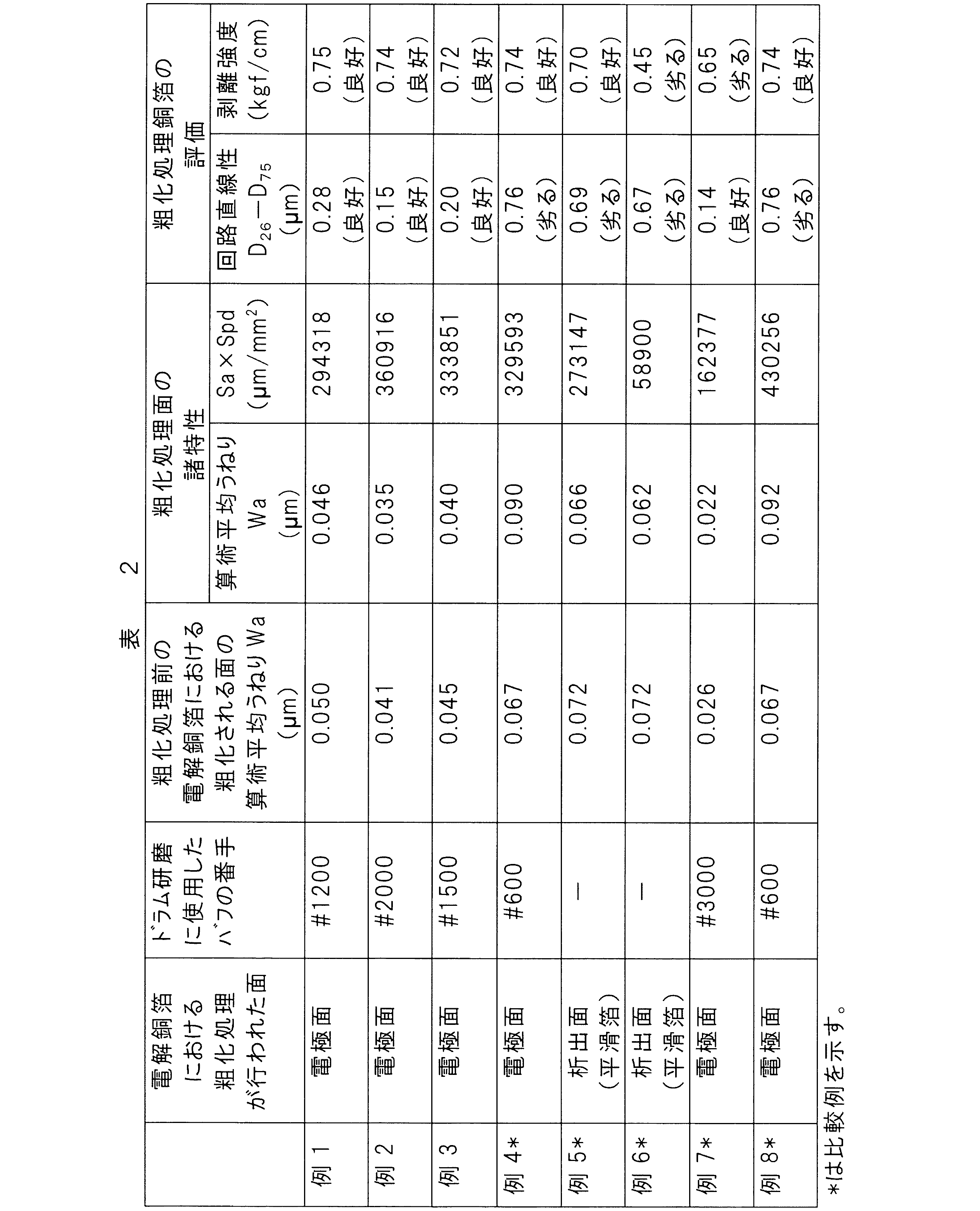
レーザー顕微鏡(株式会社キーエンス製、VK-X100)を用いた表面粗さ解析により、粗化処理銅箔の粗化処理面における算術平均うねりWaの測定をJIS B0601-2001に準拠して行った。具体的には、粗化処理銅箔の粗化処理面における面積22500μm2の領域(150μm×150μm)の表面プロファイルを上記レーザー顕微鏡にて倍率1000倍で測定した。得られた粗化処理面の表面プロファイルに対して面傾き補正を行った後、フィルター処理にてサイズ5×5に平滑化し、表面粗さ解析によりうねり測定を実施した。フィルタータイプはメディアンとした。また、各輪郭曲線フィルターのカットオフ値は、λs=0.25μm、λc=0.08mm、λf=80μmとした。なお、前述した各例における粗化処理前の電解銅箔の析出面又は電極面の算術平均うねりWaの測定も上記同様の手順にて行われた。
レーザー顕微鏡(株式会社キーエンス製、VK-X100)を用いた表面性状解析により、粗化処理銅箔の粗化処理面における算術平均高さSa(μm)と山の頂点密度Spd(個/mm2)のISO25178に準拠して行った。具体的には、粗化処理銅箔の粗化処理面における面積22500μm2の領域(150μm×150μm)の表面プロファイルを、上記レーザー顕微鏡を用いて倍率1000倍で測定した。得られた粗化処理面の表面プロファイルに対して面傾き補正を行った後、表面性状解析によりSa及びSpdの測定を実施した。この測定は、Sフィルターによるカットオフ波長を0.8μmとし、Lフィルターによるカットオフ波長を0.1μmとして行った。こうして得られたSa及びSpdの値に基づいてSa×Spdの値を算出した。
厚さ50μmのプリプレグ(EM355(D)、ELITE MATERIAL CO., LTD製)2枚を重ねて厚さ100μmの樹脂基材を得た。この樹脂基材に粗化処理銅箔をその粗化処理面が樹脂基材と当接するように積層し、圧力4.0MPa及び温度185℃で60分間の熱間プレス成形を行って銅張積層板サンプルを作製した。この銅張積層板サンプルに対して、JIS C 6481-1996に準拠して、樹脂基材面に対して90°方向に剥離して常態剥離強度(kgf/cm)を測定した。
回路直線性の評価を次のようにして行った。まず、上述の銅張積層板の表面に回路高さが20μmになるまで電気めっきを行った。こうして形成された電気めっき層の表面にドライフィルムを貼り付け、露光及び現像を行い、エッチングレジストを形成した。塩化銅エッチング液で処理することにより、レジスト間から銅を溶解除去し、回路高さ20μm、ライン/スペース(L/S)=30μm/30μmの直線状配線パターンを形成した。こうして得られた直線状配線パターンをSEMで観察した。例1、4及び5で得られた配線パターンの断面SEM画像をそれぞれ図4A、5A及び6Aに示す。また、例1、4及び5で得られた配線パターンを上から観察したSEM画像を図4B、5B及び6Bに示す。図4A、5A及び6Aにおいて中央に観察される2つの略台形状の部分が配線パターンである。また、図4B、5B及び6Bにおいて横方向に3本観察される直線部分が配線パターンである。これらの図から分かるように、配線パターンの断面は略台形状であり、頂部における幅よりも底部における幅は長くなる。そして、配線パターンの頂部の端を基準とした底部の延出部分(裾野部分)の距離(以下、トップ-ボトム間距離という)のばらつきが少ない程、回路パターンの直線性が高いといえる。この点、比較例である例4及び5に相当する図5A~5B及び6A~6Bに示される配線パターンよりも、実施例である例1に相当する図4A~4Bに示される配線パターンの方が、直線性が高いことが分かる。
例1~7において得られた評価結果は表2に示されるとおりであった。表2に示されるように、本発明の条件を満たす例1~3で作製した粗化処理銅箔は、微細回路形成性(特に回路直線性)と、樹脂との密着性との両方に優れるものであった。
Claims (6)
- 少なくとも一方の側に粗化処理面を有する粗化処理銅箔であって、前記粗化処理面は、ISO25178に準拠して測定される算術平均高さSa(μm)と山の頂点密度Spd(個/mm2)の積であるSa×Spdが250000μm/mm2以上であり、かつ、JIS B0601-2001に準拠して測定される算術平均うねりWaが0.030~0.060μmである、粗化処理銅箔。
- 前記Sa×Spdが280000~500000μm/mm2である、請求項1に記載の粗化処理銅箔。
- 前記算術平均うねりWaが0.033~0.050μmである、請求項1又は2に記載の粗化処理銅箔。
- 前記粗化処理銅箔が電解銅箔であり、前記粗化処理面が電解銅箔の電極面側に存在する、請求項1~3のいずれか一項に記載の粗化処理銅箔。
- 請求項1~4のいずれか一項に記載の粗化処理銅箔を備えた、銅張積層板。
- 請求項1~4のいずれか一項に記載の粗化処理銅箔を備えた、プリント配線板。
Priority Applications (4)
| Application Number | Priority Date | Filing Date | Title |
|---|---|---|---|
| KR1020177034238A KR101895745B1 (ko) | 2015-07-03 | 2016-06-16 | 조면화 처리 동박, 동장 적층판 및 프린트 배선판 |
| CN201680031199.1A CN107614760B (zh) | 2015-07-03 | 2016-06-16 | 粗糙化处理铜箔、覆铜层叠板和印刷电路板 |
| JP2017526725A JP6193534B2 (ja) | 2015-07-03 | 2016-06-16 | 粗化処理銅箔、銅張積層板及びプリント配線板 |
| PH12017502362A PH12017502362B1 (en) | 2015-07-03 | 2017-12-19 | Roughened copper foil, copper-clad laminate and printed wiring board |
Applications Claiming Priority (2)
| Application Number | Priority Date | Filing Date | Title |
|---|---|---|---|
| JP2015-134707 | 2015-07-03 | ||
| JP2015134707 | 2015-07-03 |
Publications (1)
| Publication Number | Publication Date |
|---|---|
| WO2017006739A1 true WO2017006739A1 (ja) | 2017-01-12 |
Family
ID=57686211
Family Applications (1)
| Application Number | Title | Priority Date | Filing Date |
|---|---|---|---|
| PCT/JP2016/067972 Ceased WO2017006739A1 (ja) | 2015-07-03 | 2016-06-16 | 粗化処理銅箔、銅張積層板及びプリント配線板 |
Country Status (7)
| Country | Link |
|---|---|
| JP (1) | JP6193534B2 (ja) |
| KR (1) | KR101895745B1 (ja) |
| CN (1) | CN107614760B (ja) |
| MY (1) | MY177676A (ja) |
| PH (1) | PH12017502362B1 (ja) |
| TW (1) | TWI630289B (ja) |
| WO (1) | WO2017006739A1 (ja) |
Cited By (22)
| Publication number | Priority date | Publication date | Assignee | Title |
|---|---|---|---|---|
| WO2017179416A1 (ja) * | 2016-04-14 | 2017-10-19 | 三井金属鉱業株式会社 | 表面処理銅箔、キャリア付銅箔、並びにそれらを用いた銅張積層板及びプリント配線板の製造方法 |
| WO2018211951A1 (ja) * | 2017-05-19 | 2018-11-22 | 三井金属鉱業株式会社 | 粗化処理銅箔、キャリア付銅箔、銅張積層板及びプリント配線板 |
| WO2019208525A1 (ja) * | 2018-04-27 | 2019-10-31 | Jx金属株式会社 | 表面処理銅箔、銅張積層板及びプリント配線板 |
| JP2020050954A (ja) * | 2018-09-26 | 2020-04-02 | 金居開發股▲分▼有限公司 | 微小粗面化電解銅箔及び銅箔基板 |
| JP2020063492A (ja) * | 2018-10-18 | 2020-04-23 | Jx金属株式会社 | 導電性材料、成型品及び電子部品 |
| JP2020076151A (ja) * | 2018-11-05 | 2020-05-21 | 金居開發股▲分▼有限公司 | マイクロラフ処理された電解銅箔及びこれを用いた銅張基板 |
| WO2020105289A1 (ja) * | 2018-11-19 | 2020-05-28 | 三井金属鉱業株式会社 | 表面処理銅箔、キャリア付銅箔、銅張積層板及びプリント配線板 |
| CN111433404A (zh) * | 2017-12-13 | 2020-07-17 | 株式会社可乐丽 | 经印刷的起毛片及印刷用起毛片 |
| JP2020128589A (ja) * | 2019-02-01 | 2020-08-27 | 長春石油化學股▲分▼有限公司 | 表面処理銅箔 |
| CN112118672A (zh) * | 2019-06-19 | 2020-12-22 | 金居开发股份有限公司 | 具有长岛状微结构的进阶反转电解铜箔及应用其的铜箔基板 |
| JP2021001398A (ja) * | 2019-06-19 | 2021-01-07 | 金居開發股▲分▼有限公司 | ミクロ粗面化した電着銅箔及び銅張積層板 |
| JP2021021137A (ja) * | 2019-06-19 | 2021-02-18 | 金居開發股▲分▼有限公司 | 長尺島状の微細構造を有するアドバンスト電解銅箔及びそれを適用した銅張積層板 |
| JPWO2020031721A1 (ja) * | 2018-08-10 | 2021-04-30 | 三井金属鉱業株式会社 | 粗化処理銅箔、キャリア付銅箔、銅張積層板及びプリント配線板 |
| US11162151B2 (en) | 2016-11-09 | 2021-11-02 | Kubota Corporation | Tube body that is to be used in high-temperature atmosphere and method for forming metal oxide layer on inner surface of tube body |
| JPWO2023281778A1 (ja) * | 2021-07-09 | 2023-01-12 | ||
| JPWO2023281776A1 (ja) * | 2021-07-09 | 2023-01-12 | ||
| JPWO2023281777A1 (ja) * | 2021-07-09 | 2023-01-12 | ||
| JPWO2023281775A1 (ja) * | 2021-07-09 | 2023-01-12 | ||
| JPWO2023281774A1 (ja) * | 2021-07-09 | 2023-01-12 | ||
| WO2023119513A1 (ja) * | 2021-12-22 | 2023-06-29 | 三井金属鉱業株式会社 | 銅箔の表面パラメータの測定方法、銅箔の選別方法、及び表面処理銅箔の製造方法 |
| CN117480282A (zh) * | 2021-06-03 | 2024-01-30 | 三井金属矿业株式会社 | 粗糙化处理铜箔、覆铜层叠板和印刷电路板 |
| TWI895668B (zh) * | 2022-12-20 | 2025-09-01 | 日商三井金屬鑛業股份有限公司 | 銅箔的表面參數的測定方法、及銅箔的選別方法 |
Families Citing this family (13)
| Publication number | Priority date | Publication date | Assignee | Title |
|---|---|---|---|---|
| JP6400875B1 (ja) * | 2018-02-14 | 2018-10-03 | 住友化学株式会社 | 積層体 |
| TWI668333B (zh) * | 2018-09-17 | 2019-08-11 | 金居開發股份有限公司 | 微粗糙電解銅箔及銅箔基板 |
| CN111194134B (zh) * | 2018-11-15 | 2021-11-02 | 金居开发股份有限公司 | 经微细粗糙化处理的电解铜箔以及使用其的覆铜基板 |
| CN113545181B (zh) * | 2019-03-19 | 2024-10-11 | 拓自达电线株式会社 | 屏蔽印制线路板、屏蔽印制线路板的制造方法以及连接构件 |
| JP7392996B2 (ja) | 2019-06-19 | 2023-12-06 | 金居開發股▲分▼有限公司 | アドバンスド電解銅箔及びそれを適用した銅張積層板 |
| JP7421208B2 (ja) * | 2019-12-24 | 2024-01-24 | 日本電解株式会社 | 表面処理銅箔及びその製造方法 |
| JP7259093B2 (ja) * | 2020-02-04 | 2023-04-17 | 三井金属鉱業株式会社 | 粗化処理銅箔、キャリア付銅箔、銅張積層板及びプリント配線板 |
| KR102832557B1 (ko) * | 2020-02-04 | 2025-07-11 | 미쓰이금속광업주식회사 | 조화 처리 동박, 캐리어를 구비하는 동박, 동장 적층판 및 프린트 배선판 |
| US10991948B1 (en) * | 2020-03-20 | 2021-04-27 | Chang Chun Petrochemical Co., Ltd. | Surface-treated copper foil for lithium-ion secondary batteries |
| JP7374298B2 (ja) * | 2020-03-23 | 2023-11-06 | 三井金属鉱業株式会社 | 粗化処理銅箔、銅張積層板及びプリント配線板 |
| KR102454686B1 (ko) | 2020-12-30 | 2022-10-13 | 에스케이씨 주식회사 | 표면 처리 동박 및 이를 포함하는 회로 기판 |
| KR102506594B1 (ko) | 2021-04-09 | 2023-03-03 | 에스케이씨 주식회사 | 표면 처리 동박 및 이를 포함하는 회로 기판 |
| CN117321254A (zh) * | 2021-05-20 | 2023-12-29 | 三井金属矿业株式会社 | 粗糙化处理铜箔、带载体的铜箔、覆铜层叠板及印刷电路板 |
Citations (4)
| Publication number | Priority date | Publication date | Assignee | Title |
|---|---|---|---|---|
| JP2004263296A (ja) * | 2003-02-12 | 2004-09-24 | Furukawa Techno Research Kk | ファインパターンプリント配線用銅箔とその製造方法 |
| JP2013019056A (ja) * | 2006-03-10 | 2013-01-31 | Mitsui Mining & Smelting Co Ltd | 表面処理電解銅箔及びその表面処理銅箔を用いて得られる銅張積層板 |
| US20130220679A1 (en) * | 2010-10-06 | 2013-08-29 | Furukawa Electric Co., Ltd. | Copper foil and manufacturing method therefor, copper foil with carrier and manufacturing method therefor, printed circuit board, and multilayer printed circuit board |
| JP2014201777A (ja) * | 2013-04-02 | 2014-10-27 | Jx日鉱日石金属株式会社 | キャリア付き銅箔 |
Family Cites Families (7)
| Publication number | Priority date | Publication date | Assignee | Title |
|---|---|---|---|---|
| TW200500199A (en) * | 2003-02-12 | 2005-01-01 | Furukawa Circuit Foil | Copper foil for fine patterned printed circuits and method of production of same |
| CN100591809C (zh) * | 2007-01-25 | 2010-02-24 | 湖北中科铜箔科技有限公司 | 电解铜箔表面低粗化处理方法 |
| JP5129642B2 (ja) | 2007-04-19 | 2013-01-30 | 三井金属鉱業株式会社 | 表面処理銅箔及びその表面処理銅箔を用いて得られる銅張積層板並びにその銅張積層板を用いて得られるプリント配線板 |
| TWI434965B (zh) * | 2008-05-28 | 2014-04-21 | Mitsui Mining & Smelting Co | A roughening method for copper foil, and a copper foil for a printed wiring board which is obtained by the roughening method |
| EP2644754B1 (en) * | 2010-11-22 | 2016-05-11 | Mitsui Mining & Smelting Co., Ltd. | Surface treated copper foil |
| KR20140124402A (ko) * | 2012-11-26 | 2014-10-24 | 제이엑스 닛코 닛세키 킨조쿠 가부시키가이샤 | 표면 처리 전해 동박, 적층판, 및 프린트 배선판 |
| TWI515342B (zh) | 2013-09-05 | 2016-01-01 | 三井金屬鑛業股份有限公司 | 表面處理銅箔、使用該表面處理銅箔所得之貼銅積層板以及印刷配線板 |
-
2016
- 2016-06-16 KR KR1020177034238A patent/KR101895745B1/ko active Active
- 2016-06-16 WO PCT/JP2016/067972 patent/WO2017006739A1/ja not_active Ceased
- 2016-06-16 CN CN201680031199.1A patent/CN107614760B/zh active Active
- 2016-06-16 JP JP2017526725A patent/JP6193534B2/ja active Active
- 2016-06-16 MY MYPI2017705033A patent/MY177676A/en unknown
- 2016-06-27 TW TW105120194A patent/TWI630289B/zh active
-
2017
- 2017-12-19 PH PH12017502362A patent/PH12017502362B1/en unknown
Patent Citations (4)
| Publication number | Priority date | Publication date | Assignee | Title |
|---|---|---|---|---|
| JP2004263296A (ja) * | 2003-02-12 | 2004-09-24 | Furukawa Techno Research Kk | ファインパターンプリント配線用銅箔とその製造方法 |
| JP2013019056A (ja) * | 2006-03-10 | 2013-01-31 | Mitsui Mining & Smelting Co Ltd | 表面処理電解銅箔及びその表面処理銅箔を用いて得られる銅張積層板 |
| US20130220679A1 (en) * | 2010-10-06 | 2013-08-29 | Furukawa Electric Co., Ltd. | Copper foil and manufacturing method therefor, copper foil with carrier and manufacturing method therefor, printed circuit board, and multilayer printed circuit board |
| JP2014201777A (ja) * | 2013-04-02 | 2014-10-27 | Jx日鉱日石金属株式会社 | キャリア付き銅箔 |
Cited By (68)
| Publication number | Priority date | Publication date | Assignee | Title |
|---|---|---|---|---|
| JPWO2017179416A1 (ja) * | 2016-04-14 | 2019-02-21 | 三井金属鉱業株式会社 | 表面処理銅箔、キャリア付銅箔、並びにそれらを用いた銅張積層板及びプリント配線板の製造方法 |
| WO2017179416A1 (ja) * | 2016-04-14 | 2017-10-19 | 三井金属鉱業株式会社 | 表面処理銅箔、キャリア付銅箔、並びにそれらを用いた銅張積層板及びプリント配線板の製造方法 |
| US11162151B2 (en) | 2016-11-09 | 2021-11-02 | Kubota Corporation | Tube body that is to be used in high-temperature atmosphere and method for forming metal oxide layer on inner surface of tube body |
| WO2018211951A1 (ja) * | 2017-05-19 | 2018-11-22 | 三井金属鉱業株式会社 | 粗化処理銅箔、キャリア付銅箔、銅張積層板及びプリント配線板 |
| JP6430092B1 (ja) * | 2017-05-19 | 2018-11-28 | 三井金属鉱業株式会社 | 粗化処理銅箔、キャリア付銅箔、銅張積層板及びプリント配線板 |
| CN110382745A (zh) * | 2017-05-19 | 2019-10-25 | 三井金属矿业株式会社 | 粗糙化处理铜箔、带载体铜箔、覆铜层叠板及印刷电路板 |
| KR20190121327A (ko) * | 2017-05-19 | 2019-10-25 | 미쓰이금속광업주식회사 | 조화 처리 구리박, 캐리어를 구비한 구리박, 동장 적층판 및 프린트 배선판 |
| CN110382745B (zh) * | 2017-05-19 | 2021-06-25 | 三井金属矿业株式会社 | 粗糙化处理铜箔、带载体铜箔、覆铜层叠板及印刷电路板 |
| KR102297790B1 (ko) | 2017-05-19 | 2021-09-06 | 미쓰이금속광업주식회사 | 조화 처리 구리박, 캐리어를 구비한 구리박, 동장 적층판 및 프린트 배선판 |
| CN111433404A (zh) * | 2017-12-13 | 2020-07-17 | 株式会社可乐丽 | 经印刷的起毛片及印刷用起毛片 |
| CN111433404B (zh) * | 2017-12-13 | 2022-09-20 | 株式会社可乐丽 | 经印刷的起毛片及印刷用起毛片 |
| US11382217B2 (en) | 2018-04-27 | 2022-07-05 | Jx Nippon Mining & Metals Corporation | Surface treated copper foil, copper clad laminate, and printed circuit board |
| US11337314B2 (en) | 2018-04-27 | 2022-05-17 | Jx Nippon Mining & Metals Corporation | Surface treated copper foil, copper clad laminate, and printed circuit board |
| US11337315B2 (en) | 2018-04-27 | 2022-05-17 | Jx Nippon Mining & Metals Corporation | Surface treated copper foil, copper clad laminate, and printed circuit board |
| US11375624B2 (en) | 2018-04-27 | 2022-06-28 | Jx Nippon Mining & Metals Corporation | Surface treated copper foil, copper clad laminate, and printed circuit board |
| JPWO2019208525A1 (ja) * | 2018-04-27 | 2021-07-01 | Jx金属株式会社 | 表面処理銅箔、銅張積層板及びプリント配線板 |
| WO2019208525A1 (ja) * | 2018-04-27 | 2019-10-31 | Jx金属株式会社 | 表面処理銅箔、銅張積層板及びプリント配線板 |
| JPWO2020031721A1 (ja) * | 2018-08-10 | 2021-04-30 | 三井金属鉱業株式会社 | 粗化処理銅箔、キャリア付銅箔、銅張積層板及びプリント配線板 |
| JP7146274B2 (ja) | 2018-09-26 | 2022-10-04 | 金居開發股▲分▼有限公司 | 微小粗面化電解銅箔及び銅箔基板 |
| JP2020050954A (ja) * | 2018-09-26 | 2020-04-02 | 金居開發股▲分▼有限公司 | 微小粗面化電解銅箔及び銅箔基板 |
| US11047061B2 (en) | 2018-09-26 | 2021-06-29 | Co-Tech Development Corp. | Micro-roughened electrodeposited copper foil and copper foil substrate |
| JP2020063492A (ja) * | 2018-10-18 | 2020-04-23 | Jx金属株式会社 | 導電性材料、成型品及び電子部品 |
| JP7014695B2 (ja) | 2018-10-18 | 2022-02-01 | Jx金属株式会社 | 導電性材料、成型品及び電子部品 |
| US11186918B2 (en) | 2018-11-05 | 2021-11-30 | Co-Tech Development Corp. | Micro-roughened electrodeposited copper foil and copper clad laminate using the same |
| JP2020076151A (ja) * | 2018-11-05 | 2020-05-21 | 金居開發股▲分▼有限公司 | マイクロラフ処理された電解銅箔及びこれを用いた銅張基板 |
| WO2020105289A1 (ja) * | 2018-11-19 | 2020-05-28 | 三井金属鉱業株式会社 | 表面処理銅箔、キャリア付銅箔、銅張積層板及びプリント配線板 |
| JP7453154B2 (ja) | 2018-11-19 | 2024-03-19 | 三井金属鉱業株式会社 | 表面処理銅箔、キャリア付銅箔、銅張積層板及びプリント配線板 |
| JPWO2020105289A1 (ja) * | 2018-11-19 | 2021-09-30 | 三井金属鉱業株式会社 | 表面処理銅箔、キャリア付銅箔、銅張積層板及びプリント配線板 |
| JP2021529261A (ja) * | 2019-02-01 | 2021-10-28 | 長春石油化學股▲分▼有限公司 | 表面処理銅箔及び銅箔基板 |
| JP2020128589A (ja) * | 2019-02-01 | 2020-08-27 | 長春石油化學股▲分▼有限公司 | 表面処理銅箔 |
| JP7082240B2 (ja) | 2019-02-01 | 2022-06-07 | 長春石油化學股▲分▼有限公司 | 表面処理銅箔及び銅箔基板 |
| US11362337B2 (en) | 2019-02-01 | 2022-06-14 | Chang Chun Petrochemical Co., Ltd. | Electrodeposited copper foil and electrode, and lithium-ion secondary battery comprising the same |
| US11283080B2 (en) | 2019-02-01 | 2022-03-22 | Chang Chun Petrochemical Co., Ltd. | Electrodeposited copper foil, current collector, electrode, and lithium ion secondary battery comprising the same |
| US11145867B2 (en) | 2019-02-01 | 2021-10-12 | Chang Chun Petrochemical Co., Ltd. | Surface treated copper foil |
| CN112118672A (zh) * | 2019-06-19 | 2020-12-22 | 金居开发股份有限公司 | 具有长岛状微结构的进阶反转电解铜箔及应用其的铜箔基板 |
| US11408087B2 (en) | 2019-06-19 | 2022-08-09 | Co-Tech Development Corp. | Advanced electrodeposited copper foil having island-shaped microstructures and copper clad laminate using the same |
| JP2021001398A (ja) * | 2019-06-19 | 2021-01-07 | 金居開發股▲分▼有限公司 | ミクロ粗面化した電着銅箔及び銅張積層板 |
| US12120816B2 (en) | 2019-06-19 | 2024-10-15 | Co-Tech Development Corp. | Micro-roughened electrodeposited copper foil and copper clad laminate |
| JP2021021137A (ja) * | 2019-06-19 | 2021-02-18 | 金居開發股▲分▼有限公司 | 長尺島状の微細構造を有するアドバンスト電解銅箔及びそれを適用した銅張積層板 |
| CN117480282A (zh) * | 2021-06-03 | 2024-01-30 | 三井金属矿业株式会社 | 粗糙化处理铜箔、覆铜层叠板和印刷电路板 |
| JPWO2023281775A1 (ja) * | 2021-07-09 | 2023-01-12 | ||
| WO2023281777A1 (ja) * | 2021-07-09 | 2023-01-12 | Jx金属株式会社 | 表面処理銅箔、銅張積層板及びプリント配線板 |
| WO2023281778A1 (ja) * | 2021-07-09 | 2023-01-12 | Jx金属株式会社 | 表面処理銅箔、銅張積層板及びプリント配線板 |
| JPWO2023281774A1 (ja) * | 2021-07-09 | 2023-01-12 | ||
| WO2023281775A1 (ja) * | 2021-07-09 | 2023-01-12 | Jx金属株式会社 | 表面処理銅箔、銅張積層板及びプリント配線板 |
| WO2023281776A1 (ja) * | 2021-07-09 | 2023-01-12 | Jx金属株式会社 | 表面処理銅箔、銅張積層板及びプリント配線板 |
| WO2023281774A1 (ja) * | 2021-07-09 | 2023-01-12 | Jx金属株式会社 | 表面処理銅箔、銅張積層板及びプリント配線板 |
| KR102911742B1 (ko) | 2021-07-09 | 2026-01-14 | 제이엑스금속주식회사 | 표면 처리 구리박, 동장 적층판 및 프린트 배선판 |
| JP7741877B2 (ja) | 2021-07-09 | 2025-09-18 | Jx金属株式会社 | 表面処理銅箔、銅張積層板及びプリント配線板 |
| JPWO2023281778A1 (ja) * | 2021-07-09 | 2023-01-12 | ||
| JPWO2023281776A1 (ja) * | 2021-07-09 | 2023-01-12 | ||
| KR20230110591A (ko) * | 2021-07-09 | 2023-07-24 | 제이엑스금속주식회사 | 표면 처리 구리박, 동장 적층판 및 프린트 배선판 |
| JPWO2023281777A1 (ja) * | 2021-07-09 | 2023-01-12 | ||
| JP7387085B2 (ja) | 2021-12-22 | 2023-11-27 | 三井金属鉱業株式会社 | 銅箔の表面パラメータの測定方法、及び銅箔の選別方法 |
| JPWO2023119513A1 (ja) * | 2021-12-22 | 2023-06-29 | ||
| KR20240033095A (ko) * | 2021-12-22 | 2024-03-12 | 미쓰이금속광업주식회사 | 구리박의 표면 파라미터의 측정 방법, 구리박의 선별 방법 및 표면 처리 구리박의 제조 방법 |
| KR20240033096A (ko) * | 2021-12-22 | 2024-03-12 | 미쓰이금속광업주식회사 | 구리박의 표면 파라미터의 측정 방법 및 구리박의 선별 방법 |
| JPWO2023120337A1 (ja) * | 2021-12-22 | 2023-06-29 | ||
| CN117881942A (zh) * | 2021-12-22 | 2024-04-12 | 三井金属矿业株式会社 | 铜箔的表面参数的测定方法以及铜箔的筛选方法 |
| KR102711820B1 (ko) | 2021-12-22 | 2024-10-02 | 미쓰이금속광업주식회사 | 구리박의 표면 파라미터의 측정 방법 및 구리박의 선별 방법 |
| JP7387084B2 (ja) | 2021-12-22 | 2023-11-27 | 三井金属鉱業株式会社 | 銅箔の表面パラメータの測定方法、銅箔の選別方法、及び表面処理銅箔の製造方法 |
| US12222201B2 (en) | 2021-12-22 | 2025-02-11 | Mitsui Mining & Smelting Co., Ltd. | Method for measuring surface parameter of copper foil, method for sorting copper foil, and method for producing surface-treated copper foil |
| KR102768875B1 (ko) | 2021-12-22 | 2025-02-18 | 미쓰이금속광업주식회사 | 구리박의 표면 파라미터의 측정 방법, 구리박의 선별 방법 및 표면 처리 구리박의 제조 방법 |
| US12399001B2 (en) | 2021-12-22 | 2025-08-26 | Mitsui Mining & Smelting Co., Ltd. | Method for measuring surface parameter of copper foil, and method for sorting copper foil |
| WO2023119513A1 (ja) * | 2021-12-22 | 2023-06-29 | 三井金属鉱業株式会社 | 銅箔の表面パラメータの測定方法、銅箔の選別方法、及び表面処理銅箔の製造方法 |
| WO2023120337A1 (ja) * | 2021-12-22 | 2023-06-29 | 三井金属鉱業株式会社 | 銅箔の表面パラメータの測定方法、及び銅箔の選別方法 |
| TWI903130B (zh) * | 2021-12-22 | 2025-11-01 | 日商三井金屬鑛業股份有限公司 | 銅箔的表面參數的測定方法、銅箔的選別方法、表面處理銅箔的製造方法、及高頻用途取向印刷配線板的製造方法 |
| TWI895668B (zh) * | 2022-12-20 | 2025-09-01 | 日商三井金屬鑛業股份有限公司 | 銅箔的表面參數的測定方法、及銅箔的選別方法 |
Also Published As
| Publication number | Publication date |
|---|---|
| PH12017502362A1 (en) | 2018-06-25 |
| JPWO2017006739A1 (ja) | 2017-09-07 |
| MY177676A (en) | 2020-09-23 |
| JP6193534B2 (ja) | 2017-09-06 |
| KR101895745B1 (ko) | 2018-09-05 |
| CN107614760B (zh) | 2018-07-13 |
| KR20170137932A (ko) | 2017-12-13 |
| TW201718948A (zh) | 2017-06-01 |
| TWI630289B (zh) | 2018-07-21 |
| CN107614760A (zh) | 2018-01-19 |
| PH12017502362B1 (en) | 2018-06-25 |
Similar Documents
| Publication | Publication Date | Title |
|---|---|---|
| JP6193534B2 (ja) | 粗化処理銅箔、銅張積層板及びプリント配線板 | |
| JP6905157B2 (ja) | 粗化処理銅箔、キャリア付銅箔、銅張積層板及びプリント配線板 | |
| KR102802888B1 (ko) | 표면 처리 구리박, 캐리어 구비 구리박, 동장 적층판 및 프린트 배선판 | |
| CN107923047B (zh) | 粗糙化处理铜箔、覆铜层叠板及印刷电路板 | |
| JP7374298B2 (ja) | 粗化処理銅箔、銅張積層板及びプリント配線板 | |
| JP6352449B2 (ja) | キャリア付極薄銅箔及びその製造方法 | |
| CN107429417B (zh) | 粗糙化处理铜箔、带载体铜箔、覆铜层叠板及印刷电路板 | |
| JP6430092B1 (ja) | 粗化処理銅箔、キャリア付銅箔、銅張積層板及びプリント配線板 | |
| WO2019188712A1 (ja) | 粗化処理銅箔、キャリア付銅箔、銅張積層板及びプリント配線板 | |
| WO2021157363A1 (ja) | 粗化処理銅箔、キャリア付銅箔、銅張積層板及びプリント配線板 | |
| WO2021157362A1 (ja) | 粗化処理銅箔、キャリア付銅箔、銅張積層板及びプリント配線板 | |
| CN107428129A (zh) | 带载体的极薄铜箔、其制造方法、覆铜层叠板和印刷电路板 | |
| JP7834086B2 (ja) | 粗化処理銅箔、銅張積層板及びプリント配線板 | |
| TWI808700B (zh) | 粗化處理銅箔、銅箔積層板及印刷佈線板 | |
| TWI808777B (zh) | 粗化處理銅箔、銅箔積層板及印刷佈線板 | |
| TWI808775B (zh) | 粗化處理銅箔、銅箔積層板及印刷佈線板 | |
| WO2021166513A1 (ja) | 表面処理金属箔及び金属張積層板 |
Legal Events
| Date | Code | Title | Description |
|---|---|---|---|
| 121 | Ep: the epo has been informed by wipo that ep was designated in this application |
Ref document number: 16821209 Country of ref document: EP Kind code of ref document: A1 |
|
| ENP | Entry into the national phase |
Ref document number: 2017526725 Country of ref document: JP Kind code of ref document: A |
|
| ENP | Entry into the national phase |
Ref document number: 20177034238 Country of ref document: KR Kind code of ref document: A |
|
| WWE | Wipo information: entry into national phase |
Ref document number: 12017502362 Country of ref document: PH |
|
| NENP | Non-entry into the national phase |
Ref country code: DE |
|
| 122 | Ep: pct application non-entry in european phase |
Ref document number: 16821209 Country of ref document: EP Kind code of ref document: A1 |