WO2016199588A1 - 撮像素子および駆動方法、並びに電子機器 - Google Patents
撮像素子および駆動方法、並びに電子機器 Download PDFInfo
- Publication number
- WO2016199588A1 WO2016199588A1 PCT/JP2016/065591 JP2016065591W WO2016199588A1 WO 2016199588 A1 WO2016199588 A1 WO 2016199588A1 JP 2016065591 W JP2016065591 W JP 2016065591W WO 2016199588 A1 WO2016199588 A1 WO 2016199588A1
- Authority
- WO
- WIPO (PCT)
- Prior art keywords
- pixel
- diffusion layer
- charge
- photoelectric conversion
- unit
- Prior art date
- Legal status (The legal status is an assumption and is not a legal conclusion. Google has not performed a legal analysis and makes no representation as to the accuracy of the status listed.)
- Ceased
Links
Images







Classifications
-
- H—ELECTRICITY
- H10—SEMICONDUCTOR DEVICES; ELECTRIC SOLID-STATE DEVICES NOT OTHERWISE PROVIDED FOR
- H10F—INORGANIC SEMICONDUCTOR DEVICES SENSITIVE TO INFRARED RADIATION, LIGHT, ELECTROMAGNETIC RADIATION OF SHORTER WAVELENGTH OR CORPUSCULAR RADIATION
- H10F39/00—Integrated devices, or assemblies of multiple devices, comprising at least one element covered by group H10F30/00, e.g. radiation detectors comprising photodiode arrays
- H10F39/80—Constructional details of image sensors
- H10F39/803—Pixels having integrated switching, control, storage or amplification elements
- H10F39/8037—Pixels having integrated switching, control, storage or amplification elements the integrated elements comprising a transistor
-
- H—ELECTRICITY
- H04—ELECTRIC COMMUNICATION TECHNIQUE
- H04N—PICTORIAL COMMUNICATION, e.g. TELEVISION
- H04N25/00—Circuitry of solid-state image sensors [SSIS]; Control thereof
- H04N25/50—Control of the SSIS exposure
- H04N25/57—Control of the dynamic range
- H04N25/58—Control of the dynamic range involving two or more exposures
- H04N25/581—Control of the dynamic range involving two or more exposures acquired simultaneously
- H04N25/585—Control of the dynamic range involving two or more exposures acquired simultaneously with pixels having different sensitivities within the sensor, e.g. fast or slow pixels or pixels having different sizes
-
- H—ELECTRICITY
- H04—ELECTRIC COMMUNICATION TECHNIQUE
- H04N—PICTORIAL COMMUNICATION, e.g. TELEVISION
- H04N25/00—Circuitry of solid-state image sensors [SSIS]; Control thereof
- H04N25/50—Control of the SSIS exposure
- H04N25/57—Control of the dynamic range
- H04N25/59—Control of the dynamic range by controlling the amount of charge storable in the pixel, e.g. modification of the charge conversion ratio of the floating node capacitance
-
- H—ELECTRICITY
- H04—ELECTRIC COMMUNICATION TECHNIQUE
- H04N—PICTORIAL COMMUNICATION, e.g. TELEVISION
- H04N25/00—Circuitry of solid-state image sensors [SSIS]; Control thereof
- H04N25/70—SSIS architectures; Circuits associated therewith
-
- H—ELECTRICITY
- H04—ELECTRIC COMMUNICATION TECHNIQUE
- H04N—PICTORIAL COMMUNICATION, e.g. TELEVISION
- H04N25/00—Circuitry of solid-state image sensors [SSIS]; Control thereof
- H04N25/70—SSIS architectures; Circuits associated therewith
- H04N25/71—Charge-coupled device [CCD] sensors; Charge-transfer registers specially adapted for CCD sensors
- H04N25/75—Circuitry for providing, modifying or processing image signals from the pixel array
-
- H—ELECTRICITY
- H04—ELECTRIC COMMUNICATION TECHNIQUE
- H04N—PICTORIAL COMMUNICATION, e.g. TELEVISION
- H04N25/00—Circuitry of solid-state image sensors [SSIS]; Control thereof
- H04N25/70—SSIS architectures; Circuits associated therewith
- H04N25/76—Addressed sensors, e.g. MOS or CMOS sensors
- H04N25/77—Pixel circuitry, e.g. memories, A/D converters, pixel amplifiers, shared circuits or shared components
- H04N25/778—Pixel circuitry, e.g. memories, A/D converters, pixel amplifiers, shared circuits or shared components comprising amplifiers shared between a plurality of pixels, i.e. at least one part of the amplifier must be on the sensor array itself
-
- H—ELECTRICITY
- H04—ELECTRIC COMMUNICATION TECHNIQUE
- H04N—PICTORIAL COMMUNICATION, e.g. TELEVISION
- H04N25/00—Circuitry of solid-state image sensors [SSIS]; Control thereof
- H04N25/70—SSIS architectures; Circuits associated therewith
- H04N25/76—Addressed sensors, e.g. MOS or CMOS sensors
- H04N25/78—Readout circuits for addressed sensors, e.g. output amplifiers or A/D converters
-
- H—ELECTRICITY
- H10—SEMICONDUCTOR DEVICES; ELECTRIC SOLID-STATE DEVICES NOT OTHERWISE PROVIDED FOR
- H10F—INORGANIC SEMICONDUCTOR DEVICES SENSITIVE TO INFRARED RADIATION, LIGHT, ELECTROMAGNETIC RADIATION OF SHORTER WAVELENGTH OR CORPUSCULAR RADIATION
- H10F39/00—Integrated devices, or assemblies of multiple devices, comprising at least one element covered by group H10F30/00, e.g. radiation detectors comprising photodiode arrays
- H10F39/10—Integrated devices
- H10F39/12—Image sensors
- H10F39/18—Complementary metal-oxide-semiconductor [CMOS] image sensors; Photodiode array image sensors
-
- H—ELECTRICITY
- H10—SEMICONDUCTOR DEVICES; ELECTRIC SOLID-STATE DEVICES NOT OTHERWISE PROVIDED FOR
- H10F—INORGANIC SEMICONDUCTOR DEVICES SENSITIVE TO INFRARED RADIATION, LIGHT, ELECTROMAGNETIC RADIATION OF SHORTER WAVELENGTH OR CORPUSCULAR RADIATION
- H10F39/00—Integrated devices, or assemblies of multiple devices, comprising at least one element covered by group H10F30/00, e.g. radiation detectors comprising photodiode arrays
- H10F39/80—Constructional details of image sensors
- H10F39/802—Geometry or disposition of elements in pixels, e.g. address-lines or gate electrodes
-
- H—ELECTRICITY
- H10—SEMICONDUCTOR DEVICES; ELECTRIC SOLID-STATE DEVICES NOT OTHERWISE PROVIDED FOR
- H10F—INORGANIC SEMICONDUCTOR DEVICES SENSITIVE TO INFRARED RADIATION, LIGHT, ELECTROMAGNETIC RADIATION OF SHORTER WAVELENGTH OR CORPUSCULAR RADIATION
- H10F39/00—Integrated devices, or assemblies of multiple devices, comprising at least one element covered by group H10F30/00, e.g. radiation detectors comprising photodiode arrays
- H10F39/80—Constructional details of image sensors
- H10F39/813—Electronic components shared by multiple pixels, e.g. one amplifier shared by two pixels
Definitions
- the present disclosure relates to an imaging device, a driving method, and an electronic device, and more particularly, to an imaging device, a driving method, and an electronic device that can capture a clear image with lower noise.
- a solid-state imaging device such as a CCD (Charge Coupled Device) or a CMOS (Complementary Metal Oxide Semiconductor) image sensor is used.
- the solid-state imaging device has a pixel in which a PD (photodiode) that performs photoelectric conversion and a plurality of transistors are combined, and outputs from a plurality of pixels arranged on an image plane on which a subject image is formed. An image is constructed based on the pixel signals to be processed.
- the imaging device disclosed in Patent Document 1 forms a wiring that connects a floating diffusion and a gate electrode of an amplifying transistor in a salicide formation process in order to increase the aperture ratio of a PD, thereby reducing the narrow area.
- Wiring arrangement can be performed.
- the charge storage unit for adding capacitance to the charge-voltage conversion unit is placed on the photodiode so that it overlaps the region where light from the subject does not enter in the photodiode.
- the present disclosure has been made in view of such a situation, and is capable of capturing a clear image with lower noise.
- the imaging device includes a photoelectric conversion unit that converts incident light into charges by photoelectric conversion and stores the charge, a charge transfer unit that transfers the charges generated by the photoelectric conversion unit, and the charge The charge is transferred via a transfer unit, and a diffusion layer having a predetermined storage capacity, a conversion unit that converts the charge transferred to the diffusion layer into a pixel signal, and the diffusion layer and the conversion unit are connected.
- a pixel having a connection wiring, and the connection wiring is connected to the diffusion layer and the conversion unit via a contact wiring extending in a direction perpendicular to a semiconductor substrate on which the diffusion layer is formed, It is formed closer to the semiconductor substrate than the other wiring provided.
- the driving method includes a photoelectric conversion unit that converts incident light into charges by photoelectric conversion and stores the charge, a charge transfer unit that transfers the charges generated by the photoelectric conversion unit, and the charge The charge is transferred via a transfer unit, and a diffusion layer having a predetermined storage capacity, a conversion unit that converts the charge transferred to the diffusion layer into a pixel signal, and the diffusion layer and the conversion unit are connected.
- a pixel having a connection wiring and a switching unit for switching a storage capacitor for storing the charge converted into the pixel signal by the conversion unit, the connection wiring being connected to a semiconductor substrate on which the diffusion layer is formed
- a driving method of an image sensor that is connected to the diffusion layer and the conversion unit via a contact wiring extending in a vertical direction and is formed closer to the semiconductor substrate than the other wiring provided in the pixel.
- An electronic apparatus includes a photoelectric conversion unit that converts incident light into charges by photoelectric conversion and stores the charge, a charge transfer unit that transfers the charges generated by the photoelectric conversion unit, and the charge The charge is transferred via a transfer unit, and a diffusion layer having a predetermined storage capacity, a conversion unit that converts the charge transferred to the diffusion layer into a pixel signal, and the diffusion layer and the conversion unit are connected.
- a pixel having a connection wiring, and the connection wiring is connected to the diffusion layer and the conversion unit via a contact wiring extending in a direction perpendicular to a semiconductor substrate on which the diffusion layer is formed.
- An image sensor formed on the side of the semiconductor substrate with respect to the other wiring provided in is provided.
- a photoelectric conversion unit that converts incident light into charges by photoelectric conversion and stores the charge
- a charge transfer unit that transfers charges generated by the photoelectric conversion unit
- a charge transfer unit A pixel having a diffusion layer to which charges are transferred and having a predetermined storage capacity, a conversion unit that converts the charges transferred to the diffusion layer into a pixel signal, and a connection wiring that connects the diffusion layer and the conversion unit is provided.
- the connection wiring is connected to the diffusion layer and the conversion unit via a contact wiring extending in a direction perpendicular to the semiconductor substrate on which the diffusion layer is formed, and is formed closer to the semiconductor substrate than the other wiring provided in the pixel. Is done.
- the imaging device converts incident light into photoelectric charge by photoelectric conversion and accumulates it, and transfers a plurality of photoelectric conversion units having different sensitivities to each other and the charge generated by the photoelectric conversion unit.
- incident light is converted into charges by photoelectric conversion and accumulated, and a plurality of photoelectric conversion units having different sensitivities and the charges generated in the photoelectric conversion units are transferred.
- a method of driving an image pickup device including a pixel having a connection wiring that connects the conversion unit, and a pixel internal capacitor that accumulates charges transferred from some of the photoelectric conversion units among the plurality of photoelectric conversion units
- the pixel signals corresponding to the charges generated in each of the plurality of photoelectric conversion units are sequentially transferred to the diffusion layer to read out the pixel signals.
- the electronic device converts incident light into electric charge by photoelectric conversion and accumulates it, and transfers a plurality of photoelectric conversion units having different sensitivities to each other and the electric charge generated in the photoelectric conversion unit A charge transfer unit; a diffusion layer to which the charge is transferred via the charge transfer unit; and a predetermined storage capacitor; a conversion unit that converts the charge transferred to the diffusion layer into a pixel signal; and the diffusion layer And an imaging device having a pixel having a connection wiring for connecting the conversion unit and a pixel internal capacitor for accumulating charges transferred from some of the photoelectric conversion units among the plurality of photoelectric conversion units.
- incident light is converted into charges by photoelectric conversion and accumulated, and a plurality of photoelectric conversion units having different sensitivities from each other, and a charge transfer unit that transfers charges generated in the photoelectric conversion units, A diffusion layer to which charges are transferred via the charge transfer unit and having a predetermined storage capacity; a conversion unit that converts the charge transferred to the diffusion layer into a pixel signal; and a connection wiring that connects the diffusion layer and the conversion unit And a pixel having a pixel internal capacity for accumulating charges transferred from some of the photoelectric conversion units.
- the connection wiring is connected to the diffusion layer and the conversion unit via a contact wiring extending in a direction perpendicular to the semiconductor substrate on which the diffusion layer is formed, and is formed closer to the semiconductor substrate than the other wiring provided in the pixel. Is done.
- a good image can be taken even in a low-light environment.
- FIG. 1 is a block diagram illustrating a configuration example of an embodiment of an image sensor to which the present technology is applied.
- the image sensor 11 includes a pixel region 12, a vertical drive circuit 13, a column signal processing circuit 14, a horizontal drive circuit 15, an output circuit 16, and a control circuit 17.
- the pixel region 12 is a light receiving surface that receives light collected by an optical system (not shown).
- a plurality of pixels 21 are arranged in a matrix in the pixel region 12, and each pixel 21 is connected to the vertical drive circuit 13 for each row via a horizontal signal line 22, and the vertical signal line 23 is connected to the pixel region 12.
- the plurality of pixels 21 each output a pixel signal at a level corresponding to the amount of received light, and an image of the subject that forms an image in the pixel region 12 is constructed from these pixel signals.
- the vertical drive circuit 13 sequentially outputs a drive signal for driving (transferring, selecting, resetting, etc.) each pixel 21 for each row of the plurality of pixels 21 arranged in the pixel region 12 and the horizontal signal line 22.
- the column signal processing circuit 14 performs CDS (Correlated Double Sampling) processing on the pixel signal output from the plurality of pixels 21 via the vertical signal line 23, thereby performing AD conversion of the pixel signal. And reset noise.
- CDS Correlated Double Sampling
- the horizontal driving circuit 15 sequentially outputs a driving signal for outputting a pixel signal from the column signal processing circuit 14 to the data output signal line 24 for each column of the plurality of pixels 21 arranged in the pixel region 12. 14.
- the output circuit 16 amplifies the pixel signal supplied from the column signal processing circuit 14 via the data output signal line 24 at a timing according to the driving signal of the horizontal driving circuit 15 and outputs the amplified pixel signal to the subsequent signal processing circuit.
- the control circuit 17 controls driving of each block by generating and supplying a clock signal according to the driving cycle of each block of the image sensor 11, for example.
- the imaging device 11 configured in this way, for example, color filters that transmit red, green, and blue light are arranged for each pixel 21 according to a so-called Bayer array, and each pixel 21 emits light of each color. A pixel signal corresponding to the amount of light is output.
- the imaging device 11 has a back surface structure in which a semiconductor substrate on which a photodiode constituting the pixel 21 is formed is thinned, a wiring layer is stacked on the surface of the semiconductor substrate, and light is incident from the back surface side of the semiconductor substrate. Can be adopted.
- a first configuration example of the pixel 21 will be described with reference to FIG.
- FIG. 2A shows a circuit diagram of the pixel 21, and FIG. 2B shows a planar configuration of the pixel 21.
- the pixel 21 includes a PD 31, a transfer transistor 32, an FD (Floating Diffusion) unit 33, an amplification transistor 34, a selection transistor 35, a connection transistor 36, and a reset transistor 37.
- a PD 31 a transfer transistor 32, an FD (Floating Diffusion) unit 33, an amplification transistor 34, a selection transistor 35, a connection transistor 36, and a reset transistor 37.
- the PD 31 is a photoelectric conversion unit that converts incident light into electric charge by photoelectric conversion and accumulates the light.
- the anode terminal is grounded and the cathode terminal is connected to the transfer transistor 32.
- the transfer transistor 32 is driven according to the transfer signal TRG supplied from the vertical drive circuit 13. When the transfer transistor 32 is turned on, the charge accumulated in the PD 31 is transferred to the FD unit 33.
- the FD section 33 is a floating diffusion region having a predetermined storage capacity connected to the gate electrode of the amplification transistor 34, and stores the charge transferred from the PD 31.
- the FD portion 33 is configured such that the diffusion layer 39 formed on the semiconductor substrate is connected to the gate electrode of the amplification transistor 34 via the FD connection wiring 38.
- the amplification transistor 34 outputs a pixel signal of a level corresponding to the charge accumulated in the FD unit 33 (that is, the potential of the FD unit 33) to the vertical signal line 23 via the selection transistor 35.
- the FD unit 33 is connected to the gate electrode of the amplification transistor 34
- the FD unit 33 and the amplification transistor 34 serve as a conversion unit that converts the charge generated in the PD 31 into a pixel signal having a level corresponding to the charge. Function.
- the selection transistor 35 is driven according to the selection signal SEL supplied from the vertical drive circuit 13, and when the selection transistor 35 is turned on, the pixel signal output from the amplification transistor 34 can be output to the vertical signal line 23.
- connection transistor 36 is formed so as to connect the FD section 33 and the reset transistor 37, and can switch the storage capacity of the charge converted into the pixel signal by the amplification transistor 34. That is, the connection transistor 36 is driven according to the connection signal FDG supplied from the vertical drive circuit 13, and the storage capacitance of the FD section 33 changes by switching on / off the connection transistor 36. As a result, the conversion efficiency in the amplification transistor 34 is switched. That is, when the connection transistor 36 is off, the storage capacity of the FD unit 33 is small, and the conversion efficiency in the amplification transistor 34 is set to a high conversion rate. On the other hand, when the connection transistor 36 is on, the storage capacity of the FD section 33 becomes large, and the conversion efficiency in the amplification transistor 34 is set to a low conversion rate.
- the reset transistor 37 is driven according to the reset signal RST supplied from the vertical drive circuit 13. When the reset transistor 37 is turned on, the electric charge accumulated in the FD unit 33 is discharged to the drain power supply Vdd through the reset transistor 37 and the connection transistor 36, and the FD unit 33 is reset.
- the pixel 21 configured in this way can switch the conversion efficiency in the amplification transistor 34 by turning on / off the connection transistor 36.
- the image pick-up element 11 can image the image of appropriate brightness, for example by switching conversion efficiency according to the exposure condition of a to-be-photographed object.
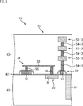
- FIG. 3 shows a part of a cross-sectional configuration of the pixel 21.
- the image sensor 11 is configured by laminating a wiring layer 43 via an insulating layer 42 on a semiconductor substrate 41 on which a PD 31, a diffusion layer 39 of the FD portion 33, and the like are formed.
- a diffusion layer 39 is formed by ion-implanting P-type impurities into an N-type silicon substrate.
- a gate electrode 51 constituting the transfer transistor 32 and a gate electrode 52 constituting the amplification transistor 34 are stacked on the semiconductor substrate 41.
- the semiconductor substrate 41 is formed with a diffusion layer serving as a drain and a source constituting the amplification transistor 34 and the selection transistor 35, similarly to the diffusion layer 39.
- the insulating layer 42 is formed, for example, by forming a thin film of silicon dioxide (SiO 2), and insulates the surface of the semiconductor substrate 41. Although not shown, an insulating layer is also formed between the semiconductor substrate 41 and the gate electrode 51 and the gate electrode 52.
- the wiring layer 43 is configured by stacking a plurality of layers of metal wiring 53 via an interlayer insulating film, and FIG. 3 shows a configuration example in which three layers of metal wirings 53-1 to 53-3 are stacked. It is shown.
- the metal wirings 53-1 to 53-3 are used for input / output of signals between the pixel 21 and the outside. For example, a drive signal is input to the pixel 21 via the metal wirings 53-1 to 53-3, and the pixel 21 The pixel signal obtained in is output via the metal wirings 53-1 to 53-3.
- the stacked metal wirings 53-1 to 53-3 are connected to each other through a contact wiring 54 formed so as to penetrate the interlayer insulating film.
- the metal wiring 53-1 is connected to the gate electrode 51 through the contact wiring 54-1
- the metal wiring 53-2 is connected to the metal wiring 53-1 through the contact wiring 54-2
- the metal wiring 53-3 is connected to the metal wiring 53-2 through the contact wiring 54-3.
- the diffusion layer 39 of the FD portion 33 is connected to the FD connection wiring 38 via the contact wiring 55, and the gate electrode 52 constituting the amplification transistor 34 is connected to the FD connection wiring via the contact wiring 56. 38.
- the contact wirings 55 and 56 are formed to extend in a direction perpendicular to the semiconductor substrate 41, and are formed to have a different height from the contact wiring 54-1 connected to the metal wiring 53-1.
- the FD connection wiring 38 is located closer to the semiconductor substrate 41 than the metal wirings 53-1 to 53-3 formed in the wiring layer 43, that is, lower than the first metal wiring 53-1. Formed. That is, the FD connection wiring 38 that connects the diffusion layer 39 and the gate electrode 52 is formed by forming a thinner interlayer insulating film before forming the metal wiring 53 used for connection at other locations. Is formed by forming a metal film on the substrate and performing sputtering. Thereafter, an interlayer insulating film is formed to a predetermined thickness to form a first layer metal wiring 53-1, and thereafter metal wirings 53-2 and 53-3 are formed in the same manner.
- the FD connection wiring 38 is formed to be a thin film having a thickness of 50 nm or less, for example.
- the FD connection wiring 38 can be formed of, for example, titanium (Ti), titanium nitride (TiN), tungsten (W), aluminum (Al), or copper (Cu). Further, the FD connection wiring 38 may be formed by a laminated structure (Ti / TiN / Ti) of titanium and titanium nitride, for example.
- the FD connection wiring 38 in the pixel 21 configured as described above, by forming the FD connection wiring 38 so as to be lower than the metal wiring 53-1, the storage capacity of the FD portion 33 can be reduced, and the amplification transistor The conversion efficiency in 34 can be made higher.
- the high conversion rate of the amplification transistor 34 can also be achieved by forming the FD connection wiring 38 to be a thin film.
- the FD connection wiring 38 has a layout that avoids overlapping with the gate electrodes of the transfer transistor 32 and the connection transistor 36 in a plan view. It is possible to prevent a capacitance from being generated between the FD connection wiring 38 and the gate electrode. Also by this, the storage capacity of the FD unit 33 can be reduced.
- the imaging device 11 has the pixel 21 configured so that the conversion efficiency in the amplification transistor 34 can be switched by the connection transistor 36, and effectively utilizes the effect of reducing the storage capacity of the FD unit 33. can do. That is, when the conversion efficiency of the amplification transistor 34 is a high conversion rate, there is a concern that the pixel signal is saturated when imaging is performed in a bright situation. On the other hand, in the imaging device 11, when imaging is performed in a bright situation, the connection transistor 36 can be turned on and the conversion efficiency in the amplification transistor 34 can be set to a low conversion rate, so that the pixel signal is saturated. Can be avoided.
- the imaging device 11 can capture a clear image with lower noise in an environment with low illuminance such as in the dark by setting the conversion efficiency of the amplification transistor 34 to a high conversion rate.
- the imaging device 11 captures an image with appropriate exposure without saturation of the pixel signal by switching the conversion efficiency of the amplification transistor 34 to be a low conversion rate in an environment with high illuminance such as daytime. can do.
- the image sensor 11 can capture a good image in any lighting environment, and is suitable for use in applications such as monitoring and vehicle mounting.
- the above-described image sensor of Patent Document 1 has a structure in which parasitic capacitance increases due to the proximity of the wiring connected to the FD unit to the substrate. In this structure, parasitic capacitance is generated. For this reason, it has been difficult for the conventional imaging device to achieve high conversion efficiency like the imaging device 11.
- the FD connection wiring 38 is formed with an appropriate interval by the contact wirings 55 and 56 to such an extent that a small parasitic capacitance is generated between the semiconductor substrate 41 and the FD connection wiring 38. .
- the FD connection wiring 38 and the metal wiring 53 are formed in different layers in the image pickup device 11, it is possible to avoid the generation of parasitic capacitance between these wirings. For this reason, the imaging device 11 can reduce the storage capacity of the FD unit 33 as compared with the conventional case, and as a result, can achieve high conversion efficiency in the amplification transistor 34.
- the FD connection wiring 38 forms a barrier metal so as not to perform a Schottky junction, the FD connection wiring 38 can be subjected to an ohmic junction, thereby reducing a capacitance generated between the semiconductor substrate 41 and the FD connection wiring 38.
- the driving method of the pixel 21 will be described with reference to FIG.
- FIG. 4 shows a timing chart of the selection signal SEL, the reset signal RST, the connection signal FDG, and the transfer signal TRG used for driving the pixel 21.
- the selection signal SEL In a state where the row in which the pixels 21 are arranged is not selected as a row for performing the shutter operation and the readout operation (hereinafter referred to as non-selection), the selection signal SEL, the reset signal RST, the connection signal FDG, and the transfer signal Each TRG is set to L level.
- the reset signal RST becomes H level for a predetermined period, and the connection signal is shorter than the predetermined period.
- FDG goes high.
- the FD portion 33 is connected to the drain power supply Vdd via the connection transistor 36 and the reset transistor 37, and the charge accumulated in the FD portion 33 is discharged to the drain power supply Vdd.
- the transfer signal TRG is at the H level in a pulsed manner, whereby the charge accumulated in the PD 31 is discharged, and the charge accumulation by the PD 31 is started.
- the pixels 21 that have become non-selected rows are in a state of accumulating charges generated in the PD 31.
- one horizontal period of a plurality of rows that is sequentially performed is represented by one single horizontal period.
- the selection signal SEL becomes H level for one horizontal period, and the amplification transistor 34 is connected to the vertical signal line 23 via the selection transistor 35.
- the reset signal RST becomes H level
- the connection signal FDG becomes H level in a pulse shape
- the FD unit 33 is reset
- the pixel signal at the reset level is read (P phase).
- the transfer signal TRG changes to the H level in a pulse shape, and the charge accumulated in the PD 31 is transferred to the FD unit 33, and the pixel signal at the data level is read (D phase).
- the selection signal SEL becomes H level for one horizontal period, and amplification is performed.
- the transistor 34 is connected to the vertical signal line 23 via the selection transistor 35. Thereafter, subsequent to the reset signal RST becoming H level, the connection signal FDG becomes H level, and the pixel signal at the reset level is read while the connection transistor 36 remains on (P phase).
- connection signal FDG is maintained at the H level
- the transfer signal TRG is changed to the H level in a pulsed manner
- the charge accumulated in the PD 31 is transferred to the FD unit 33, and the pixel signal at the data level is read (D Then, the connection signal FDG becomes L level.
- connection signal FDG becomes H level in a pulse shape and the FD unit 33 is reset, and then the connection transistor 36 is turned off, and the FD
- the P phase and the D phase are read with the storage capacity of the unit 33 being small.
- the connection transistor 36 is kept on, and the P phase and the D phase are read in a state where the storage capacity of the FD unit 33 is large.
- the pixel 21 can switch between a high conversion rate and a low conversion rate, and a pixel signal can be read with an appropriate conversion efficiency according to the exposure state. That is, the storage transistor of the FD section 33 is switched by the connection transistor 36 and the connection transistor 36 is turned on, so that the conversion efficiency in the amplification transistor 34 is set to a high conversion rate and the pixel signal is read out. By turning off the pixel signal, the conversion efficiency in the amplification transistor 34 can be set to a low conversion rate, and the pixel signal can be read out.
- the pixel 21 employing the FD connection wiring 38 as shown in FIG. 3 is not limited to a configuration in which the amplification factor of the amplification transistor 34 can be changed using the connection transistor 36. A structure without the transistor 36 may be employed.
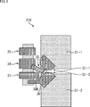
- FIG. 5A shows a circuit diagram of the pixel 21A
- FIG. 5B shows a planar configuration of the pixel 21A.
- the same reference numerals are given to the same components as those in the pixel 21 in FIG. 2, and the detailed description thereof is omitted.
- the pixel 21A includes a PD 31, a transfer transistor 32, an FD section 33, an amplification transistor 34, a selection transistor 35, and a reset transistor 37. That is, the pixel 21A has a configuration in which the connection transistor 36 is removed from the pixel 21 in FIG.
- the diffusion layer 39 of the FD portion 33 is connected to the gate electrode of the amplification transistor 34 via the FD connection wiring 38, and the FD connection wiring 38 is connected to the transfer transistor 32 or the reset transistor.
- the layout is made so as not to overlap with the gate electrode of the transistor 37 or the like.
- the pixel 21A has a structure (4Tr structure) including four transistors, that is, the transfer transistor 32, the amplification transistor 34, the selection transistor 35, and the reset transistor 37.
- the FD connection wiring 38 that connects the diffusion layer 39 of the FD section 33 and the gate electrode of the amplification transistor 34 has a lower layer than the metal wiring 53-1, as described with reference to FIG. Formed to be. Thereby, the pixel 21A can make the conversion efficiency in the amplification transistor 34 high conversion rate similarly to the pixel 21 of FIG.
- the pixel 21 may employ, for example, a structure (3Tr structure) including three transistors, that is, the transfer transistor 32, the amplification transistor 34, and the selection transistor 35 without including the selection transistor 35.
- a structure (3Tr structure) including three transistors, that is, the transfer transistor 32, the amplification transistor 34, and the selection transistor 35 without including the selection transistor 35.
- the pixel 21 employs a pixel sharing structure in which the FD unit 33, the amplification transistor 34, the selection transistor 35, and the reset transistor 37 are shared by a plurality of PDs 31. May be.
- FIG. 6 shows a planar configuration of the pixel 21B.
- the same reference numerals are given to the same components as those in the pixel 21 in FIG. 2, and detailed description thereof is omitted.
- the pixel 21B includes two PDs 31-1 and 31-2, two transfer transistors 32-1 and 32-2, an FD unit 33, an amplification transistor 34, a selection transistor 35, and a reset transistor 37. It is prepared for. That is, the pixel 21B adopts a two-pixel sharing structure in which the amplification transistor 34 and the like are shared by the two PDs 31-1 and 31-2.
- the FD connection wiring 38 ⁇ / b> B connects the diffusion layer 39 of the FD portion 33 and the gate electrode of the amplification transistor 34, and connects the diffusion layer 39 of the FD portion 33 and the source region of the reset transistor 37. Formed to connect.
- the FD connection wiring 38B is laid out so as not to overlap the gate electrodes of the transfer transistors 32-1 and 32-2, the reset transistor 37, and the like, like the FD connection wiring 38 of FIG.
- the FD connection wiring 38B is formed in a lower layer than the metal wiring 53-1, as described with reference to FIG. Thereby, the pixel 21B can make the conversion efficiency in the amplification transistor 34 a high conversion rate like the pixel 21 of FIG.
- FIG. 7 shows a planar configuration of the pixel 21C.
- the components common to the pixel 21 illustrated in FIG. 2 are denoted by the same reference numerals, and detailed description thereof is omitted.
- the pixel 21C includes four PDs 31-1 to 31-4, four transfer transistors 32-1 to 32-4, an FD unit 33, an amplification transistor 34, a selection transistor 35, and a reset transistor 37. It is prepared for. That is, the pixel 21C employs a four-pixel sharing structure in which the amplification transistor 34 and the like are shared by the four PDs 31-1 to 31-4.
- the FD connection wiring 38 ⁇ / b> C connects the diffusion layer 39 of the FD portion 33 and the gate electrode of the amplification transistor 34, and connects the diffusion layer 39 of the FD portion 33 and the source region of the reset transistor 37. Formed to connect.
- the FD connection wiring 38C is laid out so as not to overlap the gate electrodes of the transfer transistors 32-1 to 32-4, the reset transistor 37, and the like, like the FD connection wiring 38 of FIG.
- the FD connection wiring 38C is formed to be lower than the metal wiring 53-1, as described with reference to FIG. Thereby, the pixel 21C can make the conversion efficiency in the amplification transistor 34 a high conversion rate like the pixel 21 of FIG.
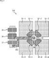
- FIG. 8A shows a circuit diagram of the pixel 21D
- FIG. 8B shows a planar configuration of the pixel 21D.
- the same reference numerals are given to the same components as those in the pixel 21 in FIG. 2, and the detailed description thereof is omitted.
- the pixel 21D includes a PD 31L, a PD 31S, two transfer transistors 32-1 and 32-2, an FD unit 33, an amplification transistor 34, a selection transistor 35, and two connection transistors 36-1 and 36. -2, a reset transistor 37, and a pixel capacitance 61.
- PD31L and PD31S are photoelectric conversion units having different sensitivities, and each incident light is converted into electric charge by photoelectric conversion and accumulated.
- the PD 31L is formed with a large area so as to have high sensitivity
- the PD 31S is formed with a small area so as to have low sensitivity.
- the transfer transistor 32-1 is driven according to the transfer signal TGL supplied from the vertical drive circuit 13. When the transfer transistor 32-1 is turned on, the charge accumulated in the PD 31L is transferred to the FD unit 33.
- the transfer transistor 32-2 is driven in accordance with the transfer signal TGS supplied from the vertical drive circuit 13. When the transfer transistor 32-2 is turned on, the charge accumulated in the PD 31S is transferred to the pixel internal capacitor 61.
- connection transistor 36-1 is formed so as to connect the FD unit 33 and the reset transistor 37, and can be driven according to the connection signal FDG supplied from the vertical drive circuit 13 to switch the storage capacitor of the FD unit 33.
- connection transistor 36-2 is formed so as to connect the in-pixel capacitance 61 to the connection point of the connection transistor 36-1 and the reset transistor 37.
- the connection transistor 36-2 is driven according to the connection signal FCG supplied from the vertical drive circuit 13, and when the connection transistor 36-2 is turned on, the charge accumulated in the pixel capacitance 61 causes the connection transistor 36-1 to be connected. To the FD unit 33.
- the intra-pixel capacitor 61 is a capacitor composed of, for example, two metal layers formed in the wiring layer 43 (see FIG. 3), and accumulates charges transferred from the PD 31S.
- the wiring 62 connected to the intra-pixel capacitor 61 and the wiring 63 connecting the connection transistor 36-2 and the diffusion layer between the connection transistor 36-1 and the reset transistor 37 are the metal wiring 53 of FIG. -1 to 53-3.
- the wirings 62 and 63 are also laid out so as not to overlap with the gate electrodes of other transistors in plan view.
- the FD connection wiring 38D connects the diffusion layer 39 of the FD section 33 and the gate electrode of the amplification transistor 34. Similarly to the FD connection wiring 38 of FIG. It is formed to be lower than -1. Thereby, the pixel 21D can make the conversion efficiency in the amplification transistor 34 high conversion rate similarly to the pixel 21 of FIG.
- the FD connection wiring 38D connected to the FD portion 33 to which charges are transferred from the highly sensitive PD 31L formed in a large area via the transfer transistor 32-1 is formed in a lower layer. Even in a low illuminance environment, noise generated in the pixel signal can be suppressed. That is, the image sensor 11 including the pixel 21D can capture a higher-sensitivity image by combining the characteristics of both high sensitivity by the PD 31L and high sensitivity by the FD connection wiring 38D. In addition, the imaging device 11 including the pixel 21D can perform imaging in a high illuminance environment by using the pixel signal obtained from the PD 31S to construct an image and avoiding saturation of the pixel signal.
- the image pickup device 11 including the pixel 21D can pick up a good image in both low and high illuminance environments.
- FIG. 9 shows a timing chart of the selection signal SEL, the connection signal FDG, the reset signal RST, the transfer signal TGS, the connection signal FCG, and the transfer signal TGL in each of the shutter row, readout row, and non-selected row.
- the horizontal synchronization signal XHS is a signal for synchronizing the operation in the row where the pixels 21D are arranged in one horizontal period.
- the connection signal FDG and the reset signal RST become H level in one horizontal period in which the row is driven.
- the FD portion 33 is connected to the drain power supply Vdd via the connection transistor 36-1 and the reset transistor 37, and the charge accumulated in the FD portion 33 is discharged to the drain power supply Vdd.
- connection signal FCG becomes H level
- the pixel capacitor 61 is connected to the drain power supply Vdd via the connection transistor 36-2 and the reset transistor 37, so that it is stored in the pixel capacitor 61.
- the electric charge is discharged to the drain power supply Vdd.
- the transfer signal TRS and the transfer signal TRL are changed to the H level in a pulse shape, the charges accumulated in the PD 31L and PD 31S are also discharged, and the accumulation of charges by the PD 31L and PD 31S is started.
- the reset signal RST becomes L level
- the connection signal FCG becomes L level
- the connection signal FDG becomes L level.
- the selection signal SEL is always at the L level.
- the selection signal SEL becomes H level
- the amplification transistor 34 is connected to the vertical signal line 23 via the selection transistor 35.
- the connection signal FDG becomes H level
- the FD section 33 is connected to the reset transistor 37.
- the transfer signal TGS is turned on in a pulse form at the same timing as the connection signal FCG becomes H level, and the PD 31S The accumulated charge is transferred to the pixel capacitor 61.
- connection signal FCG becomes L level
- the pixel internal capacity 61 is disconnected from the FD unit 33
- the reset signal RST becomes pulsed H level
- the FD unit 33 is reset
- the reset level pixel signal Is read (Large-PD P phase).
- the transfer signal TGL becomes H level in a pulse form, and the charge accumulated in the PD 31L is transferred to the FD unit 33 via the transfer transistor 32-1.
- a pixel signal having a data level corresponding to the charge generated in the PD 31L is read (Large-PD D phase).
- all of the horizontal synchronization signal XHS, the selection signal SEL, the connection signal FDG, the reset signal RST, the transfer signal TRS, the connection signal FCG, and the transfer signal TRL are always set to the L level.
- the pixel 21D can read out the pixel signal from the low-sensitivity PD 31S and read out the pixel signal from the high-sensitivity PD 31L. Therefore, the image sensor 11 including the pixel 21D uses the PD31L pixel signal in an exposure environment where the PD31L pixel signal is not saturated, and uses the PD31S pixel signal in an exposure environment where the PD31L pixel signal is saturated. A wide image can be constructed.
- the image sensor 11 having the pixel 21 of each embodiment as described above is, for example, an imaging system such as a digital still camera or a digital video camera, a mobile phone having an imaging function, or another having an imaging function.
- the present invention can be applied to various electronic devices such as these devices.
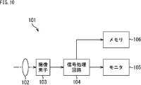
- FIG. 10 is a block diagram illustrating a configuration example of an imaging device mounted on an electronic device.
- the imaging apparatus 101 includes an optical system 102, an imaging element 103, a signal processing circuit 104, a monitor 105, and a memory 106, and can capture still images and moving images.
- the optical system 102 includes one or more lenses, guides image light (incident light) from a subject to the image sensor 103, and forms an image on a light receiving surface (sensor unit) of the image sensor 103.
- the image sensor 11 As the image sensor 103, the image sensor 11 having the pixel 21 of each embodiment described above is applied. In the image sensor 103, electrons are accumulated for a certain period according to an image formed on the light receiving surface via the optical system 102. Then, a signal corresponding to the electrons accumulated in the image sensor 103 is supplied to the signal processing circuit 104.
- the signal processing circuit 104 performs various signal processing on the pixel signal output from the image sensor 103.
- An image (image data) obtained by performing signal processing by the signal processing circuit 104 is supplied to the monitor 105 and displayed, or supplied to the memory 106 and stored (recorded).
- a clear image can be captured with lower noise by applying the imaging element 11 having the pixel 21 of each embodiment described above.
- FIG. 11 is a diagram showing a usage example in which the above-described image sensor is used.
- the image sensor described above can be used in various cases for sensing light such as visible light, infrared light, ultraviolet light, and X-ray as follows.
- Devices for taking images for viewing such as digital cameras and mobile devices with camera functions
- Devices used for traffic such as in-vehicle sensors that capture the back, surroundings, and interiors of vehicles, surveillance cameras that monitor traveling vehicles and roads, and ranging sensors that measure distances between vehicles, etc.
- Equipment used for home appliances such as TVs, refrigerators, air conditioners, etc. to take pictures and operate the equipment according to the gestures ⁇ Endoscopes, equipment that performs blood vessel photography by receiving infrared light, etc.
- Equipment used for medical and health care ⁇ Security equipment such as security surveillance cameras and personal authentication cameras ⁇ Skin measuring instrument for photographing skin and scalp photography Such as a microscope to do beauty Equipment used for sports-Equipment used for sports such as action cameras and wearable cameras for sports applications-Used for agriculture such as cameras for monitoring the condition of fields and crops apparatus
- this technique can also take the following structures.
- a photoelectric conversion unit that converts incident light into charges by photoelectric conversion and stores the charge; and A charge transfer unit that transfers the charge generated in the photoelectric conversion unit; A diffusion layer in which the charge is transferred through the charge transfer unit and having a predetermined storage capacity; A converter that converts the charge transferred to the diffusion layer into a pixel signal; A pixel having a connection layer connecting the diffusion layer and the conversion unit, The connection wiring is connected to the diffusion layer and the conversion unit via a contact wiring extending in a direction perpendicular to the semiconductor substrate on which the diffusion layer is formed, and the semiconductor is more than the other wiring provided in the pixel.
- An image sensor formed on the substrate side.
- the imaging device further includes a switching unit that switches a storage capacitor that stores the charge converted into the pixel signal by the conversion unit.
- the conversion efficiency in the transfer transistor is set to a high conversion rate, the pixel signal is read, and the storage unit is switched to a small capacity by the switching unit.
- the image pickup device according to (1) or (2), further including: a drive unit configured to read the pixel signal while setting a conversion efficiency in the transfer transistor to a low conversion rate.
- the connection wiring is formed in a thinner film than other wiring provided in the pixel.
- connection wiring is laid out so as not to overlap with a gate electrode of a transistor provided in the pixel in a plan view.
- connection wiring is formed of titanium, titanium nitride, tungsten, aluminum, copper, or a stacked structure of titanium and titanium nitride.
- a photoelectric conversion unit that converts incident light into charges by photoelectric conversion and accumulates the charge, a charge transfer unit that transfers the charge generated by the photoelectric conversion unit, and the charge is transferred via the charge transfer unit,
- a diffusion layer having a storage capacitor, a conversion unit that converts the charge transferred to the diffusion layer into a pixel signal, a connection wiring that connects the diffusion layer and the conversion unit, and the conversion unit that converts the pixel signal into the pixel signal.
- a switching unit that switches a storage capacitor that stores the charge to be converted, and the connection wiring is connected to the diffusion layer via a contact wiring that extends in a direction perpendicular to a semiconductor substrate on which the diffusion layer is formed.
- a driving method of an image sensor connected to the conversion unit and formed on the semiconductor substrate side with respect to other wiring provided in the pixel By switching the storage capacitor to a large capacity by the switching unit, the conversion efficiency in the transfer transistor is set to a high conversion rate, and the pixel signal is read.
- a driving method of reading the pixel signal by setting the conversion efficiency of the transfer transistor to a low conversion rate by switching the storage capacitor to a small capacity by the switching unit.
- a photoelectric conversion unit that converts incident light into charges by photoelectric conversion and stores the charge; and A charge transfer unit that transfers the charge generated in the photoelectric conversion unit; A diffusion layer in which the charge is transferred through the charge transfer unit and having a predetermined storage capacity; A converter that converts the charge transferred to the diffusion layer into a pixel signal; A pixel having a connection layer connecting the diffusion layer and the conversion unit; The connection wiring is connected to the diffusion layer and the conversion unit via a contact wiring extending in a direction perpendicular to the semiconductor substrate on which the diffusion layer is formed, and the semiconductor is more than the other wiring provided in the pixel.
- An electronic device including an image sensor formed on a substrate side.
- Incident light is converted into electric charge by photoelectric conversion and accumulated, and a plurality of photoelectric conversion units having different sensitivities from each other, A charge transfer unit that transfers the charge generated in the photoelectric conversion unit; A diffusion layer in which the charge is transferred through the charge transfer unit and having a predetermined storage capacity; A converter that converts the charge transferred to the diffusion layer into a pixel signal; A connection wiring connecting the diffusion layer and the conversion unit; An image sensor comprising: a pixel having a pixel internal capacitor that accumulates charges transferred from some of the photoelectric conversion units among the plurality of photoelectric conversion units.
- the imaging device further including a driving unit that sequentially reads pixel signals corresponding to charges generated in each of the plurality of photoelectric conversion units to the diffusion layer and reads the pixel signals.
- the connection wiring is connected to the diffusion layer and the conversion unit via a contact wiring extending in a direction perpendicular to the semiconductor substrate on which the diffusion layer is formed, and the semiconductor is more than the other wiring provided in the pixel.
- the imaging device according to (11) or (12), which is formed on a substrate side.
- the imaging device according to any one of (11) to (13), wherein the connection wiring is formed in a thinner film than other wiring provided in the pixel.
- connection wiring is laid out so as not to overlap with a gate electrode of a transistor provided in the pixel in a plan view.
- connection wiring is formed of titanium, titanium nitride, tungsten, aluminum, copper, or a stacked structure of titanium and titanium nitride.
- the incident light is converted into electric charge by photoelectric conversion and accumulated, and a plurality of photoelectric conversion units having different sensitivities, a charge transfer unit that transfers the charge generated in the photoelectric conversion unit, and the charge transfer unit A diffusion layer to which the charge is transferred and having a predetermined storage capacity; a conversion unit that converts the charge transferred to the diffusion layer into a pixel signal; a connection wiring that connects the diffusion layer and the conversion unit;
- the photoelectric conversion units a method for driving an imaging device including a pixel having a pixel internal capacity for accumulating charges transferred from some of the photoelectric conversion units, A driving method in which pixel signals corresponding to charges generated in each of the plurality of photoelectric conversion units are sequentially transferred to the diffusion layer to read out the pixel signals.
- Incident light is converted into electric charge by photoelectric conversion and accumulated, and a plurality of photoelectric conversion units having different sensitivities from each other,
- a charge transfer unit that transfers the charge generated in the photoelectric conversion unit;
- a diffusion layer in which the charge is transferred through the charge transfer unit and having a predetermined storage capacity;
- a converter that converts the charge transferred to the diffusion layer into a pixel signal;
- An electronic apparatus comprising an imaging device having a pixel having a pixel internal capacity for accumulating charges transferred from some of the photoelectric conversion units among the plurality of photoelectric conversion units.
Landscapes
- Engineering & Computer Science (AREA)
- Multimedia (AREA)
- Signal Processing (AREA)
- Solid State Image Pick-Up Elements (AREA)
- Transforming Light Signals Into Electric Signals (AREA)
Abstract
Description
・自動停止等の安全運転や、運転者の状態の認識等のために、自動車の前方や後方、周囲、車内等を撮影する車載用センサ、走行車両や道路を監視する監視カメラ、車両間等の測距を行う測距センサ等の、交通の用に供される装置
・ユーザのジェスチャを撮影して、そのジェスチャに従った機器操作を行うために、TVや、冷蔵庫、エアーコンディショナ等の家電に供される装置
・内視鏡や、赤外光の受光による血管撮影を行う装置等の、医療やヘルスケアの用に供される装置
・防犯用途の監視カメラや、人物認証用途のカメラ等の、セキュリティの用に供される装置
・肌を撮影する肌測定器や、頭皮を撮影するマイクロスコープ等の、美容の用に供される装置
・スポーツ用途等向けのアクションカメラやウェアラブルカメラ等の、スポーツの用に供される装置
・畑や作物の状態を監視するためのカメラ等の、農業の用に供される装置
(1)
入射した光を光電変換により電荷に変換して蓄積する光電変換部と、
前記光電変換部で発生した前記電荷を転送する電荷転送部と、
前記電荷転送部を介して前記電荷が転送され、所定の蓄積容量を備える拡散層と、
前記拡散層に転送された前記電荷を画素信号に変換する変換部と、
前記拡散層および前記変換部を接続する接続配線と
を有する画素を備え、
前記接続配線は、前記拡散層が形成される半導体基板に対して垂直方向に延びるコンタクト配線を介して前記拡散層および前記変換部に接続され、前記画素内に設けられる他の配線よりも前記半導体基板側に形成される
撮像素子。
(2)
前記画素は、前記変換部により前記画素信号に変換される前記電荷を蓄積する蓄積容量を切り替える切り替え部をさらに有する
上記(1)に記載の撮像素子。
(3)
前記切り替え部により前記蓄積容量を大容量に切り替えることにより、前記転送トランジスタにおける変換効率を高変換率に設定して前記画素信号の読み出しを行い
前記切り替え部により前記蓄積容量を小容量に切り替えることにより、前記転送トランジスタにおける変換効率を低変換率に設定して前記画素信号の読み出しを行う
駆動部をさらに備える
上記(1)または(2)に記載の撮像素子。
(4)
前記接続配線は、前記画素内に設けられる他の配線よりも薄膜に形成される
上記(1)から(3)までのいずれかに記載の撮像素子。
(5)
前記接続配線は、平面的に見て、前記画素内に設けられるトランジスタのゲート電極と重なることを回避してレイアウトされる
上記(1)から(4)までのいずれかに記載の撮像素子。
(6)
前記接続配線は、チタン、窒化チタン、タングステン、アルミニウム、または、銅、或いは、チタンおよび窒化チタンの積層構造により形成される
上記(1)から(5)までのいずれかに記載の撮像素子。
(7)
前記画素は、互いに感度の異なる複数の光電変換部を有する
上記(1)に記載の撮像素子。
(8)
複数の前記光電変換部それぞれで発生した電荷に応じた画素信号を、順次、前記拡散層に転送して前記画素信号の読み出しを行う駆動部をさらに備える
上記(7)に記載の撮像素子。
(9)
入射した光を光電変換により電荷に変換して蓄積する光電変換部と、前記光電変換部で発生した前記電荷を転送する電荷転送部と、前記電荷転送部を介して前記電荷が転送され、所定の蓄積容量を備える拡散層と、前記拡散層に転送された前記電荷を画素信号に変換する変換部と、前記拡散層および前記変換部を接続する接続配線と、前記変換部により前記画素信号に変換される前記電荷を蓄積する蓄積容量を切り替える切り替え部とを有する画素を備え、前記接続配線は、前記拡散層が形成される半導体基板に対して垂直方向に延びるコンタクト配線を介して前記拡散層および前記変換部に接続され、前記画素内に設けられる他の配線よりも前記半導体基板側に形成される撮像素子の駆動方法であって、
前記切り替え部により前記蓄積容量を大容量に切り替えることにより、前記転送トランジスタにおける変換効率を高変換率に設定して前記画素信号の読み出しを行い、
前記切り替え部により前記蓄積容量を小容量に切り替えることにより、前記転送トランジスタにおける変換効率を低変換率に設定して前記画素信号の読み出しを行う
駆動方法。
(10)
入射した光を光電変換により電荷に変換して蓄積する光電変換部と、
前記光電変換部で発生した前記電荷を転送する電荷転送部と、
前記電荷転送部を介して前記電荷が転送され、所定の蓄積容量を備える拡散層と、
前記拡散層に転送された前記電荷を画素信号に変換する変換部と、
前記拡散層および前記変換部を接続する接続配線と
を有する画素を有し、
前記接続配線は、前記拡散層が形成される半導体基板に対して垂直方向に延びるコンタクト配線を介して前記拡散層および前記変換部に接続され、前記画素内に設けられる他の配線よりも前記半導体基板側に形成される
撮像素子を備える電子機器。
(11)
入射した光を光電変換により電荷に変換して蓄積し、互いに感度の異なる複数の光電変換部と、
前記光電変換部で発生した前記電荷を転送する電荷転送部と、
前記電荷転送部を介して前記電荷が転送され、所定の蓄積容量を備える拡散層と、
前記拡散層に転送された前記電荷を画素信号に変換する変換部と、
前記拡散層および前記変換部を接続する接続配線と、
複数の前記光電変換部のうちの、一部の前記光電変換部から転送される電荷を蓄積する画素内容量と
を有する画素を備える撮像素子。
(12)
複数の前記光電変換部それぞれで発生した電荷に応じた画素信号を、順次、前記拡散層に転送して前記画素信号の読み出しを行う駆動部をさらに備える
上記(11)に記載の撮像素子。
(13)
前記接続配線は、前記拡散層が形成される半導体基板に対して垂直方向に延びるコンタクト配線を介して前記拡散層および前記変換部に接続され、前記画素内に設けられる他の配線よりも前記半導体基板側に形成される
上記(11)または(12)に記載の撮像素子。
(14)
前記接続配線は、前記画素内に設けられる他の配線よりも薄膜に形成される
上記(11)から(13)までのいずれかに記載の撮像素子。
(15)
前記接続配線は、平面的に見て、前記画素内に設けられるトランジスタのゲート電極と重なることを回避してレイアウトされる
上記(11)から(14)までのいずれかに記載の撮像素子。
(16)
前記接続配線は、チタン、窒化チタン、タングステン、アルミニウム、または、銅、或いは、チタンおよび窒化チタンの積層構造により形成される
上記(11)から(15)までのいずれかに記載の撮像素子。
(17)
入射した光を光電変換により電荷に変換して蓄積し、互いに感度の異なる複数の光電変換部と、前記光電変換部で発生した前記電荷を転送する電荷転送部と、前記電荷転送部を介して前記電荷が転送され、所定の蓄積容量を備える拡散層と、前記拡散層に転送された前記電荷を画素信号に変換する変換部と、前記拡散層および前記変換部を接続する接続配線と、複数の前記光電変換部のうちの、一部の前記光電変換部から転送される電荷を蓄積する画素内容量とを有する画素を備える撮像素子の駆動方法であって、
複数の前記光電変換部それぞれで発生した電荷に応じた画素信号を、順次、前記拡散層に転送して前記画素信号の読み出しを行う
駆動方法。
(18)
入射した光を光電変換により電荷に変換して蓄積し、互いに感度の異なる複数の光電変換部と、
前記光電変換部で発生した前記電荷を転送する電荷転送部と、
前記電荷転送部を介して前記電荷が転送され、所定の蓄積容量を備える拡散層と、
前記拡散層に転送された前記電荷を画素信号に変換する変換部と、
前記拡散層および前記変換部を接続する接続配線と、
複数の前記光電変換部のうちの、一部の前記光電変換部から転送される電荷を蓄積する画素内容量と
を有する画素を有する撮像素子を備える電子機器。
Claims (18)
- 入射した光を光電変換により電荷に変換して蓄積する光電変換部と、
前記光電変換部で発生した前記電荷を転送する電荷転送部と、
前記電荷転送部を介して前記電荷が転送され、所定の蓄積容量を備える拡散層と、
前記拡散層に転送された前記電荷を画素信号に変換する変換部と、
前記拡散層および前記変換部を接続する接続配線と
を有する画素を備え、
前記接続配線は、前記拡散層が形成される半導体基板に対して垂直方向に延びるコンタクト配線を介して前記拡散層および前記変換部に接続され、前記画素内に設けられる他の配線よりも前記半導体基板側に形成される
撮像素子。 - 前記画素は、前記変換部により前記画素信号に変換される前記電荷を蓄積する蓄積容量を切り替える切り替え部をさらに有する
請求項1に記載の撮像素子。 - 前記切り替え部により前記蓄積容量を大容量に切り替えることにより、前記転送トランジスタにおける変換効率を高変換率に設定して前記画素信号の読み出しを行い、
前記切り替え部により前記蓄積容量を小容量に切り替えることにより、前記転送トランジスタにおける変換効率を低変換率に設定して前記画素信号の読み出しを行う
駆動部をさらに備える
請求項1に記載の撮像素子。 - 前記接続配線は、前記画素内に設けられる他の配線よりも薄膜に形成される
請求項1に記載の撮像素子。 - 前記接続配線は、平面的に見て、前記画素内に設けられるトランジスタのゲート電極と重なることを回避してレイアウトされる
請求項1に記載の撮像素子。 - 前記接続配線は、チタン、窒化チタン、タングステン、アルミニウム、または、銅、或いは、チタンおよび窒化チタンの積層構造により形成される
請求項1に記載の撮像素子。 - 前記画素は、互いに感度の異なる複数の光電変換部を有する
請求項1に記載の撮像素子。 - 複数の前記光電変換部それぞれで発生した電荷に応じた画素信号を、順次、前記拡散層に転送して前記画素信号の読み出しを行う駆動部をさらに備える
請求項7に記載の撮像素子。 - 入射した光を光電変換により電荷に変換して蓄積する光電変換部と、前記光電変換部で発生した前記電荷を転送する電荷転送部と、前記電荷転送部を介して前記電荷が転送され、所定の蓄積容量を備える拡散層と、前記拡散層に転送された前記電荷を画素信号に変換する変換部と、前記拡散層および前記変換部を接続する接続配線と、前記変換部により前記画素信号に変換される前記電荷を蓄積する蓄積容量を切り替える切り替え部とを有する画素を備え、前記接続配線は、前記拡散層が形成される半導体基板に対して垂直方向に延びるコンタクト配線を介して前記拡散層および前記変換部に接続され、前記画素内に設けられる他の配線よりも前記半導体基板側に形成される撮像素子の駆動方法であって、
前記切り替え部により前記蓄積容量を大容量に切り替えることにより、前記転送トランジスタにおける変換効率を高変換率に設定して前記画素信号の読み出しを行い、
前記切り替え部により前記蓄積容量を小容量に切り替えることにより、前記転送トランジスタにおける変換効率を低変換率に設定して前記画素信号の読み出しを行う
駆動方法。 - 入射した光を光電変換により電荷に変換して蓄積する光電変換部と、
前記光電変換部で発生した前記電荷を転送する電荷転送部と、
前記電荷転送部を介して前記電荷が転送され、所定の蓄積容量を備える拡散層と、
前記拡散層に転送された前記電荷を画素信号に変換する変換部と、
前記拡散層および前記変換部を接続する接続配線と
を有する画素を有し、
前記接続配線は、前記拡散層が形成される半導体基板に対して垂直方向に延びるコンタクト配線を介して前記拡散層および前記変換部に接続され、前記画素内に設けられる他の配線よりも前記半導体基板側に形成される
撮像素子を備える電子機器。 - 入射した光を光電変換により電荷に変換して蓄積し、互いに感度の異なる複数の光電変換部と、
前記光電変換部で発生した前記電荷を転送する電荷転送部と、
前記電荷転送部を介して前記電荷が転送され、所定の蓄積容量を備える拡散層と、
前記拡散層に転送された前記電荷を画素信号に変換する変換部と、
前記拡散層および前記変換部を接続する接続配線と、
複数の前記光電変換部のうちの、一部の前記光電変換部から転送される電荷を蓄積する画素内容量と
を有する画素を備える撮像素子。 - 複数の前記光電変換部それぞれで発生した電荷に応じた画素信号を、順次、前記拡散層に転送して前記画素信号の読み出しを行う駆動部をさらに備える
請求項11に記載の撮像素子。 - 前記接続配線は、前記拡散層が形成される半導体基板に対して垂直方向に延びるコンタクト配線を介して前記拡散層および前記変換部に接続され、前記画素内に設けられる他の配線よりも前記半導体基板側に形成される
請求項11に記載の撮像素子。 - 前記接続配線は、前記画素内に設けられる他の配線よりも薄膜に形成される
請求項11に記載の撮像素子。 - 前記接続配線は、平面的に見て、前記画素内に設けられるトランジスタのゲート電極と重なることを回避してレイアウトされる
請求項11に記載の撮像素子。 - 前記接続配線は、チタン、窒化チタン、タングステン、アルミニウム、または、銅、或いは、チタンおよび窒化チタンの積層構造により形成される
請求項11に記載の撮像素子。 - 入射した光を光電変換により電荷に変換して蓄積し、互いに感度の異なる複数の光電変換部と、前記光電変換部で発生した前記電荷を転送する電荷転送部と、前記電荷転送部を介して前記電荷が転送され、所定の蓄積容量を備える拡散層と、前記拡散層に転送された前記電荷を画素信号に変換する変換部と、前記拡散層および前記変換部を接続する接続配線と、複数の前記光電変換部のうちの、一部の前記光電変換部から転送される電荷を蓄積する画素内容量とを有する画素を備える撮像素子の駆動方法であって、
複数の前記光電変換部それぞれで発生した電荷に応じた画素信号を、順次、前記拡散層に転送して前記画素信号の読み出しを行う
駆動方法。 - 入射した光を光電変換により電荷に変換して蓄積し、互いに感度の異なる複数の光電変換部と、
前記光電変換部で発生した前記電荷を転送する電荷転送部と、
前記電荷転送部を介して前記電荷が転送され、所定の蓄積容量を備える拡散層と、
前記拡散層に転送された前記電荷を画素信号に変換する変換部と、
前記拡散層および前記変換部を接続する接続配線と、
複数の前記光電変換部のうちの、一部の前記光電変換部から転送される電荷を蓄積する画素内容量と
を有する画素を有する撮像素子を備える電子機器。
Priority Applications (14)
| Application Number | Priority Date | Filing Date | Title |
|---|---|---|---|
| CN202411982208.8A CN119996863A (zh) | 2015-06-09 | 2016-05-26 | 光检测设备和电子装置 |
| CN202210146522.7A CN114584722B (zh) | 2015-06-09 | 2016-05-26 | 摄像设备和电子装置 |
| US15/578,761 US10728475B2 (en) | 2015-06-09 | 2016-05-26 | Imaging element, driving method, and electronic device |
| CN201680031983.2A CN107615488B (zh) | 2015-06-09 | 2016-05-26 | 摄像元件、驱动方法和电子设备 |
| CN202210146586.7A CN114520885B (zh) | 2015-06-09 | 2016-05-26 | 摄像设备和电子装置 |
| JP2017523571A JPWO2016199588A1 (ja) | 2015-06-09 | 2016-05-26 | 撮像素子および駆動方法、並びに電子機器 |
| KR1020177034702A KR102590610B1 (ko) | 2015-06-09 | 2016-05-26 | 촬상 소자 및 구동 방법, 및 전자 기기 |
| US15/849,448 US10341592B2 (en) | 2015-06-09 | 2017-12-20 | Imaging element, driving method, and electronic device |
| US16/401,853 US10721422B2 (en) | 2015-06-09 | 2019-05-02 | Imaging element, driving method, and electronic device |
| US16/903,735 US11252356B2 (en) | 2015-06-09 | 2020-06-17 | Imaging element, driving method, and electronic device |
| US17/364,227 US11470276B2 (en) | 2015-06-09 | 2021-06-30 | Imaging element, driving method, and electronic device |
| US17/839,772 US11778349B2 (en) | 2015-06-09 | 2022-06-14 | Imaging element, driving method, and electronic device |
| US18/237,160 US12047700B2 (en) | 2015-06-09 | 2023-08-23 | Imaging element, driving method, and electronic device |
| US18/774,505 US20240373146A1 (en) | 2015-06-09 | 2024-07-16 | Imaging element, driving method, and electronic device |
Applications Claiming Priority (2)
| Application Number | Priority Date | Filing Date | Title |
|---|---|---|---|
| JP2015116650 | 2015-06-09 | ||
| JP2015-116650 | 2015-06-09 |
Related Child Applications (2)
| Application Number | Title | Priority Date | Filing Date |
|---|---|---|---|
| US15/578,761 A-371-Of-International US10728475B2 (en) | 2015-06-09 | 2016-05-26 | Imaging element, driving method, and electronic device |
| US15/849,448 Continuation US10341592B2 (en) | 2015-06-09 | 2017-12-20 | Imaging element, driving method, and electronic device |
Publications (1)
| Publication Number | Publication Date |
|---|---|
| WO2016199588A1 true WO2016199588A1 (ja) | 2016-12-15 |
Family
ID=57503190
Family Applications (1)
| Application Number | Title | Priority Date | Filing Date |
|---|---|---|---|
| PCT/JP2016/065591 Ceased WO2016199588A1 (ja) | 2015-06-09 | 2016-05-26 | 撮像素子および駆動方法、並びに電子機器 |
Country Status (6)
| Country | Link |
|---|---|
| US (1) | US10728475B2 (ja) |
| JP (1) | JPWO2016199588A1 (ja) |
| KR (1) | KR102590610B1 (ja) |
| CN (4) | CN107615488B (ja) |
| TW (1) | TWI701819B (ja) |
| WO (1) | WO2016199588A1 (ja) |
Cited By (3)
| Publication number | Priority date | Publication date | Assignee | Title |
|---|---|---|---|---|
| WO2018168120A1 (ja) * | 2017-03-13 | 2018-09-20 | ソニーセミコンダクタソリューションズ株式会社 | 固体撮像装置、その駆動方法および電子機器 |
| CN110892710A (zh) * | 2017-08-10 | 2020-03-17 | 索尼半导体解决方案公司 | 摄像装置 |
| US12581766B2 (en) | 2021-08-03 | 2026-03-17 | Sony Semiconductor Solutions Corporation | Solid-state imaging device and electronic equipment |
Families Citing this family (20)
| Publication number | Priority date | Publication date | Assignee | Title |
|---|---|---|---|---|
| US10341592B2 (en) | 2015-06-09 | 2019-07-02 | Sony Semiconductor Solutions Corporation | Imaging element, driving method, and electronic device |
| JP2017163010A (ja) * | 2016-03-10 | 2017-09-14 | ソニー株式会社 | 撮像装置、電子機器 |
| CN117577652A (zh) * | 2017-06-02 | 2024-02-20 | 索尼半导体解决方案公司 | 固态摄像装置和电子设备 |
| CN108270981B (zh) * | 2017-12-19 | 2021-05-14 | 思特威(上海)电子科技股份有限公司 | 像素单元及其成像方法和成像装置 |
| CN111656511B (zh) * | 2018-04-04 | 2024-08-27 | 松下知识产权经营株式会社 | 电子设备 |
| JP7362198B2 (ja) * | 2018-07-18 | 2023-10-17 | ソニーセミコンダクタソリューションズ株式会社 | 受光素子、測距モジュール、および、電子機器 |
| JP7368371B2 (ja) * | 2018-09-19 | 2023-10-24 | ソニーセミコンダクタソリューションズ株式会社 | 固体撮像素子および電子機器 |
| EP3886183B1 (en) * | 2018-11-19 | 2023-06-14 | Panasonic Intellectual Property Management Co., Ltd. | Imaging device and imaging system |
| US12119359B2 (en) | 2018-12-20 | 2024-10-15 | Sony Semiconductor Solutions Corporation | Imaging device |
| WO2020234652A1 (en) * | 2019-05-21 | 2020-11-26 | Sony Semiconductor Solutions Corporation | Imaging devices with multi-phase gated time-of-flight pixels |
| US20220217289A1 (en) * | 2019-05-21 | 2022-07-07 | Sony Semiconductor Solutions Corporation | Dual mode imaging devices |
| US12155947B2 (en) * | 2019-06-26 | 2024-11-26 | Sony Semiconductor Solutions Corporation | Imaging device with capacitance switching |
| WO2021085171A1 (ja) * | 2019-10-30 | 2021-05-06 | ソニーセミコンダクタソリューションズ株式会社 | 受光素子、測距モジュール、および、電子機器 |
| JP6824363B1 (ja) * | 2019-10-30 | 2021-02-03 | 浜松ホトニクス株式会社 | イメージセンサ、及びイメージセンサの制御方法 |
| JP7531272B2 (ja) * | 2019-11-15 | 2024-08-09 | ソニーセミコンダクタソリューションズ株式会社 | 撮像装置 |
| US11362121B2 (en) * | 2020-01-28 | 2022-06-14 | Omnivision Technologies, Inc. | Light attenuation layer fabrication method and structure for image sensor |
| KR20220120049A (ko) | 2021-02-22 | 2022-08-30 | 삼성전자주식회사 | 이미지 센서 |
| KR102913462B1 (ko) * | 2021-04-19 | 2026-01-15 | 삼성전자주식회사 | 이미지 센서 |
| US12396282B2 (en) * | 2021-10-20 | 2025-08-19 | Samsung Electronics Co., Ltd. | Image sensor |
| US12426394B2 (en) * | 2022-09-23 | 2025-09-23 | Taiwan Semiconductor Manufacturing Company, Ltd. | CMOS image sensor |
Citations (11)
| Publication number | Priority date | Publication date | Assignee | Title |
|---|---|---|---|---|
| JP2000232216A (ja) * | 1998-12-31 | 2000-08-22 | Eastman Kodak Co | 配線されたフローティングディフュージョンと共通増幅器のあるアクティブピクセルセンサ |
| JP2006073732A (ja) * | 2004-09-01 | 2006-03-16 | Canon Inc | 固体撮像装置及び固体撮像システム |
| JP2006196668A (ja) * | 2005-01-13 | 2006-07-27 | Toshiba Corp | 半導体装置及びその製造方法 |
| JP2008041689A (ja) * | 2006-08-01 | 2008-02-21 | Canon Inc | 光電変換装置および光電変換装置を用いた撮像システム |
| US20090261443A1 (en) * | 2008-04-18 | 2009-10-22 | Hyun-Pil Noh | Shared-pixel-type image sensor and method of fabricating the same |
| JP2010206095A (ja) * | 2009-03-05 | 2010-09-16 | Sony Corp | 固体撮像装置とその製造方法、及び電子機器 |
| JP2011082768A (ja) * | 2009-10-06 | 2011-04-21 | Canon Inc | 固体撮像装置および撮像装置 |
| JP2013034045A (ja) * | 2011-08-01 | 2013-02-14 | Sony Corp | 固体撮像装置、撮像装置 |
| JP2013211832A (ja) * | 2012-03-01 | 2013-10-10 | Canon Inc | 撮像装置、撮像システム、撮像装置の駆動方法 |
| JP2014060573A (ja) * | 2012-09-18 | 2014-04-03 | Sony Corp | 固体撮像素子、制御方法、および電子機器 |
| JP2014217011A (ja) * | 2013-04-30 | 2014-11-17 | 株式会社ニコン | 固体撮像素子および撮像装置 |
Family Cites Families (49)
| Publication number | Priority date | Publication date | Assignee | Title |
|---|---|---|---|---|
| JPH11307756A (ja) * | 1998-02-20 | 1999-11-05 | Canon Inc | 光電変換装置および放射線読取装置 |
| JP3988189B2 (ja) * | 2002-11-20 | 2007-10-10 | ソニー株式会社 | 固体撮像装置 |
| US7075049B2 (en) * | 2003-06-11 | 2006-07-11 | Micron Technology, Inc. | Dual conversion gain imagers |
| US7542085B2 (en) * | 2003-11-26 | 2009-06-02 | Aptina Imaging Corporation | Image sensor with a capacitive storage node linked to transfer gate |
| EP1732134B1 (en) * | 2004-02-27 | 2012-10-24 | National University Corporation Tohoku Unversity | Solid-state imagine device, line sensor, optical sensor, and method for operating solid-state imaging device |
| JP4299697B2 (ja) * | 2004-03-04 | 2009-07-22 | シャープ株式会社 | 固体撮像装置 |
| US7091531B2 (en) * | 2004-04-07 | 2006-08-15 | Micron Technology, Inc. | High dynamic range pixel amplifier |
| JP2006186187A (ja) | 2004-12-28 | 2006-07-13 | Matsushita Electric Ind Co Ltd | 固体撮像装置およびその製造方法 |
| JP4497366B2 (ja) * | 2005-02-04 | 2010-07-07 | 国立大学法人東北大学 | 光センサおよび固体撮像装置 |
| JP4677258B2 (ja) * | 2005-03-18 | 2011-04-27 | キヤノン株式会社 | 固体撮像装置及びカメラ |
| US7821560B2 (en) * | 2005-04-07 | 2010-10-26 | Tohoku Universityu | Optical sensor, solid-state imaging device, and operating method of solid-state imaging device |
| US7718459B2 (en) * | 2005-04-15 | 2010-05-18 | Aptina Imaging Corporation | Dual conversion gain pixel using Schottky and ohmic contacts to the floating diffusion region and methods of fabrication and operation |
| US7432540B2 (en) * | 2005-08-01 | 2008-10-07 | Micron Technology, Inc. | Dual conversion gain gate and capacitor combination |
| US20070035649A1 (en) * | 2005-08-10 | 2007-02-15 | Micron Technology, Inc. | Image pixel reset through dual conversion gain gate |
| KR100775058B1 (ko) * | 2005-09-29 | 2007-11-08 | 삼성전자주식회사 | 픽셀 및 이를 이용한 이미지 센서, 그리고 상기 이미지센서를 포함하는 이미지 처리 시스템 |
| JP4155996B2 (ja) * | 2006-03-03 | 2008-09-24 | シャープ株式会社 | 増幅型固体撮像装置 |
| JP4467542B2 (ja) * | 2006-06-15 | 2010-05-26 | 日本テキサス・インスツルメンツ株式会社 | 固体撮像装置 |
| EP2942813B1 (en) * | 2006-08-09 | 2020-09-30 | Tohoku University | Optical sensor and solid-state imaging device |
| US8184191B2 (en) * | 2006-08-09 | 2012-05-22 | Tohoku University | Optical sensor and solid-state imaging device |
| JP2008205639A (ja) * | 2007-02-16 | 2008-09-04 | Texas Instr Japan Ltd | 固体撮像装置及びその動作方法 |
| JP5214904B2 (ja) * | 2007-04-12 | 2013-06-19 | ルネサスエレクトロニクス株式会社 | 固体撮像素子の製造方法 |
| JP2008277511A (ja) * | 2007-04-27 | 2008-11-13 | Fujifilm Corp | 撮像素子及び撮像装置 |
| JP2009038263A (ja) * | 2007-08-02 | 2009-02-19 | Sharp Corp | 固体撮像素子および電子情報機器 |
| US8077237B2 (en) * | 2007-10-16 | 2011-12-13 | Aptina Imaging Corporation | Method and apparatus for controlling dual conversion gain signal in imaging devices |
| JP5347283B2 (ja) * | 2008-03-05 | 2013-11-20 | ソニー株式会社 | 固体撮像装置およびその製造方法 |
| CN102017150B (zh) * | 2008-05-02 | 2016-08-03 | 佳能株式会社 | 固态成像装置 |
| JP5257176B2 (ja) * | 2009-03-18 | 2013-08-07 | ソニー株式会社 | 固体撮像装置、固体撮像装置の駆動方法および電子機器 |
| JP2011159757A (ja) * | 2010-01-29 | 2011-08-18 | Sony Corp | 固体撮像装置とその製造方法、固体撮像装置の駆動方法、及び電子機器 |
| JP2011204797A (ja) * | 2010-03-24 | 2011-10-13 | Sony Corp | 固体撮像装置とその製造方法、及び電子機器 |
| JP5126291B2 (ja) * | 2010-06-07 | 2013-01-23 | 株式会社ニコン | 固体撮像素子 |
| JP5511541B2 (ja) * | 2010-06-24 | 2014-06-04 | キヤノン株式会社 | 固体撮像装置及び固体撮像装置の駆動方法 |
| JP2012124318A (ja) * | 2010-12-08 | 2012-06-28 | Sony Corp | 固体撮像素子の製造方法、固体撮像素子、および電子機器 |
| JP5637384B2 (ja) * | 2010-12-15 | 2014-12-10 | ソニー株式会社 | 固体撮像素子および駆動方法、並びに電子機器 |
| TWI456990B (zh) * | 2011-04-08 | 2014-10-11 | 原相科技股份有限公司 | 高動態範圍影像感測電路及高動態範圍影像讀取方法 |
| CN102752559B (zh) * | 2011-04-18 | 2015-07-22 | 原相科技股份有限公司 | 高动态范围影像感测电路及高动态范围影像读取方法 |
| CN103493475B (zh) * | 2011-04-28 | 2017-03-08 | 松下知识产权经营株式会社 | 固体摄像装置以及使用了该固体摄像装置的摄像机系统 |
| JP5791571B2 (ja) * | 2011-08-02 | 2015-10-07 | キヤノン株式会社 | 撮像素子及び撮像装置 |
| EP2800356A1 (en) * | 2011-12-27 | 2014-11-05 | Sony Corporation | Image pickup element, image pickup apparatus, electronic device, and image pickup method |
| US20130256510A1 (en) * | 2012-03-29 | 2013-10-03 | Omnivision Technologies, Inc. | Imaging device with floating diffusion switch |
| JP2014112580A (ja) | 2012-12-05 | 2014-06-19 | Sony Corp | 固体撮像素子および駆動方法 |
| JP2013254805A (ja) * | 2012-06-06 | 2013-12-19 | Sony Corp | 固体撮像素子及びその制御方法、並びに電子機器 |
| JP2014022795A (ja) * | 2012-07-13 | 2014-02-03 | Sony Corp | 撮像素子、撮像方法 |
| US9620558B2 (en) * | 2012-10-19 | 2017-04-11 | Nikon Corporation | Solid-state image sensor |
| US9659991B2 (en) * | 2012-10-22 | 2017-05-23 | Canon Kabushiki Kaisha | Image capturing apparatus, manufacturing method thereof, and camera |
| JP6161258B2 (ja) * | 2012-11-12 | 2017-07-12 | キヤノン株式会社 | 固体撮像装置およびその製造方法ならびにカメラ |
| KR102009192B1 (ko) * | 2013-02-05 | 2019-08-09 | 삼성전자주식회사 | 이미지 센서의 단위 픽셀 및 이를 포함하는 이미지 센서 |
| JP5813047B2 (ja) * | 2013-04-26 | 2015-11-17 | キヤノン株式会社 | 撮像装置、および、撮像システム。 |
| CN104135633A (zh) * | 2014-08-25 | 2014-11-05 | 北京思比科微电子技术股份有限公司 | 可变转换增益的图像传感器像素及其工作方法 |
| KR102730555B1 (ko) * | 2015-01-29 | 2024-11-15 | 소니 세미컨덕터 솔루션즈 가부시키가이샤 | 고체 촬상 소자 및 전자 기기 |
-
2016
- 2016-04-15 TW TW105111895A patent/TWI701819B/zh active
- 2016-05-26 JP JP2017523571A patent/JPWO2016199588A1/ja active Pending
- 2016-05-26 CN CN201680031983.2A patent/CN107615488B/zh active Active
- 2016-05-26 CN CN202411982208.8A patent/CN119996863A/zh active Pending
- 2016-05-26 CN CN202210146522.7A patent/CN114584722B/zh active Active
- 2016-05-26 WO PCT/JP2016/065591 patent/WO2016199588A1/ja not_active Ceased
- 2016-05-26 US US15/578,761 patent/US10728475B2/en active Active
- 2016-05-26 KR KR1020177034702A patent/KR102590610B1/ko active Active
- 2016-05-26 CN CN202210146586.7A patent/CN114520885B/zh active Active
Patent Citations (11)
| Publication number | Priority date | Publication date | Assignee | Title |
|---|---|---|---|---|
| JP2000232216A (ja) * | 1998-12-31 | 2000-08-22 | Eastman Kodak Co | 配線されたフローティングディフュージョンと共通増幅器のあるアクティブピクセルセンサ |
| JP2006073732A (ja) * | 2004-09-01 | 2006-03-16 | Canon Inc | 固体撮像装置及び固体撮像システム |
| JP2006196668A (ja) * | 2005-01-13 | 2006-07-27 | Toshiba Corp | 半導体装置及びその製造方法 |
| JP2008041689A (ja) * | 2006-08-01 | 2008-02-21 | Canon Inc | 光電変換装置および光電変換装置を用いた撮像システム |
| US20090261443A1 (en) * | 2008-04-18 | 2009-10-22 | Hyun-Pil Noh | Shared-pixel-type image sensor and method of fabricating the same |
| JP2010206095A (ja) * | 2009-03-05 | 2010-09-16 | Sony Corp | 固体撮像装置とその製造方法、及び電子機器 |
| JP2011082768A (ja) * | 2009-10-06 | 2011-04-21 | Canon Inc | 固体撮像装置および撮像装置 |
| JP2013034045A (ja) * | 2011-08-01 | 2013-02-14 | Sony Corp | 固体撮像装置、撮像装置 |
| JP2013211832A (ja) * | 2012-03-01 | 2013-10-10 | Canon Inc | 撮像装置、撮像システム、撮像装置の駆動方法 |
| JP2014060573A (ja) * | 2012-09-18 | 2014-04-03 | Sony Corp | 固体撮像素子、制御方法、および電子機器 |
| JP2014217011A (ja) * | 2013-04-30 | 2014-11-17 | 株式会社ニコン | 固体撮像素子および撮像装置 |
Cited By (8)
| Publication number | Priority date | Publication date | Assignee | Title |
|---|---|---|---|---|
| WO2018168120A1 (ja) * | 2017-03-13 | 2018-09-20 | ソニーセミコンダクタソリューションズ株式会社 | 固体撮像装置、その駆動方法および電子機器 |
| US10880505B2 (en) | 2017-03-13 | 2020-12-29 | Sony Semiconductor Solutions Corporation | Solid state imaging device, driving method of solid state imaging device, and electronic device |
| CN110892710A (zh) * | 2017-08-10 | 2020-03-17 | 索尼半导体解决方案公司 | 摄像装置 |
| US11289528B2 (en) | 2017-08-10 | 2022-03-29 | Sony Semiconductor Solutions Corporation | Imaging apparatus |
| CN110892710B (zh) * | 2017-08-10 | 2022-06-14 | 索尼半导体解决方案公司 | 摄像装置 |
| US11610931B2 (en) | 2017-08-10 | 2023-03-21 | Sony Semiconductor Solutions Corporation | Imaging apparatus |
| US11948963B2 (en) | 2017-08-10 | 2024-04-02 | Sony Semiconductor Solutions Corporation | Imaging apparatus |
| US12581766B2 (en) | 2021-08-03 | 2026-03-17 | Sony Semiconductor Solutions Corporation | Solid-state imaging device and electronic equipment |
Also Published As
| Publication number | Publication date |
|---|---|
| CN114584722A (zh) | 2022-06-03 |
| TWI701819B (zh) | 2020-08-11 |
| CN107615488A (zh) | 2018-01-19 |
| KR102590610B1 (ko) | 2023-10-18 |
| CN114520885A (zh) | 2022-05-20 |
| CN107615488B (zh) | 2022-03-18 |
| TW201644043A (zh) | 2016-12-16 |
| KR20180016369A (ko) | 2018-02-14 |
| CN119996863A (zh) | 2025-05-13 |
| JPWO2016199588A1 (ja) | 2018-03-29 |
| CN114520885B (zh) | 2023-12-15 |
| US10728475B2 (en) | 2020-07-28 |
| CN114584722B (zh) | 2024-12-17 |
| US20180184025A1 (en) | 2018-06-28 |
Similar Documents
| Publication | Publication Date | Title |
|---|---|---|
| US12047700B2 (en) | Imaging element, driving method, and electronic device | |
| CN107615488B (zh) | 摄像元件、驱动方法和电子设备 | |
| JP7745178B2 (ja) | 撮像装置 | |
| US9866771B2 (en) | Solid-state imaging device, signal processing method of solid-state imaging device, and electronic apparatus | |
| CN101656820B (zh) | 固体摄像装置及其制造方法 | |
| KR101696463B1 (ko) | 고체 촬상 장치, 고체 촬상 장치의 신호 처리 방법 및 촬상 장치 | |
| JP6922889B2 (ja) | 固体撮像素子、駆動方法、および電子機器 | |
| JP6873905B2 (ja) | 固体撮像装置および電子機器 | |
| JP6026102B2 (ja) | 固体撮像素子および電子機器 | |
| JPWO2017014025A1 (ja) | 撮像素子、製造方法、半導体装置、および電子機器 | |
| JP6907944B2 (ja) | 固体撮像素子及び電子機器 | |
| WO2016158483A1 (ja) | 固体撮像素子、駆動方法、および電子機器 | |
| JP2023068696A (ja) | 撮像素子および電子機器 |
Legal Events
| Date | Code | Title | Description |
|---|---|---|---|
| 121 | Ep: the epo has been informed by wipo that ep was designated in this application |
Ref document number: 16807295 Country of ref document: EP Kind code of ref document: A1 |
|
| ENP | Entry into the national phase |
Ref document number: 2017523571 Country of ref document: JP Kind code of ref document: A |
|
| ENP | Entry into the national phase |
Ref document number: 20177034702 Country of ref document: KR Kind code of ref document: A |
|
| WWE | Wipo information: entry into national phase |
Ref document number: 15578761 Country of ref document: US |
|
| NENP | Non-entry into the national phase |
Ref country code: DE |
|
| 122 | Ep: pct application non-entry in european phase |
Ref document number: 16807295 Country of ref document: EP Kind code of ref document: A1 |