WO2016199556A1 - メモリデバイスおよびメモリシステム - Google Patents
メモリデバイスおよびメモリシステム Download PDFInfo
- Publication number
- WO2016199556A1 WO2016199556A1 PCT/JP2016/064772 JP2016064772W WO2016199556A1 WO 2016199556 A1 WO2016199556 A1 WO 2016199556A1 JP 2016064772 W JP2016064772 W JP 2016064772W WO 2016199556 A1 WO2016199556 A1 WO 2016199556A1
- Authority
- WO
- WIPO (PCT)
- Prior art keywords
- memory cell
- electrode
- electrodes
- memory
- memory device
- Prior art date
- Legal status (The legal status is an assumption and is not a legal conclusion. Google has not performed a legal analysis and makes no representation as to the accuracy of the status listed.)
- Ceased
Links
Images

















Classifications
-
- H—ELECTRICITY
- H10—SEMICONDUCTOR DEVICES; ELECTRIC SOLID-STATE DEVICES NOT OTHERWISE PROVIDED FOR
- H10B—ELECTRONIC MEMORY DEVICES
- H10B41/00—Electrically erasable-and-programmable ROM [EEPROM] devices comprising floating gates
- H10B41/20—Electrically erasable-and-programmable ROM [EEPROM] devices comprising floating gates characterised by three-dimensional [3D] arrangements, e.g. with cells on different height levels
-
- H—ELECTRICITY
- H10—SEMICONDUCTOR DEVICES; ELECTRIC SOLID-STATE DEVICES NOT OTHERWISE PROVIDED FOR
- H10B—ELECTRONIC MEMORY DEVICES
- H10B63/00—Resistance change memory devices, e.g. resistive RAM [ReRAM] devices
- H10B63/80—Arrangements comprising multiple bistable or multi-stable switching components of the same type on a plane parallel to the substrate, e.g. cross-point arrays
- H10B63/84—Arrangements comprising multiple bistable or multi-stable switching components of the same type on a plane parallel to the substrate, e.g. cross-point arrays arranged in a direction perpendicular to the substrate, e.g. 3D cell arrays
- H10B63/845—Arrangements comprising multiple bistable or multi-stable switching components of the same type on a plane parallel to the substrate, e.g. cross-point arrays arranged in a direction perpendicular to the substrate, e.g. 3D cell arrays the switching components being connected to a common vertical conductor
-
- G—PHYSICS
- G11—INFORMATION STORAGE
- G11C—STATIC STORES
- G11C29/00—Checking stores for correct operation ; Subsequent repair; Testing stores during standby or offline operation
- G11C29/70—Masking faults in memories by using spares or by reconfiguring
- G11C29/78—Masking faults in memories by using spares or by reconfiguring using programmable devices
- G11C29/80—Masking faults in memories by using spares or by reconfiguring using programmable devices with improved layout
-
- H—ELECTRICITY
- H10—SEMICONDUCTOR DEVICES; ELECTRIC SOLID-STATE DEVICES NOT OTHERWISE PROVIDED FOR
- H10B—ELECTRONIC MEMORY DEVICES
- H10B41/00—Electrically erasable-and-programmable ROM [EEPROM] devices comprising floating gates
- H10B41/30—Electrically erasable-and-programmable ROM [EEPROM] devices comprising floating gates characterised by the memory core region
-
- H—ELECTRICITY
- H10—SEMICONDUCTOR DEVICES; ELECTRIC SOLID-STATE DEVICES NOT OTHERWISE PROVIDED FOR
- H10B—ELECTRONIC MEMORY DEVICES
- H10B43/00—EEPROM devices comprising charge-trapping gate insulators
- H10B43/20—EEPROM devices comprising charge-trapping gate insulators characterised by three-dimensional [3D] arrangements, e.g. with cells on different height levels
-
- H—ELECTRICITY
- H10—SEMICONDUCTOR DEVICES; ELECTRIC SOLID-STATE DEVICES NOT OTHERWISE PROVIDED FOR
- H10B—ELECTRONIC MEMORY DEVICES
- H10B43/00—EEPROM devices comprising charge-trapping gate insulators
- H10B43/30—EEPROM devices comprising charge-trapping gate insulators characterised by the memory core region
-
- H—ELECTRICITY
- H10—SEMICONDUCTOR DEVICES; ELECTRIC SOLID-STATE DEVICES NOT OTHERWISE PROVIDED FOR
- H10B—ELECTRONIC MEMORY DEVICES
- H10B61/00—Magnetic memory devices, e.g. magnetoresistive RAM [MRAM] devices
- H10B61/20—Magnetic memory devices, e.g. magnetoresistive RAM [MRAM] devices comprising components having three or more electrodes, e.g. transistors
-
- H—ELECTRICITY
- H10—SEMICONDUCTOR DEVICES; ELECTRIC SOLID-STATE DEVICES NOT OTHERWISE PROVIDED FOR
- H10B—ELECTRONIC MEMORY DEVICES
- H10B61/00—Magnetic memory devices, e.g. magnetoresistive RAM [MRAM] devices
- H10B61/20—Magnetic memory devices, e.g. magnetoresistive RAM [MRAM] devices comprising components having three or more electrodes, e.g. transistors
- H10B61/22—Magnetic memory devices, e.g. magnetoresistive RAM [MRAM] devices comprising components having three or more electrodes, e.g. transistors of the field-effect transistor [FET] type
-
- H—ELECTRICITY
- H10—SEMICONDUCTOR DEVICES; ELECTRIC SOLID-STATE DEVICES NOT OTHERWISE PROVIDED FOR
- H10N—ELECTRIC SOLID-STATE DEVICES NOT OTHERWISE PROVIDED FOR
- H10N70/00—Solid-state devices having no potential barriers, and specially adapted for rectifying, amplifying, oscillating or switching
- H10N70/20—Multistable switching devices, e.g. memristors
-
- H—ELECTRICITY
- H10—SEMICONDUCTOR DEVICES; ELECTRIC SOLID-STATE DEVICES NOT OTHERWISE PROVIDED FOR
- H10N—ELECTRIC SOLID-STATE DEVICES NOT OTHERWISE PROVIDED FOR
- H10N70/00—Solid-state devices having no potential barriers, and specially adapted for rectifying, amplifying, oscillating or switching
- H10N70/20—Multistable switching devices, e.g. memristors
- H10N70/231—Multistable switching devices, e.g. memristors based on solid-state phase change, e.g. between amorphous and crystalline phases, Ovshinsky effect
-
- H—ELECTRICITY
- H10—SEMICONDUCTOR DEVICES; ELECTRIC SOLID-STATE DEVICES NOT OTHERWISE PROVIDED FOR
- H10N—ELECTRIC SOLID-STATE DEVICES NOT OTHERWISE PROVIDED FOR
- H10N70/00—Solid-state devices having no potential barriers, and specially adapted for rectifying, amplifying, oscillating or switching
- H10N70/801—Constructional details of multistable switching devices
- H10N70/821—Device geometry
-
- H—ELECTRICITY
- H10—SEMICONDUCTOR DEVICES; ELECTRIC SOLID-STATE DEVICES NOT OTHERWISE PROVIDED FOR
- H10N—ELECTRIC SOLID-STATE DEVICES NOT OTHERWISE PROVIDED FOR
- H10N70/00—Solid-state devices having no potential barriers, and specially adapted for rectifying, amplifying, oscillating or switching
- H10N70/801—Constructional details of multistable switching devices
- H10N70/841—Electrodes
-
- H—ELECTRICITY
- H10—SEMICONDUCTOR DEVICES; ELECTRIC SOLID-STATE DEVICES NOT OTHERWISE PROVIDED FOR
- H10W—GENERIC PACKAGES, INTERCONNECTIONS, CONNECTORS OR OTHER CONSTRUCTIONAL DETAILS OF DEVICES COVERED BY CLASS H10
- H10W20/00—Interconnections in chips, wafers or substrates
- H10W20/40—Interconnections external to wafers or substrates, e.g. back-end-of-line [BEOL] metallisations or vias connecting to gate electrodes
- H10W20/41—Interconnections external to wafers or substrates, e.g. back-end-of-line [BEOL] metallisations or vias connecting to gate electrodes characterised by their conductive parts
- H10W20/43—Layouts of interconnections
-
- H—ELECTRICITY
- H10—SEMICONDUCTOR DEVICES; ELECTRIC SOLID-STATE DEVICES NOT OTHERWISE PROVIDED FOR
- H10D—INORGANIC ELECTRIC SEMICONDUCTOR DEVICES
- H10D88/00—Three-dimensional [3D] integrated devices
-
- H—ELECTRICITY
- H10—SEMICONDUCTOR DEVICES; ELECTRIC SOLID-STATE DEVICES NOT OTHERWISE PROVIDED FOR
- H10N—ELECTRIC SOLID-STATE DEVICES NOT OTHERWISE PROVIDED FOR
- H10N70/00—Solid-state devices having no potential barriers, and specially adapted for rectifying, amplifying, oscillating or switching
- H10N70/20—Multistable switching devices, e.g. memristors
- H10N70/24—Multistable switching devices, e.g. memristors based on migration or redistribution of ionic species, e.g. anions, vacancies
- H10N70/245—Multistable switching devices, e.g. memristors based on migration or redistribution of ionic species, e.g. anions, vacancies the species being metal cations, e.g. programmable metallization cells
-
- H—ELECTRICITY
- H10—SEMICONDUCTOR DEVICES; ELECTRIC SOLID-STATE DEVICES NOT OTHERWISE PROVIDED FOR
- H10N—ELECTRIC SOLID-STATE DEVICES NOT OTHERWISE PROVIDED FOR
- H10N70/00—Solid-state devices having no potential barriers, and specially adapted for rectifying, amplifying, oscillating or switching
- H10N70/801—Constructional details of multistable switching devices
- H10N70/821—Device geometry
- H10N70/823—Device geometry adapted for essentially horizontal current flow, e.g. bridge type devices
-
- H—ELECTRICITY
- H10—SEMICONDUCTOR DEVICES; ELECTRIC SOLID-STATE DEVICES NOT OTHERWISE PROVIDED FOR
- H10N—ELECTRIC SOLID-STATE DEVICES NOT OTHERWISE PROVIDED FOR
- H10N70/00—Solid-state devices having no potential barriers, and specially adapted for rectifying, amplifying, oscillating or switching
- H10N70/801—Constructional details of multistable switching devices
- H10N70/841—Electrodes
- H10N70/8416—Electrodes adapted for supplying ionic species
-
- H—ELECTRICITY
- H10—SEMICONDUCTOR DEVICES; ELECTRIC SOLID-STATE DEVICES NOT OTHERWISE PROVIDED FOR
- H10N—ELECTRIC SOLID-STATE DEVICES NOT OTHERWISE PROVIDED FOR
- H10N70/00—Solid-state devices having no potential barriers, and specially adapted for rectifying, amplifying, oscillating or switching
- H10N70/801—Constructional details of multistable switching devices
- H10N70/881—Switching materials
- H10N70/883—Oxides or nitrides
-
- H—ELECTRICITY
- H10—SEMICONDUCTOR DEVICES; ELECTRIC SOLID-STATE DEVICES NOT OTHERWISE PROVIDED FOR
- H10N—ELECTRIC SOLID-STATE DEVICES NOT OTHERWISE PROVIDED FOR
- H10N70/00—Solid-state devices having no potential barriers, and specially adapted for rectifying, amplifying, oscillating or switching
- H10N70/801—Constructional details of multistable switching devices
- H10N70/881—Switching materials
- H10N70/883—Oxides or nitrides
- H10N70/8833—Binary metal oxides, e.g. TaOx
Definitions
- the present disclosure relates to a memory device and a memory system including a plurality of nonvolatile storage units.
- JP 2011-222994 A International Publication 2012/070236 Specification JP 2011-1114011 A
- a memory device includes n memory cell units stacked in order from the first to the n-th in the first direction on a substrate.
- Each of these n memory cell units includes one or more first electrodes, a plurality of second electrodes provided so as to intersect with each of the first electrodes, one or more first electrodes, and a plurality of second electrodes.
- a plurality of memory cells provided at respective intersections with the electrodes and respectively connected to both the first electrode and the second electrode; and one or more memory cells connected to the first electrode to form one or more connection portions And a lead wire.
- connection portion in the (m + 1) th (m is a natural number equal to or less than n) memory cell unit is an mth memory cell region surrounded by a plurality of memory cells in the mth memory cell unit. It is in the position which overlaps in the 1st direction. That is, this memory device is configured such that the projection image of the mth memory cell region in the first direction and the projection image of the connection portion in the (m + 1) th memory cell unit in the first direction overlap. Has been.
- a memory system as an embodiment of the present disclosure includes the memory device described above and a control unit that controls the memory device.
- connection portion in the (m + 1) th memory cell unit is provided at a position overlapping the memory cell region in the mth memory cell unit. Yes. Therefore, the entire memory device can have more memory cells in a predetermined space.
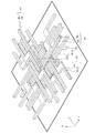
- FIG. 1 is a perspective view illustrating an overall configuration example of a memory device according to a first embodiment of the present disclosure.
- FIG. 2 is an equivalent circuit diagram illustrating a part of the memory device illustrated in FIG. 1.
- FIG. 2 is an enlarged perspective view illustrating an example of a selection transistor applied to the memory device illustrated in FIG. 1 in an enlarged manner.
- FIG. 2 is an enlarged perspective view showing an enlarged memory cell applied to the memory device shown in FIG. 1 and an equivalent circuit diagram thereof.
- FIG. 4 is an enlarged perspective view showing another memory cell applied to the memory device shown in FIG. 1 and an equivalent circuit diagram thereof.
- FIG. 3 is a perspective view illustrating a step in the method for manufacturing the memory device illustrated in FIG. 1. It is sectional drawing showing the 1 process following FIG. 5A.
- FIG. 5A FIG.
- FIG. 5C is a cross-sectional view illustrating a process following FIG. 5B. It is sectional drawing showing the 1 process following FIG. 5C. It is sectional drawing showing the 1 process following FIG. 5D.
- FIG. 28 is a perspective view illustrating a first modification example of the memory device according to the first embodiment of the disclosure.
- FIG. 7 is an equivalent circuit diagram illustrating a part of the memory device illustrated in FIG. 6.
- FIG. 7 is an enlarged perspective view illustrating an example of a memory cell applied to the memory device illustrated in FIG. 6 in an enlarged manner.
- FIG. 7 is a perspective view illustrating a part of the memory device illustrated in FIG. 6.
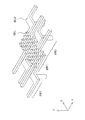
- 12 is a perspective view illustrating a second modification example of the memory device according to the first embodiment of the disclosure.
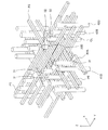
- FIG. 3 is a perspective view illustrating an overall configuration example of a memory device according to a second embodiment of the present disclosure.
- FIG. FIG. 12 is an enlarged perspective view illustrating an enlarged memory cell applied to the memory device illustrated in FIG. 11 and an equivalent circuit diagram thereof.
- FIG. 12 is a cross-sectional view schematically showing a cross-section of the main part of the memory device shown in FIG. 11.
- FIG. 12 is a perspective view illustrating a step in the method for manufacturing the memory device illustrated in FIG. 11. It is sectional drawing showing the 1 process following FIG. 14A. It is sectional drawing showing the 1 process following FIG. 14B.
- FIG. 14C is a cross-sectional view illustrating a process following FIG. 14C. It is sectional drawing showing the 1 process following FIG. 14D.
- FIG. 14F is a cross-sectional view illustrating a process following FIG. 14F. It is sectional drawing showing the 1 process following FIG. 14G.
- FIG. 14F is a cross-sectional view illustrating a process following FIG. 14H.
- FIG. 14D is a cross-sectional view illustrating a process following FIG. 14J.
- FIG. 14D is a cross-sectional view illustrating a process following FIG. 14K.
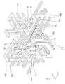
- FIG. 14 is a perspective view illustrating an overall configuration example of a memory device according to a third embodiment of the present disclosure.
- FIG. 16 is an enlarged perspective view illustrating an enlarged memory cell applied to the memory device shown in FIG. 15 and an equivalent circuit diagram thereof.
- FIG. 16 is an enlarged perspective view illustrating an enlarged memory cell applied to the memory device shown in FIG. 15 and an equivalent circuit diagram thereof.
- FIG. 16 is a perspective view illustrating a process in a method for manufacturing the memory device illustrated in FIG. 15.
- FIG. 17B is a cross-sectional view illustrating a process following FIG. 17A.
- FIG. 17B is a cross-sectional view illustrating a process following FIG. 17B.
- FIG. 17D is a cross-sectional view illustrating a process following FIG. 17C.
- FIG. 17D is a cross-sectional view illustrating a process following FIG. 17D.
- FIG. 17D is a cross-sectional view illustrating a process following FIG. 17F.
- FIG. 16 is a cross sectional view schematically showing a cross section of a main part of the memory device shown in FIG. 15.
- FIG. 16 is another cross-sectional view schematically showing a cross-section of the main part of the memory device shown in FIG. 15. It is explanatory drawing showing schematic structure of the memory system provided with the memory device of this
- First embodiment a memory device in which a plurality of WLs are arranged in a staircase pattern
- Modified example 1 first modified example of the first embodiment
- Modification 2 Second Embodiment
- Second Embodiment a memory device including a resistance change element having substantially the same planar shape as WL
- Third embodiment another memory device including a variable resistance element having a planar shape substantially the same as WL
- Application example memory system with memory device
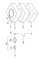
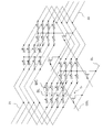
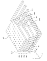
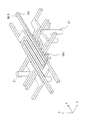
- FIG. 1 is a perspective view illustrating an overall configuration example of a memory device 1 according to the first embodiment of the present disclosure.
- FIG. 2 is an equivalent circuit diagram showing a part of the memory device 1 of FIG.
- the memory device 1 is a non-volatile storage device having a three-dimensional structure, and is formed on a semiconductor substrate 2 (hereinafter simply referred to as a substrate 2) having a main surface extending in the X-axis direction and the Y-axis direction in the Z-axis direction.
- a semiconductor substrate 2 hereinafter simply referred to as a substrate 2 having a main surface extending in the X-axis direction and the Y-axis direction in the Z-axis direction.
- Each of the n memory cell units MU includes one plate electrode WL, a plurality of columnar electrodes BL provided so as to intersect with each plate electrode WL, a plate electrode WL, and a plurality of columnar electrodes BL. And a plurality of memory cells MC respectively connected to both the plate-like electrode WL and the columnar electrode BL, and lead lines 4 that are connected to the plate-like electrode WL and form the connection portion 3. have.
- the plate-like electrode WL extends along the XY plane, and is provided in common to the plurality of columnar electrodes BL constituting each memory cell unit MU.
- the plurality of columnar electrodes BL are erected from the plate-shaped electrode WL toward the substrate 2.
- the columnar electrodes BL at positions overlapping each other in the Z-axis direction are connected through the plate-shaped electrode WL.
- the occupied area of the plate electrode WL (m + 1) in the (m + 1) th memory cell unit MU (m + 1) is larger than the occupied area of the plate electrode WLm in the mth memory cell unit MUm. Is also small. That is, the occupied area of the plate electrode WL2 in the memory cell unit MU2 is smaller than the occupied area of the plate electrode WL1 in the memory cell unit MU1.
- the occupied area of the plate electrode WL3 in the memory cell unit MU3 is smaller than the occupied area of the plate electrode WL2 in the memory cell unit MU2.
- the occupied area of the plate electrode WL3 in the memory cell unit MU3 is smaller than the occupied area of the plate electrode WL2 in the memory cell unit MU2.
- the occupied area of the plate electrode WL4 in the memory cell unit MU4 is smaller than the occupied area of the plate electrode WL3 in the memory cell unit MU3.
- FIG. 3 shows an enlarged perspective view (right side in the figure) showing an example of the configuration of the selection transistor Tr, and an equivalent circuit diagram (left side in the figure) corresponding thereto.
- the memory cell unit MU1 below the memory cell unit MU1, there are provided a plurality of gate selection lines GSL extending in the X-axis direction and arranged in the Y-axis direction.
- a plurality of source lines SL extending in the Y-axis direction and arranged in the X-axis direction are provided below the plurality of gate selection lines GSL.
- a contact line CL that connects the gate selection line GSL and the source line SL is provided at each intersection of the plurality of gate selection lines GSL and the plurality of source lines SL.
- the columnar electrode BL1 of the lowermost memory cell unit MU1 passes through the gate selection line GSL and is connected to the contact line CL.
- the columnar electrode BL1 and the gate selection line GSL are electrically insulated from each other by an insulating layer Z1 provided therebetween.
- the constituent material of the source line SL for example, a metal containing Cu, Al, W or the like is preferable.
- a conductive material containing one or more elements of C, Si, Ge, In, and Ga for example, carbon nanotubes or activated polysilicon
- other various wirings and various electrodes such as the gate selection line GSL, the plate-like electrode WL, and the columnar electrode BL may be configured using the same material as the constituent material of the source line SL unless otherwise specified. it can.
- each of the plurality of memory cell units MU has a memory cell region MR (MR1 to MR4) and a peripheral region PR (PR1 to PR4).
- the memory cell region MR is a region occupied by a plurality of memory cells MC. More specifically, among all the memory cells MC included in each memory cell unit MU, an area surrounded by a virtual line that sequentially connects several memory cells MC located on the outermost side in the XY plane (FIG. 1). The area surrounded by a broken line in FIG.
- the peripheral region PR refers to the remaining region excluding the memory cell region MR among the regions occupied by the plate-like electrodes WL constituting each memory cell unit MU.
- FIG. 4A shows an enlarged perspective view (right side in the figure) showing an example of the configuration of the memory cell MC in an enlarged manner and an equivalent circuit diagram (left side in the figure) corresponding thereto.
- FIG. 4A representatively shows the vicinity of an arbitrary memory cell MC in the first memory cell unit MU1.
- the columnar electrode BL1 of the lowermost memory cell unit MU1 penetrates the plate electrode WL1 in the Z-axis direction.
- the other memory cell units MU2 to MU4 have the same configuration.
- each memory cell MC mounted on the memory device 1 may have a selection element SEL inserted between the columnar electrode BL1 and the resistance change element VR.
- an access voltage is applied between the source line SL and the plate electrode WL, and the voltage of the gate selection line GSL is controlled to access the resistance change element VR.
- a pulse can be applied to change its resistance state or read its resistance state.
- a non-selected resistance change element VR is erroneously accessed by flowing a current to the resistance change element VR only when an access pulse larger than a certain voltage is applied. Has a role to prevent.
- the resistance change element VR has, for example, a stacked structure of an ion supply layer and an insulating layer.
- the material of the ion supply layer include a metal film containing one or more metal elements selected from Cu, Ag, Zr, and Al, an alloy film (for example, a CuTe alloy film), a metal compound film, and the like.
- metal elements other than Cu, Ag, Zr, and Al may be used as long as they have the property of being easily ionized.
- the element combined with at least one of Cu, Ag, Zr, and Al is preferably at least one element of S, Se, and Te.
- examples of the constituent material of the insulating layer in the resistance change element VR include SiN, SiO 2 , Gd 2 O 3, and the like.
- the size of the (m + 1) th memory cell region MR (m + 1) in the (m + 1) th memory cell unit MU (m + 1) is smaller than the size of the mth memory cell region MRm. It has become.
- the number of memory cells MC (the number of columnar electrodes BL (m + 1)) in the (m + 1) th memory cell unit MU (m + 1) is equal to the number of memory cells MC in the mth memory cell unit MUm. It is smaller than the number (the number of columnar electrodes BLm).
- a total of 80 memory cells MC and columnar electrodes BL1 (10 in the X direction and 8 in the Y direction) are arranged in the memory cell region MR1 in the memory cell unit MU1.
- a total of 70 (10 in the X direction and 7 in the Y direction) memory cells MC and columnar electrodes BL2 are arranged in the memory cell region MR2 of the memory cell unit MU2.
- a total of 60 (10 in the X direction and 6 in the Y direction) memory cells MC and columnar electrodes BL3 are arranged in the memory cell region MR3 of the memory cell unit MU3.
- a total of 50 (10 in the X direction and 5 in the Y direction) memory cells MC and columnar electrodes BL4 are arranged in the memory cell region MR4 of the memory cell unit MU4.
- the lead lines LL form a connection portion 3 with the first electrode WL, and contact pillars CP (CP1 to CP4) extending upward from the connection portion 3, that is, away from the substrate 2, It has a beam CB (CB1 to CB4) connected to the upper end of the contact pillar CP (CP1 to CP4) and extending in the XY plane (Y-axis direction in FIG. 1). The other end of the beam CB is connected to the drive circuit 4.
- the drive circuit 4 is embedded in, for example, the substrate 2 and executes a write operation to a desired memory cell MC and a read operation from the desired memory cell MC.
- the drive circuit 4 adjusts the voltage applied to the plate electrode WL, the columnar electrode BL, the gate selection line of the selection transistor Tr, and the like corresponding to the desired memory cell MC based on, for example, an external control signal.
- a plurality of lead lines LL (LL1 to LL4) may be provided for one plate electrode WL (WL1 to WL4).
- At least one connection unit 3 in the (m + 1) th memory cell unit MU (m + 1) is the mth memory cell MC surrounded by the plurality of memory cells MC in the mth memory cell unit MUm in the peripheral region PR (m + 1).
- the memory cell region MRm overlaps with the Z-axis direction. That is, the connection part 3 in the memory cell unit MU2 is in a position overlapping the memory cell region MR1 in the Z-axis direction in the peripheral region PR2.
- the connection portion 3 in the memory cell unit MU3 is in a position overlapping with the memory cell region MR2 in the Z-axis direction in the peripheral region PR3.
- connection part 3 in the memory cell unit MU4 is in a position overlapping with the memory cell region MR3 in the Z-axis direction in the peripheral region PR4.
- the connection part 3 in the (m + 1) th memory cell unit MU (m + 1) is at a position overlapping with any one of the plurality of memory cells MC in the mth memory cell unit MUm in the Z-axis direction. .
- the memory device 1 can be manufactured as follows, for example.
- FIG. 5A to 5E show a part of the manufacturing method of the memory device 1 in the order of steps.
- a substrate 2 having a main surface 2S along the XY plane is prepared, and a drive circuit 4 (not shown here) is formed on the main surface 2S.
- a plurality of source lines SL extending in the Y-axis direction are formed on the substrate 2 so as to be arranged in the X-axis direction.
- an insulating layer (not shown) made of SiO2 or the like is formed over the entire surface so as to cover the plurality of source lines SL, and then, as shown in FIG. 5B, X intersects with the plurality of source lines SL.
- a plurality of gate selection lines GSL extending in the axial direction and arranged in the Y-axis direction are formed. Further, at each intersection of the plurality of source lines SL and the plurality of gate selection lines GSL that overlap in the Z-axis direction, the gate selection line GSL and an insulating layer immediately below the gate selection line GSL are sandwiched between the source line SL and the gate selection line GSL. Through-holes K penetrating each other are formed.
- Each through hole reaches the upper surface of the source line SL.
- an insulating layer Z1 (see FIG. 3) is formed so as to cover the inner wall surfaces of the through holes K, and then the inside is filled with a predetermined conductive material, thereby forming the contact line CL.
- the plate-like electrode WL1 is formed so as to cover all the columnar electrodes BL1.
- the plate-like electrode WL1 has a size including the peripheral region PR1 around the memory cell region MR1 in which the plurality of memory cells MC are to be formed.
- through holes are provided at positions corresponding to the plurality of contact lines CL located below the plate-like electrode WL1.
- the variable resistance element VR is formed so as to cover the inner wall surfaces of the through holes, and the interior thereof is filled with a predetermined conductive material, so that a plurality of columnar electrodes BL1 are connected to the contact lines CL, respectively.
- Form see FIG. 4A.
- the plate electrode WL2 is formed above the plate electrode WL1.
- the dimension in the Y-axis direction of the plate electrode WL2 is made smaller than the dimension in the Y-axis direction of the plate electrode WL1 so as not to overlap with the peripheral region PR1.
- through-holes are respectively provided at positions corresponding to the plurality of columnar electrodes BL1 positioned below the plate-like electrode WL2.
- the resistance change element VR is formed so as to cover the inner wall surfaces of the through holes, and the interior thereof is filled with a predetermined conductive material, so that the columnar electrodes BL2 are connected to the respective columnar electrodes BL1.
- a plurality are formed.
- a memory cell unit MU2 in which a plurality of memory cells MC are arranged in the memory cell region MR2 is completed.
- the memory cell unit MU3 and the memory cell unit MU4 are formed in order as shown in FIG. 5E.
- the contact pillars CP1 to CP4 are collectively formed so as to stand in the peripheral regions PR1 to PR4 of the plate electrodes WL1 to WL4, respectively.
- the beams CB1 to CB4 are collectively formed so as to be connected to the upper ends of the contact pillars CP1 to CP4.
- the lead lines LL1 to LL4 are obtained.
- the memory device 1 is completed.
- connection portion 3 in the (m + 1) th memory cell unit MU (m + 1) is provided at a position overlapping the memory cell region MRm in the mth memory cell unit Mm in the Z-axis direction. That is, the memory cells MC constituting the memory cell unit MUm are also arranged below the peripheral region PR (m + 1) where the connection part 3 is provided in the memory cell unit MU (m + 1). Therefore, the memory device 1 as a whole can use the space efficiently and have more memory cells MC in the predetermined space. Therefore, high integration can be achieved.
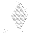
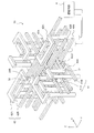
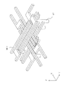
- FIG. 6 is a perspective view illustrating an overall configuration example of a memory device 1A that is a second modification of the memory device 1 described above.
- FIG. 7 is an equivalent circuit diagram showing a part of the memory device 1A of FIG.
- FIG. 8 shows an enlarged perspective view (right side in the figure) showing an enlarged configuration example of the memory cell MC and an equivalent circuit diagram (left side in the figure) corresponding thereto.
- the memory device 1B includes a first linear electrode 21 and a second line that extend in the Y-axis direction and are alternately arranged in the X-axis direction instead of the plate-like electrode WL.
- Each has a plurality of electrode 22.
- the columnar electrodes BL (BL1 to BL4) are sandwiched between the first linear electrode 21 and the second linear electrode 22 adjacent to each other in the X-axis direction in each of the memory cell units MU1 to MU4.
- the memory cell MC has resistances sandwiched between the columnar electrode BL and the first linear electrode 21 and between the columnar electrode BL and the second linear electrode 22, respectively.
- the change element VR is configured. In FIG. 6, the variable resistance element VR is not shown.
- lead lines 25 and 28 are provided as shown in FIG.
- the lead wire 25 is connected to the first linear electrode 21 to form the first connection portion 3A, and is connected to the upper end of the first contact pillar 23 and extends, for example, in the X-axis direction. And a first beam 24.
- the lead line 28 is connected to the second linear electrode 22 to form the second connection portion 3B, and is connected to the upper end of the second contact pillar 26 and extends, for example, in the X-axis direction.
- the second beam 27 is present.
- the plurality of first contact pillars 23 connected to the plurality of first linear electrodes 21 are connected in common to one first beam 24.
- a plurality of second contact pillars 26 connected to the plurality of second linear electrodes 22 are connected in common to one second beam 27, respectively. .
- This memory device 1B has a plurality of gate selection lines GSL arranged in the Y-axis direction and extending in the X-axis direction, and each of the plurality of gate selection lines GSL is arranged in the X-axis direction. Are connected to the columnar electrode BL.
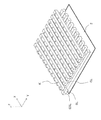
- FIG. 9 shows a main configuration of the memory device 1B in which the first beam 24 and the second beam 27 are omitted.
- the first linear electrode 21 and the second linear electrode 22 are arranged in a staircase pattern. That is, the dimension in the Y-axis direction of the first linear electrode 21 in the (m + 1) th memory cell unit MU (m + 1) is the same as that in the Y-axis direction of the first linear electrode 21 in the mth memory cell unit MUm. It is shorter than the dimensions. Similarly, the dimension in the Y-axis direction of the second linear electrode 22 in the memory cell unit MU (m + 1) is shorter than the dimension in the Y-axis direction of the second linear electrode 22 in the memory cell unit MUm.
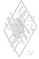
- FIG. 10 is a perspective view showing an overall configuration example of a memory device 1B which is a second modification of the memory device 1 described above.
- a through-hole is formed in the plate-like electrode WL to form the memory cell MC and the columnar electrode BL.
- a plurality of plate electrodes WL are stacked, and then a common through hole is formed for the plurality of plate electrodes WL. Also good.
- the formation of the memory cells MC and the columnar electrodes BL can be collectively formed over a plurality of memory cell units MU.
- FIG. 10 after laminating two plate electrodes WL, through holes are collectively formed in the two plate electrodes WL, and further, the memory cells MC and the columnar electrodes are filled so as to fill the through holes.
- BL is formed.
- a common through hole may be formed for three or more plate-like electrodes WL.
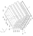
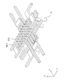
- FIG. 11 is a perspective view illustrating an overall configuration example of a memory device 1B according to the second embodiment of the present disclosure.
- FIG. 12 is an enlarged perspective view showing the vicinity of the memory cell MC applied to the memory device 1B shown in FIG. 11 and an equivalent circuit diagram thereof.
- FIG. 13 is a cross-sectional view schematically showing a cross-section of the main part of the memory device 1B.
- the memory device 1B includes a plurality of bit lines BL, a plurality of memory cells MC, and a plurality of word lines WL on the side of the substrate 2 (shown only in FIG. 13) in the Z-axis direction.
- the memory cell MC has a stacked structure in which a selection element SEL and a resistance change element VR are sequentially stacked from the substrate 2 side.
- the resistance change element VR has substantially the same planar shape as the word line WL or bit line BL immediately above it.
- the plurality of word lines WL are arranged so as to extend approximately in the X-axis direction and are aligned in the Y-axis direction, and the plurality of bit lines BL extend approximately in the Y-axis direction and are aligned in the X-axis direction. Is arranged.
- a plurality of selection elements SEL in the memory cell MC are arranged so as to be aligned in both the X-axis direction and the Y-axis direction.
- One resistance change element VR is provided in common to a plurality of selection elements SEL arranged in the X-axis direction, or is provided in common to a plurality of selection elements SEL arranged in the Y-axis direction.
- the (m + 1) th memory cell region MR (m + 1) surrounded by the plurality of memory cells MC in the (m + 1) th memory cell unit is narrower than the mth memory cell region MRm.
- a first contact pillar 31 that is connected to the word line WL as a lead line and forms a first connection portion 30A as a connection portion and extends away from the substrate 2, and a bit line BL that is connected to the bit line BL as a connection portion.
- the second contact pillar 32 is formed to form the second connection portion 30B and extend away from the substrate 2.
- the upper end of the first contact pillar 31 is connected to the drive circuit 4 by a wiring 41 including a beam 41A and a pillar 41B.
- the upper end of the second contact pillar 32 is connected to the drive circuit 4 by a wiring 42 including a beam 42A and a pillar 42B.
- This memory device 1B can be manufactured as follows, for example.
- FIG. 14A to 14L show a part of the manufacturing method of the memory device 1B in the order of steps.
- a substrate 2 having a main surface 2S along the XY plane is prepared, and a drive circuit 4 (not shown here) is formed on the main surface 2S.
- a plurality of contact lines CL are erected on the substrate 2, a plurality of bit lines BL0 extending in the Y-axis direction are arranged in the X-axis direction so as to be connected to the contact lines CL.
- a plurality of selection elements SEL are formed so as to form a matrix as a whole in the memory cell region MR (MR1).
- a plurality of selection elements SEL are erected on one bit line BL0 so as to be arranged at equal intervals in the Y-axis direction, for example.
- a region extending from the memory cell region MR to both sides along the Y-axis direction is referred to as a peripheral region (or contact region) PR (PR1).
- PR1 PR peripheral region PR
- a part of the bit line BL0 has a wide bent portion. This is because a contact line CL having a larger diameter than the width of the bit line BL0 can be arranged.
- the bit line BL0 is disconnected in FIGS.
- bit line BL0 in the two memory cell units is driven by one contact line CL.
- FIG. 14A eight bit lines BL0 are drawn, whereas the contact lines are arranged only on four bit lines BL0.
- the remaining four bit lines BL0 where the contact lines CL are not arranged are connected to and driven by the bit lines BL0 extending from the adjacent memory cell block MB.
- FIG. 14C After the resistance change element VR and the word line WL0 are sequentially stacked over the entire surface as the upper layer of the selection element SEL, a plurality of layers (FIG. 14C) extending approximately in the X-axis direction.
- patterning is performed so as to form a linear pattern of 8) as an example.
- the laminated pattern P0 having a laminated structure of the resistance change element VR and the word line WL0 extending in the X-axis direction is connected in common to the plurality of selection elements SEL arranged in the X-axis direction.
- the stacked structure of the resistance change element VR and the word line WL0 is drawn for only one of the 8 stacked patterns P0, but the structure is the same for the other stacked patterns P0.
- FIG. 14D shows an example in which four selection elements SEL are arranged on each stacked pattern P0.
- the memory cell region MR2 is narrower than the memory cell region MR1 (FIG. 14B).
- the resistance change element VR and the bit line BL1 are sequentially stacked over the entire surface as the upper layer of the selection element SEL, and then a plurality of them extending in the Y-axis direction (see FIG. 14E).
- patterning is performed so as to form a linear pattern of 4) as an example.
- the laminated pattern P1 that is a laminated structure of the resistance change element VR and the bit line BL1 extending in the Y-axis direction is connected in common to the plurality of selection elements SEL arranged in the Y-axis direction.
- the laminated structure of the resistance change element VR and the bit line BL1 is drawn for only one of the four laminated patterns P1, but the other laminated patterns P1 have the same structure.
- FIG. 14F shows an example in which four selection elements SEL are arranged on each stacked pattern P1.
- the memory cell region MR3 is narrower than the memory cell region MR2 (FIG. 14D).
- the resistance change element VR and the word line WL1 are sequentially stacked over the entire surface as the upper layer of the selection element SEL, a plurality of layers extending in the X-axis direction (see FIG. 14G).
- patterning is performed so as to form a linear pattern of 4) as an example.
- the stacked pattern P2 that is a stacked structure of the resistance change element VR extending in the X-axis direction and the word line WL1 is commonly connected to the plurality of selection elements SEL arranged in the X-axis direction.
- the laminated structure of the resistance change element VR and the word line WL1 is drawn for only one of the four laminated patterns P2, but the other laminated patterns P2 have the same structure.
- FIG. 14H shows an example in which four selection elements SEL are arranged on each stacked pattern P2.
- the memory cell region MR4 at this time is equivalent to the memory cell region MR3 (FIG. 14F).
- a variable resistance element VR and a bit line BL2 are sequentially stacked over the entire surface as an upper layer of the selection element SEL, and then a plurality of layers (FIG. 14J) extend approximately in the Y-axis direction.
- patterning is performed so as to form a linear pattern of 4) as an example.
- the stacked pattern P3 that is a stacked structure of the resistance change element VR extending in the X-axis direction and the bit line BL2 is connected in common to the plurality of selection elements SEL arranged in the Y-axis direction.
- the laminated structure of the resistance change element VR and the bit line BL2 is depicted for only one of the four laminated patterns P3, but the other laminated patterns P3 have the same structure.
- a plurality of first contact pillars 31 extending upward from the word lines WL and a plurality of second contact pillars 32 extending upward from the bit lines BL are formed.
- a plurality of pillars 41B and a plurality of pillars 42B connected to the drive circuit 4 are formed.
- the substrate 2 and the drive circuit 4 shown in FIG. 11 are omitted.
- a plurality of beams 41A are formed so as to connect the first contact pillar 31 and the pillar 41B, and the beam 42A is connected so as to connect the second contact pillar 32 and the pillar 42B.
- a plurality are formed.
- the substrate 2 and the drive circuit 4 shown in FIG. 11 are omitted.
- the memory device 1B is completed.
- the peripheral region PR and the memory cell region MR of a different hierarchy are configured to overlap each other, so that the space is efficiently used and more memory cells MC in the predetermined space. Can have. Therefore, high integration can be achieved.
- the resistance change element VR has substantially the same planar shape as the word line WL or the bit line BL immediately above the resistance change element VR, the manufacturing process can be simplified.
- FIG. 15 is a perspective view illustrating an overall configuration example of a memory device 1C according to the third embodiment of the present disclosure.
- FIG. 16 is an enlarged perspective view showing the vicinity of the memory cell MC applied to the memory device 1C shown in FIG. 15 and an equivalent circuit diagram thereof.
- the memory device 1B of the second embodiment four layers of memory cells MC are formed between the three layers of bit lines BL and the two layers of word lines WL.
- the three layers of the word line WL0, the bit line BL1, and the word line WL1 are connected to the two layers of memory cells MC.
- a leak current also flows through unselected memory cells MC.
- the memory cells MC, the bit lines BL, and the word lines WL have the same number of layers, and each bit line BL and the word line WL are connected only to one layer of memory cells MC. The structure is realized.
- the memory device 1C includes the word line WL0, the memory cell MC, the bit line BL0, the insulating layer, and the word line WL1 on the substrate 2 in the Z-axis direction.
- the memory cell MC and the bit line BL1 are sequentially stacked.
- the memory cell MC has a stacked structure in which a selection element SEL and a resistance change element VR are sequentially stacked from the substrate 2 side.
- the resistance change element VR has substantially the same planar shape as the bit line BL immediately above it.
- the memory device 1C includes a contact pillar 51 that is connected to the word line WL1 and extends downward (toward the substrate 2). Except for these points, the rest has substantially the same configuration as the memory device 1B of the second embodiment.
- the memory device 1C can be manufactured as follows, for example.
- 17A to 17G show a part of the manufacturing method of the memory device 1C in the order of steps.
- a plurality of contact lines CL are erected, a plurality of word lines WL0 extending in the Y-axis direction are connected in the X-axis direction so as to be connected to the contact lines CL.
- a plurality of selection elements SEL are formed so as to form a matrix as a whole in the memory cell region MR (MR1).
- MR memory cell region
- a plurality of (four in the example of FIG. 17B) selection elements SEL are erected on one bit line BL0 so as to be arranged at equal intervals in the Y-axis direction, for example.
- a region extending from the memory cell region MR to both sides along the Y-axis direction is referred to as a peripheral region (or contact region) PR (PR1).
- PR1 peripheral region PR
- a part of the word line WL0 has a wide bent portion. This is because a contact line CL having a larger diameter than the width of the word line WL0 can be arranged.
- the resistance change element VR and the bit line BL0 are sequentially stacked over the entire surface as the upper layer of the selection element SEL, and then a plurality of lines extending approximately in the X-axis direction. Batch patterning is performed to form a pattern.
- the resistance change element VR extending in the X-axis direction is commonly connected to a plurality of selection elements SEL arranged in the X-axis direction. Further, a contact pillar 51 for connecting to the word line WL1 to be formed later is formed.
- a plurality of word lines WL1 extending approximately in the Y-axis direction are formed.
- the word line WL1 is formed so as to be connected to the upper end of the contact pillar 51.
- a plurality of selection elements SEL are arranged in a matrix on each word line WL1.
- the resistance change element VR and the bit line BL1 are sequentially stacked over the entire surface as the upper layer of the selection element SEL, and then a plurality of lines extending approximately in the X-axis direction. Batch patterning is performed to form a pattern.
- the resistance change element VR extending in the X-axis direction is commonly connected to a plurality of selection elements SEL arranged in the X-axis direction.
- a plurality of pillars 53A and 53B connected to the drive circuit 4 are formed.
- a plurality of beams 54A are formed so as to connect the contact pillars 52A and the pillars 53A, and a plurality of beams 54B are formed so as to connect the contact pillars 52B and the pillars 53B.
- the memory device 1C is completed.
- FIGS. 18A and 18B show the peripheral region PR and the memory cell region MR of a different hierarchy overlap with each other, so that space is efficiently used. , It is possible to have more memory cells MC in a predetermined space. Therefore, high integration can be achieved.
- the resistance change element VR has substantially the same planar shape as the word line WL or the bit line BL immediately above the resistance change element VR, the manufacturing process can be simplified.
- 18A is a YZ cross section along the word line WL
- FIG. 18B is an XZ cross section along the bit line BL.
- each word line WL has a peripheral region PR at both ends in the Y-axis direction, and is connected to the drive circuit 4 (not shown) by contact pillars 51 extending downward. .
- the word line WL has an overhang structure in which the dimension of the word line WL in the Y-axis direction is increased toward the upper layer.
- the bit line BL has a staircase structure in which the dimension in the X-axis direction is reduced toward the upper layer. For this reason, the contact pillars 52 and the like for the respective bit lines BL can be formed collectively.
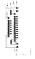
- FIG. 19 a memory including memory devices 1, 1A, 1B, and 1C (hereinafter collectively referred to as memory device 1) described in the first to third embodiments.
- the system will be described.
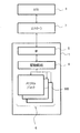
- the memory system shown in FIG. 19 includes a controller 7 and a host 8 in addition to the memory device 1.
- the controller 7 has a function for controlling the overall operation of the memory device 1 as a control unit.
- the host 8 is an external device that issues a command to the controller 7.
- the memory device 1 includes a memory cell block MB, a drive circuit 4, and an interface unit 5.
- the interface unit 5 has a data transmission / reception function with the controller 7.
- the memory cell block MB refers to one unit in which a plurality of memory cells MC shown in FIG. 1 and the like are integrated.
- a plurality of memory cell blocks MB are connected to one drive circuit 4.
- a plurality of memory cell blocks MB connected to one drive circuit 4 are collectively referred to as a memory cell block array 6.
- one columnar electrode BL that penetrates the memory cell units MU1 to MU4 in the Z-axis direction.
- Four memory cells are always arranged in (vertical wiring selected by GSL and SL).
- the region overlapping any of the peripheral regions (contact regions) PR1 to PR4 only 1 to 3 memory cells MC are arranged for one columnar electrode BL. Therefore, in an area overlapping any of the peripheral areas (contact areas) PR1 to PR4, an invalid address in which the memory cell MC does not exist is generated depending on the combination of the selection lines, and a discontinuous address area is generated in the physical address space.
- peripheral memory cells MC arranged in a region overlapping any of the peripheral regions PR (PR1 to PRn) are not used, and other memory cells MC are accessed for example.
- the controller 7 preferably has an address conversion table.
- the address conversion table is implemented as a function that returns an alternative address if substitution processing is performed, and returns 0 if substitution processing is not performed.
- the resistance change element VR when used as the memory cell MC, depending on the characteristics, it is necessary to perform an initialization process called forming before first writing after manufacturing. More specifically, as forming, (1) a high voltage is applied, (2) a long period of time is applied, and (3) a plurality of pulses are continuously applied, rather than a pulse applied to the memory cell MC in a normal writing process. One or more processes of applying are performed. It is desirable that the peripheral memory cells MC used for the above-described substitution processing are formed during substitution. This is because even if the memory cell used for the alternative processing is not directly accessed, the leakage current also flows into the memory cell by selecting the plate electrode WL or the columnar electrode BL for accessing another memory cell. This is because there is a possibility that the characteristics as a memory cell deteriorate. A memory cell that has not been formed (the state in which no forming has been performed after manufacturing) is preferable because this deterioration is smaller than that of a formed memory cell.
- a plurality of memory cells MC formed in a normal thin film process tend to exhibit stable characteristics when formed at positions other than the center of the other than those at both ends in a certain direction. From this point, in this memory system, a more stable operation can be expected by using the other memory cells MC without using the peripheral memory cells MC during normal operation.
- the configuration of the memory device 1 and the memory system has been specifically described in the above embodiment, but it is not necessary to include all the components, and other components may be further included.
- a resistance change element (resistance change memory) is used as a memory cell.
- the present technology is not limited to this, and for example, a phase change memory (PCM), an MRAM, Other types of memory such as STTRAM can be used.
- n memory cell units are sequentially stacked from the first to the nth in the first direction, The n memory cell units are respectively One or more first electrodes; A plurality of second electrodes provided so as to cross the first electrodes, A plurality of memory cells provided at respective intersections of the first electrode and the plurality of second electrodes, respectively connected to both the first electrode and the second electrode; One or more lead lines connected to the first electrode to form one or more connection portions; At least one of the connection portions in the (m + 1) th (m is a natural number equal to or less than n) memory cell unit is the mth memory cell region surrounded by the plurality of memory cells in the mth memory cell unit.
- a memory device in an overlapping position in the first direction (2) The memory device according to (1), wherein the connection portion in the (m + 1) th memory cell unit is in a position overlapping with the plurality of memory cells in the mth memory cell unit in the first direction. (3) The (m + 1) th memory cell region surrounded by the plurality of memory cells in the (m + 1) th memory cell unit is narrower than the mth memory cell region. (1) or (2) Memory devices. (4) The number of the plurality of memory cells in the (m + 1) th memory cell unit is smaller than the number of the plurality of memory cells in the mth memory cell unit. Any one of (1) to (3) The memory device according to one.
- the memory cell includes a resistance change element having a laminated structure of an ion supply layer and an insulating layer, The memory device according to any one of (1) to (4), wherein the variable resistance element is sandwiched between the first electrode and the second electrode. (6) The memory device according to any one of (1) to (5), further including a drive circuit connected to the lead line.
- the memory device As the first electrode, a plate-like electrode extending along a first surface orthogonal to the first direction, As the plurality of second electrodes, there are a plurality of columnar electrodes respectively erected from the plate electrode toward the substrate, The area occupied by the plate-like electrode in the (m + 1) th memory cell unit is smaller than the area occupied by the plate-like electrode in the m-th memory cell unit.
- First lines extending in a second direction along a first surface orthogonal to the first direction and alternately arranged in a third direction along the first surface as the first electrode
- As the plurality of second electrodes a plurality of columnar electrodes sandwiched between the adjacent first linear electrodes and the second linear electrodes, respectively,
- the plurality of memory cells are sandwiched between the plurality of columnar electrodes and the plurality of first linear electrodes and the plurality of second linear electrodes, respectively, facing each other across the plurality of columnar electrodes.
- a first contact pillar that is connected to the first linear electrode to form a first connection portion as the connection portion, and a second contact pole that is connected to the second linear electrode as the connection portion.
- the memory device according to any one of (1) to (6), further including a second contact pillar that forms a connection portion.
- the dimension of the first linear electrode in the (m + 1) th memory cell unit in the second direction is the dimension of the first linear electrode in the mth memory cell unit in the second direction. Shorter than The dimension of the second linear electrode in the (m + 1) th memory cell unit in the second direction is the dimension of the second linear electrode in the mth memory cell unit in the second direction.
- the memory device wherein the memory device is shorter.
- the plurality of first contact pillars connected to the plurality of first linear electrodes in the mth memory cell unit are commonly connected to one first beam,
- the plurality of second contact pillars connected to the plurality of second linear electrodes in the m-th memory cell unit are connected in common to one second beam (8) or
- the memory device according to 9 (1) A plurality of selection lines arranged in a second direction along the first surface and extending in a third direction intersecting the second direction along the first surface;
- the memory device according to (7), wherein each of the plurality of selection lines is connected to the plurality of second electrodes arranged in the third direction.
- the plurality of second electrodes, the plurality of memory cells, and the plurality of first electrodes are sequentially stacked from the substrate side,
- Each of the plurality of memory cells has a stacked structure in which a resistance change element and a selection element are sequentially stacked on the plurality of second electrodes,
- the memory device according to any one of (1) to (6), wherein the variable resistance element has substantially the same planar shape as any one of the plurality of first electrodes.
- the plurality of first electrodes extend in a second direction along the first surface and are arranged in a third direction orthogonal to the second direction,
- the plurality of second electrodes extend in the third direction and are arranged in the second direction,
- a plurality of the selection elements are arranged so as to be aligned in both the second direction and the third direction,
- the (m + 1) th memory cell region surrounded by the plurality of memory cells in the (m + 1) th memory cell unit is narrower than the mth memory cell region,
- a first contact pillar connected to the first electrode to form a first connection portion as the connection portion and extending away from the substrate, and connected to the second electrode as the connection portion
- a drive circuit provided between the substrate and the first memory cell unit; A first wiring connecting the upper end of the first contact pillar and the drive circuit;
- a first contact pillar connected to the first electrode to form a first connection portion as the connection portion and extending away from the substrate, and connected to the second electrode as the connection portion
- the memory device according to (12) or (13) further including a second contact pillar that forms a second connection portion of the first contact pillar and extends toward the substrate.
- a drive circuit provided between the substrate and the first memory cell unit; A first wiring connecting the upper end of the first contact pillar and the drive circuit; The memory device according to (16), further including: a second wiring that connects a lower end of the second contact pillar and the drive circuit.
- a memory device A control unit for controlling the memory device, The memory device is On the substrate, n memory cell units are sequentially stacked from the first to the nth in the first direction, The n memory cell units are respectively One or more first electrodes; A plurality of second electrodes provided so as to cross the first electrodes, A plurality of memory cells provided at respective intersections of the first electrode and the plurality of second electrodes, respectively connected to both the first electrode and the second electrode; One or more lead lines connected to the first electrode to form one or more connection portions; At least one of the connection portions in the (m + 1) th (m is a natural number equal to or less than n) memory cell unit is the mth memory cell region surrounded by the plurality of memory cells in the mth memory cell unit.
Landscapes
- Semiconductor Memories (AREA)
- Mram Or Spin Memory Techniques (AREA)
- Physics & Mathematics (AREA)
- Geometry (AREA)
Abstract
Description
1.第1の実施の形態(複数のWLが階段状に配置されたメモリデバイス)
2.変形例1(第1の実施の形態の第1の変形例)
3.変形例2(第1の実施の形態の第2の変形例)
4.第2の実施の形態(WLと実質的に同一の平面形状を有する抵抗変化素子を備えたメモリデバイス)
5.第3の実施の形態(WLと実質的に同一の平面形状を有する抵抗変化素子を備えた他のメモリデバイス)
6.適用例(メモリデバイスを備えたメモリシステム)
[メモリデバイス1の構成]
図1は、本開示の第1の実施の形態としてのメモリデバイス1の全体構成例を表す斜視図である。また、図2は、図1のメモリデバイス1の一部を表す等価回路図である。
このメモリデバイス1は、例えば次のようにして製造することができる。
メモリデバイス1では、第(m+1)番目のメモリセルユニットMU(m+1)における接続部3は、第m番目のメモリセルユニットMmにおけるメモリセル領域MRmとZ軸方向において重なり合う位置に設けられている。すなわち、メモリセルユニットMU(m+1)において接続部3が設けられた周辺領域PR(m+1)の下方にも、メモリセルユニットMUmを構成するメモリセルMCを配置するようにしている。このため、メモリデバイス1全体として、空間を効率的に利用し、所定の空間内においてより多くのメモリセルMCを有することができる。よって、高集積化を図ることができる。
図6は、上記したメモリデバイス1の第2の変形例であるメモリデバイス1Aの全体構成例を表した斜視図である。また、図7は、図6のメモリデバイス1Aの一部を表す等価回路図である。さらに、図8は、メモリセルMCの一構成例を拡大して表す拡大斜視図(図中右側)と、それに対応する等価回路図(図中左側)とを示したものである。
図10は、上記したメモリデバイス1の第2の変形例であるメモリデバイス1Bの全体構成例を表した斜視図である。上記第1の実施の形態のメモリデバイス1では、板状電極WLを1層積層するたびに、その板状電極WLに貫通孔を開け、メモリセルMCおよび柱状電極BLの形成を行うようにした。これに対し、本変形例のように、より製造工程を簡略化するために、複数の板状電極WLを積層したのち、複数の板状電極WLに対する共通の貫通孔の形成を行うようにしてもよい。その場合、メモリセルMCおよび柱状電極BLの形成を、複数のメモリセルユニットMUに亘って一括形成することができる。図10では、2つの板状電極WLを積層したのち、それら2つの板状電極WLに対して一括して貫通孔の形成を行い、さらに、その貫通孔を埋めるようにメモリセルMCおよび柱状電極BLの形成を行うようにしたものである。なお、3層以上の板状電極WLに対して共通の貫通孔の形成を行うようにしてもよい。
[メモリデバイス1Bの構成]
図11は、本開示の第2の実施の形態としてのメモリデバイス1Bの全体構成例を表す斜視図である。図12は、図11に示したメモリデバイス1Bに適用されるメモリセルMCの近傍を拡大して表す拡大斜視図およびその等価回路図である。また、図13は、メモリデバイス1Bの要部断面を概略的に表す断面図である。
このメモリデバイス1Bは、例えば次のようにして製造することができる。
メモリデバイス1Bにおいても、周辺領域PRと、それと異なる階層のメモリセル領域MRとが重複するように構成されているので、空間を効率的に利用し、所定の空間内においてより多くのメモリセルMCを有することができる。よって、高集積化を図ることができる。また、抵抗変化素子VRは、その直上のワード線WLもしくはビット線BLと実質的に同じ平面形状を有するので、製造工程の簡略化を図ることができる。
[メモリデバイス1Cの構成]
図15は、本開示の第3の実施の形態としてのメモリデバイス1Cの全体構成例を表す斜視図である。図16は、図15に示したメモリデバイス1Cに適用されるメモリセルMCの近傍を拡大して表す拡大斜視図およびその等価回路図である。上記第2の実施の形態のメモリデバイス1Bでは、3層のビット線BLと2層のワード線WLとの間に、4層のメモリセルMCが形成されるようにした。このような構成の場合、ワード線WL0、ビット線BL1およびワード線WL1の3つの層は、2層のメモリセルMCに接続される。クロスポイントメモリにおいては、選択されないメモリセルMCにもリーク電流が流れるので、メモリセルMCの層数が増加すると、駆動回路4に加わる負荷が大きくなるおそれがある。そこで、本実施の形態のメモリデバイス1Cでは、メモリセルMC、ビット線BLおよびワード線WLを同層数有するようにし、各ビット線BLおよびワード線WLは1層のメモリセルMCにのみ接続する構造を実現している。
このメモリデバイス1Cは、例えば次のようにして製造することができる。
メモリデバイス1Bにおいても、例えば図18Aおよび図18Bに示したように、周辺領域PRと、それと異なる階層のメモリセル領域MRとが重複するように構成されているので、空間を効率的に利用し、所定の空間内においてより多くのメモリセルMCを有することができる。よって、高集積化を図ることができる。また、抵抗変化素子VRは、その直上のワード線WLもしくはビット線BLと実質的に同じ平面形状を有するので、製造工程の簡略化を図ることができる。なお、図18Aは、ワード線WLに沿ったYZ断面であり、図18Bは、ビット線BLに沿ったXZ断面である。
次に、図19を参照して、上記第1から第3の実施の形態で説明したメモリデバイス1,1A,1B,1C(以下、ここではまとめてメモリデバイス1と記載する)を備えたメモリシステムについて説明する。図19に示したメモリシステムは、メモリデバイス1のほか、コントローラ7とホスト8とを備える。コントローラ7は、制御部としてメモリデバイス1の動作の全般を司る機能を有するものである。ホスト8は、コントローラ7に対して指令を出す外部装置である。
領域として認識させることができ、容易に扱うことができる。
(1)
基板の上に、第1の方向において第1番目から第n番目まで順に積層されたn個のメモ
リセルユニットを備え、
前記n個のメモリセルユニットは、それぞれ、
1以上の第1電極と、
前記第1電極と各々交差するように設けられた複数の第2電極と、
前記第1電極と前記複数の第2電極との各々の交差点に設けられ、前記第1電極と前記第2電極との双方にそれぞれ接続された複数のメモリセルと、
前記第1電極に接続されて1以上の接続部を形成する1以上の引き出し線と
を有し、
第(m+1)番目(mはn以下の自然数)の前記メモリセルユニットにおける少なくとも1つの前記接続部は、第m番目の前記メモリセルユニットにおいて前記複数のメモリセルが取り囲む第m番目のメモリセル領域と前記第1の方向において重なり合う位置にある
メモリデバイス。
(2)
前記第(m+1)番目のメモリセルユニットにおける前記接続部は、前記第m番目のメモリセルユニットにおける前記複数のメモリセルと前記第1の方向において重なり合う位置にある
上記(1)記載のメモリデバイス。
(3)
前記第(m+1)番目のメモリセルユニットにおいて前記複数のメモリセルが取り囲む第(m+1)番目のメモリセル領域は、前記第m番目のメモリセル領域よりも狭い
上記(1)または(2)に記載のメモリデバイス。
(4)
前記第(m+1)番目のメモリセルユニットにおける前記複数のメモリセルの数は、前記第m番目のメモリセルユニットにおける前記複数のメモリセルの数よりも少ない
上記(1)から(3)のいずれか1つに記載のメモリデバイス。
(5)
前記メモリセルは、イオン供給層と絶縁層との積層構造からなる抵抗変化素子を含み、
前記抵抗変化素子は、前記第1電極と前記第2電極との間に挟まれている
上記(1)から(4)のいずれか1つに記載のメモリデバイス。
(6)
前記引き出し線と接続された駆動回路をさらに有する
上記(1)から(5)のいずれか1つに記載のメモリデバイス。
(7)
前記第1電極として、前記第1の方向と直交する第1の面に沿って広がる板状電極を有し、
前記複数の第2電極として、前記板状電極から前記基板へ向けてそれぞれ立設された複数の柱状電極を有し、
前記第(m+1)番目のメモリセルユニットにおける前記板状電極の占有面積は、前記第m番目のメモリセルユニットにおける前記板状電極の占有面積よりも小さい
上記(1)から(6)のいずれか1つに記載のメモリデバイス。
(8)
前記第1電極として、前記第1の方向と直交する第1の面に沿った第2の方向にそれぞれ延在すると共に前記第1の面に沿った第3の方向において交互に並ぶ第1線状電極と第2線状電極とをそれぞれ複数有し、
前記複数の第2電極として、隣り合う前記第1線状電極と前記第2線状電極との間にそれぞれ挟まれた複数の柱状電極を有し、
前記複数のメモリセルとして、前記複数の柱状電極と、前記複数の柱状電極をそれぞれ挟んで対向する前記複数の第1線状電極および前記複数の第2線状電極との間にそれぞれ挟まれた複数の記憶層を有し、
前記引き出し線として、前記第1線状電極と接続されて前記接続部としての第1接続部分を形成する第1コンタクトピラーと、前記第2線状電極と接続されて前記接続部としての第2接続部分を形成する第2コンタクトピラーとを有する
上記(1)から(6)のいずれか1つに記載のメモリデバイス。
(9)
前記第(m+1)番目のメモリセルユニットにおける前記第1線状電極の前記第2の方向の寸法は、前記第m番目のメモリセルユニットにおける前記第1線状電極の前記第2の方向の寸法よりも短く、
前記第(m+1)番目のメモリセルユニットにおける前記第2線状電極の前記第2の方向の寸法は、前記第m番目のメモリセルユニットにおける前記第2線状電極の前記第2の方向の寸法よりも短い
上記(8)記載のメモリデバイス。
(10)
前記第m番目のメモリセルユニットにおける複数の前記第1線状電極と接続された複数の前記第1コンタクトピラーは、一の第1ビームに対して共通に接続されており、
前記第m番目のメモリセルユニットにおける複数の前記第2線状電極と接続された複数の前記第2コンタクトピラーは、一の第2ビームに対して共通に接続されている
上記(8)または(9)に記載のメモリデバイス。
(11)
前記第1の面に沿った第2の方向に並び、かつ、前記第1の面に沿って前記第2の方向と交差する第3の方向に延在する複数の選択線を有し、
前記複数の選択線の各々は、前記第3の方向に並ぶ前記複数の第2電極と接続されている
上記(7)記載のメモリデバイス。
(12)
前記第1の方向において、前記複数の第2電極と前記複数のメモリセルと複数の前記第1電極とが前記基板の側から順に積層され、
前記複数のメモリセルは、それぞれ、前記複数の第2電極の上に抵抗変化素子と選択素子とが順に積層された積層構造を有し、
前記抵抗変化素子は、前記複数の第1電極のうちのいずれか1つと実質的に同じ平面形状を有する
上記(1)から(6)のいずれか1つに記載のメモリデバイス。
(13)
前記複数の第1電極は、前記第1の面に沿った第2の方向へそれぞれ延在すると共に前記第2の方向と直交する第3の方向に並ぶように配置され、
前記複数の第2電極は、前記第3の方向へそれぞれ延在すると共に前記第2の方向に並ぶように配置され、
前記選択素子は、前記第2の方向および前記第3の方向の双方において並ぶように複数配置され、
前記第2の方向または前記第3の方向に並ぶ複数の前記選択素子に対し、1つの前記抵抗変化素子が共通に接続されている
上記(12)記載のメモリデバイス。
(14)
前記第(m+1)番目のメモリセルユニットにおいて前記複数のメモリセルが取り囲む第(m+1)番目のメモリセル領域は、前記第m番目のメモリセル領域よりも狭く、
前記引き出し線として、前記第1電極と接続されて前記接続部としての第1接続部分を形成し前記基板から遠ざかるように伸びる第1コンタクトピラーと、前記第2電極と接続されて前記接続部としての第2接続部分を形成し前記基板から遠ざかるように伸びる第2コンタクトピラーとを有する
上記(12)または(13)に記載のメモリデバイス。
(15)
前記基板と第1番目の前記メモリセルユニットとの間に設けられた駆動回路と、
前記第1コンタクトピラーの上端と前記駆動回路とを接続する第1配線と、
前記第2コンタクトピラーの上端と前記駆動回路とを接続する第2配線と
をさらに有する
上記(14)記載のメモリデバイス。
(16)
前記引き出し線として、前記第1電極と接続されて前記接続部としての第1接続部分を
形成し前記基板から遠ざかるように伸びる第1コンタクトピラーと、前記第2電極と接続されて前記接続部としての第2接続部分を形成し前記基板へ向かうように伸びる第2コンタクトピラーとを有する
上記(12)または(13)に記載のメモリデバイス。
(17)
前記基板と第1番目の前記メモリセルユニットとの間に設けられた駆動回路と、
前記第1コンタクトピラーの上端と前記駆動回路とを接続する第1配線と、
前記第2コンタクトピラーの下端と前記駆動回路とを接続する第2配線と
をさらに有する
上記(16)記載のメモリデバイス。
(18)
メモリデバイスと、
前記メモリデバイスの制御を行う制御部と
を備え、
前記メモリデバイスは、
基板の上に、第1の方向において第1番目から第n番目まで順に積層されたn個のメモリセルユニットを備え、
前記n個のメモリセルユニットは、それぞれ、
1以上の第1電極と、
前記第1電極と各々交差するように設けられた複数の第2電極と、
前記第1電極と前記複数の第2電極との各々の交差点に設けられ、前記第1電極と前記第2電極との双方にそれぞれ接続された複数のメモリセルと、
前記第1電極に接続されて1以上の接続部を形成する1以上の引き出し線と
を有し、
第(m+1)番目(mはn以下の自然数)の前記メモリセルユニットにおける少なくとも1つの前記接続部は、第m番目の前記メモリセルユニットにおいて前記複数のメモリセルが取り囲む第m番目のメモリセル領域と前記第1の方向において重なり合う位置にある
メモリシステム。
(19)
前記第m番目のメモリセル領域のうち、前記第(m+1)番目のメモリセルユニットにおいて前記複数のメモリセルが取り囲む第(m+1)番目のメモリセル領域と前記第1の方向において重なり合う領域以外の周辺領域に設けられた前記メモリセルが、予備メモリセルとして機能する
上記(18)記載のメモリシステム。
Claims (19)
- 基板の上に、第1の方向において第1番目から第n番目まで順に積層されたn個のメモリセルユニットを備え、
前記n個のメモリセルユニットは、それぞれ、
1以上の第1電極と、
前記第1電極と各々交差するように設けられた複数の第2電極と、
前記第1電極と前記複数の第2電極との各々の交差点に設けられ、前記第1電極と前記第2電極との双方にそれぞれ接続された複数のメモリセルと、
前記第1電極に接続されて1以上の接続部を形成する1以上の引き出し線と
を有し、
第(m+1)番目(mはn以下の自然数)の前記メモリセルユニットにおける少なくとも1つの前記接続部は、第m番目の前記メモリセルユニットにおいて前記複数のメモリセルが取り囲む第m番目のメモリセル領域と前記第1の方向において重なり合う位置にある
メモリデバイス。 - 前記第(m+1)番目のメモリセルユニットにおける前記接続部は、前記第m番目のメモリセルユニットにおける前記複数のメモリセルと前記第1の方向において重なり合う位置にある
請求項1記載のメモリデバイス。 - 前記第(m+1)番目のメモリセルユニットにおいて前記複数のメモリセルが取り囲む第(m+1)番目のメモリセル領域は、前記第m番目のメモリセル領域よりも狭い
請求項1記載のメモリデバイス。 - 前記第(m+1)番目のメモリセルユニットにおける前記複数のメモリセルの数は、前記第m番目のメモリセルユニットにおける前記複数のメモリセルの数よりも少ない
請求項1記載のメモリデバイス。 - 前記メモリセルは、イオン供給層と絶縁層との積層構造からなる抵抗変化素子を含み、
前記抵抗変化素子は、前記第1電極と前記第2電極との間に挟まれている
請求項1記載のメモリデバイス。 - 前記引き出し線と接続された駆動回路をさらに有する
請求項1記載のメモリデバイス。 - 前記第1電極として、前記第1の方向と直交する第1の面に沿って広がる板状電極を有し、
前記複数の第2電極として、前記板状電極から前記基板へ向けてそれぞれ立設された複数の柱状電極を有し、
前記第(m+1)番目のメモリセルユニットにおける前記板状電極の占有面積は、前記第m番目のメモリセルユニットにおける前記板状電極の占有面積よりも小さい
請求項1記載のメモリデバイス。 - 前記第1電極として、前記第1の方向と直交する第1の面に沿った第2の方向にそれぞれ延在すると共に前記第1の面に沿った第3の方向において交互に並ぶ第1線状電極と第2線状電極とをそれぞれ複数有し、
前記複数の第2電極として、隣り合う前記第1線状電極と前記第2線状電極との間にそれぞれ挟まれた複数の柱状電極を有し、
前記複数のメモリセルとして、前記複数の柱状電極と、前記複数の柱状電極をそれぞれ挟んで対向する前記複数の第1線状電極および前記複数の第2線状電極との間にそれぞれ挟まれた複数の記憶層を有し、
前記引き出し線として、前記第1線状電極と接続されて前記接続部としての第1接続部分を形成する第1コンタクトピラーと、前記第2線状電極と接続されて前記接続部としての第2接続部分を形成する第2コンタクトピラーとを有する
請求項1記載のメモリデバイス。 - 前記第(m+1)番目のメモリセルユニットにおける前記第1線状電極の前記第2の方向の寸法は、前記第m番目のメモリセルユニットにおける前記第1線状電極の前記第2の方向の寸法よりも短く、
前記第(m+1)番目のメモリセルユニットにおける前記第2線状電極の前記第2の方向の寸法は、前記第m番目のメモリセルユニットにおける前記第2線状電極の前記第2の方向の寸法よりも短い
請求項8記載のメモリデバイス。 - 前記第m番目のメモリセルユニットにおける複数の前記第1線状電極と接続された複数の前記第1コンタクトピラーは、一の第1ビームに対して共通に接続されており、
前記第m番目のメモリセルユニットにおける複数の前記第2線状電極と接続された複数の前記第2コンタクトピラーは、一の第2ビームに対して共通に接続されている
請求項8記載のメモリデバイス。 - 前記第1の面に沿った第2の方向に並び、かつ、前記第1の面に沿って前記第2の方向と交差する第3の方向に延在する複数の選択線を有し、
前記複数の選択線の各々は、前記第3の方向に並ぶ前記複数の第2電極と接続されている
請求項7記載のメモリデバイス。 - 前記第1の方向において、前記複数の第2電極と前記複数のメモリセルと複数の前記第1電極とが前記基板の側から順に積層され、
前記複数のメモリセルは、それぞれ、前記複数の第2電極の上に抵抗変化素子と選択素子とが順に積層された積層構造を有し、
前記抵抗変化素子は、前記複数の第1電極のうちのいずれか1つと実質的に同じ平面形状を有する
請求項1記載のメモリデバイス。 - 前記複数の第1電極は、前記第1の面に沿った第2の方向へそれぞれ延在すると共に前記第2の方向と直交する第3の方向に並ぶように配置され、
前記複数の第2電極は、前記第3の方向へそれぞれ延在すると共に前記第2の方向に並ぶように配置され、
前記選択素子は、前記第2の方向および前記第3の方向の双方において並ぶように複数配置され、
前記第2の方向または前記第3の方向に並ぶ複数の前記選択素子に対し、1つの前記抵抗変化素子が共通に接続されている
請求項12記載のメモリデバイス。 - 前記第(m+1)番目のメモリセルユニットにおいて前記複数のメモリセルが取り囲む第(m+1)番目のメモリセル領域は、前記第m番目のメモリセル領域よりも狭く、
前記引き出し線として、前記第1電極と接続されて前記接続部としての第1接続部分を形成し前記基板から遠ざかるように伸びる第1コンタクトピラーと、前記第2電極と接続されて前記接続部としての第2接続部分を形成し前記基板から遠ざかるように伸びる第2コンタクトピラーとを有する
請求項12記載のメモリデバイス。 - 前記基板と第1番目の前記メモリセルユニットとの間に設けられた駆動回路と、
前記第1コンタクトピラーの上端と前記駆動回路とを接続する第1配線と、
前記第2コンタクトピラーの上端と前記駆動回路とを接続する第2配線と
をさらに有する
請求項14記載のメモリデバイス。 - 前記引き出し線として、前記第1電極と接続されて前記接続部としての第1接続部分を形成し前記基板から遠ざかるように伸びる第1コンタクトピラーと、前記第2電極と接続されて前記接続部としての第2接続部分を形成し前記基板へ向かうように伸びる第2コンタクトピラーとを有する
請求項12記載のメモリデバイス。 - 前記基板と第1番目の前記メモリセルユニットとの間に設けられた駆動回路と、
前記第1コンタクトピラーの上端と前記駆動回路とを接続する第1配線と、
前記第2コンタクトピラーの下端と前記駆動回路とを接続する第2配線と
をさらに有する
請求項16記載のメモリデバイス。 - メモリデバイスと、
前記メモリデバイスの制御を行う制御部と
を備え、
前記メモリデバイスは、
基板の上に、第1の方向において第1番目から第n番目まで順に積層されたn個のメモリセルユニットを備え、
前記n個のメモリセルユニットは、それぞれ、
1以上の第1電極と、
前記第1電極と各々交差するように設けられた複数の第2電極と、
前記第1電極と前記複数の第2電極との各々の交差点に設けられ、前記第1電極と前記第2電極との双方にそれぞれ接続された複数のメモリセルと、
前記第1電極に接続されて1以上の接続部を形成する1以上の引き出し線と
を有し、
第(m+1)番目(mはn以下の自然数)の前記メモリセルユニットにおける少なくとも1つの前記接続部は、第m番目の前記メモリセルユニットにおいて前記複数のメモリセルが取り囲む第m番目のメモリセル領域と前記第1の方向において重なり合う位置にある
メモリシステム。 - 前記第m番目のメモリセル領域のうち、前記第(m+1)番目のメモリセルユニットにおいて前記複数のメモリセルが取り囲む第(m+1)番目のメモリセル領域と前記第1の方向において重なり合う領域以外の周辺領域に設けられた前記メモリセルが、予備メモリセルとして機能する
請求項18記載のメモリシステム。
Priority Applications (6)
| Application Number | Priority Date | Filing Date | Title |
|---|---|---|---|
| KR1020177034368A KR20180016365A (ko) | 2015-06-10 | 2016-05-18 | 메모리 디바이스 및 메모리 시스템 |
| DE112016002610.2T DE112016002610T5 (de) | 2015-06-10 | 2016-05-18 | Speichervorrichtung und Speichersystem |
| CN201680032405.0A CN107615482B (zh) | 2015-06-10 | 2016-05-18 | 存储设备和存储系统 |
| US15/579,302 US10319787B2 (en) | 2015-06-10 | 2016-05-18 | Memory device and memory system |
| US16/402,838 US10700130B2 (en) | 2015-06-10 | 2019-05-03 | Memory device and memory system |
| US15/930,297 US11049905B2 (en) | 2015-06-10 | 2020-05-12 | Memory device and memory system |
Applications Claiming Priority (2)
| Application Number | Priority Date | Filing Date | Title |
|---|---|---|---|
| JP2015-117228 | 2015-06-10 | ||
| JP2015117228A JP2017005097A (ja) | 2015-06-10 | 2015-06-10 | メモリデバイスおよびメモリシステム |
Related Child Applications (2)
| Application Number | Title | Priority Date | Filing Date |
|---|---|---|---|
| US15/579,302 A-371-Of-International US10319787B2 (en) | 2015-06-10 | 2016-05-18 | Memory device and memory system |
| US16/402,838 Continuation US10700130B2 (en) | 2015-06-10 | 2019-05-03 | Memory device and memory system |
Publications (1)
| Publication Number | Publication Date |
|---|---|
| WO2016199556A1 true WO2016199556A1 (ja) | 2016-12-15 |
Family
ID=57503897
Family Applications (1)
| Application Number | Title | Priority Date | Filing Date |
|---|---|---|---|
| PCT/JP2016/064772 Ceased WO2016199556A1 (ja) | 2015-06-10 | 2016-05-18 | メモリデバイスおよびメモリシステム |
Country Status (7)
| Country | Link |
|---|---|
| US (3) | US10319787B2 (ja) |
| JP (1) | JP2017005097A (ja) |
| KR (1) | KR20180016365A (ja) |
| CN (1) | CN107615482B (ja) |
| DE (1) | DE112016002610T5 (ja) |
| TW (1) | TWI713196B (ja) |
| WO (1) | WO2016199556A1 (ja) |
Families Citing this family (10)
| Publication number | Priority date | Publication date | Assignee | Title |
|---|---|---|---|---|
| US9553132B1 (en) * | 2015-09-09 | 2017-01-24 | Kabushiki Kaisha Toshiba | Semiconductor memory device |
| US10249639B2 (en) * | 2016-02-01 | 2019-04-02 | Toshiba Memory Corporation | Semiconductor memory device |
| JP2018200967A (ja) * | 2017-05-29 | 2018-12-20 | ソニーセミコンダクタソリューションズ株式会社 | 半導体装置 |
| JP2021027205A (ja) * | 2019-08-06 | 2021-02-22 | キオクシア株式会社 | 半導体記憶装置及びその製造方法 |
| KR102743836B1 (ko) * | 2020-01-08 | 2024-12-16 | 삼성전자주식회사 | 반도체 메모리 장치 및 그 제조 방법 |
| JP2021150493A (ja) | 2020-03-19 | 2021-09-27 | キオクシア株式会社 | 半導体記憶装置 |
| US11805636B2 (en) | 2020-06-18 | 2023-10-31 | Taiwan Semiconductor Manufacturing Co., Ltd. | Memory device |
| US11404113B2 (en) * | 2020-06-18 | 2022-08-02 | Taiwan Semiconductor Manufacturing Co., Ltd. | Memory device including a word line with portions with different sizes in different metal layers |
| JP2022076684A (ja) * | 2020-11-10 | 2022-05-20 | ソニーセミコンダクタソリューションズ株式会社 | 半導体装置 |
| TWI810036B (zh) * | 2022-05-26 | 2023-07-21 | 南亞科技股份有限公司 | 具有可編程部件的半導體元件 |
Citations (4)
| Publication number | Priority date | Publication date | Assignee | Title |
|---|---|---|---|---|
| JP2009170082A (ja) * | 2008-01-15 | 2009-07-30 | Samsung Electronics Co Ltd | 3次元アレイ構造を備えるメモリ装置及びそのリペア方法 |
| US20110316072A1 (en) * | 2010-06-24 | 2011-12-29 | Samsung Electronics Co., Ltd. | Semiconductor memory devices including asymmetric word line pads |
| WO2013076935A1 (ja) * | 2011-11-22 | 2013-05-30 | パナソニック株式会社 | 抵抗変化型不揮発性記憶装置、および抵抗変化型不揮発性記憶装置のアクセス方法 |
| WO2014103577A1 (ja) * | 2012-12-26 | 2014-07-03 | ソニー株式会社 | 記憶装置およびその製造方法 |
Family Cites Families (11)
| Publication number | Priority date | Publication date | Assignee | Title |
|---|---|---|---|---|
| US7948021B2 (en) * | 2007-04-27 | 2011-05-24 | Kabushiki Kaisha Toshiba | Semiconductor memory device and method of fabricating the same |
| KR101583717B1 (ko) * | 2009-01-13 | 2016-01-11 | 삼성전자주식회사 | 저항 메모리 장치의 제조방법 |
| JP2011114011A (ja) | 2009-11-24 | 2011-06-09 | Hitachi Ltd | 不揮発性記憶装置およびその製造方法 |
| KR20110111809A (ko) | 2010-04-05 | 2011-10-12 | 삼성전자주식회사 | 계단형 구조를 구현할 수 있는 패터닝 방법 및 이를 이용한 불휘발성 메모리 소자의 제조 방법 |
| KR101137770B1 (ko) * | 2010-09-09 | 2012-04-24 | 한국과학기술원 | 3차원 구조의 비휘발성 메모리 소자, 그 제조 방법 및 메모리 칩 |
| US8467229B2 (en) | 2010-11-24 | 2013-06-18 | Panasonic Corporation | Variable resistance nonvolatile memory device |
| KR20120094339A (ko) * | 2011-02-16 | 2012-08-24 | 에스케이하이닉스 주식회사 | 3차원 구조의 비휘발성 메모리 소자 및 그 제조 방법 |
| JP5765430B2 (ja) * | 2011-10-07 | 2015-08-19 | 株式会社日立製作所 | 半導体記憶装置及びその製造方法 |
| JP2013084715A (ja) * | 2011-10-07 | 2013-05-09 | Toshiba Corp | 不揮発性半導体記憶装置およびその製造方法 |
| US9076723B1 (en) * | 2014-03-10 | 2015-07-07 | Kabushiki Kaisha Toshiba | Non-volatile memory device and method for manufacturing same |
| KR102358302B1 (ko) * | 2015-05-21 | 2022-02-04 | 삼성전자주식회사 | 수직형 낸드 플래시 메모리 소자 및 그 제조 방법 |
-
2015
- 2015-06-10 JP JP2015117228A patent/JP2017005097A/ja active Pending
-
2016
- 2016-05-18 KR KR1020177034368A patent/KR20180016365A/ko not_active Withdrawn
- 2016-05-18 US US15/579,302 patent/US10319787B2/en active Active
- 2016-05-18 WO PCT/JP2016/064772 patent/WO2016199556A1/ja not_active Ceased
- 2016-05-18 CN CN201680032405.0A patent/CN107615482B/zh not_active Expired - Fee Related
- 2016-05-18 DE DE112016002610.2T patent/DE112016002610T5/de not_active Withdrawn
- 2016-05-26 TW TW105116460A patent/TWI713196B/zh not_active IP Right Cessation
-
2019
- 2019-05-03 US US16/402,838 patent/US10700130B2/en not_active Expired - Fee Related
-
2020
- 2020-05-12 US US15/930,297 patent/US11049905B2/en not_active Expired - Fee Related
Patent Citations (4)
| Publication number | Priority date | Publication date | Assignee | Title |
|---|---|---|---|---|
| JP2009170082A (ja) * | 2008-01-15 | 2009-07-30 | Samsung Electronics Co Ltd | 3次元アレイ構造を備えるメモリ装置及びそのリペア方法 |
| US20110316072A1 (en) * | 2010-06-24 | 2011-12-29 | Samsung Electronics Co., Ltd. | Semiconductor memory devices including asymmetric word line pads |
| WO2013076935A1 (ja) * | 2011-11-22 | 2013-05-30 | パナソニック株式会社 | 抵抗変化型不揮発性記憶装置、および抵抗変化型不揮発性記憶装置のアクセス方法 |
| WO2014103577A1 (ja) * | 2012-12-26 | 2014-07-03 | ソニー株式会社 | 記憶装置およびその製造方法 |
Also Published As
| Publication number | Publication date |
|---|---|
| JP2017005097A (ja) | 2017-01-05 |
| CN107615482A (zh) | 2018-01-19 |
| DE112016002610T5 (de) | 2018-03-01 |
| US10700130B2 (en) | 2020-06-30 |
| US20200273909A1 (en) | 2020-08-27 |
| CN107615482B (zh) | 2021-12-31 |
| TWI713196B (zh) | 2020-12-11 |
| US10319787B2 (en) | 2019-06-11 |
| US20180175108A1 (en) | 2018-06-21 |
| US11049905B2 (en) | 2021-06-29 |
| KR20180016365A (ko) | 2018-02-14 |
| US20190259811A1 (en) | 2019-08-22 |
| TW201711166A (zh) | 2017-03-16 |
Similar Documents
| Publication | Publication Date | Title |
|---|---|---|
| CN107615482B (zh) | 存储设备和存储系统 | |
| JP2021044397A (ja) | 半導体記憶装置 | |
| JP2020155543A (ja) | 半導体記憶装置 | |
| CN105556608B (zh) | 半导体存储装置 | |
| JP2019057532A (ja) | 半導体メモリ | |
| JP2020150199A (ja) | 半導体記憶装置 | |
| JP2019212687A (ja) | 半導体メモリ | |
| TW202127632A (zh) | 半導體記憶裝置 | |
| JP2021044446A (ja) | 半導体記憶装置及びその製造方法 | |
| TWI717794B (zh) | 半導體記憶體 | |
| JP2016167332A (ja) | 記憶装置 | |
| JP2012168999A (ja) | 不揮発性半導体記憶装置の動作方法 | |
| JP2021019083A (ja) | 半導体記憶装置 | |
| CN113345901A (zh) | 半导体存储装置 | |
| TWI692082B (zh) | 半導體記憶裝置 | |
| JP2016072534A (ja) | 記憶装置 | |
| JP2022061710A (ja) | 記憶装置 | |
| US11152037B2 (en) | Semiconductor memory device | |
| US12507416B2 (en) | Memory device including memory blocks different from each other | |
| KR20240025814A (ko) | 비휘발성 메모리 장치 및 이를 포함하는 메모리 패키지 | |
| TWI834083B (zh) | 記憶體元件 | |
| TW202232728A (zh) | 半導體記憶裝置 | |
| TWI836805B (zh) | 半導體記憶裝置 | |
| US20250311213A1 (en) | Memory device including dummy memory block | |
| JP2024018698A (ja) | 半導体記憶装置 |
Legal Events
| Date | Code | Title | Description |
|---|---|---|---|
| 121 | Ep: the epo has been informed by wipo that ep was designated in this application |
Ref document number: 16807263 Country of ref document: EP Kind code of ref document: A1 |
|
| ENP | Entry into the national phase |
Ref document number: 20177034368 Country of ref document: KR Kind code of ref document: A |
|
| WWE | Wipo information: entry into national phase |
Ref document number: 15579302 Country of ref document: US |
|
| WWE | Wipo information: entry into national phase |
Ref document number: 112016002610 Country of ref document: DE |
|
| 122 | Ep: pct application non-entry in european phase |
Ref document number: 16807263 Country of ref document: EP Kind code of ref document: A1 |