WO2016194369A1 - 半導体光変調素子 - Google Patents
半導体光変調素子 Download PDFInfo
- Publication number
- WO2016194369A1 WO2016194369A1 PCT/JP2016/002649 JP2016002649W WO2016194369A1 WO 2016194369 A1 WO2016194369 A1 WO 2016194369A1 JP 2016002649 W JP2016002649 W JP 2016002649W WO 2016194369 A1 WO2016194369 A1 WO 2016194369A1
- Authority
- WO
- WIPO (PCT)
- Prior art keywords
- layer
- type
- cladding layer
- semiconductor
- type cladding
- Prior art date
Links
Images


Classifications
-
- G—PHYSICS
- G02—OPTICS
- G02F—OPTICAL DEVICES OR ARRANGEMENTS FOR THE CONTROL OF LIGHT BY MODIFICATION OF THE OPTICAL PROPERTIES OF THE MEDIA OF THE ELEMENTS INVOLVED THEREIN; NON-LINEAR OPTICS; FREQUENCY-CHANGING OF LIGHT; OPTICAL LOGIC ELEMENTS; OPTICAL ANALOGUE/DIGITAL CONVERTERS
- G02F1/00—Devices or arrangements for the control of the intensity, colour, phase, polarisation or direction of light arriving from an independent light source, e.g. switching, gating or modulating; Non-linear optics
- G02F1/01—Devices or arrangements for the control of the intensity, colour, phase, polarisation or direction of light arriving from an independent light source, e.g. switching, gating or modulating; Non-linear optics for the control of the intensity, phase, polarisation or colour
- G02F1/21—Devices or arrangements for the control of the intensity, colour, phase, polarisation or direction of light arriving from an independent light source, e.g. switching, gating or modulating; Non-linear optics for the control of the intensity, phase, polarisation or colour by interference
- G02F1/225—Devices or arrangements for the control of the intensity, colour, phase, polarisation or direction of light arriving from an independent light source, e.g. switching, gating or modulating; Non-linear optics for the control of the intensity, phase, polarisation or colour by interference in an optical waveguide structure
- G02F1/2257—Devices or arrangements for the control of the intensity, colour, phase, polarisation or direction of light arriving from an independent light source, e.g. switching, gating or modulating; Non-linear optics for the control of the intensity, phase, polarisation or colour by interference in an optical waveguide structure the optical waveguides being made of semiconducting material
-
- G—PHYSICS
- G02—OPTICS
- G02F—OPTICAL DEVICES OR ARRANGEMENTS FOR THE CONTROL OF LIGHT BY MODIFICATION OF THE OPTICAL PROPERTIES OF THE MEDIA OF THE ELEMENTS INVOLVED THEREIN; NON-LINEAR OPTICS; FREQUENCY-CHANGING OF LIGHT; OPTICAL LOGIC ELEMENTS; OPTICAL ANALOGUE/DIGITAL CONVERTERS
- G02F1/00—Devices or arrangements for the control of the intensity, colour, phase, polarisation or direction of light arriving from an independent light source, e.g. switching, gating or modulating; Non-linear optics
- G02F1/01—Devices or arrangements for the control of the intensity, colour, phase, polarisation or direction of light arriving from an independent light source, e.g. switching, gating or modulating; Non-linear optics for the control of the intensity, phase, polarisation or colour
- G02F1/015—Devices or arrangements for the control of the intensity, colour, phase, polarisation or direction of light arriving from an independent light source, e.g. switching, gating or modulating; Non-linear optics for the control of the intensity, phase, polarisation or colour based on semiconductor elements with at least one potential jump barrier, e.g. PN, PIN junction
- G02F1/025—Devices or arrangements for the control of the intensity, colour, phase, polarisation or direction of light arriving from an independent light source, e.g. switching, gating or modulating; Non-linear optics for the control of the intensity, phase, polarisation or colour based on semiconductor elements with at least one potential jump barrier, e.g. PN, PIN junction in an optical waveguide structure
-
- G—PHYSICS
- G02—OPTICS
- G02F—OPTICAL DEVICES OR ARRANGEMENTS FOR THE CONTROL OF LIGHT BY MODIFICATION OF THE OPTICAL PROPERTIES OF THE MEDIA OF THE ELEMENTS INVOLVED THEREIN; NON-LINEAR OPTICS; FREQUENCY-CHANGING OF LIGHT; OPTICAL LOGIC ELEMENTS; OPTICAL ANALOGUE/DIGITAL CONVERTERS
- G02F1/00—Devices or arrangements for the control of the intensity, colour, phase, polarisation or direction of light arriving from an independent light source, e.g. switching, gating or modulating; Non-linear optics
- G02F1/01—Devices or arrangements for the control of the intensity, colour, phase, polarisation or direction of light arriving from an independent light source, e.g. switching, gating or modulating; Non-linear optics for the control of the intensity, phase, polarisation or colour
- G02F1/21—Devices or arrangements for the control of the intensity, colour, phase, polarisation or direction of light arriving from an independent light source, e.g. switching, gating or modulating; Non-linear optics for the control of the intensity, phase, polarisation or colour by interference
- G02F1/225—Devices or arrangements for the control of the intensity, colour, phase, polarisation or direction of light arriving from an independent light source, e.g. switching, gating or modulating; Non-linear optics for the control of the intensity, phase, polarisation or colour by interference in an optical waveguide structure
-
- G—PHYSICS
- G02—OPTICS
- G02F—OPTICAL DEVICES OR ARRANGEMENTS FOR THE CONTROL OF LIGHT BY MODIFICATION OF THE OPTICAL PROPERTIES OF THE MEDIA OF THE ELEMENTS INVOLVED THEREIN; NON-LINEAR OPTICS; FREQUENCY-CHANGING OF LIGHT; OPTICAL LOGIC ELEMENTS; OPTICAL ANALOGUE/DIGITAL CONVERTERS
- G02F1/00—Devices or arrangements for the control of the intensity, colour, phase, polarisation or direction of light arriving from an independent light source, e.g. switching, gating or modulating; Non-linear optics
- G02F1/01—Devices or arrangements for the control of the intensity, colour, phase, polarisation or direction of light arriving from an independent light source, e.g. switching, gating or modulating; Non-linear optics for the control of the intensity, phase, polarisation or colour
- G02F1/21—Devices or arrangements for the control of the intensity, colour, phase, polarisation or direction of light arriving from an independent light source, e.g. switching, gating or modulating; Non-linear optics for the control of the intensity, phase, polarisation or colour by interference
- G02F1/212—Mach-Zehnder type
-
- G—PHYSICS
- G02—OPTICS
- G02F—OPTICAL DEVICES OR ARRANGEMENTS FOR THE CONTROL OF LIGHT BY MODIFICATION OF THE OPTICAL PROPERTIES OF THE MEDIA OF THE ELEMENTS INVOLVED THEREIN; NON-LINEAR OPTICS; FREQUENCY-CHANGING OF LIGHT; OPTICAL LOGIC ELEMENTS; OPTICAL ANALOGUE/DIGITAL CONVERTERS
- G02F2202/00—Materials and properties
- G02F2202/10—Materials and properties semiconductor
- G02F2202/102—In×P and alloy
-
- G—PHYSICS
- G02—OPTICS
- G02F—OPTICAL DEVICES OR ARRANGEMENTS FOR THE CONTROL OF LIGHT BY MODIFICATION OF THE OPTICAL PROPERTIES OF THE MEDIA OF THE ELEMENTS INVOLVED THEREIN; NON-LINEAR OPTICS; FREQUENCY-CHANGING OF LIGHT; OPTICAL LOGIC ELEMENTS; OPTICAL ANALOGUE/DIGITAL CONVERTERS
- G02F2202/00—Materials and properties
- G02F2202/10—Materials and properties semiconductor
- G02F2202/107—Zn×S or Zn×Se and alloys
Definitions
- the present invention relates to a semiconductor optical modulation element that functions as a high-speed optical modulator in the field of optical communication.
- MZ optical modulators are listed as important element devices that control their characteristics, and many researches and developments have been made. Particularly in recent years, in order to realize further miniaturization and low power consumption, attention has been focused on optical modulators made of compound semiconductor materials such as InP as well as optical modulators made of lithium niobate (LN).
- the compound semiconductor optical modulator In order to operate as an optical modulator, an interaction between electricity (electric field) and propagating light is used. Generally, a core layer that confines light is a non-doped layer, and the layer is sandwiched between p-type and n-type clad layers in order from the upper layer, and a reverse bias voltage is applied to realize a strong interaction between light and electricity.
- a core layer that confines light is a non-doped layer, and the layer is sandwiched between p-type and n-type clad layers in order from the upper layer, and a reverse bias voltage is applied to realize a strong interaction between light and electricity.
- the p-type semiconductor used here has a material electrical resistivity and optical absorptance higher by an order of magnitude or more than those of an n-type semiconductor, it has major problems in speeding up the modulation operation and reducing optical loss. Yes.
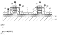
- FIG. 1 As an approach by improving the semiconductor layer, a semiconductor light modulator having a cross-sectional structure as shown in FIG. 1 has been proposed in the past (for example, Patent Documents 1 and 2).
- the semiconductor light modulation device shown in FIG. 1 has a high mesa waveguide structure laminated on a substrate 10.
- a high-mesa waveguide is used, but a semiconductor MZ modulator is generally a general configuration in order to enhance the interaction of the photoelectric device and reduce the parasitic capacitance.
- the signal electrode 16 is provided on the waveguide structure via the n-type contact layer 15.
- the ground electrode 17 is provided on the n-type cladding layer 11.
- FIG. 1 shows an npin-type optical modulator in which the upper and lower cladding layers 11 and 14 of the non-doped layer 12 are n-type, and a thin p-type layer is inserted as a carrier block layer 13 for suppressing electron current between both n layers. Since this npin type does not use a p-type cladding having a large optical loss, a relatively long waveguide can be used. In addition, since there is a degree of freedom that the thickness of the depletion layer can be arbitrarily designed optimally, it is easy to satisfy the drive voltage reduction and electrical speed / light speed matching at the same time, which is advantageous for increasing the response speed of the modulator. .
- FIG. 2 shows the RF band characteristics in the npin layer structure calculated by the calculation simulation.
- the main cause of the surge resistance variation is that the function of the p-type semiconductor as a carrier block layer is lowered due to damage to the waveguide sidewall caused by dry etching.
- the instability of the modulation operation has problems such as the dependency of the modulation efficiency on the incident light power, the dependency of the modulation efficiency on the bias voltage, and the reduction of the breakdown voltage. It is considered that this is mainly because hole carriers are concentrated in the p layer of the high mesa waveguide.
- Non-patent Document 1 discloses a pin structure from the viewpoint of electrical stability
- an electroabsorption (EA) modulator in which the upper clad is n-type, the lower clad, and the substrate is p-type (nip structure) is also proposed (patent document 5) with the aim of reducing contact resistance.
- EA electroabsorption
- the electrode structure of the EA modulator is generally a lumped constant type, it is not necessary to satisfy the characteristic impedance and the speed matching condition between the light wave and the microwave.
- an MZ modulator whose electrode length is approximately an order of magnitude longer than that of an EA modulator, it is not sufficient to improve the modulation band simply by inverting only the semiconductor layer structure. This is also clear from the fact that, when comparing pin and nip in FIG.
- Patent Document 4 when a conductive substrate (P-type substrate) is used, the parasitic capacitance is larger than that of a semi-insulating substrate. The problem remains in diverting as it is.
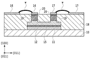
- Non-Patent Document 1 As an approach by improving the electrode structure, a cross-sectional structure as shown in FIG. 3 has been proposed (for example, Non-Patent Document 1). 3 adopts a capacitively loaded electrode structure in which a coplanar strip line having an electrode having a large cross-sectional area is used as a main line, and a lumped constant electrode (capacitance) divided by a length sufficiently shorter than a microwave is added on an optical waveguide. Yes. A signal electrode 16 and a ground electrode 17 are provided on the p-type cladding layer 19 via a p-type contact layer 20. As a result, high speed can be expected by reducing the loss of the main line, and the characteristic impedance and the speed matching condition can be controlled independently, so that the degree of freedom in design is very high.
- JP 2008-233710 A Japanese Patent Laying-Open No. 2005-099387 JP 2005-114868 A JP 2008-107468 A JP-A-8-122719
- the electrode structure shown in FIG. 3 is only applied to the semiconductor element having a pin structure from the upper layer, and the ultimate high-speed modulation operation has not been achieved by optimizing both the semiconductor layer and the electrode structure.
- a dry etching process must be used to etch the upper cladding layer vertically as shown in FIG.
- the number indicated by an asterisk (*) in the crystal plane notation means “1 is overlined”. This is because the wet etching process has a so-called forward mesa orientation, so that the processed shape becomes a trapezoidal shape, resulting in deterioration of electrical characteristics. Therefore, the controllability of the etching depth cannot be ensured, and there is a possibility that optical characteristics are deteriorated and an electrically unstable operation is caused by interface damage during processing.
- the problem to the electric surge and unstable operation remains, and the conventional p-type optical modulation element having a high contact resistance and material resistance has a high p-layer resistance.
- the mold cladding layer has been required to have an adverse effect on high speed and high processing accuracy when processing the ridge waveguide.
- the present invention has been made in view of the above-described conventional problems, and an object of the present invention is to provide a Mach-Zehnder type (MZ) semiconductor optical modulation element that can be used as a modulator that is ultrafast and excellent in electrical stability. There is.
- MZ Mach-Zehnder type
- the invention described in one embodiment is an input / output device that performs multiplexing / demultiplexing of a refractive index modulation region that modulates the refractive index of light to be guided and light branched in the refractive index modulation region.
- a Mach-Zehnder type semiconductor light modulation device that modulates light with an output region, wherein the optical waveguide is equivalent to the (100) plane of a zinc blende semi-insulating semiconductor crystal substrate in the refractive index modulation region.
- a p-type cladding layer, an i-core layer, and an n-type cladding layer are laminated on a smooth substrate surface, and the n-type cladding layer and the InP cladding layer are formed in a ridge shape in the reverse mesa direction, and the refractive index modulation region
- a semiconductor light modulation device comprising a capacitor-loaded electrode on the n-type cladding layer.
- FIG. 6 is a diagram illustrating a refractive index modulation region of a semiconductor light modulation element according to Example 2.
- FIG. 6 is a diagram showing a cross section of an input / output region of a semiconductor light modulation device of Example 2.
- FIG. 6 is a diagram showing a cross section of an input / output region of a semiconductor light modulation device of Example 2.
- FIG. 4 is a plan view of the semiconductor light modulation device of the present invention
- FIG. 5 is a cross-sectional view of the refractive index modulation region (VV ′) of the semiconductor light modulation device
- FIG. It is sectional drawing of the input-output area
- the refractive index modulation region refers to a region that modulates the refractive index of the core layer by applying an electric signal to cause a secondary optical effect in the core layer.
- the semiconductor optical modulation device of the present invention is configured as a Mach-Zehnder type optical waveguide L having a capacitance loaded traveling wave electrode pattern P formed on the upper surface.
- the optical waveguide modulates light by a refractive index modulation region that modulates the refractive index of the guided light and an input / output region that performs multiplexing / demultiplexing of the light branched in the refractive index modulation region.
- An n-type cladding layer 14, an i-core layer 12, and a p-type cladding layer 19 are laminated.
- the n-type cladding layer 14 is formed in a ridge shape in the reverse mesa direction, and a capacitive load is formed on the n-type cladding layer 14. It has a configuration in which electrodes are provided.
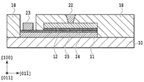
- the optical waveguide is formed from the upper layer on the substrate surface equivalent to the (100) plane of the zincblende semi-insulating semiconductor crystal substrate 10 in a portion where the refractive index of light is not modulated.
- a semi-insulating InP cladding layer 22, an i-core layer 12, and a p-type cladding layer 19 are laminated.
- the zinc blende type semi-insulating semiconductor crystal substrate 10 for example, an InP substrate can be used.
- an n-type cladding layer 14, an i-core layer 12, and a p-type cladding layer (p-type carrier stop layer) are formed on the substrate surface equivalent to the (100) plane of the zincblende semi-insulating semiconductor crystal substrate 10.
- ) 19 are sequentially stacked, and the n-type cladding layer 14 that does not modulate the refractive index of light is removed and backfilled with a semi-insulating InP cladding layer 22, and then the [011] plane direction with respect to the cladding layer
- the Mach-Zehnder type waveguide shape By etching the Mach-Zehnder type waveguide shape in the direction equivalent to, the cladding layer of the light modulation waveguide can be formed in a ridge shape in the reverse mesa direction.
- a capacitively loaded electrode structure can be formed on the upper surface of the n-type cladding layer 14.
- Etching the Mach-Zehnder waveguide shape in the direction equivalent to the [011] plane direction on the cladding layers 14 and 22 forms the claddings 14 and 22 of the light modulation waveguide in a ridge shape in the reverse mesa direction. .
- the signal electrode 16 and the ground electrode 17 are formed on the upper surface of the n-type cladding layer 14 via the n-type contact layer 15, and the signal electrode 16 provided on the insulating films on both sides of the waveguide. Alternatively, it is electrically connected to the ground electrode 17 with a bonding wire w.
- the capacitively loaded electrode can be connected to a differential signal source via a differential line wiring board.
- the p-type cladding layer 19 is in contact with an electrode 23 connected to a power source through a p-type contact layer 21.
- the semiconductor optical modulation elements shown in FIGS. 4, 5, and 6 modulate the refractive index by generating a secondary electro-optic effect in the i core layer 12 and modulate the light guided through the Mach-Zehnder type optical waveguide. ing.
- the waveguide mesa upper portion (the upper layer of the core) having a small contact area with the electrode in order to realize the contact resistance reduction which has been a problem in the conventional capacitively loaded electrode modulator.
- the contact resistance is reduced by about one digit compared to the conventional case.
- the waveguide stripe direction (waveguide longitudinal direction) is set to a direction equivalent to the [011] ridge direction, and the insulating film is etched in the reverse mesa direction.
- the thickness of the p-type cladding layer which has a larger bulk material resistance than that of the n-type, is reduced, and the upper and lower sides of the core layer and the thin film p-layer are sandwiched between the n-type cladding layers, resulting in the ultimate reduction in semiconductor resistance A simple modulator.
- an electrode is brought into contact with a p-type semiconductor in which hole carriers are accumulated, and the accumulated carriers are extracted.
- a ridge structure waveguide is used in the modulation region while ensuring high-speed operation by reducing contact resistance and reducing the thickness of the p-type cladding layer (reducing resistance), thereby providing electrical surge resistance.
- a semiconductor optical device used as a high-speed modulator can be manufactured.
- holes accumulated in the p-type layer diffuse to the slab waveguide side outside the light propagation region, so that the hole concentration per unit volume can be reduced as compared with the high mesa waveguide structure. Further, a further decrease in hole concentration can be expected by making these p-type layers conductive with electrodes connected to a power source. As a result, unstable modulation operation is suppressed.
- a p-type layer is deposited below the non-doped layer (nip, nipn structure), and these devices are etched in a direction equivalent to the [011] plane direction to fill the n-type cladding layer, thereby providing light modulation guidance.
- Example 1 an optical semiconductor element having the cross section shown in FIGS.
- the semiconductor light modulation device of this example has a nip type configuration.
- the semiconductor layers are stacked on the substrate 10 in the order of the n-type contact layer 15, the n-type cladding layer 14, the non-doped cladding / core layer 12, the p-type cladding 19, and the p-type contact layer 21.
- the upper n-type contact layer 15 is made of InGaAs with a carrier concentration of 5E + 18 cm ⁇ 3
- the n-type cladding layer 14 is made of InP with a carrier concentration of 1E + 18 cm ⁇ 3
- the carrier concentration of the p-type InP clad layer 19 was set to 5E + 17 to 1E + 18 cm ⁇ 3 in view of the light absorption coefficient and the electrical resistivity.
- the p-type contact layer 21 was made of InGaAs doped with hole carriers at 5E + 18 cm ⁇ 3 or more in order to reduce contact resistance.
- An InGaAsP layer 15 was inserted into the uppermost layer of the non-doped layer 12 in order to utilize the selectivity with the n-type cladding layer 14 of InP in wet etching.
- the band gap wavelength of the core layer 12 is determined in such a range that the electro-optic effect is effectively applied with high efficiency at the operating light wavelength and the light absorption does not become a problem.
- the emission wavelength of the core layer 12 is set to about 1.4 microns.
- the core layer 12 is preferably formed of an InGaAlAs / InAlAs multiple quantum well structure from the viewpoint of high-efficiency modulation, but the usefulness of the present invention is not lost even if it is formed as a multiple structure such as InGaAsP / InP, InGaAsP / InGaAsP, for example. Is clear. Further, the compositions of the contact layers 15 and 21 and the cladding layers 14 and 19 are not limited to the above, and there is no problem if an InGaAsP composition is used, for example.
- the upper n-type cladding layer 14 in a region where the refractive index of light is not modulated is removed by dry etching and wet etching for the purpose of electrical isolation between elements. Further, from the viewpoint of reducing optical loss, the removed portion is further backfilled with semi-insulating InP22.
- an MZ interferometer waveguide pattern made of SiO 2 formed in a direction equivalent to the [011] plane direction is formed, and a ridge-shaped optical waveguide is formed in the reverse mesa direction using dry etching and wet etching. .
- the n-type contact layer 15 and a part of the n-type cladding layer 14 are dry-etched, the n-type cladding layer 14 is wet-etched to form a ridge-shaped optical waveguide in the reverse mesa direction.
- dry / wet etching is further performed to expose a part of the p-type contact layer 21 and contact with the electrode 23 as shown in FIG.
- BCB ⁇ ⁇ ⁇ Benzocyclobutene
- a predetermined bias is applied to the DC bias electrode 23 so that a reverse electric field is applied to the pn junction, and then a high frequency signal is applied to the signal electrode (coplanar strip). Power to the track).
- a predetermined bias is applied to the DC bias electrode 23 so that a reverse electric field is applied to the pn junction, and then a high frequency signal is applied to the signal electrode (coplanar strip). Power to the track).
- it can be driven by feeding a single-phase signal, but it has been found that there is no problem if the modulator is driven by feeding a differential signal from the viewpoint of reducing power consumption.
- Example 2 7 and 8 are views showing a cross section of a semiconductor light modulation device according to Example 2 of the present invention.
- 7 is a cross-sectional view taken along the line VV ′ of FIG. 4
- FIG. 6 is a cross-sectional view taken along the line VI-VI ′ of FIG.
- the semiconductor light modulation device of this example has a nipn configuration.
- the semiconductor optical modulation element includes an n-type contact layer 15, an n-type cladding layer 14, an undoped cladding / core layer 12, a p-type carrier block layer (25, an n-type contact 24, an n-type cladding layer 11 from the upper layer.
- the layers are sequentially stacked on the substrate 10.
- the carrier concentration of the upper n-type contact layer 15 is 5E + 18 cm ⁇ 3 InGaAs
- the carrier concentration of the n-type cladding layer 14 is 1E + 18 cm ⁇ 3 InP.
- the p-type carrier block layer 25 was doped with 1E + 18 cm ⁇ 3 hole carriers in InAlAs having a large band gap so as to provide a sufficient barrier against electrons. Note that an InGaAsP layer 15 was inserted into the uppermost layer of the non-doped layer in order to utilize the selectivity with the n-type cladding layer 14 of InP in wet etching.
- the band gap wavelength of the core layer 12 is determined in such a range that the electro-optic effect is effectively applied with high efficiency at the operating light wavelength and the light absorption does not become a problem.
- the emission wavelength of the core layer 12 is set to about 1.4 microns.
- the core layer 12 is preferably formed of an InGaAlAs / InAlAs multiple quantum well structure from the viewpoint of high-efficiency modulation, but the usefulness of the present invention is not lost even if it is formed as a multiple structure such as InGaAsP / InP, InGaAsP / InGaAsP, for example. Is clear.
- the composition of the contact / cladding / carrier blocking layer 13 is not limited to the above, and for example, an InGaAsP composition may be used.
- the upper n-type cladding layer 14 in a region where the refractive index of light is not modulated is removed by dry etching and wet etching for the purpose of electrical isolation between elements. Further, from the viewpoint of reducing optical loss, the removed portion is further backfilled with semi-insulating InP22.
- an MZ interferometer waveguide pattern made of SiO 2 formed in a direction equivalent to the [011] plane direction is formed, and a ridge-shaped optical waveguide is formed using dry etching and wet etching.
- BCB Benzocyclobutene
- a capacitively loaded traveling wave electrode pattern P as shown in FIG. 4 is formed by a gold plating method.
- polyimide or the like which is an insulating low refractive index material, is used.
- a predetermined bias is applied to the DC bias electrode 23 so that a reverse electric field is applied to the pn junction, and then a high frequency signal is applied to the signal electrode (coplanar strip). Power to the track).
- a predetermined bias is applied to the DC bias electrode 23 so that a reverse electric field is applied to the pn junction, and then a high frequency signal is applied to the signal electrode (coplanar strip). Power to the track).
- it can be driven by feeding a single-phase signal, but it has been found that there is no problem if the modulator is driven by feeding a differential signal from the viewpoint of reducing power consumption.
Abstract
Description
実施例1では、図5、6に示す断面を有する光半導体素子を作製した。本実施例の半導体光変調素子は、nip型の構成を有する。半導体層は上層からn型コンタクト層15、n型クラッド層14、ノンドープクラッド・コア層12、p型クラッド19、p型コンタクト層21の順に基板10上に積層されている。
図7、8は本発明の実施例2に係る半導体光変調素子の断面を示す図である。図7は図4のV-V’断面図であり、図6は図4のVI-VI’断面図である。本実施例の半導体光変調素子は、nipn型の構成を有する。同図において、半導体光変調素子は、上層からn型コンタクト層15、n型クラッド層14、ノンドープクラッド・コア層12、p型キャリアブロック層(25、n型コンタクト24、n型クラッド層11の順に基板10上に積層されている。
11 n型クラッド層
12 iコア層
13 p型キャリアブロック層
14 n型クラッド層
15 n型コンタクト層
16 信号電極
17 接地電極
18 絶縁膜
19 p型クラッド層
20 p型コンタクト層
21 p型コンタクト層
22 SI型クラッド層
23 DCバイアス電極
24 n型コンタクト層
25 p型キャリアブロック層
L 光導波路
P 進行波電極パターン
w ボンディングワイヤ
Claims (6)
- 光導波路に導波する光の屈折率を変調する屈折率変調領域と該屈折率変調領域で分岐する光の合分波を行う入出力領域とによって光の変調を行うマッハツェンダ型の半導体光変調素子であって、
前記光導波路は、屈折率変調領域においては、閃亜鉛鉱形半絶縁性の半導体結晶基板の(100)面と等価な基板面上に、上層から基板面に向かって少なくともn型クラッド層とiコア層とp型クラッド層とが積層されており、前記n型クラッド層は逆メサ方向にリッジ形状に形成され、該n型クラッド層上に容量装荷電極を設けたことを特徴とする半導体光変調素子。 - 前記光導波路は、光の屈折率を変調しない部分においては、閃亜鉛鉱形半絶縁性の半導体結晶基板の(100)面と等価な基板面上に、上層から基板面に向かって少なくとも半絶縁性のInPクラッド層とiコア層とp型クラッド層とが積層されていることを特徴とする請求項1に記載の半導体光変調素子。
- 前記n型クラッド層は、[011]面方向と等価な方向にマッハツェンダ型導波路形状にエッチングが施されることによって、逆メサ方向にリッジ形状となるように形成されることを特徴とする請求項1または2に記載の半導体光変調素子。
- 前記光導波路が上層から基板面に向かって順に少なくともn型クラッド層、iコア層、p型クラッド層、n型クラッド層を含む半導体多層構造から構成されることを特徴とする請求項1から3のいずれかに記載の半導体光変調素子。
- 前記p型クラッド層と電源に接続された電極とを電気的に接触させていることを特徴とする請求項4に記載の半導体光変調素子。
- 前記容量装荷電極が差動線路配線板を介して差動信号源と接続されていることを特徴とする請求項1から5のいずれかに記載の半導体光変調素子。
Priority Applications (5)
| Application Number | Priority Date | Filing Date | Title |
|---|---|---|---|
| EP16802809.0A EP3306381B1 (en) | 2015-06-02 | 2016-06-01 | Semiconductor optical modulation element |
| CA2988051A CA2988051C (en) | 2015-06-02 | 2016-06-01 | Semiconductor optical modulation element |
| JP2017521693A JP6458143B2 (ja) | 2015-06-02 | 2016-06-01 | 半導体光変調素子 |
| US15/577,918 US10254624B2 (en) | 2015-06-02 | 2016-06-01 | Semiconductor optical modulation element |
| CN201680031603.5A CN107615140B (zh) | 2015-06-02 | 2016-06-01 | 半导体光调制元件 |
Applications Claiming Priority (2)
| Application Number | Priority Date | Filing Date | Title |
|---|---|---|---|
| JP2015-112448 | 2015-06-02 | ||
| JP2015112448 | 2015-06-02 |
Publications (1)
| Publication Number | Publication Date |
|---|---|
| WO2016194369A1 true WO2016194369A1 (ja) | 2016-12-08 |
Family
ID=57440465
Family Applications (1)
| Application Number | Title | Priority Date | Filing Date |
|---|---|---|---|
| PCT/JP2016/002649 WO2016194369A1 (ja) | 2015-06-02 | 2016-06-01 | 半導体光変調素子 |
Country Status (7)
| Country | Link |
|---|---|
| US (1) | US10254624B2 (ja) |
| EP (1) | EP3306381B1 (ja) |
| JP (1) | JP6458143B2 (ja) |
| CN (1) | CN107615140B (ja) |
| CA (1) | CA2988051C (ja) |
| TW (1) | TWI638464B (ja) |
| WO (1) | WO2016194369A1 (ja) |
Cited By (2)
| Publication number | Priority date | Publication date | Assignee | Title |
|---|---|---|---|---|
| WO2020149185A1 (ja) * | 2019-01-16 | 2020-07-23 | 日本電信電話株式会社 | 半導体マッハツェンダ光変調器 |
| WO2023095261A1 (ja) * | 2021-11-25 | 2023-06-01 | 三菱電機株式会社 | マッハツェンダ変調器 |
Families Citing this family (12)
| Publication number | Priority date | Publication date | Assignee | Title |
|---|---|---|---|---|
| US10534204B2 (en) | 2017-11-03 | 2020-01-14 | International Business Machines Corporation | Structured photorefractive layer stack |
| CN111373312B (zh) * | 2017-11-30 | 2023-08-04 | 三菱电机株式会社 | 半导体光调制器 |
| JP7247120B2 (ja) * | 2018-02-08 | 2023-03-28 | 古河電気工業株式会社 | 光集積素子および光モジュール |
| WO2019155679A1 (ja) * | 2018-02-09 | 2019-08-15 | 三菱電機株式会社 | 光半導体素子およびその製造方法 |
| WO2019159345A1 (ja) * | 2018-02-19 | 2019-08-22 | 三菱電機株式会社 | 半導体光集積デバイス |
| CN108681111B (zh) * | 2018-03-29 | 2021-07-13 | 北京航天时代光电科技有限公司 | 一种铌酸锂电光调制器 |
| GB2580163B (en) | 2018-12-21 | 2023-01-04 | Lumentum Tech Uk Limited | Biasing method for InP Mach-Zehnder modulators directly coupled to RF driver circuits |
| CN113892053A (zh) * | 2019-05-20 | 2022-01-04 | 华为技术有限公司 | 种电光调制器、光器件及光模块 |
| CN110989215B (zh) * | 2019-12-23 | 2022-07-01 | 武汉邮电科学研究院有限公司 | 一种差分铌酸锂调制器 |
| JP2021179569A (ja) * | 2020-05-15 | 2021-11-18 | 富士通オプティカルコンポーネンツ株式会社 | 光デバイス、及びこれを用いた光送受信機 |
| CN114114721A (zh) * | 2020-08-25 | 2022-03-01 | 住友电气工业株式会社 | 光调制器 |
| JP2022187147A (ja) * | 2021-06-07 | 2022-12-19 | 住友電気工業株式会社 | 光変調器 |
Citations (4)
| Publication number | Priority date | Publication date | Assignee | Title |
|---|---|---|---|---|
| JPH08122719A (ja) * | 1994-10-19 | 1996-05-17 | Oki Electric Ind Co Ltd | 半導体光位相変調器 |
| US6647158B2 (en) * | 2000-09-15 | 2003-11-11 | Massachusetts Institute Of Technology | Optical modulator using simultaneous push-pull drive of linear and quadratic electro-optic effects |
| JP2012168356A (ja) * | 2011-02-15 | 2012-09-06 | Nippon Telegr & Teleph Corp <Ntt> | 半導体光変調素子及び半導体光集積素子 |
| US20140199014A1 (en) * | 2011-06-20 | 2014-07-17 | Fraunhofer Gesellschaft zur Foerderung angewandten Forschung e.V. | Electro-optic mach-zehnder modulator and method for fabricating an electro-optic mach-zehnder modulator |
Family Cites Families (11)
| Publication number | Priority date | Publication date | Assignee | Title |
|---|---|---|---|---|
| US5394490A (en) * | 1992-08-11 | 1995-02-28 | Hitachi, Ltd. | Semiconductor device having an optical waveguide interposed in the space between electrode members |
| JP4047785B2 (ja) | 2003-09-24 | 2008-02-13 | Nttエレクトロニクス株式会社 | 半導体光電子導波路 |
| JP4387768B2 (ja) | 2003-11-14 | 2009-12-24 | キヤノン株式会社 | インクジェット記録装置 |
| JP4870518B2 (ja) | 2006-10-24 | 2012-02-08 | Nttエレクトロニクス株式会社 | 半導体光変調器 |
| JP4818967B2 (ja) | 2007-03-23 | 2011-11-16 | 日本電信電話株式会社 | 光処理回路 |
| JP5265929B2 (ja) * | 2008-01-10 | 2013-08-14 | Nttエレクトロニクス株式会社 | 半導体光変調器及び光変調装置 |
| JP5428987B2 (ja) | 2010-03-24 | 2014-02-26 | 住友電気工業株式会社 | マッハツェンダー型光変調素子 |
| JP5413865B1 (ja) * | 2012-12-27 | 2014-02-12 | 株式会社フジクラ | 光導波路素子及び光変調器 |
| JP6065663B2 (ja) * | 2013-03-08 | 2017-01-25 | 住友電気工業株式会社 | 半導体光導波路素子を作製する方法 |
| US9671670B2 (en) * | 2013-06-03 | 2017-06-06 | Massachusetts Institute Of Technology | Inductance-tuned electro-optic modulators |
| JP6327051B2 (ja) | 2013-08-09 | 2018-05-23 | 住友電気工業株式会社 | 半導体光素子、半導体光素子を作製する方法 |
-
2016
- 2016-06-01 WO PCT/JP2016/002649 patent/WO2016194369A1/ja active Application Filing
- 2016-06-01 JP JP2017521693A patent/JP6458143B2/ja active Active
- 2016-06-01 US US15/577,918 patent/US10254624B2/en active Active
- 2016-06-01 CN CN201680031603.5A patent/CN107615140B/zh active Active
- 2016-06-01 CA CA2988051A patent/CA2988051C/en active Active
- 2016-06-01 TW TW105117251A patent/TWI638464B/zh active
- 2016-06-01 EP EP16802809.0A patent/EP3306381B1/en active Active
Patent Citations (4)
| Publication number | Priority date | Publication date | Assignee | Title |
|---|---|---|---|---|
| JPH08122719A (ja) * | 1994-10-19 | 1996-05-17 | Oki Electric Ind Co Ltd | 半導体光位相変調器 |
| US6647158B2 (en) * | 2000-09-15 | 2003-11-11 | Massachusetts Institute Of Technology | Optical modulator using simultaneous push-pull drive of linear and quadratic electro-optic effects |
| JP2012168356A (ja) * | 2011-02-15 | 2012-09-06 | Nippon Telegr & Teleph Corp <Ntt> | 半導体光変調素子及び半導体光集積素子 |
| US20140199014A1 (en) * | 2011-06-20 | 2014-07-17 | Fraunhofer Gesellschaft zur Foerderung angewandten Forschung e.V. | Electro-optic mach-zehnder modulator and method for fabricating an electro-optic mach-zehnder modulator |
Non-Patent Citations (2)
| Title |
|---|
| KAISER,R. ET AL.: "High Performance Travelling Wave Mach-Zehnder Modulators for Emerging Generations of High Capacity Transmitter Components", ICTON, 2013, pages 1 - 4, XP032484271 * |
| OGISO,Y. ET AL.: "waveguide stripe direction n-i-p-n heterostructrue InP optical modulator", ELECTRONICS LETTERS, vol. 50, no. 9, 24 April 2014 (2014-04-24), pages 688 - 690, XP006046962 * |
Cited By (4)
| Publication number | Priority date | Publication date | Assignee | Title |
|---|---|---|---|---|
| WO2020149185A1 (ja) * | 2019-01-16 | 2020-07-23 | 日本電信電話株式会社 | 半導体マッハツェンダ光変調器 |
| JP2020112745A (ja) * | 2019-01-16 | 2020-07-27 | 日本電信電話株式会社 | 半導体マッハツェンダ光変調器 |
| JP7139965B2 (ja) | 2019-01-16 | 2022-09-21 | 日本電信電話株式会社 | 半導体マッハツェンダ光変調器 |
| WO2023095261A1 (ja) * | 2021-11-25 | 2023-06-01 | 三菱電機株式会社 | マッハツェンダ変調器 |
Also Published As
| Publication number | Publication date |
|---|---|
| EP3306381B1 (en) | 2020-01-29 |
| US10254624B2 (en) | 2019-04-09 |
| TW201644064A (zh) | 2016-12-16 |
| JP6458143B2 (ja) | 2019-01-23 |
| TWI638464B (zh) | 2018-10-11 |
| CA2988051A1 (en) | 2016-12-08 |
| EP3306381A1 (en) | 2018-04-11 |
| CA2988051C (en) | 2020-02-18 |
| CN107615140B (zh) | 2021-07-16 |
| EP3306381A4 (en) | 2019-01-09 |
| US20180164654A1 (en) | 2018-06-14 |
| CN107615140A (zh) | 2018-01-19 |
| JPWO2016194369A1 (ja) | 2017-10-12 |
Similar Documents
| Publication | Publication Date | Title |
|---|---|---|
| JP6458143B2 (ja) | 半導体光変調素子 | |
| JP4663712B2 (ja) | 半導体光変調器 | |
| JP4870518B2 (ja) | 半導体光変調器 | |
| JP5170236B2 (ja) | 導波路型半導体光変調器及びその製造方法 | |
| JP4235154B2 (ja) | 半導体マッハツェンダ型光変調器及びその製造方法 | |
| JP5497678B2 (ja) | 半導体光集積素子 | |
| JP5257638B2 (ja) | 半導体光変調器および半導体マッハツェンダー型光変調器 | |
| JP6002066B2 (ja) | 半導体光変調素子 | |
| CN103605218B (zh) | 波导型电光调制器及其制作方法 | |
| JP2017016020A (ja) | 光変調器および光変調器の製造方法 | |
| JP2019194637A (ja) | 半導体マッハ・ツェンダ型光変調器およびそれを用いたiq光変調器 | |
| EP3416252A1 (en) | One step sibh for integrated circuits | |
| JP4901126B2 (ja) | 電界吸収型変調器及びその製作方法 | |
| JP6106071B2 (ja) | 偏波制御素子 | |
| JP6006611B2 (ja) | 半導体光変調素子 | |
| JP2023035532A (ja) | 半導体光変調素子 | |
| JP4283079B2 (ja) | 半導体光電子導波路 | |
| JP2017167359A (ja) | リッジ導波路型光変調器 | |
| JPH09211399A (ja) | 半導体光変調器 |
Legal Events
| Date | Code | Title | Description |
|---|---|---|---|
| 121 | Ep: the epo has been informed by wipo that ep was designated in this application |
Ref document number: 16802809 Country of ref document: EP Kind code of ref document: A1 |
|
| ENP | Entry into the national phase |
Ref document number: 2017521693 Country of ref document: JP Kind code of ref document: A |
|
| WWE | Wipo information: entry into national phase |
Ref document number: 15577918 Country of ref document: US |
|
| ENP | Entry into the national phase |
Ref document number: 2988051 Country of ref document: CA |
|
| NENP | Non-entry into the national phase |
Ref country code: DE |
|
| WWE | Wipo information: entry into national phase |
Ref document number: 2016802809 Country of ref document: EP |