WO2016167171A1 - 共振回路、帯域阻止フィルタおよび帯域通過フィルタ - Google Patents
共振回路、帯域阻止フィルタおよび帯域通過フィルタ Download PDFInfo
- Publication number
- WO2016167171A1 WO2016167171A1 PCT/JP2016/061348 JP2016061348W WO2016167171A1 WO 2016167171 A1 WO2016167171 A1 WO 2016167171A1 JP 2016061348 W JP2016061348 W JP 2016061348W WO 2016167171 A1 WO2016167171 A1 WO 2016167171A1
- Authority
- WO
- WIPO (PCT)
- Prior art keywords
- inductor
- coil conductor
- band
- port
- resonance circuit
- Prior art date
- Legal status (The legal status is an assumption and is not a legal conclusion. Google has not performed a legal analysis and makes no representation as to the accuracy of the status listed.)
- Ceased
Links
Images








Classifications
-
- H—ELECTRICITY
- H03—ELECTRONIC CIRCUITRY
- H03H—IMPEDANCE NETWORKS, e.g. RESONANT CIRCUITS; RESONATORS
- H03H7/00—Multiple-port networks comprising only passive electrical elements as network components
- H03H7/01—Frequency selective two-port networks
- H03H7/09—Filters comprising mutual inductance
-
- H—ELECTRICITY
- H01—ELECTRIC ELEMENTS
- H01F—MAGNETS; INDUCTANCES; TRANSFORMERS; SELECTION OF MATERIALS FOR THEIR MAGNETIC PROPERTIES
- H01F27/00—Details of transformers or inductances, in general
-
- H—ELECTRICITY
- H03—ELECTRONIC CIRCUITRY
- H03H—IMPEDANCE NETWORKS, e.g. RESONANT CIRCUITS; RESONATORS
- H03H7/00—Multiple-port networks comprising only passive electrical elements as network components
- H03H7/01—Frequency selective two-port networks
- H03H7/0115—Frequency selective two-port networks comprising only inductors and capacitors
-
- H—ELECTRICITY
- H03—ELECTRONIC CIRCUITRY
- H03H—IMPEDANCE NETWORKS, e.g. RESONANT CIRCUITS; RESONATORS
- H03H7/00—Multiple-port networks comprising only passive electrical elements as network components
- H03H7/01—Frequency selective two-port networks
- H03H7/12—Bandpass or bandstop filters with adjustable bandwidth and fixed centre frequency
-
- H—ELECTRICITY
- H03—ELECTRONIC CIRCUITRY
- H03H—IMPEDANCE NETWORKS, e.g. RESONANT CIRCUITS; RESONATORS
- H03H7/00—Multiple-port networks comprising only passive electrical elements as network components
- H03H7/01—Frequency selective two-port networks
- H03H7/17—Structural details of sub-circuits of frequency selective networks
- H03H7/1741—Comprising typical LC combinations, irrespective of presence and location of additional resistors
- H03H7/175—Series LC in series path
-
- H—ELECTRICITY
- H03—ELECTRONIC CIRCUITRY
- H03H—IMPEDANCE NETWORKS, e.g. RESONANT CIRCUITS; RESONATORS
- H03H7/00—Multiple-port networks comprising only passive electrical elements as network components
- H03H7/01—Frequency selective two-port networks
- H03H7/17—Structural details of sub-circuits of frequency selective networks
- H03H7/1741—Comprising typical LC combinations, irrespective of presence and location of additional resistors
- H03H7/1758—Series LC in shunt or branch path
-
- H—ELECTRICITY
- H03—ELECTRONIC CIRCUITRY
- H03H—IMPEDANCE NETWORKS, e.g. RESONANT CIRCUITS; RESONATORS
- H03H7/00—Multiple-port networks comprising only passive electrical elements as network components
- H03H7/01—Frequency selective two-port networks
- H03H7/17—Structural details of sub-circuits of frequency selective networks
- H03H7/1741—Comprising typical LC combinations, irrespective of presence and location of additional resistors
- H03H7/1783—Combined LC in series path
-
- H—ELECTRICITY
- H03—ELECTRONIC CIRCUITRY
- H03H—IMPEDANCE NETWORKS, e.g. RESONANT CIRCUITS; RESONATORS
- H03H7/00—Multiple-port networks comprising only passive electrical elements as network components
- H03H7/01—Frequency selective two-port networks
- H03H7/17—Structural details of sub-circuits of frequency selective networks
- H03H7/1741—Comprising typical LC combinations, irrespective of presence and location of additional resistors
- H03H7/1791—Combined LC in shunt or branch path
-
- H—ELECTRICITY
- H03—ELECTRONIC CIRCUITRY
- H03H—IMPEDANCE NETWORKS, e.g. RESONANT CIRCUITS; RESONATORS
- H03H9/00—Networks comprising electromechanical or electro-acoustic elements; Electromechanical resonators
- H03H9/02—Details
-
- H—ELECTRICITY
- H01—ELECTRIC ELEMENTS
- H01F—MAGNETS; INDUCTANCES; TRANSFORMERS; SELECTION OF MATERIALS FOR THEIR MAGNETIC PROPERTIES
- H01F17/00—Fixed inductances of the signal type
- H01F17/0006—Printed inductances
- H01F17/0013—Printed inductances with stacked layers
- H01F2017/0026—Multilayer LC-filter
-
- H—ELECTRICITY
- H03—ELECTRONIC CIRCUITRY
- H03H—IMPEDANCE NETWORKS, e.g. RESONANT CIRCUITS; RESONATORS
- H03H1/00—Constructional details of impedance networks whose electrical mode of operation is not specified or applicable to more than one type of network
- H03H2001/0021—Constructional details
- H03H2001/0085—Multilayer, e.g. LTCC, HTCC, green sheets
-
- H—ELECTRICITY
- H03—ELECTRONIC CIRCUITRY
- H03H—IMPEDANCE NETWORKS, e.g. RESONANT CIRCUITS; RESONATORS
- H03H7/00—Multiple-port networks comprising only passive electrical elements as network components
- H03H7/01—Frequency selective two-port networks
- H03H2007/013—Notch or bandstop filters
Definitions
- the present invention relates to a resonance circuit including an inductor and a capacitor, and a band rejection filter and a band pass filter including the resonance circuit.
- band-rejection filters and band-pass filters provided in high-frequency circuits are provided with LC parallel resonance circuits.
- a band rejection filter is configured by an LC parallel circuit connected in series to the signal path and an LC series circuit connected shunt between the signal path and the ground.
- a band pass filter is constituted by an LC series circuit connected in series to the signal path and an LC parallel circuit connected shunt between the signal path and the ground.
- the band rejection filter shown in FIG. 14 is disclosed in Patent Document 1, for example. Further, the band pass filter shown in FIG. 15 is disclosed in Patent Document 2, for example.
- the steepness of the transient region can be increased by increasing the Q value of the LC resonance circuit.
- the DC resistance (DCR) of the inductor and the equivalent series resistance (ESR) of the capacitor are both determined by their structure and conductive material, and the Q value of the LC resonance circuit cannot be effectively increased.
- An object of the present invention is to provide a resonance circuit, a band-stop filter, and a band-pass filter that can effectively increase the steepness of a transient region.
- the resonant circuit of the present invention is A first inductor and a first capacitor constituting a first series circuit; and a second inductor connected in parallel to the first series circuit; The first inductor and the second inductor are coupled via a magnetic field in a direction in which magnetic fluxes passing through the first inductor and the second inductor are strengthened to each other.
- the inductance of the single inductor can be reduced. This reduces the resistance component of the parallel resonant circuit and improves its Q value.
- the inductance of the first inductor is smaller than the inductance of the second inductor. Therefore, the increase in the resistance component in the first series circuit is suppressed, and the attenuation of the signal flowing through the first series circuit is suppressed.
- the first inductor is composed of a first coil conductor
- the second inductor is composed of a second coil conductor
- the first coil conductor and the second coil conductor are A plurality of dielectric layers are integrally formed on a multilayer substrate, and the first coil conductor and the second coil conductor have substantially the same inner and outer diameter dimensions, and the first coil conductor and the second coil conductor are substantially the same.
- the coil conductors preferably share the coil axis.
- the band rejection filter of the present invention is A first inductor and a first capacitor having a first port and a second port and constituting a first series circuit, and a second inductor connected in parallel to the first series circuit, the first port and the first port A first resonant circuit connected between two ports, wherein the first inductor and the second inductor are configured to pass magnetic flux in a direction in which magnetic fluxes passing through the first inductor and the second inductor reinforce each other. It is characterized by being connected.
- the effective inductance of the first inductor and the second inductor is increased, it is possible to reduce the inductance of the single inductor, thereby reducing the resistance component of the parallel resonant circuit and improving the Q value. . Therefore, the steepness of the transition region between the stop region end and the pass region end is improved.
- the inductance of the first inductor is preferably smaller than the inductance of the second inductor.
- the first inductor and the second inductor are coupled to the third inductor.
- the resistance component of the resonance circuit is reduced, the Q value is improved, and the steepness of the transient region between the stopband end and the passband end is improved.
- the first inductor is composed of a first coil conductor
- the second inductor is composed of a second coil conductor
- the first coil conductor and the second coil The conductor is integrally formed on a multilayer substrate in which a plurality of dielectric layers are laminated, and the first coil conductor and the second coil conductor have substantially the same inner and outer diameter dimensions, and the first coil conductor and The second coil conductor preferably shares a coil axis.
- the bandpass filter of the present invention is A first inductor and a first capacitor having a first port and a second port and constituting a first series circuit, and a second inductor connected in parallel to the first series circuit, the first port and ground A third resonance circuit connected between the first inductor and the second inductor, the magnetic fluxes passing through the first inductor and the second inductor are coupled to each other via a magnetic field in a direction in which the magnetic fluxes are strengthened to each other. It is characterized by being.
- the effective inductance of the first inductor and the second inductor is increased, it is possible to reduce the inductance of the single inductor, thereby reducing the resistance component of the parallel resonant circuit and improving the Q value. . Therefore, the steepness of the transition region between the stop region end and the pass region end is improved.
- the inductance of the first inductor is preferably smaller than the inductance of the second inductor.
- a fourth resonance circuit including a fourth inductor connected between the first port and the second port.
- the first inductor and the second inductor are coupled to the fourth inductor.
- the resistance component of the resonance circuit is reduced, the Q value is improved, and the steepness of the transient region between the stopband end and the passband end is improved.
- the first inductor includes a first coil conductor
- the second inductor includes a second coil conductor
- the first coil conductor and the second coil The conductor is integrally formed on a multilayer substrate in which a plurality of dielectric layers are laminated, and the first coil conductor and the second coil conductor have substantially the same inner and outer diameter dimensions, and the first coil conductor and The second coil conductor preferably shares a coil axis.
- a resonance circuit having a high Q value, a bandstop filter or a bandpass filter having a high transition region between the stopband end and the passband end can be obtained.
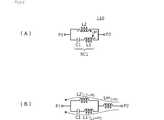
- FIG. 1A is a circuit diagram of the resonance circuit 110 according to the first embodiment.
- FIG. 1B is an equivalent circuit diagram of the resonance circuit 110.
- FIG. 2 is a cross-sectional view of the main part of the resonance circuit 110.
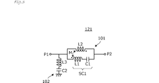
- FIG. 3 is a circuit diagram of the band rejection filter 121 according to the second embodiment.
- FIG. 4A is a diagram showing the pass characteristics and reflection characteristics of the band rejection filter 121.
- FIG. 4B is an enlarged view of the transient region from the stop region to the pass region of FIG.
- FIG. 5 is an external perspective view of the band rejection filter 121 of this embodiment.
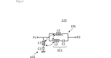
- FIG. 6 is a circuit diagram of another band rejection filter 122 of the present embodiment.
- FIG. 7 is a circuit diagram of another band rejection filter 123 of this embodiment.
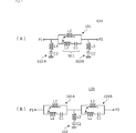
- FIG. 8A and 8B are circuit diagrams of other band rejection filters 124 and 125 according to this embodiment.
- FIG. 9 is a circuit diagram of the band-pass filter 131 according to the third embodiment.
- FIG. 10A is a diagram showing the pass characteristics and reflection characteristics of the band pass filter 131.
- FIG. 10B is an enlarged view of the transition region from the stop region to the pass region of FIG.
- FIG. 11 is a circuit diagram of another band pass filter 132 of the present embodiment.
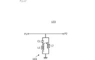
- FIG. 12 is a circuit diagram of another band pass filter 133 of the present embodiment.
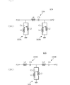
- 13A and 13B are circuit diagrams of other band pass filters 134 and 135 of the present embodiment.
- FIG. 14 is a circuit diagram showing a configuration example of a conventional band rejection filter.
- FIG. 15 is a circuit diagram showing a configuration example of a conventional bandpass filter.
- FIG. 1A is a circuit diagram of the resonance circuit 110 according to the first embodiment.
- the resonance circuit 110 includes a first inductor L1 and a first capacitor C1 that constitute the first series circuit SC1, and a second inductor L2 connected in parallel to the first series circuit SC1. This circuit connected in parallel is connected between the port P1 and the port P2.
- the first inductor L1 and the second inductor L2 couple the magnetic fluxes passing through the first inductor L1 and the second inductor L2 through a magnetic field in a direction in which they mutually strengthen. Therefore, as shown in FIG. 1A, a mutual inductance M is generated due to the coupling of the first inductor L1 and the second inductor L2.
- FIG. 1B is an equivalent circuit diagram of the resonance circuit 110.
- inductors L1 ′, L2 ′, and Lm are inductors obtained by equivalently converting the first inductor L1, the second inductor L2, and the mutual inductance M shown in FIG. It is.
- the inductance of the first inductor L1 is represented by L1
- the inductance of the second inductor L2 by L2
- the mutual inductance by M the inductance of the inductor L1 ′ is (L1 + M)
- the inductance of the inductor L2 ′ is (L2 + M)
- the inductance of the inductor Lm is ( ⁇ M).
- the effective inductance of the first inductor L1 and the second inductor L2 increases due to the coupling of the first inductor L1 and the second inductor L2. Therefore, the inductance of the first inductor L1 and the second inductor L2 alone can be reduced. Accordingly, the resistance component (DC resistance DCR) is reduced, the resistance component of the parallel resonance circuit is reduced, and the Q value is improved.
- the amount of change in reactance with respect to the frequency of the first series circuit SC1 increases, so that the value of the first capacitor C1 can be reduced, and the multilayer structure
- the reactance of the first capacitor C1 portion is represented by -1 / ⁇ C
- the reactance becomes ⁇ L1-1 / ⁇ C1
- the reactance increases.
- This is an effect similar to that of -1 / ⁇ C1 in which the value of C1 increases and reactance increases.
- the inductance of the first inductor L1 is smaller than the inductance of the second inductor L2. Therefore, an increase in the resistance component in the first series circuit SC1 is suppressed, and attenuation of a signal flowing through the first series circuit SC1 is suppressed.
- FIG. 2 is a cross-sectional view of the main part of the resonance circuit 110.
- the first inductor L1 is composed of the first coil conductor 11, and the second inductor L2 is composed of the second coil conductor 12.
- the first coil conductor 11 and the second coil conductor 12 are each composed of a conductor pattern and interlayer connection conductors formed on a plurality of dielectric layers.
- the plurality of dielectric layers are laminated to form a multilayer substrate 50. That is, the first inductor L1 and the second inductor L2 are integrally formed on the multilayer substrate 50.
- the first coil conductor 11 and the second coil conductor 12 have a rectangular helical shape.
- the first coil conductor 11 and the second coil conductor 12 share the coil axis CA, and the inner and outer diameter dimensions of the first coil conductor 11 and the second coil conductor 12 are substantially the same.
- FIG. 2 shows a region where the first inductor L1 and the second inductor L2 are formed.
- One end Tc of the first coil conductor 11 is electrically connected to the electrode of the first capacitor C1. Further, the first end T1 of the second coil conductor 12 is conducted to the first port P1, and the second end T2 of the second coil conductor 12 is conducted to the second port P2.
- the first coil conductor 11 and the second coil conductor 12 share the coil axis CA, and the inner and outer diameters of the first coil conductor 11 and the second coil conductor 12 are substantially the same.
- a resonance circuit having a large mutual inductance M is configured by coupling the first inductor L1 and the second inductor L2.
- the first capacitor C1 may be built in the multilayer substrate 50 or mounted (surface mounted) on the multilayer substrate 50.
- Second Embodiment >> In the second embodiment, examples of some band rejection filters will be described.
- FIG. 3 is a circuit diagram of the band rejection filter 121 according to the second embodiment.
- the band rejection filter 121 includes a first port P1 and a second port P2, and includes a first resonance circuit 101 connected between the first port P1 and the second port P2. Further, a second resonance circuit 102 is provided which is connected between the first port P1 and the ground and is a series circuit of a third inductor L3 and a second capacitor C2.
- the configuration of the first resonance circuit 101 is the same as that of the resonance circuit 110 shown in the first embodiment.
- the effective inductance of the first inductor L1 and the second inductor L2 is increased by the coupling of the first inductor L1 and the second inductor L2. Therefore, the inductance of the first inductor L1 and the second inductor L2 alone can be reduced. Accordingly, the resistance component (DC resistance DCR) is reduced, the resistance component of the parallel resonance circuit is reduced, and the Q value is improved. Therefore, the steepness of the transition region between the stop region end and the pass region end is improved.
- the second resonance circuit by the series circuit of the third inductor L3 and the second capacitor C2 is further provided between the first port P1 and the ground, so that a wide rejection bandwidth is ensured. it can.
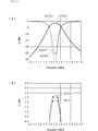
- FIG. 4A is a diagram showing the pass characteristics and reflection characteristics of the band rejection filter 121.
- S21 (E) represents the insertion loss of the band rejection filter 121 of the present embodiment as S parameter S21
- S22 (E) represents the reflection loss of the band rejection filter 121 of the present embodiment as S parameter S22.
- S21 (C) represents the insertion loss of the band rejection filter of the comparative example as S parameter S21
- S22 (C) represents the reflection loss of the band rejection filter of the comparative example as S22. is there.
- each element of the band rejection filter 121 is as follows.
- FIG. 4 (B) is an enlarged view of the transition region from the stop region to the pass region of FIG. 4 (A) for S21 (E) and S21 (C).
- Both the band rejection filter 121 of this embodiment and the band rejection filter of the comparative example are designed with ⁇ 50 MHz as a stop band centered on 1.5 GHz and a pass band in a frequency range that is 150 MHz or more away from the center frequency.
- the comparison was made by designing S21 in the stopband to be -18 dB or less and maximizing S21 in the passband.
- the band rejection filter 121 of the present embodiment shows an improvement of S21 of about 0.2 dB in the pass band.
- FIG. 5 is an external perspective view of the band rejection filter 121 of the present embodiment.
- the band rejection filter 121 includes a first port (terminal) P1, a second port (terminal) P2, and a ground terminal GND.
- the first resonance circuit 101 and the second resonance circuit 102 shown in FIG. 3 are each integrally provided on a multilayer substrate 50 in which a plurality of dielectric layers are stacked.
- the inner and outer diameter dimensions of the first coil conductor and the second coil conductor are substantially the same, and the first coil conductor and the second coil conductor share the coil axis.
- the third inductor L 3 of the second resonance circuit 102 is also provided in the multilayer substrate 50.
- the first capacitor C1 and the second capacitor C2 are also formed on the multilayer substrate 50 by a conductor pattern.
- the first capacitor C1 and the second capacitor C2 may be mounted (surface mounted) on the multilayer substrate 50.
- FIG. 6 is a circuit diagram of another band rejection filter 122 of the present embodiment.
- the band rejection filter 122 has a first port P1 and a second port P2, and includes a first resonance circuit 101 and a second resonance circuit 102.
- the third inductor L3 is coupled to the first inductor L1 and the second inductor L2.
- FIG. 7 is a circuit diagram of another band rejection filter 123 of the present embodiment.
- the band rejection filter 123 includes a first port P1 and a second port P2, and includes a first resonance circuit 101 connected in series.
- the configuration of the first resonance circuit 101 is the same as that of the resonance circuit 110 shown in the first embodiment.
- the band stop filter may be configured with only one LC parallel resonance circuit in this way.
- the band rejection filter 124 has a first port P1 and a second port P2, and one first resonance circuit 101 and two second resonance circuits 102A and 102B are ⁇ -type connected.
- the band rejection filter 125 has a first port P1 and a second port P2, and two first resonance circuits 101A and 101B and one second resonance circuit 102 are T-shaped connected.
- three or more resonant circuits may be connected in multiple stages in this way.
- FIG. 9 is a circuit diagram of the band-pass filter 131 according to the third embodiment.
- the band pass filter 131 has a first port P1 and a second port P2, and is connected in series between the third resonance circuit 103 shunt-connected to the first port P1 and between the first port P1 and the second port P2.
- the fourth resonance circuit 104 is provided.
- the configuration of the third resonance circuit 103 is the same as that of the resonance circuit 110 shown in the first embodiment.
- the fourth resonance circuit 104 includes a series circuit of a fourth inductor L4 and a third capacitor C3.
- FIG. 10A is a diagram showing the pass characteristics and reflection characteristics of the band pass filter 131.
- S21 (E) represents the insertion loss of the band-pass filter 131 of this embodiment as S parameter S21
- S22 (E) represents the reflection loss of the band-pass filter 131 of this embodiment as S parameter S22. It is represented by.
- S21 (C) is the insertion loss of the bandpass filter of the comparative example represented by S parameter S21
- S22 (C) is the reflection loss of the bandpass filter of the comparative example represented by S22 of S parameter. is there.
- each element of the band pass filter 131 is as follows.
- the band-pass filter of the comparative example is L1: 0nH, C3: 18.8pF.
- FIG. 10 (B) is an enlarged view of the transition region from the stop region to the pass region of FIG. 10 (A) for S21 (E) and S21 (C).
- Both the bandpass filter 131 of this embodiment and the bandpass filter of the comparative example are designed with a passband of ⁇ 50 MHz centered on 1.5 GHz and a stopband in a frequency range that is 150 MHz or more away from the center frequency.
- a comparison was made by designing S21 in the stopband to be ⁇ 10 dB or less and maximizing S21 in the passband.
- the bandpass filter 131 of the present embodiment shows an improvement of S21 of about 0.4 dB in the passband.
- FIG. 11 is a circuit diagram of another band pass filter 132 of the present embodiment.
- the band pass filter 132 has a first port P1 and a second port P2, and includes a third resonance circuit 103 and a fourth resonance circuit 104.
- the fourth inductor L4 is coupled to the first inductor L1 and the second inductor L2.
- FIG. 12 is a circuit diagram of another band pass filter 133 of the present embodiment.
- the band pass filter 133 has a first port P1 and a second port P2, and includes a third resonance circuit 103 that is shunt-connected.
- the configuration of the third resonance circuit 103 is the same as that of the resonance circuit 110 shown in the first embodiment.
- the band pass filter may be configured by only one stage of the LC parallel resonance circuit.
- FIGS. 13A and 13B are circuit diagrams of other band pass filters 134 and 135 of the present embodiment.
- the bandpass filter 134 has a first port P1 and a second port P2, and two third resonance circuits 103A and 103B and one fourth resonance circuit 104 are ⁇ -type connected.
- the band pass filter 135 includes a first port P1 and a second port P2, and one third resonance circuit 103 and two fourth resonance circuits 104A and 104B are T-connected.
- three or more resonant circuits may be connected in multiple stages in this way.
- the first capacitor C1, the second capacitor C2, and the third capacitor C3 are mounted on a printed wiring board as separate components, in addition to being integrally provided inside and outside the multilayer substrate. Also good.
Landscapes
- Engineering & Computer Science (AREA)
- Power Engineering (AREA)
- Physics & Mathematics (AREA)
- Acoustics & Sound (AREA)
- Filters And Equalizers (AREA)
Abstract
第1共振回路(101)は、例えば、第1直列回路(SC1)を構成する第1インダクタ(L1)および第1キャパシタ(C1)と、第1直列回路(SC1)に並列接続される第2インダクタ(L2)とを備え、第1インダクタ(L1)と第2インダクタ(L2)とは、第1インダクタ(L1)および第2インダクタ(L2)を通る磁束を互いに強め合う方向に磁界を介して結合し、過渡域の急峻性を効果的に高める。
Description
本発明は、インダクタおよびキャパシタを備える共振回路、この共振回路を含む帯域阻止フィルタおよび帯域通過フィルタに関する。
従来、高周波回路に備えられる帯域阻止フィルタや帯域通過フィルタには、LC並列共振回路が備えられる。例えば、図14に示すように、信号経路にシリーズ接続されるLC並列回路と信号経路とグランドとの間にシャント接続されるLC直列回路とで帯域阻止フィルタが構成される。また、図15に示すように、信号経路にシリーズ接続されるLC直列回路と信号経路とグランドとの間にシャント接続されるLC並列回路とで帯域通過フィルタが構成される。
図14に示した帯域阻止フィルタは例えば特許文献1に示されている。また、図15に示した帯域通過フィルタは例えば特許文献2に示されている。
一般に、帯域阻止フィルタや帯域通過フィルタにおいて、阻止域端と通過域端との間の過渡域に急峻性が要求される場合、シリーズに接続される素子数およびシャントに接続される素子数を増やすことが有効であるが、それに伴い、挿入損失が増加する問題がある。
図14、図15に示すように、LC共振回路を備えるフィルタにおいては、LC共振回路のQ値を高めることによって、過渡域の急峻性を高めることができる。しかし、インダクタの直流抵抗(DCR)およびキャパシタの等価直列抵抗(ESR)はいずれもそれらの構造と導電材料によって定まり、LC共振回路のQ値を効果的に高めることはできなかった。
本発明の目的は、過渡域の急峻性を効果的に高められるようにした共振回路、帯域阻止フィルタ、および帯域通過フィルタを提供することにある。
(1)本発明の共振回路は、
第1直列回路を構成する第1インダクタおよび第1キャパシタと、前記第1直列回路に並列接続される第2インダクタとを備え、
前記第1インダクタと前記第2インダクタとは、前記第1インダクタおよび前記第2インダクタを通る磁束を互いに強め合う方向に磁界を介して結合していることを特徴とする。
第1直列回路を構成する第1インダクタおよび第1キャパシタと、前記第1直列回路に並列接続される第2インダクタとを備え、
前記第1インダクタと前記第2インダクタとは、前記第1インダクタおよび前記第2インダクタを通る磁束を互いに強め合う方向に磁界を介して結合していることを特徴とする。
上記構成により、第1インダクタおよび第2インダクタの実効的なインダクタンスが大きくなるため、単体でのインダクタンスを小さくできる。このことにより、並列共振回路の抵抗成分が減少して、そのQ値が向上する。
(2)上記(1)において、前記第1インダクタのインダクタンスは前記第2インダクタのインダクタンスよりも小さいことが好ましい。これにより、第1直列回路での抵抗成分の増加が抑えられ、この第1直列回路を流れる信号の減衰が抑制される。
(3)上記(1)または(2)において、前記第1インダクタは第1コイル導体、前記第2インダクタは第2コイル導体でそれぞれ構成され、前記第1コイル導体および前記第2コイル導体は、複数の誘電体層が積層された多層基板に一体的に構成され、前記第1コイル導体および前記第2コイル導体の内外径寸法は実質的に同じであり、前記第1コイル導体および前記第2コイル導体はコイル軸を共有することが好ましい。これにより、小型でありながら、第1インダクタと第2インダクタとの結合による相互インダクタンスの大きな共振回路が構成される。
(4)本発明の帯域阻止フィルタは、
第1ポートおよび第2ポートを有し、第1直列回路を構成する第1インダクタおよび第1キャパシタと、前記第1直列回路に並列接続される第2インダクタとが、前記第1ポートと前記第2ポートとの間に接続された第1共振回路を備え、前記第1インダクタと前記第2インダクタとは、前記第1インダクタおよび前記第2インダクタを通る磁束を互いに強め合う方向に磁界を介して結合していることを特徴とする。
第1ポートおよび第2ポートを有し、第1直列回路を構成する第1インダクタおよび第1キャパシタと、前記第1直列回路に並列接続される第2インダクタとが、前記第1ポートと前記第2ポートとの間に接続された第1共振回路を備え、前記第1インダクタと前記第2インダクタとは、前記第1インダクタおよび前記第2インダクタを通る磁束を互いに強め合う方向に磁界を介して結合していることを特徴とする。
上記構成により、第1インダクタおよび第2インダクタの実効的なインダクタンスが大きくなるため、単体でのインダクタンスを小さくでき、そのことにより、並列共振回路の抵抗成分が減少して、そのQ値が向上する。したがって、阻止域端と通過域端との間の過渡域の急峻性が向上する。
(5)上記(4)において、前記第1インダクタのインダクタンスは前記第2インダクタのインダクタンスよりも小さいことが好ましい。これにより、第1直列回路での抵抗成分の増加が抑えられ、この第1直列回路を流れる信号の減衰が抑制される。すなわち、第1インダクタを設けたことによる、通過域での挿入損失の増大が抑えられる。
(6)上記(4)または(5)において、前記第1ポートとグランドとの間に接続され、第3インダクタを含む第2共振回路を更に備えることが好ましい。これにより、広い阻止帯域幅を確保できる。
(7)上記(6)において、前記第1インダクタおよび前記第2インダクタは前記第3インダクタと互いに結合することが好ましい。これにより、共振回路の抵抗成分が減少してQ値が向上し、阻止帯域端と通過域端との間の過渡域の急峻性が向上する。
(8)上記(4)から(7)のいずれかにおいて、前記第1インダクタは第1コイル導体、前記第2インダクタは第2コイル導体でそれぞれ構成され、前記第1コイル導体および前記第2コイル導体は、複数の誘電体層が積層された多層基板に一体的に構成され、前記第1コイル導体および前記第2コイル導体の内外径寸法は実質的に同じであり、前記第1コイル導体および前記第2コイル導体はコイル軸を共有することが好ましい。これにより、小型でありながら、第1インダクタおよび第2インダクタの実効的なインダクタンスが大きくなって、過渡域の急峻性向上効果が高まる。
(9)本発明の帯域通過フィルタは、
第1ポートおよび第2ポートを有し、第1直列回路を構成する第1インダクタおよび第1キャパシタと、前記第1直列回路に並列接続される第2インダクタとが、前記第1ポートとグランドとの間に接続された第3共振回路を備え、前記第1インダクタと前記第2インダクタとは、前記第1インダクタおよび前記第2インダクタを通る磁束を互いに強め合う方向に磁界を介して結合していることを特徴とする。
第1ポートおよび第2ポートを有し、第1直列回路を構成する第1インダクタおよび第1キャパシタと、前記第1直列回路に並列接続される第2インダクタとが、前記第1ポートとグランドとの間に接続された第3共振回路を備え、前記第1インダクタと前記第2インダクタとは、前記第1インダクタおよび前記第2インダクタを通る磁束を互いに強め合う方向に磁界を介して結合していることを特徴とする。
上記構成により、第1インダクタおよび第2インダクタの実効的なインダクタンスが大きくなるため、単体でのインダクタンスを小さくでき、そのことにより、並列共振回路の抵抗成分が減少して、そのQ値が向上する。したがって、阻止域端と通過域端との間の過渡域の急峻性が向上する。
(10)上記(9)において、前記第1インダクタのインダクタンスは前記第2インダクタのインダクタンスよりも小さいことが好ましい。これにより、第1直列回路での抵抗成分の増加が抑えられる。すなわち、第1インダクタを設けたことによる、減衰域での減衰量の減少が抑えられる。
(11)上記(10)において、前記第1ポートと前記第2ポートとの間に接続され、第4インダクタを含む第4共振回路を更に備ることが好ましい。これにより、広い通過帯域幅を確保できる。
(12)上記(11)において、前記第1インダクタおよび前記第2インダクタは前記第4インダクタと互いに結合することが好ましい。これにより、共振回路の抵抗成分が減少してQ値が向上し、阻止帯域端と通過域端との間の過渡域の急峻性が向上する。
(13)上記(9)から(12)のいずれかにおいて、前記第1インダクタは第1コイル導体、前記第2インダクタは第2コイル導体でそれぞれ構成され、前記第1コイル導体および前記第2コイル導体は、複数の誘電体層が積層された多層基板に一体的に構成され、前記第1コイル導体および前記第2コイル導体の内外径寸法は実質的に同じであり、前記第1コイル導体および前記第2コイル導体はコイル軸を共有することが好ましい。これにより、小型でありながら、第1インダクタおよび第2インダクタの実効的なインダクタンスが大きくなって、過渡域の急峻性向上効果が高まる。
本発明によれば、Q値の高い共振回路、阻止域端と通過域端との間の過渡域の急峻性の高い帯域阻止フィルタまたは帯域通過フィルタが得られる。
以降、図を参照して幾つかの具体的な例を挙げて、本発明を実施するための複数の形態を示す。各図中には同一箇所に同一符号を付している。要点の説明または理解の容易性を考慮して、便宜上実施形態を分けて示すが、異なる実施形態で示した構成の部分的な置換または組み合わせが可能である。第2の実施形態以降では第1の実施形態と共通の事柄についての記述を省略し、異なる点についてのみ説明する。特に、同様の構成による同様の作用効果については実施形態毎には逐次言及しない。
《第1の実施形態》
第1の実施形態では共振回路について示す。
第1の実施形態では共振回路について示す。
図1(A)は第1の実施形態に係る共振回路110の回路図である。この共振回路110は、第1直列回路SC1を構成する第1インダクタL1および第1キャパシタC1と、第1直列回路SC1に並列接続される第2インダクタL2とを備える。この並列接続された回路はポートP1とポートP2との間に接続されている。
第1インダクタL1と第2インダクタL2とは、第1インダクタL1および第2インダクタL2を通る磁束を互いに強め合う方向に磁界を介して結合する。そのため、図1(A)中に示すように、第1インダクタL1と第2インダクタL2との結合による相互インダクタンスMが生じる。
図1(B)は共振回路110の等価回路図である。図1(B)において、インダクタL1′,L2′,Lmは、図1(A)に示した、第1インダクタL1、第2インダクタL2および相互インダクタンスMをT型回路に等価変換したことによるインダクタである。ここで、第1インダクタL1のインダクタンスをL1、第2インダクタL2のインダクタンスをL2、相互インダクタンスをMで表すと、インダクタL1′のインダクタンスは(L1+M)、インダクタL2′のインダクタンスは(L2+M)、インダクタLmのインダクタンスは(-M)である。このように、第1インダクタL1と第2インダクタL2との結合により、第1インダクタL1および第2インダクタL2の実効的なインダクタンスは大きくなる。そのため、第1インダクタL1および第2インダクタL2の単体でのインダクタンスは小さくできる。それに伴い、抵抗成分(直流抵抗DCR)が小さくなり、並列共振回路の抵抗成分が減少して、そのQ値が向上する。
また、第1キャパシタC1に対して直列に第1インダクタL1を接続することにより、第1直列回路SC1の、周波数に対するリアクタンス変化量が増加するので、第1キャパシタC1の値を小さくでき、積層構造で一体化する際に作製が容易になるメリットがある。すなわち、第1キャパシタC1部分のリアクタンスは-1/ωCで表され、これに直列に小さなインダクタンスの第1インダクタL1が入った場合のリアクタンスは、ωL1-1/ωC1となり、リアクタンスは増加する。これは、-1/ωC1の、C1の値が大きくなってリアクタンスが増加することに近い効果である。これにより、実質的なキャパシタンスの値が増えたことにほぼ等価となり、第1キャパシタC1のキャパシタンスを減らすことができる。
第1インダクタL1のインダクタンスは第2インダクタL2のインダクタンスよりも小さいことが好ましい。これにより、第1直列回路SC1での抵抗成分の増加が抑えられ、この第1直列回路SC1を流れる信号の減衰が抑制される。
図2は共振回路110の主要部の断面図である。第1インダクタL1は第1コイル導体11、第2インダクタL2は第2コイル導体12でそれぞれ構成される。第1コイル導体11および第2コイル導体12は、それぞれ複数の誘電体層に形成された導体パターンと層間接続導体とで構成される。これら複数の誘電体層は積層されて多層基板50が構成される。すなわち、多層基板50に第1インダクタL1および第2インダクタL2が一体的に構成されている。第1コイル導体11および第2コイル導体12は矩形ヘリカル状である。第1コイル導体11および第2コイル導体12はコイル軸CAを共有し、第1コイル導体11および第2コイル導体12の内外径寸法は実質的に同じである。
図2においては、第1インダクタL1および第2インダクタL2の形成領域について示している。第1コイル導体11の一端部Tcは第1キャパシタC1の電極に導通する。また、第2コイル導体12の第1端T1は第1ポートP1に導通し、第2コイル導体12の第2端T2は第2ポートP2に導通する。
上述のとおり、第1コイル導体11および第2コイル導体12はコイル軸CAを共有し、第1コイル導体11および第2コイル導体12の内外径寸法は実質的に同じであるので、小型でありながら、第1インダクタL1と第2インダクタL2との結合による相互インダクタンスMの大きな共振回路が構成される。
上記第1キャパシタC1は多層基板50に内蔵してもよいし、多層基板50に搭載(表面実装)してもよい。
《第2の実施形態》
第2の実施形態では、幾つかの帯域阻止フィルタの例について示す。
第2の実施形態では、幾つかの帯域阻止フィルタの例について示す。
図3は第2の実施形態に係る帯域阻止フィルタ121の回路図である。帯域阻止フィルタ121は、第1ポートP1および第2ポートP2を有し、この第1ポートP1と第2ポートP2との間に接続された第1共振回路101を備える。更に、第1ポートP1とグランドとの間に接続され、第3インダクタL3と第2キャパシタC2との直列回路による第2共振回路102を備える。
第1共振回路101の構成は第1の実施形態で示した共振回路110と同じである。
上記構成により、第1インダクタL1と第2インダクタL2の結合により、第1インダクタL1および第2インダクタL2の実効的なインダクタンスは大きくなる。そのため、第1インダクタL1および第2インダクタL2の単体でのインダクタンスは小さくできる。それに伴い、抵抗成分(直流抵抗DCR)が小さくなり、並列共振回路の抵抗成分が減少して、そのQ値が向上する。したがって、阻止域端と通過域端との間の過渡域の急峻性が向上する。
また、帯域阻止フィルタ121によれば、第1ポートP1とグランドとの間に、第3インダクタL3と第2キャパシタC2との直列回路による第2共振回路を更に備えるので、広い阻止帯域幅を確保できる。
図4(A)は帯域阻止フィルタ121の通過特性および反射特性を示す図である。ここで、S21(E)は本実施形態の帯域阻止フィルタ121の挿入損失をSパラメータのS21で表したもの、S22(E)は本実施形態の帯域阻止フィルタ121の反射損失をSパラメータのS22で表したものである。また、S21(C)は比較例の帯域阻止フィルタの挿入損失をSパラメータのS21で表したもの、S22(C)は比較例の帯域阻止フィルタの反射損失をSパラメータのS22で表したものである。
帯域阻止フィルタ121の各素子の値は次のとおりである。
L1:0.8nH
L2:1.1nH
L3:29nH
C1:3.5pF
C2:0.4pF
結合係数k:0.8
比較例の帯域阻止フィルタは、L1:0nH、C1:10.9pFとしたものである。
L2:1.1nH
L3:29nH
C1:3.5pF
C2:0.4pF
結合係数k:0.8
比較例の帯域阻止フィルタは、L1:0nH、C1:10.9pFとしたものである。
図4(B)は、S21(E)、S21(C)について、図4(A)の阻止域から通過域にかけての過渡域を拡大した図である。
本実施形態の帯域阻止フィルタ121も比較例の帯域阻止フィルタも、1.5GHzを中心に±50MHzを阻止帯域とし、中心周波数から150MHz以上離れた周波数域を通過帯域として設計されている。ここでは、阻止帯域のS21を-18dB以下となるようして、通過帯域のS21が最大となるように設計して比較を行った。
図4(A)(B)から明らかなように、本実施形態の帯域阻止フィルタ121では、通過帯域で約0.2dBのS21の改善がみられる。
図5は本実施形態の帯域阻止フィルタ121の外観斜視図である。帯域阻止フィルタ121は、第1ポート(端子)P1、第2ポート(端子)P2およびグランド端子GNDを備える。図3に示した第1共振回路101および第2共振回路102は、それぞれ複数の誘電体層が積層された多層基板50に一体的に設けられている。第1コイル導体および第2コイル導体の内外径寸法は実質的に同じであり、第1コイル導体および第2コイル導体はコイル軸を共有する。第2共振回路102の第3インダクタL3も多層基板50内に設けられている。第1キャパシタC1、第2キャパシタC2も多層基板50に導体パターンによって形成されている。第1キャパシタC1、第2キャパシタC2は多層基板50に搭載(表面実装)してもよい。
図6は本実施形態の別の帯域阻止フィルタ122の回路図である。帯域阻止フィルタ122は、第1ポートP1および第2ポートP2を有し、第1共振回路101および第2共振回路102を備える。図3に示した帯域阻止フィルタ121と異なり、第3インダクタL3は第1インダクタL1および第2インダクタL2と結合する。これにより、共振回路の抵抗成分が減少してQ値が向上し、阻止帯域端と通過域端との間の過渡域の急峻性が向上する。
図7は本実施形態の別の帯域阻止フィルタ123の回路図である。帯域阻止フィルタ123は、第1ポートP1および第2ポートP2を有し、シリーズ接続された第1共振回路101を備える。第1共振回路101の構成は第1の実施形態で示した共振回路110と同じである。阻止帯域幅が狭い場合には、このように1段のLC並列共振回路だけで帯域阻止フィルタを構成してもよい。
図8(A)(B)は本実施形態の別の帯域阻止フィルタ124,125の回路図である。帯域阻止フィルタ124は、第1ポートP1および第2ポートP2を有し、1つの第1共振回路101と2つの第2共振回路102A,102Bとがπ型接続されている。また、帯域阻止フィルタ125は、第1ポートP1および第2ポートP2を有し、2つの第1共振回路101A,101Bと1つの第2共振回路102とがT型接続されている。
通過域での挿入損失が許容値以内であれば、このように3つまたはそれ以上の共振回路を多段接続してもよい。
《第3の実施形態》
第3の実施形態では、幾つかの帯域通過フィルタの例について示す。
第3の実施形態では、幾つかの帯域通過フィルタの例について示す。
図9は第3の実施形態に係る帯域通過フィルタ131の回路図である。帯域通過フィルタ131は、第1ポートP1および第2ポートP2を有し、第1ポートP1にシャント接続された第3共振回路103、および第1ポートP1と第2ポートP2との間にシリーズ接続された第4共振回路104を備える。
第3共振回路103の構成は第1の実施形態で示した共振回路110と同じである。第4共振回路104は第4インダクタL4と第3キャパシタC3との直列回路で構成される。
図10(A)は帯域通過フィルタ131の通過特性および反射特性を示す図である。ここで、S21(E)は本実施形態の帯域通過フィルタ131の挿入損失をSパラメータのS21で表したもの、S22(E)は本実施形態の帯域通過フィルタ131の反射損失をSパラメータのS22で表したものである。また、S21(C)は比較例の帯域通過フィルタの挿入損失をSパラメータのS21で表したもの、S22(C)は比較例の帯域通過フィルタの反射損失をSパラメータのS22で表したものである。
帯域通過フィルタ131の各素子の値は次のとおりである。
L1:1.2nH
L2:0.6nH
L4:40nH
C1:0.3pF
C3:5.2pF
結合係数k:0.8
比較例の帯域通過フィルタは、L1:0nH、C3:18.8pFとしたものである。
L2:0.6nH
L4:40nH
C1:0.3pF
C3:5.2pF
結合係数k:0.8
比較例の帯域通過フィルタは、L1:0nH、C3:18.8pFとしたものである。
図10(B)は、S21(E)、S21(C)について、図10(A)の阻止域から通過域にかけての過渡域を拡大した図である。
本実施形態の帯域通過フィルタ131も比較例の帯域通過フィルタも、1.5GHzを中心に±50MHzを通過帯域とし、中心周波数から150MHz以上離れた周波数域を阻止帯域として設計されている。ここでは、阻止帯域のS21を-10dB以下となるようして、通過帯域のS21が最大となるように設計して比較を行った。
図10(A)(B)から明らかなように、本実施形態の帯域通過フィルタ131では、通過帯域で約0.4dBのS21の改善がみられる。
図11は本実施形態の別の帯域通過フィルタ132の回路図である。帯域通過フィルタ132は、第1ポートP1および第2ポートP2を有し、第3共振回路103および第4共振回路104を備える。図9に示した帯域通過フィルタ131と異なり、第4インダクタL4は第1インダクタL1および第2インダクタL2と結合する。これにより、共振回路の抵抗成分が減少してQ値が向上し、阻止帯域端と通過域端との間の過渡域の急峻性が向上する。
図12は本実施形態の別の帯域通過フィルタ133の回路図である。帯域通過フィルタ133は、第1ポートP1および第2ポートP2を有し、シャント接続された第3共振回路103を備える。第3共振回路103の構成は第1の実施形態で示した共振回路110と同じである。通過帯域幅が狭い場合には、このように1段のLC並列共振回路だけで帯域通過フィルタを構成してもよい。
図13(A)(B)は本実施形態の別の帯域通過フィルタ134,135の回路図である。帯域通過フィルタ134は、第1ポートP1および第2ポートP2を有し、2つの第3共振回路103A,103Bと1つの第4共振回路104とがπ型接続されている。また、帯域通過フィルタ135は、第1ポートP1および第2ポートP2を有し、1つの第3共振回路103と2つの第4共振回路104A,104BとがT型接続されている。
通過域での挿入損失が許容値以内であれば、このように3つまたはそれ以上の共振回路を多段接続してもよい。
なお、以上に示した各実施形態では、第1キャパシタC1、第2キャパシタC2、第3キャパシタC3は、多層基板の内外に一体的に設けること以外に、別部品としてプリント配線板に実装してもよい。
最後に、上述の実施形態の説明は、すべての点で例示であって、制限的なものではない。当業者にとって変形および変更が適宜可能である。例えば、異なる実施形態で示した構成の部分的な置換または組み合わせが可能である。本発明の範囲は、上述の実施形態ではなく、特許請求の範囲によって示される。さらに、本発明の範囲には、特許請求の範囲と均等の意味および範囲内でのすべての変更が含まれることが意図される。
C1…第1キャパシタ
C2…第2キャパシタ
C3…第3キャパシタ
CA…コイル軸
GND…グランド端子
L1…第1インダクタ
L2…第2インダクタ
L3…第3インダクタ
L4…第4インダクタ
P1…第1ポート
P2…第2ポート
SC1…第1直列回路
11…第1コイル導体
12…第2コイル導体
50…多層基板
101,101A,101B…第1共振回路
102,102A,102B…第2共振回路
103,103A,103B…第3共振回路
104,104A,104B…第4共振回路
110…共振回路
121~125…帯域阻止フィルタ
131~135…帯域通過フィルタ
C2…第2キャパシタ
C3…第3キャパシタ
CA…コイル軸
GND…グランド端子
L1…第1インダクタ
L2…第2インダクタ
L3…第3インダクタ
L4…第4インダクタ
P1…第1ポート
P2…第2ポート
SC1…第1直列回路
11…第1コイル導体
12…第2コイル導体
50…多層基板
101,101A,101B…第1共振回路
102,102A,102B…第2共振回路
103,103A,103B…第3共振回路
104,104A,104B…第4共振回路
110…共振回路
121~125…帯域阻止フィルタ
131~135…帯域通過フィルタ
Claims (13)
- 第1直列回路を構成する第1インダクタおよび第1キャパシタと、前記第1直列回路に並列接続される第2インダクタとを備え、
前記第1インダクタと前記第2インダクタとは、前記第1インダクタおよび前記第2インダクタを通る磁束を互いに強め合う方向に磁界を介して結合していることを特徴とする、共振回路。 - 前記第1インダクタのインダクタンスは前記第2インダクタのインダクタンスよりも小さい、請求項1に記載の共振回路。
- 前記第1インダクタは第1コイル導体、前記第2インダクタは第2コイル導体でそれぞれ構成され、
前記第1コイル導体および前記第2コイル導体は、複数の誘電体層が積層された多層基板に一体的に構成され、前記第1コイル導体および前記第2コイル導体の内外径寸法は実質的に同じであり、前記第1コイル導体および前記第2コイル導体はコイル軸を共有する、請求項1または2に記載の共振回路。 - 第1ポートおよび第2ポートを有し、
第1直列回路を構成する第1インダクタおよび第1キャパシタと、前記第1直列回路に並列接続される第2インダクタとが、前記第1ポートと前記第2ポートとの間に接続された第1共振回路を備え、
前記第1インダクタと前記第2インダクタとは、前記第1インダクタおよび前記第2インダクタを通る磁束を互いに強め合う方向に磁界を介して結合していることを特徴とする、帯域阻止フィルタ。 - 前記第1インダクタのインダクタンスは前記第2インダクタのインダクタンスよりも小さい、請求項4に記載の帯域阻止フィルタ。
- 前記第1ポートとグランドとの間に接続され、第3インダクタを含む第2共振回路を更に備える、請求項4または5に記載の帯域阻止フィルタ。
- 前記第1インダクタおよび前記第2インダクタは前記第3インダクタと互いに結合する、請求項6に記載の帯域阻止フィルタ。
- 前記第1インダクタは第1コイル導体、前記第2インダクタは第2コイル導体でそれぞれ構成され、
前記第1コイル導体および前記第2コイル導体は、複数の誘電体層が積層された多層基板に一体的に構成され、前記第1コイル導体および前記第2コイル導体の内外径寸法は実質的に同じであり、前記第1コイル導体および前記第2コイル導体はコイル軸を共有する、請求項4から7のいずれかに記載の帯域阻止フィルタ。 - 第1ポートおよび第2ポートを有し、
第1直列回路を構成する第1インダクタおよび第1キャパシタと、前記第1直列回路に並列接続される第2インダクタとが、前記第1ポートとグランドとの間に接続された第3共振回路を備え、
前記第1インダクタと前記第2インダクタとは、前記第1インダクタおよび前記第2インダクタを通る磁束を互いに強め合う方向に磁界を介して結合していることを特徴とする、帯域通過フィルタ。 - 前記第1インダクタのインダクタンスは前記第2インダクタのインダクタンスよりも小さい、請求項9に記載の帯域通過フィルタ。
- 前記第1ポートと前記第2ポートとの間に接続され、第4インダクタを含む第4共振回路を更に備る、請求項9または10に記載の帯域通過フィルタ。
- 前記第1インダクタおよび前記第2インダクタは前記第4インダクタと互いに結合する、請求項11に記載の帯域通過フィルタ。
- 前記第1インダクタは第1コイル導体、前記第2インダクタは第2コイル導体でそれぞれ構成され、
前記第1コイル導体および前記第2コイル導体は、複数の誘電体層が積層された多層基板に一体的に構成され、前記第1コイル導体および前記第2コイル導体の内外径寸法は実質的に同じであり、前記第1コイル導体および前記第2コイル導体はコイル軸を共有する、請求項9から12のいずれかに記載の帯域通過フィルタ。
Priority Applications (3)
| Application Number | Priority Date | Filing Date | Title |
|---|---|---|---|
| JP2017512278A JP6531824B2 (ja) | 2015-04-17 | 2016-04-07 | 共振回路、帯域阻止フィルタおよび帯域通過フィルタ |
| CN201680020860.9A CN107431467B (zh) | 2015-04-17 | 2016-04-07 | 谐振电路、带阻滤波器以及带通滤波器 |
| US15/726,477 US10530322B2 (en) | 2015-04-17 | 2017-10-06 | Resonant circuit, band elimination filter, and band pass filter |
Applications Claiming Priority (2)
| Application Number | Priority Date | Filing Date | Title |
|---|---|---|---|
| JP2015085166 | 2015-04-17 | ||
| JP2015-085166 | 2015-04-17 |
Related Child Applications (1)
| Application Number | Title | Priority Date | Filing Date |
|---|---|---|---|
| US15/726,477 Continuation US10530322B2 (en) | 2015-04-17 | 2017-10-06 | Resonant circuit, band elimination filter, and band pass filter |
Publications (1)
| Publication Number | Publication Date |
|---|---|
| WO2016167171A1 true WO2016167171A1 (ja) | 2016-10-20 |
Family
ID=57126438
Family Applications (1)
| Application Number | Title | Priority Date | Filing Date |
|---|---|---|---|
| PCT/JP2016/061348 Ceased WO2016167171A1 (ja) | 2015-04-17 | 2016-04-07 | 共振回路、帯域阻止フィルタおよび帯域通過フィルタ |
Country Status (4)
| Country | Link |
|---|---|
| US (1) | US10530322B2 (ja) |
| JP (1) | JP6531824B2 (ja) |
| CN (1) | CN107431467B (ja) |
| WO (1) | WO2016167171A1 (ja) |
Cited By (5)
| Publication number | Priority date | Publication date | Assignee | Title |
|---|---|---|---|---|
| WO2018180150A1 (ja) * | 2017-03-29 | 2018-10-04 | 株式会社村田製作所 | トラップフィルタおよびフィルタ回路 |
| WO2019102830A1 (ja) * | 2017-11-22 | 2019-05-31 | 株式会社村田製作所 | バンドパスフィルタ |
| WO2019235261A1 (ja) * | 2018-06-08 | 2019-12-12 | 株式会社村田製作所 | フィルタ素子 |
| JP2020195009A (ja) * | 2019-05-24 | 2020-12-03 | 株式会社村田製作所 | 信号電源分離回路およびそれを用いた信号伝送回路並びに車両 |
| JPWO2023276879A1 (ja) * | 2021-07-02 | 2023-01-05 |
Families Citing this family (3)
| Publication number | Priority date | Publication date | Assignee | Title |
|---|---|---|---|---|
| JP6950754B2 (ja) * | 2018-01-26 | 2021-10-13 | 株式会社村田製作所 | バンドパスフィルタ |
| JP7579074B2 (ja) * | 2020-07-07 | 2024-11-07 | Tdk株式会社 | 積層コイル部品 |
| CN117941254A (zh) | 2021-11-22 | 2024-04-26 | 株式会社村田制作所 | 滤波器装置、天线装置以及天线模块 |
Citations (7)
| Publication number | Priority date | Publication date | Assignee | Title |
|---|---|---|---|---|
| US4451803A (en) * | 1982-06-23 | 1984-05-29 | Eagle Comtronics, Inc. | Split tuning filter |
| JPH02224513A (ja) * | 1989-02-27 | 1990-09-06 | Murata Mfg Co Ltd | Lc複合部品における周波数調整方法 |
| JPH06224644A (ja) * | 1993-01-25 | 1994-08-12 | Nec Corp | 半導体装置 |
| JP2004312741A (ja) * | 2003-04-03 | 2004-11-04 | Stmicroelectronics Sa | 一体型の二帯域インダクタンス及びその応用 |
| WO2005036741A1 (ja) * | 2003-10-14 | 2005-04-21 | Soc Corporation | ノイズ防止コイル回路 |
| JP2006186621A (ja) * | 2004-12-27 | 2006-07-13 | Tdk Corp | フィルタ回路 |
| WO2014185231A1 (ja) * | 2013-05-15 | 2014-11-20 | 株式会社村田製作所 | 信号伝送ケーブル、および通信機器モジュール |
Family Cites Families (17)
| Publication number | Priority date | Publication date | Assignee | Title |
|---|---|---|---|---|
| JPS6318709A (ja) | 1986-07-09 | 1988-01-26 | Matsushita Electric Ind Co Ltd | Lcバンドパスフイルタ |
| JPS63179603A (ja) * | 1987-01-20 | 1988-07-23 | Matsushita Electric Ind Co Ltd | バンドパスフイルタ |
| JPS63222505A (ja) * | 1987-03-11 | 1988-09-16 | Murata Mfg Co Ltd | 共振器 |
| JPH02256218A (ja) * | 1989-03-29 | 1990-10-17 | Murata Mfg Co Ltd | Lc複合部品 |
| US5621366A (en) * | 1994-08-15 | 1997-04-15 | Motorola, Inc. | High-Q multi-layer ceramic RF transmission line resonator |
| US6404279B2 (en) * | 2000-01-26 | 2002-06-11 | Acoustic Technologies, Inc. | Band pass filter with improved group delay |
| US20020152490A1 (en) * | 2001-04-12 | 2002-10-17 | Philip Lake | Tolerance-inducing thy-marrow composite tissue construct and organ |
| EP1450486A1 (en) | 2003-02-20 | 2004-08-25 | TDK Corporation | Multi-Mode Filter |
| US7554423B2 (en) * | 2006-10-24 | 2009-06-30 | Virginia Tech Intellectual Properties, Inc. | Cancellation of inductor winding capacitance |
| JP2012238797A (ja) * | 2011-05-13 | 2012-12-06 | Murata Mfg Co Ltd | 多層回路モジュール |
| JP5573804B2 (ja) * | 2011-09-23 | 2014-08-20 | 株式会社村田製作所 | 帯域通過フィルタ |
| WO2013069498A1 (ja) * | 2011-11-08 | 2013-05-16 | 株式会社村田製作所 | Lcフィルタ回路及び高周波モジュール |
| JP5618027B2 (ja) * | 2012-09-28 | 2014-11-05 | 株式会社村田製作所 | インピーダンス変換回路およびアンテナ装置 |
| WO2014064987A1 (ja) * | 2012-10-24 | 2014-05-01 | 株式会社村田製作所 | フィルタ装置 |
| US20160002835A1 (en) * | 2013-02-12 | 2016-01-07 | Kuraray Co., Ltd. | Hard sheet and method for producing the same |
| CN103259501B (zh) * | 2013-05-31 | 2016-06-29 | 电子科技大学 | 一种通信系统用带阻滤波器 |
| JP5907124B2 (ja) * | 2013-07-24 | 2016-04-20 | 株式会社村田製作所 | 高周波部品およびフィルタ部品 |
-
2016
- 2016-04-07 JP JP2017512278A patent/JP6531824B2/ja active Active
- 2016-04-07 WO PCT/JP2016/061348 patent/WO2016167171A1/ja not_active Ceased
- 2016-04-07 CN CN201680020860.9A patent/CN107431467B/zh active Active
-
2017
- 2017-10-06 US US15/726,477 patent/US10530322B2/en active Active
Patent Citations (7)
| Publication number | Priority date | Publication date | Assignee | Title |
|---|---|---|---|---|
| US4451803A (en) * | 1982-06-23 | 1984-05-29 | Eagle Comtronics, Inc. | Split tuning filter |
| JPH02224513A (ja) * | 1989-02-27 | 1990-09-06 | Murata Mfg Co Ltd | Lc複合部品における周波数調整方法 |
| JPH06224644A (ja) * | 1993-01-25 | 1994-08-12 | Nec Corp | 半導体装置 |
| JP2004312741A (ja) * | 2003-04-03 | 2004-11-04 | Stmicroelectronics Sa | 一体型の二帯域インダクタンス及びその応用 |
| WO2005036741A1 (ja) * | 2003-10-14 | 2005-04-21 | Soc Corporation | ノイズ防止コイル回路 |
| JP2006186621A (ja) * | 2004-12-27 | 2006-07-13 | Tdk Corp | フィルタ回路 |
| WO2014185231A1 (ja) * | 2013-05-15 | 2014-11-20 | 株式会社村田製作所 | 信号伝送ケーブル、および通信機器モジュール |
Cited By (16)
| Publication number | Priority date | Publication date | Assignee | Title |
|---|---|---|---|---|
| US10903812B2 (en) | 2017-03-29 | 2021-01-26 | Murata Manufacturing Co., Ltd. | Trap filter and filter circuit |
| JP6406482B1 (ja) * | 2017-03-29 | 2018-10-17 | 株式会社村田製作所 | トラップフィルタおよびフィルタ回路 |
| CN110366821B (zh) * | 2017-03-29 | 2023-02-17 | 株式会社村田制作所 | 陷波滤波器以及滤波器电路 |
| CN110366821A (zh) * | 2017-03-29 | 2019-10-22 | 株式会社村田制作所 | 陷波滤波器以及滤波器电路 |
| WO2018180150A1 (ja) * | 2017-03-29 | 2018-10-04 | 株式会社村田製作所 | トラップフィルタおよびフィルタ回路 |
| US11088669B2 (en) | 2017-11-22 | 2021-08-10 | Murata Manufacturing Co., Ltd. | Band pass filter |
| WO2019102830A1 (ja) * | 2017-11-22 | 2019-05-31 | 株式会社村田製作所 | バンドパスフィルタ |
| JPWO2019235261A1 (ja) * | 2018-06-08 | 2021-01-14 | 株式会社村田製作所 | フィルタ素子 |
| WO2019235261A1 (ja) * | 2018-06-08 | 2019-12-12 | 株式会社村田製作所 | フィルタ素子 |
| US11290078B2 (en) | 2018-06-08 | 2022-03-29 | Murata Manufacturing Co., Ltd. | Filter element |
| JP2020195009A (ja) * | 2019-05-24 | 2020-12-03 | 株式会社村田製作所 | 信号電源分離回路およびそれを用いた信号伝送回路並びに車両 |
| JP7338238B2 (ja) | 2019-05-24 | 2023-09-05 | 株式会社村田製作所 | 信号電源分離回路およびそれを用いた信号伝送回路並びに車両 |
| JPWO2023276879A1 (ja) * | 2021-07-02 | 2023-01-05 | ||
| WO2023276879A1 (ja) * | 2021-07-02 | 2023-01-05 | 株式会社村田製作所 | フィルタ装置、アンテナ装置、およびアンテナモジュール |
| JP7593496B2 (ja) | 2021-07-02 | 2024-12-03 | 株式会社村田製作所 | フィルタ装置、アンテナ装置、およびアンテナモジュール |
| US12494760B2 (en) | 2021-07-02 | 2025-12-09 | Murata Manufacturing Co., Ltd. | Filter device, antenna device, and antenna module |
Also Published As
| Publication number | Publication date |
|---|---|
| US10530322B2 (en) | 2020-01-07 |
| US20180041182A1 (en) | 2018-02-08 |
| JPWO2016167171A1 (ja) | 2017-12-28 |
| CN107431467A (zh) | 2017-12-01 |
| JP6531824B2 (ja) | 2019-06-19 |
| CN107431467B (zh) | 2021-02-19 |
Similar Documents
| Publication | Publication Date | Title |
|---|---|---|
| JP6531824B2 (ja) | 共振回路、帯域阻止フィルタおよび帯域通過フィルタ | |
| US10944375B2 (en) | Multilayer band pass filter | |
| US8754726B2 (en) | Multilayer band-pass filter | |
| JP6249023B2 (ja) | フィルタ部品 | |
| US9154104B2 (en) | Miniaturized passive low pass filter | |
| JP4925185B2 (ja) | ノイズフィルタアレイ | |
| WO2015059964A1 (ja) | 複合lc共振器および帯域通過フィルタ | |
| US12034426B2 (en) | Multilayer filter | |
| JP5772918B2 (ja) | 帯域通過フィルタ | |
| JP5804076B2 (ja) | Lcフィルタ回路及び高周波モジュール | |
| WO2019107081A1 (ja) | フィルタ回路、フィルタ回路素子および合分波器 | |
| JP5796156B2 (ja) | コモンモードノイズフィルタ | |
| US12244283B2 (en) | LC resonator and LC filter | |
| JP5672266B2 (ja) | 電子部品 | |
| US7679473B2 (en) | Low pass filter incorporating coupled inductors to enhance stop band attenuation | |
| US10903812B2 (en) | Trap filter and filter circuit | |
| JP5725158B2 (ja) | 電子部品 | |
| WO2017199745A1 (ja) | Lcフィルタ | |
| US20160156324A1 (en) | Electronic component | |
| US12244285B2 (en) | LC filter, and diplexer and multiplexer using same | |
| JP7530581B2 (ja) | ローパスフィルタ、積層型ローパスフィルタおよびフィルタ特性調整方法 | |
| JP4256317B2 (ja) | 積層型帯域阻止フィルタ | |
| KR200486977Y1 (ko) | 저지 대역 노이즈 억제를 갖는 로우 패스 필터 | |
| US20210028753A1 (en) | Diplexer | |
| JP3207413U (ja) | 阻止帯域ノイズ抑制付き低域通過フィルタ |
Legal Events
| Date | Code | Title | Description |
|---|---|---|---|
| 121 | Ep: the epo has been informed by wipo that ep was designated in this application |
Ref document number: 16779962 Country of ref document: EP Kind code of ref document: A1 |
|
| ENP | Entry into the national phase |
Ref document number: 2017512278 Country of ref document: JP Kind code of ref document: A |
|
| NENP | Non-entry into the national phase |
Ref country code: DE |
|
| 122 | Ep: pct application non-entry in european phase |
Ref document number: 16779962 Country of ref document: EP Kind code of ref document: A1 |