WO2016166929A1 - Imprint apparatus, imprint method, and method of manufacturing article - Google Patents
Imprint apparatus, imprint method, and method of manufacturing article Download PDFInfo
- Publication number
- WO2016166929A1 WO2016166929A1 PCT/JP2016/001218 JP2016001218W WO2016166929A1 WO 2016166929 A1 WO2016166929 A1 WO 2016166929A1 JP 2016001218 W JP2016001218 W JP 2016001218W WO 2016166929 A1 WO2016166929 A1 WO 2016166929A1
- Authority
- WO
- WIPO (PCT)
- Prior art keywords
- substrate
- image
- mold
- imprint
- detection processing
- Prior art date
Links
- 238000000034 method Methods 0.000 title claims abstract description 36
- 238000004519 manufacturing process Methods 0.000 title claims description 9
- 239000000758 substrate Substances 0.000 claims abstract description 196
- 238000012545 processing Methods 0.000 claims abstract description 77
- 239000000463 material Substances 0.000 claims abstract description 68
- 239000002245 particle Substances 0.000 claims abstract description 57
- 238000001514 detection method Methods 0.000 claims abstract description 52
- 230000008569 process Effects 0.000 claims abstract description 22
- 230000002093 peripheral effect Effects 0.000 claims description 11
- 238000003860 storage Methods 0.000 claims description 11
- 229920005989 resin Polymers 0.000 description 52
- 239000011347 resin Substances 0.000 description 52
- 230000007547 defect Effects 0.000 description 18
- 230000002159 abnormal effect Effects 0.000 description 4
- 230000006870 function Effects 0.000 description 3
- 230000008859 change Effects 0.000 description 2
- 238000001459 lithography Methods 0.000 description 2
- 239000004065 semiconductor Substances 0.000 description 2
- XUIMIQQOPSSXEZ-UHFFFAOYSA-N Silicon Chemical compound [Si] XUIMIQQOPSSXEZ-UHFFFAOYSA-N 0.000 description 1
- 230000008901 benefit Effects 0.000 description 1
- 238000007796 conventional method Methods 0.000 description 1
- 239000013078 crystal Substances 0.000 description 1
- 238000005530 etching Methods 0.000 description 1
- 239000011521 glass Substances 0.000 description 1
- 239000004973 liquid crystal related substance Substances 0.000 description 1
- 238000012423 maintenance Methods 0.000 description 1
- 238000012986 modification Methods 0.000 description 1
- 230000004048 modification Effects 0.000 description 1
- 230000003252 repetitive effect Effects 0.000 description 1
- 229910052710 silicon Inorganic materials 0.000 description 1
- 239000010703 silicon Substances 0.000 description 1
- 230000007480 spreading Effects 0.000 description 1
- 238000003892 spreading Methods 0.000 description 1
- 229920005992 thermoplastic resin Polymers 0.000 description 1
- 229920001187 thermosetting polymer Polymers 0.000 description 1
Images


Classifications
-
- B—PERFORMING OPERATIONS; TRANSPORTING
- B29—WORKING OF PLASTICS; WORKING OF SUBSTANCES IN A PLASTIC STATE IN GENERAL
- B29C—SHAPING OR JOINING OF PLASTICS; SHAPING OF MATERIAL IN A PLASTIC STATE, NOT OTHERWISE PROVIDED FOR; AFTER-TREATMENT OF THE SHAPED PRODUCTS, e.g. REPAIRING
- B29C59/00—Surface shaping of articles, e.g. embossing; Apparatus therefor
- B29C59/002—Component parts, details or accessories; Auxiliary operations
-
- B—PERFORMING OPERATIONS; TRANSPORTING
- B29—WORKING OF PLASTICS; WORKING OF SUBSTANCES IN A PLASTIC STATE IN GENERAL
- B29C—SHAPING OR JOINING OF PLASTICS; SHAPING OF MATERIAL IN A PLASTIC STATE, NOT OTHERWISE PROVIDED FOR; AFTER-TREATMENT OF THE SHAPED PRODUCTS, e.g. REPAIRING
- B29C59/00—Surface shaping of articles, e.g. embossing; Apparatus therefor
- B29C59/02—Surface shaping of articles, e.g. embossing; Apparatus therefor by mechanical means, e.g. pressing
-
- G—PHYSICS
- G03—PHOTOGRAPHY; CINEMATOGRAPHY; ANALOGOUS TECHNIQUES USING WAVES OTHER THAN OPTICAL WAVES; ELECTROGRAPHY; HOLOGRAPHY
- G03F—PHOTOMECHANICAL PRODUCTION OF TEXTURED OR PATTERNED SURFACES, e.g. FOR PRINTING, FOR PROCESSING OF SEMICONDUCTOR DEVICES; MATERIALS THEREFOR; ORIGINALS THEREFOR; APPARATUS SPECIALLY ADAPTED THEREFOR
- G03F7/00—Photomechanical, e.g. photolithographic, production of textured or patterned surfaces, e.g. printing surfaces; Materials therefor, e.g. comprising photoresists; Apparatus specially adapted therefor
- G03F7/0002—Lithographic processes using patterning methods other than those involving the exposure to radiation, e.g. by stamping
-
- B—PERFORMING OPERATIONS; TRANSPORTING
- B29—WORKING OF PLASTICS; WORKING OF SUBSTANCES IN A PLASTIC STATE IN GENERAL
- B29C—SHAPING OR JOINING OF PLASTICS; SHAPING OF MATERIAL IN A PLASTIC STATE, NOT OTHERWISE PROVIDED FOR; AFTER-TREATMENT OF THE SHAPED PRODUCTS, e.g. REPAIRING
- B29C37/00—Component parts, details, accessories or auxiliary operations, not covered by group B29C33/00 or B29C35/00
- B29C2037/90—Measuring, controlling or regulating
- B29C2037/903—Measuring, controlling or regulating by means of a computer
-
- B—PERFORMING OPERATIONS; TRANSPORTING
- B29—WORKING OF PLASTICS; WORKING OF SUBSTANCES IN A PLASTIC STATE IN GENERAL
- B29C—SHAPING OR JOINING OF PLASTICS; SHAPING OF MATERIAL IN A PLASTIC STATE, NOT OTHERWISE PROVIDED FOR; AFTER-TREATMENT OF THE SHAPED PRODUCTS, e.g. REPAIRING
- B29C37/00—Component parts, details, accessories or auxiliary operations, not covered by group B29C33/00 or B29C35/00
- B29C2037/90—Measuring, controlling or regulating
- B29C2037/906—Measuring, controlling or regulating using visualisation means or linked accessories, e.g. screens, printers
-
- B—PERFORMING OPERATIONS; TRANSPORTING
- B29—WORKING OF PLASTICS; WORKING OF SUBSTANCES IN A PLASTIC STATE IN GENERAL
- B29C—SHAPING OR JOINING OF PLASTICS; SHAPING OF MATERIAL IN A PLASTIC STATE, NOT OTHERWISE PROVIDED FOR; AFTER-TREATMENT OF THE SHAPED PRODUCTS, e.g. REPAIRING
- B29C59/00—Surface shaping of articles, e.g. embossing; Apparatus therefor
- B29C59/02—Surface shaping of articles, e.g. embossing; Apparatus therefor by mechanical means, e.g. pressing
- B29C59/022—Surface shaping of articles, e.g. embossing; Apparatus therefor by mechanical means, e.g. pressing characterised by the disposition or the configuration, e.g. dimensions, of the embossments or the shaping tools therefor
- B29C2059/023—Microembossing
Definitions
- the present invention relates to an imprint apparatus, an imprint method, and a method of manufacturing an article.
- An imprint technique is a technique capable of forming a nanoscale fine pattern on a substrate and is attracting attention as one of lithography techniques for mass-producing magnetic storage media, semiconductor devices, and the like.
- an imprint apparatus using the imprint technique forms a pattern on the substrate by curing an imprint material (resin material) on the substrate in a state in which the imprint material and a mold on which a pattern has been formed are in contact with each other, and releasing the mold from the cured imprint material.
- Japanese Patent Laid-Open No. 2011-003616 has proposed an imprint apparatus having a function of detecting such a defect in the pattern.
- 2011-003616 has disclosed a technique of detecting the defect in the pattern based on the difference between an image obtained by capturing a pattern that has been formed on the substrate in an imprint process and a reference image prepared by capturing, in advance, a pattern (without the defect occurring) that has been formed normally on the substrate.
- the technique disclosed in Japanese Patent Laid-Open No. 2011-003616 is advantageous in determining whether the defect occurs in the pattern formed on the substrate.
- the imprint apparatus requires, in order to increase its productivity, a technique for preventing the defect from occurring in the pattern formed on the substrate before it happens.
- the imprint process is continued in a state in which the foreign particle is present between the mold and the substrate or the foreign particle adheres to the mold, the foreign particle may also be sandwiched between the mold and substrate, thus damaging the mold.
- the present invention provides an imprint apparatus advantageous in detecting a foreign particle present between a mold and a substrate.
- an imprint apparatus which performs an imprint process of forming a pattern in an imprint material on a substrate using a mold
- the apparatus including an image capturing unit configured to obtain an image by capturing the substrate, and a processing unit configured to perform detection processing of detecting a foreign particle present between the mold and the substrate, wherein the processing unit performs the detection processing by comparing, with a reference image, an image obtained by the image capturing unit in a state in which the mold and the imprint material on the substrate are in contact with each other, and when the image includes a region outside the substrate, the region outside the substrate is excluded from a target of the detection processing.
- Fig. 1 is a schematic view showing the arrangement of an imprint apparatus according to an aspect of the present invention.
- Fig. 2A is a view schematically showing an image obtained by an image capturing unit of the imprint apparatus shown in Fig. 1.
- Fig. 2B is a view schematically showing an image obtained by an image capturing unit of the imprint apparatus shown in Fig. 1.
- Fig. 2C is a view schematically showing an image obtained by an image capturing unit of the imprint apparatus shown in Fig. 1.
- Fig. 2D is a view schematically showing an image obtained by an image capturing unit of the imprint apparatus shown in Fig. 1.
- Fig. 2E is a view schematically showing an image obtained by an image capturing unit of the imprint apparatus shown in Fig. 1.
- Fig. 2A is a view schematically showing an image obtained by an image capturing unit of the imprint apparatus shown in Fig. 1.
- Fig. 2B is a view schematically showing an image obtained by an image capturing unit of
- FIG. 2F is a view schematically showing an image obtained by an image capturing unit of the imprint apparatus shown in Fig. 1.
- Fig. 3 is view for explaining detection processing in an imprint process.
- Fig. 4 is view for explaining a detection error of a foreign particle generated by detection processing in a partial field.
- Fig. 5 is a view for explaining a region outside a substrate.
- Fig. 6 is view for explaining detection processing in the partial field.
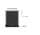
- Fig. 7A is a view for explaining detection processing in a shot region having a notch.
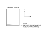
- Fig. 7B is a view for explaining detection processing in a shot region having a notch.
- Fig. 8 is view for explaining detection processing in a partial field.
- Fig. 9 is view for explaining detection processing in the partial field.
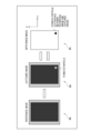
- Fig. 1 is a schematic view showing the arrangement of an imprint apparatus 100 according to an aspect of the present invention.
- the imprint apparatus 100 is a lithography apparatus which forms a pattern in an imprint material on a substrate using a mold.
- the imprint apparatus 100 performs an imprint process of forming the pattern on the substrate by curing the imprint material on the substrate in a state in which the mold and the imprint material are in contact with each other, and releasing the mold from the cured imprint material.
- an ultraviolet-curing resin material which is cured by irradiation with ultraviolet rays is used as the imprint material.
- the imprint material may be a thermoplastic resin material or a thermosetting resin material.
- the imprint apparatus 100 includes a mold stage 101 which moves while holding a mold 102, a substrate stage 104 which moves while holding a substrate 103, a light source 105 which emits the ultraviolet rays, and a resin supply unit 106 which supplies (applies) the ultraviolet-curing resin material onto the substrate.
- the imprint apparatus 100 also includes an off-axis alignment scope 107, a substrate chuck 108 which is arranged on the substrate stage and fixes the substrate 103, an image capturing unit 109, and on-axis alignment scopes 111.
- the imprint apparatus 100 further includes a reference plate 112 arranged on the substrate stage 104, a storage unit 113, and a processing unit 114.
- the image capturing unit 109 includes an image capturing light source 109a and an image sensor 109b.
- the image capturing unit 109 captures a shot region of the substrate 103 and obtains an image via the mold 102 or without going through the mold 102.
- the image capturing light source 109a illuminates the substrate 103 (shot region) with light having a wavelength different from those of the ultraviolet rays, that is, light (for example, visible light) having a wavelength different from the induced wavelength of a photo-curable resin material.
- the image sensor 109b includes, for example, a CCD image sensor or a CMOS image sensor, and detects light reflected by the pattern surface of the mold 102 and the surface of the substrate 103.
- the image sensor 109b also detects interference light between (an interference pattern formed by) light reflected by the mold 102 and light reflected by the substrate 103.
- the storage unit 113 includes, for example, a memory or a hard disk (HDD), and stores an image obtained by the image capturing unit 109 and a reference image used in detection processing to be described later.
- the storage unit 113 can also store various kinds of programs, data, information, and the like used in the imprint apparatus 100.
- the processing unit 114 includes, for example, a CPU and a memory and performs the imprint process by controlling the respective units of the imprint apparatus 100.
- the processing unit 114 also performs detection processing of detecting a foreign particle present between the mold 102 and the substrate 103.
- the foreign particle sandwiched between the mold 102 and the substrate 103 is detected when bringing the mold 102 and a resin material on the substrate 103 into contact with each other while performing the imprint process.
- the substrate 103 is caused to hold the substrate stage 104 in the imprint process.
- the off-axis alignment scope 107 detects a mark provided on the substrate 103 and a mark provided in the reference plate 112, thereby obtaining the position and shape shift amounts between the substrate 103 and the substrate stage 104.
- the on-axis alignment scopes 111 detect a mark provided in the mold 102 and the mark provided in the reference plate 112, thereby obtaining the position and shape shift amounts between the mold 102 and the substrate stage 104. Based on thus obtained position and shape shift amounts, position and shape shifts between the mold 102 and the substrate 103 are corrected (that is, alignment between the mold 102 and the substrate 103 is performed).
- each on-axis alignment scope 111 is a scope which detects the mark formed on the substrate 103 via the mold 102 and the off-axis alignment scope 107 is a scope which detects the mark formed on the substrate 103 without going through the mold 102.
- the resin supply unit 106 supplies a resin material to the shot region on the substrate 103. Then, the mold stage 101 which holds the mold 102 is moved to bring the mold 102 and the resin material on the substrate 103 (shot region) into contact with each other. After the concave portion of the pattern surface of the mold 102 is filled with the resin material, the light source 105 irradiates the resin material on the substrate 103 with the ultraviolet rays via the mold 102, thereby curing the resin material. Then, the mold stage 101 is moved to release the mold 102 from the cured resin on the substrate 103. As a result, the pattern of the resin material is formed on the substrate 103 (shot region).
- the image capturing unit 109 can capture a process in which the resin material on the substrate 103 fills the concave portion of the pattern surface while spreading between the mold 102 and the substrate 103.
- the image obtained by the image capturing unit 109 is thus stored in the storage unit 113, as described above.
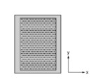
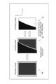
- Figs. 2A to 2F are views each schematically showing an image obtained by the image capturing unit 109 while performing the imprint process.
- Fig. 2A shows the image obtained by capturing the substrate 103 to which the resin material has been supplied from the resin supply unit 106 using the image capturing unit 109 in a state in which the substrate 103 is moved under the mold 102.
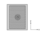
- Fig. 2B shows the image obtained by capturing the substrate 103 using the image capturing unit 109 in a state in which the mold 102 (the pattern surface thereof) is deformed into a convex shape on a substrate side, and a part (center portion) of the mold 102 and the resin material on the substrate 103 are in contact with each other.
- a gap is generated between the mold 102 and the substrate 103 by gradually contacting, with the resin material on the substrate 103, the mold 102 from its center portion to its peripheral portion, as described above.
- An interference pattern that is, Newton's ring pattern is observed, as shown in Fig. 2B.
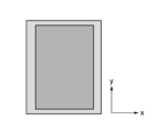
- Fig. 2C shows the image obtained by capturing the substrate 103 using the image capturing unit 109 in a state in which the mold 102 and the resin material on the substrate 103 are in contact with other in an entire region. In this state, however, the concave portion of the pattern surface of the mold 102 is not filled with the resin material, and thus bubbles are observed as shown in Fig. 2C.
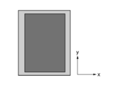
- Fig. 2D shows the image obtained by capturing the substrate 103 using the image capturing unit 109 in a state in which the concave portion of the pattern surface of the mold 102 is completely filled with the resin material, that is, in a state immediately before the light source 105 emits the ultraviolet rays. In this state, as shown in Fig. 2D, the Newton's rings and the bubbles as shown in Figs. 2B and 2C are not observed.
- Fig. 2E shows the image obtained by capturing the substrate 103 using the image capturing unit 109 in a state in which the light source 105 irradiates the resin material on the substrate 103 with the ultraviolet rays via the mold 102.
- Fig. 2F shows the image obtained by capturing the substrate 103 using the image capturing unit 109 in a state in which the mold 102 is released from the cured resin on the substrate 103.
- the abnormal array of the resin material to be a cause of the defect in the pattern, that is, the abnormal drop of the resin supply unit 106. More specifically, it is possible to detect the abnormal drop by comparing the image (the array of the droplets of the resin material) shown in Fig. 2A with the reference image (that is, the reference array of the resin material) obtained when the resin supply unit 106 supplies the droplets of the resin material normally. When such an abnormal drop is detected, it is effective, for reducing occurrence of the defect in the pattern, to supply the resin material onto the substrate 103 again by, for example, carrying out maintenance or exchange of the resin supply unit 106.
- each Newton's ring is not a perfect circle or the center of Newton's rings does not match that of the image. In this case, it is effective, for reducing occurrence of the defect in the pattern, to improve the parallelness between the mold 102 and the substrate 103 by, for example, correcting the tilt of the mold 102.
- the mold 102 is also possible, to be described later, to detect the foreign particle sandwiched between the mold 102 and the substrate 103 using the images shown in Figs. 2C and 2D.
- Such a sandwiched foreign particle not only causes the defect in the pattern formed on the substrate 103 but also damages the mold 102. Therefore, when the sandwiched foreign particle is detected, it is effective, for reducing occurrence of the defect in the pattern and damage to the mold, to cease the imprint process.
- the mold 102 is released from the resin material on the substrate 103 without curing the resin material.
- the substrate 103 may be processed by storing information on the shot region where the foreign particle has been detected (the position of the foreign particle), and then using stored information in a step after the imprint process. For example, the shot region where the foreign particle has been detected is stored as an error region.
- detection processing of detecting the foreign particle present between the mold 102 and the substrate 103 is particularly performed in order to reduce occurrence of the defect in the pattern formed on the substrate 103 and damage to the mold 102.
- detection processing is performed by comparing the image obtained by the image capturing unit 109 in a state in which the mold 102 and the resin material on the substrate 103 are in contact with each other while performing the imprint process, that is, the image shown in Fig. 2C or 2D with the reference image.
- the reference image is an image obtained in a state in which the mold 102 and the resin material on the substrate 103 are in contact with each other without sandwiching the foreign particle.
- a reference mark 3a shows a reference image.
- a reference mark 3b shows an image (captured image) obtained by the image capturing unit 109 in the state in which the mold 102 and the resin material on the substrate 103 are in contact with each other.
- the captured image shown in the reference mark 3b corresponds to the image shown in Fig. 2C or 2D and is an image obtained in a state in which a foreign particle is sandwiched between the mold 102 and the substrate 103.
- a reference mark 3c is a difference image showing the difference between the reference image shown in the reference mark 3a of Fig. 3 and the captured image shown in the reference mark 3b of Fig. 3. Referring to the reference mark 3c of Fig.
- the foreign particle sandwiched between the mold 102 and the substrate 103 is extracted as the difference (black dot) between the reference image and the captured image. As described above, it is possible to detect the foreign particle present between the mold 102 and the substrate 103 by comparing the reference image with the captured image.
- the image (captured image) captured by the image capturing unit 109 in the state in which the mold 102 and the resin material on the substrate 103 are in contact with each other while performing the imprint process has been described here as the image shown in Fig. 2C or 2D.
- the image obtained in a state in which the concave portion of the pattern surface of the mold 102 is not filled with the resin material, that is, the image shown in Fig. 2C includes the bubbles as described above. Therefore, when the difference between the reference image and the image shown in Fig. 2C is calculated, the bubbles may be extracted and erroneously detected as foreign particles.
- the image obtained in the state in which the concave portion of the pattern surface of the mold 102 is filled with the resin material that is, the image shown in Fig. 2D can be compared with the reference image.
- the image obtained in the state in which the concave portion of the pattern surface of the mold 102 is filled with the resin material has a small change caused by a factor other than the foreign particle and can detect the foreign particle most stably in detection processing. Note that in general, it takes about two to three sec until the concave portion of the pattern surface of the mold 102 is filled with the resin material on the substrate 103 after bringing the mold 102 and the resin material into contact with each other.
- the image capturing unit 109 can be caused to obtain the image after a lapse of a predetermined time (for example, two to three sec) from time when the mold 102 and the resin material on the substrate 103 are brought into contact with each other.
- a predetermined time for example, two to three sec
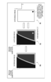
- Detection processing has been described above when the captured image obtained by the image capturing unit 109 indicates not a peripheral shot region (edge shot) having the periphery of the substrate 103 but a shot region inside the peripheral shot region.
- the captured image includes a region outside of the substrate 103 as shown in a reference mark 4b of Fig. 4.
- the peripheral shot region will be referred to as a partial field and the shot region inside the peripheral shot region will be referred to as a full field, hereinafter.
- the region outside the substrate is extracted and erroneously detected as a foreign particle as shown in a reference mark 4c of Fig. 4.
- the region outside the substrate is excluded from a target of detection processing. It is possible to specify, based on the distance between the center position of the substrate 103 and a position on the substrate 103 corresponding to the center of the captured image obtained by the image capturing unit 109, whether the captured image includes the region outside the substrate.
- the substrate 103 basically has a circular shape. It is therefore possible to prevent a region outside of a radius R (region outside the substrate) from the center position of the substrate 103 from being erroneously detected as a foreign particle by excluding the region outside the substrate from the target of detection processing as shown in Fig. 5. More specifically, let the region outside the substrate be the region outside of the radius R relative to the center position of the substrate 103. For example, letting (X, Y) be the center coordinates of the shot region relative to the center position of the substrate 103 and (x, y) be respective coordinates from the center coordinates of the shot region, a region on a condition given by: is excluded from the target of detection processing as the region outside the substrate. In Fig. 5, a region shown in gray becomes a region excluded from the target of detection processing.
- a reference mark 6a of Fig. 6 shows a reference image corresponding to the full field.
- a reference mark 6b of Fig. 6 shows an image (captured image) obtained by the image capturing unit 109 in the state in which the mold 102 and the resin material on the substrate 103 are in contact with each other.
- the captured image shown in the reference mark 6b of Fig. 6 is an image obtained in a state in which a foreign particle is sandwiched between the mold 102 and the substrate 103 in the partial field.
- a reference mark 6c of Fig. 6 is a difference image showing the difference between the reference image shown in the reference mark 6a of Fig. 6 and the captured image shown in the reference mark 6b of Fig. 6.
- the foreign particle sandwiched between the mold 102 and the substrate 103 is extracted as the difference (black dot) between the reference image and the captured image. It is possible, however, to correctly detect only the foreign particle present between the mold 102 and the substrate 103 without detecting a region outside the substrate (region shown in gray) as a foreign particle because the region outside the substrate has been excluded from the target of detection processing.
- data regarding the region outside the substrate in the captured image may be deleted before obtaining the difference image by comparing the reference image with the captured image or data regarding the region outside the substrate in the difference image may be ignored after obtaining the difference image.
- the captured image When a captured image obtained by the image capturing unit 109 is a shot region having a notch, the captured image has the notch as shown in Fig. 7A.
- the notch When comparing the captured image corresponding to the shot region having the notch as shown in Fig. 7A with the reference image (the reference mark 6a of Fig. 6) corresponding to the full field, the notch is erroneously detected as a foreign particle like the region outside the substrate.
- the notch is a cut indicating the crystal orientation of a silicon wafer.
- Fig. 7B is a difference image showing the difference between the reference image (the reference mark 6a of Fig. 6) and the captured image shown in Fig. 7A. Referring to Fig. 7B, it is possible to correctly detect only the foreign particle present between the mold 102 and the substrate 103 without detecting the region where the notch has been formed (region shown in gray) as the foreign particle because the region has been excluded from the target of detection processing.
- the region where the notch has been formed is preferably excluded from detection processing even if the region is a region inside the substrate (region inside of the radius R). This also applies to a region where an orientation flat has been formed on the substrate.
- the processing unit 114 is caused to function as a setting unit which sets a region on the substrate in accordance with a user input and the region is excluded from the target of detection processing.
- the imprint apparatus 100 of this embodiment detects the foreign particle present between the mold 102 and the substrate 103 while performing the imprint process. Therefore, the imprint apparatus 100 can reduce occurrence of the defect in the pattern formed on the substrate 103 and damage to the mold 102. In this embodiment, it is also possible detect, by excluding the region outside the substrate 103 from the target of detection processing, the foreign particle present between the mold 102 and the substrate 103 using the reference image corresponding to the full field even if the captured image is the partial field.
- a storage unit 113 stores a reference image corresponding to each shot region of a substrate 103.
- a processing unit 114 selects a reference image corresponding to the shot region of the captured image from the plurality of reference images stored in the storage unit 113 when performing detection processing of detecting a foreign particle present between a mold 102 and the substrate 103. Then, the processing unit 114 detects the foreign particle present between the mold 102 and the substrate 103 by comparing the captured image with the selected reference image, as in the first embodiment.
- the storage unit 113 may store not the reference images with respect to all the shot regions of the substrate 103 but the first reference image corresponding to each partial field and the second reference image corresponding to at least one full field.
- the captured image is the partial field
- the foreign particle present between the mold 102 and the substrate 103 is detected by comparing the captured image with the first reference image corresponding to the partial field.
- the captured image is the full field
- the foreign particle present between the mold 102 and the substrate 103 is detected by comparing the captured image with the second reference image.
- a reference mark 8a of Fig. 8 shows the reference image corresponding to the partial field.
- a reference mark 8b of Fig. 8 shows the image (captured image) obtained by the image capturing unit 109 in a state in which the mold 102 and a resin on the substrate 103 are in contact with each other.
- the captured image shown in the reference mark 8b of Fig. 8 is an image obtained in a state in which a foreign particle is sandwiched between the mold 102 and the substrate 103 in the partial field.
- the foreign particle sandwiched between the mold 102 and the substrate 103 is extracted as the difference (black dot) between the reference image and the captured image. It is possible to correctly detect only the foreign particle present between the mold 102 and the substrate 103 without detecting a region outside the substrate 103 as a foreign particle because the reference image corresponds to the partial field.
- the state of an imprint apparatus 100 and more specifically, the state of a region outside of a substrate chuck 108 (the region outside the substrate) arranged on a substrate stage 104 may be different between times when the reference image is obtained and when the captured image is obtained.
- this embodiment and the first embodiment can be combined as shown in Fig. 9.
- a reference mark 9a of Fig. 9 shows a reference image corresponding to the partial field.
- a reference mark 9b of Fig. 9 shows an image (captured image) obtained by the image capturing unit 109 in the state in which the mold 102 and the resin on the substrate 103 are in contact with each other.
- a reference mark 9c of Fig. 9 is a difference image showing the difference between the reference image shown in the reference mark 9a of Fig. 9 and the captured image shown in the reference mark 9b of Fig. 9. Referring to the reference mark 9c of Fig. 9, the foreign particle sandwiched between the mold 102 and the substrate 103 is extracted as the difference (black dot) between the reference image and the captured image.
- the manufacturing method includes a step of forming a pattern on a substrate (a wafer, a glass plate, a film-like substrate, or the like) using an imprint apparatus 100.
- the manufacturing method further includes a step of processing the substrate on which the pattern has been formed.
- the processing step can include a step of removing the residual film of the pattern.
- the processing step can also include another known step such as a step of etching the substrate using the pattern as a mask.
- the method of manufacturing the article according to this embodiment is advantageous in at least one of the performance, the quality, the productivity, and the production cost of the article, as compared to conventional methods.
Landscapes
- Engineering & Computer Science (AREA)
- Mechanical Engineering (AREA)
- Physics & Mathematics (AREA)
- General Physics & Mathematics (AREA)
- Shaping Of Tube Ends By Bending Or Straightening (AREA)
- Exposure Of Semiconductors, Excluding Electron Or Ion Beam Exposure (AREA)
- Investigating Materials By The Use Of Optical Means Adapted For Particular Applications (AREA)
Priority Applications (4)
| Application Number | Priority Date | Filing Date | Title |
|---|---|---|---|
| US15/546,857 US10751930B2 (en) | 2015-04-14 | 2016-03-07 | Imprint apparatus, imprint method, and method of manufacturing article |
| CN201680021127.9A CN107430988B (zh) | 2015-04-14 | 2016-03-07 | 压印装置、压印方法和制造物品的方法 |
| SG11201707268PA SG11201707268PA (en) | 2015-04-14 | 2016-03-07 | Imprint apparatus, imprint method, and method of manufacturing article |
| KR1020177032065A KR101974771B1 (ko) | 2015-04-14 | 2016-03-07 | 임프린트 장치, 임프린트 방법 및 물품의 제조 방법 |
Applications Claiming Priority (2)
| Application Number | Priority Date | Filing Date | Title |
|---|---|---|---|
| JP2015-082856 | 2015-04-14 | ||
| JP2015082856A JP6403627B2 (ja) | 2015-04-14 | 2015-04-14 | インプリント装置、インプリント方法及び物品の製造方法 |
Publications (1)
| Publication Number | Publication Date |
|---|---|
| WO2016166929A1 true WO2016166929A1 (en) | 2016-10-20 |
Family
ID=57126743
Family Applications (1)
| Application Number | Title | Priority Date | Filing Date |
|---|---|---|---|
| PCT/JP2016/001218 WO2016166929A1 (en) | 2015-04-14 | 2016-03-07 | Imprint apparatus, imprint method, and method of manufacturing article |
Country Status (7)
Cited By (2)
| Publication number | Priority date | Publication date | Assignee | Title |
|---|---|---|---|---|
| US11030738B2 (en) | 2019-07-05 | 2021-06-08 | International Business Machines Corporation | Image defect identification |
| US11295439B2 (en) | 2019-10-16 | 2022-04-05 | International Business Machines Corporation | Image recovery |
Families Citing this family (10)
| Publication number | Priority date | Publication date | Assignee | Title |
|---|---|---|---|---|
| JP6799397B2 (ja) * | 2015-08-10 | 2020-12-16 | キヤノン株式会社 | インプリント装置、および物品の製造方法 |
| JP6541518B2 (ja) * | 2015-09-04 | 2019-07-10 | キヤノン株式会社 | インプリント装置、インプリント方法、および物品の製造方法 |
| JP6971599B2 (ja) * | 2017-03-15 | 2021-11-24 | キヤノン株式会社 | インプリント装置、欠陥検査方法、パターン形成方法および物品製造方法 |
| JP2017120930A (ja) * | 2017-03-28 | 2017-07-06 | 大日本印刷株式会社 | インプリント装置及びインプリント方法 |
| JP7241493B2 (ja) * | 2017-11-07 | 2023-03-17 | キヤノン株式会社 | インプリント装置、情報処理装置、及び物品の製造方法 |
| JP7328109B2 (ja) * | 2019-10-02 | 2023-08-16 | キヤノン株式会社 | 型、平坦化装置、平坦化方法及び物品の製造方法 |
| JP7391806B2 (ja) * | 2020-09-16 | 2023-12-05 | キオクシア株式会社 | インプリント装置、情報処理装置、及びインプリント方法 |
| JP7685941B2 (ja) * | 2021-04-14 | 2025-05-30 | キヤノン株式会社 | インプリント装置、インプリント方法及び物品の製造方法 |
| US12353127B2 (en) | 2021-04-14 | 2025-07-08 | Canon Kabushiki Kaisha | Imprint apparatus, imprint method and article manufacturing method |
| JP7721736B1 (ja) * | 2024-05-14 | 2025-08-12 | キヤノン株式会社 | 平坦化装置、平坦化方法、および物品の製造方法 |
Citations (6)
| Publication number | Priority date | Publication date | Assignee | Title |
|---|---|---|---|---|
| US20090261504A1 (en) * | 2008-04-22 | 2009-10-22 | Fuji Electric Device Technology Co., Ltd. | Imprinting method and apparatus therefor |
| JP2010149469A (ja) * | 2008-12-26 | 2010-07-08 | Showa Denko Kk | インプリント装置およびモールドの汚染検出方法 |
| JP2011240662A (ja) * | 2010-05-20 | 2011-12-01 | Toshiba Corp | インプリント方法、インプリント装置及びプログラム |
| JP2015018997A (ja) * | 2013-07-12 | 2015-01-29 | 大日本印刷株式会社 | インプリント装置及びインプリント方法 |
| JP2015050217A (ja) * | 2013-08-30 | 2015-03-16 | 大日本印刷株式会社 | インプリント方法およびインプリント装置 |
| US20150076724A1 (en) * | 2013-09-13 | 2015-03-19 | Canon Kabushiki Kaisha | Imprint apparatus, imprint method, detecting method, and method of manufacturing device |
Family Cites Families (10)
| Publication number | Priority date | Publication date | Assignee | Title |
|---|---|---|---|---|
| US20080160129A1 (en) | 2006-05-11 | 2008-07-03 | Molecular Imprints, Inc. | Template Having a Varying Thickness to Facilitate Expelling a Gas Positioned Between a Substrate and the Template |
| JP2005214980A (ja) * | 2005-01-31 | 2005-08-11 | Miyazaki Oki Electric Co Ltd | ウエハのマクロ検査方法および自動ウエハマクロ検査装置 |
| JP2006294684A (ja) * | 2005-04-06 | 2006-10-26 | Nikon Corp | 表面検査装置 |
| US8945444B2 (en) | 2007-12-04 | 2015-02-03 | Canon Nanotechnologies, Inc. | High throughput imprint based on contact line motion tracking control |
| JP2010203892A (ja) * | 2009-03-03 | 2010-09-16 | Nikon Corp | 基板検査方法 |
| JP5173944B2 (ja) * | 2009-06-16 | 2013-04-03 | キヤノン株式会社 | インプリント装置及び物品の製造方法 |
| JP5455583B2 (ja) * | 2009-11-30 | 2014-03-26 | キヤノン株式会社 | インプリント装置 |
| KR101414830B1 (ko) | 2011-11-30 | 2014-07-03 | 다이닛뽕스크린 세이조오 가부시키가이샤 | 얼라이먼트 방법, 전사 방법 및 전사장치 |
| JP5960198B2 (ja) | 2013-07-02 | 2016-08-02 | キヤノン株式会社 | パターン形成方法、リソグラフィ装置、リソグラフィシステムおよび物品製造方法 |
| JP6230353B2 (ja) | 2013-09-25 | 2017-11-15 | キヤノン株式会社 | パターン形状を有する膜の製造方法、光学部品の製造方法、回路基板の製造方法、電子機器の製造方法 |
-
2015
- 2015-04-14 JP JP2015082856A patent/JP6403627B2/ja active Active
-
2016
- 2016-03-07 SG SG11201707268PA patent/SG11201707268PA/en unknown
- 2016-03-07 KR KR1020177032065A patent/KR101974771B1/ko active Active
- 2016-03-07 WO PCT/JP2016/001218 patent/WO2016166929A1/en active Application Filing
- 2016-03-07 US US15/546,857 patent/US10751930B2/en active Active
- 2016-03-07 CN CN201680021127.9A patent/CN107430988B/zh active Active
- 2016-03-16 TW TW105108097A patent/TWI655076B/zh active
Patent Citations (6)
| Publication number | Priority date | Publication date | Assignee | Title |
|---|---|---|---|---|
| US20090261504A1 (en) * | 2008-04-22 | 2009-10-22 | Fuji Electric Device Technology Co., Ltd. | Imprinting method and apparatus therefor |
| JP2010149469A (ja) * | 2008-12-26 | 2010-07-08 | Showa Denko Kk | インプリント装置およびモールドの汚染検出方法 |
| JP2011240662A (ja) * | 2010-05-20 | 2011-12-01 | Toshiba Corp | インプリント方法、インプリント装置及びプログラム |
| JP2015018997A (ja) * | 2013-07-12 | 2015-01-29 | 大日本印刷株式会社 | インプリント装置及びインプリント方法 |
| JP2015050217A (ja) * | 2013-08-30 | 2015-03-16 | 大日本印刷株式会社 | インプリント方法およびインプリント装置 |
| US20150076724A1 (en) * | 2013-09-13 | 2015-03-19 | Canon Kabushiki Kaisha | Imprint apparatus, imprint method, detecting method, and method of manufacturing device |
Cited By (2)
| Publication number | Priority date | Publication date | Assignee | Title |
|---|---|---|---|---|
| US11030738B2 (en) | 2019-07-05 | 2021-06-08 | International Business Machines Corporation | Image defect identification |
| US11295439B2 (en) | 2019-10-16 | 2022-04-05 | International Business Machines Corporation | Image recovery |
Also Published As
| Publication number | Publication date |
|---|---|
| US20180022015A1 (en) | 2018-01-25 |
| SG11201707268PA (en) | 2017-10-30 |
| TW201636186A (zh) | 2016-10-16 |
| CN107430988A (zh) | 2017-12-01 |
| TWI655076B (zh) | 2019-04-01 |
| US10751930B2 (en) | 2020-08-25 |
| KR101974771B1 (ko) | 2019-05-02 |
| CN107430988B (zh) | 2020-07-10 |
| KR20170133501A (ko) | 2017-12-05 |
| JP6403627B2 (ja) | 2018-10-10 |
| JP2016201522A (ja) | 2016-12-01 |
Similar Documents
| Publication | Publication Date | Title |
|---|---|---|
| US10751930B2 (en) | Imprint apparatus, imprint method, and method of manufacturing article | |
| JP6931408B2 (ja) | 未硬化の材料を硬化させる装置、未硬化の材料が吐出されているか否かを判定する方法及び未硬化の材料を硬化させる物品の製造方法 | |
| US9387607B2 (en) | Imprint apparatus, imprint method, and method for producing device | |
| TWI392578B (zh) | 即時壓印程序缺陷診斷技術 | |
| US20210114284A1 (en) | Imprint method and template | |
| US10754264B2 (en) | Lithography apparatus, lithography method, decision method, storage medium, and article manufacturing method | |
| JP6413533B2 (ja) | 物品の品質判別方法、物品の品質判別システムおよび物品の製造方法 | |
| KR20200107804A (ko) | 임프린트 장치의 제어 방법, 임프린트 장치, 및 물품 제조방법 | |
| KR102172881B1 (ko) | 임프린트 장치 및 물품 제조 방법 | |
| US11681216B2 (en) | Imprint apparatus, imprint method, article manufacturing method, molding apparatus, and molding method | |
| CN105759566B (zh) | 压印装置、压印方法以及物品的制造方法 | |
| JP6643022B2 (ja) | インプリント装置、インプリント方法、異物検出方法および物品製造方法 | |
| JP2018156986A (ja) | インプリント装置、欠陥検査方法、パターン形成方法および物品製造方法 | |
| JP6685715B2 (ja) | 位置検出方法、プログラム、位置検出装置、リソグラフィ装置、および物品の製造方法 | |
| JP7043199B2 (ja) | インプリント方法、プログラム、インプリント装置及び物品の製造方法 | |
| JP2023020870A (ja) | 情報処理装置、成形装置、成形方法及び物品の製造方法 | |
| US20240377767A1 (en) | Imprint apparatus, imprint method, and article manufacturing method | |
| US12194671B2 (en) | Information processing apparatus, molding apparatus, molding method, and article manufacturing method | |
| US20250076213A1 (en) | Foreign substance inspection method, foreign substance inspection apparatus, molding method, molding apparatus, and article manufacturing method | |
| JP2016207816A (ja) | インプリント装置、インプリント方法および物品製造方法 |
Legal Events
| Date | Code | Title | Description |
|---|---|---|---|
| 121 | Ep: the epo has been informed by wipo that ep was designated in this application |
Ref document number: 16779728 Country of ref document: EP Kind code of ref document: A1 |
|
| WWE | Wipo information: entry into national phase |
Ref document number: 15546857 Country of ref document: US |
|
| WWE | Wipo information: entry into national phase |
Ref document number: 11201707268P Country of ref document: SG |
|
| NENP | Non-entry into the national phase |
Ref country code: DE |
|
| ENP | Entry into the national phase |
Ref document number: 20177032065 Country of ref document: KR Kind code of ref document: A |
|
| 122 | Ep: pct application non-entry in european phase |
Ref document number: 16779728 Country of ref document: EP Kind code of ref document: A1 |