JP6541518B2 - インプリント装置、インプリント方法、および物品の製造方法 - Google Patents
インプリント装置、インプリント方法、および物品の製造方法 Download PDFInfo
- Publication number
- JP6541518B2 JP6541518B2 JP2015174407A JP2015174407A JP6541518B2 JP 6541518 B2 JP6541518 B2 JP 6541518B2 JP 2015174407 A JP2015174407 A JP 2015174407A JP 2015174407 A JP2015174407 A JP 2015174407A JP 6541518 B2 JP6541518 B2 JP 6541518B2
- Authority
- JP
- Japan
- Prior art keywords
- mold
- imprint
- substrate
- unit
- imaging
- Prior art date
- Legal status (The legal status is an assumption and is not a legal conclusion. Google has not performed a legal analysis and makes no representation as to the accuracy of the status listed.)
- Active
Links
Images

Classifications
-
- G—PHYSICS
- G03—PHOTOGRAPHY; CINEMATOGRAPHY; ANALOGOUS TECHNIQUES USING WAVES OTHER THAN OPTICAL WAVES; ELECTROGRAPHY; HOLOGRAPHY
- G03F—PHOTOMECHANICAL PRODUCTION OF TEXTURED OR PATTERNED SURFACES, e.g. FOR PRINTING, FOR PROCESSING OF SEMICONDUCTOR DEVICES; MATERIALS THEREFOR; ORIGINALS THEREFOR; APPARATUS SPECIALLY ADAPTED THEREFOR
- G03F7/00—Photomechanical, e.g. photolithographic, production of textured or patterned surfaces, e.g. printing surfaces; Materials therefor, e.g. comprising photoresists; Apparatus specially adapted therefor
- G03F7/70—Microphotolithographic exposure; Apparatus therefor
- G03F7/70216—Mask projection systems
- G03F7/7035—Proximity or contact printers
-
- G—PHYSICS
- G03—PHOTOGRAPHY; CINEMATOGRAPHY; ANALOGOUS TECHNIQUES USING WAVES OTHER THAN OPTICAL WAVES; ELECTROGRAPHY; HOLOGRAPHY
- G03F—PHOTOMECHANICAL PRODUCTION OF TEXTURED OR PATTERNED SURFACES, e.g. FOR PRINTING, FOR PROCESSING OF SEMICONDUCTOR DEVICES; MATERIALS THEREFOR; ORIGINALS THEREFOR; APPARATUS SPECIALLY ADAPTED THEREFOR
- G03F7/00—Photomechanical, e.g. photolithographic, production of textured or patterned surfaces, e.g. printing surfaces; Materials therefor, e.g. comprising photoresists; Apparatus specially adapted therefor
- G03F7/0002—Lithographic processes using patterning methods other than those involving the exposure to radiation, e.g. by stamping
-
- G—PHYSICS
- G03—PHOTOGRAPHY; CINEMATOGRAPHY; ANALOGOUS TECHNIQUES USING WAVES OTHER THAN OPTICAL WAVES; ELECTROGRAPHY; HOLOGRAPHY
- G03F—PHOTOMECHANICAL PRODUCTION OF TEXTURED OR PATTERNED SURFACES, e.g. FOR PRINTING, FOR PROCESSING OF SEMICONDUCTOR DEVICES; MATERIALS THEREFOR; ORIGINALS THEREFOR; APPARATUS SPECIALLY ADAPTED THEREFOR
- G03F7/00—Photomechanical, e.g. photolithographic, production of textured or patterned surfaces, e.g. printing surfaces; Materials therefor, e.g. comprising photoresists; Apparatus specially adapted therefor
- G03F7/70—Microphotolithographic exposure; Apparatus therefor
- G03F7/70483—Information management; Active and passive control; Testing; Wafer monitoring, e.g. pattern monitoring
- G03F7/70491—Information management, e.g. software; Active and passive control, e.g. details of controlling exposure processes or exposure tool monitoring processes
- G03F7/70525—Controlling normal operating mode, e.g. matching different apparatus, remote control or prediction of failure
-
- G—PHYSICS
- G03—PHOTOGRAPHY; CINEMATOGRAPHY; ANALOGOUS TECHNIQUES USING WAVES OTHER THAN OPTICAL WAVES; ELECTROGRAPHY; HOLOGRAPHY
- G03F—PHOTOMECHANICAL PRODUCTION OF TEXTURED OR PATTERNED SURFACES, e.g. FOR PRINTING, FOR PROCESSING OF SEMICONDUCTOR DEVICES; MATERIALS THEREFOR; ORIGINALS THEREFOR; APPARATUS SPECIALLY ADAPTED THEREFOR
- G03F7/00—Photomechanical, e.g. photolithographic, production of textured or patterned surfaces, e.g. printing surfaces; Materials therefor, e.g. comprising photoresists; Apparatus specially adapted therefor
- G03F7/70—Microphotolithographic exposure; Apparatus therefor
- G03F7/70483—Information management; Active and passive control; Testing; Wafer monitoring, e.g. pattern monitoring
- G03F7/70605—Workpiece metrology
- G03F7/70616—Monitoring the printed patterns
- G03F7/7065—Defects, e.g. optical inspection of patterned layer for defects
-
- G—PHYSICS
- G03—PHOTOGRAPHY; CINEMATOGRAPHY; ANALOGOUS TECHNIQUES USING WAVES OTHER THAN OPTICAL WAVES; ELECTROGRAPHY; HOLOGRAPHY
- G03F—PHOTOMECHANICAL PRODUCTION OF TEXTURED OR PATTERNED SURFACES, e.g. FOR PRINTING, FOR PROCESSING OF SEMICONDUCTOR DEVICES; MATERIALS THEREFOR; ORIGINALS THEREFOR; APPARATUS SPECIALLY ADAPTED THEREFOR
- G03F7/00—Photomechanical, e.g. photolithographic, production of textured or patterned surfaces, e.g. printing surfaces; Materials therefor, e.g. comprising photoresists; Apparatus specially adapted therefor
- G03F7/70—Microphotolithographic exposure; Apparatus therefor
- G03F7/708—Construction of apparatus, e.g. environment aspects, hygiene aspects or materials
- G03F7/70908—Hygiene, e.g. preventing apparatus pollution, mitigating effect of pollution or removing pollutants from apparatus
- G03F7/70925—Cleaning, i.e. actively freeing apparatus from pollutants, e.g. using plasma cleaning
Landscapes
- Physics & Mathematics (AREA)
- General Physics & Mathematics (AREA)
- Engineering & Computer Science (AREA)
- Health & Medical Sciences (AREA)
- Epidemiology (AREA)
- Public Health (AREA)
- Plasma & Fusion (AREA)
- Life Sciences & Earth Sciences (AREA)
- Atmospheric Sciences (AREA)
- Environmental & Geological Engineering (AREA)
- Shaping Of Tube Ends By Bending Or Straightening (AREA)
- Exposure Of Semiconductors, Excluding Electron Or Ion Beam Exposure (AREA)
Description
(装置構成)
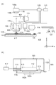
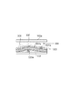
図1(a)は本実施形態のインプリント装置100の構成を示す図である。図1において、光源101から出射され、モールド102を透過して基板103に入射する紫外線104の光の光軸に平行な軸をZ軸(本実施形態では鉛直方向)とする。Z軸に垂直な平面内において直交する2軸をX軸、Y軸とする。
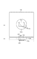
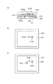
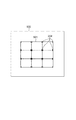
インプリント装置100は、パターン部102aと樹脂114とが接触している状態で取得される画像(第1撮像結果)と、硬化した樹脂114からパターン部102aを引き離した状態で取得される画像(第2撮像結果)とを比較して、異物を検出する。
前述のように、離型前の撮像工程は樹脂114を硬化させた後の方が好ましい。硬化する前後における樹脂114の光学特性の変化によって、撮像素子119bに入射する光の強度が変化する場合であっても、離型前後の画像の異物501a、502a、503aのない領域における画素値を一定にできる。よって画像504と画像505を比較しやすくなる。
本発明の実施形態にかかる物品の製造方法は、インプリント装置を用いて基板(ウエハやガラス板等)上にパターンを形成する工程と、パターンの形成露光された基板に対して加工処理を施す工程とを含む。物品とは、例えば、半導体集積回路素子、液晶表示素子、撮像素子、磁気ヘッド、CD−RW、光学素子、フォトマスク等である。加工処理とは、例えば、エッチング処理、あるいはイオン注入処理である。さらに、他の周知の処理工程(現像、酸化、成膜、蒸着、平坦化、インプリント材剥離、ダイシング、ボンディング、パッケージング等)を含んでも良い。
102 モールド
103 基板
105 移動体
106 基板保持部(載置部)
114 樹脂(インプリント材)
119 撮像ユニット
119b 撮像素子(撮像手段)
503a 異物(載置部と基板との間の異物)
120 制御部(検知手段、算出手段)
Claims (11)
- モールドを用いて基板上にインプリント材のパターンを形成するインプリント装置であって、
前記基板が載置される載置部と、
前記インプリント材を撮像する撮像手段と、
前記載置部と前記基板との間の異物を検知する検知手段とを有し、
前記検知手段は、前記モールドと接触させた前記インプリント材と前記モールドとを引き離す前における前記撮像手段の第1撮像結果及び、前記モールドと接触させた前記インプリント材と前記モールドとを引き離した後における前記撮像手段の第2撮像結果に基づいて、前記異物を検知すること特徴とするインプリント装置。 - 前記撮像手段は、前記モールドを透過させた光を用いて前記インプリント材を撮像することを特徴とする請求項1に記載のインプリント装置。
- 前記検知手段は、前記第1撮像結果である画像の画素情報と、前記第2撮像結果である画像の画素情報との差に基づいて前記異物を検知することを特徴とする請求項1又は2に記載のインプリント装置。
- 前記第2撮像結果を用いて、前記検知手段により検知された異物の位置および大きさのうち少なくとも一方の情報を算出する算出手段を有することを特徴とする請求項1乃至3のいずれか1項に記載のインプリント装置。
- 前記算出手段は、撮像視野に対する前記モールドのパターン形成部の位置に基づいて前記載置部を載せて移動する移動体に対する前記異物の位置を取得することを特徴とする請求項4に記載のインプリント装置。
- 前記載置部をクリーニングするクリーニングユニットをさらに有し、
前記クリーニングユニットは、前記検知手段が前記異物を検知した場合に、前記載置部をクリーニングすることを特徴とする請求項1乃至5のいずれか1項に記載のインプリント装置。 - 前記引き離す前とは、前記インプリント材と前記モールドとを接触させた後かつ前記インプリント材と前記モールドとを引き離す動作の開始前であり、前記引き離した後とは、前記引き離す動作の完了後であることを特徴とする請求項1乃至6のいずれか1項に記載のインプリント装置。
- 前記引き離す前とは、前記インプリント材を硬化させた後かつ前記引き離し動作の開始前であることを特徴とする請求項1乃至7のいずれか1項に記載のインプリント装置。
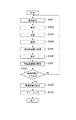
- モールドを用いて基板上にインプリント材のパターンを形成するインプリント方法であって、
前記インプリント材と前記モールドとを接触させる接触工程と、
前記接触工程の後に前記インプリント材と前記モールドとを引き離す工程である引き離し工程と、
前記接触工程の後かつ前記引き離し工程の前に撮像された前記インプリント材の雑像結果と、前記引き離し工程の後に撮像された前記インプリント材の撮像結果に基づいて、前記基板が載置される載置部と前記基板との間の異物を検知する検知工程と、を有することを特徴とするインプリント方法。 - 前記検知工程において前記異物を検知した場合に、前記載置部および前記基板の少なくとも一方をクリーニングする工程を有することを特徴とする請求項9に記載のインプリント方法。
- 請求項1乃至8のいずれか1項に記載のインプリント装置を用いて基板上に樹脂のパターンを形成する工程と、
前記工程で前記パターンを形成された基板を加工する工程と、を含むことを特徴とする物品の製造方法。
Priority Applications (3)
| Application Number | Priority Date | Filing Date | Title |
|---|---|---|---|
| JP2015174407A JP6541518B2 (ja) | 2015-09-04 | 2015-09-04 | インプリント装置、インプリント方法、および物品の製造方法 |
| KR1020187008576A KR101980497B1 (ko) | 2015-09-04 | 2016-08-03 | 임프린트 장치, 임프린트 방법 및 물품의 제조 방법 |
| PCT/JP2016/003579 WO2017038007A1 (en) | 2015-09-04 | 2016-08-03 | Imprint apparatus, imprint method, and method of manufacturing article |
Applications Claiming Priority (1)
| Application Number | Priority Date | Filing Date | Title |
|---|---|---|---|
| JP2015174407A JP6541518B2 (ja) | 2015-09-04 | 2015-09-04 | インプリント装置、インプリント方法、および物品の製造方法 |
Publications (3)
| Publication Number | Publication Date |
|---|---|
| JP2017050482A JP2017050482A (ja) | 2017-03-09 |
| JP2017050482A5 JP2017050482A5 (ja) | 2018-09-13 |
| JP6541518B2 true JP6541518B2 (ja) | 2019-07-10 |
Family
ID=58186870
Family Applications (1)
| Application Number | Title | Priority Date | Filing Date |
|---|---|---|---|
| JP2015174407A Active JP6541518B2 (ja) | 2015-09-04 | 2015-09-04 | インプリント装置、インプリント方法、および物品の製造方法 |
Country Status (3)
| Country | Link |
|---|---|
| JP (1) | JP6541518B2 (ja) |
| KR (1) | KR101980497B1 (ja) |
| WO (1) | WO2017038007A1 (ja) |
Cited By (2)
| Publication number | Priority date | Publication date | Assignee | Title |
|---|---|---|---|---|
| EP4534985A1 (en) | 2023-08-31 | 2025-04-09 | Canon Kabushiki Kaisha | Foreign substance inspection method, foreign substance inspection apparatus, molding method, molding apparatus, and article manufacturing method |
| WO2025258477A1 (ja) * | 2024-06-11 | 2025-12-18 | キヤノン株式会社 | 基板処理システムおよび基板処理方法 |
Families Citing this family (3)
| Publication number | Priority date | Publication date | Assignee | Title |
|---|---|---|---|---|
| JP6887279B2 (ja) * | 2017-03-24 | 2021-06-16 | キヤノン株式会社 | インプリント装置および物品製造方法 |
| JP7043199B2 (ja) * | 2017-08-03 | 2022-03-29 | キヤノン株式会社 | インプリント方法、プログラム、インプリント装置及び物品の製造方法 |
| JP7721736B1 (ja) | 2024-05-14 | 2025-08-12 | キヤノン株式会社 | 平坦化装置、平坦化方法、および物品の製造方法 |
Family Cites Families (13)
| Publication number | Priority date | Publication date | Assignee | Title |
|---|---|---|---|---|
| JPH1070069A (ja) * | 1996-08-28 | 1998-03-10 | Canon Inc | 半導体露光装置におけるごみ検出装置 |
| JP4994273B2 (ja) * | 2008-03-05 | 2012-08-08 | 株式会社日立ハイテクノロジーズ | プロキシミティ露光装置、プロキシミティ露光装置の基板移動方法、及び表示用パネル基板の製造方法 |
| JP2010149469A (ja) * | 2008-12-26 | 2010-07-08 | Showa Denko Kk | インプリント装置およびモールドの汚染検出方法 |
| JP5173944B2 (ja) * | 2009-06-16 | 2013-04-03 | キヤノン株式会社 | インプリント装置及び物品の製造方法 |
| US11133118B2 (en) * | 2012-05-22 | 2021-09-28 | University Of Massachusetts | Patterned nanoparticle structures |
| JP2014103385A (ja) * | 2012-10-26 | 2014-06-05 | Canon Inc | 検出装置、リソグラフィ装置、物品の製造方法及び検出方法 |
| JP6331292B2 (ja) * | 2013-08-30 | 2018-05-30 | 大日本印刷株式会社 | インプリント方法およびインプリント装置 |
| JP6282069B2 (ja) * | 2013-09-13 | 2018-02-21 | キヤノン株式会社 | インプリント装置、インプリント方法、検出方法及びデバイス製造方法 |
| JP6313585B2 (ja) * | 2013-12-10 | 2018-04-18 | キヤノン株式会社 | 露光装置及び物品の製造方法 |
| JP2016025230A (ja) * | 2014-07-22 | 2016-02-08 | キヤノン株式会社 | インプリント方法、インプリント装置、および物品の製造方法 |
| US10747106B2 (en) * | 2014-12-09 | 2020-08-18 | Canon Kabushiki Kaisha | Imprint apparatus |
| JP6674218B2 (ja) * | 2014-12-09 | 2020-04-01 | キヤノン株式会社 | インプリント装置、インプリント方法及び物品の製造方法 |
| JP6403627B2 (ja) * | 2015-04-14 | 2018-10-10 | キヤノン株式会社 | インプリント装置、インプリント方法及び物品の製造方法 |
-
2015
- 2015-09-04 JP JP2015174407A patent/JP6541518B2/ja active Active
-
2016
- 2016-08-03 WO PCT/JP2016/003579 patent/WO2017038007A1/en not_active Ceased
- 2016-08-03 KR KR1020187008576A patent/KR101980497B1/ko active Active
Cited By (2)
| Publication number | Priority date | Publication date | Assignee | Title |
|---|---|---|---|---|
| EP4534985A1 (en) | 2023-08-31 | 2025-04-09 | Canon Kabushiki Kaisha | Foreign substance inspection method, foreign substance inspection apparatus, molding method, molding apparatus, and article manufacturing method |
| WO2025258477A1 (ja) * | 2024-06-11 | 2025-12-18 | キヤノン株式会社 | 基板処理システムおよび基板処理方法 |
Also Published As
| Publication number | Publication date |
|---|---|
| KR20180044391A (ko) | 2018-05-02 |
| KR101980497B1 (ko) | 2019-05-20 |
| WO2017038007A1 (en) | 2017-03-09 |
| JP2017050482A (ja) | 2017-03-09 |
Similar Documents
| Publication | Publication Date | Title |
|---|---|---|
| JP6541518B2 (ja) | インプリント装置、インプリント方法、および物品の製造方法 | |
| TWI447536B (zh) | 微影設備及商品之製造方法 | |
| JP5697345B2 (ja) | インプリント装置、及び物品の製造方法 | |
| JP5584241B2 (ja) | 半導体製造装置及び半導体デバイスの製造方法 | |
| KR101879480B1 (ko) | 임프린트 방법, 임프린트 장치, 물품 제조 방법, 및 프로그램 | |
| JP6331292B2 (ja) | インプリント方法およびインプリント装置 | |
| US10144156B2 (en) | Imprint apparatus, imprint method, and method for producing device | |
| US20170015045A1 (en) | Imprint apparatus, imprint method, and method of manufacturing article | |
| KR20160070003A (ko) | 임프린트 장치, 임프린트 방법 및 물품의 제조 방법 | |
| JP5850717B2 (ja) | インプリント装置、及びそれを用いた物品の製造方法 | |
| KR20100135182A (ko) | 임프린트 장치 및 물품의 제조 방법 | |
| TWI629709B (zh) | 壓印設備、壓印方法及製造產品的方法 | |
| CN106200260B (zh) | 压印装置及物品的制造方法 | |
| KR102292951B1 (ko) | 임프린트 장치 및 물품의 제조 방법 | |
| KR20210039286A (ko) | 임프린트 방법, 임프린트 장치, 및 물품 제조 방법 | |
| CN105759566B (zh) | 压印装置、压印方法以及物品的制造方法 | |
| JP5448714B2 (ja) | インプリント装置、及びそれを用いた物品の製造方法 | |
| JP2016004837A (ja) | インプリント装置、インプリント方法及び物品の製造方法 | |
| TWI486579B (zh) | 偵測裝置,微影裝置,物品的製造方法以及偵測方法 | |
| JP2019062164A (ja) | インプリント装置、インプリント方法、インプリント材の配置パターンの決定方法、および物品の製造方法 | |
| JP6643022B2 (ja) | インプリント装置、インプリント方法、異物検出方法および物品製造方法 | |
| JP7401396B2 (ja) | インプリント装置、物品の製造方法、及びインプリント装置のための測定方法 | |
| JP2023006689A (ja) | 平坦化装置、および物品製造方法 | |
| JP7071200B2 (ja) | 成形装置及び物品の製造方法 | |
| US20250076213A1 (en) | Foreign substance inspection method, foreign substance inspection apparatus, molding method, molding apparatus, and article manufacturing method |
Legal Events
| Date | Code | Title | Description |
|---|---|---|---|
| A521 | Request for written amendment filed |
Free format text: JAPANESE INTERMEDIATE CODE: A523 Effective date: 20180801 |
|
| A621 | Written request for application examination |
Free format text: JAPANESE INTERMEDIATE CODE: A621 Effective date: 20180801 |
|
| TRDD | Decision of grant or rejection written | ||
| A01 | Written decision to grant a patent or to grant a registration (utility model) |
Free format text: JAPANESE INTERMEDIATE CODE: A01 Effective date: 20190514 |
|
| A61 | First payment of annual fees (during grant procedure) |
Free format text: JAPANESE INTERMEDIATE CODE: A61 Effective date: 20190611 |
|
| R151 | Written notification of patent or utility model registration |
Ref document number: 6541518 Country of ref document: JP Free format text: JAPANESE INTERMEDIATE CODE: R151 |