WO2016158935A1 - 半導体装置の製造方法、半導体実装装置および半導体装置の製造方法で製造されたメモリデバイス - Google Patents
半導体装置の製造方法、半導体実装装置および半導体装置の製造方法で製造されたメモリデバイス Download PDFInfo
- Publication number
- WO2016158935A1 WO2016158935A1 PCT/JP2016/060079 JP2016060079W WO2016158935A1 WO 2016158935 A1 WO2016158935 A1 WO 2016158935A1 JP 2016060079 W JP2016060079 W JP 2016060079W WO 2016158935 A1 WO2016158935 A1 WO 2016158935A1
- Authority
- WO
- WIPO (PCT)
- Prior art keywords
- temporary
- semiconductor
- cutting
- semiconductor wafer
- bonding
- Prior art date
- Legal status (The legal status is an assumption and is not a legal conclusion. Google has not performed a legal analysis and makes no representation as to the accuracy of the status listed.)
- Ceased
Links
Images




Classifications
-
- H—ELECTRICITY
- H10—SEMICONDUCTOR DEVICES; ELECTRIC SOLID-STATE DEVICES NOT OTHERWISE PROVIDED FOR
- H10P—GENERIC PROCESSES OR APPARATUS FOR THE MANUFACTURE OR TREATMENT OF DEVICES COVERED BY CLASS H10
- H10P54/00—Cutting or separating of wafers, substrates or parts of devices
-
- H—ELECTRICITY
- H10—SEMICONDUCTOR DEVICES; ELECTRIC SOLID-STATE DEVICES NOT OTHERWISE PROVIDED FOR
- H10P—GENERIC PROCESSES OR APPARATUS FOR THE MANUFACTURE OR TREATMENT OF DEVICES COVERED BY CLASS H10
- H10P72/00—Handling or holding of wafers, substrates or devices during manufacture or treatment thereof
- H10P72/04—Apparatus for manufacture or treatment
- H10P72/0428—Apparatus for mechanical treatment or grinding or cutting
-
- H—ELECTRICITY
- H10—SEMICONDUCTOR DEVICES; ELECTRIC SOLID-STATE DEVICES NOT OTHERWISE PROVIDED FOR
- H10P—GENERIC PROCESSES OR APPARATUS FOR THE MANUFACTURE OR TREATMENT OF DEVICES COVERED BY CLASS H10
- H10P72/00—Handling or holding of wafers, substrates or devices during manufacture or treatment thereof
- H10P72/04—Apparatus for manufacture or treatment
- H10P72/0446—Apparatus for mounting on conductive members, e.g. leadframes or conductors on insulating substrates
-
- H—ELECTRICITY
- H10—SEMICONDUCTOR DEVICES; ELECTRIC SOLID-STATE DEVICES NOT OTHERWISE PROVIDED FOR
- H10W—GENERIC PACKAGES, INTERCONNECTIONS, CONNECTORS OR OTHER CONSTRUCTIONAL DETAILS OF DEVICES COVERED BY CLASS H10
- H10W72/00—Interconnections or connectors in packages
- H10W72/071—Connecting or disconnecting
- H10W72/072—Connecting or disconnecting of bump connectors
-
- H—ELECTRICITY
- H10—SEMICONDUCTOR DEVICES; ELECTRIC SOLID-STATE DEVICES NOT OTHERWISE PROVIDED FOR
- H10W—GENERIC PACKAGES, INTERCONNECTIONS, CONNECTORS OR OTHER CONSTRUCTIONAL DETAILS OF DEVICES COVERED BY CLASS H10
- H10W72/00—Interconnections or connectors in packages
- H10W72/20—Bump connectors, e.g. solder bumps or copper pillars; Dummy bumps; Thermal bumps
-
- H—ELECTRICITY
- H10—SEMICONDUCTOR DEVICES; ELECTRIC SOLID-STATE DEVICES NOT OTHERWISE PROVIDED FOR
- H10W—GENERIC PACKAGES, INTERCONNECTIONS, CONNECTORS OR OTHER CONSTRUCTIONAL DETAILS OF DEVICES COVERED BY CLASS H10
- H10W72/00—Interconnections or connectors in packages
- H10W72/30—Die-attach connectors
-
- H—ELECTRICITY
- H10—SEMICONDUCTOR DEVICES; ELECTRIC SOLID-STATE DEVICES NOT OTHERWISE PROVIDED FOR
- H10W—GENERIC PACKAGES, INTERCONNECTIONS, CONNECTORS OR OTHER CONSTRUCTIONAL DETAILS OF DEVICES COVERED BY CLASS H10
- H10W72/00—Interconnections or connectors in packages
- H10W72/851—Dispositions of multiple connectors or interconnections
-
- H—ELECTRICITY
- H10—SEMICONDUCTOR DEVICES; ELECTRIC SOLID-STATE DEVICES NOT OTHERWISE PROVIDED FOR
- H10W—GENERIC PACKAGES, INTERCONNECTIONS, CONNECTORS OR OTHER CONSTRUCTIONAL DETAILS OF DEVICES COVERED BY CLASS H10
- H10W90/00—Package configurations
-
- B—PERFORMING OPERATIONS; TRANSPORTING
- B28—WORKING CEMENT, CLAY, OR STONE
- B28D—WORKING STONE OR STONE-LIKE MATERIALS
- B28D5/00—Fine working of gems, jewels, crystals, e.g. of semiconductor material; apparatus or devices therefor
- B28D5/02—Fine working of gems, jewels, crystals, e.g. of semiconductor material; apparatus or devices therefor by rotary tools, e.g. drills
- B28D5/022—Fine working of gems, jewels, crystals, e.g. of semiconductor material; apparatus or devices therefor by rotary tools, e.g. drills by cutting with discs or wheels
- B28D5/029—Fine working of gems, jewels, crystals, e.g. of semiconductor material; apparatus or devices therefor by rotary tools, e.g. drills by cutting with discs or wheels with a plurality of cutting blades
-
- H—ELECTRICITY
- H10—SEMICONDUCTOR DEVICES; ELECTRIC SOLID-STATE DEVICES NOT OTHERWISE PROVIDED FOR
- H10W—GENERIC PACKAGES, INTERCONNECTIONS, CONNECTORS OR OTHER CONSTRUCTIONAL DETAILS OF DEVICES COVERED BY CLASS H10
- H10W72/00—Interconnections or connectors in packages
- H10W72/01—Manufacture or treatment
- H10W72/0198—Manufacture or treatment batch processes
-
- H—ELECTRICITY
- H10—SEMICONDUCTOR DEVICES; ELECTRIC SOLID-STATE DEVICES NOT OTHERWISE PROVIDED FOR
- H10W—GENERIC PACKAGES, INTERCONNECTIONS, CONNECTORS OR OTHER CONSTRUCTIONAL DETAILS OF DEVICES COVERED BY CLASS H10
- H10W72/00—Interconnections or connectors in packages
- H10W72/071—Connecting or disconnecting
- H10W72/0711—Apparatus therefor
-
- H—ELECTRICITY
- H10—SEMICONDUCTOR DEVICES; ELECTRIC SOLID-STATE DEVICES NOT OTHERWISE PROVIDED FOR
- H10W—GENERIC PACKAGES, INTERCONNECTIONS, CONNECTORS OR OTHER CONSTRUCTIONAL DETAILS OF DEVICES COVERED BY CLASS H10
- H10W72/00—Interconnections or connectors in packages
- H10W72/071—Connecting or disconnecting
- H10W72/0711—Apparatus therefor
- H10W72/07141—Means for applying energy, e.g. ovens or lasers
-
- H—ELECTRICITY
- H10—SEMICONDUCTOR DEVICES; ELECTRIC SOLID-STATE DEVICES NOT OTHERWISE PROVIDED FOR
- H10W—GENERIC PACKAGES, INTERCONNECTIONS, CONNECTORS OR OTHER CONSTRUCTIONAL DETAILS OF DEVICES COVERED BY CLASS H10
- H10W72/00—Interconnections or connectors in packages
- H10W72/071—Connecting or disconnecting
- H10W72/072—Connecting or disconnecting of bump connectors
- H10W72/07231—Techniques
- H10W72/07232—Compression bonding, e.g. thermocompression bonding
-
- H—ELECTRICITY
- H10—SEMICONDUCTOR DEVICES; ELECTRIC SOLID-STATE DEVICES NOT OTHERWISE PROVIDED FOR
- H10W—GENERIC PACKAGES, INTERCONNECTIONS, CONNECTORS OR OTHER CONSTRUCTIONAL DETAILS OF DEVICES COVERED BY CLASS H10
- H10W72/00—Interconnections or connectors in packages
- H10W72/071—Connecting or disconnecting
- H10W72/072—Connecting or disconnecting of bump connectors
- H10W72/07231—Techniques
- H10W72/07236—Soldering or alloying
-
- H—ELECTRICITY
- H10—SEMICONDUCTOR DEVICES; ELECTRIC SOLID-STATE DEVICES NOT OTHERWISE PROVIDED FOR
- H10W—GENERIC PACKAGES, INTERCONNECTIONS, CONNECTORS OR OTHER CONSTRUCTIONAL DETAILS OF DEVICES COVERED BY CLASS H10
- H10W72/00—Interconnections or connectors in packages
- H10W72/071—Connecting or disconnecting
- H10W72/073—Connecting or disconnecting of die-attach connectors
-
- H—ELECTRICITY
- H10—SEMICONDUCTOR DEVICES; ELECTRIC SOLID-STATE DEVICES NOT OTHERWISE PROVIDED FOR
- H10W—GENERIC PACKAGES, INTERCONNECTIONS, CONNECTORS OR OTHER CONSTRUCTIONAL DETAILS OF DEVICES COVERED BY CLASS H10
- H10W72/00—Interconnections or connectors in packages
- H10W72/071—Connecting or disconnecting
- H10W72/073—Connecting or disconnecting of die-attach connectors
- H10W72/07331—Connecting techniques
-
- H—ELECTRICITY
- H10—SEMICONDUCTOR DEVICES; ELECTRIC SOLID-STATE DEVICES NOT OTHERWISE PROVIDED FOR
- H10W—GENERIC PACKAGES, INTERCONNECTIONS, CONNECTORS OR OTHER CONSTRUCTIONAL DETAILS OF DEVICES COVERED BY CLASS H10
- H10W72/00—Interconnections or connectors in packages
- H10W72/071—Connecting or disconnecting
- H10W72/073—Connecting or disconnecting of die-attach connectors
- H10W72/07331—Connecting techniques
- H10W72/07332—Compression bonding, e.g. thermocompression bonding
-
- H—ELECTRICITY
- H10—SEMICONDUCTOR DEVICES; ELECTRIC SOLID-STATE DEVICES NOT OTHERWISE PROVIDED FOR
- H10W—GENERIC PACKAGES, INTERCONNECTIONS, CONNECTORS OR OTHER CONSTRUCTIONAL DETAILS OF DEVICES COVERED BY CLASS H10
- H10W72/00—Interconnections or connectors in packages
- H10W72/071—Connecting or disconnecting
- H10W72/073—Connecting or disconnecting of die-attach connectors
- H10W72/07331—Connecting techniques
- H10W72/07337—Connecting techniques using a polymer adhesive, e.g. an adhesive based on silicone or epoxy
-
- H—ELECTRICITY
- H10—SEMICONDUCTOR DEVICES; ELECTRIC SOLID-STATE DEVICES NOT OTHERWISE PROVIDED FOR
- H10W—GENERIC PACKAGES, INTERCONNECTIONS, CONNECTORS OR OTHER CONSTRUCTIONAL DETAILS OF DEVICES COVERED BY CLASS H10
- H10W72/00—Interconnections or connectors in packages
- H10W72/071—Connecting or disconnecting
- H10W72/073—Connecting or disconnecting of die-attach connectors
- H10W72/07331—Connecting techniques
- H10W72/07337—Connecting techniques using a polymer adhesive, e.g. an adhesive based on silicone or epoxy
- H10W72/07338—Connecting techniques using a polymer adhesive, e.g. an adhesive based on silicone or epoxy hardening the adhesive by curing, e.g. thermosetting
-
- H—ELECTRICITY
- H10—SEMICONDUCTOR DEVICES; ELECTRIC SOLID-STATE DEVICES NOT OTHERWISE PROVIDED FOR
- H10W—GENERIC PACKAGES, INTERCONNECTIONS, CONNECTORS OR OTHER CONSTRUCTIONAL DETAILS OF DEVICES COVERED BY CLASS H10
- H10W72/00—Interconnections or connectors in packages
- H10W72/20—Bump connectors, e.g. solder bumps or copper pillars; Dummy bumps; Thermal bumps
- H10W72/221—Structures or relative sizes
-
- H—ELECTRICITY
- H10—SEMICONDUCTOR DEVICES; ELECTRIC SOLID-STATE DEVICES NOT OTHERWISE PROVIDED FOR
- H10W—GENERIC PACKAGES, INTERCONNECTIONS, CONNECTORS OR OTHER CONSTRUCTIONAL DETAILS OF DEVICES COVERED BY CLASS H10
- H10W72/00—Interconnections or connectors in packages
- H10W72/20—Bump connectors, e.g. solder bumps or copper pillars; Dummy bumps; Thermal bumps
- H10W72/221—Structures or relative sizes
- H10W72/222—Multilayered bumps, e.g. a coating on top and side surfaces of a bump core
-
- H—ELECTRICITY
- H10—SEMICONDUCTOR DEVICES; ELECTRIC SOLID-STATE DEVICES NOT OTHERWISE PROVIDED FOR
- H10W—GENERIC PACKAGES, INTERCONNECTIONS, CONNECTORS OR OTHER CONSTRUCTIONAL DETAILS OF DEVICES COVERED BY CLASS H10
- H10W72/00—Interconnections or connectors in packages
- H10W72/20—Bump connectors, e.g. solder bumps or copper pillars; Dummy bumps; Thermal bumps
- H10W72/251—Materials
- H10W72/252—Materials comprising solid metals or solid metalloids, e.g. PbSn, Ag or Cu
-
- H—ELECTRICITY
- H10—SEMICONDUCTOR DEVICES; ELECTRIC SOLID-STATE DEVICES NOT OTHERWISE PROVIDED FOR
- H10W—GENERIC PACKAGES, INTERCONNECTIONS, CONNECTORS OR OTHER CONSTRUCTIONAL DETAILS OF DEVICES COVERED BY CLASS H10
- H10W72/00—Interconnections or connectors in packages
- H10W72/30—Die-attach connectors
- H10W72/351—Materials of die-attach connectors
- H10W72/353—Materials of die-attach connectors not comprising solid metals or solid metalloids, e.g. ceramics
- H10W72/354—Materials of die-attach connectors not comprising solid metals or solid metalloids, e.g. ceramics comprising polymers
-
- H—ELECTRICITY
- H10—SEMICONDUCTOR DEVICES; ELECTRIC SOLID-STATE DEVICES NOT OTHERWISE PROVIDED FOR
- H10W—GENERIC PACKAGES, INTERCONNECTIONS, CONNECTORS OR OTHER CONSTRUCTIONAL DETAILS OF DEVICES COVERED BY CLASS H10
- H10W72/00—Interconnections or connectors in packages
- H10W72/90—Bond pads, in general
- H10W72/941—Dispositions of bond pads
- H10W72/9415—Dispositions of bond pads relative to the surface, e.g. recessed, protruding
-
- H—ELECTRICITY
- H10—SEMICONDUCTOR DEVICES; ELECTRIC SOLID-STATE DEVICES NOT OTHERWISE PROVIDED FOR
- H10W—GENERIC PACKAGES, INTERCONNECTIONS, CONNECTORS OR OTHER CONSTRUCTIONAL DETAILS OF DEVICES COVERED BY CLASS H10
- H10W74/00—Encapsulations, e.g. protective coatings
- H10W74/10—Encapsulations, e.g. protective coatings characterised by their shape or disposition
- H10W74/15—Encapsulations, e.g. protective coatings characterised by their shape or disposition on active surfaces of flip-chip devices, e.g. underfills
-
- H—ELECTRICITY
- H10—SEMICONDUCTOR DEVICES; ELECTRIC SOLID-STATE DEVICES NOT OTHERWISE PROVIDED FOR
- H10W—GENERIC PACKAGES, INTERCONNECTIONS, CONNECTORS OR OTHER CONSTRUCTIONAL DETAILS OF DEVICES COVERED BY CLASS H10
- H10W90/00—Package configurations
- H10W90/20—Configurations of stacked chips
- H10W90/26—Configurations of stacked chips the stacked chips being of the same size without any chips being laterally offset, e.g. chip stacks having a rectangular shape
-
- H—ELECTRICITY
- H10—SEMICONDUCTOR DEVICES; ELECTRIC SOLID-STATE DEVICES NOT OTHERWISE PROVIDED FOR
- H10W—GENERIC PACKAGES, INTERCONNECTIONS, CONNECTORS OR OTHER CONSTRUCTIONAL DETAILS OF DEVICES COVERED BY CLASS H10
- H10W90/00—Package configurations
- H10W90/20—Configurations of stacked chips
- H10W90/297—Configurations of stacked chips characterised by the through-semiconductor vias [TSVs] in the stacked chips
-
- H—ELECTRICITY
- H10—SEMICONDUCTOR DEVICES; ELECTRIC SOLID-STATE DEVICES NOT OTHERWISE PROVIDED FOR
- H10W—GENERIC PACKAGES, INTERCONNECTIONS, CONNECTORS OR OTHER CONSTRUCTIONAL DETAILS OF DEVICES COVERED BY CLASS H10
- H10W90/00—Package configurations
- H10W90/701—Package configurations characterised by the relative positions of pads or connectors relative to package parts
- H10W90/721—Package configurations characterised by the relative positions of pads or connectors relative to package parts of bump connectors
- H10W90/722—Package configurations characterised by the relative positions of pads or connectors relative to package parts of bump connectors between stacked chips
-
- H—ELECTRICITY
- H10—SEMICONDUCTOR DEVICES; ELECTRIC SOLID-STATE DEVICES NOT OTHERWISE PROVIDED FOR
- H10W—GENERIC PACKAGES, INTERCONNECTIONS, CONNECTORS OR OTHER CONSTRUCTIONAL DETAILS OF DEVICES COVERED BY CLASS H10
- H10W90/00—Package configurations
- H10W90/701—Package configurations characterised by the relative positions of pads or connectors relative to package parts
- H10W90/731—Package configurations characterised by the relative positions of pads or connectors relative to package parts of die-attach connectors
- H10W90/732—Package configurations characterised by the relative positions of pads or connectors relative to package parts of die-attach connectors between stacked chips
-
- H—ELECTRICITY
- H10—SEMICONDUCTOR DEVICES; ELECTRIC SOLID-STATE DEVICES NOT OTHERWISE PROVIDED FOR
- H10W—GENERIC PACKAGES, INTERCONNECTIONS, CONNECTORS OR OTHER CONSTRUCTIONAL DETAILS OF DEVICES COVERED BY CLASS H10
- H10W99/00—Subject matter not provided for in other groups of this subclass
Definitions
- the present invention relates to a semiconductor device manufacturing method and a semiconductor mounting apparatus. Specifically, the present invention relates to a method for manufacturing a semiconductor device in which a plurality of semiconductor wafers having chip components formed thereon are stacked and electrically connected, a semiconductor mounting device, and a memory device manufactured by a method for manufacturing a semiconductor device.
- solder is applied at a temperature equal to or higher than a temperature at which a resin is semi-cured after a semiconductor component (chip component) is laminated on a substrate (semiconductor wafer) via a resin layer (adhesive).
- a resin layer adheresive
- the technique described in Patent Document 1 is disadvantageous in that the mounting time increases as the number of semiconductor component mounting locations and the number of stacked layers increase.
- An object of the present invention is to reduce the manufacturing time of a semiconductor device in which chip components are stacked and to suppress the occurrence of a bonding failure between chip components and the like, a semiconductor mounting device, and a semiconductor device manufacturing. It is an object of the present invention to provide a memory device manufactured by the method.
- the present invention is a method of manufacturing a semiconductor device in which a plurality of semiconductor wafers having chip parts formed thereon are stacked and electrically connected, and the plurality of semiconductor wafers are stacked via an adhesive.
- the semiconductor wafer is temporarily heated so that the gap between the solder of the penetrating electrode provided for each chip component and the penetrating electrode of the adjacent semiconductor wafer is within a predetermined range larger than zero.
- a temporary press-bonding step in which a pressure-bonding load is applied to produce a temporary press-bonded laminate, a temporary press-bonded laminate is cut by a cutting means, and a temporary press-bonded laminated chip component in which chip components are stacked is prepared;
- the laminated chip component is heated to a temperature equal to or higher than the curing temperature of the adhesive and above the melting point of the solder, and is temporarily bonded so that the solder contacts the penetrating electrode of the adjacent chip component.
- a pressure bonding process for manufacturing the pressurized present crimped laminated chip component in the pressure load it is intended to include.
- the semiconductor wafers on which the cutting means are stacked are cut one by one.
- the cutting means is constituted by a dicing blade, and the blade width of the dicing blade is reduced each time the semiconductor wafer is cut.
- the present invention heats and pressurizes the semiconductor wafer in a vacuum in the temporary press-bonding step.
- the present invention is to remove the support substrate from the temporary pressure-bonded laminate produced by laminating the semiconductor wafer on the support substrate and heating and pressing in the temporary pressure-bonding step.
- the present invention is a memory device manufactured by the method for manufacturing a semiconductor device according to any one of claims 1 to 5.
- the present invention is an apparatus for manufacturing a semiconductor device in which a plurality of semiconductor wafers on which chip parts are formed are stacked and electrically connected to each other, wherein the plurality of semiconductor wafers are stacked via an adhesive, and the adhesive is predetermined.
- the semiconductor wafer is temporarily pressed so that the gap between the solder of the penetrating electrode provided for each chip component and the penetrating electrode of the adjacent semiconductor wafer is within a predetermined range larger than zero while heating to a viscosity.
- the present invention since a plurality of chip parts are laminated together and are finally crimped after being divided into provisional crimping laminated chip parts, generation of voids is suppressed. Further, by reducing the gap between the semiconductor wafers, the deviation between the semiconductor wafers during cutting is suppressed. As a result, the manufacturing time of the semiconductor device in which the chip components are stacked can be shortened, and the occurrence of defective bonding between the chip components can be suppressed. In addition, in the case where the conventional chip parts are temporarily pressure-bonded one by one, if the chip parts are thin, the adhesive protrudes and may contaminate the upper part of the chip parts and the attachment. Therefore, the temporary press-bonded laminate without the adhesive sticking out after the temporary press-bonding can be formed.
- the cutting accuracy by the cutting means is improved and the influence of the cutting means on the pressure-bonded laminate is minimized.
- the manufacturing time of the semiconductor device in which the chip components are stacked can be shortened, and the occurrence of defective bonding between the chip components can be suppressed.
- the cutting accuracy by the dicing blade is improved, and the influence of the dicing blade on the pressure-bonded laminate is minimized.
- the manufacturing time of the semiconductor device in which the chip components are stacked can be shortened, and the occurrence of defective bonding between the chip components can be suppressed.
- the occurrence of warpage or the like of the semiconductor wafer is suppressed.
- the manufacturing time of the semiconductor device in which the chip components are stacked can be shortened, and the occurrence of defective bonding between the chip components can be suppressed.
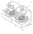
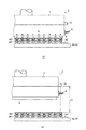
- A Schematic diagram showing the configuration of a temporary crimping head of a semiconductor mounting apparatus according to an embodiment of the present invention
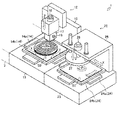
- b Schematic diagram showing the configuration of a cutting head of a semiconductor mounting apparatus according to an embodiment of the present invention
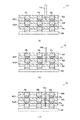
- variety similarly the schematic diagram which shows the aspect cut
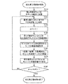
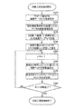
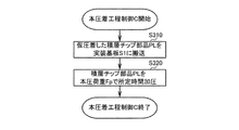
- compression-bonding process of the semiconductor mounting apparatus which concerns on one Embodiment of this invention The figure which shows the flowchart showing the control aspect in the cutting process of the semiconductor mounting apparatus which concerns on one Embodiment of this invention.
- a semiconductor mounting apparatus 1 as an embodiment of the semiconductor mounting apparatus according to the present invention will be described with reference to FIGS.
- the direction in which the semiconductor wafer W is transported from the temporary pressure bonding apparatus 2 to the main pressure bonding apparatus 22 is the X-axis direction, and is perpendicular to the semiconductor wafer W of the temporary pressure bonding head 7, the cutting head 17, and the main pressure bonding head 27 described later.
- a simple moving direction is described as a Z-axis direction, and a direction rotating around the Z-axis is described as a ⁇ direction.
- compression-bonding apparatus 2 are each comprised as embodiment of the semiconductor mounting apparatus 1, it is not limited to this.
- a plurality of chip parts P which are semiconductor elements, are formed on the semiconductor wafer W.
- Each chip component P is formed with a through electrode Pb, and solder Pa is provided at one or both ends of the through electrode Pb.
- a nonconductive film (hereinafter simply referred to as “NCF”) made of a thermosetting resin as an adhesive is attached so as to cover the solder Pa.
- the temporary press-bonded stacked body WL formed by stacking the semiconductor wafers W includes the first semiconductor wafer W1, the second semiconductor wafer W2, the third semiconductor wafer W3,. Yes.
- the temporary press-bonded stacked body WL is composed of a first semiconductor wafer W1, a second semiconductor wafer W2, and a third semiconductor wafer W3.
- the NCF is attached in advance so as to cover the solder Pa of the semiconductor wafer W, but is not limited thereto.
- the semiconductor wafer W is stacked on the support substrate S0.
- the semiconductor mounting apparatus 1 manufactures a semiconductor device in which a plurality of chip parts P are stacked and electrically connected.
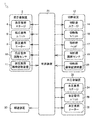
- the semiconductor mounting apparatus 1 includes a provisional pressure bonding device 2, a cutting device 12, a main pressure bonding device 22, a transport device 30, and a control device 31.
- the temporary crimping apparatus 2, the cutting apparatus 12, and the final crimping apparatus 22 are disposed adjacent to each other.
- the temporary crimping device 2 is for temporarily crimping the semiconductor wafers W with an NCF as an adhesive.
- the temporary pressure bonding apparatus 2 is for producing the temporary pressure-bonded laminate WL in which the semiconductor wafers W are stacked.
- the temporary pressure bonding apparatus 2 includes a temporary pressure bonding base 3, a temporary pressure bonding stage 4, a temporary pressure bonding support frame 5, a temporary pressure bonding unit 6, a temporary pressure bonding head 7, a temporary pressure bonding heater 8, and a temporary pressure bonding attachment 9.
- An image recognition device 11 for temporary press bonding is provided.
- the temporary press-bonding base 3 is a main structure constituting the temporary press-bonding device 2.
- the temporary press-bonding base 3 is configured by combining pipe materials and the like so as to have sufficient rigidity.
- the temporary pressure bonding base 3 supports a temporary pressure bonding stage 4 and a temporary pressure bonding support frame 5.
- the temporary press-bonding stage 4 moves the semiconductor wafer W to an arbitrary position while holding the semiconductor wafer W.
- the temporary press-bonding stage 4 is configured by attaching a suction table 4b that can hold the semiconductor wafer W or the support substrate S0 to the drive unit 4a.
- the temporary press-bonding stage 4 is attached to the temporary press-bonding base 3 and is configured so that the suction table 4b can be moved in the X-axis direction, the Y-axis direction, and the ⁇ -direction by the drive unit 4a.
- the pre-bonding stage 4 is configured to be able to move the semiconductor wafer W or the support substrate S0 sucked by the suction table 4b on the temporary press-bonding base 3 in the X-axis direction, the Y-axis direction, and the ⁇ -direction. Yes.
- the temporary press-bonding stage 4 holds the semiconductor wafer W or the support substrate S0 by suction, but is not limited thereto.
- the temporary pressure-bonding support frame 5 supports the temporary pressure-bonding unit 6.
- the temporary press-bonding support frame 5 is formed in a plate shape and is configured to extend from the vicinity of the temporary press-bonding stage 4 of the temporary press-bonding base 3 toward the Z-axis direction.
- the temporary pressure bonding unit 6 which is a pressure unit moves the temporary pressure bonding head 7.
- the temporary crimping unit 6 includes a servo motor and a ball screw (not shown).
- the temporary crimping unit 6 is configured to generate a driving force in the axial direction of the ball screw by rotating the ball screw by a servo motor.
- the temporary crimping unit 6 is attached to the temporary crimping support frame 5 so that the axial direction of the ball screw is in the Z-axis direction perpendicular to the semiconductor wafer W. That is, the temporary crimping unit 6 is configured to generate a driving force (pressing force) in the Z-axis direction.
- the temporary crimping unit 6 is configured such that a temporary crimping load Ft, which is a pressure applied in the Z-axis direction, can be arbitrarily set by controlling the output of the servo motor.
- the provisional pressure bonding unit 6 is composed of a servo motor and a ball screw, but is not limited to this, and may be composed of a pneumatic actuator or a hydraulic actuator.
- the temporary crimping head 7 transmits the driving force of the temporary crimping unit 6 to the semiconductor wafer W.
- the temporary crimping head 7 is attached to a ball screw nut (not shown) constituting the temporary crimping unit 6.
- the temporary crimping unit 6 is disposed so as to face the temporary crimping stage 4. That is, the temporary press-bonding head 7 is configured to be close to the temporary press-bonding stage 4 by being moved in the Z-axis direction by the temporary press-bonding unit 6.
- the temporary pressure bonding head 7 is provided with a temporary pressure bonding heater 8, a temporary pressure bonding attachment 9, and a temporary pressure bonding distance sensor 10 (see FIG. 3A).
- the provisional pressure bonding heater 8 is for heating the semiconductor wafer W.
- the temporary pressure bonding heater 8 is constituted by a cartridge heater and is incorporated in a hole or the like formed in the temporary pressure bonding head 7.
- the provisional pressure bonding heater 8 is composed of a cartridge heater, but is not limited to this, and may be any one that can heat the semiconductor wafer W.
- the temporary crimping attachment 9 holds the semiconductor wafer W and transmits pressure and heat.
- the temporary crimping attachment 9 is provided on the temporary crimping head 7 so as to face the temporary crimping stage 4.
- the temporary crimping attachment 9 is configured to be able to suck and hold the semiconductor wafer W while positioning it.
- the suction holding surface 9 a of the temporary crimping attachment 9 is formed substantially parallel to the temporary crimping stage 4.
- the suction holding surface 9a of the temporary crimping attachment 9 is configured such that the distance to the opposing temporary crimping stage 4 is substantially the same over the entire surface.
- the temporary crimping attachment 9 is configured to be heated by the temporary crimping heater 8. In other words, the temporary crimping attachment 9 is configured to position and hold the semiconductor wafer W and to heat the NCF attached to the semiconductor wafer W by heat transfer from the temporary crimping heater 8.
- the temporary crimping distance sensor 10 measures the distance in the Z-axis direction of the temporary crimping head 7 from an arbitrary reference position.
- the temporary pressure bonding distance sensor 10 is composed of a distance sensor using various laser beams.
- the temporary pressure bonding distance sensor 10 measures a distance from an arbitrary reference position of the temporary pressure bonding head 7 to each semiconductor wafer W temporarily bonded. That is, the temporary press-bonding distance sensor 10 measures the distance L (m) to the m-th semiconductor wafer W (m) after the temporary press-bonding that constitutes the temporary press-bonded laminate WL.
- the temporary pressure bonding distance sensor 10 includes a distance L1 to the first semiconductor wafer W1, a distance L2 to the second semiconductor wafer W2 after the temporary pressure bonding, and a distance L3 to the third semiconductor wafer W3 after the temporary pressure bonding. Measure.
- the provisional pressure-bonding distance sensor 10 is configured by using a laser beam, but is not limited to this, and using an ultrasonic wave, a linear scale, or a servo motor encoder It may consist of what is calculated from
- the temporary pressure bonding image recognition apparatus 11 acquires position information of the semiconductor wafer W from an image.
- the temporary pressure bonding image recognition device 11 recognizes an image of the alignment mark of the semiconductor wafer W held on the temporary pressure bonding stage 4 and the alignment mark of the semiconductor wafer W held on the temporary pressure bonding attachment 9. Thus, the position information of each semiconductor wafer W is obtained.
- the cutting device 12 cuts the temporary press-bonded stacked body WL on which the semiconductor wafers W are stacked. That is, the cutting device 12 is for producing the temporarily-bonded laminated chip component PL.
- the cutting device 12 includes a cutting base 13, a cutting stage 14, a cutting support frame 15, a cutting unit 16, a cutting head 17, a dicing blade 18 as a cutting means, and a cutting distance sensor 19 as a distance measuring means. And an image recognition device 20 for cutting. Note that the cutting base 13, the cutting stage 14, the cutting support frame 15, and the cutting image recognition device 20 have substantially the same configuration as that of the temporary press-bonding device 2. Omitted and the description will focus on the differences.
- the cutting unit 16 moves the cutting head 17.
- the cutting unit 16 includes a moving servo motor (not shown) and a ball screw.
- the cutting unit 16 is configured to generate a driving force in the axial direction of the ball screw by rotating the ball screw with a servo motor.
- the cutting unit 16 is attached to the cutting support frame 15 so that the moving direction is the Z-axis direction perpendicular to the semiconductor wafer W. That is, the cutting unit 16 is configured to generate a driving force (pressing force) in the Z-axis direction while moving the cutting head 17 to an arbitrary position.
- the cutting unit 16 is configured so that a cutting load Fc, which is a pressing force in the Z-axis direction, can be arbitrarily set by controlling the output of the servo motor.
- the cutting unit 16 is composed of a servo motor and a ball screw, but is not limited thereto, and may be composed of a pneumatic actuator or a hydraulic actuator.
- the cutting head 17 transmits the driving force of the cutting unit 16 to the semiconductor wafer W and selectively rotates a plurality of dicing blades 18 serving as cutting means.
- the cutting head 17 is attached to a ball screw nut (not shown) constituting the cutting unit 16.
- the temporary crimping unit 6 is disposed so as to face the cutting stage 14. That is, the cutting head 17 is configured to be close to the cutting stage 14 by being moved in the Z-axis direction by the cutting unit 16.
- the cutting head 17 is provided with a motor for a dicing blade 18 (not shown), a plurality of dicing blades 18 and a cutting distance sensor 19 (see FIG. 3B).
- the dicing blade 18 serving as a cutting means is a blade for cutting the semiconductor wafer W.
- the dicing blade 18 is rotatably provided on the cutting head 17.
- a plurality of dicing blades 18 having different blade widths according to the number of stacked semiconductor wafers W are provided.
- the dicing blade 18 has the first dicing blade 18a, the second dicing blade 18b, and the third dicing blade 18c as the cutting head 17 in order of increasing blade width. Is provided.
- the first dicing blade 18a, the second dicing blade 18b, and the third dicing blade 18c are configured to be housed inside the cutting head 17 (see the black arrow in FIG. 3B), and the temporary press-bonded laminate WL to be cut. Used selectively depending on the layer.
- the cutting distance sensor 19 measures the distance in the Z-axis direction from an arbitrary reference position.
- the cutting distance sensor 19 is composed of a displacement sensor using various laser beams.
- the cutting distance sensor 19 is configured to measure a distance L (n) to an nth semiconductor wafer W (n), which is a distance from an arbitrary reference position of the cutting head 17 to the provisional pressure-bonded stacked body WL. Yes.
- the cutting distance sensor 19 is configured by using a laser beam, but is not limited to this. From the ultrasonic sensor, a linear scale, or an encoder of a servo motor. You may comprise from what calculates.
- the present crimping device 22 adheres the chip components P to each other with NCF, which is an adhesive, and melts the solder Pa to electrically connect with the penetrating electrodes Pb of the adjacent chip components P. is there.
- the main crimping device 22 is for producing the multilayer chip component PL that is finally crimped.
- the main pressure bonding device 22 includes a main pressure bonding base 23, a main pressure bonding stage 24, a main pressure bonding support frame 25, a main pressure bonding unit 26, a main pressure bonding head 27, a main pressure bonding heater 28, and a main pressure bonding attachment 29. It has.
- main pressure bonding base 23, the main pressure bonding stage 24, the main pressure bonding support frame 25, and the main pressure bonding heater 28 have substantially the same configuration as that of the temporary pressure bonding apparatus 2, and therefore the same points are specifically described. The description will be omitted, and the description will focus on the differences.
- the main pressure bonding unit 26 which is a pressure unit, moves the main pressure bonding head 27.
- the main crimping unit 26 includes a servo motor and a ball screw (not shown).
- the main crimping unit 26 is configured to generate a driving force in the axial direction of the ball screw by rotating the ball screw with a servo motor.
- the main crimping unit 26 is attached to the support frame so that the axial direction of the ball screw is in the Z-axis direction perpendicular to the semiconductor wafer W. That is, the main crimping unit 26 is configured to generate a driving force (pressing force) in the Z-axis direction.
- the main press-bonding unit 26 is configured so that a main press-fit load Fp, which is a pressing force in the Z-axis direction, can be arbitrarily set by controlling the output of the servo motor.
- the main crimping unit 26 includes a servo motor and a ball screw.
- the present invention is not limited to this, and may be composed of a pneumatic actuator or a hydraulic actuator.
- the main press-bonding head 27 transmits the driving force of the main press-bonding unit 26 to the laminated chip component PL that has been temporarily press-bonded uniformly.
- the main crimping head 27 is attached to a ball screw nut (not shown) constituting the main crimping unit 26. Further, the main press bonding unit 26 is disposed so as to face the main press bonding stage 24. That is, the main crimping unit 26 is configured to be close to the final crimping stage 24 by being moved in the Z-axis direction by the main crimping unit 26.
- the main pressure bonding head 27 is provided with a main pressure bonding heater 28 and a main pressure bonding attachment 29.
- the main attachment 29 is for contacting the laminated chip part PL that has been preliminarily pressed to transmit pressure and heat.
- the main crimping attachment 29 is provided on the main crimping head 27 so as to face the main crimping stage 24.
- the main press-bonding attachment 29 is formed with a main press-contact contact surface 29a capable of collectively pressing a plurality of temporarily press-bonded laminated chip parts PL.
- the main crimping contact surface 29 a is formed substantially parallel to the final crimping stage 24. Thereby, the main pressing contact surface 29a is configured so that the distance to the opposing main pressing stage 24 is substantially the same over the entire surface.
- the main press-bonding attachment 29 is configured such that the main press-contact contact surface 29a comes into contact with the plurality of provisionally press-bonded laminated chip parts PL almost simultaneously and can be collectively pressed. Further, the main crimping attachment 29 is configured to be heated by the main crimping heater 28. That is, the main crimping attachment 29 transfers the heat of the main crimping heater 28 to the plurality of provisionally crimped laminated chip parts PL under the same conditions, and the plurality of provisionally crimped laminated chip parts PL are collectively and substantially simultaneously. It is comprised so that pressurization is possible.
- the transport device 30 delivers the temporary press-bonded laminate WL between the temporary press-bonding device 2 and the cutting device 12, and is temporarily press-bonded between the cutting device 12 and the main press-bonding device 22.
- the multilayer chip component PL is delivered.
- the transport device 30 transports the support substrate S0 on which the temporary press-bonded laminate WL is disposed from the temporary press-bonding stage 4 of the temporary press-bonding device 2 to the temporary press-bonding stage 4 of the temporary press-bonding device 2, A plurality of provisionally pressure-bonded laminated chip parts PL are transferred from the stage 4 to the mounting substrate S1 on the main pressure bonding stage 24 of the main pressure bonding apparatus 22.
- the control device 31 controls the temporary pressure bonding device 2, the cutting device 12, the main pressure bonding device 22, the transport device 30, and the like.
- the control device 31 may actually have a configuration in which a CPU, a ROM, a RAM, an HDD, and the like are connected by a bus, or may be configured by a one-chip LSI or the like.
- the control device 31 stores various programs and data for controlling the provisional pressure bonding device 2, the cutting device 12, the main pressure bonding device 22, the conveying device 30, and the like.
- the control device 31 is connected to the pre-crimping stage 4, the cutting stage 14, and the main crimping stage 24, and the X-axis direction and Y-axis of the temporary crimping stage 4, the cutting stage 14, and the main crimping stage 24 are The amount of movement in the direction and ⁇ direction can be controlled.
- the control device 31 is connected to the temporary pressure bonding heater 8 and the main pressure bonding heater 28, and can control the temperatures of the temporary pressure bonding heater 8 and the main pressure bonding heater 28, respectively.
- the control device 31 is connected to the provisional pressure bonding unit 6, the cutting unit 16, and the main pressure bonding unit 26, and the pressing force in the X-axis direction of the temporary pressure bonding unit 6, the cutting unit 16, and the main pressure bonding unit 26. And the operation mode of the dicing blade 18 of the cutting unit 16 can be controlled.
- the control device 31 is connected to the temporary crimping attachment 9 and can control the suction state of the temporary crimping attachment 9.
- the control device 31 is connected to the temporary pressure bonding image recognition device 11 and the cutting image recognition device 20, and controls the temporary pressure bonding image recognition device 11 and the cutting image recognition device 20, respectively.
- the position information of the stacked body WL can be acquired.
- the control device 31 is connected to the transport device 30 and can control the transport device 30.
- the control device 31 is connected to the temporary pressure bonding distance sensor 10 and the cutting distance sensor 19, and is a distance L (m) to each layer in the temporary pressure bonding laminate WL measured by the temporary pressure bonding distance sensor 10 (distance in the present embodiment). L1, L2, L3) and a distance L (n) (distance L3 in the present embodiment) that is a distance between the temporary pressure-bonded laminate WL measured by the cutting distance sensor 19 can be acquired.
- the first semiconductor will be described with reference to FIGS. 5 to 7 regarding the control of the gap between the solder Pa and the through electrode Pb of the adjacent semiconductor wafer W using the NCF when the semiconductor mounting apparatus 1 according to the present invention is temporarily crimped. Description will be made using the wafer W1 and the second semiconductor wafer W2.
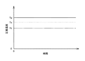
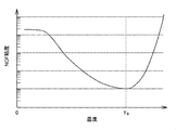
- the viscosity of NCF varies depending on its temperature. Specifically, an NCF composed of a thermosetting resin does not cure in a temperature range below the reference temperature Ts (see FIG. 5) determined from the characteristics of the NCF, and has a viscosity reversibly as the temperature rises. It shows the property of being lowered. On the other hand, NCF is hardened in a temperature range equal to or higher than the reference temperature Ts, and irreversibly shows a property that its viscosity increases with increasing temperature.
- the semiconductor mounting apparatus 1 uses a temporary crimping heater 8 to hold the second semiconductor wafer W2 sucked and held by the temporary crimping attachment 9 of the temporary crimping apparatus 2 in the temporary crimping process.
- Heat to pre-bonding temperature Tt Along with this, the NCF (see FIG. 7) attached so as to cover the solder Pa of the second semiconductor wafer W2 transmits the heat of the second semiconductor wafer W2 and is approximately the same provisional pressure bonding as the second semiconductor wafer W2. Heated to temperature Tt.
- the temporary pressure bonding temperature Tt is set lower than the reference temperature Ts. That is, the semiconductor mounting apparatus 1 controls the temperature of the provisional pressure bonding heater 8 so that the NCF has a predetermined viscosity in a temperature range where the NCF is not cured.
- the semiconductor mounting apparatus 1 moves the second semiconductor wafer W2 heated to the temporary pressure bonding temperature Tt toward the first semiconductor wafer W1 by the temporary pressure bonding unit 6 in the Z-axis direction.
- the NCF attached so as to cover the solder Pa contacts the pads Ca on the semiconductor wafer W.
- a temporary press-bonding load Ft is applied in the Z-axis direction from the temporary press-bonding unit 6 because the NCF contacts the through electrode Pb of the first semiconductor wafer W1.
- the NCF of the second semiconductor wafer W2 is deformed by the temporary pressure bonding load Ft of the temporary pressure bonding unit 6. At this time, a reaction force is generated on the second semiconductor wafer W2 due to the viscous resistance of the NCF with respect to the temporary pressure bonding load Ft.
- the reaction force due to the viscous resistance of the NCF generated in the second semiconductor wafer W2 increases according to the deformation amount of the NCF sandwiched between the through electrode Pb of the first semiconductor wafer W1 and the solder Pa of the second semiconductor wafer W2.
- the position of the second semiconductor wafer W2 in the Z-axis direction in the temporary press-bonding step is determined by the temporary press-fit load Ft and the NCF viscosity. Accordingly, as shown in FIG. 7C, the semiconductor mounting apparatus 1 uses the temporary pressure bonding apparatus 2 to set the temporary pressure bonding load Ft by the temporary pressure bonding unit 6 and the temperature of the temporary pressure bonding heater 8 for setting the NCF viscosity.
- the gap between the through electrode Pb of the first semiconductor wafer W1 and the solder Pa of the second semiconductor wafer W2 can be set within an arbitrary predetermined range Gt.
- the position of the second semiconductor wafer W2 in the Z-axis direction can also be controlled by the temporary pressure bonding load Ft and the temporary pressure bonding time at an arbitrary viscosity of NCF.
- the manufacturing method of the multilayer chip component PL includes a temporary pressure bonding step, a cutting step, and a main pressure bonding step.
- the multilayer chip component PL is a memory device.
- the semiconductor mounting apparatus 1 uses the pre-bonding stage of the pre-bonding device 2 to hold the first semiconductor wafer W ⁇ b> 1 held by the temporary bonding attachment 9 of the pre-bonding apparatus 2. 4 is arranged on the support substrate S0 held by suction. Further, the semiconductor mounting apparatus 1 is heated to the temporary pressure bonding temperature Tt by the temporary pressure bonding heater 8 of the temporary pressure bonding apparatus 2 while holding the second semiconductor wafer W2 by the temporary pressure bonding attachment 9. The temporary pressure bonding temperature Tt is set lower than the reference temperature Ts (see FIG. 5). That is, the semiconductor mounting apparatus 1 controls the temperature of the provisional pressure bonding heater 8 so that the NCF has a predetermined viscosity in a temperature range where the NCF is not cured.
- the semiconductor mounting apparatus 1 is configured so that the solder Pa or the through electrode Pb of the first semiconductor wafer W1 and the solder Pa or the through electrode Pb of the second semiconductor wafer W2 overlap each other in the X axis direction and the Y axis direction of the second semiconductor wafer W2. , ⁇ alignment is performed. Then, the semiconductor mounting apparatus 1 temporarily press-bonds the second semiconductor wafer W2 to the first semiconductor wafer W1 while pressurizing the second semiconductor wafer W2 with the temporary press-bonding load Ft by the temporary bonding attachment 9. At this time, the semiconductor mounting apparatus 1 temporarily press-fits the gap between the through electrode Pb of the first semiconductor wafer W1 and the solder Pa of the second semiconductor wafer W2 within a predetermined range Gt (see FIG.
- the predetermined range Gt is preferably 1 to 5 ⁇ m, more preferably 1 to 3 ⁇ m. This value is an experimentally obtained value.
- a connection process described later is performed. It has been found that the adhesive 7 may remain between the through electrode Pb and the solder Pa when both are connected. This is considered to be because the solder melts and entrains NCF by heating to the melting point of the solder. Further, if the gap is made wider than this value, a positional shift may occur in the main press bonding step, which becomes a serious problem in quality.
- the semiconductor mounting apparatus 1 measures a distance L2 from an arbitrary reference position of the temporary crimping head 7 to the second semiconductor wafer W2. Similarly, the semiconductor mounting apparatus 1 allows the m-th semiconductor wafer W (m) to be attached by the temporary crimping attachment 9 until the temporary crimped laminate WL is formed (in this embodiment, three layers of the temporary crimped laminate WL). A pressure is temporarily applied to the (m ⁇ 1) th semiconductor wafer W (m ⁇ 1) while being heated to the temporary pressure bonding temperature Tt while being pressurized with a temporary pressure bonding load Ft, and a distance L (m) is measured.
- the semiconductor mounting apparatus 1 produces the temporary press-bonded laminate WL in the temporary press-bonding step.
- the semiconductor mounting apparatus 1 may be configured to be heated to a temporary press-bonding temperature Tt in a vacuum furnace and pressurized with a temporary press-bonding load Ft.
- the semiconductor mounting apparatus 1 sucks and holds the n-layer temporary press-bonded stacked body WL transported to the cutting stage 14 of the cutting apparatus 12 by the transport apparatus 30.
- the semiconductor mounting apparatus 1 is provided for each semiconductor wafer W constituting the temporary press-bonded laminate WL based on the measured value of the temporary press-bonding distance sensor 10 of the temporary press-bonding apparatus 2 and the measured value of the cutting distance sensor 19 of the cutting apparatus 12. Cutting is performed by the dicing blade 18 of the cutting device 12.
- FIG. 9 As shown in FIG.
- the semiconductor mounting apparatus 1 uses the third dicing blade 18 c of the cutting apparatus 12 to remove only the uppermost third semiconductor wafer W ⁇ b> 3 of the three-layer temporary press-bonded stacked body WL. Disconnect. At this time, the semiconductor mounting apparatus 1 cuts the third semiconductor wafer W3 along the shape of the temporarily press-bonded laminated chip part PL. Further, as shown in FIG. 9B, the semiconductor mounting apparatus 1 removes only the second semiconductor wafer W ⁇ b> 2 from the third dicing blade based on the distance L ⁇ b> 2 that is a measurement value of the temporary pressure bonding distance sensor 10 of the temporary pressure bonding apparatus 2. It cut
- the semiconductor mounting apparatus 1 cuts only the first semiconductor wafer W ⁇ b> 1 with the first dicing blade 18 a having a blade width smaller than that of the second dicing blade 18. In this way, in the cutting process, the semiconductor mounting apparatus 1 uses the dicing plate 18 that is thinner than the cutting width in order to prevent the laminated chip component PL that has been temporarily press-bonded while suppressing contact between the dicing plate and the semiconductor wafer W. Make it. As shown in FIG. 10A, after cutting the temporary press-bonded stacked body WL, the semiconductor mounting apparatus 1 includes defective chip components based on information on defective chip components of each semiconductor wafer W acquired from the upstream process.
- the laminated chip parts PL other than the laminated chip part PLd are conveyed by the conveying device 30 to the final crimping stage 24 of the final crimping device 22. That is, the semiconductor mounting apparatus 1 excludes the multilayer chip component PLd including the defective chip component based on the information about the defective chip component. Since the NCF is cut at the same time as the semiconductor wafer W, there is almost no protrusion of NCF in the laminated chip component PL after dicing (extrusion of 1 ⁇ m or less). The state in which the NCF does not protrude from the multilayer chip component PL can be confirmed by observing the cut surface with an optical microscope.
- the semiconductor mounting apparatus 1 is subjected to a plurality of temporary crimping operations on the mounting substrate S ⁇ b> 1 held by the final crimping stage 24 of the final crimping apparatus 22.
- the laminated chip component PL is conveyed to a predetermined position.
- the semiconductor mounting apparatus 1 heats the main press-bonding attachment 29 of the main press-bonding apparatus 22 to the main press-bonding temperature Tp by bringing the plurality of temporarily-bonded laminated chip parts PL into contact with each other.
- the main pressure bonding temperature Tp is set within a certain range that is equal to or higher than the reference temperature Ts and equal to or higher than the melting point of the solder Pa (see FIG.
- the semiconductor mounting apparatus 1 controls the temperature of the main pressure bonding heater 28 so that the NCF has a predetermined main pressure viscosity (hardness) and the solder Pa is melted in a temperature range where the NCF is cured. . Furthermore, the semiconductor mounting apparatus 1 collectively presses a plurality of provisionally press-bonded laminated chip parts PL with the main press-bonding attachment 29 with a main press-fit load Fp. Each chip component P is close to each other so as to eliminate the gap between the through electrode Pb and the solder Pa.
- the temporarily chip-bonded multilayer chip component PL is fixed (main press-bonding) between adjacent chip components P by thermosetting NCF, and the solder Pa is melted to be electrically connected to the through electrode Pb of the adjacent chip component P. Is done.
- the plurality of chip parts P are in contact with the contact surface 29a for main press-bonding 29 of the main press-bond attachment 29 substantially simultaneously and uniformly. That is, the plurality of chip components P are finally press-bonded by the main press-bonding device 22 in a state in which the heating time, the heating time, the applied pressure, and the like are substantially the same.
- control mode for manufacturing a semiconductor device including the n-layer laminated chip component PL in the semiconductor manufacturing apparatus 1 according to the present invention.
- the temporary crimping heater 8 is maintained in advance at a temperature necessary for heating the chip component P to the temporary crimping temperature Tt, and the final crimping heater 28 is configured to maintain the chip component P at the final crimping temperature. It is assumed that the temperature necessary for heating to Tp is maintained in advance.
- the control device 31 acquires position information of a defective chip component among the chip components P formed on the first semiconductor wafer W1, the second semiconductor wafer W2, and the third semiconductor wafer W3 from the upstream process. To do.
- step S100 the control device 31 starts the temporary crimping process control A and shifts the step to step 110 (see FIG. 12). Then, when the temporary pressure bonding process control A is completed, the step is shifted to step S200.
- step S200 the control device 31 starts the cutting process control B and shifts the step to step 210 (see FIG. 13). And when cutting process control B is complete
- step S300 the control device 31 starts the main crimping process control C and shifts the step to step S310 (see FIG. 14). Then, when the main crimping process control C is finished, the step is finished.
- step S120 the control device 31 measures the distance L (m) in the Z-axis direction from an arbitrary reference position of the temporary crimping unit 6 to the m-th semiconductor wafer W (m) by the temporary crimping distance sensor 10. The step moves to step S130.
- step S140 the control device 31 sucks and holds the m-th semiconductor wafer W (m) by the temporary pressure bonding attachment 9 of the temporary pressure bonding head 7, and shifts the step to step S150 (m ⁇ 2).
- step S150 the control device 31 aligns the alignment mark of the m-th semiconductor wafer W (m) held by the temporary pressure-bonding attachment 9 of the temporary pressure-bonding head 7 and the temporary pressure-bonding image recognition device 11 with the temporary pressure-bonding image recognition device 11. Image information with the alignment mark of the (m ⁇ 1) th semiconductor wafer W (m ⁇ 1) held by suction on the stage 4 is acquired, and the process proceeds to step S160.
- step S160 the control device 31 determines the m ⁇ 1th semiconductor wafer W (m ⁇ ) based on the acquired image information of the m ⁇ 1th semiconductor wafer W (m ⁇ 1) and the mth semiconductor wafer W (m). 1) Calculate the coordinate positions of the temporary press-bonding stage 4 in the X-axis direction, Y-axis direction, and ⁇ -direction for alignment between the m-th semiconductor wafer W (m) and the suction table 4b of the temporary press-fit stage 4 Is moved by the drive unit 4a, and the process proceeds to step S170.
- step S170 the control device 31 temporarily press-bonds the m-th semiconductor wafer W (m) held by suction attachment 9 to the m-1th semiconductor wafer W (m-1) of the pre-bonding stage 4.
- the unit 6 applies pressure for a predetermined time with a temporary pressure bonding load Ft to perform temporary pressure bonding, and the step proceeds to step S180.
- the control device 31 completes the temporary crimping process control A and shifts the step to step S200 (see FIG. 11).
- the control device 31 shifts the step to step S120.
- step S ⁇ b> 210 the control device 31 sucks the support substrate S ⁇ b> 0 (temporary pressure-bonded laminate WL) transported from the temporary press-bonding stage 4 by the transport device 30 by the suction table 14 b of the cutting stage 14. The step is shifted to step S220.
- step S220 the control device 31 acquires the image information of the alignment mark of the temporary press-bonded laminate WL that is sucked and held by the cutting stage 14 by the cutting image recognition device 20, and shifts the step to step S230.
- step S230 the control device 31 determines the coordinate positions in the X-axis direction, Y-axis direction, and ⁇ -direction of the cutting stage 14 for alignment of the temporary press-bonded laminate WL based on the image information of the temporary press-bonded laminate WL. And the suction table 14b of the cutting stage 14 is moved by the drive unit 14a, and the process proceeds to step S240.
- step S240 the control device 31 measures the distance L (n) in the Z-axis direction from an arbitrary reference position of the cutting unit 16 to the nth semiconductor wafer W (n), and corrects the error in the height direction.
- the step is shifted to step S250.
- step S260 the control device 31 moves the cutting head 17 to cut only the m-th semiconductor wafer W (m) based on the distance L (m) in the Z-axis direction measured in the temporary pressure bonding process control A. The amount is calculated, and the process proceeds to step S270.
- step S270 the control device 31 rotates and drives the predetermined dicing blade 18 to cut only the mth semiconductor wafer W (m) in the temporary press-bonded stacked body WL along the shape of the chip component P.
- the process proceeds to S280.
- step S280 the control device 31 determines whether or not the cutting of the first semiconductor wafer W1 has been completed by the provisional pressure bonding unit 6.
- control device 31 performs the cutting process. Control B is terminated and the process proceeds to step S300 (see FIG. 9).
- control device 31 Shifts the step to step S250.
- step S ⁇ b> 310 the control device 31 puts the multilayer chip component PL other than the temporarily-crimped multilayer chip component PLd including the defective chip component by the transport device 30 on the suction table 24 b of the main crimping stage 24. It arrange
- step S320 the control device 31 presses and fixes the plurality of provisionally press-bonded laminated chip parts PL with the main press-bonding unit 26 with a main press-fit load Fp for a predetermined time, and ends the main press-bonding process control C. finish.
- a memory device having a stacked structure is manufactured.
- the semiconductor mounting apparatus 1 stacks the first semiconductor wafer W1, the second semiconductor wafer W2, and the third semiconductor wafer W3 on which the plurality of chip components P are formed on the support substrate S0. That is, by using the support substrate S0 in the temporary press-bonding process, the semiconductor mounting apparatus 1 simultaneously manufactures a plurality of multilayer chip components PL that are memory devices while suppressing warpage of the semiconductor wafer W and the like. Furthermore, the semiconductor mounting apparatus 1 cuts the temporary press-bonded stacked body WL by selectively using a plurality of dicing plates 18 having different blade widths.
- the semiconductor mounting apparatus 1 is temporarily pressure-bonded while cutting the next semiconductor wafer W with the dicing blade 18 thinner than the cutting width, thereby suppressing a shift at the time of cutting due to contact with the dicing plate 18 or the like.
- the laminated chip component PL is produced.
- the semiconductor mounting apparatus 1 performs main pressure bonding after cutting the temporary pressure-bonded stacked body WL within a predetermined range Gt in which the gap between the adjacent through electrode Pb and the solder Pa is sufficiently small. That is, the semiconductor mounting apparatus 1 manufactures the multilayer chip component PL that is a memory device while suppressing the generation of voids and the shift at the time of cutting in the cutting process and the main pressure bonding process.
- the semiconductor mounting apparatus 1 eliminates the multilayer chip component PLd including the defective chip component based on the information about the defective chip component. That is, the semiconductor mounting apparatus 1 eliminates defective multilayer chip components PLd due to reasons other than cutting. As a result, the manufacturing time of a semiconductor device such as a memory device in which the chip components P are stacked can be shortened, and the occurrence of defective bonding between the chip components P can be suppressed. Moreover, the semiconductor mounting apparatus 1 suppresses generation
Landscapes
- Wire Bonding (AREA)
- Engineering & Computer Science (AREA)
- Manufacturing & Machinery (AREA)
- Container, Conveyance, Adherence, Positioning, Of Wafer (AREA)
- Die Bonding (AREA)
Abstract
Description
18 ダイシングブレード
P チップ部品
Pa はんだ
Pb 貫通電極
NCF 接着剤
W(n) 半導体ウェハ
Ft 仮圧着荷重
Fp 本圧着荷重
Claims (7)
- チップ部品が形成された複数の半導体ウェハを積層して電気的に接続する半導体装置の製造方法であって、
接着剤を介して複数の半導体ウェハを積層し、接着剤が所定の粘度になるように加熱するとともに、チップ部品毎に設けられた貫通電極のはんだと隣接する半導体ウェハの貫通電極との間隙がゼロよりも大きい所定の範囲内に収まるように半導体ウェハを仮圧着荷重で加圧して仮圧着積層体を作製する仮圧着工程と、
仮圧着積層体を切断手段で切断してチップ部品が積層された仮圧着された積層チップ部品を作製する切断工程と、
仮圧着された積層チップ部品を接着剤の硬化温度以上かつはんだの融点以上に加熱するとともに、はんだが隣接するチップ部品の貫通電極に接触するように仮圧着された積層チップ部品を本圧着荷重で加圧して本圧着された積層チップ部品を作製する本圧着工程と、
を含む半導体装置の製造方法。 - 前記切断工程において、前記切断手段が積層された前記半導体ウェハを一枚ずつ切断する請求項1に記載の半導体装置の製造方法。
- 前記切断工程において、前記切断手段がダイシングブレードから構成され、前記半導体ウェハを切断する度にダイシングブレードのブレード幅を小さくする請求項1または請求項2に記載の半導体装置の製造方法。
- 前記仮圧着工程において、前記半導体ウェハを真空中で加熱および加圧する請求項1から請求項3のいずれか一項に記載の半導体装置の製造方法。
- 前記仮圧着工程において、サポート基板上に前記半導体ウェハを積層し、加熱および加圧した後に作製した仮圧着積層体からサポート基板を取り除く請求項1から請求項3のいずれか一項に記載の半導体装置の製造方法。
- 請求項1から請求項5のいずれか一項に記載の半導体装置の製造方法で製造されたメモリデバイス。
- チップ部品が形成された複数の半導体ウェハを積層して電気的に接続する半導体装置の製造装置であって、
接着剤を介して複数の半導体ウェハを積層し、接着剤が所定の粘度になるように加熱するとともに、チップ部品毎に設けられた貫通電極のはんだと隣接する半導体ウェハの貫通電極との間隙がゼロよりも大きい所定の範囲内に収まるように半導体ウェハを仮圧着荷重で加圧して仮圧着積層体を作製する仮圧着装置2と、
仮圧着積層体を切断手段で切断してチップ部品が積層された仮圧着された積層チップ部品を作製する切断装置と、
各半導体ウェハに形成されているチップ部品のうち不良チップ部品の位置を予め取得し、作製した仮圧着された積層チップ部品のうち不良チップ部品が含まれる仮圧着された積層チップ部品を排出する排出手段と、
を具備する半導体実装装置。
Priority Applications (3)
| Application Number | Priority Date | Filing Date | Title |
|---|---|---|---|
| JP2017510015A JPWO2016158935A1 (ja) | 2015-03-30 | 2016-03-29 | 半導体装置の製造方法、半導体実装装置および半導体装置の製造方法で製造されたメモリデバイス |
| US15/562,501 US10181460B2 (en) | 2015-03-30 | 2016-03-29 | Method for manufacturing semiconductor device, semiconductor mounting device, and memory device manufactured by method for manufacturing semiconductor device |
| KR1020177028864A KR20170128445A (ko) | 2015-03-30 | 2016-03-29 | 반도체 장치의 제조 방법, 반도체 실장 장치 및 반도체 장치의 제조 방법으로 제조된 메모리 디바이스 |
Applications Claiming Priority (2)
| Application Number | Priority Date | Filing Date | Title |
|---|---|---|---|
| JP2015-069740 | 2015-03-30 | ||
| JP2015069740 | 2015-03-30 |
Publications (1)
| Publication Number | Publication Date |
|---|---|
| WO2016158935A1 true WO2016158935A1 (ja) | 2016-10-06 |
Family
ID=57007211
Family Applications (1)
| Application Number | Title | Priority Date | Filing Date |
|---|---|---|---|
| PCT/JP2016/060079 Ceased WO2016158935A1 (ja) | 2015-03-30 | 2016-03-29 | 半導体装置の製造方法、半導体実装装置および半導体装置の製造方法で製造されたメモリデバイス |
Country Status (5)
| Country | Link |
|---|---|
| US (1) | US10181460B2 (ja) |
| JP (1) | JPWO2016158935A1 (ja) |
| KR (1) | KR20170128445A (ja) |
| TW (1) | TW201705368A (ja) |
| WO (1) | WO2016158935A1 (ja) |
Cited By (1)
| Publication number | Priority date | Publication date | Assignee | Title |
|---|---|---|---|---|
| JP2024006497A (ja) * | 2022-07-01 | 2024-01-17 | 株式会社ディスコ | 加工方法 |
Families Citing this family (6)
| Publication number | Priority date | Publication date | Assignee | Title |
|---|---|---|---|---|
| US10669454B2 (en) * | 2015-10-29 | 2020-06-02 | Hitachi Chemical Company, Ltd. | Method for manufacturing semiconductor device including heating and pressuring a laminate having an adhesive layer |
| JP6477971B2 (ja) | 2016-05-09 | 2019-03-06 | 日立化成株式会社 | 半導体装置の製造方法 |
| JP6349540B2 (ja) * | 2016-10-06 | 2018-07-04 | 株式会社新川 | 半導体チップの実装装置、および、半導体装置の製造方法 |
| DE102018124492A1 (de) * | 2018-10-04 | 2020-04-09 | Osram Opto Semiconductors Gmbh | Vorrichtung und verfahren zur prozessierung einer vielzahl von halbleiterchips |
| TWI775111B (zh) * | 2020-07-15 | 2022-08-21 | 歆熾電氣技術股份有限公司 | 晶片承載結構與晶片安裝方法 |
| KR102900083B1 (ko) | 2021-03-10 | 2025-12-12 | 삼성전자주식회사 | 반도체 패키지 |
Citations (7)
| Publication number | Priority date | Publication date | Assignee | Title |
|---|---|---|---|---|
| JP2007250886A (ja) * | 2006-03-16 | 2007-09-27 | Toshiba Corp | 半導体装置の製造方法 |
| JP2008130706A (ja) * | 2006-11-20 | 2008-06-05 | Sony Corp | 半導体装置の製造方法 |
| JP2008294382A (ja) * | 2007-04-27 | 2008-12-04 | Sumitomo Bakelite Co Ltd | 半導体ウエハーの接合方法および半導体装置の製造方法 |
| WO2010109985A1 (ja) * | 2009-03-25 | 2010-09-30 | 株式会社村田製作所 | 電子部品の製造方法 |
| JP2012160634A (ja) * | 2011-02-02 | 2012-08-23 | Nec Corp | モジュール部品およびその製造方法 |
| JP2013065835A (ja) * | 2011-08-24 | 2013-04-11 | Sumitomo Bakelite Co Ltd | 半導体装置の製造方法、ブロック積層体及び逐次積層体 |
| WO2013133015A1 (ja) * | 2012-03-07 | 2013-09-12 | 東レ株式会社 | 半導体装置の製造方法および半導体装置の製造装置 |
Family Cites Families (2)
| Publication number | Priority date | Publication date | Assignee | Title |
|---|---|---|---|---|
| US8039305B2 (en) | 2007-04-27 | 2011-10-18 | Sumitomo Bakelite Company, Ltd. | Method for bonding semiconductor wafers and method for manufacturing semiconductor device |
| JP5780228B2 (ja) | 2011-11-11 | 2015-09-16 | 住友ベークライト株式会社 | 半導体装置の製造方法 |
-
2016
- 2016-03-29 KR KR1020177028864A patent/KR20170128445A/ko not_active Ceased
- 2016-03-29 WO PCT/JP2016/060079 patent/WO2016158935A1/ja not_active Ceased
- 2016-03-29 TW TW105109940A patent/TW201705368A/zh unknown
- 2016-03-29 JP JP2017510015A patent/JPWO2016158935A1/ja active Pending
- 2016-03-29 US US15/562,501 patent/US10181460B2/en active Active
Patent Citations (7)
| Publication number | Priority date | Publication date | Assignee | Title |
|---|---|---|---|---|
| JP2007250886A (ja) * | 2006-03-16 | 2007-09-27 | Toshiba Corp | 半導体装置の製造方法 |
| JP2008130706A (ja) * | 2006-11-20 | 2008-06-05 | Sony Corp | 半導体装置の製造方法 |
| JP2008294382A (ja) * | 2007-04-27 | 2008-12-04 | Sumitomo Bakelite Co Ltd | 半導体ウエハーの接合方法および半導体装置の製造方法 |
| WO2010109985A1 (ja) * | 2009-03-25 | 2010-09-30 | 株式会社村田製作所 | 電子部品の製造方法 |
| JP2012160634A (ja) * | 2011-02-02 | 2012-08-23 | Nec Corp | モジュール部品およびその製造方法 |
| JP2013065835A (ja) * | 2011-08-24 | 2013-04-11 | Sumitomo Bakelite Co Ltd | 半導体装置の製造方法、ブロック積層体及び逐次積層体 |
| WO2013133015A1 (ja) * | 2012-03-07 | 2013-09-12 | 東レ株式会社 | 半導体装置の製造方法および半導体装置の製造装置 |
Cited By (2)
| Publication number | Priority date | Publication date | Assignee | Title |
|---|---|---|---|---|
| JP2024006497A (ja) * | 2022-07-01 | 2024-01-17 | 株式会社ディスコ | 加工方法 |
| JP7836240B2 (ja) | 2022-07-01 | 2026-03-26 | 株式会社ディスコ | 加工方法 |
Also Published As
| Publication number | Publication date |
|---|---|
| TW201705368A (zh) | 2017-02-01 |
| JPWO2016158935A1 (ja) | 2018-02-01 |
| KR20170128445A (ko) | 2017-11-22 |
| US20180096980A1 (en) | 2018-04-05 |
| US10181460B2 (en) | 2019-01-15 |
Similar Documents
| Publication | Publication Date | Title |
|---|---|---|
| WO2016158935A1 (ja) | 半導体装置の製造方法、半導体実装装置および半導体装置の製造方法で製造されたメモリデバイス | |
| JP6383449B2 (ja) | 電子部品実装方法および電子部品実装システム | |
| JP6349540B2 (ja) | 半導体チップの実装装置、および、半導体装置の製造方法 | |
| JP5602439B2 (ja) | 加熱装置および実装体の製造方法 | |
| TWI670776B (zh) | 半導體裝置的製造方法以及封裝裝置 | |
| JP6518461B2 (ja) | 実装装置および実装方法 | |
| TW201407696A (zh) | 安裝方法 | |
| WO2016031806A1 (ja) | 実装用ヘッドおよびそれを用いた実装装置 | |
| WO2015199045A1 (ja) | 実装装置および実装方法 | |
| TWI659479B (zh) | 半導體裝置的製造方法以及封裝裝置 | |
| CN110914962A (zh) | 封装装置以及半导体装置的制造方法 | |
| JP4720469B2 (ja) | 貼り合わせ半導体装置製造用の露光方法 | |
| JP2020136650A (ja) | チップ転写板ならびに半導体チップ積層方法および半導体装置の製造方法 | |
| KR102221588B1 (ko) | 반도체 칩 본딩 장치 및 반도체 칩 본딩 방법 | |
| JP2017123423A (ja) | 半導体実装装置および半導体実装方法 | |
| JP6643198B2 (ja) | 半導体装置の製造方法および製造装置 | |
| CN110235230A (zh) | 半导体装置的制造装置和制造方法 | |
| JP6863767B2 (ja) | 実装装置および実装方法 | |
| WO2016125763A1 (ja) | 実装装置および実装方法 | |
| CN111742623A (zh) | 带金属片配线基板以及带金属片配线基板的制造方法 | |
| JP2016189427A (ja) | 実装方法および実装装置 | |
| WO2015105149A1 (ja) | 半導体装置の実装方法および実装装置 | |
| JP2021114523A (ja) | 半導体部品の製造方法及び複合ウェハ | |
| JP2019110187A (ja) | 実装装置及び実装方法 | |
| JP2007251000A (ja) | 半導体装置およびその製造方法並びに製造装置 |
Legal Events
| Date | Code | Title | Description |
|---|---|---|---|
| 121 | Ep: the epo has been informed by wipo that ep was designated in this application |
Ref document number: 16772816 Country of ref document: EP Kind code of ref document: A1 |
|
| ENP | Entry into the national phase |
Ref document number: 2017510015 Country of ref document: JP Kind code of ref document: A |
|
| WWE | Wipo information: entry into national phase |
Ref document number: 15562501 Country of ref document: US |
|
| NENP | Non-entry into the national phase |
Ref country code: DE |
|
| ENP | Entry into the national phase |
Ref document number: 20177028864 Country of ref document: KR Kind code of ref document: A |
|
| 122 | Ep: pct application non-entry in european phase |
Ref document number: 16772816 Country of ref document: EP Kind code of ref document: A1 |