WO2016158698A1 - 光電変換素子 - Google Patents
光電変換素子 Download PDFInfo
- Publication number
- WO2016158698A1 WO2016158698A1 PCT/JP2016/059484 JP2016059484W WO2016158698A1 WO 2016158698 A1 WO2016158698 A1 WO 2016158698A1 JP 2016059484 W JP2016059484 W JP 2016059484W WO 2016158698 A1 WO2016158698 A1 WO 2016158698A1
- Authority
- WO
- WIPO (PCT)
- Prior art keywords
- group
- photoelectric conversion
- conversion element
- represented
- formula
- Prior art date
- Legal status (The legal status is an assumption and is not a legal conclusion. Google has not performed a legal analysis and makes no representation as to the accuracy of the status listed.)
- Ceased
Links
Classifications
-
- H—ELECTRICITY
- H10—SEMICONDUCTOR DEVICES; ELECTRIC SOLID-STATE DEVICES NOT OTHERWISE PROVIDED FOR
- H10K—ORGANIC ELECTRIC SOLID-STATE DEVICES
- H10K85/00—Organic materials used in the body or electrodes of devices covered by this subclass
- H10K85/20—Carbon compounds, e.g. carbon nanotubes or fullerenes
- H10K85/211—Fullerenes, e.g. C60
- H10K85/215—Fullerenes, e.g. C60 comprising substituents, e.g. PCBM
-
- H—ELECTRICITY
- H01—ELECTRIC ELEMENTS
- H01G—CAPACITORS; CAPACITORS, RECTIFIERS, DETECTORS, SWITCHING DEVICES, LIGHT-SENSITIVE OR TEMPERATURE-SENSITIVE DEVICES OF THE ELECTROLYTIC TYPE
- H01G9/00—Electrolytic capacitors, rectifiers, detectors, switching devices, light-sensitive or temperature-sensitive devices; Processes of their manufacture
- H01G9/20—Light-sensitive devices
- H01G9/2004—Light-sensitive devices characterised by the electrolyte, e.g. comprising an organic electrolyte
- H01G9/2009—Solid electrolytes
-
- H—ELECTRICITY
- H10—SEMICONDUCTOR DEVICES; ELECTRIC SOLID-STATE DEVICES NOT OTHERWISE PROVIDED FOR
- H10K—ORGANIC ELECTRIC SOLID-STATE DEVICES
- H10K85/00—Organic materials used in the body or electrodes of devices covered by this subclass
- H10K85/50—Organic perovskites; Hybrid organic-inorganic perovskites [HOIP], e.g. CH3NH3PbI3
-
- H—ELECTRICITY
- H01—ELECTRIC ELEMENTS
- H01G—CAPACITORS; CAPACITORS, RECTIFIERS, DETECTORS, SWITCHING DEVICES, LIGHT-SENSITIVE OR TEMPERATURE-SENSITIVE DEVICES OF THE ELECTROLYTIC TYPE
- H01G9/00—Electrolytic capacitors, rectifiers, detectors, switching devices, light-sensitive or temperature-sensitive devices; Processes of their manufacture
- H01G9/20—Light-sensitive devices
- H01G9/2059—Light-sensitive devices comprising an organic dye as the active light absorbing material, e.g. adsorbed on an electrode or dissolved in solution
-
- H—ELECTRICITY
- H10—SEMICONDUCTOR DEVICES; ELECTRIC SOLID-STATE DEVICES NOT OTHERWISE PROVIDED FOR
- H10K—ORGANIC ELECTRIC SOLID-STATE DEVICES
- H10K30/00—Organic devices sensitive to infrared radiation, light, electromagnetic radiation of shorter wavelength or corpuscular radiation
- H10K30/20—Organic devices sensitive to infrared radiation, light, electromagnetic radiation of shorter wavelength or corpuscular radiation comprising organic-organic junctions, e.g. donor-acceptor junctions
-
- H—ELECTRICITY
- H10—SEMICONDUCTOR DEVICES; ELECTRIC SOLID-STATE DEVICES NOT OTHERWISE PROVIDED FOR
- H10K—ORGANIC ELECTRIC SOLID-STATE DEVICES
- H10K30/00—Organic devices sensitive to infrared radiation, light, electromagnetic radiation of shorter wavelength or corpuscular radiation
- H10K30/50—Photovoltaic [PV] devices
-
- Y—GENERAL TAGGING OF NEW TECHNOLOGICAL DEVELOPMENTS; GENERAL TAGGING OF CROSS-SECTIONAL TECHNOLOGIES SPANNING OVER SEVERAL SECTIONS OF THE IPC; TECHNICAL SUBJECTS COVERED BY FORMER USPC CROSS-REFERENCE ART COLLECTIONS [XRACs] AND DIGESTS
- Y02—TECHNOLOGIES OR APPLICATIONS FOR MITIGATION OR ADAPTATION AGAINST CLIMATE CHANGE
- Y02E—REDUCTION OF GREENHOUSE GAS [GHG] EMISSIONS, RELATED TO ENERGY GENERATION, TRANSMISSION OR DISTRIBUTION
- Y02E10/00—Energy generation through renewable energy sources
- Y02E10/50—Photovoltaic [PV] energy
- Y02E10/542—Dye sensitized solar cells
-
- Y—GENERAL TAGGING OF NEW TECHNOLOGICAL DEVELOPMENTS; GENERAL TAGGING OF CROSS-SECTIONAL TECHNOLOGIES SPANNING OVER SEVERAL SECTIONS OF THE IPC; TECHNICAL SUBJECTS COVERED BY FORMER USPC CROSS-REFERENCE ART COLLECTIONS [XRACs] AND DIGESTS
- Y02—TECHNOLOGIES OR APPLICATIONS FOR MITIGATION OR ADAPTATION AGAINST CLIMATE CHANGE
- Y02E—REDUCTION OF GREENHOUSE GAS [GHG] EMISSIONS, RELATED TO ENERGY GENERATION, TRANSMISSION OR DISTRIBUTION
- Y02E10/00—Energy generation through renewable energy sources
- Y02E10/50—Photovoltaic [PV] energy
- Y02E10/549—Organic PV cells
Definitions
- the present invention relates to a photoelectric conversion element.
- ITO Indium Tin Oxide
- PEDOT poly(3,4-ethylenedioxythiophene) / poly (4-styrenesulfonic acid)
- a hole injection layer is formed by applying a solution containing the active layer, and an active layer is formed by applying a liquid containing a perovskite compound on the hole injection layer, and a fullerene derivative is formed on the active layer [6. , 6] -Phenyl C61-butyric acid methyl ester (C60PCBM) is applied to form an electron transport layer and finally a cathode is deposited on the electron transport layer.
- C60PCBM -Phenyl C61-butyric acid methyl ester
- Non-Patent Document 1 does not necessarily have sufficient durability against light irradiation.
- An object of the present invention is to provide a photoelectric conversion element having high durability against light irradiation.
- the present invention provides the following [1] to [6].
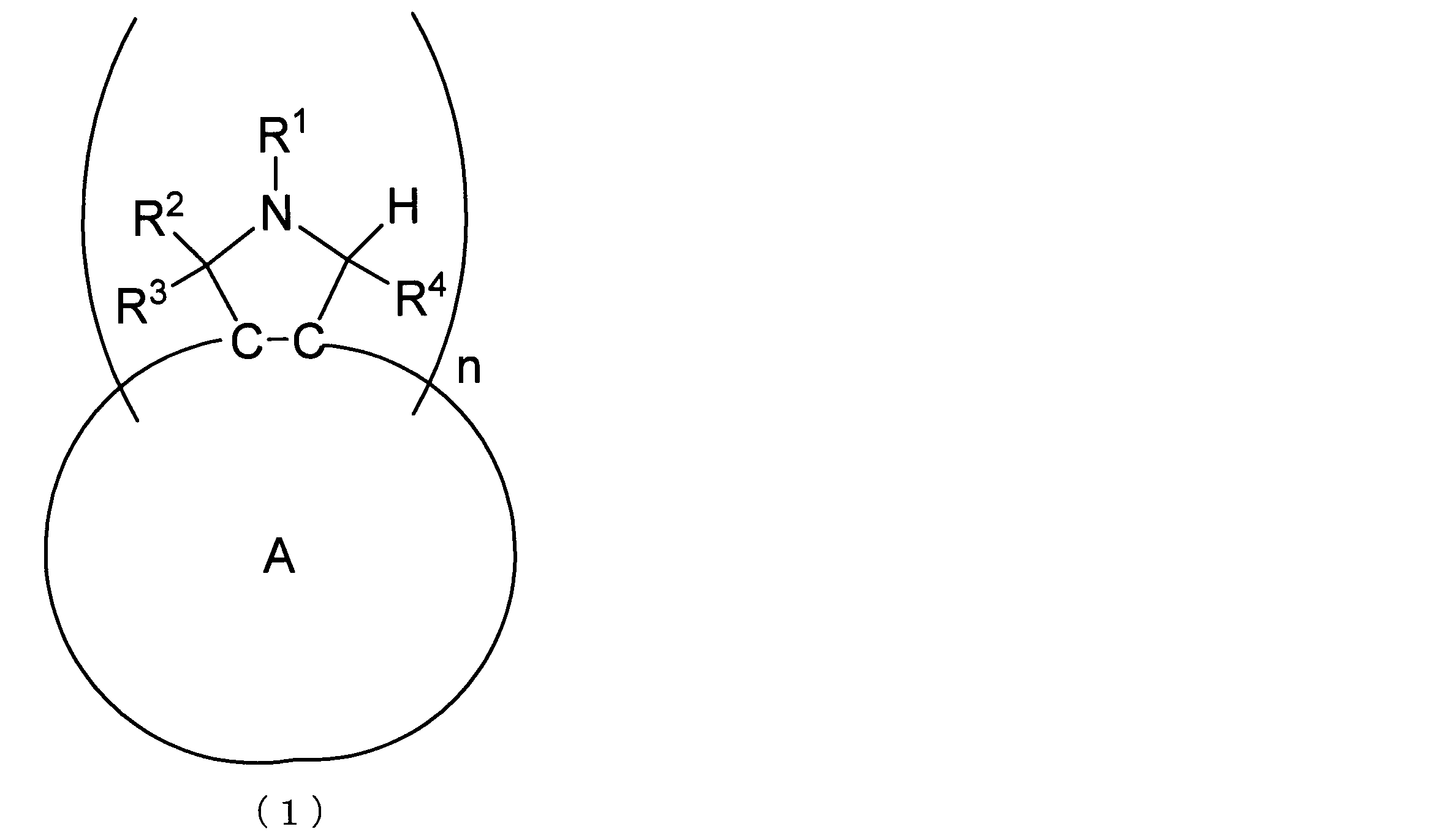
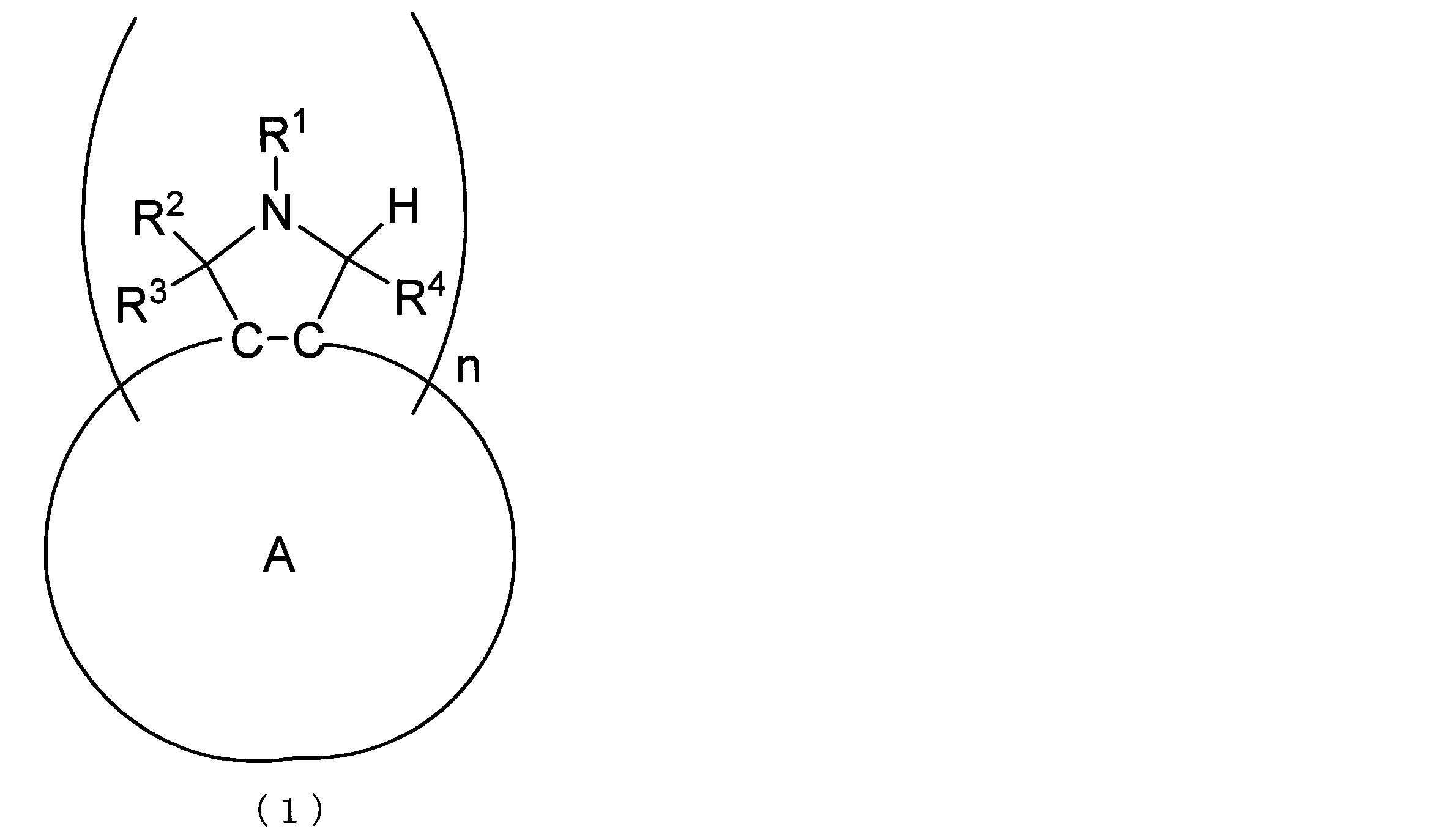
- a ring represents a fullerene skeleton.
- R 1 , R 2 , R 3 and R 4 each independently represent a hydrogen atom, a halogen atom, an alkyl group which may be substituted with a halogen atom, an aryl group which may have a substituent, or a substituent.
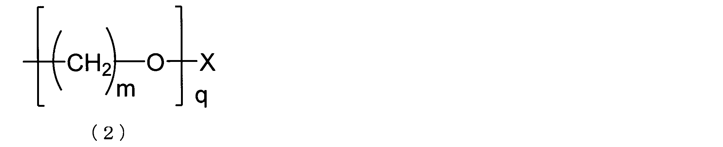
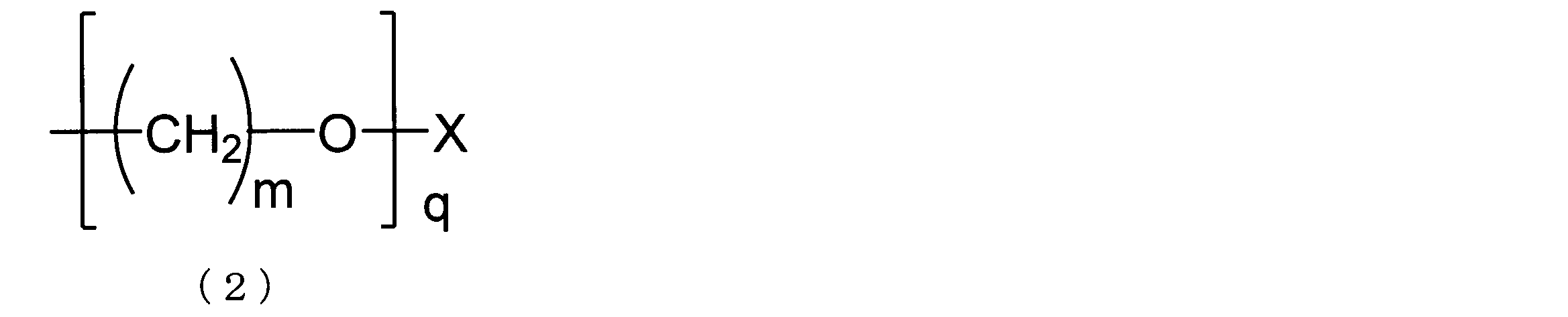
- monohydric heterocyclic group which may have a substituent, or group represented by following formula (2) is represented.
- n represents an integer of 1 or more.
- m represents an integer of 1 to 6.
- q represents an integer of 1 to 4.
- X represents a hydrogen atom, an alkyl group, or an aryl group which may have a substituent. When there are a plurality of m, the plurality of m may be the same or different.
- [2] The photoelectric conversion element according to [1], wherein R 1 is a group represented by the formula (2).
- Hole injection containing at least one selected from the group consisting of an aromatic amine compound and a polymer compound containing a repeating unit having an aromatic amine residue, provided between the anode and the active layer The photoelectric conversion element according to any one of [1] to [3], further including a layer.
- a solar cell module including the photoelectric conversion element according to any one of [1] to [4].
- An organic photosensor comprising the photoelectric conversion element according to any one of [1] to [4].
- the durability of the photoelectric conversion element against light irradiation can be further increased.
- the photoelectric conversion element of the present invention is provided between a cathode, an anode, the cathode and the anode, an active layer containing a perovskite compound, and provided between the cathode and the active layer.
- an electron transport layer containing a fullerene derivative represented by (1) is provided between a cathode, an anode, the cathode and the anode, an active layer containing a perovskite compound, and provided between the cathode and the active layer.
- an electron transport layer containing a fullerene derivative represented by (1) represented by (1).
- perovskite compound A perovskite compound is used as the material of the active layer of the photoelectric conversion element of the present invention.
- the perovskite compound refers to a compound having a perovskite structure.
- the perovskite compound is preferably a perovskite compound (perovskite compound having an organic-inorganic hybrid structure) in which an organic substance and an inorganic substance are constituent elements of the perovskite structure.
- the perovskite compound in the present invention is preferably a compound represented by the following formula (3), formula (4) or formula (5), more preferably a compound represented by the following formula (3). preferable.
- M 1 is a divalent metal (eg, Cu, Ni, Mn, Fe, Co, Pd, Ge, Sn, Pb, Eu), and the three X 1 are each independently , F, Cl, Br or I.
- CH 3 NH 3 PbI 3 , CH 3 NH 3 PbCl 3 , CH 3 NH 3 PbBr 3 , CH 3 NH 3 SnI 3 , CH 3 NH 3 SnCl 3 , CH 3 NH 3 SnBr 3 and the like are more preferable.
- R 10 is an alkyl group having 2 or more carbon atoms, an alkenyl group, an aralkyl group, an aryl group, a monovalent heterocyclic group or a monovalent aromatic heterocyclic group
- M 1 is Divalent metals (eg, Cu, Ni, Mn, Fe, Co, Pd, Ge, Sn, Pb, Eu), and four X 1 are each independently F, Cl, Br, or I. .
- M 1 is a divalent metal (eg, Cu, Ni, Mn, Fe, Co, Pd, Ge, Sn, Pb, Eu), and the three X 1 are independently , F, Cl, Br or I.
- the alkyl group represented by R 10 may be linear, branched, or a cycloalkyl group.
- the number of carbon atoms of the alkyl group represented by R 10 is usually 2 to 40, and preferably 2 to 30.
- Examples of the alkyl group represented by R 10 include an ethyl group, a propyl group, an isopropyl group, a tert-butyl group, a pentyl group, a hexyl group, an octyl group, an isooctyl group, a nonyl group, a dodecyl group, a tridecyl group, and a tetradecyl group.
- the number of carbon atoms in the alkenyl group represented by R 10 is usually 2 to 30, and preferably 2 to 20.
- Examples of the alkenyl group represented by R 10 include a vinyl group, 1-propenyl group, 2-propenyl group, 2-butenyl group, oleyl group, and allyl group.
- the number of carbon atoms in the aralkyl group represented by R 10 is usually 7 to 40, and preferably 7 to 30.
- Examples of the aralkyl group represented by R 10 include a benzyl group, a phenylethyl group, a phenylpropyl group, a naphthylmethyl group, and a naphthylethyl group.
- the number of carbon atoms of the aryl group represented by R 10 is usually 6 to 30, and preferably 6 to 20.
- Examples of the aryl group represented by R 10 include a phenyl group, p-chlorophenyl group, mesityl group, tolyl group, xylyl group, naphthyl group, anthryl group, azulenyl group, acenaphthenyl group, fluorenyl group, phenanthryl group, and indenyl group. , Pyrenyl group, biphenylyl group and the like.
- the monovalent heterocyclic group means a group obtained by removing one hydrogen atom bonded to the heterocyclic ring from the heterocyclic compound
- the monovalent aromatic heterocyclic group is A group obtained by removing one hydrogen atom bonded to an aromatic heterocyclic ring from an aromatic heterocyclic compound.
- the number of carbon atoms of the monovalent heterocyclic group represented by R 10 is usually 1 to 30, and preferably 1 to 20.
- the number of carbon atoms of the monovalent aromatic heterocyclic group represented by R 10 is usually 2 to 30, and preferably 2 to 20.
- Examples of the monovalent heterocyclic group or monovalent aromatic heterocyclic group represented by R 10 include pyrrolidyl group, imidazolidinyl group, morpholyl group, oxazolyl group, oxazolidinyl group, furyl group, thienyl group, pyridyl group, Examples include pyridazinyl group, pyrimidinyl group, pyrazinyl group, triazinyl group, imidazolyl group, pyrazolyl group, thiazolyl group, quinazolinyl group, carbazolyl group, carbolinyl group, diazacarbazolyl group, and phthalazinyl group.
- perovskite compound Only one perovskite compound may be used as the active layer material, or two or more perovskite compounds may be used.
- a ring represents a fullerene skeleton.
- R 1 , R 2 , R 3 and R 4 each independently represent a hydrogen atom, a halogen atom, an alkyl group which may be substituted with a halogen atom, an aryl group which may have a substituent, or a substituent.
- monohydric heterocyclic group which may have a substituent, or group represented by following formula (2) is represented.
- n represents an integer of 1 or more.
- m represents an integer of 1 to 6.
- q represents an integer of 1 to 4.
- X represents a hydrogen atom, an alkyl group, or an aryl group which may have a substituent.
- the plurality of m may be the same as or different from each other.
- n is preferably 1 or 2.
- m is preferably 2.
- q is preferably 2.
- the alkyl group represented by X usually has 1 to 30 carbon atoms, and preferably 1 to 20 carbon atoms.
- the number of carbon atoms of the aryl group in the “aryl group optionally having substituent (s)” represented by X is usually 6-30, and preferably 6-20.
- X is preferably a hydrogen atom or an alkyl group, more preferably a hydrogen atom or an alkyl group having 1 to 5 carbon atoms, and even more preferably a hydrogen atom or a methyl group.
- R 1 is preferably a group represented by the formula (2).
- “which may have a substituent” means that all hydrogen atoms constituting the compound or group are unsubstituted and a part or all of one or more hydrogen atoms. Including both embodiments where is substituted by a substituent.
- substituents examples include an alkyl group, a halogenated alkyl group, an alkoxy group, an alkylthio group, an aryl group, an aryloxy group, an arylthio group, an arylalkyl group, an arylalkoxy group, an arylalkylthio group, an arylalkenyl group, and an arylalkynyl group.
- Amino group substituted amino group, silyl group, substituted silyl group, silyloxy group, substituted silyloxy group, halogen atom, acyl group, acyloxy group, imine residue, dialkylamino group, diarylamino group, amide group, acid imide group, Examples thereof include a monovalent heterocyclic group, a carboxyl group, a substituted carboxyl group, a cyano group, and a polymerizable substituent.
- the “polymerizable substituent” means a substituent capable of forming a compound by forming a bond between two or more molecules by causing a polymerization reaction.
- Examples of such a group include a group having a carbon-carbon multiple bond (for example, a vinyl group, an ethynyl group, a butenyl group, an acryloyl group, a group in which one hydrogen atom is removed from an acrylate ester, and one hydrogen atom from acrylamide.
- combinations of groups capable of forming an ester bond or an amide bond can also be used.
- groups of groups capable of forming an ester bond or an amide bond include a combination of a hydrocarbyloxycarbonyl group and an amino group, a combination of a hydrocarbyloxycarbonyl group and a hydroxy group, and the like.
- Examples of the fullerene skeleton represented by the A ring include a fullerene skeleton derived from C 60 fullerene and a fullerene skeleton derived from fullerene having 70 or more carbon atoms.
- the fullerene skeleton represented by the A ring may be a fullerene skeleton to which a predetermined group is added.
- the fullerene skeleton represented by the A ring has a plurality of groups, the plurality of groups may be bonded to each other.
- the group that the fullerene skeleton represented by the A ring may have include an indan-1,3-diyl group and a methylene group that may have a substituent.
- Preferred examples of the substituent in the “optionally substituted methylene group” that the fullerene skeleton represented by the A ring may have include an aryl group, a heteroaryl group, and a hydrocarbyloxycarbonylalkyl group. It is done.
- the “optionally substituted methylene group” that the fullerene skeleton represented by the A ring may have, a methylene group having an aryl group and a hydrocarbyloxycarbonylalkyl group is preferable, and a phenyl group and an alkoxycarbonylpropyl A methylene group having a group is more preferable, and a methylene group having a phenyl group and a methoxycarbonylpropyl group is further preferable.
- the fullerene skeleton represented by the A ring may be a fullerene skeleton derived from phenyl C61 butyric acid methyl ester (C60PCBM) or a fullerene skeleton derived from phenyl C71 butyric acid methyl ester (C70PCBM).
- Examples of the halogen atom represented by R 1 , R 2 , R 3, and R 4 include a fluorine atom, a chlorine atom, a bromine atom, and an iodine atom.
- the alkyl group in the “alkyl group optionally substituted with a halogen atom” represented by R 1 , R 2 , R 3 and R 4 may be linear or branched, and cycloalkyl It may be a group.
- the number of carbon atoms of the “alkyl group optionally substituted with a halogen atom” represented by R 1 , R 2 , R 3 and R 4 is usually from 1 to 30, and preferably from 1 to 20.
- R 1, R 2, R 3 and halogen atoms in the "alkyl group optionally substituted with a halogen atom" represented by R 4 is represented by R 1, R 2, R 3 and R 4 This is the same as the example of the halogen atom.
- the aryl group in the “aryl group optionally having substituent (s)” represented by R 1 , R 2 , R 3 and R 4 represents one hydrogen atom bonded to the aromatic ring from the aromatic hydrocarbon. It means the group removed.
- the number of carbon atoms of the aryl group is usually 6 to 60, preferably 6 to 16, and more preferably 6 to 10.
- the aryl group include a phenyl group, a 1-naphthyl group, and a 2-naphthyl group.
- the hydrogen atom in the aryl group may be substituted with a substituent.
- the substituent include an alkyl group, a halogen atom, a halogenated alkyl group, an alkoxy group, a dialkylamino group, a diarylamino group, a silyl group, And substituted silyl groups.
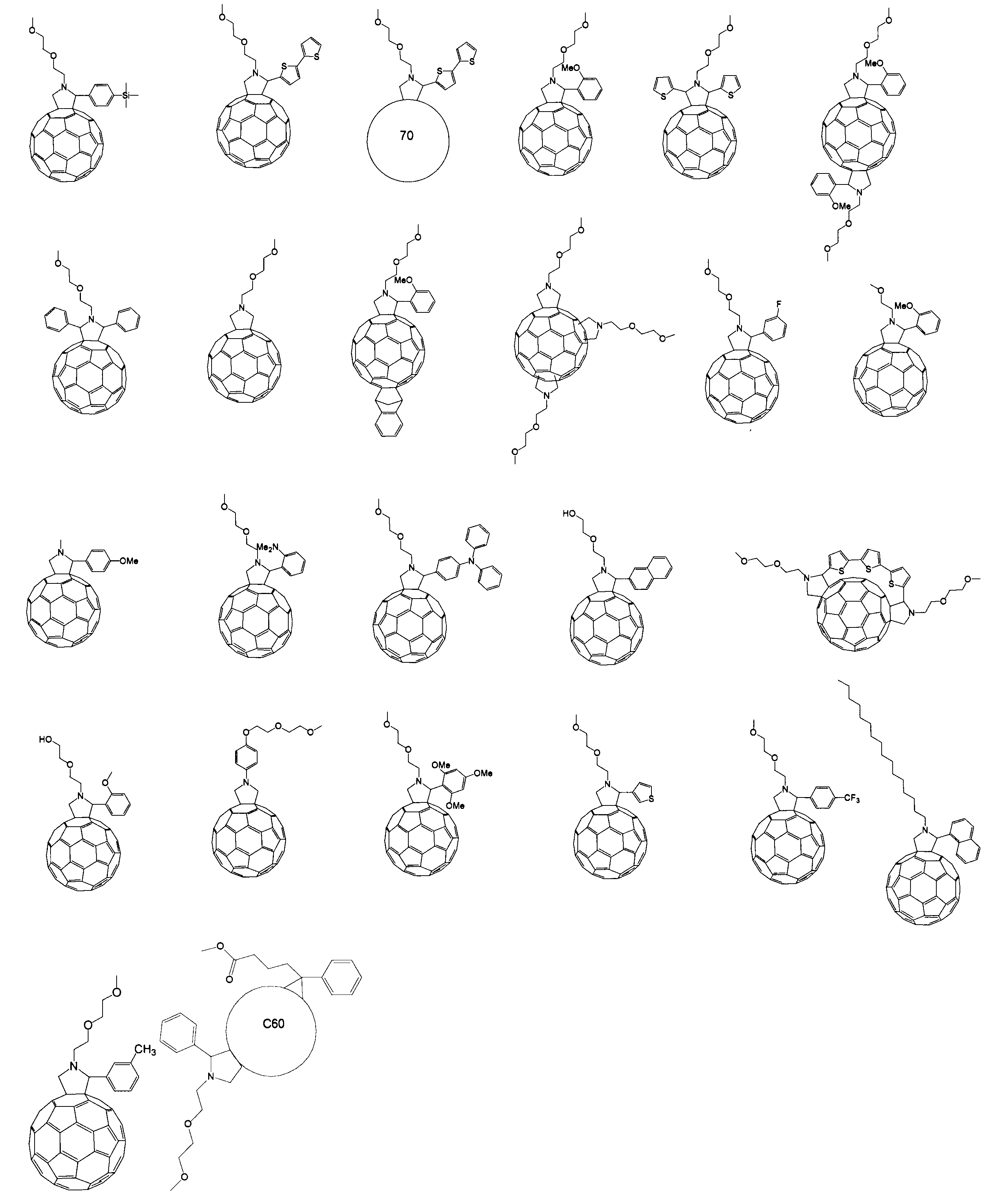
- aryl group having a substituent examples include, for example, 3-methylphenyl group, trimethylsilylphenyl group, 2-methoxyphenyl group, 4-methoxyphenyl group, 2,4,5-trimethoxyphenyl group, 4- (diphenylamino) -Phenyl group, 2- (dimethylamino) -phenyl group, 3-fluorophenyl group, and 4- (trifluoromethyl) -phenyl group.
- the number of carbon atoms of the arylalkyl group in the “arylalkyl group optionally having substituent (s)” represented by R 1 , R 2 , R 3 and R 4 is usually from 7 to 61, and from 7 to 17 Preferably, it is preferably 7 to 11.
- Specific examples of the arylalkyl group include benzyl group, phenylethyl group, phenylpropyl group, naphthylmethyl group, naphthylethyl group and the like.
- the number of carbon atoms of the monovalent heterocyclic group in the “monovalent heterocyclic group optionally having substituent (s)” represented by R 1 , R 2 , R 3 and R 4 is usually 1-30. Yes, it is preferably 1-20.
- Examples of the monovalent heterocyclic group in the “monovalent heterocyclic group optionally having a substituent” represented by R 1 , R 2 , R 3 and R 4 include a thienyl group, 2,2 A '-bithiophen-5-yl group is mentioned.
- the plurality of R 4 may be bonded to each other.
- examples of the substituent to which a plurality of R 4 groups are bonded include a divalent group represented by the following formula (3). Can be mentioned.
- p represents an integer of 1 to 5. p is preferably an integer of 2 to 4, and more preferably 3.
- the divalent group represented by the above formula (3) may have a substituent.
- fullerene derivative represented by the formula (3) include the following structures.
- the ring structures with numerical values “60” and “70” in the following structures represent a C 60 fullerene skeleton and a C 70 fullerene skeleton, respectively.
- the fullerene derivative represented by the formula (1) described above can be produced by any conventionally known suitable method.
- the fullerene derivative represented by the formula (1) is obtained by, for example, a method using a 1,3-dipolar cycloaddition reaction between an iminium cation generated by decarboxylation from an imine formed from a glycine derivative and an aldehyde, and fullerene. Can be manufactured. Such methods are disclosed in, for example, Japanese Patent Application Laid-Open Nos. 2009-67708, 2009-84264, 2011-241205, and 2011-77486.
- the reaction conditions such as reaction time and reaction temperature, and the amount of reaction raw materials (for example, glycine derivative, aldehyde, and fullerene) used,
- the number of “n” in the fullerene derivative represented by the formula (1) can be adjusted.
- Photoelectric conversion element The cathode, anode, active layer, and electron transport layer included in the photoelectric conversion element of the present invention and other elements (hole injection layer and the like) included as necessary will be described in detail below.
- the photoelectric conversion element of the present invention includes a pair of electrodes (an anode and a cathode) and an active layer provided between the pair of electrodes.
- An electron transport layer is provided between the cathode and the active layer.
- the photoelectric conversion element of the present invention is usually produced on a support substrate.
- a substrate made of a material that does not change chemically when an electrode is formed and an organic layer is formed to produce a photoelectric conversion element is preferably used.
- the material for the support substrate include glass, plastic, polymer film, and silicon.
- a substrate having high light transmittance is preferably used as the support substrate.
- the electrode far from the support substrate is transparent or translucent. Since the electrode far from the support substrate is transparent or translucent, when an opaque support substrate is used, light can be taken in through the electrode far from the support substrate.
- the electrode is formed of a conductive material.
- a material for the electrode for example, an organic substance such as a metal, a metal oxide, or a conductive polymer can be used.
- the electrode material include lithium, sodium, potassium, rubidium, cesium, magnesium, calcium, strontium, barium, aluminum, scandium, vanadium, zinc, yttrium, indium, cerium, samarium, europium, terbium, ytterbium, gold, Silver, platinum, copper, manganese, titanium, cobalt, nickel, tungsten, tin and other metals, alloys containing two or more metals selected from the group consisting of these metals, indium oxide, zinc oxide, tin oxide, ITO, Examples thereof include fluorinated tin oxide (FTO), indium zinc oxide (IZO), graphite, and a graphite intercalation compound.
- FTO fluorinated tin oxide
- IZO indium zinc oxide
- graphite graph
- the alloy examples include magnesium-silver alloy, magnesium-indium alloy, magnesium-aluminum alloy, indium-silver alloy, lithium-aluminum alloy, lithium-magnesium alloy, lithium-indium alloy, calcium-aluminum alloy and the like.
- the conductive polymer examples include polyaniline and its derivatives, polythiophene and its derivatives.
- the electrode may be in the form of a single layer or in the form of a plurality of layers stacked.
- the perovskite compound contained in the active layer of the photoelectric conversion element of the present invention usually has a crystal structure, and light incident from the transparent or translucent electrode side is absorbed by the perovskite compound having a crystal structure in the active layer. To generate electrons and holes. The generated electrons and holes move in the active layer and reach different electrodes, and are extracted as electric energy (current) outside the photoelectric conversion element.
- transparent or translucent electrode materials include conductive metal oxides, metals, etc. If these materials are not transparent, they should be thin enough to transmit light. Thus, a transparent or translucent electrode can be obtained.
- the transparent or translucent electrode material include, for example, indium oxide, zinc oxide, tin oxide, and composites thereof such as ITO, IZO, FTO, NESA, gold, platinum, silver, copper, and aluminum. Is mentioned.
- the material of the transparent or translucent electrode preferably contains one or more selected from ITO, IZO and tin oxide, and more preferably one or more selected from ITO, IZO and tin oxide.
- the surface of the electrode may be subjected to treatments such as ozone UV treatment, corona treatment, and ultrasonic treatment.
- the electrode material is formed on a layer on which the electrode is to be formed or a support substrate by vacuum deposition, sputtering, ion plating, plating, coating, or the like. be able to.
- the electrode material is polyaniline and its derivatives, polythiophene and its derivatives, nanoparticles, nanowires or emulsions (suspensions) or suspensions containing nanotubes
- the electrode is preferably formed by a coating method. be able to.
- the electrode may be formed by a coating method using a coating liquid containing the conductive substance, a metal ink, a metal paste, a low-melting-point metal in a molten state, or the like.
- a coating liquid containing the conductive substance, a metal ink, a metal paste, a low-melting-point metal in a molten state, or the like.
- methods for applying the coating liquid include spin coating, casting, micro gravure coating, gravure coating, bar coating, roll coating, wire bar coating, dip coating, and spray coating. , Screen printing method, flexographic printing method, offset printing method, inkjet printing method, dispenser printing method, nozzle coating method, capillary coating method, among these, spin coating method, flexographic printing method, inkjet printing method, dispenser A printing method is preferred.
- Examples of the conductive substance that can be contained in the above emulsion or suspension include metals such as gold and silver, oxides such as ITO, and carbon nanotubes.
- the electrode may be composed only of nanoparticles or nanofibers.
- nanoparticles or nanofibers may be dispersed in a predetermined medium such as a conductive polymer.
- Examples of the solvent of the coating solution used when forming the electrode by a coating method include hydrocarbon solvents such as toluene, xylene, mesitylene, tetralin, decalin, bicyclohexyl, n-butylbenzene, sec-butylbesen, and tert-butylbenzene.
- hydrocarbon solvents such as toluene, xylene, mesitylene, tetralin, decalin, bicyclohexyl, n-butylbenzene, sec-butylbesen, and tert-butylbenzene.
- Halogenated saturated hydrocarbon solvents such as carbon tetrachloride, chloroform, dichloromethane, dichloroethane, chlorobutane, bromobutane, chloropentane, bromopentane, chlorohexane, bromohexane, chlorocyclohexane, bromocyclohexane, chlorobenzene, dichlorobenzene, trichlorobenzene, etc.
- Examples include halogenated unsaturated hydrocarbon solvents, ether solvents such as tetrahydrofuran and tetrahydropyran, water, and alcohols.
- the alcohol examples include methanol, ethanol, isopropanol, butanol, ethylene glycol, propylene glycol, butoxyethanol, methoxybutanol and the like.
- the coating liquid used for this invention may contain 2 or more types of solvent, and may contain 2 or more types of solvent illustrated above.
- the active layer is a layer having a function of converting light energy into electric energy.
- the active layer of the photoelectric conversion element of the present invention contains a perovskite compound. Specific examples and preferred examples of the perovskite compound are as described above.
- the active layer may contain other components in addition to the perovskite compound.
- other components that can be included in the active layer include an electron-donating compound, an electron-accepting compound, an ultraviolet absorber, an antioxidant, and a sensitizer for sensitizing the function of generating charge by absorbed light, Examples thereof include a light stabilizer for increasing stability to ultraviolet light and a binder for enhancing mechanical properties.
- the method for forming the active layer containing the perovskite compound is not particularly limited.
- Examples of the method for forming the active layer include a coating method. From the viewpoint of simplifying the process of forming the active layer, it is preferable to form an active layer containing a perovskite compound by a coating method.
- the coating solution that can be used in the coating method may be a solution containing the perovskite compound or a solution containing a precursor that can be converted into a perovskite compound by a self-organization reaction after the formation of the layer.
- Examples of such a precursor include CH 3 NH 3 PbI 3 , CH 3 NH 3 PbBr 3 , (CH 3 (CH 2 ) n CHCH 3 NH 3 ) 2 PbI 4 (where n is an integer of 5 to 8) in a.) include (C 6 H 5 C 2 H 4 NH 3) 2 PbBr 4.
- the active layer containing the perovskite compound represented by the above formulas (3) to (5) is formed by applying a solution containing a metal halide on the layer on which the active layer is to be formed, A method of further applying a solution containing an ammonium halide, a solution containing an amine halide or a formamidine hydrohalide to a halide film, or a solution containing an ammonium halide formed from a formed metal halide film, It can also be formed by a method of immersing in a solution containing a halogenated amine or formamidine hydrohalide.
- a solution containing lead iodide is applied on the layer on which the active layer is to be formed, and a solution containing methylammonium iodide is applied to the formed lead iodide film.
- a solution containing methylammonium iodide is applied to the formed lead iodide film.
- Examples of the method for applying the coating solution containing the perovskite compound, the solution containing the metal halide, the solution containing the ammonium halide, and the solution containing the halogenated amine include spin coating, casting, and microgravure coating. Method, gravure coating method, bar coating method, roll coating method, wire bar coating method, dip coating method, spray coating method, screen printing method, flexographic printing method, offset printing method, inkjet printing method, dispenser printing method, nozzle coating method And a capillary coating method. Among these, a spin coating method, a flexographic printing method, an ink jet printing method, and a dispenser printing method are preferable.
- the coating solution used for the coating method may contain a solvent in addition to the perovskite compound or a precursor of the perovskite compound, and the solvent is contained. It is preferable.
- esters eg, methyl formate, ethyl formate, propyl formate, pentyl formate, methyl acetate, ethyl acetate, pentyl acetate, etc.
- Ketones eg, ⁇ -butyrolactone, N-methyl-2-pyrrolidone, acetone, dimethyl ketone, diisobutyl ketone, cyclopentanone, cyclohexanone, methylcyclohexanone, etc.
- ethers eg, diethyl ether, methyl-tert-butyl ether
- Diisopropyl ether dimethoxymethane, dimethoxyethane, 1,4-dioxane, 1,3-dioxolane, 4-methyldioxolane, tetrahydrofuran, methyltetrahydrofuran, anisole,
- the compounds constituting these solvents may have a branched structure or a cyclic structure, and are functional groups of esters, ketones, ethers and alcohols (that is, groups represented by —O—, — (C Or a group represented by —OO—, a group represented by —COO—, or a group represented by —OH).
- the hydrogen atom in the hydrocarbon moiety of the esters, ketones, ethers and alcohols may be substituted with a halogen atom (particularly a fluorine atom).
- the coating liquid for forming the said active layer may contain 2 or more types of solvent, and may contain 2 or more types of solvent illustrated above.
- the amount of solvent used in the coating solution is preferably 1 to 10,000 times the weight of the perovskite compound or the perovskite compound precursor, and more preferably 10 to 1000 times the weight.
- the weight of the solvent is preferably 1 to 10,000 times, and more preferably 10 to 1,000 times the weight of the metal halide, ammonium halide, and amine halide. .
- the coating liquid is not limited to this, and may be a solution or a solution, and may be a dispersion such as an emulsion (emulsion) or a suspension (suspension).
- the solvent After the application of the coating liquid, it is preferable to remove the solvent in forming the active layer.
- the method for removing the solvent include heat treatment, air drying treatment, and decompression treatment.
- an electron transport layer is provided between the cathode and the active layer.
- the electron transport layer contains a fullerene derivative represented by the above formula (1). Specific examples and preferred examples of the fullerene derivative represented by the formula (1) are as described above.
- the electron transport layer may contain an electron transport material other than the fullerene derivative represented by the formula (1).
- the electron transporting material that may be contained in the electron transport layer other than the fullerene derivative represented by the formula (1) may be an organic compound or an inorganic compound.
- Examples of the electron-transporting material that is an organic compound include an electron-transporting material that is a low-molecular compound and an electron-transporting material that are high-molecular compounds exemplified below, and carbon nanotubes.
- the electron transport material which is a polymer compound include polyvinyl carbazole and derivatives thereof, polysilane and derivatives thereof, polysiloxane derivatives containing an aromatic amine structure in the side chain or main chain, polyaniline and derivatives thereof, polythiophene and derivatives thereof.
- the fullerene and derivatives thereof e.g., C 60 fullerene, C 70 fullerene, and C 70 fullerene is greater carbon atoms than the fullerene, and derivatives thereof.
- Examples of the C 60 fullerene derivative include the following fullerene derivatives.
- Examples of the electron transport material that is an inorganic compound include zinc oxide, titanium oxide, zirconium oxide, tin oxide, indium oxide, ITO, FTO, gallium-doped zinc oxide (GZO), antimony-doped tin oxide (ATO), and aluminum.
- Doped zinc oxide (AZO) is mentioned, Among these, zinc oxide, gallium doped zinc oxide or aluminum doped zinc oxide is preferable.
- an electron transport layer containing an electron transport material that is an inorganic compound in addition to the fullerene derivative represented by the formula (1), it is preferable to form an electron transport layer by making an inorganic compound into a particulate form and making it contain in a coating liquid, and apply
- an electron transporting material containing a particulate inorganic compound an electron transporting material containing nanoparticles of zinc oxide, gallium-doped zinc oxide or aluminum-doped zinc oxide is preferable. It is preferable that the electron transport material which is an inorganic compound consists only of nanoparticles of zinc oxide, gallium-doped zinc oxide or aluminum-doped zinc oxide.
- the average particle diameter corresponding to the spheres of zinc oxide, gallium-doped zinc oxide or aluminum-doped zinc oxide is preferably 1 nm to 1000 nm, and more preferably 10 nm to 100 nm.
- the average particle diameter can be measured by a laser light scattering method or an X-ray diffraction method.
- the electron transport layer is preferably formed by a coating method.
- the coating solution used when forming the electron transport layer by a coating method may contain other electron transport materials as necessary.
- the electron transport layer is preferably formed by applying a coating solution containing a fullerene derivative represented by the formula (1), another electron transport material added as necessary, and a solvent to the active layer. .
- the coating solution it is preferable to use a coating solution that does not damage or hardly gives a layer (active layer or the like) to which the coating solution is applied. Specifically, a layer (active layer or the like) to which the coating solution is applied is used. It is preferable that the coating solution does not dissolve or hardly dissolves.
- Examples of the solvent contained in the coating solution for forming the electron transport layer include alcohols, ketones, and hydrocarbons.
- the alcohol include methanol, ethanol, isopropanol, butanol, ethylene glycol, propylene glycol, butoxyethanol, methoxybutanol and the like.
- Specific examples of ketones include acetone, methyl ethyl ketone, methyl isobutyl ketone, 2-heptanone, cyclohexanone and the like.
- Specific examples of hydrocarbons include n-pentane, cyclohexane, n-hexane, benzene, toluene, xylene, tetralin.
- the coating liquid for forming an electron carrying layer may contain 2 or more types of solvent, and may contain 2 or more types of solvent illustrated above.
- the amount of the solvent used is preferably 1 to 10,000 times the weight of the fullerene derivative represented by the formula (1) and the other electron transporting material added as necessary. The weight is more preferably 10 times or more and 1000 times or less.
- the coating solution containing the solvent, the fullerene derivative represented by the formula (1), and another electron transporting material as necessary is preferably used after filtration, and a fluorine-containing resin having a pore size of 0.5 ⁇ m. It is preferable to filter using a filter (for example, Teflon (registered trademark)).
- the solvent In forming the electron transport layer by applying the coating solution, it is preferable to remove the solvent.
- the method for removing the solvent include the same method as the method for removing the solvent described in the method for forming the active layer.
- an active layer may be provided between the cathode and the anode, and an electron transport layer may be provided between the cathode and the active layer.
- the cathode, the electron transport layer, the active layer Even if it is provided in the order of the anode, it may be provided on the substrate in the order of the anode, the active layer, the electron transport layer, and the cathode.
- the photoelectric conversion element of the present invention is preferably a photoelectric conversion element further including a support substrate, wherein the support substrate, the anode, the active layer, the electron transport layer, and the cathode are provided in this order.
- the photoelectric conversion element of the present invention may include other arbitrary layers exhibiting various functions in addition to the above-described active layer and electron transport layer.
- Examples of other optional layers include a hole injection layer and a hole transport layer.
- the photoelectric conversion element of the present invention is provided between the anode and the active layer, and includes at least one selected from the group consisting of an aromatic amine compound and a polymer compound containing a repeating unit having an aromatic amine residue.
- a hole injection layer may be further included.
- the hole injection layer is provided between the anode and the active layer and has a function of promoting hole injection into the anode.
- the hole injection layer is preferably provided in contact with the anode.
- a material for the hole injection layer a material capable of making the formed hole injection layer insoluble in water is preferable.
- the material capable of making the formed hole injection layer insoluble in water may be either an organic material or an inorganic material.
- two or more materials that can make the formed hole injection layer insoluble in water may be used in combination.
- materials that can make the formed hole injection layer insoluble in water include polyaniline and derivatives thereof, polythiophene and derivatives thereof, polypyrrole and derivatives thereof, and a polymer including a repeating unit having an aromatic amine residue.
- examples include high molecular compounds such as compounds, low molecular compounds such as aniline, thiophene, pyrrole, and aromatic amine compounds, and inorganic compounds such as CuSCN and CuI.
- the material capable of making the formed hole injection layer insoluble in water is selected from the group consisting of polythiophene and derivatives thereof, aromatic amine compounds, polymer compounds containing repeating units having an aromatic amine residue, CuSCN, and CuI. One or more selected are preferable.
- the material capable of making the formed hole injection layer insoluble in water is an aromatic amine compound or a polymer compound containing a repeating unit having an aromatic amine residue. It is preferable that it is 1 or more types chosen from the group which consists of.
- the polymer compound, which is a material that can make the formed hole injection layer insoluble in water includes a repeating unit having an aromatic amine residue from the viewpoint of extending the lifetime of the photoelectric conversion element. High molecular compounds are more preferred.
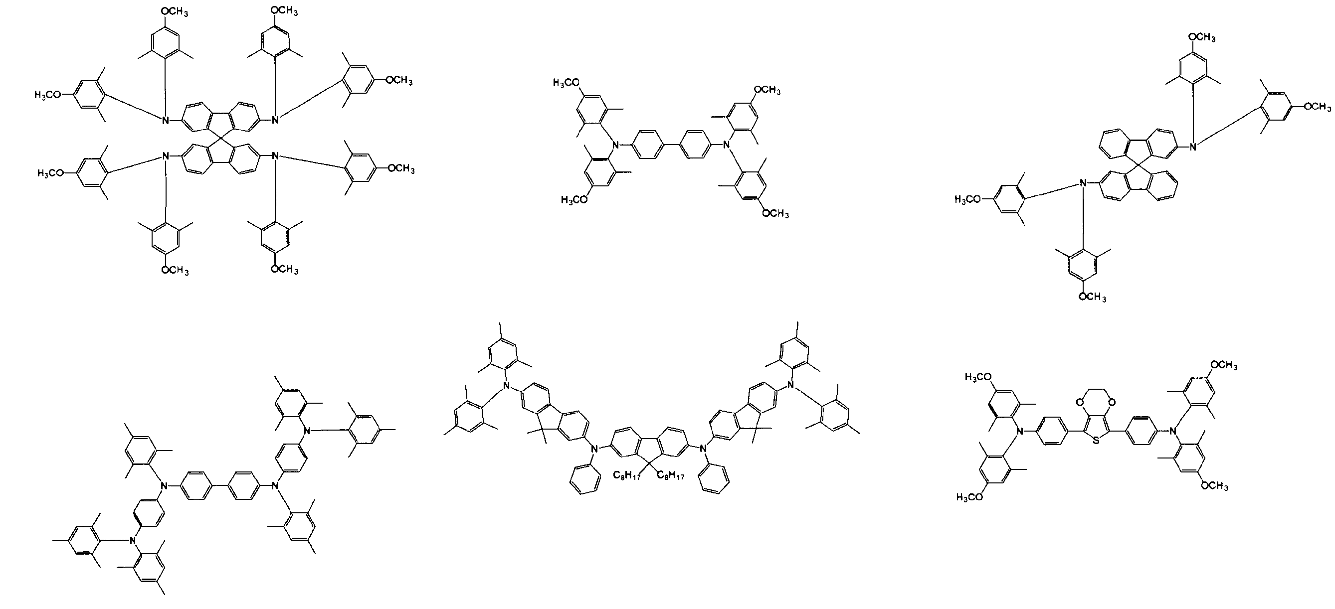
- aromatic amine compound examples include compounds represented by the following formula.
- the aromatic amine compound preferably contains a phenyl group having at least three substituents.
- Examples of the substituent that the phenyl group contained in the aromatic amine compound may have include an alkyl group, an alkoxy group, an amino group, and a silyl group.
- aromatic amine compound containing a phenyl group having at least three substituents include compounds represented by the following formula.
- the repeating unit having an aromatic amine residue is a repeating unit obtained by removing two hydrogen atoms from the aromatic amine compound.
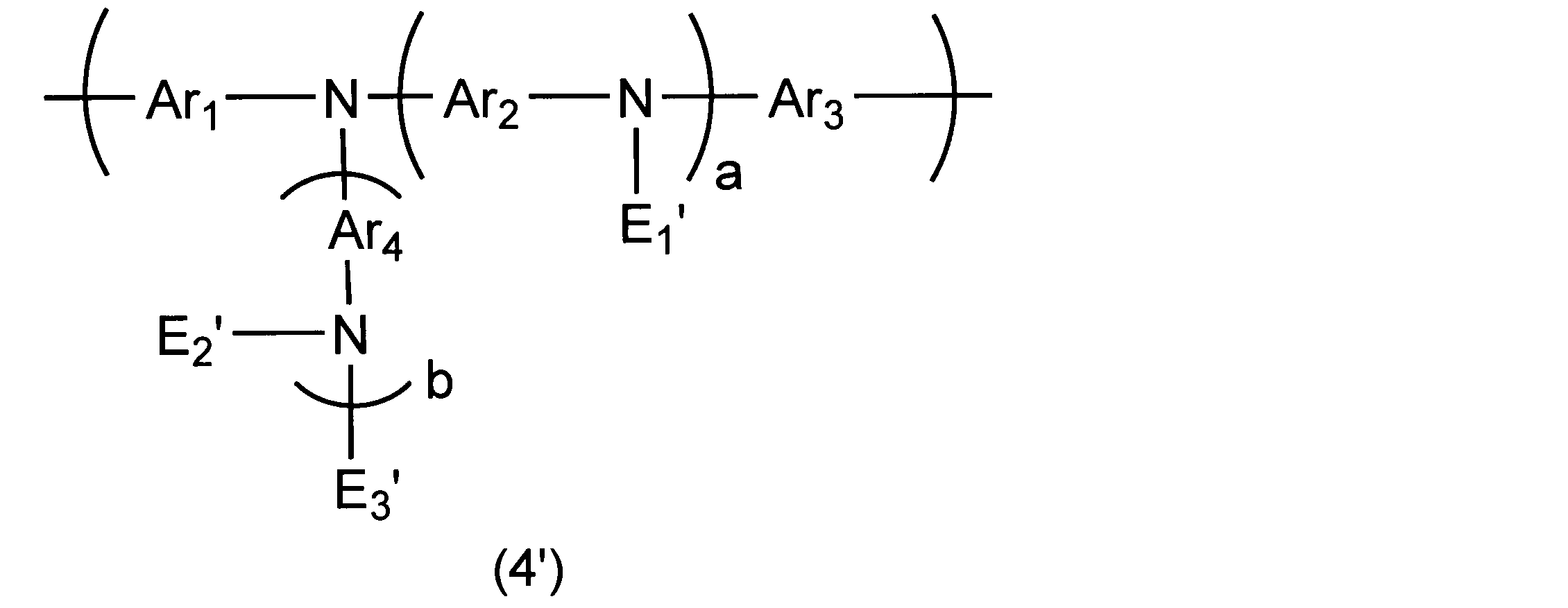
- the repeating unit having an aromatic amine residue include a repeating unit represented by the following formula (4 ′).
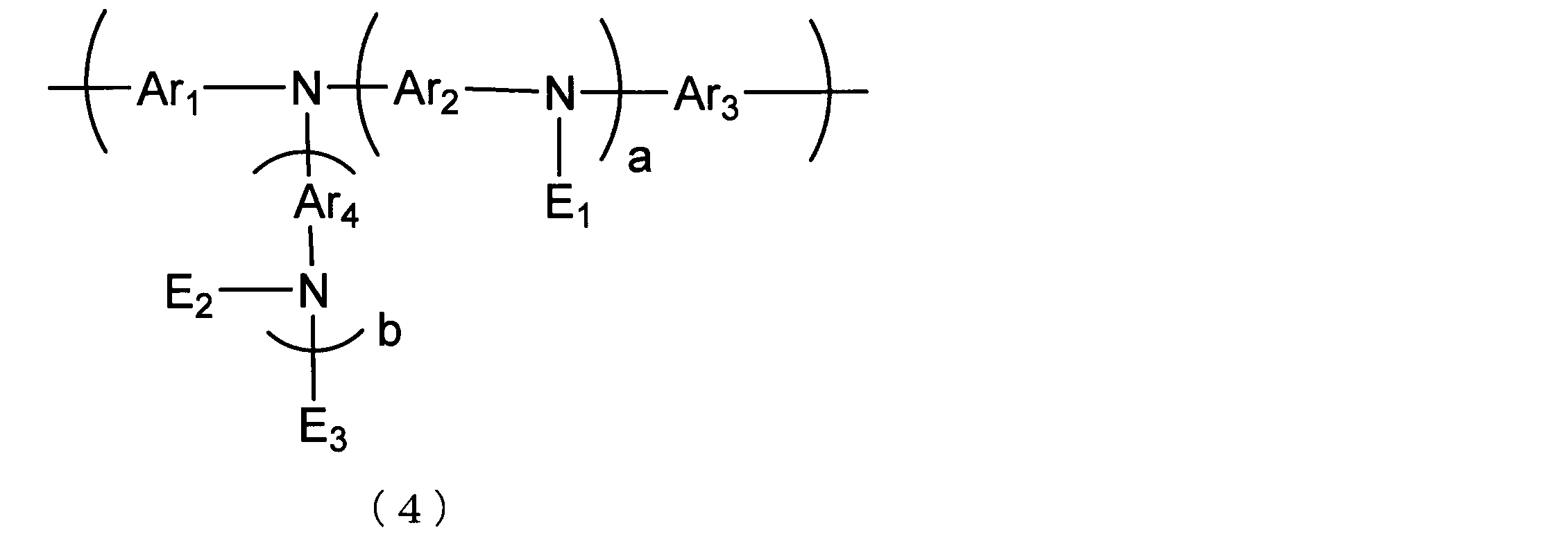
- the repeating unit represented by the following formula (4 ′) is preferably a repeating unit represented by the following formula (4).
- the polymer compound containing a repeating unit having an aromatic amine residue preferably contains a phenyl group having at least three substituents.
- Ar 1 , Ar 2 , Ar 3 and Ar 4 each independently represent an arylene group (A1) or a divalent heterocyclic group (B1).
- E 1 ′, E 2 ′ and E 3 ′ each independently represent an aryl group (A2 ′) or a monovalent heterocyclic group (B2 ′).
- a and b each independently represent 0 or 1, and 0 ⁇ a + b ⁇ 1.
- Arylene group (A1) The arylene group (A1) is an atomic group obtained by removing two hydrogen atoms from an aromatic hydrocarbon, a divalent group having a benzene ring or a condensed ring, and an independent benzene ring or condensed. A divalent group in which two or more rings are bonded directly or via a vinylene group is also included.
- the arylene group (A1) may have a substituent.
- Examples of the substituent that the arylene group (A1) may have include an alkyl group, an alkoxy group, an alkylthio group, an aryl group, an aryloxy group, an arylthio group, an arylalkyl group, an arylalkoxy group, an arylalkylthio group, and an arylalkenyl group.
- Arylalkynyl group amino group, substituted amino group, silyl group, substituted silyl group, silyloxy group, substituted silyloxy group, halogen atom, acyl group, acyloxy group, imine residue, amide group, acid imide group, monovalent complex
- a cyclic group a carboxyl group, a substituted carboxyl group, a cyano group, and the like.
- the heterocyclic group is preferably.
- the number of carbon atoms of the arylene group having no substituent is usually about 6 to 60, and preferably 6 to 20.
- Divalent heterocyclic group (B1) is the remaining atomic group obtained by removing two hydrogen atoms from the heterocyclic compound, and the divalent heterocyclic group (B1) is It may have a substituent.
- the heterocyclic compound is an organic compound having a cyclic structure, and the elements constituting the ring are not only carbon atoms, but also oxygen atoms, sulfur atoms, nitrogen atoms, phosphorus atoms, boron atoms, arsenic atoms, etc. A compound containing a hetero atom in the ring.
- Examples of the substituent that the divalent heterocyclic group (B1) may have include an alkyl group, an alkoxy group, an alkylthio group, an aryl group, an aryloxy group, an arylthio group, an arylalkyl group, an arylalkoxy group, and an arylalkylthio group.
- the number of carbon atoms of the divalent heterocyclic group having no substituent is usually about 3 to 60.
- Aryl group (A2 ′) may have a substituent.
- substituents that the aryl group (A2 ′) may have include an alkyl group, an alkoxy group, an alkylthio group, an aryl group, an aryloxy group, an arylthio group, an arylalkyl group, an arylalkoxy group, an arylalkylthio group, and an arylalkenyl group.
- the number of carbon atoms in the aryl group having no substituent is usually about 6 to 30, preferably 6 to 20.
- the monovalent heterocyclic group (B2 ′) may have a substituent.
- substituents that the monovalent heterocyclic group (B2 ′) may have include an alkyl group, an alkoxy group, an alkylthio group, an aryl group, an aryloxy group, an arylthio group, an arylalkyl group, an arylalkoxy group, and an arylalkylthio group.
- the number of carbon atoms of a monovalent heterocyclic group having no substituent is usually about 1 to 30.
- Ar 1 , Ar 2 , Ar 3 and Ar 4 represent the same meaning as described above.
- E 1 , E 2 and E 3 each independently represent an aryl group (A2) or a monovalent heterocyclic group (B2) defined as follows.
- A2 aryl group
- B2 monovalent heterocyclic group
- Arylene group (A1) The arylene group (A1) is an atomic group obtained by removing two hydrogen atoms from an aromatic hydrocarbon, a divalent group having a benzene ring or a condensed ring, and an independent benzene ring or condensed. A divalent group in which two or more rings are bonded directly or via a vinylene group is also included.
- the arylene group (A1) may have a substituent.
- Examples of the substituent that the arylene group (A1) may have include an alkyl group, an alkoxy group, an alkylthio group, an aryl group, an aryloxy group, an arylthio group, an arylalkyl group, an arylalkoxy group, an arylalkylthio group, and an arylalkenyl group.
- Arylalkynyl group amino group, substituted amino group, silyl group, substituted silyl group, silyloxy group, substituted silyloxy group, halogen atom, acyl group, acyloxy group, imine residue, amide group, acid imide group, monovalent complex
- a cyclic group a carboxyl group, a substituted carboxyl group, a cyano group, and the like.
- the heterocyclic group is preferably.
- the number of carbon atoms of the arylene group having no substituent is usually about 6 to 60, and preferably 6 to 20.
- Divalent heterocyclic group (B1) is the remaining atomic group obtained by removing two hydrogen atoms from the heterocyclic compound, and the divalent heterocyclic group (B1) is It may have a substituent.
- the heterocyclic compound is an organic compound having a cyclic structure, and the elements constituting the ring are not only carbon atoms, but also oxygen atoms, sulfur atoms, nitrogen atoms, phosphorus atoms, boron atoms, arsenic atoms, etc. A compound containing a hetero atom in the ring.
- Examples of the substituent that the divalent heterocyclic group (B1) may have include an alkyl group, an alkoxy group, an alkylthio group, an aryl group, an aryloxy group, an arylthio group, an arylalkyl group, an arylalkoxy group, and an arylalkylthio group.
- the number of carbon atoms of the divalent heterocyclic group having no substituent is usually about 3 to 60.
- Aryl group (A2) is an alkyl group, alkoxy group, alkylthio group, aryl group, aryloxy group, arylthio group, arylalkyl group, arylalkoxy group, arylalkylthio group, arylalkenyl group, arylalkynyl
- the number of carbon atoms of the aryl group (A2) is usually about 6 to 40, preferably 6 to 30.
- the monovalent heterocyclic group (B2) is an alkyl group, alkoxy group, alkylthio group, aryl group, aryloxy group, arylthio group, arylalkyl group, arylalkoxy group, arylalkylthio group.
- the number of carbon atoms of the monovalent heterocyclic group (B2) is usually about 1 to 40.
- the aryl group (A2) is preferably a phenyl group having 3 or more substituents, a naphthyl group having 3 or more substituents, or an anthracenyl group having 3 or more substituents.
- the group represented by the formula (5) is more preferable.
- Re, Rf and Rg are each independently an alkyl group, alkoxy group, alkylthio group, aryl group, aryloxy group, arylthio group, arylalkyl group, arylalkoxy group, arylalkylthio group, arylalkenyl group.
- the polymer compound containing a repeating unit having an aromatic amine residue may further have a repeating unit represented by the following formula (6), formula (7), formula (8) or formula (9). Good.
- Ar 12 , Ar 13 and Ar 14 each independently represent an arylene group, a divalent heterocyclic group or a divalent group having a metal complex structure.
- X 1 represents a group represented by —CR 2 ⁇ CR 3 —, a group represented by —C ⁇ C—, or a group represented by — (SiR 5 R 6 ) d —.
- X 2 represents a group represented by —CR 2 ⁇ CR 3 —, a group represented by —C ⁇ C—, a group represented by —N (R 4 ) —, or — (SiR 5 R 6 ) d —.
- R 2 and R 3 each independently represents a hydrogen atom, an alkyl group, an aryl group, a monovalent heterocyclic group, a carboxyl group, a substituted carboxyl group or a cyano group.
- R 4 , R 5 and R 6 each independently represent a hydrogen atom, an alkyl group, an aryl group, a monovalent heterocyclic group or an arylalkyl group.
- c represents an integer of 0-2.
- d represents an integer of 1 to 12.
- Me represents a methyl group
- Pr represents a propyl group
- Bu represents a butyl group
- MeO represents a methoxy group
- BuO represents a butyloxy group.
- the thickness of the hole injection layer is preferably 25 nm or less, more preferably 20 nm or less, further preferably 15 nm or less, and particularly preferably 10 nm or less.
- the method for forming the hole injection layer is not particularly limited.
- the hole injection layer can be formed, for example, by applying a coating liquid containing the above-described constituent material of the hole injection layer and a solvent to the layer where the hole injection layer is to be formed.
- the hole injection layer is preferably formed by a coating method.
- the coating solution used in the coating method includes a solvent and the constituent material of the hole injection layer described above.
- Examples of the solvent include water, alcohol, ketone, hydrocarbon and the like.
- Specific examples of the alcohol include methanol, ethanol, isopropanol, butanol, ethylene glycol, propylene glycol, butoxyethanol, methoxybutanol and the like.
- Specific examples of the ketone include acetone, methyl ethyl ketone, methyl isobutyl ketone, 2-heptanone, cyclohexanone and the like.
- Specific examples of the hydrocarbon include n-pentane, cyclohexane, n-hexane, benzene, toluene, xylene, tetralin, chlorobenzene, orthodichlorobenzene and the like.
- the solvent may contain two or more types of components, and may contain two or more types of the solvents exemplified above.
- the amount of the solvent in the coating solution is preferably from 1 to 10,000 times by weight, more preferably from 10 to 1000 times by weight based on the constituent material of the hole injection layer.
- Specific examples and preferred examples of the method of applying the coating liquid containing the constituent material of the hole injection layer and the solvent include the method for forming the active layer already described.
- the solvent In forming the hole injection layer by applying the coating solution, it is preferable to remove the solvent.
- the method for removing the solvent include the methods already described as the method for removing the solvent in the step of forming the active layer.
- the hole transport layer is provided between the hole injection layer and the active layer, and has a function of transporting holes and blocking electrons. By providing the hole transport layer, a more efficient photoelectric conversion element can be obtained.
- the hole transport layer include a low molecular compound containing an amine residue and a polymer compound containing a repeating unit having an amine residue. When using a low molecular weight compound having an aromatic amine residue or a polymer compound containing a repeating unit having an aromatic amine residue in the hole injection layer, it is not necessary to provide such a hole transport layer. Good.
- the polymer compound that can be contained in the hole transport layer contains a repeating unit having an amine residue.
- Examples of the repeating unit that can be contained in the polymer compound include a repeating unit represented by the following formula.
- the hole transport layer can be formed in the same manner as the hole injection layer and active layer already described.
- Specific examples and preferred examples of the forming method in which the coating liquid containing the constituent material of the hole transport layer and the solvent are applied include the methods already described in the method of forming the active layer.
- the solvent it is preferable to remove the solvent after forming the hole transport layer after the coating solution is applied.
- the method for removing the solvent include the methods already described as the method for removing the solvent in the step of forming the active layer.
- the photoelectric conversion element of the present invention can be operated as a solar cell by generating photovoltaic power between the electrodes by irradiating light such as sunlight on the transparent or translucent electrode side.
- the solar cell including the photoelectric conversion element of the present invention is preferably an organic / inorganic perovskite solar cell including a perovskite compound having an organic / inorganic hybrid structure in the active layer.
- a plurality of such solar cells can be integrated to be used as an organic thin film solar cell module.
- the photoelectric conversion element of the present invention can flow a photocurrent by irradiating light to the transparent or translucent electrode side with a voltage applied between the electrodes, and can operate as a photosensor. it can.
- a plurality of such optical sensors can be integrated to be used as an image sensor.
- Composition 1 was prepared by dissolving 460 mg of lead iodide in 1 mL of N, N-dimethylformamide and completely dissolving by stirring at 70 ° C.
- composition 2 was prepared by completely dissolving 45 mg of methylammonium iodide in 1 mL of 2-propanol.
- composition 3 (Preparation of composition 3) By mixing and completely dissolving 1 part by weight of [6,6] -phenyl C61-butyric acid methyl ester (C60PCBM) (E100 manufactured by Frontier Carbon Co.) as a fullerene derivative and 100 parts by weight of chlorobenzene as a solvent, Composition 3 was prepared.
- C60PCBM [6,6] -phenyl C61-butyric acid methyl ester
- composition 4 (Preparation of composition 4) By mixing 1 part by weight of [6,6] -phenyl C71-butyric acid methyl ester (C70PCBM) (ADS71BFA, manufactured by American Dice Source) as a fullerene derivative and 100 parts by weight of chlorobenzene as a solvent, and completely dissolving them. Composition 4 was prepared.
- composition 5 was prepared by mixing and completely dissolving 1 part by weight of a compound represented by the following formula as a fullerene derivative represented by formula (1) and 100 parts by weight of chlorobenzene as a solvent.
- composition 6 was prepared by mixing and completely dissolving 1 part by weight of the compound represented by the following formula as the fullerene derivative represented by the formula (1) and 100 parts by weight of chlorobenzene as the solvent.
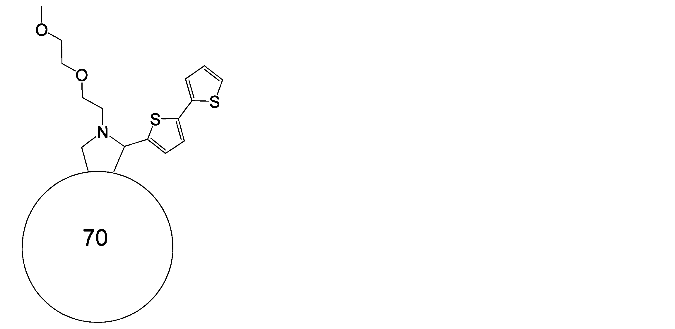
- composition 7 As a fullerene derivative represented by the formula (1), 1 part by weight of a compound represented by the following formula (a ring attached with a numerical value “70” means a C 70 fullerene skeleton) and 100 parts by weight of a solvent. Composition 7 was prepared by mixing with chlorobenzene and completely dissolving.
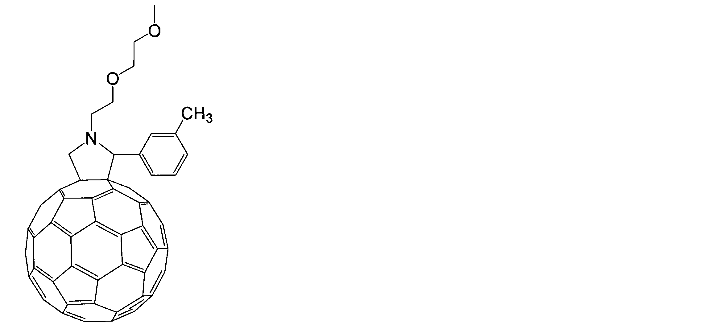
- composition 8 was prepared by mixing 1 part by weight of a compound represented by the following formula as a fullerene derivative represented by formula (1) and 100 parts by weight of chlorobenzene as a solvent and completely dissolving them.
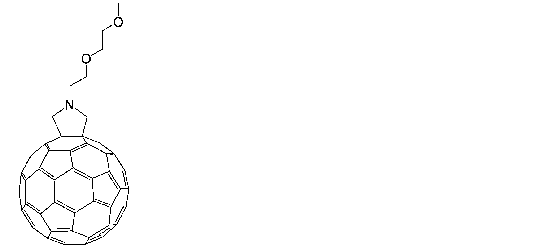
- composition 9 was prepared by mixing 1 part by weight of the compound represented by the following formula as the fullerene derivative represented by the formula (1) and 100 parts by weight of chlorobenzene as the solvent to completely dissolve the composition.
- composition 10 As a fullerene derivative represented by the formula (1), 0.5 part by weight of a compound represented by the following formula and 1.5 part by weight of [6,6] -phenyl C61-butyric acid methyl ester (C60PCBM) (frontier carbon) The composition 10 was prepared by mixing E100) and 100 parts by weight of chlorobenzene as a solvent and completely dissolving them.
- Example 1 Production and Evaluation of Photoelectric Conversion Element
- a glass substrate on which an ITO thin film that functions as an anode was formed was prepared.
- the ITO thin film was formed by the sputtering method, and its thickness was 150 nm.
- the glass substrate having the ITO thin film was subjected to ozone UV treatment to treat the surface of the ITO thin film.
- Plexcore PV2000 Hole Transport Ink included in Sigma-Aldrich's organic solar cell fabrication kit, PV2000 kit.
- Sulfonated polythiophene (thiophene-3- [2- (2-methoxyethoxy) ethoxy) -2,5-diyl) -2,5-diyl (S-P3MEET) 1.8% in 2-butoxyethanol: water (2: 3)) was applied onto the ITO film by a spin coater and heated in the atmosphere at 170 ° C. for 10 minutes to form a hole having a thickness of 50 nm. An injection layer was formed. The substrate on which the hole injection layer was formed was heated to 70 ° C. and then placed on the chuck of the spin coater, and the composition 1 heated to 70 ° C. was placed on the hole injection layer formed on the substrate at a rotational speed of 4000 rpm.
- the composition 2 was dropped on the lead iodide layer, spin-coated at 6000 rpm, and dried at 100 ° C. for 10 minutes in the air to form an active layer containing a perovskite compound having an organic-inorganic hybrid structure.
- the thickness of the active layer was about 300 nm.
- the composition 5 was applied onto the active layer using a spin coater to form an electron transport layer having a thickness of about 50 nm. Thereafter, calcium was vapor-deposited with a thickness of 4 nm by a vacuum vapor deposition machine, and then silver was vapor-deposited with a thickness of 60 nm to form a cathode. The degree of vacuum during vapor deposition was 1 ⁇ 10 ⁇ 3 to 9 ⁇ 10 ⁇ 3 Pa in all vapor deposition steps. Thereafter, in a nitrogen gas atmosphere, a sealing glass was adhered to the surface on the cathode side by UV curing using a UV curable epoxy resin, and sealed to prepare a photoelectric conversion element. The shape of the photoelectric conversion element thus obtained was a 2 mm ⁇ 2 mm square.
- the obtained photoelectric conversion element is irradiated with constant light using a solar simulator (trade name OTENTO-SUNII: AM1.5G filter, irradiance 100 mW / cm 2 , manufactured by Spectrometer Co., Ltd.), and the generated current and voltage are measured. Then, the initial photoelectric conversion efficiency (initial efficiency) was measured. Thereafter, the photoelectric conversion element was held in a weather resistance tester with a light intensity of 1 Sun and a constant temperature of 65 ° C.
- a solar simulator trade name OTENTO-SUNII: AM1.5G filter, irradiance 100 mW / cm 2 , manufactured by Spectrometer Co., Ltd.
- the photoelectric conversion element was irradiated with constant light using an illuminance of 100 mW / cm 2 ), the generated current and voltage were measured, and the photoelectric conversion efficiency (efficiency) after 20 hours was measured.
- the efficiency after 20 hours / initial efficiency was calculated as the retention rate, and is shown in Table 1 together with the composition used for forming the electron transport layer.
- Example 2 Production and Evaluation of Photoelectric Conversion Element
- a photoelectric conversion element was produced in the same manner as in Example 1 except that the composition 5 used for producing the electron transport layer was changed to the compositions 6 to 10. The initial efficiency and the efficiency after 20 hours were measured. The efficiency after 20 hours / initial efficiency was calculated as the retention rate, and is shown in Table 1 together with the composition used for forming the electron transport layer.
- the obtained photoelectric conversion element is irradiated with constant light using a solar simulator (trade name OTENTO-SUNII: AM1.5G filter, irradiance 100 mW / cm 2 , manufactured by Spectrometer Co., Ltd.), and the generated current and voltage are measured. Then, the initial photoelectric conversion efficiency (initial efficiency) was measured. Thereafter, the photoelectric conversion element was held in a weather resistance tester with a light intensity of 1 Sun and a constant temperature of 65 ° C.
- a solar simulator trade name OTENTO-SUNII: AM1.5G filter, irradiance 100 mW / cm 2 , manufactured by Spectrometer Co., Ltd.
- the photoelectric conversion element was irradiated with constant light using an illuminance of 100 mW / cm 2 ), the generated current and voltage were measured, and the photoelectric conversion efficiency after 20 hours was measured.
- the efficiency after 20 hours / initial efficiency was calculated as the retention rate, and is shown in Table 1 together with the composition used for forming the electron transport layer.
- composition 11 was prepared by dissolving 368 mg of lead iodide in 1 mL of N, N-dimethylformamide and completely dissolving by stirring at 70 ° C.
- composition 12 was prepared by completely dissolving 45 mg of methylammonium iodide in 1 mL of 2-propanol.
- composition 13 By mixing 2 parts by weight of [6,6] -phenyl C61-butyric acid methyl ester (C60PCBM) (E100 manufactured by Frontier Carbon Co.) as a fullerene derivative and 100 parts by weight of chlorobenzene as a solvent, and completely dissolving them, Composition 13 was prepared.
- composition 14 was prepared by mixing 2 parts by weight of the compound represented by the following formula as the fullerene derivative represented by the formula (1) and 100 parts by weight of chlorobenzene as a solvent and completely dissolving them.
- composition 15 was prepared by mixing 2 parts by weight of the compound represented by the following formula as the fullerene derivative represented by the formula (1) and 100 parts by weight of chlorobenzene as a solvent and completely dissolving them.
- composition 16 was prepared by mixing and completely dissolving 2 parts by weight of the compound represented by the following formula as the fullerene derivative represented by formula (1) and 100 parts by weight of chlorobenzene as the solvent.
- composition 17 0.5 weight of a polymer containing a repeating unit represented by the following formula (Poly [bis (4-phenyl) (2,4,6-trimethylphenyl) amine], average Mn 7000-10000) manufactured by Sigma-Aldrich 100 parts by weight of chlorobenzene as a solvent were mixed and completely dissolved to prepare a composition 17.
- Example 7 Production and evaluation of photoelectric conversion element A glass substrate on which an ITO thin film functioning as an anode was formed was prepared.
- the ITO thin film was formed by the sputtering method, and its thickness was 150 nm.
- the glass substrate having the ITO thin film was subjected to ozone UV treatment to treat the surface of the ITO thin film.
- the composition 17 was applied onto the ITO film by a spin coater and heated at 120 ° C. for 10 minutes in the atmosphere to form a 10 nm thick hole injection layer.
- the substrate on which the hole injection layer was formed was heated to 70 ° C., and then placed on the chuck of the spin coater.
- the composition 12 was dropped on the lead iodide layer, spin-coated at 6000 rpm, and dried at 100 ° C. for 10 minutes in the air to form an active layer containing a perovskite compound having an organic-inorganic hybrid structure.
- the thickness of the active layer was about 350 nm.
- the composition 14 was applied onto the active layer using a spin coater to form an electron transport layer having a thickness of about 50 nm. Thereafter, calcium was vapor-deposited with a thickness of 4 nm by a vacuum vapor deposition machine, and then silver was vapor-deposited with a thickness of 60 nm to form a cathode. The degree of vacuum during vapor deposition was 1 ⁇ 10 ⁇ 3 to 9 ⁇ 10 ⁇ 3 Pa in all vapor deposition steps. Thereafter, in a nitrogen gas atmosphere, a sealing glass was adhered to the surface on the cathode side by UV curing using a UV curable epoxy resin, and sealed to prepare a photoelectric conversion element. The shape of the photoelectric conversion element thus obtained was a 2 mm ⁇ 2 mm square.
- the obtained photoelectric conversion element is irradiated with constant light using a solar simulator (trade name OTENTO-SUNII: AM1.5G filter, irradiance 100 mW / cm 2 , manufactured by Spectrometer Co., Ltd.), and the generated current and voltage are measured. Then, the initial photoelectric conversion efficiency (initial efficiency) was measured. After that, the photoelectric conversion element was kept in a weather resistance tester with a light intensity of 1 Sun and a constant temperature of 65 ° C.
- a solar simulator trade name OTENTO-SUNII: AM1.5G filter, irradiance 100 mW / cm 2 , manufactured by Spectrometer Co., Ltd.
- Example 14 Production and Evaluation of Photoelectric Conversion Elements
- Example 14 except that the composition 14 used for the production of the electron transport layer was changed to the compositions 15 (Example 8) and 16 (Example 9).
- the photoelectric conversion element was produced like 7 and the initial efficiency and the photoelectric conversion efficiency after 24 hours were measured.
- the efficiency after 24 hours / initial efficiency was calculated as the retention rate, and is shown in Table 2 together with the composition used for forming the electron transport layer.
- Example 6 in which the electron transport layer includes the composition 10 containing the fullerene derivative other than the fullerene derivative represented by the formula (1) in addition to the fullerene derivative represented by the formula (1) is more The retention rate was high.
- the durability of the photoelectric conversion element against light irradiation can be further increased.
Landscapes
- Chemical & Material Sciences (AREA)
- Engineering & Computer Science (AREA)
- Materials Engineering (AREA)
- Chemical Kinetics & Catalysis (AREA)
- Electrochemistry (AREA)
- Power Engineering (AREA)
- Nanotechnology (AREA)
- Microelectronics & Electronic Packaging (AREA)
- Photovoltaic Devices (AREA)
- Nitrogen Condensed Heterocyclic Rings (AREA)
- Plural Heterocyclic Compounds (AREA)
- Indole Compounds (AREA)
Abstract
Description
[1] 陰極と、
陽極と、
前記陰極及び前記陽極の間に設けられており、ペロブスカイト化合物を含む活性層と、 前記陰極及び前記活性層の間に設けられており、下記式(1)で表されるフラーレン誘導体を含む電子輸送層と
を含む光電変換素子。
[2] 前記R1が、前記式(2)で表される基である、[1]に記載の光電変換素子。
[3〕 支持基板をさらに含み、該支持基板、前記陽極、前記活性層、前記電子輸送層及び前記陰極がこの順に設けられている、[1]又は[2]に記載の光電変換素子。
[4] 前記陽極及び前記活性層の間に設けられており、芳香族アミン化合物及び芳香族アミン残基を有する繰り返し単位を含む高分子化合物からなる群より選ばれる1種以上を含む正孔注入層をさらに含む、[1]~[3]のいずれか1つに記載の光電変換素子。
[5] [1]~[4]のいずれか1つに記載の光電変換素子を含む、太陽電池モジュール。
[6] [1]~[4]のいずれか1つに記載の光電変換素子を含む、有機光センサー。
本発明の光電変換素子の活性層の材料としては、ペロブスカイト化合物が用いられる。
本明細書において、ペロブスカイト化合物とは、ペロブスカイト構造を有する化合物をいう。ペロブスカイト化合物は、有機物及び無機物がペロブスカイト構造の構成要素となっているペロブスカイト化合物(有機無機ハイブリッド構造のペロブスカイト化合物)であることが好ましい。
式(3)中、M1は、2価の金属(例、Cu、Ni、Mn、Fe、Co、Pd、Ge、Sn、Pb、Eu)であり、3個のX1は、それぞれ独立に、F、Cl、Br又はIである。
前記式(3)で表される化合物のうち、CH3NH3PbI3、CH3NH3PbCl3、CH3NH3PbBr3、CH3NH3SnI3、CH3NH3SnCl3、CH3NH3SnBr3等がさらに好ましい。
式(4)中、R10は、炭素原子数2以上のアルキル基、アルケニル基、アラルキル基、アリール基、1価の複素環基又は1価の芳香族複素環基であり、M1は、2価の金属(例、Cu、Ni、Mn、Fe、Co、Pd、Ge、Sn、Pb、Eu)であり、4個のX1は、それぞれ独立に、F、Cl、Br又はIである。
式(5)中、M1は、2価の金属(例、Cu、Ni、Mn、Fe、Co、Pd、Ge、Sn、Pb、Eu)であり、3個のX1は、それぞれ独立に、F、Cl、Br又はIである。
本発明の光電変換素子の電子輸送層の材料としては、下記式(1)で表されるフラーレン誘導体が用いられる。

pは、2~4の整数であることが好ましく、3であることがより好ましい。上記式(3)で表される2価の基は、置換基を有していてもよい。
本発明の光電変換素子に含まれる陰極、陽極、活性層、及び電子輸送層、並びに必要に応じて含まれる他の要素(正孔注入層等)について、以下に詳しく説明する。
本発明の光電変換素子は、既に説明したとおり、一対の電極(陽極及び陰極)と、該一対の電極の間に設けられた活性層を含む。陰極及び活性層の間には、電子輸送層が設けられている。
本発明の光電変換素子は、通常、支持基板上に作製される。支持基板としては、電極を形成し、有機物の層を形成して光電変換素子を作製する際に化学的に変化しない材料により構成される基板が好適に用いられる。支持基板の材料としては、例えば、ガラス、プラスチック、高分子フィルム、シリコンが挙げられる。支持基板側から光を取り込む形態の光電変換素子の場合、支持基板には光透過性の高い基板が好適に用いられる。また不透明な支持基板上に光電変換素子を作製する場合には、支持基板を通して光を取り込むことができない。そのため、支持基板から遠い方の電極が透明又は半透明であることが好ましい。支持基板から遠い方にある電極が透明又は半透明であることにより、不透明な支持基板を用いた場合に、支持基板から遠い方にある電極を通して光を取り込むことができる。
電極は、導電性の材料で形成される。電極の材料としては、例えば、金属、金属酸化物、導電性高分子等の有機物を用いることができる。電極の材料としては、例えば、リチウム、ナトリウム、カリウム、ルビジウム、セシウム、マグネシウム、カルシウム、ストロンチウム、バリウム、アルミニウム、スカンジウム、バナジウム、亜鉛、イットリウム、インジウム、セリウム、サマリウム、ユーロピウム、テルビウム、イッテルビウム、金、銀、白金、銅、マンガン、チタン、コバルト、ニッケル、タングステン、錫等の金属、それらの金属からなる群より選ばれる2つ以上の金属を含む合金、酸化インジウム、酸化亜鉛、酸化スズ、ITO、フッ素化スズ酸化物(FTO)、インジウム亜鉛酸化物(IZO)、グラファイト、グラファイト層間化合物等が挙げられる。合金の例としては、マグネシウム-銀合金、マグネシウム-インジウム合金、マグネシウム-アルミニウム合金、インジウム-銀合金、リチウム-アルミニウム合金、リチウム-マグネシウム合金、リチウム-インジウム合金、カルシウム-アルミニウム合金等が挙げられる。導電性高分子の例としては、ポリアニリン及びその誘導体、ポリチオフェン及びその誘導体が挙げられる。
電極は、単層の形態であっても、複数の層が積層された形態であってもよい。
電極の形成方法に特に制限はなく、例えば、前記電極の材料を真空蒸着法、スパッタリング法、イオンプレーティング法、メッキ法、塗布法等によって電極を形成すべき層上又は支持基板上に形成することができる。電極の材料が、ポリアニリン及びその誘導体、ポリチオフェン及びその誘導体、ナノ粒子、ナノワイヤ又はナノチューブを含むエマルション(乳濁液)又はサスペンション(懸濁液)等である場合、好ましくは塗布法によって電極を形成することができる。また、電極の材料が導電性物質を含む場合、導電性物質を含む塗布液、金属インキ、金属ペースト、溶融状態の低融点金属等を用いて、塗布法によって電極を形成してもよい。塗布液等を塗布するための方法としては、例えば、スピンコート法、キャスティング法、マイクログラビアコート法、グラビアコート法、バーコート法、ロールコート法、ワイヤーバーコート法、ディップコート法、スプレーコート法、スクリーン印刷法、フレキソ印刷法、オフセット印刷法、インクジェット印刷法、ディスペンサー印刷法、ノズルコート法、キャピラリーコート法を挙げることができ、これらの中でもスピンコート法、フレキソ印刷法、インクジェット印刷法、ディスペンサー印刷法が好ましい。
活性層は、光エネルギーを電気エネルギーに変換する機能を有する層である。
本発明の光電変換素子の活性層は、ペロブスカイト化合物を含む。ペロブスカイト化合物の具体例及び好ましい例は、上述のとおりである。
ペロブスカイト化合物を含む活性層を形成する方法は特に制限されない。活性層の形成方法としては、例えば、塗布法が挙げられる。活性層の形成工程をより簡便にする観点からはペロブスカイト化合物を含む活性層を塗布法によって形成することが好ましい。塗布法に用いられ得る塗布液は、前記ペロブスカイト化合物を含む溶液であっても、層の形成後にペロブスカイト化合物に自己組織化反応により変換し得る前駆体を含む溶液であってもよい。このような前駆体としては、例えば、CH3NH3PbI3、CH3NH3PbBr3、(CH3(CH2)nCHCH3NH3)2PbI4(ここでnは5~8の整数である。)、(C6H5C2H4NH3)2PbBr4が挙げられる。
また前記活性層を形成するための塗布液は、2種類以上の溶媒を含んでいてもよく、上記で例示した溶媒を2種類以上含んでいてもよい。
本発明の光電変換素子では、陰極と活性層との間に、電子輸送層が設けられる。電子輸送層は、上記式(1)で表されるフラーレン誘導体を含む。式(1)で表されるフラーレン誘導体の具体例及び好ましい例は、既に説明したとおりである。

電子輸送層の形成方法に特に制限はない。電子輸送層の形成方法としては、例えば、真空蒸着法、塗布法が挙げられる。電子輸送層は、塗布法により形成することが好ましい。
電子輸送層を塗布法により形成する際に用いられる塗布液は、式(1)で表されるフラーレン誘導体に加えて、必要に応じて他の電子輸送性材料を含み得る。電子輸送層は、式(1)で表されるフラーレン誘導体と必要に応じて添加される他の電子輸送性材料と溶媒とを含む塗布液を、活性層に塗布することにより形成することが好ましい。塗布液は、塗布液が塗布される層(活性層など)に損傷を与えないか又は与え難い塗布液を用いることが好ましく、具体的には塗布液が塗布される層(活性層など)を溶解しないか又は溶解し難い塗布液とすることが好ましい。
本発明の光電変換素子は、上述の活性層及び電子輸送層の他に、種々の機能を発揮するその他の任意の層を含んでいてもよい。その他の任意の層としては、例えば、正孔注入層及び正孔輸送層が挙げられる。
本発明の光電変換素子は、陽極及び活性層の間に設けられており、芳香族アミン化合物及び芳香族アミン残基を有する繰り返し単位を含む高分子化合物からなる群より選ばれる1種以上を含む正孔注入層をさらに含んでいてもよい。

ここで複素環式化合物とは、環式構造をもつ有機化合物のうち、環を構成する元素が炭素原子だけでなく、酸素原子、硫黄原子、窒素原子、リン原子、ホウ素原子、ヒ素原子などのヘテロ原子を環内に含む化合物をいう。2価の複素環基(B1)が有し得る置換基の例としては、アルキル基、アルコキシ基、アルキルチオ基、アリール基、アリールオキシ基、アリールチオ基、アリールアルキル基、アリールアルコキシ基、アリールアルキルチオ基、アリールアルケニル基、アリールアルキニル基、アミノ基、置換アミノ基、シリル基、置換シリル基、シリルオキシ基、置換シリルオキシ基、ハロゲン原子、アシル基、アシルオキシ基、イミノ基、アミド基、イミド基、1価の複素環基、カルボキシル基、置換カルボキシル基、シアノ基等が挙げられ、アルキル基、アルコキシ基、アルキルチオ基、アリール基、アリールオキシ基、アリールチオ基、置換アミノ基、置換シリル基、置換シリルオキシ基、1価の複素環基が好ましい。置換基を有しない2価の複素環基の炭素原子数は通常3~60程度である。
ここで複素環式化合物とは、環式構造をもつ有機化合物のうち、環を構成する元素が炭素原子だけでなく、酸素原子、硫黄原子、窒素原子、リン原子、ホウ素原子、ヒ素原子などのヘテロ原子を環内に含む化合物をいう。2価の複素環基(B1)が有し得る置換基の例としては、アルキル基、アルコキシ基、アルキルチオ基、アリール基、アリールオキシ基、アリールチオ基、アリールアルキル基、アリールアルコキシ基、アリールアルキルチオ基、アリールアルケニル基、アリールアルキニル基、アミノ基、置換アミノ基、シリル基、置換シリル基、シリルオキシ基、置換シリルオキシ基、ハロゲン原子、アシル基、アシルオキシ基、イミノ基、アミド基、イミド基、1価の複素環基、カルボキシル基、置換カルボキシル基、シアノ基等が挙げられ、アルキル基、アルコキシ基、アルキルチオ基、アリール基、アリールオキシ基、アリールチオ基、置換アミノ基、置換シリル基、置換シリルオキシ基、1価の複素環基が好ましい。置換基を有しない2価の複素環基の炭素原子数は通常3~60程度である。

―Ar12-X1―(Ar13-X2)c―Ar14- (7)
-Ar12-X2- (8)
-X2- (9)
X2は-CR2=CR3-で表される基、-C≡C-で表される基、-N(R4)-で表される基、又は-(SiR5R6)d-で表される基を表す。R2及びR3は、それぞれ独立に水素原子、アルキル基、アリール基、1価の複素環基、カルボキシル基、置換カルボキシル基又はシアノ基を表す。R4、R5及びR6は、それぞれ独立に水素原子、アルキル基、アリール基、1価の複素環基又はアリールアルキル基を表す。cは0~2の整数を表す。dは1~12の整数を表す。Ar13、R2、R3、R5及びR6がそれぞれ複数存在する場合、それらは同一であっても異なっていてもよい。


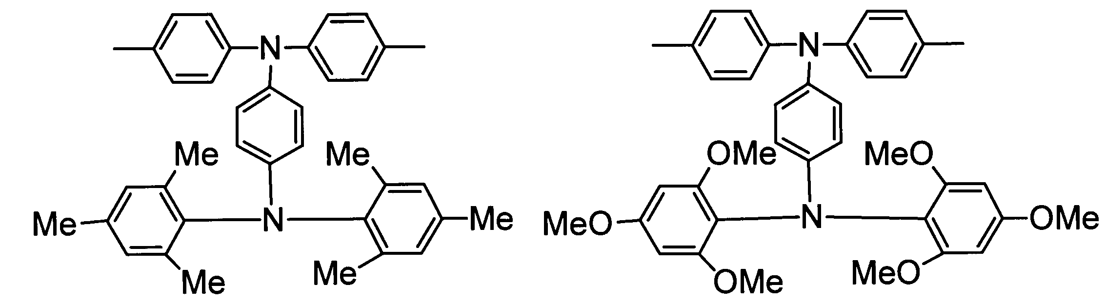

正孔注入層の形成方法は特に限定されない。正孔注入層は例えば前述した正孔注入層の構成材料と溶媒とを含む塗布液を、正孔注入層が形成されるべき層に塗布することにより形成することができる。
正孔輸送層は、正孔注入層と活性層との間に設けられ、正孔を輸送し、かつ電子をブロックする機能を有する。正孔輸送層を設けることで、より高効率な光電変換素子とすることができる。正孔輸送層としては、アミン残基を含む低分子化合物、アミン残基を有する繰り返し単位を含む高分子化合物などが挙げられる。正孔注入層に、芳香族アミン残基を有する低分子化合物、芳香族アミン残基を有する繰り返し単位を含む高分子化合物を用いる場合には、特にこのような正孔輸送層を設けなくてもよい。

正孔輸送層は、既に説明した正孔注入層、活性層と同様にして形成することができる。
正孔輸送層の構成材料と溶媒とを含む塗布液を塗布する形成方法の具体例及び好ましい例としては、活性層を形成する方法において既に説明した方法が挙げられる。
ヨウ化鉛460mgを1mLのN,N-ジメチルホルムアミドに溶解させ、70℃で攪拌することで完溶させることにより、組成物1を調製した。
ヨウ化メチルアンモニウム45mgを1mLの2-プロパノールに完溶させることにより、組成物2を調製した。
フラーレンの誘導体として1重量部の[6,6]-フェニルC61-酪酸メチルエステル(C60PCBM)(フロンティアカーボン社製 E100)と、溶媒として100重量部のクロロベンゼンとを混合して完溶させることにより、組成物3を調製した。
フラーレンの誘導体として1重量部の[6,6]-フェニルC71-酪酸メチルエステル(C70PCBM)(アメリカンダイソース社製 ADS71BFA)と、溶媒として100重量部のクロロベンゼンとを混合して完溶させることにより、組成物4を調製した。
式(1)で表されるフラーレン誘導体として1重量部の下記式で表される化合物と、溶媒として100重量部のクロロベンゼンとを混合して完溶させることにより、組成物5を調製した。

前記式(1)で表されるフラーレン誘導体として1重量部の下記式で表される化合物と、溶媒として100重量部のクロロベンゼンとを混合して完溶させることにより、組成物6を調製した。

式(1)で表されるフラーレン誘導体として1重量部の下記式で表される化合物(数値「70」が付された環はC70フラーレン骨格を意味する。)と、溶媒として100重量部のクロロベンゼンとを混合して完溶させることにより、組成物7を調製した。
式(1)で表されるフラーレン誘導体として1重量部の下記式で表される化合物と、溶媒として100重量部のクロロベンゼンとを混合して完溶させることにより、組成物8を調製した。
式(1)で表されるフラーレン誘導体として1重量部の下記式で表される化合物と、溶媒として100重量部のクロロベンゼンとを混合して完溶させることにより、組成物9を調製した。

式(1)で表されるフラーレン誘導体として0.5重量部の下記式で表される化合物と、1.5重量部の[6,6]-フェニルC61-酪酸メチルエステル(C60PCBM)(フロンティアカーボン社製 E100)と、溶媒として100重量部のクロロベンゼンとを混合して完溶させることにより、組成物10を調製した。
陽極として機能するITO薄膜が形成されたガラス基板を用意した。ITO薄膜はスパッタリング法によって形成され、その厚さは150nmであった。前記ITO薄膜を有するガラス基板をオゾンUV処理し、ITO薄膜の表面処理を行った。次に、Plexcore PV2000 Hole Transport Ink(シグマ・アルドリッチ社の有機太陽電池作製キット、PV2000 kitに含まれる。Sulfonated polythiophene(thiophene-3-[2-(2-methoxyethoxy)ethoxy]-2,5-diyl) (S-P3MEET) 1.8% in 2-butoxyethanol:water (2:3))をスピンコーターによりITO膜上に塗布し、大気中170℃で10分間加熱することにより、厚さ50nmの正孔注入層を形成した。正孔注入層を形成した基板を70℃に加熱した後、スピンコーターのチャック上に載せ、基板に形成された正孔注入層上に、70℃に加熱した組成物1を4000rpmの回転数でスピンコーターを用いて塗布し、窒素ガス雰囲気下で風乾させ、ヨウ化鉛層を得た。その後、ヨウ化鉛層上に前記組成物2を滴下し、6000rpmでスピンコートし、大気中100℃で10分間乾燥させることで、有機無機ハイブリッド構造のペロブスカイト化合物を含む活性層を形成した。活性層の厚さは約300nmであった。
電子輸送層の作成に使用した組成物5を、組成物6~10に変更した以外は、実施例1と同様にして光電変換素子を作成し、初期効率と20時間後の効率とを測定した。20時間後の効率/初期効率を保持率として算出し、電子輸送層の形成に使用された組成物と併せて表1に示した。
電子輸送層の作成に使用した組成物5を、組成物3(比較例1)又は4(比較例2)に変更した以外は、実施例1と同様にして光電変換素子を作製し、初期効率と20時間後の効率とを測定した。20時間後の効率/初期効率を保持率として算出し、電子輸送層の作成に使用された組成物と併せて表1に示した。
ヨウ化鉛368mgを1mLのN,N-ジメチルホルムアミドに溶解させ、70℃で攪拌することで完溶させることにより、組成物11を調製した。
ヨウ化メチルアンモニウム45mgを1mLの2-プロパノールに完溶させることにより、組成物12を調製した。
フラーレンの誘導体として2重量部の[6,6]-フェニルC61-酪酸メチルエステル(C60PCBM)(フロンティアカーボン社製 E100)と、溶媒として100重量部のクロロベンゼンとを混合して完溶させることにより、組成物13を調製した。
式(1)で表されるフラーレン誘導体として2重量部の下記式で表される化合物と、溶媒として100重量部のクロロベンゼンとを混合して完溶させることにより、組成物14を調製した。
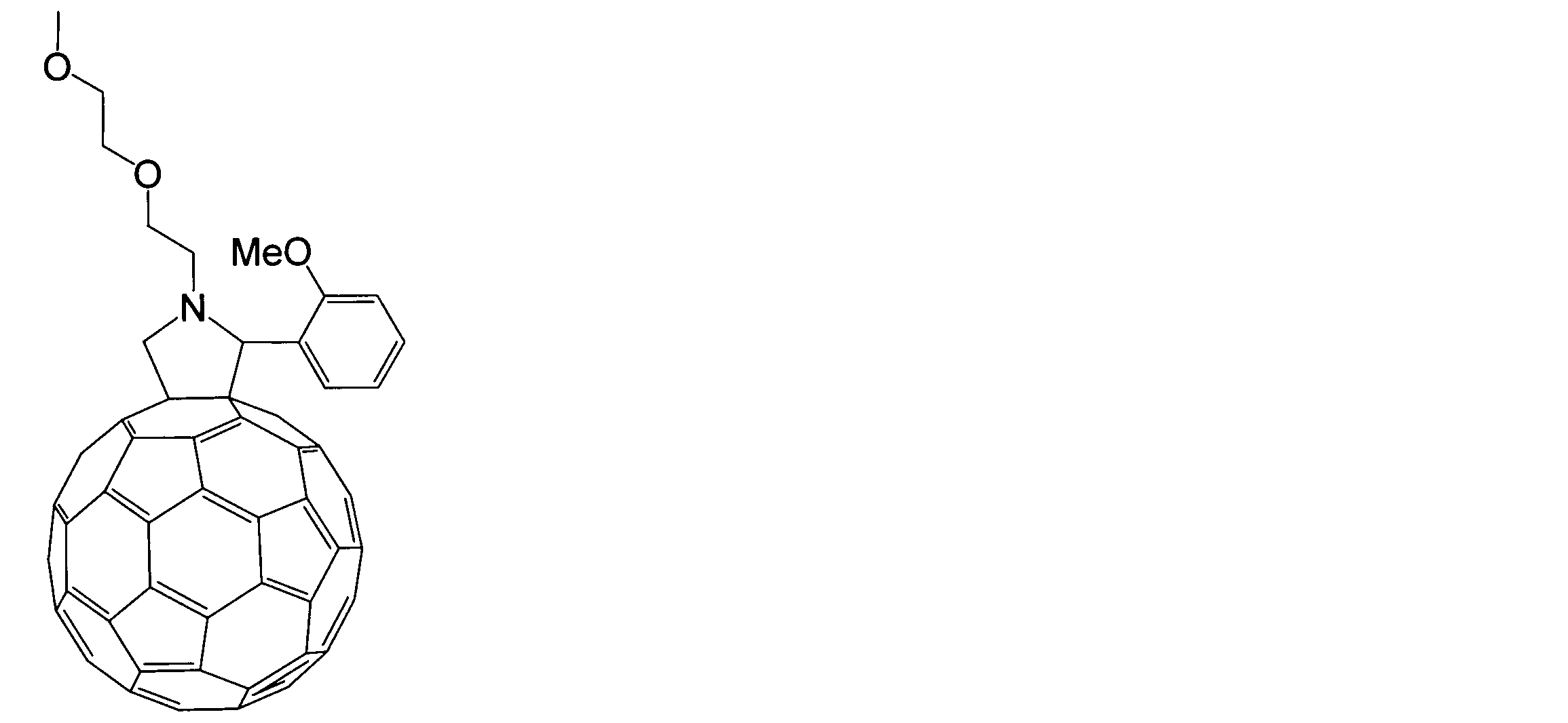
前記式(1)で表されるフラーレン誘導体として2重量部の下記式で表される化合物と、溶媒として100重量部のクロロベンゼンとを混合して完溶させることにより、組成物15を調製した。

式(1)で表されるフラーレン誘導体として2重量部の下記式で表される化合物と、溶媒として100重量部のクロロベンゼンとを混合して完溶させることにより、組成物16を調製した。
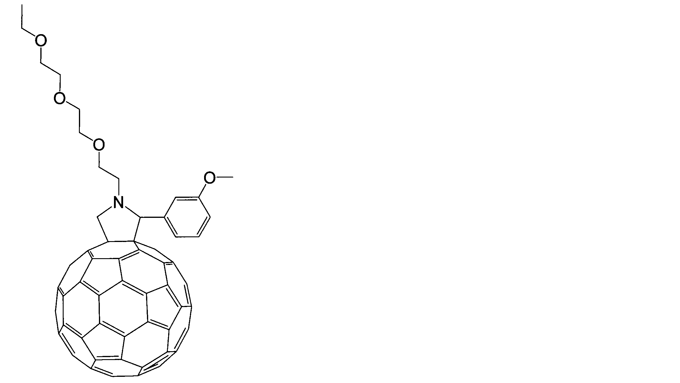
下記式で表される繰り返し単位を含む高分子化合物(シグマ・アルドリッチ社製 Poly[bis(4-phenyl)(2,4,6-trimethylphenyl)amine]、average Mn 7000-10000)を0.5重量部、溶媒として100重量部のクロロベンゼンを混合して完溶させて、組成物17を調製した。

陽極として機能するITO薄膜が形成されたガラス基板を用意した。ITO薄膜はスパッタリング法によって形成され、その厚さは150nmであった。前記ITO薄膜を有するガラス基板をオゾンUV処理し、ITO薄膜の表面処理を行った。次に、組成物17をスピンコーターによりITO膜上に塗布し、大気中120℃で10分間加熱することにより、厚さ10nmの正孔注入層を形成した。正孔注入層を形成した基板を70℃に加熱した後、スピンコーターのチャック上に載せ、基板に形成された正孔注入層上に、70℃に加熱した組成物11を2000rpmの回転数でスピンコーターを用いて塗布し、窒素ガス雰囲気下で風乾させ、ヨウ化鉛層を得た。その後、ヨウ化鉛層上に前記組成物12を滴下し、6000rpmでスピンコートし、大気中100℃で10分間乾燥させることで、有機無機ハイブリッド構造のペロブスカイト化合物を含む活性層を形成した。活性層の厚さは約350nmであった。
電子輸送層の作成に使用した組成物14を、組成物15(実施例8)、16(実施例9)に変更した以外は、実施例7と同様にして光電変換素子を作製し、初期効率と24時間後の光電変換効率とを測定した。24時間後の効率/初期効率を保持率として算出し、電子輸送層の形成に使用された組成物と併せて表2に示した。
電子輸送層の作成に使用した組成物14を、組成物13に変更した以外は、実施例7と同様にして光電変換素子を作製し、初期効率と24時間後の効率とを測定した。24時間後の効率/初期効率を保持率として算出し、電子輸送層の作成に使用された組成物と併せて表2に示した。


Claims (6)
- 陰極と、
陽極と、
前記陰極及び前記陽極の間に設けられており、ペロブスカイト化合物を含む活性層と、
前記陰極及び前記活性層の間に設けられており、下記式(1)で表されるフラーレン誘導体を含む電子輸送層と
を含む光電変換素子。


- 前記R1が、前記式(2)で表される基である、請求項1に記載の光電変換素子。
- 支持基板をさらに含み、該支持基板、前記陽極、前記活性層、前記電子輸送層及び前記陰極がこの順に設けられている、請求項1又は2に記載の光電変換素子。
- 前記陽極及び前記活性層の間に設けられており、芳香族アミン化合物及び芳香族アミン残基を有する繰り返し単位を含む高分子化合物からなる群より選ばれる1種以上を含む正孔注入層をさらに含む、請求項1~3のいずれか1項に記載の光電変換素子。
- 請求項1~4のいずれか1項に記載の光電変換素子を含む、太陽電池モジュール。
- 請求項1~4のいずれか1項に記載の光電変換素子を含む、有機光センサー。
Priority Applications (4)
| Application Number | Priority Date | Filing Date | Title |
|---|---|---|---|
| DE112016001525.9T DE112016001525T5 (de) | 2015-03-30 | 2016-03-24 | Photoelektrische Wandlervorrichtung |
| CN201680020166.7A CN107431135A (zh) | 2015-03-30 | 2016-03-24 | 光电转换元件 |
| JP2017509880A JP6674948B2 (ja) | 2015-03-30 | 2016-03-24 | 光電変換素子 |
| US15/559,233 US20180075978A1 (en) | 2015-03-30 | 2016-03-24 | Photoelectric conversion device |
Applications Claiming Priority (4)
| Application Number | Priority Date | Filing Date | Title |
|---|---|---|---|
| JP2015-069735 | 2015-03-30 | ||
| JP2015069735 | 2015-03-30 | ||
| JP2015168234 | 2015-08-27 | ||
| JP2015-168234 | 2015-08-27 |
Publications (1)
| Publication Number | Publication Date |
|---|---|
| WO2016158698A1 true WO2016158698A1 (ja) | 2016-10-06 |
Family
ID=57004269
Family Applications (1)
| Application Number | Title | Priority Date | Filing Date |
|---|---|---|---|
| PCT/JP2016/059484 Ceased WO2016158698A1 (ja) | 2015-03-30 | 2016-03-24 | 光電変換素子 |
Country Status (5)
| Country | Link |
|---|---|
| US (1) | US20180075978A1 (ja) |
| JP (1) | JP6674948B2 (ja) |
| CN (1) | CN107431135A (ja) |
| DE (1) | DE112016001525T5 (ja) |
| WO (1) | WO2016158698A1 (ja) |
Cited By (4)
| Publication number | Priority date | Publication date | Assignee | Title |
|---|---|---|---|---|
| WO2018079323A1 (ja) * | 2016-10-24 | 2018-05-03 | 住友化学株式会社 | 光電変換素子 |
| JP2018195768A (ja) * | 2017-05-19 | 2018-12-06 | 富士フイルム株式会社 | 光電変換素子、太陽電池、光電変換素子の製造方法及び光電変換素子用組成物 |
| JP2019175919A (ja) * | 2018-03-27 | 2019-10-10 | 三菱ケミカル株式会社 | 光電変換素子及び太陽電池モジュール |
| JP2019212763A (ja) * | 2018-06-05 | 2019-12-12 | 住友化学株式会社 | 光電変換素子 |
Families Citing this family (2)
| Publication number | Priority date | Publication date | Assignee | Title |
|---|---|---|---|---|
| EP3770976A4 (en) * | 2018-03-23 | 2021-12-22 | Sumitomo Chemical Company, Limited | ELEMENT FOR PHOTOELECTRIC CONVERSION |
| CN110400876A (zh) * | 2018-04-25 | 2019-11-01 | 杭州纤纳光电科技有限公司 | 一种掺杂抗氧化剂的钙钛矿薄膜及其制备方法和应用 |
Citations (4)
| Publication number | Priority date | Publication date | Assignee | Title |
|---|---|---|---|---|
| WO2009035024A1 (ja) * | 2007-09-12 | 2009-03-19 | Sumitomo Chemical Company, Limited | フラーレン誘導体 |
| US20130160827A1 (en) * | 2011-12-05 | 2013-06-27 | University Of Washington Through Its Center For Commercialization | Fullerene surfactants and their use in polymer solar cells |
| WO2014045021A1 (en) * | 2012-09-18 | 2014-03-27 | Isis Innovation Limited | Optoelectronic device |
| EP2846371A1 (en) * | 2013-09-10 | 2015-03-11 | Ecole Polytechnique Fédérale de Lausanne (EPFL) | Inverted solar cell and process for producing the same |
Family Cites Families (7)
| Publication number | Priority date | Publication date | Assignee | Title |
|---|---|---|---|---|
| JP5323393B2 (ja) * | 2007-09-12 | 2013-10-23 | 住友化学株式会社 | フラーレン誘導体 |
| JP5229150B2 (ja) * | 2009-07-31 | 2013-07-03 | 住友化学株式会社 | フラーレン誘導体 |
| JP5639753B2 (ja) * | 2009-10-30 | 2014-12-10 | 住友化学株式会社 | フラーレン誘導体 |
| US9267003B2 (en) * | 2012-01-30 | 2016-02-23 | Sumitomo Chemical Company, Limited | Polymer compound, composition, and light-emitting device using the same |
| CN103664740A (zh) * | 2012-09-05 | 2014-03-26 | 北京师范大学 | 一种新型的醇溶性富勒烯衍生物的制备 |
| TWI485154B (zh) * | 2013-05-09 | 2015-05-21 | Univ Nat Cheng Kung | 具鈣鈦礦結構吸光材料之有機混成太陽能電池及其製造方法 |
| CN104051629B (zh) * | 2014-06-28 | 2017-10-20 | 福州大学 | 一种基于喷涂工艺制备钙钛矿型太阳能电池的方法 |
-
2016
- 2016-03-24 CN CN201680020166.7A patent/CN107431135A/zh active Pending
- 2016-03-24 JP JP2017509880A patent/JP6674948B2/ja active Active
- 2016-03-24 WO PCT/JP2016/059484 patent/WO2016158698A1/ja not_active Ceased
- 2016-03-24 US US15/559,233 patent/US20180075978A1/en not_active Abandoned
- 2016-03-24 DE DE112016001525.9T patent/DE112016001525T5/de not_active Withdrawn
Patent Citations (4)
| Publication number | Priority date | Publication date | Assignee | Title |
|---|---|---|---|---|
| WO2009035024A1 (ja) * | 2007-09-12 | 2009-03-19 | Sumitomo Chemical Company, Limited | フラーレン誘導体 |
| US20130160827A1 (en) * | 2011-12-05 | 2013-06-27 | University Of Washington Through Its Center For Commercialization | Fullerene surfactants and their use in polymer solar cells |
| WO2014045021A1 (en) * | 2012-09-18 | 2014-03-27 | Isis Innovation Limited | Optoelectronic device |
| EP2846371A1 (en) * | 2013-09-10 | 2015-03-11 | Ecole Polytechnique Fédérale de Lausanne (EPFL) | Inverted solar cell and process for producing the same |
Non-Patent Citations (1)
| Title |
|---|
| C.H.CHIANG: "Planar heterojunction perovskite/ PC71BM solar cells with enhanced open-circuit voltage via a (2/1)-step spin-coating process", JOURNAL OF MATERIALS CHEMISTRY A, vol. 2, no. 38, 2014, pages 15897 - 15903, XP055319922 * |
Cited By (6)
| Publication number | Priority date | Publication date | Assignee | Title |
|---|---|---|---|---|
| WO2018079323A1 (ja) * | 2016-10-24 | 2018-05-03 | 住友化学株式会社 | 光電変換素子 |
| JPWO2018079323A1 (ja) * | 2016-10-24 | 2019-09-12 | 住友化学株式会社 | 光電変換素子 |
| JP2018195768A (ja) * | 2017-05-19 | 2018-12-06 | 富士フイルム株式会社 | 光電変換素子、太陽電池、光電変換素子の製造方法及び光電変換素子用組成物 |
| JP2019175919A (ja) * | 2018-03-27 | 2019-10-10 | 三菱ケミカル株式会社 | 光電変換素子及び太陽電池モジュール |
| JP7482362B2 (ja) | 2018-03-27 | 2024-05-14 | 三菱ケミカル株式会社 | 光電変換素子及び太陽電池モジュール |
| JP2019212763A (ja) * | 2018-06-05 | 2019-12-12 | 住友化学株式会社 | 光電変換素子 |
Also Published As
| Publication number | Publication date |
|---|---|
| JP6674948B2 (ja) | 2020-04-01 |
| US20180075978A1 (en) | 2018-03-15 |
| DE112016001525T5 (de) | 2018-01-04 |
| CN107431135A (zh) | 2017-12-01 |
| JPWO2016158698A1 (ja) | 2018-03-08 |
Similar Documents
| Publication | Publication Date | Title |
|---|---|---|
| JP6697886B2 (ja) | 光電変換素子 | |
| JP6674948B2 (ja) | 光電変換素子 | |
| JP5682108B2 (ja) | フラーレン誘導体 | |
| WO2011052568A1 (ja) | 有機光電変換素子 | |
| WO2018079323A1 (ja) | 光電変換素子 | |
| JP6798499B2 (ja) | ペロブスカイト光電変換素子 | |
| WO2010137634A1 (ja) | 有機光電変換素子 | |
| JP6687025B2 (ja) | 光電変換素子 | |
| JP5639783B2 (ja) | 光電変換素子 | |
| JP6718249B2 (ja) | 光電変換素子の製造方法及び光電変換素子 | |
| JP5715796B2 (ja) | 有機光電変換素子の製造方法 | |
| JP6697816B2 (ja) | 光電変換素子 | |
| JP2019212763A (ja) | 光電変換素子 | |
| CN107210371A (zh) | 光电转换元件及其制造方法 | |
| JP6995596B2 (ja) | 光電変換素子 | |
| JP2015099810A (ja) | 有機光電変換素子の製造方法 | |
| JP6032284B2 (ja) | 有機光電変換素子の製造方法 | |
| JP2011246594A (ja) | 高分子化合物及びそれを用いた光電変換素子 | |
| JP6697820B2 (ja) | 光電変換素子及びフラーレン誘導体 | |
| JP2017103268A (ja) | 光電変換素子 | |
| JP2019024068A (ja) | 光電変換素子 | |
| WO2011052578A1 (ja) | 有機光電変換素子の製造方法 | |
| JP2014197688A (ja) | 光電変換素子 |
Legal Events
| Date | Code | Title | Description |
|---|---|---|---|
| 121 | Ep: the epo has been informed by wipo that ep was designated in this application |
Ref document number: 16772579 Country of ref document: EP Kind code of ref document: A1 |
|
| ENP | Entry into the national phase |
Ref document number: 2017509880 Country of ref document: JP Kind code of ref document: A |
|
| WWE | Wipo information: entry into national phase |
Ref document number: 15559233 Country of ref document: US |
|
| WWE | Wipo information: entry into national phase |
Ref document number: 112016001525 Country of ref document: DE |
|
| 122 | Ep: pct application non-entry in european phase |
Ref document number: 16772579 Country of ref document: EP Kind code of ref document: A1 |