WO2016127618A1 - 阵列基板制造方法、阵列基板和显示装置 - Google Patents
阵列基板制造方法、阵列基板和显示装置 Download PDFInfo
- Publication number
- WO2016127618A1 WO2016127618A1 PCT/CN2015/087337 CN2015087337W WO2016127618A1 WO 2016127618 A1 WO2016127618 A1 WO 2016127618A1 CN 2015087337 W CN2015087337 W CN 2015087337W WO 2016127618 A1 WO2016127618 A1 WO 2016127618A1
- Authority
- WO
- WIPO (PCT)
- Prior art keywords
- film layer
- insulating film
- substrate
- metal pattern
- pattern
- Prior art date
- Legal status (The legal status is an assumption and is not a legal conclusion. Google has not performed a legal analysis and makes no representation as to the accuracy of the status listed.)
- Ceased
Links
Images




Classifications
-
- H—ELECTRICITY
- H10—SEMICONDUCTOR DEVICES; ELECTRIC SOLID-STATE DEVICES NOT OTHERWISE PROVIDED FOR
- H10D—INORGANIC ELECTRIC SEMICONDUCTOR DEVICES
- H10D30/00—Field-effect transistors [FET]
- H10D30/60—Insulated-gate field-effect transistors [IGFET]
- H10D30/67—Thin-film transistors [TFT]
- H10D30/6729—Thin-film transistors [TFT] characterised by the electrodes
- H10D30/673—Thin-film transistors [TFT] characterised by the electrodes characterised by the shapes, relative sizes or dispositions of the gate electrodes
-
- H—ELECTRICITY
- H10—SEMICONDUCTOR DEVICES; ELECTRIC SOLID-STATE DEVICES NOT OTHERWISE PROVIDED FOR
- H10D—INORGANIC ELECTRIC SEMICONDUCTOR DEVICES
- H10D30/00—Field-effect transistors [FET]
- H10D30/60—Insulated-gate field-effect transistors [IGFET]
- H10D30/67—Thin-film transistors [TFT]
- H10D30/6704—Thin-film transistors [TFT] having supplementary regions or layers in the thin films or in the insulated bulk substrates for controlling properties of the device
- H10D30/6725—Thin-film transistors [TFT] having supplementary regions or layers in the thin films or in the insulated bulk substrates for controlling properties of the device having supplementary regions or layers for improving the flatness of the device
-
- H—ELECTRICITY
- H10—SEMICONDUCTOR DEVICES; ELECTRIC SOLID-STATE DEVICES NOT OTHERWISE PROVIDED FOR
- H10D—INORGANIC ELECTRIC SEMICONDUCTOR DEVICES
- H10D30/00—Field-effect transistors [FET]
- H10D30/60—Insulated-gate field-effect transistors [IGFET]
- H10D30/67—Thin-film transistors [TFT]
- H10D30/6758—Thin-film transistors [TFT] characterised by the insulating substrates
Definitions
- the present invention relates to the field of display technologies, and in particular, to an array substrate manufacturing method, an array substrate, and a display device.
- the array substrate is an important component of the display device, and generally includes a substrate and a gate line on the substrate, a common electrode trace, an insulating film layer, a semiconductor layer, and a source/drain metal layer (source drain and data line).
- a metal pattern such as a pattern of gate lines, is first formed on the substrate, and then an insulating film layer is coated on the substrate on which the metal pattern is formed, and then a semiconductor layer is formed on the substrate on which the insulating film layer is applied. And a source and drain metal layer pattern.
- the insulating film layer has an overlapping region of the insulating film layer and the metal pattern (the overlapping region refers to a projection region of the metal pattern on the insulating film layer), and an overlapping region of the insulating film layer and the metal pattern on the insulating film layer Also referred to as an overlapping region of the insulating film layer, the overlapping regions of the insulating film layer are all formed with bumps, and other patterns (source drains, data lines) which are then formed on the insulating film layer also have corresponding bumps ( The bump of the source drain, the bump of the data line).
- the other patterns (such as the pattern of the source and drain electrodes) formed on the overlapping regions of the insulating film layer are highly convex, and thus the disconnection is likely to occur, which affects the yield of the product.
- An array substrate manufacturing method, an array substrate, and a display device are provided.
- a method of fabricating an array substrate includes the steps of:
- a semiconductor layer and a source/drain metal layer pattern are formed on the substrate on which the insulating film layer is formed.
- the step of forming a metal pattern having a thickness d on the substrate comprises the steps of:
- a metal pattern having a thickness d is formed in the trench.
- the step of forming an insulating film layer on the substrate on which the metal pattern is formed comprises the steps of:
- the step of thinning the overlapping region comprises the steps of:
- the overlapping region of the initial insulating film layer is processed by one patterning process to make the difference in height difference between the overlapped region of the processed initial insulating film layer and other regions of the processed initial insulating film layer after treatment
- the value is less than the thickness d.
- the step of forming an insulating film layer on the substrate on which the metal pattern is formed comprises the steps of:
- the step of thinning the overlapping region of the organic film layer comprises the steps of:
- the step of forming an insulating film layer on the substrate on which the metal pattern is formed comprises the steps of:
- the insulating material is an organic material.
- the step of forming the insulating film layer on the substrate on which the reverse pattern is formed may include the steps of: forming an initial insulating film layer on the substrate on which the reverse pattern is formed, wherein the initial insulating layer An overlapping region of the film layer and the metal pattern is convex on the initial insulating film layer; and an overlapping region of the initial insulating film layer is thinned to obtain the insulating film layer such that the insulating layer The absolute value of the height difference between the overlapping region of the film layer and the other regions of the insulating film layer is smaller than the thickness d.
- the step of performing the thinning treatment on the overlapping region may include the step of processing the overlapping region of the initial insulating film layer by one patterning process to make the processed initial insulating film layer
- the absolute value of the height difference between the overlap region and the other regions of the treated initial insulating film layer is smaller than the thickness d.
- the step of forming an insulating film layer on the substrate on which the reverse pattern is formed may include the steps of: forming an organic film layer on the substrate on which the reverse pattern is formed, wherein the organic film layer The metal pattern has an overlapping region, and an overlapping region of the organic film layer is convex on the organic film layer; and an overlapping region of the organic film layer is thinned to make the organic after processing An absolute value of a height difference between an overlapping region of the film layer and other regions of the organic film layer after the treatment is smaller than the thickness d; and the insulating film layer is formed on the substrate on which the organic film layer is formed; or Forming an insulating organic film layer on the substrate on which the reverse pattern is formed, wherein the organic film layer and the metal pattern have overlapping regions, and an overlapping region of the organic film layer is convex on the organic film layer And performing an thinning treatment on the overlapping region of the organic film layer such that the absolute value of the height difference between the overlapped region of the treated organic film layer and the other
- the step of thinning the overlapping region of the organic film layer may include the steps of: exposing and developing an overlapping region of the organic film layer to make the treated organic film layer intersect The absolute value of the height difference between the stacked region and the other regions of the treated organic film layer is smaller than the thickness d.
- the metal pattern is a pattern including gate lines or a pattern including gate lines and common electrode traces.
- a difference in height between an overlapping region of the insulating film layer and other regions of the insulating film layer is zero.
- an array substrate comprising:
- the absolute value of the height difference is less than the thickness d;
- a semiconductor layer and a source/drain metal layer pattern formed on the insulating film layer are semiconductor layers and a source/drain metal layer pattern formed on the insulating film layer.
- the array substrate further includes: a trench formed on the substrate; wherein the metal pattern having a thickness d is formed in the trench.
- the array substrate further includes: an organic film layer formed between the insulating film layer and the metal pattern, wherein the organic film layer and the metal pattern have overlapping regions.
- the insulating film layer is an organic insulating film layer.
- the array substrate further includes: a reverse pattern of a region on the substrate below the insulating film layer where the metal pattern is not formed, wherein the reverse pattern is formed of an insulating material.
- the insulating material is an organic material.
- the metal pattern is a pattern including gate lines or a pattern including gate lines and common electrode traces.
- a difference in height between an overlapping region of the insulating film layer and other regions of the insulating film layer is zero.
- a display device comprising one of the various array substrates described above provided by the second aspect.
- the undulations of the other patterns formed on the substrate on which the insulating film layer is formed are correspondingly reduced, and the reduction can be achieved.
- the breaking rate of the trace formed on the insulating film layer improves the yield of the product.
- FIG. 1 is a flow chart showing a method of fabricating an array substrate, according to an exemplary embodiment
- FIG. 2 is a flow chart showing a method of fabricating an array substrate, according to another exemplary embodiment
- FIG. 7 is a flowchart illustrating a method of fabricating an array substrate, according to another exemplary embodiment
- FIG. 8 8, 9, 10, and 11 are schematic views of structures formed by the respective steps of the manufacturing method shown in Fig. 7;
- FIG. 12 is a flowchart illustrating a method of fabricating an array substrate, according to another exemplary embodiment
- FIG. 14A and FIG. 14B are schematic views showing the structure formed by the respective steps of the manufacturing method shown in FIG. 12;
- FIG. 15 is a flowchart illustrating a method of fabricating an array substrate, according to another exemplary embodiment
- FIG. 17, FIG. 18A and FIG. 18B are schematic views showing the structure formed by the respective steps of the manufacturing method shown in FIG. 15;
- 19A and 19B are schematic diagrams showing comparison between an array substrate and an array substrate in the prior art according to various embodiments of the present invention.
- FIG. 20 is a flowchart illustrating a method of fabricating an array substrate, according to another exemplary embodiment
- 21 is a schematic structural view showing an array substrate according to an exemplary embodiment
- FIG. 22 is a block diagram illustrating a display device, according to an exemplary embodiment.
- FIG. 1 is a flow chart illustrating a method of fabricating an array substrate, according to an exemplary embodiment.
- the array substrate manufacturing method can include the following steps:
- step 101 a metal pattern having a thickness d is formed on the substrate.
- the metal pattern is a pattern including gate lines; or the metal pattern is a pattern including gate lines and common electrode traces.
- Step 102 forming an insulating film layer on the substrate on which the metal pattern is formed such that an overlapping region exists between the insulating film layer and the metal pattern, and an absolute value of a height difference between an overlapping region of the insulating film layer and other regions of the insulating film layer is less than a thickness d .
- Step 103 forming a semiconductor layer and a source/drain metal layer pattern on the substrate on which the insulating film layer is formed.
- the method for fabricating an array substrate is such that the absolute value of the height difference between the overlapping region of the insulating film layer and the other regions of the insulating film layer is smaller than the thickness d, and then on the substrate on which the insulating film layer is formed.
- the undulation of the other patterns formed is correspondingly reduced, and the effect of reducing the disconnection rate of the trace formed on the insulating film layer and improving the yield of the product is achieved.
- FIG. 2 is a flow chart illustrating a method of fabricating an array substrate, according to another exemplary embodiment.
- the array substrate manufacturing method can include the following steps:
- Step 201 forming a trench on the substrate.
- a trench may be first formed on the substrate, and the pattern of the trench may be the same as the metal pattern.
- the substrate may be a glass substrate or other transparent substrate.
- FIG. 3 is a schematic view showing the structure of the substrate 110 on which the trenches 111 are formed.
- the trench can be formed on the glass substrate by one patterning process.
- the one-time patterning process may generally include processes such as coating photoresist, exposure, development, etching, and photoresist stripping.
- the process of forming a trench on a substrate by one patterning process may include: coating a negative photoresist having a thickness between 1.0 um (micrometer) and 3.0 um on the substrate, and forming a gate through exposure of the gate mask Polar pattern, then pass The etching time is controlled to control the depth of the trench, and finally the negative photoresist is stripped.
- Step 202 forming a metal pattern having a thickness d in the trench.
- the metal pattern may be a pattern including gate lines, or a pattern including gate lines and common electrode traces, and the metal pattern may It is made of a metal such as Al (aluminum), Cu (copper) or Mo (molybdenum). It should be noted that, generally, the metal pattern is a pattern including only gate lines, but when the resistance of the common electrode is required to be uniformized by the metal electrode, an additional metal trace may be disposed, and the metal trace is called a common electrode trace. In the same layer as the gate line, a pattern including gate lines and common electrode traces can be formed by one patterning process.
- FIG. 4 is a schematic structural view of a substrate 110 in which a metal pattern 120 is formed in a trench, wherein the metal pattern 120 is formed in a trench 111 (not shown in FIG. 4) on the substrate 110, and FIG. 4 shows a trench.
- the depth is equal to the thickness d of the metal pattern 120.
- forming a metal pattern in the trench can effectively reduce the height difference between the region on which the metal pattern is formed on the substrate and other regions where the metal pattern is not formed, thereby reducing the subsequently formed semiconductor layer and source and drain.
- the metal layer pattern is inferior in height from the overlapping region of the insulating film layer and other regions of the insulating film layer.
- Step 203 forming an insulating film layer on the substrate on which the metal pattern is formed such that an overlapping region exists between the insulating film layer and the metal pattern, and an absolute value of a height difference between an overlapping region of the insulating film layer and other regions of the insulating film layer is smaller than a thickness d .
- FIG. 5 is a schematic view showing the structure of the substrate 110 on which the insulating film layer 130 is formed on the metal pattern 120.
- the shape of the upper surface generally depends on the shape of the surface covered by the lower surface of the insulating film layer. Therefore, compared with the prior art, the metal pattern is formed in the trench on the substrate, and the height difference between the region where the metal pattern is formed on the substrate and the region where the metal pattern is not formed is reduced, and then the overlapping region of the insulating film layer is reduced. The absolute value of the height difference from the other regions of the insulating film layer is smaller than the thickness d.
- the depth of the trench is equal to the thickness d, it can be considered that the height difference between the overlapping region of the insulating film layer and other regions of the insulating film layer is 0, which can substantially eliminate the metal pattern to the source and drain electrodes. influences.
- Step 204 forming a semiconductor layer and a source/drain metal layer pattern on the substrate on which the insulating film layer is formed.
- the semiconductor layer and the source/drain metal layer pattern may be formed on the substrate, and then the substrate is subjected to other subsequent processing.
- the subsequent processing may refer to the prior art as needed. Carry out a detailed description. Since the absolute value of the height difference between the overlapping region of the insulating film layer and the other regions of the insulating film layer is smaller than the thickness d, the bump on the insulating film layer 130 is small, so that the embodiment of the present invention can reduce the convexity of the source and drain electrodes. And the bumps of the data lines.
- the structure of the source and drain electrodes on the substrate is as shown in Fig. 6A.
- FIG. 6A is a schematic structural view of a substrate 110 on which a pattern B including a semiconductor layer A and source and drain electrodes is formed on an insulating film layer 130, wherein the metal pattern is a gate line 121; and the structure of the data lines on the substrate is as shown in FIG. 6B.
- FIG. 6B is a schematic structural view of the substrate 110 on which the data lines 140 are formed on the insulating film layer 130, and the metal patterns 120 are formed on the substrate 110.
- the method for fabricating an array substrate is such that the absolute value of the height difference between the overlapping region of the insulating film layer and the other regions of the insulating film layer is smaller than the thickness d, and then on the substrate on which the insulating film layer is formed.
- the undulation of the other patterns formed is correspondingly reduced, and the effect of reducing the disconnection rate of the trace formed on the insulating film layer and improving the yield of the product is achieved.
- FIG. 7 is a flowchart illustrating a method of fabricating an array substrate, according to another exemplary embodiment.
- the array substrate manufacturing method can include the following steps:
- step 701 a metal pattern having a thickness d is formed on the substrate.
- a metal pattern having a thickness d may be first formed on the substrate by one patterning process, for example, 0.1 um ⁇ d ⁇ 0.4 um.
- the metal pattern may be a pattern of gate lines or a pattern of gate lines and common electrode traces, and the metal pattern may be composed of a metal such as Al, Cu or Mo.
- the metal pattern includes only the pattern of the gate lines, but when the resistance of the common electrode is required to be uniformized by the metal electrodes, an additional metal trace may be disposed, and the metal trace is referred to as a common electrode trace.
- the substrate may be a glass substrate or other transparent substrate.
- FIG. 8 is a schematic view showing the structure of a substrate 110 on which a metal pattern 120 having a thickness d is formed.
- Step 702 forming an initial insulating film layer on the substrate on which the metal pattern is formed, wherein an overlapping region of the initial insulating film layer and the metal pattern is convex on the initial insulating film layer.
- FIG. 9 is a schematic view showing the structure of the substrate 110 on which the initial insulating film layer 131 is formed, in which the metal pattern 120 is formed on the substrate 110.
- Step 703 the overlapping region of the initial insulating film layer is subjected to a thinning treatment to obtain an insulating film layer such that the absolute value of the height difference between the overlapping region of the insulating film layer and the other regions of the insulating film layer is smaller than the thickness d.
- FIG. 10 is a schematic view showing the structure of the substrate 110 after the insulating film layer 130 is obtained by thinning the overlap region of the initial insulating film layer, wherein the metal pattern 120 is formed on the substrate 110.
- the overlapping region of the initial insulating film layer may be treated by one patterning process such that the absolute value of the height difference between the overlapped region of the treated initial insulating film layer and the other regions of the initial insulating film layer is smaller than the thickness d.
- the height difference between the overlapping region of the initial insulating film layer and other regions of the initial insulating film layer can be controlled by controlling the etching time.
- the processing can be performed. The height difference between the overlapping region of the obtained insulating film layer and the other regions of the insulating film layer was zero.
- the overlapping region between the source drain and the initial insulating film layer is generally not thinned. Therefore, the overlapping region of the initial insulating film layer in the present embodiment generally refers to an overlapping region of the structure of the data line and the initial insulating film layer.
- Step 704 forming a semiconductor layer and a source/drain metal layer pattern on the substrate on which the insulating film layer is formed.
- FIG. 11 is a schematic structural view of a substrate 110 on which a data line 140 is formed on an insulating film layer 130, wherein a metal pattern 120 is formed on the substrate 110.
- the array substrate manufacturing method shown in FIG. 7 is generally applied to reduce the protrusion of the data line, and when it is required to reduce the protrusion of the source and drain, in order to ensure the performance of the TFT structure, the present invention is generally employed. 2. The method of fabricating an array substrate provided by the embodiment shown in FIG. 12 or FIG.
- the method for fabricating an array substrate is such that the absolute value of the height difference between the overlapping region of the insulating film layer and the other regions of the insulating film layer is smaller than the thickness d, and then on the substrate on which the insulating film layer is formed.
- the undulation of the other patterns formed is correspondingly reduced, and the effect of reducing the disconnection rate of the trace formed on the insulating film layer and improving the yield of the product is achieved.
- FIG. 12 is a flowchart illustrating a method of fabricating an array substrate, according to another exemplary embodiment.
- the array substrate manufacturing method can include the following steps:
- step 1201 a metal pattern having a thickness d is formed on the substrate.
- a metal pattern having a thickness d may be first formed on the substrate by one patterning process, for example, 0.1 um ⁇ d ⁇ 0.4 um.
- the metal pattern may be a pattern of gate lines or a pattern of gate lines and common electrode traces, and the metal pattern may be composed of a metal such as Al, Cu or Mo.
- the substrate may be a glass substrate or other transparent substrate. The structure of the substrate 110 after the end of step 1201 can be referred to FIG.
- the metal pattern includes only the pattern of the gate lines, but when the resistance of the common electrode is required to be uniformized by the metal electrodes, an additional metal trace may be disposed, and the metal trace is referred to as a common electrode trace.
- the pattern of the gate lines and the common electrode traces can be formed by one patterning process.
- Step 1202 forming an organic film layer on the substrate on which the metal pattern is formed, wherein the organic film layer and the metal pattern have overlapping regions, and the overlapping regions of the organic film layer are convex on the organic film layer.
- an organic film layer, an overlapping region of the organic film layer and the metal pattern may be further formed on the substrate (the overlapping region refers to the metal pattern on the organic film layer)
- the upper projection area, which is also referred to as an overlapping area of the organic film layer, is convex on the organic film layer, and the organic film layer may be composed of an insulating organic film material capable of photolithography. Referring to FIG. 9 after the structure of the substrate 110 is completed, the initial insulating film layer 131 in FIG. 9 is replaced with the organic film layer having the same structure.
- step 1203 the overlapping region of the organic film layer is thinned so that the absolute value of the height difference between the overlapped region of the treated organic film layer and the other regions of the organic film layer is smaller than the thickness d.
- the overlapped region after the treatment may be subjected to a thinning treatment so that the absolute value of the height difference between the overlapped region of the treated organic film layer and the other regions of the organic film layer is smaller than the thickness d.
- the structure of the array substrate after the end of this step can be referred to FIG. 10.
- the insulating film layer 130 in FIG. 10 is replaced with the organic film layer having the same structure.
- the organic film layer can perform photolithography, in addition to the thinning process by etching the overlapping regions of the organic film layers, the overlapping regions of the organic film layers can be exposed and developed to make the processed
- the absolute value of the height difference between the overlapping region of the organic film layer and the other regions of the organic film layer is smaller than the thickness d.
- the height difference between the overlapping region of the organic film layer and other regions of the organic film layer can be controlled by controlling the exposure time.
- the height difference between the overlapping region of the organic film layer and the other regions of the organic film layer may be zero.
- Step 1204 forming an insulating film layer on the substrate on which the organic film layer is formed.
- FIG. 13 is a schematic view showing the structure of the substrate 110 on which the insulating film layer 130 is formed on the organic film layer 150, wherein the metal pattern 120 is formed on the substrate 110.
- Step 1205 forming a semiconductor layer and a source/drain metal layer pattern on the substrate on which the insulating film layer is formed.
- FIG. 14A is a schematic structural view of a substrate 110 on which a pattern B including a semiconductor layer A and a source and drain electrode is formed on the insulating film layer 130, wherein the metal pattern is a gate line 121.
- the structure of the data lines on the substrate is as shown in Fig. 14B.
- FIG. 14B is a schematic structural view of the substrate 110 on which the data lines 140 are formed on the insulating film layer 130, wherein the metal patterns 120 are formed on the substrate 110.
- the step 1202 if an insulating organic film layer is formed, for example, the step 1204, that is, the insulating organic film layer is omitted as the insulating film layer, and the semiconductor layer and the source/drain metal layer pattern are formed on the substrate on which the insulating organic film layer is formed.
- the method for fabricating an array substrate is such that the absolute value of the height difference between the overlapping region of the insulating film layer and the other regions of the insulating film layer is smaller than the thickness d, and then on the substrate on which the insulating film layer is formed.
- the undulation of the other patterns formed is correspondingly reduced, and the effect of reducing the disconnection rate of the trace formed on the insulating film layer and improving the yield of the product is achieved.
- FIG. 15 is a flowchart illustrating a method of fabricating an array substrate, according to another exemplary embodiment.
- the array substrate manufacturing method can include the following steps:
- step 1501 a metal pattern having a thickness d is formed on the substrate.
- a metal pattern having a thickness d may be first formed on the substrate by one patterning process, for example, 0.1 um ⁇ d ⁇ 0.4 um.
- the metal pattern may be a pattern including gate lines or a pattern including gate lines and common electrode traces, and the metal pattern may be composed of a metal such as Al, Cu or Mo.
- the substrate may be a glass substrate or other transparent substrate. The structure of the substrate 110 after the end of step 1501 can be referred to FIG.
- the metal pattern includes only the pattern of the gate lines, but when the resistance of the common electrode is required to be uniformized by the metal electrodes, an additional metal trace may be disposed, and the metal trace is referred to as a common electrode trace.
- the pattern of the gate lines and the common electrode traces can be formed by one patterning process.
- Step 1502 forming a reverse pattern on the substrate on which the metal pattern is formed such that the reverse pattern is disposed on a region of the substrate without the metal pattern, and the reverse pattern is formed of an insulating material.
- the region on the substrate where the metal pattern is not formed may be completely covered with the insulating material, so that the formed pattern is opposite to and completely complementary to the metal pattern, and the pattern thus formed may be referred to as opposite to the metal pattern.
- Reverse pattern where The reverse pattern is disposed on a region of the substrate where there is no metal pattern, and is formed of an insulating material.
- the insulating material is an organic film or an insulating film.
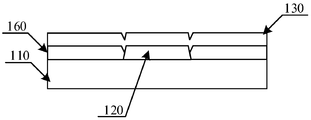
- the reverse pattern can be formed by the patterning process, and the thickness of the reverse pattern is equal to the thickness of the metal pattern 120, that is, the height difference between the area of the metal pattern 120 on the substrate and the other areas can be zero.
- Step 1503 forming an insulating film layer on the substrate on which the reverse pattern is formed such that an overlapping region exists between the insulating film layer and the metal pattern, and an absolute value of a height difference between an overlapping region of the insulating film layer and other regions of the insulating film layer is less than a thickness d.
- FIG. 17 is a schematic view showing the structure of the substrate 110 in which the insulating film layer 130 is formed on the reverse pattern 160, in which the metal pattern 120 is formed on the substrate 110.
- Step 1504 forming a semiconductor layer and a source/drain metal layer pattern on the substrate on which the insulating film layer is formed.
- FIG. 18A is a schematic structural view of a substrate 110 on which a pattern B including a semiconductor layer A and a source and a drain is formed on an insulating film layer 130, wherein a metal pattern formed on the substrate 110 is a pattern 121 of gate lines; and a data line on the substrate
- FIG. 11 is a schematic structural view of a substrate 110 on which a data line 140 is formed on an insulating film layer 130, wherein a metal pattern 120 is formed on the substrate 110.
- the method for fabricating an array substrate is such that the absolute value of the height difference between the overlapping region of the insulating film layer and the other regions of the insulating film layer is smaller than the thickness d, and then on the substrate on which the insulating film layer is formed.
- the undulation of the other patterns formed is correspondingly reduced, and the effect of reducing the disconnection rate of the trace formed on the insulating film layer and improving the yield of the product is achieved.
- FIG. 19A is a schematic diagram of the structure of the source and drain of the array substrate in the prior art and the source and drain structures in the array substrate provided by the embodiment of the present invention.
- the structure 1 is obtained by the method of manufacturing the array substrate shown in FIG. 2
- the structure 2 is obtained by the method of manufacturing the array substrate shown in FIG. 12,
- the structure 3 is obtained by the method of manufacturing the array substrate shown in FIG.
- the structure 1 is the method for manufacturing the array substrate shown in FIG.
- the structure 2 is obtained by the method of manufacturing the array substrate shown in FIG. 7.
- the structure 3 is obtained by the method of manufacturing the array substrate shown in FIG. 12, and the structure 4 is obtained by the method of manufacturing the array substrate shown in FIG. .
- the array substrate manufacturing method provided by the embodiment of the present invention significantly reduces the degree of protrusion of the overlapping regions of the source drain and the pattern of the data lines.
- FIG. 20 is a flowchart illustrating a method of fabricating an array substrate, according to another exemplary embodiment.
- the array substrate manufacturing method can include the following steps:
- step 2001 a trench is formed on the substrate.
- a trench may be first formed on the substrate, and the pattern of the trench may be the same as the metal pattern.
- the substrate may be a glass substrate or other transparent substrate.
- step 2002 a metal pattern having a thickness d is formed in the trench.
- a metal pattern having a thickness d is formed in the trench by a patterning process, for example, 0.1 um ⁇ d ⁇ 0.4 um.
- the metal pattern may be a pattern including gate lines or a pattern including gate lines and common electrode traces, and the metal pattern may be composed of a metal such as Al, Cu or Mo.
- the depth of the trench is equal to the thickness d, it can be considered that the height difference between the overlapping region of the subsequently formed insulating film layer and other regions of the insulating film layer is 0, which can substantially eliminate the metal pattern pair source. The effect of the drain.
- a reverse pattern is formed on the substrate on which the metal pattern is formed such that the reverse pattern is disposed on a region of the substrate where there is no metal pattern, and the reverse pattern is formed of an insulating material.
- a reverse pattern opposite to the metal pattern may be formed on the substrate, and the reverse pattern is disposed on a region of the substrate where there is no metal pattern.
- the insulating material may be an organic material.
- step 2004 an initial insulating film layer is formed on the substrate on which the reverse pattern is formed, wherein an overlapping region of the initial insulating film layer and the metal pattern is convex on the initial insulating film layer.
- an initial insulating film layer may be formed on the substrate on which the reverse pattern is formed, and an overlapping region of the initial insulating film layer and the metal pattern (for example, a gate line) is in the initial insulating film layer Raised up.
- step 2005 the overlapping region of the initial insulating film layer is subjected to a thinning treatment to obtain an insulating film layer such that the absolute value of the height difference between the overlapping region of the insulating film layer and the other regions of the insulating film layer is smaller than the thickness d.
- the overlapping region of the initial insulating film layer may be thinned to obtain an insulating film layer, and the height difference between the overlapping region of the insulating film layer and other regions of the insulating film layer may be absolute. The value is less than the thickness d.
- the overlapping region of the initial insulating film layer may be treated by one patterning process so that the absolute value of the height difference between the overlapping region of the insulating film layer obtained after the treatment and the other regions of the insulating film layer is smaller than the thickness d.
- the height difference between the overlapping region of the initial insulating film layer and other regions of the initial insulating film layer can be controlled by controlling the etching time.
- the height difference between the overlapping region of the insulating film layer obtained after the treatment and the other regions of the insulating film layer may be zero.
- step 2006 a semiconductor layer and a source/drain metal layer pattern are formed on the substrate on which the insulating film layer is formed.
- the semiconductor layer and the source/drain metal layer pattern may be formed on the substrate, and then the substrate is subjected to other subsequent processing.
- the subsequent processing may refer to the prior art as needed. Carry out a detailed description.
- the method for fabricating the array substrate is that the absolute value of the height difference between the overlapping region of the insulating film layer and the other regions of the insulating film layer is smaller than the thickness d, and then The undulations of the other patterns formed on the substrate on which the insulating film layer is formed are correspondingly reduced, and the effect of reducing the disconnection rate of the trace formed on the insulating film layer and improving the yield of the product is achieved.
- FIG. 21 is a schematic structural view showing an array substrate according to an exemplary embodiment.
- the array substrate can include:
- a metal pattern 120 having a thickness d formed on the substrate 110 may be a pattern including gate lines or a pattern including gate lines and common electrode traces;
- the absolute value of the difference x is less than the thickness d;
- a groove is formed on the substrate 110.
- a metal pattern 120 having a thickness d is formed in the trench, and an insulating film layer 130 is formed on the substrate 110 on which the metal pattern 120 is formed.
- the case shown in FIGS. 6A and 6B is a case where the depth of the groove is equal to the thickness of the metal pattern 120, at which time the height difference between the overlapping region of the insulating film layer 130 and the other regions of the insulating film layer 130 is zero.
- the insulating film layer 130 thins the overlapping region of the initial insulating film layer and the metal pattern 120 formed on the substrate 110 on which the metal pattern 120 is formed. Obtained after processing.
- the insulating film layer 130 is obtained by subjecting the overlapping regions of the initial insulating film layer to a patterning process.
- an organic film layer 150, an organic film layer 150 and a metal pattern 120 are formed between the insulating film layer 130 and the substrate 110 on which the metal pattern 120 is formed.
- the insulating film layer 130 is formed on the organic film layer 150 after the thinning treatment of the overlapping region of the organic film layer 150.
- the insulating film layer 130 is exposed and developed at an overlapping region of the organic film layer 150. It is formed on the organic film layer 150 afterwards.
- the substrate 110 on which the metal pattern 120 is formed is formed with a reverse pattern 160, and the reverse pattern 160 is disposed on the substrate 110 without the metal pattern 120.
- the reverse pattern 160 may be formed of an insulating material; the insulating film layer 130 is formed on the substrate 110 on which the reverse pattern 160 is formed, and the insulating film layer 130 and the metal pattern 120 have overlapping regions, and the insulating film layer 130 overlaps.
- the difference in height between the region and the other regions of the insulating film layer 130 is smaller than the thickness d (not shown in FIGS. 18A and 18B).
- the insulating material may be an organic material.
- the overlapping region of the insulating film layer 130 and the metal pattern 120 is zero.
- the array substrate shown in FIG. 21, FIG. 6A, FIG. 6B, FIG. 11, FIG. 14A, FIG. 14B, FIG. 18A, and FIG. 18B may further include the necessary structures of other array substrates, and may be specifically referred to as needed. There are techniques and will not be described in detail here.
- the array substrate provided in this embodiment has an absolute value of the height difference between the overlapping region of the insulating film layer and other regions of the insulating film layer being smaller than the thickness d of the metal pattern, and then forming the substrate of the insulating film layer.
- the undulations of the other patterns formed thereon are correspondingly reduced, and the effect of reducing the disconnection rate of the trace formed on the insulating film layer and improving the yield of the product is achieved.
- FIG. 22 illustrates a display device 2200 that may include the ones shown in FIGS. 21, 6A, 6B, 11, 14A, 14B, 18A, and 18B, according to an exemplary embodiment. Any of the array substrates 2210.
Landscapes
- Thin Film Transistor (AREA)
- Devices For Indicating Variable Information By Combining Individual Elements (AREA)
- Chemical & Material Sciences (AREA)
- Crystallography & Structural Chemistry (AREA)
- Liquid Crystal (AREA)
Abstract
Description
Claims (23)
- 一种阵列基板的制造方法,包括步骤:在基板上形成厚度为d的金属图案;在形成所述金属图案的基板上形成绝缘膜层,使得所述绝缘膜层与所述金属图案存在交叠区域,所述绝缘膜层的交叠区域与所述绝缘膜层的其它区域的高度差的绝对值小于所述厚度d;以及在形成所述绝缘膜层的基板上形成半导体层以及源漏金属层图案。
- 根据权利要求1所述的制造方法,其中,所述在基板上形成厚度为d的金属图案的步骤包括步骤:在所述基板上形成沟槽;以及在所述沟槽中形成所述厚度为d的金属图案。
- 根据权利要求1或2所述的制造方法,其中,所述在形成所述金属图案的基板上形成绝缘膜层的步骤包括步骤:在形成所述金属图案的基板上形成初始绝缘膜层,其中所述初始绝缘膜层与所述金属图案的交叠区域在所述初始绝缘膜层上凸起;以及对所述初始绝缘膜层的交叠区域进行减薄处理以得到所述绝缘膜层,使得所述绝缘膜层的交叠区域与所述绝缘膜层的其它区域的高度差的绝对值小于所述厚度d。
- 根据权利要求3所述的制造方法,其中,所述对所述交叠区域进行减薄处理的步骤包括步骤:通过一次构图工艺对所述初始绝缘膜层的交叠区域进行处理,使处理后的所述初始绝缘膜层的交叠区域与处理后的所述初始绝缘膜层的其它区域的高度差的绝对值小于所述厚度d。
- 根据权利要求1或2所述的制造方法,其中,所述在形成所述金属图案的基板上形成绝缘膜层的步骤包括步骤:在形成所述金属图案的基板上形成有机膜层,其中所述有机膜层与所述金属图案存在交叠区域,所述有机膜层的交叠区域在所述有机膜层上凸起;对所述有机膜层的交叠区域进行减薄处理,使处理后的所述有机膜层的交叠区域与处理后的所述有机膜层的其它区域的高度差的绝对值小于所述厚度d;以及在形成所述有机膜层的基板上形成所述绝缘膜层;或,在形成所述金属图案的基板上形成绝缘的有机膜层,其中所述有机膜层与所述金属图案存在交叠区域,所述有机膜层的交叠区域在所述有机膜层上凸起;以及对所述有机膜层的交叠区域进行减薄处理,使处理后的所述有机膜层的交叠区域与处理后的所述有机膜层的其它区域的高度差的绝对值小于所述厚度d。
- 根据权利要求5所述的制造方法,其中,所述对所述有机膜层的交叠区域进行减薄处理的步骤包括步骤:对所述有机膜层的交叠区域进行曝光显影处理,使处理后的所述有机膜层的交叠区域与处理后的所述有机膜层的其它区域的高度差的绝对值小于所述厚度d。
- 根据权利要求1或2所述的制造方法,其中,所述在形成所述金属图案的基板上形成绝缘膜层的步骤包括步骤:在形成所述金属图案的基板上形成反向图案,使得所述反向图案设置在所述基板上没有所述金属图案的区域,所述反向图案由绝缘材料形成;以及在形成所述反向图案的基板上形成所述绝缘膜层,使得所述绝缘膜层与所述金属图案存在交叠区域,所述绝缘膜层的交叠区域与所述绝缘膜层的其它区域的高度差的绝对值小于所述厚度d。
- 根据权利要求7所述的制造方法,其中,所述绝缘材料为有机材料。
- 根据权利要求7或8所述的制造方法,其中,所述在形成所述反向图案的基板上形成所述绝缘膜层的步骤包括步骤:在形成所述反向图案的基板上形成初始绝缘膜层,其中所述初始绝缘膜层与所述金属图案的交叠区域在所述初始绝缘膜层上凸起;以及对所述初始绝缘膜层的交叠区域进行减薄处理以得到所述绝缘膜层,使得所述绝缘膜层的交叠区域与所述绝缘膜层的其它区域的高度差的绝对值小于所述厚度d。
- 根据权利要求9所述的制造方法,其中,所述对所述交叠区域进行减薄处理的步骤包括步骤:通过一次构图工艺对所述初始绝缘膜层的交叠区域进行处理,使处理后的所述初始绝缘膜层的交叠区域与处理后的所述初始绝缘膜层的其它区域的高度差的绝对值小于所述厚度d。
- 根据权利要求7或8所述的制造方法,其中,所述在形成所述反向图案的基板上形成绝缘膜层的步骤包括步骤:在形成所述反向图案的基板上形成有机膜层,其中所述有机膜层与所述金属图案存在交叠区域,所述有机膜层的交叠区域在所述有机膜层上凸起;对所述有机膜层的交叠区域进行减薄处理,使处理后的所述有机膜层的交叠区域与处理后的所述有机膜层的其它区域的高度差的绝对值小于所述厚度d;以及在形成所述有机膜层的基板上形成所述绝缘膜层;或,在形成所述反向图案的基板上形成绝缘的有机膜层,其中所述有机膜层与所述金属图案存在交叠区域,所述有机膜层的交叠区域在所述有机膜层上凸起;以及对所述有机膜层的交叠区域进行减薄处理,使处理后的所述有机膜层的交叠区域与处理后的所述有机膜层的其它区域的高度差的绝对值小于所述厚度d。
- 根据权利要求11所述的制造方法,其中,所述对所述有机膜层的交叠区域进行减薄处理的步骤包括步骤:对所述有机膜层的交叠区域进行曝光显影处理,使处理后的所述有机膜层的交叠区域与处理后的所述有机膜层的其它区域的高度差的绝对值小于所述厚度d。
- 根据权利要求1至12中任一项所述的制造方法,其中,所述金属图案为包括栅线的图案或包括栅线和公共电极走线的图案。
- 根据权利要求1至13中任一项所述的制造方法,其中,所述绝缘膜层的交叠区域与所述绝缘膜层的其它区域的高度差为0。
- 一种阵列基板,包括:基板;在所述基板上形成的厚度为d的金属图案;在形成所述金属图案的基板上形成的绝缘膜层,其中,所述绝缘膜层与所述金属图案存在交叠区域,所述绝缘膜层的交叠区域与所述绝缘膜层的其它区域的高度差的绝对值小于所述厚度d;以及在所述绝缘膜层上形成的半导体层以及源漏金属层图案。
- 根据权利要求15所述的阵列基板,还包括:在所述基板上形成的沟槽;其中,所述厚度为d的金属图案设置在所述沟槽中。
- 根据权利要求15或16所述的阵列基板,还包括:形成在所述绝缘膜层与所述金属图案之间的有机膜层;其中,所述有机膜层与所述金属图案存在交叠区域。
- 根据权利要求15或16所述的阵列基板,其中所述绝缘膜层为有机的绝缘膜层。
- 根据权利要求15或16所述的阵列基板,还包括:设置在所述绝缘膜层下方的所述基板上没有形成所述金属图案的区域的反向图案,其中,所述反向图案由绝缘材料形成。
- 根据权利要求19所述的阵列基板,其中,所述绝缘材料为有机材料。
- 根据权利要求15至20中任一项所述的阵列基板,其中,所述金属图案为包括栅线的图案或包括栅线和公共电极走线的图案。
- 根据权利要求15至21中任一项所述的阵列基板,其中,所述绝缘膜层的交叠区域与所述绝缘膜层的其它区域的高度差为0。
- 一种显示装置,包括权利要求15至22中任一项所述的阵列基板。
Priority Applications (1)
| Application Number | Priority Date | Filing Date | Title |
|---|---|---|---|
| US14/906,461 US20160240558A1 (en) | 2015-02-12 | 2015-08-18 | Manufacturing method for array substrate, array substrate and display device |
Applications Claiming Priority (2)
| Application Number | Priority Date | Filing Date | Title |
|---|---|---|---|
| CN201510076792.5A CN104795400B (zh) | 2015-02-12 | 2015-02-12 | 阵列基板制造方法、阵列基板和显示装置 |
| CN201510076792.5 | 2015-02-12 |
Publications (1)
| Publication Number | Publication Date |
|---|---|
| WO2016127618A1 true WO2016127618A1 (zh) | 2016-08-18 |
Family
ID=53560093
Family Applications (1)
| Application Number | Title | Priority Date | Filing Date |
|---|---|---|---|
| PCT/CN2015/087337 Ceased WO2016127618A1 (zh) | 2015-02-12 | 2015-08-18 | 阵列基板制造方法、阵列基板和显示装置 |
Country Status (3)
| Country | Link |
|---|---|
| US (1) | US20160240558A1 (zh) |
| CN (1) | CN104795400B (zh) |
| WO (1) | WO2016127618A1 (zh) |
Families Citing this family (5)
| Publication number | Priority date | Publication date | Assignee | Title |
|---|---|---|---|---|
| CN104795400B (zh) * | 2015-02-12 | 2018-10-30 | 合肥鑫晟光电科技有限公司 | 阵列基板制造方法、阵列基板和显示装置 |
| CN110164871A (zh) * | 2019-05-15 | 2019-08-23 | 深圳市华星光电技术有限公司 | Tft阵列基板及其制造方法 |
| CN112533381B (zh) * | 2020-12-01 | 2022-02-15 | 生益电子股份有限公司 | 母板制作方法 |
| CN114815426A (zh) * | 2022-05-10 | 2022-07-29 | 广州华星光电半导体显示技术有限公司 | 阵列基板及显示面板 |
| CN115497960A (zh) * | 2022-08-18 | 2022-12-20 | 广州华星光电半导体显示技术有限公司 | 显示面板及其制备方法与显示装置 |
Citations (6)
| Publication number | Priority date | Publication date | Assignee | Title |
|---|---|---|---|---|
| CN1722934A (zh) * | 2004-07-05 | 2006-01-18 | 精工爱普生株式会社 | 布线形成方法 |
| CN1834740A (zh) * | 2005-03-15 | 2006-09-20 | Nec液晶技术株式会社 | 液晶显示设备及其制造方法 |
| CN103117285A (zh) * | 2013-02-04 | 2013-05-22 | 京东方科技集团股份有限公司 | 一种阵列基板、显示装置及阵列基板的制造方法 |
| CN103489922A (zh) * | 2013-09-30 | 2014-01-01 | 京东方科技集团股份有限公司 | 薄膜晶体管及制备方法、阵列基板及制备方法和显示装置 |
| CN103650149A (zh) * | 2011-08-03 | 2014-03-19 | 松下电器产业株式会社 | 显示面板装置及其制造方法 |
| CN104795400A (zh) * | 2015-02-12 | 2015-07-22 | 合肥鑫晟光电科技有限公司 | 阵列基板制造方法、阵列基板和显示装置 |
Family Cites Families (70)
| Publication number | Priority date | Publication date | Assignee | Title |
|---|---|---|---|---|
| KR950001159B1 (ko) * | 1991-12-27 | 1995-02-11 | 삼성전자 주식회사 | 반도체 메모리장치의 박막트랜지스터 및 그 제조방법 |
| KR950007358B1 (ko) * | 1992-07-01 | 1995-07-10 | 현대전자산업주식회사 | 박막트랜지스터의 제조방법 |
| US5272117A (en) * | 1992-12-07 | 1993-12-21 | Motorola, Inc. | Method for planarizing a layer of material |
| US5532191A (en) * | 1993-03-26 | 1996-07-02 | Kawasaki Steel Corporation | Method of chemical mechanical polishing planarization of an insulating film using an etching stop |
| JP3360350B2 (ja) * | 1993-04-21 | 2002-12-24 | ヤマハ株式会社 | 表面平坦化法 |
| US5356513A (en) * | 1993-04-22 | 1994-10-18 | International Business Machines Corporation | Polishstop planarization method and structure |
| US5726084A (en) * | 1993-06-24 | 1998-03-10 | Northern Telecom Limited | Method for forming integrated circuit structure |
| US5418393A (en) * | 1993-11-29 | 1995-05-23 | Motorola, Inc. | Thin-film transistor with fully gated channel region |
| JPH07245306A (ja) * | 1994-01-17 | 1995-09-19 | Sony Corp | 半導体装置における膜平坦化方法 |
| US5503882A (en) * | 1994-04-18 | 1996-04-02 | Advanced Micro Devices, Inc. | Method for planarizing an integrated circuit topography |
| US5679610A (en) * | 1994-12-15 | 1997-10-21 | Kabushiki Kaisha Toshiba | Method of planarizing a semiconductor workpiece surface |
| DE19712233C2 (de) * | 1996-03-26 | 2003-12-11 | Lg Philips Lcd Co | Flüssigkristallanzeige und Herstellungsverfahren dafür |
| US5705435A (en) * | 1996-08-09 | 1998-01-06 | Industrial Technology Research Institute | Chemical-mechanical polishing (CMP) apparatus |
| US6008505A (en) * | 1997-07-25 | 1999-12-28 | Lg Semicon Co., Ltd. | Thin film transistor and method for fabricating the same |
| KR100259078B1 (ko) * | 1997-08-14 | 2000-06-15 | 김영환 | 박막트랜지스터 및 이의 제조방법 |
| KR100257070B1 (ko) * | 1997-08-14 | 2000-05-15 | 김영환 | 박막트랜지스터 및 이의 제조방법 |
| TW498433B (en) * | 1998-11-16 | 2002-08-11 | Taiwan Semiconductor Mfg | A surface planarization method |
| US6159779A (en) * | 1999-02-03 | 2000-12-12 | Industrial Technology Research Institute | Multi-layer gate for TFT and method of fabrication |
| KR100629174B1 (ko) * | 1999-12-31 | 2006-09-28 | 엘지.필립스 엘시디 주식회사 | 박막트랜지스터 기판 및 그의 제조방법 |
| US6444505B1 (en) * | 2000-10-04 | 2002-09-03 | Industrial Technology Research Institute | Thin film transistor (TFT) structure with planarized gate electrode |
| DE60141225D1 (de) * | 2001-02-19 | 2010-03-18 | Ibm | Verfahren zur herstellung einer dünnfilmtransistorstruktur |
| GB0229191D0 (en) * | 2002-12-14 | 2003-01-22 | Plastic Logic Ltd | Embossing of polymer devices |
| TWI244211B (en) * | 2003-03-14 | 2005-11-21 | Innolux Display Corp | Thin film transistor and method of manufacturing the same and display apparatus using the transistor |
| JP2004343018A (ja) * | 2003-03-20 | 2004-12-02 | Fujitsu Ltd | 半導体装置及びその製造方法 |
| US7037767B2 (en) * | 2003-03-24 | 2006-05-02 | Konica Minolta Holdings, Inc. | Thin-film transistor, thin-film transistor sheet and their manufacturing method |
| KR100973811B1 (ko) * | 2003-08-28 | 2010-08-03 | 삼성전자주식회사 | 유기 반도체를 사용한 박막 트랜지스터 표시판 및 그 제조방법 |
| KR100984359B1 (ko) * | 2003-11-20 | 2010-09-30 | 삼성전자주식회사 | 박막 트랜지스터 표시판 |
| US7297977B2 (en) * | 2004-03-12 | 2007-11-20 | Hewlett-Packard Development Company, L.P. | Semiconductor device |
| US7476572B2 (en) * | 2004-03-25 | 2009-01-13 | Semiconductor Energy Laboratory Co., Ltd. | Method for manufacturing thin film transistor |
| US7223641B2 (en) * | 2004-03-26 | 2007-05-29 | Semiconductor Energy Laboratory Co., Ltd. | Semiconductor device, method for manufacturing the same, liquid crystal television and EL television |
| JP4450834B2 (ja) * | 2004-08-24 | 2010-04-14 | シャープ株式会社 | アクティブマトリクス基板およびそれを備えた表示装置 |
| KR100583972B1 (ko) * | 2004-11-26 | 2006-05-26 | 삼성전자주식회사 | 씨모스 인버터의 노드 콘택 구조체를 갖는 반도체소자의제조방법들 |
| KR20070113893A (ko) * | 2006-05-26 | 2007-11-29 | 삼성전자주식회사 | 유기 절연막 조성물 및 이를 이용하는 이중 두께를 갖는유기 절연막의 제조방법 |
| TWI305682B (en) * | 2006-08-14 | 2009-01-21 | Au Optronics Corp | Bottom substrate for liquid crystal display device and the method of making the same |
| KR101340727B1 (ko) * | 2006-09-11 | 2013-12-12 | 엘지디스플레이 주식회사 | 박막 패턴의 제조방법 및 이를 이용한 액정표시패널 및 그제조방법 |
| US8106386B2 (en) * | 2006-12-28 | 2012-01-31 | Alcatel Lucent | Organic semiconductor compositions including plasticizers |
| US7782413B2 (en) * | 2007-05-09 | 2010-08-24 | Tohoku University | Liquid crystal display device and manufacturing method therefor |
| KR101533098B1 (ko) * | 2008-06-04 | 2015-07-02 | 삼성디스플레이 주식회사 | 박막 트랜지스터 기판 및 그 제조 방법 |
| JP2010080798A (ja) * | 2008-09-29 | 2010-04-08 | Renesas Technology Corp | 半導体集積回路装置および半導体集積回路装置の製造方法 |
| CN101740631B (zh) * | 2008-11-07 | 2014-07-16 | 株式会社半导体能源研究所 | 半导体装置及该半导体装置的制造方法 |
| KR20100067814A (ko) * | 2008-12-12 | 2010-06-22 | 삼성전자주식회사 | 표시 기판 및 이의 제조 방법 |
| US7868391B2 (en) * | 2009-06-04 | 2011-01-11 | International Business Machines Corporation | 3-D single gate inverter |
| WO2011033911A1 (en) * | 2009-09-16 | 2011-03-24 | Semiconductor Energy Laboratory Co., Ltd. | Semiconductor device and manufacturing method thereof |
| US8124463B2 (en) * | 2009-09-21 | 2012-02-28 | International Business Machines Corporation | Local bottom gates for graphene and carbon nanotube devices |
| US8211782B2 (en) * | 2009-10-23 | 2012-07-03 | Palo Alto Research Center Incorporated | Printed material constrained by well structures |
| CN102656698B (zh) * | 2009-12-29 | 2015-06-17 | 夏普株式会社 | 有源矩阵基板及其制造方法 |
| JP5605610B2 (ja) * | 2010-04-23 | 2014-10-15 | セイコーエプソン株式会社 | 有機トランジスタの製造方法 |
| US8592879B2 (en) * | 2010-09-13 | 2013-11-26 | Semiconductor Energy Laboratory Co., Ltd. | Method for manufacturing semiconductor device |
| KR20120061383A (ko) * | 2010-12-03 | 2012-06-13 | 삼성전자주식회사 | 표시 장치 및 그 제조 방법 |
| US8384162B2 (en) * | 2010-12-06 | 2013-02-26 | Institute of Microelectronics, Chinese Academy of Sciences | Device having adjustable channel stress and method thereof |
| KR101283008B1 (ko) * | 2010-12-23 | 2013-07-05 | 주승기 | 트렌치형상의 구리 하부 게이트 구조를 갖는 다결정 실리콘 박막 트랜지스터의 제조방법 |
| KR101637636B1 (ko) * | 2010-12-27 | 2016-07-07 | 샤프 가부시키가이샤 | 액티브 매트릭스 기판 및 그 제조방법, 그리고 표시패널 |
| KR20120075048A (ko) * | 2010-12-28 | 2012-07-06 | 삼성전자주식회사 | 박막 트랜지스터 기판 및 이의 제조 방법 |
| US8809854B2 (en) * | 2011-04-22 | 2014-08-19 | Semiconductor Energy Laboratory Co., Ltd. | Semiconductor device |
| JP5731904B2 (ja) * | 2011-05-25 | 2015-06-10 | ルネサスエレクトロニクス株式会社 | 半導体装置及び半導体装置の製造方法 |
| JP2013016611A (ja) * | 2011-07-04 | 2013-01-24 | Sony Corp | 半導体装置及びその製造方法、並びに、画像表示装置の製造方法 |
| US9490241B2 (en) * | 2011-07-08 | 2016-11-08 | Semiconductor Energy Laboratory Co., Ltd. | Semiconductor device comprising a first inverter and a second inverter |
| US9040981B2 (en) * | 2012-01-20 | 2015-05-26 | Semiconductor Energy Laboratory Co., Ltd. | Semiconductor device |
| TWI493724B (zh) * | 2012-03-01 | 2015-07-21 | E Ink Holdings Inc | 半導體元件 |
| JP2013236068A (ja) * | 2012-04-12 | 2013-11-21 | Semiconductor Energy Lab Co Ltd | 半導体装置及び半導体装置の作製方法 |
| US9059219B2 (en) * | 2012-06-27 | 2015-06-16 | Semiconductor Energy Laboratory Co., Ltd. | Semiconductor device and method for manufacturing semiconductor device |
| CN102790056B (zh) * | 2012-08-13 | 2014-12-10 | 京东方科技集团股份有限公司 | 阵列基板及其制作方法、goa单元制作方法及显示装置 |
| US8946095B2 (en) * | 2012-10-25 | 2015-02-03 | Taiwan Semiconductor Manufacturing Co., Ltd. | Method of forming interlayer dielectric film above metal gate of semiconductor device |
| KR20140061030A (ko) * | 2012-11-13 | 2014-05-21 | 삼성디스플레이 주식회사 | 박막 트랜지스터 표시판 및 그 제조 방법 |
| KR20140095820A (ko) * | 2013-01-25 | 2014-08-04 | 삼성디스플레이 주식회사 | 박막 트랜지스터 기판, 그것의 제조 방법 및 그것을 포함하는 표시 장치 |
| JP2015035506A (ja) * | 2013-08-09 | 2015-02-19 | 株式会社東芝 | 半導体装置 |
| JP2015038925A (ja) * | 2013-08-19 | 2015-02-26 | 株式会社東芝 | 半導体装置 |
| KR102083641B1 (ko) * | 2013-08-29 | 2020-03-03 | 삼성디스플레이 주식회사 | 표시패널 및 이의 제조방법 |
| US9368592B2 (en) * | 2014-01-28 | 2016-06-14 | Taiwan Semiconductor Manufacturing Company Ltd. | Metal gate structure |
| JP3197989U (ja) * | 2015-03-31 | 2015-06-11 | セイコーエプソン株式会社 | 電気光学装置、及び電子機器 |
-
2015
- 2015-02-12 CN CN201510076792.5A patent/CN104795400B/zh not_active Expired - Fee Related
- 2015-08-18 US US14/906,461 patent/US20160240558A1/en not_active Abandoned
- 2015-08-18 WO PCT/CN2015/087337 patent/WO2016127618A1/zh not_active Ceased
Patent Citations (6)
| Publication number | Priority date | Publication date | Assignee | Title |
|---|---|---|---|---|
| CN1722934A (zh) * | 2004-07-05 | 2006-01-18 | 精工爱普生株式会社 | 布线形成方法 |
| CN1834740A (zh) * | 2005-03-15 | 2006-09-20 | Nec液晶技术株式会社 | 液晶显示设备及其制造方法 |
| CN103650149A (zh) * | 2011-08-03 | 2014-03-19 | 松下电器产业株式会社 | 显示面板装置及其制造方法 |
| CN103117285A (zh) * | 2013-02-04 | 2013-05-22 | 京东方科技集团股份有限公司 | 一种阵列基板、显示装置及阵列基板的制造方法 |
| CN103489922A (zh) * | 2013-09-30 | 2014-01-01 | 京东方科技集团股份有限公司 | 薄膜晶体管及制备方法、阵列基板及制备方法和显示装置 |
| CN104795400A (zh) * | 2015-02-12 | 2015-07-22 | 合肥鑫晟光电科技有限公司 | 阵列基板制造方法、阵列基板和显示装置 |
Also Published As
| Publication number | Publication date |
|---|---|
| US20160240558A1 (en) | 2016-08-18 |
| CN104795400B (zh) | 2018-10-30 |
| CN104795400A (zh) | 2015-07-22 |
Similar Documents
| Publication | Publication Date | Title |
|---|---|---|
| KR101901045B1 (ko) | 박막 트랜지스터 및 그 준비 방법, 어레이 기판, 및 디스플레이 장치 | |
| CN103715137A (zh) | 阵列基板及其制造方法、显示装置 | |
| WO2016127618A1 (zh) | 阵列基板制造方法、阵列基板和显示装置 | |
| CN103500730A (zh) | 一种阵列基板及其制作方法、显示装置 | |
| WO2018126636A1 (zh) | 薄膜晶体管、阵列基板和显示装置的制造方法 | |
| CN108231553B (zh) | 薄膜晶体管的制作方法及阵列基板的制作方法 | |
| CN102651322A (zh) | 一种薄膜晶体管及其制造方法、阵列基板、显示器件 | |
| CN106920753A (zh) | 薄膜晶体管及其制作方法、阵列基板和显示器 | |
| JP2014140033A (ja) | 薄膜トランジスタ及びアレイ基板の製造方法 | |
| CN110854205A (zh) | 一种薄膜晶体管及制作方法、显示面板及显示装置 | |
| CN103915450B (zh) | 一种阵列基板、制作方法及显示装置 | |
| WO2015024332A1 (zh) | 显示装置、阵列基板、像素结构及其制造方法 | |
| CN103107140A (zh) | 一种薄膜晶体管阵列基板及其制作方法 | |
| TW201622011A (zh) | 一種垂直型電晶體及其製作方法 | |
| WO2019223076A1 (zh) | 金属氧化物薄膜晶体管及其制作方法、显示器 | |
| CN105226016B (zh) | 阵列基板及其制作方法 | |
| CN105161454B (zh) | 一种阵列基板及其制备方法、显示装置 | |
| CN103383925A (zh) | 显示设备、裸眼3d功能面板的信号基板及其制造方法 | |
| WO2013102370A1 (zh) | 阵列基板及其制造方法以及显示装置 | |
| CN105826329A (zh) | 一种阵列基板的制作方法、阵列基板及液晶面板 | |
| TWI459447B (zh) | 顯示面板及其製作方法 | |
| US11469258B2 (en) | Display panel and display device | |
| CN111584555A (zh) | 阵列基板的制作方法及阵列基板、显示装置 | |
| WO2021027017A1 (zh) | 显示面板及其制作方法 | |
| CN110783204B (zh) | 一种双沟道立体tft器件、显示面板及其制造方法 |
Legal Events
| Date | Code | Title | Description |
|---|---|---|---|
| WWE | Wipo information: entry into national phase |
Ref document number: 14906461 Country of ref document: US |
|
| 121 | Ep: the epo has been informed by wipo that ep was designated in this application |
Ref document number: 15881774 Country of ref document: EP Kind code of ref document: A1 |
|
| NENP | Non-entry into the national phase |
Ref country code: DE |
|
| 32PN | Ep: public notification in the ep bulletin as address of the adressee cannot be established |
Free format text: NOTING OF LOSS OF RIGHTS PURSUANT TO RULE 112(1) EPC (EPO FORM 1205A DATED 08.02.2018) |
|
| 122 | Ep: pct application non-entry in european phase |
Ref document number: 15881774 Country of ref document: EP Kind code of ref document: A1 |