WO2016114072A1 - アーク成膜装置およびアーク成膜方法、ならびに固体蒸発材 - Google Patents
アーク成膜装置およびアーク成膜方法、ならびに固体蒸発材 Download PDFInfo
- Publication number
- WO2016114072A1 WO2016114072A1 PCT/JP2015/085520 JP2015085520W WO2016114072A1 WO 2016114072 A1 WO2016114072 A1 WO 2016114072A1 JP 2015085520 W JP2015085520 W JP 2015085520W WO 2016114072 A1 WO2016114072 A1 WO 2016114072A1
- Authority
- WO
- WIPO (PCT)
- Prior art keywords
- positive electrode
- arc
- positive
- evaporation
- negative electrode
- Prior art date
- Legal status (The legal status is an assumption and is not a legal conclusion. Google has not performed a legal analysis and makes no representation as to the accuracy of the status listed.)
- Ceased
Links
Images






Classifications
-
- C—CHEMISTRY; METALLURGY
- C23—COATING METALLIC MATERIAL; COATING MATERIAL WITH METALLIC MATERIAL; CHEMICAL SURFACE TREATMENT; DIFFUSION TREATMENT OF METALLIC MATERIAL; COATING BY VACUUM EVAPORATION, BY SPUTTERING, BY ION IMPLANTATION OR BY CHEMICAL VAPOUR DEPOSITION, IN GENERAL; INHIBITING CORROSION OF METALLIC MATERIAL OR INCRUSTATION IN GENERAL
- C23C—COATING METALLIC MATERIAL; COATING MATERIAL WITH METALLIC MATERIAL; SURFACE TREATMENT OF METALLIC MATERIAL BY DIFFUSION INTO THE SURFACE, BY CHEMICAL CONVERSION OR SUBSTITUTION; COATING BY VACUUM EVAPORATION, BY SPUTTERING, BY ION IMPLANTATION OR BY CHEMICAL VAPOUR DEPOSITION, IN GENERAL
- C23C14/00—Coating by vacuum evaporation, by sputtering or by ion implantation of the coating forming material
- C23C14/22—Coating by vacuum evaporation, by sputtering or by ion implantation of the coating forming material characterised by the process of coating
- C23C14/24—Vacuum evaporation
-
- C—CHEMISTRY; METALLURGY
- C23—COATING METALLIC MATERIAL; COATING MATERIAL WITH METALLIC MATERIAL; CHEMICAL SURFACE TREATMENT; DIFFUSION TREATMENT OF METALLIC MATERIAL; COATING BY VACUUM EVAPORATION, BY SPUTTERING, BY ION IMPLANTATION OR BY CHEMICAL VAPOUR DEPOSITION, IN GENERAL; INHIBITING CORROSION OF METALLIC MATERIAL OR INCRUSTATION IN GENERAL
- C23C—COATING METALLIC MATERIAL; COATING MATERIAL WITH METALLIC MATERIAL; SURFACE TREATMENT OF METALLIC MATERIAL BY DIFFUSION INTO THE SURFACE, BY CHEMICAL CONVERSION OR SUBSTITUTION; COATING BY VACUUM EVAPORATION, BY SPUTTERING, BY ION IMPLANTATION OR BY CHEMICAL VAPOUR DEPOSITION, IN GENERAL
- C23C14/00—Coating by vacuum evaporation, by sputtering or by ion implantation of the coating forming material
- C23C14/22—Coating by vacuum evaporation, by sputtering or by ion implantation of the coating forming material characterised by the process of coating
- C23C14/24—Vacuum evaporation
- C23C14/32—Vacuum evaporation by explosion; by evaporation and subsequent ionisation of the vapours, e.g. ion-plating
Definitions
- the present invention relates to an arc film forming apparatus, an arc film forming method, and a solid evaporation material.
- a hard film is applied to the surface of the workpiece (that is, the substrate that is the film formation target) using a vacuum arc film formation method.
- Various film forming techniques for forming the film are known.
- an evaporated metal as a film forming material is connected to the negative electrode side of the arc power source, and a vacuum chamber or the like is connected to the positive electrode side of the arc power source.
- a voltage is applied between the evaporated metal on the negative electrode side and the vacuum chamber on the positive electrode side, an arc discharge is generated between them.
- the evaporated metal connected to the negative electrode side evaporates by arc discharge. Metal vapor generated by evaporation adheres to the workpiece. As a result, film formation is performed on the surface of the workpiece.
- the vacuum chamber or the like connected to the positive electrode is heated by the flow of electrons from the evaporated metal on the negative electrode side. Therefore, it is conceivable to use the electron heating to evaporate the film forming material on the positive electrode side and use it for film formation.
- This film forming apparatus includes a vacuum chamber 32 having a space portion 32 a in which a work 33 is accommodated, an arc power source 34, a negative electrode-side evaporated metal 31 connected to the negative electrode side of the arc power source 34, and the arc power source 34.
- a crucible 37 connected to the positive electrode side and a positive electrode side evaporation metal 38 accommodated in the crucible 37 are provided.
- the crucible 37 and the positive electrode side evaporation metal 38 are disposed on the upper surface side of the bottom surface inside the vacuum chamber 32.
- the negative electrode side evaporated metal 31 is disposed on the side wall inside the vacuum chamber 32.
- As the positive electrode side evaporation metal 38 a material having a melting point lower than that of the negative electrode side evaporation metal 31 is used.
- the positive side metal 38 evaporates after being melted in the crucible 37 when heated by receiving electrons from the negative side metal 31.
- a voltage is applied between the negative electrode-side evaporated metal 31 on the negative electrode side of the arc power supply 34 and the crucible 37 on the positive electrode side.
- arc discharge is generated, and the negative electrode-side evaporated metal 31 is evaporated by the arc discharge.
- electrons 39 emitted from the negative electrode-side evaporated metal 31 are generated from magnetic field generating coils 35 and 36 arranged around the negative electrode-side evaporated metal 31 and the crucible 36, respectively, as indicated by an arrow E.
- the magnetic field lines are guided to the positive-side evaporated metal 38.
- the positive side metal 38 is melted in the crucible 37 by the electrons 39 and then evaporated.
- the above-described film forming apparatus shown in FIG. 12 has a configuration in which a crucible 37 and a positive electrode evaporation metal 38 are arranged on the positive electrode side of the arc power supply 34.
- the positive electrode evaporation metal 38 is made of a material having a low melting point and evaporates after passing through a molten state in the crucible 37. Therefore, in order to hold the positive electrode side evaporated metal 8 in the crucible 37 in a molten state, the crucible 37 and the positive electrode evaporation.
- the metal 38 must be placed on the top side of the bottom surface of the vacuum chamber 32 and has significant positional and structural constraints. That is, there is a problem that it is difficult to improve the degree of freedom of installation of the positive electrode side evaporated metal 38.
- An object of the present invention is to provide an arc film forming apparatus and an arc film forming method capable of improving the degree of freedom of installation of the positive electrode side evaporation material.
- An arc film forming apparatus is an arc film forming apparatus for forming a film on the surface of a workpiece using arc discharge, the vacuum chamber accommodating the workpiece, an arc power source having a positive electrode and a negative electrode, and the vacuum Disposed at a position facing the interior of the chamber, connected to the negative electrode side of the arc power source, and disposed at a position facing the interior of the vacuum chamber, and disposed at a position facing the interior of the vacuum chamber.
- a positive-electrode-side evaporation material that is connected to the positive-electrode side and evaporates by electrons emitted from the negative-electrode-side evaporation material, the positive-electrode-side evaporation material is made of a solid, and the solid is heated by hitting the electron It contains a material having a property of sublimating when heated.
- the arc film forming method of the present invention is an arc film forming method for forming a film on the surface of a workpiece using arc discharge, and the negative electrode side evaporation material is disposed at a position facing the inside of the vacuum chamber, and the negative electrode of the arc power source is provided.
- a solid positive-side evaporation material containing a material having a property of sublimation when heated by being hit by electrons is disposed at a position facing the inside of the vacuum chamber and connected to the positive electrode of the arc power source And a step of generating an arc discharge by applying a voltage between the negative electrode and the positive electrode by the arc power source, evaporating the negative electrode-side evaporation material by the arc discharge, and releasing from the negative electrode-side evaporation material
- the positive electrode side evaporating material is sublimated by the generated electrons to evaporate, and the workpiece is formed by the evaporating material generated from the negative electrode side evaporating material and the positive electrode side evaporating material. Characterized in that it comprises and.
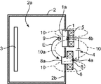
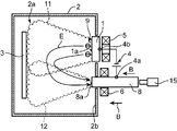
- FIG. 1 is an explanatory cross-sectional view showing an overall configuration of an arc film forming apparatus according to an embodiment of the present invention. It is an enlarged view of the positive electrode evaporation metal of FIG.
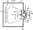
- FIG. 2 is an explanatory cross-sectional view for explaining how electrons move from a negative electrode side evaporation metal to a positive electrode side evaporation metal along magnetic field lines generated from the magnetic field generation coil of FIG. 1. It is sectional explanatory drawing which shows the whole structure of the arc film-forming apparatus which has the structure by which the negative electrode side evaporation metal and positive electrode side evaporation metal which concern on other embodiment of this invention are mutually arrange
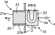
- FIG. 10 is a cross-sectional explanatory view showing another modification of the fixed evaporation material in FIG. 9. It is a schematic sectional drawing which shows the whole structure of the conventional arc film-forming apparatus.
- An arc film forming apparatus (hereinafter referred to as a film forming apparatus) 100 shown in FIG. 1 evaporates the negative electrode-side evaporated metal 1 using arc discharge and uses electrons 9 emitted from the negative electrode-side evaporated metal 1 to positive electrode side. By evaporating the evaporated metal 8, the apparatus performs film formation on the surface of the workpiece 3 (that is, a base material that is a film formation target) by the metal vapors 11 and 12 generated from the metals 1 and 8, respectively.
- the workpiece 3 that is, a base material that is a film formation target
- the film forming apparatus 100 includes a vacuum chamber 2 having a spear space 2a in which a work 3 is accommodated, an arc power source 4 having a positive electrode 4a and a negative electrode 4b, a negative electrode-side evaporated metal 1 connected to the negative electrode 4b side, a positive electrode A positive-side evaporated metal 8 connected to the 4a side, a magnetic field generating coil 5 on the negative electrode 4b side, and a magnetic field generating coil 6 on the positive electrode 4a side are provided.
- the vacuum chamber 2 has a bottom 2d, a side wall 2f extending upward from the bottom 2d, and a top plate 2e positioned above the bottom 2d.
- the side wall 2f has a shape surrounding the space 2a inside the vacuum chamber 2 from the side, and has a plurality of portions facing different directions, specifically, at least the first side wall 2b and the second side facing each other. It has a side wall 2c.
- the space 2a is defined by the bottom 2d, the side wall 2f, and the top plate 2e.
- the pressure of the space 2a is adjusted to a vacuum or a pressure close thereto by a vacuum pump (not shown) during film formation.
- the workpiece 3 is arranged at an arbitrary position inside the space 2a, for example, at a position away from the first side wall 2b by a predetermined distance.
- the negative electrode-side evaporated metal 1 is disposed at a position facing the inside of the vacuum chamber 2, for example, the first side wall 2b.
- the front surface 1 a of the negative electrode-side evaporated metal 1 is exposed inside the space 2 a of the vacuum chamber 2 and faces the workpiece 3.
- the rear surface 1b faces the outside of the vacuum chamber 2 and is connected to the negative electrode 4b.
- the negative electrode side evaporation metal 1 evaporates from the front surface 1a by arc discharge.
- the material of the negative electrode side evaporating metal 1 is selected from materials used for arc vapor plating (hereinafter referred to as AIP), which is a film forming technique that is evaporated by arc discharge and adheres to the surface of the work 3.
- AIP arc vapor plating
- a metal such as chromium is selected.
- the negative electrode side evaporation metal 1 made of a metal material is used as the negative electrode side evaporation material.
- the negative electrode side evaporation material of the present invention is not limited to the metal material, and evaporation other than metal is used. It may be a material (for example, carbon).
- the positive-side evaporated metal 8 is disposed at a position facing the inside of the vacuum chamber 2, for example, at a position in the vicinity of the negative-electrode-side evaporated metal 1 in the first side wall 2b.
- the front surface 8 a of the positive-side evaporated metal 8 is exposed inside the space 2 a of the vacuum chamber 2 and faces the workpiece 3.
- the rear surface 8b faces the outside of the vacuum chamber 2 and is connected to the positive electrode 4a. Note that the negative-side evaporated metal 1 and the positive-side evaporated metal 8 are insulated from each other by the first side wall portion 2 b of the vacuum chamber 2.
- the positive electrode-side evaporated metal 8 evaporates by being heated against the electrons 9 emitted from the negative electrode-side evaporated metal 1.
- the positive electrode-side evaporated metal 8 includes a material having a property of sublimating when heated by being hit by electrons 9.
- the positive-side evaporated metal 8 is heated when the electron 9 hits it under the condition that the pressure inside the vacuum chamber 2 is reduced to a state close to vacuum, for example, under the condition of 0.1 to 10 Pa. Contains materials that have the property of sublimating.
- the sublimation material is at least one material selected from the group consisting of chromium, carbon, magnesium, manganese, molybdenum, nickel, cobalt, silicon, vanadium, and tungsten.
- the sublimation material includes not only a metal material such as chromium but also a non-metal material such as carbon, and preferably has conductivity. Carbon is preferably a semimetal such as graphite because it has conductivity. Note that the above condition of 0.1 to 10 Pa is only an example of selection conditions for the positive electrode-side evaporated metal 8, so that the positive electrode-side evaporated metal 8 can be sublimated even under the above-mentioned conditions of 0.1 to 10 Pa. If it has the property to do, it is contained in the positive electrode side evaporation material of this invention.
- the solid positive electrode-side evaporated metal 8 has a cylindrical shape as shown in FIG. However, the cross-sectional shape of the positive electrode-side evaporated metal 8 can be set to a shape other than a circle.
- the positive electrode-side evaporated metal 8 has a front surface 8a facing the workpiece 3 side.
- the front surface 8a functions as an evaporation surface that generates evaporated metal during film formation.
- the positive-side evaporated metal 8 evaporates with a predetermined length from the front surface 8a as a consumable part 8b.
- the magnetic field generating coil 5 on the negative electrode 4 b side generates a magnetic field 10 that passes through the front surface 1 a of the negative electrode-side evaporated metal 1, and a spot that is hit by arc discharge on the front surface 1 a of the negative electrode-side evaporated metal 1. (Ie, the arc spot) position is controlled.
- the magnetic field generating coil 5 controls the diffusion direction and the diffusion range of the metal vapor 11 that is evaporated and released from the front surface 1a of the negative electrode side evaporation metal 1 during the film formation by the magnetic field 10 described above.
- the magnetic field generating coil 6 on the positive electrode 4a side generates a magnetic field 10 that passes through the front surface 8a of the positive electrode side evaporated metal 8, and is evaporated and emitted from the front surface 8a of the positive electrode side evaporated metal 8 during film formation.
- the diffusion direction and diffusion range of the steam 12 are controlled.
- the two magnetic field generating coils 5 and 6 are controlled so as to generate a magnetic field 10 including a magnetic force line 10 a directed from the negative electrode side evaporated metal 1 to the positive electrode side evaporated metal 8.
- the magnetic field generating coil 6 on the positive electrode 4a side is excited in a direction opposite to the excitation direction of the magnetic field generating coil 5 on the negative electrode 4b side.
- the magnetic force line 10a which connects between the negative electrode side evaporation metal 1 and the positive electrode side evaporation metal 8 as shown in FIG. 3 is formed.
- the lines of magnetic force 10a guide the electrons 9 emitted from the front surface 1a of the negative electrode-side evaporated metal 1 during film formation to the positive electrode-side evaporated metal 8 along the path indicated by the arrow E. Thereby, the electrons 9 are stably guided from the negative electrode side evaporated metal 1 to the positive electrode side evaporated metal 8.
- the magnetic force lines 10a from the negative electrode side evaporated metal 1 to the positive electrode side evaporated metal 8 may be generated only by the negative electrode side magnetic field generating coil 5 in some cases. In such a case, even if the magnetic field generating coil 6 on the positive electrode 4 a side is omitted, the electrons 9 can be stably guided from the negative electrode side evaporated metal 1 to the positive electrode side evaporated metal 8.
- a permanent magnet may be used as another magnetic field generating means instead of these magnetic field generating coils 5 and 6.
- the negative electrode-side evaporated metal 1 is disposed on the inner surface of the first side wall 2b of the vacuum chamber 2 so as to face the inside of the vacuum chamber 2, and is connected to the negative electrode 4b of the arc power source 4.
- a material having a property of sublimation when the electron 9 hits and is heated under the condition that the pressure inside the vacuum chamber 2 is reduced to a state close to vacuum for example, 0.1 to 10 Pa (chromium).
- Etc. is disposed at a position in the vicinity of the negative electrode side evaporation metal 1 of the first side wall 2b as a position facing the inside of the vacuum chamber 2, and is connected to the positive electrode 4a of the arc power source 4. .
- the work 3 is accommodated in the space 2 a of the vacuum chamber 2.
- the air inside the space 2a is evacuated by a vacuum pump (not shown), and the air pressure inside the space 2a is set to a vacuum or a state close thereto.
- an inert gas such as argon is introduced into the space 2 a of the vacuum chamber 2.
- an arc discharge is generated by applying a voltage between the negative electrode 4 b and the positive electrode 4 a by the arc power supply 4, and the negative electrode-side evaporated metal 1 is evaporated by the arc discharge and released from the negative electrode-side evaporated metal 1.
- the positive-side evaporated metal 8 is sublimated by the electrons 9 and evaporated.
- the workpiece 3 is formed by the metal vapor generated by the evaporation of the evaporated metals 1 and 8.
- the positive-side evaporated metal 8 may be supplementarily heated using a heating means such as a heater.
- the positive electrode-side evaporated metal 8 is solid and sublimates when heated by being hit by the electrons 9. Contains materials that have properties. For this reason, the positive-side evaporated metal 8 is sublimated at the time of arc film formation, that is, evaporated from the solid state without passing through the molten state, so that it is not necessary to hold it in the crucible in the molten state. Therefore, the positive-side evaporated metal 8 can be disposed at a place other than the upper surface of the bottom surface of the vacuum chamber 2 and has no restrictions on position and structure. As a result, it is possible to improve the degree of freedom of installation of the positive electrode side evaporated metal 8.
- the positive-side evaporated metal 8 is easily disposed not only on the upper surface of the bottom surface of the vacuum chamber 2, but also on the side wall 2f (specifically, the first side wall portion 2b and the second side wall portion 2c) and the top plate 2e. It becomes possible to do.
- the crucible 37 and the positive electrode side evaporation metal 38 are vacuum chambers so that the molten positive electrode side evaporation metal 38 does not spill from the crucible 37. Since it must be arranged upward on the bottom surface of 32, installation flexibility is limited. In addition, in such a configuration, dust or the like generated on the work surface or the inner surface of the film forming chamber falls during the film forming process and falls into the molten positive electrode-side evaporated metal 38 inside the crucible 37. May affect film quality.
- the positive-side evaporated metal 8 is applied to the side wall 2f (specifically, the first side wall 2b or the second side wall 2c) of the vacuum chamber 2 or the top plate 2e.
- the material to sublimate contained in the positive electrode side evaporation metal 8 is from the group of chromium, carbon, magnesium, manganese, molybdenum, nickel, cobalt, silicon, vanadium, and tungsten. At least one material selected. These materials are materials that form a hard film on the surface of the workpiece 3, and in addition, in the arc film formation, in this embodiment, the pressure inside the vacuum chamber 2 is reduced to a state close to vacuum, For example, under conditions of 0.1 to 10 Pa, it is possible to sublimate when electrons 9 hit and are heated.
- the positive-side evaporated metal 8 is disposed on the first side wall 2b of the vacuum chamber 2, so that the positive-side evaporated metal 8 is formed on the bottom 2d of the vacuum chamber 2. Even when it is difficult to secure the installation space, the positive-side evaporated metal 8 can be easily installed inside the vacuum chamber 2. Even when the positive-side evaporated metal 8 is disposed on the top plate 2e of the vacuum chamber 2, the positive-side evaporated metal 8 can be easily installed even when it is difficult to secure an installation space at the bottom 2d. .
- the negative-electrode-side evaporated metal 1 and the positive-electrode-side evaporated metal 8 are a plurality of portions (the first sidewall portion 2a and the first sidewall portion 2a) that face in different directions on the sidewall 2 of the vacuum chamber 2. Arranged in the same part of the side wall 2b), ie the first side wall 2b. Therefore, it becomes easy to arrange the negative electrode side evaporated metal 1 and the positive electrode side evaporated metal 8 close to each other.
- the path of the electrons 9 from the negative electrode side evaporated metal 1 to the positive electrode side evaporated metal 8 can be shortened, and the positive electrode side evaporated metal 8 can be irradiated with the electrons 9 stably. Further, it is possible to shorten the wiring connecting the negative electrode side evaporated metal 1 and the positive electrode side evaporated metal 8 and the arc power source 4.
- both the negative electrode-side evaporated metal 1 and the positive electrode-side evaporated metal 8 are disposed on the first side wall 2b of the vacuum chamber 2, and the positive electrode-side evaporated metal 8 is negative electrode-side evaporated.
- positions so that it may rank with the metal 1 in the vertical direction
- this invention is not limited to this.
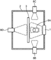
- the position of the positive electrode side evaporation metal 8 with respect to the negative electrode side evaporation metal 1 can be changed freely. For example, as shown in FIG. 4, it may be arranged side by side in the lateral direction (for example, in the horizontal direction) with respect to the negative electrode side evaporated metal 1 as in the positive electrode side evaporated metal 8A.
- the work 3 needs to rotate or revolve around the vertical axis during the film forming process. Thereby, the metal vapor generated from both sides of the negative electrode side evaporated metal 1 and the positive electrode side evaporated metal 8D can be evenly absorbed.
- the arrangement like the positive electrode side evaporated metal 8D is that the work 3 is sandwiched between the negative electrode 1 and the positive electrode side evaporated metal 8D, so that the flow of the electrons 9 is likely to be hindered and arc discharge is difficult to occur. Have a problem. However, this problem can be avoided by appropriately changing the arrangement of the magnetic field lines or the magnetic field, and the arrangement of the work 3, the negative electrode side evaporation metal 1, and the positive electrode side evaporation metal 8D.
- the positive-side evaporated metal 8 and the negative-side evaporated metal 1 are arranged so that one of them surrounds the other. May be.
- the outer negative electrode-side evaporated metal 1 surrounds the inner positive electrode-side evaporated metal 8, and the like with respect to the central axis O 1 of the positive electrode-side evaporated metal 8. It has a configuration arranged at a distance.
- the outer negative-side evaporated metal 1 has a plate shape having an opening in the center.
- the inner positive electrode side evaporation metal 8 has an elongated cylindrical shape and is inserted into the opening of the negative electrode side evaporation metal 1.
- the magnetic field generating coil 5 surrounds the inside of the positive electrode-side evaporated metal 8 and is disposed at a position farther from the workpiece 3 than the outer negative-electrode-side evaporated metal 1 along the axial direction of the positive electrode-side evaporated metal 8. Yes.
- the electrons 9 emitted from the outer negative electrode-side evaporated metal 1 travel along the magnetic field lines generated by the magnetic field generating coil 5 along the path indicated by the arrow E toward the inner positive electrode-side evaporated metal 8. It is possible.
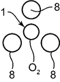
- a plurality of outer positive side evaporation metals 8 surround the inner negative side evaporation metal 1 and the central axis O 2 of the negative side evaporation metal 1 is. May be arranged at an equal distance from each other.
- the outer positive-side evaporated metal 8 has a disc shape or a columnar shape, respectively.
- the inner negative electrode-side evaporated metal 1 has an elongated cylindrical shape and is inserted into the opening of the negative electrode-side evaporated metal 1. Also in this case, similarly to FIG.
- the magnetic field generating coil 5 surrounds the inside of the negative electrode-side evaporated metal 1 and is more than the outer positive-electrode-side evaporated metal 8 along the axial direction of the negative electrode-side evaporated metal 1. It is arranged at a position away from the work 3. At the time of film formation, the electrons 9 emitted from the inner negative electrode side evaporated metal 1 travel along the magnetic field lines generated by the magnetic field generating coil 5 along the path indicated by the arrow E toward the outer positive electrode side evaporated metal 8. It is possible.
- the film forming apparatus further includes a moving unit 15 that moves the positive-side evaporated metal 8 toward the workpiece 3.
- the moving unit 15 has a mechanism that linearly moves the positive-side evaporated metal 8 toward the workpiece 3 in the direction of arrow B.
- the moving unit 15 has a mechanism that includes a mechanism that combines a motor, a pinion gear, and a rack. is doing.
- the moving part 15 causes the positive-side evaporated metal 8 to move away as the positive-side evaporated metal 8 evaporates from the front surface 21 a directed to the workpiece 3 and is consumed during arc film formation. It is possible to advance toward the workpiece 3.
- the front surface 8a of the positive-side evaporated metal 8 can be kept at a fixed position during the film forming process.
- the long positive electrode side evaporated metal 8 is used.
- a film forming apparatus including the moving unit 15 is effective.
- the peripheral surface 21b of the positive-side evaporated metal 21 is covered and the positive-side evaporated metal 21 evaporates from the peripheral surface 21b. Further, an evaporation preventing film 20 may be provided.
- the film forming apparatus shown in FIG. 9 includes the solid evaporated metal 14 having the positive evaporation metal 21 and the evaporation preventing film 20 that covers the peripheral surface 21 b of the positive evaporation metal 21.
- the positive-electrode-side evaporated metal 21 is heated when it is struck by electrons 9 under a reduced pressure state close to a vacuum, for example, under a pressure of 0.1 to 10 Pa. It is a solid evaporated metal containing a material that has the property of sublimating.
- the positive-side evaporated metal 21 has a front surface 21a directed to the workpiece 3, and a peripheral surface 21b that is continuous with the periphery of the front surface 21a and faces a direction different from the front surface 21a.
- the evaporation preventing film 20 covers the peripheral surface 21b of the positive-side evaporated metal 21, and prevents the positive-side evaporated metal 21 from evaporating from the peripheral surface 21b.
- the evaporation prevention film 20 is made of a material such as a metal material or a ceramic having a high melting point as will be described later.
- the evaporation-preventing film 20 covers the peripheral surface 21 b of the positive-side evaporated metal 21, thereby preventing the positive-electrode-side evaporated metal 21 from evaporating from the peripheral surface 21 b. Thereby, it is possible to suppress wasteful consumption of the positive-side evaporated metal 21, and the evaporation material generated from the peripheral surface 21 b of the positive-side evaporated metal 21 is formed around the positive-electrode-side evaporated metal 21. It is possible to reduce the risk of adhering to these components.
- the solid evaporating metal 14 provided with the positive electrode side evaporating metal 21 and the evaporation preventing film 20 can adopt various forms.
- the solid evaporated metal 14 shown in FIG. 10 includes a conductive material in which the evaporation preventing film 20 has a higher melting point than the positive electrode side evaporated metal 21, and the positive electrode side evaporated metal 21 has a rear surface 21 c facing the opposite side of the front surface 21 a.
- the evaporation prevention film 20 has a configuration that further covers the rear surface 21c.
- the evaporation preventing film 20 contains a conductive material having a melting point higher than that of the positive electrode side evaporated metal 21. It is possible to ensure electrical continuity between the metal 21 and the arc power supply 4. Accordingly, the evaporation from the peripheral surface 21b and the rear surface 21c can be prevented by covering the peripheral surface 21b and the rear surface 21c other than the front surface 21a where evaporation is performed in the positive-side evaporated metal 21 with the evaporation preventing film 20. Is possible.
- the evaporation preventing film 20 includes an insulating material, and the positive-side evaporated metal 21 has a rear surface 21c facing the opposite side to the front surface 21a. Further, a contact portion 22 that is in contact with the rear surface 21c of the positive electrode side evaporated metal 21 and has conductivity, and a cooling portion 23 that cools the contact portion 22 may be further included. As described above, when the evaporation preventing film 20 includes an insulating material, it is difficult to ensure electrical continuity between the positive electrode side evaporated metal 21 and the arc power source 4 through the evaporation preventing film 20.
- the contact portion 22 having conductivity contacts the rear surface 21c of the positive-side evaporated metal 21 the above-described electrical conduction can be ensured. Moreover, since the contact part 22 is cooled by the cooling part 23, it is possible to prevent evaporation by cooling the rear surface 21c of the positive electrode side evaporation metal 21 by the contact part 22. As a result, it is possible to evaporate only from the front surface 21a of the positive electrode side evaporation metal 21.
- the solid evaporated metal 14 having the positive electrode side evaporated metal 21 containing the metal material is disclosed as an example of the solid evaporated material of the present invention, but the present invention is not limited to this, It may be a solid evaporation material provided with a positive electrode side evaporation material containing a metal material (for example, carbon) and an evaporation preventing film covering the peripheral surface thereof.
- a metal material for example, carbon
- the film forming apparatus shown in the above embodiment can form a hard film made of various evaporated metals or evaporated metal compounds (compounds of evaporated metal with nitrogen, carbon, oxygen, etc.) on the workpiece surface. . Therefore, by using this film forming apparatus for forming a hard film in order to improve the life and wear sliding characteristics of tools, automobile parts, etc., the film forming speed can be improved, and there is an economic merit.
- the solid evaporating material used in the arc film forming method is described as an example.
- versatility that can be used in other film forming methods.
- the solid evaporation material of the present invention has a front surface directed to the workpiece to be deposited and a peripheral surface that is continuous with the peripheral edge of the front surface and faces in a different direction from the front surface, and is heated in a vacuum or under reduced pressure.
- the arc film forming apparatus of the present embodiment is an arc film forming apparatus that forms a film on the surface of a workpiece using arc discharge, the vacuum chamber that accommodates the workpiece, an arc power source having a positive electrode and a negative electrode, Disposed at a position facing the inside of the vacuum chamber, connected to the negative electrode side of the arc power source, evaporated at the arc discharge, disposed at a position facing the interior of the vacuum chamber, A positive-side evaporation material that is connected to the positive-electrode side and evaporates by electrons emitted from the negative-electrode-side evaporation material, the positive-electrode-side evaporation material is made of a solid, and is heated when the solid hits the electron And a material having a property of sublimating when applied.
- the arc film-forming method of this embodiment is an arc film-forming method in which an arc discharge is used to form a film on the surface of a workpiece, and the negative-side evaporation material is disposed at a position facing the inside of the vacuum chamber,
- a solid positive electrode-side evaporation material including a step of connecting to the negative electrode and a material having a property of sublimation when heated by being hit by electrons is disposed at a position facing the inside of the vacuum chamber, and the positive electrode of the arc power supply
- the positive electrode side evaporation material is sublimated by the emitted electrons to evaporate, and the workpiece is formed by the evaporation material generated from the negative electrode side evaporation material and the positive electrode side evaporation
- the positive electrode-side evaporation material includes a material that is solid and has a property of sublimation when heated by contact with electrons. Therefore, the positive electrode-side evaporating material sublimates during arc film formation, that is, evaporates from the solid state without passing through the molten state, and thus does not need to be held in the crucible in the molten state. Therefore, the positive electrode-side evaporation material can be disposed at a place other than the upper surface of the bottom surface of the vacuum chamber, and has no structural limitation. As a result, it is possible to improve the degree of freedom of installation of the positive electrode side evaporation material.
- the material is preferably at least one material selected from the group consisting of chromium, carbon, magnesium, manganese, molybdenum, nickel, cobalt, silicon, vanadium, and tungsten.
- the above material is a material that forms a hard film on the surface of the workpiece, and can sublimate when heated by being hit by electrons during arc film formation.
- the vacuum chamber includes a bottom portion, a side wall extending upward from the bottom portion, and a top plate positioned above the bottom portion, and the positive-side evaporation material is disposed on the side wall or the top plate. It is preferable.
- the positive side evaporation material can be easily installed inside the vacuum chamber.
- the side wall has a plurality of portions facing in different directions, and the negative electrode side evaporating material and the positive electrode side evaporating material are arranged in the same portion of the plurality of portions. Or it is preferable that the said negative electrode side evaporation material and the said positive electrode side evaporation material are arrange
- the side wall includes a first side wall part and a second side wall part facing each other, the positive side evaporating material is disposed on the first side wall part, and the negative side evaporating material is the second side evaporating material. It is preferable to arrange on the side wall.
- the negative electrode side evaporation material and the positive electrode side evaporation material are arranged so as to face each other with the workpiece interposed therebetween. It is possible to form a film simultaneously from both sides.
- the positive electrode side evaporating material and the negative electrode side evaporating material are arranged so that one of them surrounds the other.
- the positive electrode-side evaporation material has a front surface directed to the workpiece and a peripheral surface that is continuous with a peripheral edge of the front surface and faces a direction different from the front surface
- the arc film forming apparatus includes the positive electrode It is preferable to further include an evaporation preventing film that covers the peripheral surface of the side evaporation material and prevents the positive electrode side evaporation material from evaporating from the peripheral surface.
- the apparatus further includes a moving unit that moves the positive-side evaporation material in a direction approaching the workpiece.
- the positive electrode-side evaporation material evaporates from the front surface directed toward the workpiece and is consumed during arc film formation, so that the moving unit advances the positive-electrode-side evaporation material toward the workpiece, thereby positive electrode It is possible to keep the front surface of the side evaporation material in place.
- the solid evaporation material of the present invention has a front surface directed to a workpiece to be deposited and a peripheral surface that is continuous with the peripheral edge of the front surface and faces a direction different from the front surface, and is heated in vacuum or under reduced pressure.
- the solid evaporating material of the present invention as described above is used as a solid evaporating material in an arc film forming method.
- the solid evaporation material of the present invention includes a front surface directed to a workpiece formed by an arc film forming method using arc discharge, a peripheral surface that is continuous with a peripheral edge of the front surface and faces a direction different from the front surface.
- a solid positive electrode-side evaporating material containing a material having a property of sublimation when heated by being struck with electrons, and covering the peripheral surface of the positive electrode-side evaporating material, wherein the positive electrode-side evaporating material is the peripheral surface And an evaporation preventive film that prevents evaporation from occurring.
- the evaporation prevention film includes a conductive material having a melting point higher than that of the positive electrode-side evaporation material, the positive electrode-side evaporation material has a rear surface facing away from the front surface, and the evaporation prevention film includes the rear surface. Is preferably further covered.
- the evaporation prevention film includes a conductive material having a melting point higher than that of the positive electrode side evaporation material, electrical conduction between the positive electrode evaporation material and the arc power source is ensured through the evaporation prevention film. Is possible. Therefore, it is possible to prevent evaporation from the peripheral surface and the rear surface by covering the peripheral surface and the rear surface other than the front surface where evaporation is performed in the positive-side evaporation material with the evaporation preventing film.
- the evaporation prevention film includes an insulating material, and the positive-side evaporation material has a rear surface facing away from the front surface, contacts the rear surface of the positive-electrode-side evaporation material, and has a conductive contact portion. And a cooling part for cooling the contact part.
- the evaporation prevention film includes an insulating material, it is difficult to ensure electrical continuity between the positive electrode side evaporation material and the arc power source via the evaporation prevention film. It is possible to ensure the electrical continuity described above by bringing a contact portion having conductivity into contact with the rear surface of the material. Further, since the contact portion is cooled by the cooling portion, it is possible to prevent evaporation by cooling the rear surface of the positive electrode side evaporation material by the contact portion. As a result, it is possible to evaporate from only the front surface of the positive electrode side evaporation material.
- the positive electrode side evaporation material can be freely attached to the side wall of the vacuum chamber or the top plate.
- the solid evaporating material of the present invention it is possible to prevent the evaporating material body (specifically, the positive evaporating material in the arc film forming method) from evaporating from the peripheral surface. As a result, it is possible to suppress wasteful consumption of the evaporating material main body, and to reduce the risk of evaporating substances adhering to the components of the film forming apparatus around the evaporating material main body.
- the evaporating material body specifically, the positive evaporating material in the arc film forming method
Landscapes
- Chemical & Material Sciences (AREA)
- Chemical Kinetics & Catalysis (AREA)
- Engineering & Computer Science (AREA)
- Materials Engineering (AREA)
- Mechanical Engineering (AREA)
- Metallurgy (AREA)
- Organic Chemistry (AREA)
- Physical Vapour Deposition (AREA)
Abstract
正極側蒸発材の設置自由度を向上することが可能なアーク成膜装置およびアーク成膜方法を提供する。アーク成膜装置100は、真空チャンバ2内部に面する位置に配置され、アーク電源4の負極4b側に接続され、アーク放電により蒸発する負極側蒸発金属1と、真空チャンバ2内部に面する位置に配置され、アーク電源4の正極4a側に接続され、負極側蒸発金属1から放出される電子によって蒸発する固体の正極側蒸発金属8とを備える。正極側蒸発金属8は、電子が当たって加熱されたときに昇華する性質を有する材料を含んでいる。
Description
本発明は、アーク成膜装置およびアーク成膜方法、ならびに固体蒸発材に関する。
従来より、切削工具や自動車部品などの寿命や摩擦摺動特性等を向上させるために、真空アーク成膜方法を用いてワーク(すなわち、成膜対象物である基材)の表面に硬質の膜を形成する成膜技術が種々知られている。
真空アーク成膜方法では、成膜材料となる蒸発金属がアーク電源の負極側に接続され、真空チャンバなどが当該アーク電源の正極側に接続される。その状態で負極側の蒸発金属と正極側の真空チャンバなどとの間に電圧が印加されることにより、これらの間でアーク放電が発生する。負極側に接続された蒸発金属は、アーク放電によって蒸発する。蒸発によって発生した金属蒸気はワークに付着する。その結果、ワークの表面に成膜が行われる。
このとき、正極に接続された真空チャンバなどは、負極側の蒸発金属から出る電子が流入することによって加熱される。そこで、この電子による加熱を用いて正極側でも成膜材料を蒸発させて成膜に用いることが考えられる。
そのような技術として、図12に示されるように、アーク電源の負極側および正極側の両方において成膜材料となる蒸発金属を蒸発させることが可能な成膜装置が特許文献1に提案されている。この成膜装置は、ワーク33が収容される空間部32aを有する真空チャンバ32と、アーク電源34と、当該アーク電源34の負極側に接続された負極側蒸発金属31と、当該アーク電源34の正極側に接続されたるつぼ37と、るつぼ37に収容された正極側蒸発金属38とを備えている。るつぼ37および正極側蒸発金属38は、真空チャンバ32の内部の底面の上面側に配置されている。負極側蒸発金属31は、真空チャンバ32の内部の側壁に配置されている。正極側蒸発金属38としては、負極側蒸発金属31よりも融点が低い材料が用いられる。正極側蒸発金属38は、負極側蒸発金属31から出る電子を受けて加熱されたときにるつぼ37内で溶融状態を経てから蒸発する。
上記のように構成された成膜装置では、アーク電源34の負極側の負極側蒸発金属31と正極側のるつぼ37との間に電圧が印加される。これによりアーク放電が発生し、そのアーク放電によって負極側蒸発金属31が蒸発する。それとともに、負極側蒸発金属31から放出される電子39は、矢印Eで示されるように、負極側蒸発金属31およびるつぼ36の周囲にそれぞれ配置された磁場発生用のコイル35、36からそれぞれ発生された磁力線によって、正極側蒸発金属38へ案内される。そして、正極側蒸発金属38は、電子39によって、るつぼ37内で溶融し、その後、蒸発する。負極側蒸発金属31および正極側蒸発金属38の蒸発によって発生した2種の金属蒸気がワーク32に付着する。これによって、ワーク32の表面には、負極側蒸発金属31および正極側蒸発金属38を用いた成膜が行われる。このように、1台の真空アーク成膜装置において、アーク電源の正極側および負極側の両極において蒸発金属を蒸発させることにより成膜する事が可能である。
上記のような図12に示される成膜装置は、アーク電源34の正極側にるつぼ37および正極蒸発金属38が配置された構成を有している。正極蒸発金属38は、融点が低い材料からなり、るつぼ37内で溶融状態を経てから蒸発するので、正極側蒸発金属8を溶融状態でるつぼ37内に保持するためには、るつぼ37および正極蒸発金属38は、真空チャンバ32の底面の上面側に配置されなければならず、位置および構造上の著しい制約を有する。すなわち、正極側蒸発金属38の設置自由度の向上が難しいという問題がある。
本発明の目的は、正極側蒸発材の設置自由度を向上することが可能なアーク成膜装置およびアーク成膜方法を提供することを目的とする。
本発明のアーク成膜装置は、アーク放電を用いてワークの表面の成膜を行うアーク成膜装置であって、前記ワークを収容する真空チャンバと、正極および負極を有するアーク電源と、前記真空チャンバ内部に面する位置に配置され、前記アーク電源の前記負極側に接続され、前記アーク放電により蒸発する負極側蒸発材と、前記真空チャンバ内部に面する位置に配置され、前記アーク電源の前記正極側に接続され、前記負極側蒸発材から放出される電子によって蒸発する正極側蒸発材とを備え、前記正極側蒸発材は、固体からなり、かつこの固体が前記電子が当たることにより加熱されたときに昇華する性質を有する材料を含んでいる、ことを特徴とする。
本発明のアーク成膜方法は、アーク放電を用いてワークの表面に成膜を行うアーク成膜方法であって、負極側蒸発材を真空チャンバ内部に面する位置に配置し、アーク電源の負極に接続する工程と、電子が当たって加熱されたときに昇華する性質を有する材料を含む固体の正極側蒸発材を、前記真空チャンバ内部に面する位置に配置し、前記アーク電源の正極に接続する工程と、前記アーク電源によって前記負極と前記正極との間に電圧を印加することによりアーク放電を発生させ、当該アーク放電によって前記負極側蒸発材を蒸発させるとともに、前記負極側蒸発材から放出される電子によって前記正極側蒸発材を昇華させて蒸発させ、前記負極側蒸発材および前記正極側蒸発材から発生した蒸発物質によって前記ワークの成膜を行う工程とを含むことを特徴とする。
以下、図面を参照しながら本発明の実施形態についてさらに詳細に説明する。
図1に示されるアーク成膜装置(以下、成膜装置という)100は、アーク放電を用いて負極側蒸発金属1を蒸発させるとともに負極側蒸発金属1から放出される電子9を用いて正極側蒸発金属8を蒸発させることにより、これらの金属1、8からそれぞれ発生する金属蒸気11、12によってワーク3(すなわち、成膜対象物である基材)の表面の成膜を行う装置である。
この成膜装置100は、ワーク3が収容される 空間部2aを有する真空チャンバ2と、正極4aおよび負極4bを有するアーク電源4と、負極4b側に接続された負極側蒸発金属1と、正極4a側に接続された正極側蒸発金属8と、負極4b側の磁場発生用コイル5と、正極4a側の磁場発生用コイル6とを備えている。
真空チャンバ2は、底部2dと、当該底部2dから上方に延びる側壁2fと、当該底部2dの上方に位置する天板2eとを有している。側壁2fは、真空チャンバ2の内部の空間部2aを側方から囲む形状を有し、異なる方向を向く複数の部分を有し、具体的には少なくとも互いに対向する第1側壁部2bおよび第2側壁部2cを有する。これら底部2d、側壁2f、および天板2eによって前記空間部2aが画定されている。空間部2aの気圧は、成膜時には、図示しない真空ポンプによって真空またはそれに近い気圧に調整される。ワーク3は、空間部2aの内部の任意の位置、例えば、第1側壁部2bから所定の距離だけ離れた位置に配置される。
負極側蒸発金属1は、真空チャンバ2内部に面する位置、例えば、第1側壁部2bに配置されている。負極側蒸発金属1の前面1aは、真空チャンバ2の空間部2a内部に露出してワーク3に向いている。一方、後面1bは、真空チャンバ2の外部を向き、負極4bに接続されている。負極側蒸発金属1は、アーク放電により前面1aから蒸発する。負極側蒸発金属1の材料は、アーク放電によって蒸発されてワーク3表面に付着する成膜技術であるアーク蒸気プレーティング(Arc Ion Plating、以下、AIPという)に用いられる材料が選択され、例えば、クロムなどの金属が選択される。なお、本実施形態では負極側蒸発材として金属材料からなる負極側蒸発金属1が用いられているが、本発明の負極側蒸発材は、金属材料に限定されるものではなく、金属以外の蒸発材料(例えば炭素など)でもよい。
正極側蒸発金属8は、真空チャンバ2内部に面する位置、例えば、第1側壁部2bにおける負極側蒸発金属1の近傍の位置に配置されている。正極側蒸発金属8の前面8aは、真空チャンバ2の空間部2a内部に露出してワーク3に向いている。一方、後面8bは、真空チャンバ2の外部を向き、正極4aに接続されている。なお、負極側蒸発金属1と正極側蒸発金属8との間は、真空チャンバ2の第1側壁部2bによって絶縁されている。
正極側蒸発金属8は、負極側蒸発金属1から放出される電子9に当たって加熱されることによって蒸発する。
正極側蒸発金属8は、電子9が当たって加熱されたときに昇華する性質を有する材料を含んでいる。本実施形態では、正極側蒸発金属8は、真空チャンバ2内部の圧力が真空に近い状態まで減圧した条件下、例えば、0.1~10Paの条件下において電子9が当たって加熱されたときに昇華する性質を有する材料を含んでいる。
具体的には、昇華する材料は、クロム、炭素、マグネシウム、マンガン、モリブデン、ニッケル、コバルト、ケイ素、バナジウム、およびタングステンの群から選ばれた少なくとも1種の材料である。昇華する材料は、クロムなどのような金属材料だけでなく、炭素などの非金属材料も含まれ、導電性を有するのが好ましい。炭素は、黒鉛などの半金属であれば導電性を有するので好ましい。なお、上記の0.1~10Paの条件下は正極側蒸発金属8の選定条件の一例にすぎないので、正極側蒸発金属8は、上記の0.1~10Paの条件下でなくても昇華する性質を有していれば、本発明の正極側蒸発材に含まれる。
固体の正極側蒸発金属8は、図2に示されるような円柱状を有する。しかし、正極側蒸発金属8の断面形状は、円形以外の形状に設定されることも可能である。正極側蒸発金属8は、ワーク3側を向く前面8aを有している。前面8aは、成膜時において蒸発金属を発生する蒸発面として機能する。正極側蒸発金属8は、前面8aから所定の長さ部分を消耗部8bとして蒸発する。
負極4b側の磁場発生用コイル5は、図3に示されるように、負極側蒸発金属1の前面1aを通過する磁場10を発生させ、負極側蒸発金属1の前面1aにおけるアーク放電が当たるスポット(すなわち、アークスポット)の位置を制御する。それととともに、磁場発生用コイル5は、上記の磁場10によって、成膜時に負極側蒸発金属1の前面1aから蒸発して放出される金属蒸気11の拡散方向および拡散範囲を制御する。
同様に、正極4a側の磁場発生用コイル6は、正極側蒸発金属8の前面8aを通過する磁場10を発生させ、成膜時に正極側蒸発金属8の前面8aから蒸発して放出される金属蒸気12の拡散方向および拡散範囲を制御する。
それとともに、上記2つの磁場発生用コイル5、6は、負極側蒸発金属1から正極側蒸発金属8へ向かう磁力線10aを含む磁場10を発生させるように、制御される。具体的には、正極4a側の磁場発生用コイル6は、負極4b側の磁場発生用コイル5の励磁方向とは逆向きに励磁される。これにより、図3に示されるような負極側蒸発金属1と正極側蒸発金属8との間をつなぐ磁力線10aが形成される。この磁力線10aは、成膜時に負極側蒸発金属1の前面1aから放出される電子9を、矢印Eに示される経路に沿って、正極側蒸発金属8へ案内する。これにより、電子9は、負極側蒸発金属1から正極側蒸発金属8へ安定して導かれる。
なお、正極4aおよび負極4bの配置によっては、負極側の磁場発生用コイル5のみで負極側蒸発金属1から正極側蒸発金属8に向かう磁力線10aを発生させることができる場合がある。そのような場合は、正極4a側の磁場発生用コイル6を省略しても、電子9を負極側蒸発金属1から正極側蒸発金属8へ安定して導くことが可能である。
なお、これらの磁場発生用コイル5、6の代わりに他の磁場発生手段として永久磁石が用いられてもよい。
上記のように構成された成膜装置100を用いてアーク成膜方法を行う場合、以下の手順で行われる。
まず、負極側蒸発金属1を、真空チャンバ2内部に面するように真空チャンバ2の第1側壁部2bの内面上に配置し、アーク電源4の負極4bに接続する。
ついで、上記の真空チャンバ2内部の圧力が真空に近い状態まで減圧した条件下、例えば、0.1~10Paの条件下において電子9が当たって加熱されたときに昇華する性質を有する材料(クロムなど)を含む固体の正極側蒸発金属8を、真空チャンバ2内部に面する位置として第1側壁部2bの負極側蒸発金属1の近傍の位置に配置し、アーク電源4の正極4aに接続する。
ついで、真空チャンバ2の空間部2aにワーク3を収容する。そして、空間部2a内部の空気を真空ポンプ(図示せず)によって抜き、空間部2a内部の気圧を真空またはそれに近い状態にする。そののち、真空チャンバ2の空間部2a内部にアルゴンなどの不活性ガスを導入する。
ついで、アーク電源4によって負極4bと正極4aとの間に電圧を印加することによりアーク放電を発生させ、当該アーク放電によって負極側蒸発金属1を蒸発させるとともに、負極側蒸発金属1から放出される電子9によって正極側蒸発金属8を昇華させて蒸発させる。この各蒸発金属1、8の蒸発により発生した金属蒸気によってワーク3の成膜が行われる。
このとき、電子9によって正極側蒸発金属8を加熱させるだけでなく、ヒータ等の加熱手段を用いて正極側蒸発金属8を補助的に加熱してもよい。
以上のように、本実施形態に係るアーク成膜装置100およびそれを用いたアーク成膜方法では、正極側蒸発金属8は、固体であって、電子9が当たって加熱されたときに昇華する性質を有する材料を含んでいる。そのため、正極側蒸発金属8は、アーク成膜時には昇華、すなわち、固体状態から溶融状態を経ずに蒸発するので、溶融状態でるつぼ内に保持する必要がなくなる。そのため、正極側蒸発金属8は、真空チャンバ2の底面の上面以外の場所にも配置することが可能になり、位置および構造上の制約を何ら有しない。その結果、正極側蒸発金属8の設置自由度の向上が可能になる。したがって、正極側蒸発金属8は、真空チャンバ2の底面の上面だけでなく、側壁2f(具体的には、第1側壁部2bや第2側壁部2cなど)や天板2eにも容易に配置することが可能になる。
一方、上述した従来例として図12に示される成膜装置では、溶融状態の正極側蒸発金属38がるつぼ37からこぼれないようにするためには、るつぼ37および正極側蒸発金属38は、真空チャンバ32の底面に上向きに配置せざるを得ないので、設置自由度が制限される。しかも、このような構成では、成膜処理中にワーク表面や成膜チャンバ内面などにおいて生成された塵(ダスト)などが落下してるつぼ37内部の溶融した正極側蒸発金属38に混入して成膜品質に影響を与えるおそれがある。また、塵などがるつぼ37周辺の機械構造物の隙間に入り込むことでるつぼ37側で短絡が生じて正極側蒸発金属38の蒸発に影響を与えるおそれがある。それに対して、本実施形態の成膜装置100では、正極側蒸発金属8を真空チャンバ2の側壁2f(具体的には、第1側壁部2bや第2側壁部2c)や天板2eなどに配置することによって、成膜処理中に生成される塵が正極側蒸発金属8に付着するおそれがなくなり、成膜品質やアーク放電に対する影響のおそれが低減する。
また、本実施形態に係るアーク成膜装置100では、正極側蒸発金属8に含まれる昇華する材料は、クロム、炭素、マグネシウム、マンガン、モリブデン、ニッケル、コバルト、ケイ素、バナジウム、およびタングステンの群から選ばれた少なくとも1種の材料である。これらの材料は、ワーク3の表面に硬質の膜を形成する材料であり、しかも、アーク成膜時において、本実施形態では、真空チャンバ2内部の圧力が真空に近い状態まで減圧した条件下、例えば0.1~10Paの条件下において、電子9が当たって加熱されたときに昇華することが可能である。
さらに、本実施形態に係るアーク成膜装置100では、正極側蒸発金属8は、真空チャンバ2の第1側壁部2bに配置されているので、真空チャンバ2の底部2dに正極側蒸発金属8の設置スペースの確保が難しい場合でも、正極側蒸発金属8を真空チャンバ2の内部に容易に設置することが可能である。なお、正極側蒸発金属8が、真空チャンバ2の天板2eに配置された場合も、底部2dに設置スペースの確保が難しい場合でも、正極側蒸発金属8を容易に設置することが可能である。
さらに、本実施形態に係るアーク成膜装置100では、負極側蒸発金属1および正極側蒸発金属8は、真空チャンバ2の側壁2の異なる方向を向く複数の部分(第1側壁部2aおよび第1側壁部2b)のうちの同じ部分、すなわち第1側壁部2bに配置されている。そのため、負極側蒸発金属1および正極側蒸発金属8を互いに近づけて配置することが容易になる。それによって、負極側蒸発金属1から正極側蒸発金属8へ向かう電子9の道のりを短くすることが可能になり、正極側蒸発金属8へ安定して電子9を照射することが可能である。また、負極側蒸発金属1および正極側蒸発金属8とアーク電源4とを接続する配線を短くすることが可能になる。
なお、上記実施形態の成膜装置100では、負極側蒸発金属1および正極側蒸発金属8が真空チャンバ2の第1側壁部2bにいずれも配置され、かつ、正極側蒸発金属8が負極側蒸発金属1に対して縦方向に並ぶように配置されているが、本発明はこれに限定されるものではない。負極側蒸発金属1に対する正極側蒸発金属8の位置は、自在に変更可能である。例えば、図4に示されるように、正極側蒸発金属8Aのように、負極側蒸発金属1に対して横方向(例えば水平方向)に並べた配置にしてもよい。また、正極側蒸発金属8B、8Cのように、真空チャンバ2の上面および下面にそれぞれ配置してもよい。
さらに、正極側蒸発金属8Dのように真空チャンバ2におけるワークWに対する反対側の面に配置することも可能である。この正極側蒸発金属8Dのような配置にする場合、ワーク3は成膜処理中に垂直軸回りに自転または公転している必要がある。これにより負極側蒸発金属1および正極側蒸発金属8D両側から発生する金属蒸気を均等に吸収することが可能である。また、正極側蒸発金属8Dのような配置にすることは、負極1と正極側蒸発金属8Dとの間にワーク3を挟むので電子9の流れを阻害しやすく、アーク放電がし難くなりやすいという問題を有する。しかし、この問題は、磁力線または磁場の配置、ならびにワーク3、負極側蒸発金属1、および正極側蒸発金属8Dの配置等を適宜変えて設計することによって回避することが可能である。
本発明の成膜装置の他の変形例として、図5~7に示されるように、正極側蒸発金属8および負極側蒸発金属1は、これらのうちの一方が他方の周囲を取り囲むように配置されていてもよい。具体的には、図5に示される成膜装置は、外側の負極側蒸発金属1が内側の正極側蒸発金属8の周囲を取り囲み、当該正極側蒸発金属8の中心軸O1に対して等距離に配置された構成を有する。外側の負極側蒸発金属1は、中央に開口を有する板の形状を有する。一方、内側の正極側蒸発金属8は、細長い円柱形状を有し、負極側蒸発金属1の開口に挿入されている。磁場発生用コイル5は、内側の正極側蒸発金属8の周囲を取り囲み、当該正極側蒸発金属8の軸方向に沿って外側の負極側蒸発金属1よりもワーク3から離れた位置に配置されている。成膜時には、外側の負極側蒸発金属1から放出された電子9は、磁場発生用コイル5によって発生された磁力線に沿って矢印Eで示される経路を通り、内側の正極側蒸発金属8へ向かうことが可能である。
または、図6~7に示される成膜装置のように、外側の複数個の正極側蒸発金属8が内側の負極側蒸発金属1の周囲を取り囲み、当該負極側蒸発金属1の中心軸O2に対して等距離に配置された構成を有するようにしてもよい。外側の正極側蒸発金属8は、それぞれ円板形状または円柱形状を有する。一方、内側の負極側蒸発金属1は、細長い円柱形状を有し、負極側蒸発金属1の開口に挿入されている。この場合も、磁場発生用コイル5は、図5と同様に、内側の負極側蒸発金属1の周囲を取り囲み、当該負極側蒸発金属1の軸方向に沿って外側の正極側蒸発金属8よりもワーク3から離れた位置に配置されている。成膜時には、内側の負極側蒸発金属1から放出された電子9は、磁場発生用コイル5によって発生された磁力線に沿って矢印Eで示される経路を通り、外側の正極側蒸発金属8へ向かうことが可能である。
このように、図5~6に示されるように、正極側蒸発金属8および負極側蒸発金属1が、これらのうちの一方が他方の周囲を取り囲むように配置されている場合、正極側蒸発金属8および負極側蒸発金属1を限られた設置スペースで有効に配置することが可能である。
また、本発明の成膜装置のさらに他の変形例として、図8に示されるように、成膜装置は、正極側蒸発金属8をワーク3へ近づく方向に向かって移動させる移動部15をさらに備えていてもよい。移動部15は、正極側蒸発金属8をワーク3へ向けて矢印Bの方向に直線移動する機構を有しており、例えば、モータとピニオンギヤとラックとを組み合わせた機構などを有する機構などを有している。移動部15を有していることにより、アーク成膜時に正極側蒸発金属8がワーク3に向けられた前面21aから蒸発して消耗するのに合わせて、移動部15が正極側蒸発金属8をワーク3に向かって前進させることが可能である。その結果、成膜処理中は、正極側蒸発金属8の前面8aを定位置に保つことが可能である。
正極側蒸発金属8の消耗量は、負極側蒸発金属1の消耗量よりも多く(数倍程度)であるため、長時間放電を行う場合には上記のような長尺の正極側蒸発金属8および移動部15を備えた成膜装置が有効である。
さらに、本発明の成膜装置のさらに他の変形例として、図9に示されるように、正極側蒸発金属21の周面21bを覆い、正極側蒸発金属21が当該周面21bから蒸発することを防ぐ蒸発防止膜20をさらに備えているようにしてもよい。
すなわち、図9に示される成膜装置は、正極側蒸発金属21および当該正極側蒸発金属21の周面21bを覆う蒸発防止膜20を有する固体蒸発金属14を備えている。
正極側蒸発金属21は、上記の正極側蒸発金属8と同様に、真空に近い状態まで減圧した条件下、例えば圧力が0.1~10Paの条件下において電子9が当たって加熱されたときに昇華する性質を有する材料を含む固体の蒸発金属である。正極側蒸発金属21は、ワーク3に向けられる前面21aと、当該前面21aの周縁に連続し、前面21aと異なる方向を向く周面21bとを有する。
蒸発防止膜20は、正極側蒸発金属21の周面21bを覆い、正極側蒸発金属21が当該周面21bから蒸発することを防ぐ。蒸発防止膜20は、後述するように融点の高い金属材料やセラミックスなどの材料からなる。
図9に示されるように、蒸発防止膜20によって正極側蒸発金属21の周面21bが覆われることにより、正極側蒸発金属21が当該周面21bから蒸発することを防ぐことが可能である。これにより、正極側蒸発金属21の無駄な消耗を抑えることが可能であり、かつ、正極側蒸発金属21の周面21bから発生した蒸発物質が当該正極側蒸発金属21の周囲の成膜装置100の構成部品に付着するおそれを低減することが可能である。
正極側蒸発金属21および蒸発防止膜20を備えた固体蒸発金属14は、種々の形態を採用すること可能である。例えば図10に示される固体蒸発金属14は、蒸発防止膜20が正極側蒸発金属21よりも融点が高い導電材料を含み、正極側蒸発金属21は、前面21aと反対側を向く後面21cを有し、蒸発防止膜20は、後面21cをさらに覆っている構成を有している。
図10に示される固体蒸発金属14を備えた成膜装置では、蒸発防止膜20は正極側蒸発金属21よりも融点が高い導電材料を含んでいるので、蒸発防止膜20を介して正極側蒸発金属21とアーク電源4との電気的な導通を確保することが可能である。したがって、正極側蒸発金属21において蒸発が行われる前面21a以外の部分である周面21bおよび後面21cを蒸発防止膜20で覆うことによって、当該周面21bおよび後面21cからの蒸発を防止することが可能である。
さらに固体蒸発金属14の他の形態としては、図11に示されるように、蒸発防止膜20は、絶縁物質を含み、正極側蒸発金属21は、前面21aと反対側を向く後面21cを有し、正極側蒸発金属21の後面21cに接触し、導電性を有する接触部22と、接触部22を冷却する冷却部23とをさらに含むようにしてもよい。このように蒸発防止膜20が絶縁物質を含む場合には、蒸発防止膜20を介して正極側蒸発金属21とアーク電源4との電気的な導通を確保することが困難である。そこで、正極側蒸発金属21の後面21cに導電性を有する接触部22が接触することにより、上記の電気的な導通を確保することが可能である。また、接触部22は冷却部23によって冷却されるので、当該接触部22によって正極側蒸発金属21の後面21cを冷却して蒸発を防ぐことが可能である。その結果、正極側蒸発金属21の前面21aのみから蒸発させることが可能である。
上記の実施形態では、本発明の固体蒸発材の一例として金属材料を含む正極側蒸発金属21を有する固体蒸発金属14が開示されているが、本発明はこれに限定されるものではなく、非金属材料(例えば炭素など)を含む正極側蒸発材とその周面を覆う蒸発防止膜を備えた固体蒸発材でもよい。
以上の実施形態で示された成膜装置は、種々の蒸発金属または蒸発金属化合物(窒素,炭素,酸素等と蒸発金属の化合物)からなる硬質の膜をワーク表面に形成することが可能である。そのため、この成膜装置を工具や自動車部品等の寿命および摩耗摺動特性向上のために硬質の膜形成に利用することにより、成膜速度を向上させることができ、経済的なメリットがある。
なお、上記図9~11に示される実施形態では、アーク成膜方法に用いられる固体蒸発材を例に挙げて説明しているが、本発明では、他の成膜方法でも利用可能な汎用性の高い固体蒸発材を提案する。すなわち、本発明の固体蒸発材は、成膜されるワークに向けられる前面と、当該前面の周縁に連続し、前記前面と異なる方向を向く周面とを有し、真空中又は減圧下で加熱されたときに昇華する性質を有する材料を含む固体の蒸発材本体と、前記蒸発材本体の前記周面を覆い、前記蒸発材本体が当該周面から蒸発することを防ぐ蒸発防止膜とを備えているものであればよい。このような構成であれば、蒸発防止膜によって蒸発材本体の周面が覆われているので、蒸発材本体が当該周面から蒸発することを防ぐことが可能である。これにより、蒸発材本体の無駄な消耗を抑えることが可能であり、かつ、蒸発材本体の周面から発生した蒸発物質が当該蒸発材本体の周囲の成膜装置の構成部品に付着するおそれを低減することが可能である。
なお、上述した具体的実施形態には以下の構成を有する発明が主に含まれている。
本実施形態のアーク成膜装置は、アーク放電を用いてワークの表面の成膜を行うアーク成膜装置であって、前記ワークを収容する真空チャンバと、正極および負極を有するアーク電源と、前記真空チャンバ内部に面する位置に配置され、前記アーク電源の前記負極側に接続され、前記アーク放電により蒸発する負極側蒸発材と、前記真空チャンバ内部に面する位置に配置され、前記アーク電源の前記正極側に接続され、前記負極側蒸発材から放出される電子によって蒸発する正極側蒸発材とを備え、前記正極側蒸発材は、固体からなり、かつこの固体が前記電子が当たることにより加熱されたときに昇華する性質を有する材料を含んでいる、ことを特徴とする。
本実施形態のアーク成膜方法は、アーク放電を用いてワークの表面に成膜を行うアーク成膜方法であって、負極側蒸発材を真空チャンバ内部に面する位置に配置し、アーク電源の負極に接続する工程と、電子が当たって加熱されたときに昇華する性質を有する材料を含む固体の正極側蒸発材を、前記真空チャンバ内部に面する位置に配置し、前記アーク電源の正極に接続する工程と、前記アーク電源によって前記負極と前記正極との間に電圧を印加することによりアーク放電を発生させ、当該アーク放電によって前記負極側蒸発材を蒸発させるとともに、前記負極側蒸発材から放出される電子によって前記正極側蒸発材を昇華させて蒸発させ、前記負極側蒸発材および前記正極側蒸発材から発生した蒸発物質によって前記ワークの成膜を行う工程とを含むことを特徴とする。
本実施形態のアーク成膜装置およびアーク成膜方法によれば、正極側蒸発材は、固体であって、電子が当たって加 熱されたときに昇華する性質を有する材料を含んでいる。そのため、正極側蒸発材は、アーク成膜時には昇華、すなわち、固体状態から溶融状態を経ずに蒸発するので、溶融状態でるつぼ内に保持する必要がなくなる。そのため、正極側蒸発材は、真空チャンバの底面の上面以外の場所にも配置することが可能になり、構造上の制約を何ら有しない。その結果、正極側蒸発材の設置自由度の向上が可能になる。
また、前記材料は、クロム、炭素、マグネシウム、マンガン、モリブデン、ニッケル、コバルト、ケイ素、バナジウム、およびタングステンの群から選ばれた少なくとも1種の材料であるのが好ましい。
上記の材料は、ワークの表面に硬質の膜を形成する材料であり、しかも、アーク成膜時において、電子が当たって加熱されたときに昇華することが可能である。
また、前記真空チャンバは、底部と、当該底部から上方に延びる側壁と、当該底部の上方に位置する天板とを有しており、前記正極側蒸発材は、前記側壁または前記天板に配置されているのが好ましい。
かかる構成によれば、真空チャンバの底部に正極側蒸発材の設置スペースの確保が難しい場合でも、正極側蒸発材を真空チャンバの内部に容易に設置することが可能である。
また、前記側壁は、異なる方向を向く複数の部分を有しており、前記負極側蒸発材および前記正極側蒸発材は、前記複数の部分のうちの同じ部分に配置されているのが好ましい。または、前記負極側蒸発材および前記正極側蒸発材は、前記天板に配置されているのが好ましい。これらの構成によれば、負極側蒸発材および正極側蒸発材を互いに近づけて配置することが容易になる。それによって、負極側蒸発材から正極側蒸発材へ向かう電子の道のりを短くすることが可能になり、正極側蒸発材へ安定して電子を照射することが可能である。また、負極側蒸発材および正極側蒸発材とアーク電源とを接続する配線を短くすることが可能になる。
また、前記側壁は、互いに対向する第1側壁部および第2側壁部を有しており、前記正極側蒸発材は、前記第1側壁部に配置され、前記負極側蒸発材は、前記第2側壁部に配置されているのが好ましい。
かかる構成によれば、真空チャンバ内部にワークが収容された状態では、負極側蒸発材および正極側蒸発材は、ワークを挟んで向かい合うように配置されるので、これらの蒸発材を用いてワークの両側から同時に成膜を行うことが可能である。
また、前記正極側蒸発材および前記負極側蒸発材は、これらのうちの一方が他方の周囲を取り囲むように配置されているのが好ましい。
かかる構成によれば、正極側蒸発材および負極側蒸発材を限られた設置スペースで有効に配置することが可能である。
また、前記正極側蒸発材は、前記ワークに向けられる前面と、前記前面の周縁に連続し、前記前面と異なる方向を向く周面とを有しており、前記アーク成膜装置は、前記正極側蒸発材の前記周面を覆い、前記正極側蒸発材が当該周面から蒸発することを防ぐ蒸発防止膜をさらに備えているのが好ましい。
かかる構成によれば、蒸発防止膜によって、正極側蒸発材の周面を覆うことにより、正極側蒸発材が当該周面から蒸発することを防ぐことが可能である。これにより、正極側蒸発材の無駄な消耗を抑えることが可能であり、かつ、正極側蒸発材の周面から発生した蒸発物質が当該正極側蒸発材の周囲の成膜装置の構成部品に付着するおそれを低減することが可能である。
また、前記正極側蒸発材を前記ワークへ近づく方向に向かって移動させる移動部をさらに備えているのが好ましい。
かかる構成によれば、アーク成膜時に正極側蒸発材がワークに向けられた前面から蒸発して消耗するのに合わせて、移動部が正極側蒸発材をワークに向かって前進させることにより、正極側蒸発材の前面を定位置に保つことが可能である。
本発明の固体蒸発材は、成膜されるワークに向けられる前面と、当該前面の周縁に連続し、前記前面と異なる方向を向く周面とを有し、真空中又は減圧下で加熱されたときに昇華する性質を有する材料を含む固体の蒸発材本体と、前記蒸発材本体の前記周面を覆い、前記蒸発材本体が当該周面から蒸発することを防ぐ蒸発防止膜とを備えていることを特徴とする。
かかる構成によれば、蒸発防止膜によって蒸発材本体の周面が覆われているので、蒸発材本体が当該周面から蒸発することを防ぐことが可能である。これにより、蒸発材本体の無駄な消耗を抑えることが可能であり、かつ、蒸発材本体の周面から発生した蒸発物質が当該蒸発材本体の周囲の成膜装置の構成部品に付着するおそれを低減することが可能である。
上記のような本発明の固体蒸発材は、アーク成膜方法における固体蒸発材として用いられる。その場合、本発明の固体蒸発材は、アーク放電を用いたアーク成膜方法によって成膜されるワークに向けられる前面と、当該前面の周縁に連続し、前記前面と異なる方向を向く周面とを有し、電子が当たって加熱されたときに昇華する性質を有する材料を含む固体の正極側蒸発材と、前記正極側蒸発材の前記周面を覆い、前記正極側蒸発材が当該周面から蒸発することを防ぐ蒸発防止膜とを備えていることを特徴とする。
かかる構成によれば、蒸発防止膜によって正極側蒸発材の周面が覆われているので、正極側蒸発材が当該周面から蒸発することを防ぐことが可能である。これにより、正極側蒸発材の無駄な消耗を抑えることが可能であり、かつ、正極側蒸発材の周面から発生した蒸発物質が当該正極側蒸発材の周囲の成膜装置の構成部品に付着するおそれを低減することが可能である。
また、前記蒸発防止膜は、前記正極側蒸発材よりも融点が高い導電材料を含み、前記正極側蒸発材は、前記前面と反対側を向く後面を有し、前記蒸発防止膜は、前記後面をさらに覆っているのが好ましい。
かかる構成によれば、蒸発防止膜は正極側蒸発材よりも融点が高い導電材料を含んでいるので、蒸発防止膜を介して正極側蒸発材とアーク電源との電気的な導通を確保することが可能である。したがって、正極側蒸発材において蒸発が行われる前面以外の部分である周面および後面を蒸発防止膜で覆うことによって、当該周面および後面からの蒸発を防止することが可能である。
また、前記蒸発防止膜は、絶縁物質を含み、前記正極側蒸発材は、前記前面と反対側を向く後面を有し、前記正極側蒸発材の前記後面に接触し、導電性を有する接触部と、前記接触部を冷却する冷却部とをさらに含むのが好ましい。
かかる構成によれば、蒸発防止膜が絶縁物質を含む場合には、蒸発防止膜を介して正極側蒸発材とアーク電源との電気的な導通を確保することが困難であるので、正極側蒸発材の後面に導電性を有する接触部を接触することにより、上記の電気的な導通を確保することが可能である。また、接触部は冷却部によって冷却されるので、当該接触部によって正極側蒸発材の後面を冷却して蒸発を防ぐことが可能である。その結果、正極側蒸発材の前面のみから蒸発させることが可能である。
以上説明したように、本発明のアーク成膜装置およびアーク成膜方法によれば、正極側蒸発材の設置自由度を向上することができる。そのため、正極側蒸発材を真空チャンバの側壁や天板などに自在に取り付けることができる。
本発明の固体蒸発材によれば、蒸発材本体(具体的には、アーク成膜方法における正極側蒸発材)がその周面から蒸発することを防ぐことができる。その結果、これにより、蒸発材本体の無駄な消耗を抑えることができ、蒸発材本体の周囲の成膜装置の構成部品に蒸発物質が付着するおそれを低減することができる。
Claims (14)
- アーク放電を用いてワークの表面の成膜を行うアーク成膜装置であって、
前記ワークを収容する真空チャンバと、
正極および負極を有するアーク電源と、
前記真空チャンバ内部に面する位置に配置され、前記アーク電源の前記負極側に接続され、前記アーク放電により蒸発する負極側蒸発材と、
前記真空チャンバ内部に面する位置に配置され、前記アーク電源の前記正極側に接続され、前記負極側蒸発材から放出される電子によって蒸発する正極側蒸発材とを備え、
前記正極側蒸発材は、固体からなり、かつこの固体が前記電子が当たることにより加熱されたときに昇華する性質を有する材料を含んでいる、
アーク成膜装置。 - 前記材料は、クロム、炭素、マグネシウム、マンガン、モリブデン、ニッケル、コバルト、ケイ素、バナジウム、およびタングステンの群から選ばれた少なくとも1種の材料である、
請求項1に記載のアーク成膜装置。 - 前記真空チャンバは、底部と、当該底部から上方に延びる側壁と、当該底部の上方に位置する天板とを有しており、
前記正極側蒸発材は、前記側壁または前記天板に配置されている、
請求項1または2に記載のアーク成膜装置。 - 前記側壁は、異なる方向を向く複数の部分を有しており、
前記負極側蒸発材および前記正極側蒸発材は、前記複数の部分のうちの同じ部分に配置されている、
請求項3に記載のアーク成膜装置。 - 前記負極側蒸発材および前記正極側蒸発材は、前記天板に配置されている、
請求項3に記載のアーク成膜装置。 - 前記側壁は、互いに対向する第1側壁部および第2側壁部を有しており、
前記正極側蒸発材は、前記第1側壁部に配置され、
前記負極側蒸発材は、前記第2側壁部に配置されている、
請求項3に記載のアーク成膜装置。 - 前記正極側蒸発材および前記負極側蒸発材は、これらのうちの一方が他方の周囲を取り囲むように、同軸上に配置されている、
請求項1または2に記載のアーク成膜装置。 - 前記正極側蒸発材は、前記ワークに向けられる前面と、前記前面の周縁に連続し、前記前面と異なる方向を向く周面とを有しており、
前記正極側蒸発材の前記周面を覆い、前記正極側蒸発材が当該周面から蒸発することを防ぐ蒸発防止膜をさらに備えている、
請求項1または2に記載のアーク成膜装置。 - 前記正極側蒸発材を前記ワークへ近づく方向に向かって移動させる移動部をさらに備えている、
請求項1または2に記載のアーク成膜装置。 - アーク放電を用いてワークの表面に成膜を行うアーク成膜方法であって、
負極側蒸発材を真空チャンバ内部に面する位置に配置し、アーク電源の負極に接続する工程と、
電子が当たって加熱されたときに昇華する性質を有する材料を含む固体の正極側蒸発材を、前記真空チャンバ内部に面する位置に配置し、前記アーク電源の正極に接続する工程と、
前記アーク電源によって前記負極と前記正極との間に電圧を印加することによりアーク放電を発生させ、当該アーク放電によって前記負極側蒸発材を蒸発させるとともに、前記負極側蒸発材から放出される電子によって前記正極側蒸発材を昇華させて蒸発させ、前記負極側蒸発材および前記正極側蒸発材から発生した蒸発物質によって前記ワークの成膜を行う工程と
を含むことを特徴とするアーク成膜方法。 - 成膜されるワークに向けられる前面と、当該前面の周縁に連続し、前記前面と異なる方向を向く周面とを有し、真空中又は減圧下で加熱されたときに昇華する性質を有する材料を含む固体の蒸発材本体と、
前記蒸発材本体の前記周面を覆い、前記蒸発材本体が当該周面から蒸発することを防ぐ蒸発防止膜と
を備えた固体蒸発材。 - アーク放電を用いたアーク成膜方法によって成膜されるワークに向けられる前面と、当該前面の周縁に連続し、前記前面と異なる方向を向く周面とを有し、電子が当たって加熱されたときに昇華する性質を有する材料を含む固体の正極側蒸発材と、
前記正極側蒸発材の前記周面を覆い、前記正極側蒸発材が当該周面から蒸発することを防ぐ蒸発防止膜と
を備えた固体蒸発材。 - 前記蒸発防止膜は、前記正極側蒸発材よりも融点が高い導電材料を含み、
前記正極側蒸発材は、前記前面と反対側を向く後面を有し、
前記蒸発防止膜は、前記後面をさらに覆っている、
請求項12に記載の固体蒸発材。 - 前記蒸発防止膜は、絶縁物質を含み、
前記正極側蒸発材は、前記前面と反対側を向く後面を有し、
前記正極側蒸発材の前記後面に接触し、導電性を有する接触部と、
前記接触部を冷却する冷却部と
をさらに含む請求項12に記載の固体蒸発材。
Applications Claiming Priority (2)
| Application Number | Priority Date | Filing Date | Title |
|---|---|---|---|
| JP2015003828A JP2016130330A (ja) | 2015-01-13 | 2015-01-13 | アーク成膜装置およびアーク成膜方法、ならびに固体蒸発材 |
| JP2015-003828 | 2015-01-13 |
Publications (1)
| Publication Number | Publication Date |
|---|---|
| WO2016114072A1 true WO2016114072A1 (ja) | 2016-07-21 |
Family
ID=56405627
Family Applications (1)
| Application Number | Title | Priority Date | Filing Date |
|---|---|---|---|
| PCT/JP2015/085520 Ceased WO2016114072A1 (ja) | 2015-01-13 | 2015-12-18 | アーク成膜装置およびアーク成膜方法、ならびに固体蒸発材 |
Country Status (2)
| Country | Link |
|---|---|
| JP (1) | JP2016130330A (ja) |
| WO (1) | WO2016114072A1 (ja) |
Citations (7)
| Publication number | Priority date | Publication date | Assignee | Title |
|---|---|---|---|---|
| JPH04191360A (ja) * | 1990-11-26 | 1992-07-09 | Asahi Glass Co Ltd | 蒸着方法及びその装置 |
| JPH0625835A (ja) * | 1992-07-09 | 1994-02-01 | Kobe Steel Ltd | 真空蒸着方法及び真空蒸着装置 |
| JPH1068070A (ja) * | 1996-08-26 | 1998-03-10 | Nissin Electric Co Ltd | 化合物膜の形成方法 |
| JP2001058266A (ja) * | 1999-08-18 | 2001-03-06 | Nissin Electric Co Ltd | アーク式蒸発源 |
| JP2003082458A (ja) * | 2001-09-10 | 2003-03-19 | Sumitomo Electric Ind Ltd | 非晶質炭素被膜の形成装置及び形成方法 |
| US20100213054A1 (en) * | 2009-02-24 | 2010-08-26 | Industrial Technology Research Institute | Vacuum coating apparatus with mutiple anodes and film coating method using the same |
| JP2014070226A (ja) * | 2012-09-27 | 2014-04-21 | Ulvac-Riko Inc | 蒸着源および微粒子形成装置 |
-
2015
- 2015-01-13 JP JP2015003828A patent/JP2016130330A/ja active Pending
- 2015-12-18 WO PCT/JP2015/085520 patent/WO2016114072A1/ja not_active Ceased
Patent Citations (7)
| Publication number | Priority date | Publication date | Assignee | Title |
|---|---|---|---|---|
| JPH04191360A (ja) * | 1990-11-26 | 1992-07-09 | Asahi Glass Co Ltd | 蒸着方法及びその装置 |
| JPH0625835A (ja) * | 1992-07-09 | 1994-02-01 | Kobe Steel Ltd | 真空蒸着方法及び真空蒸着装置 |
| JPH1068070A (ja) * | 1996-08-26 | 1998-03-10 | Nissin Electric Co Ltd | 化合物膜の形成方法 |
| JP2001058266A (ja) * | 1999-08-18 | 2001-03-06 | Nissin Electric Co Ltd | アーク式蒸発源 |
| JP2003082458A (ja) * | 2001-09-10 | 2003-03-19 | Sumitomo Electric Ind Ltd | 非晶質炭素被膜の形成装置及び形成方法 |
| US20100213054A1 (en) * | 2009-02-24 | 2010-08-26 | Industrial Technology Research Institute | Vacuum coating apparatus with mutiple anodes and film coating method using the same |
| JP2014070226A (ja) * | 2012-09-27 | 2014-04-21 | Ulvac-Riko Inc | 蒸着源および微粒子形成装置 |
Also Published As
| Publication number | Publication date |
|---|---|
| JP2016130330A (ja) | 2016-07-21 |
Similar Documents
| Publication | Publication Date | Title |
|---|---|---|
| KR20140143352A (ko) | 여과된 음극 아크 증착 장치 및 방법 | |
| US5215640A (en) | Method and arrangement for stabilizing an arc between an anode and a cathode particularly for vacuum coating devices | |
| JP2007100216A (ja) | 蒸発源及びこれを用いた真空蒸着装置 | |
| JP2010525158A (ja) | 真空アーク蒸発源、及び真空アーク蒸発源を有するアーク蒸発チャンバ | |
| KR20250156851A (ko) | 음극 아크 소스 | |
| CN203373418U (zh) | 电子枪装置 | |
| JP2018059134A (ja) | ハースユニット、蒸発源および成膜装置 | |
| JP4810351B2 (ja) | ガス放電による放射線発生装置 | |
| JP4108354B2 (ja) | スパッタリング装置 | |
| WO2016114072A1 (ja) | アーク成膜装置およびアーク成膜方法、ならびに固体蒸発材 | |
| JP5494663B2 (ja) | アーク蒸発源及び真空蒸着装置 | |
| JP3779373B2 (ja) | 真空蒸着装置 | |
| JP2001040467A (ja) | アーク蒸発源、真空蒸着装置及び真空蒸着方法 | |
| JP2017043799A (ja) | ロールトゥロール方式の真空蒸着装置および真空蒸着方法 | |
| EP4195236B1 (en) | Magnetron sputtering apparatus with a movable magnetic field and method of operating the magnetron sputtering apparatus | |
| US20160115585A1 (en) | Apparatus for direct-write sputter deposition and method therefor | |
| US10515785B2 (en) | Cathodic arc deposition apparatus and method | |
| JP2017020056A (ja) | 合金窒化物膜形成装置および合金窒化物膜形成方法 | |
| RU2607398C2 (ru) | Способ нанесения покрытий путем плазменного напыления и устройство для его осуществления | |
| JP6403269B2 (ja) | アーク蒸発源 | |
| WO2013099059A1 (ja) | 成膜装置 | |
| JP5962979B2 (ja) | 成膜装置 | |
| JP2018016836A (ja) | 間接加熱蒸着源 | |
| KR102045209B1 (ko) | 전류제어 마그네트론 적용 pvd 코팅 장치 | |
| JP2001181829A (ja) | アーク式蒸発源 |
Legal Events
| Date | Code | Title | Description |
|---|---|---|---|
| 121 | Ep: the epo has been informed by wipo that ep was designated in this application |
Ref document number: 15878023 Country of ref document: EP Kind code of ref document: A1 |
|
| NENP | Non-entry into the national phase |
Ref country code: DE |
|
| 122 | Ep: pct application non-entry in european phase |
Ref document number: 15878023 Country of ref document: EP Kind code of ref document: A1 |