WO2016110981A1 - 柱状半導体装置と、その製造方法 - Google Patents
柱状半導体装置と、その製造方法 Download PDFInfo
- Publication number
- WO2016110981A1 WO2016110981A1 PCT/JP2015/050391 JP2015050391W WO2016110981A1 WO 2016110981 A1 WO2016110981 A1 WO 2016110981A1 JP 2015050391 W JP2015050391 W JP 2015050391W WO 2016110981 A1 WO2016110981 A1 WO 2016110981A1
- Authority
- WO
- WIPO (PCT)
- Prior art keywords
- layer
- semiconductor
- impurity region
- pillar
- interlayer insulating
- Prior art date
- Legal status (The legal status is an assumption and is not a legal conclusion. Google has not performed a legal analysis and makes no representation as to the accuracy of the status listed.)
- Ceased
Links
Images










Classifications
-
- H—ELECTRICITY
- H10—SEMICONDUCTOR DEVICES; ELECTRIC SOLID-STATE DEVICES NOT OTHERWISE PROVIDED FOR
- H10D—INORGANIC ELECTRIC SEMICONDUCTOR DEVICES
- H10D64/00—Electrodes of devices having potential barriers
- H10D64/20—Electrodes characterised by their shapes, relative sizes or dispositions
- H10D64/23—Electrodes carrying the current to be rectified, amplified, oscillated or switched, e.g. sources, drains, anodes or cathodes
- H10D64/251—Source or drain electrodes for field-effect devices
- H10D64/252—Source or drain electrodes for field-effect devices for vertical or pseudo-vertical devices
-
- H—ELECTRICITY
- H10—SEMICONDUCTOR DEVICES; ELECTRIC SOLID-STATE DEVICES NOT OTHERWISE PROVIDED FOR
- H10D—INORGANIC ELECTRIC SEMICONDUCTOR DEVICES
- H10D30/00—Field-effect transistors [FET]
- H10D30/01—Manufacture or treatment
- H10D30/021—Manufacture or treatment of FETs having insulated gates [IGFET]
- H10D30/025—Manufacture or treatment of FETs having insulated gates [IGFET] of vertical IGFETs
-
- H—ELECTRICITY
- H10—SEMICONDUCTOR DEVICES; ELECTRIC SOLID-STATE DEVICES NOT OTHERWISE PROVIDED FOR
- H10D—INORGANIC ELECTRIC SEMICONDUCTOR DEVICES
- H10D30/00—Field-effect transistors [FET]
- H10D30/60—Insulated-gate field-effect transistors [IGFET]
- H10D30/63—Vertical IGFETs
-
- H—ELECTRICITY
- H10—SEMICONDUCTOR DEVICES; ELECTRIC SOLID-STATE DEVICES NOT OTHERWISE PROVIDED FOR
- H10D—INORGANIC ELECTRIC SEMICONDUCTOR DEVICES
- H10D30/00—Field-effect transistors [FET]
- H10D30/60—Insulated-gate field-effect transistors [IGFET]
- H10D30/791—Arrangements for exerting mechanical stress on the crystal lattice of the channel regions
- H10D30/797—Arrangements for exerting mechanical stress on the crystal lattice of the channel regions being in source or drain regions, e.g. SiGe source or drain
-
- H—ELECTRICITY
- H10—SEMICONDUCTOR DEVICES; ELECTRIC SOLID-STATE DEVICES NOT OTHERWISE PROVIDED FOR
- H10D—INORGANIC ELECTRIC SEMICONDUCTOR DEVICES
- H10D62/00—Semiconductor bodies, or regions thereof, of devices having potential barriers
- H10D62/10—Shapes, relative sizes or dispositions of the regions of the semiconductor bodies; Shapes of the semiconductor bodies
- H10D62/13—Semiconductor regions connected to electrodes carrying current to be rectified, amplified or switched, e.g. source or drain regions
- H10D62/149—Source or drain regions of field-effect devices
- H10D62/151—Source or drain regions of field-effect devices of IGFETs
-
- H—ELECTRICITY
- H10—SEMICONDUCTOR DEVICES; ELECTRIC SOLID-STATE DEVICES NOT OTHERWISE PROVIDED FOR
- H10D—INORGANIC ELECTRIC SEMICONDUCTOR DEVICES
- H10D62/00—Semiconductor bodies, or regions thereof, of devices having potential barriers
- H10D62/10—Shapes, relative sizes or dispositions of the regions of the semiconductor bodies; Shapes of the semiconductor bodies
- H10D62/17—Semiconductor regions connected to electrodes not carrying current to be rectified, amplified or switched, e.g. channel regions
- H10D62/213—Channel regions of field-effect devices
- H10D62/221—Channel regions of field-effect devices of FETs
- H10D62/235—Channel regions of field-effect devices of FETs of IGFETs
- H10D62/292—Non-planar channels of IGFETs
-
- H—ELECTRICITY
- H10—SEMICONDUCTOR DEVICES; ELECTRIC SOLID-STATE DEVICES NOT OTHERWISE PROVIDED FOR
- H10D—INORGANIC ELECTRIC SEMICONDUCTOR DEVICES
- H10D62/00—Semiconductor bodies, or regions thereof, of devices having potential barriers
- H10D62/80—Semiconductor bodies, or regions thereof, of devices having potential barriers characterised by the materials
- H10D62/83—Semiconductor bodies, or regions thereof, of devices having potential barriers characterised by the materials being Group IV materials, e.g. B-doped Si or undoped Ge
-
- H—ELECTRICITY
- H10—SEMICONDUCTOR DEVICES; ELECTRIC SOLID-STATE DEVICES NOT OTHERWISE PROVIDED FOR
- H10D—INORGANIC ELECTRIC SEMICONDUCTOR DEVICES
- H10D64/00—Electrodes of devices having potential barriers
- H10D64/01—Manufacture or treatment
- H10D64/011—Manufacture or treatment of electrodes ohmically coupled to a semiconductor
- H10D64/0111—Manufacture or treatment of electrodes ohmically coupled to a semiconductor to Group IV semiconductors
- H10D64/0112—Manufacture or treatment of electrodes ohmically coupled to a semiconductor to Group IV semiconductors using conductive layers comprising silicides
-
- H—ELECTRICITY
- H10—SEMICONDUCTOR DEVICES; ELECTRIC SOLID-STATE DEVICES NOT OTHERWISE PROVIDED FOR
- H10D—INORGANIC ELECTRIC SEMICONDUCTOR DEVICES
- H10D64/00—Electrodes of devices having potential barriers
- H10D64/20—Electrodes characterised by their shapes, relative sizes or dispositions
- H10D64/27—Electrodes not carrying the current to be rectified, amplified, oscillated or switched, e.g. gates
- H10D64/311—Gate electrodes for field-effect devices
- H10D64/411—Gate electrodes for field-effect devices for FETs
- H10D64/511—Gate electrodes for field-effect devices for FETs for IGFETs
- H10D64/512—Disposition of the gate electrodes, e.g. buried gates
-
- H—ELECTRICITY
- H10—SEMICONDUCTOR DEVICES; ELECTRIC SOLID-STATE DEVICES NOT OTHERWISE PROVIDED FOR
- H10D—INORGANIC ELECTRIC SEMICONDUCTOR DEVICES
- H10D64/00—Electrodes of devices having potential barriers
- H10D64/60—Electrodes characterised by their materials
- H10D64/62—Electrodes ohmically coupled to a semiconductor
-
- H—ELECTRICITY
- H10—SEMICONDUCTOR DEVICES; ELECTRIC SOLID-STATE DEVICES NOT OTHERWISE PROVIDED FOR
- H10D—INORGANIC ELECTRIC SEMICONDUCTOR DEVICES
- H10D84/00—Integrated devices formed in or on semiconductor substrates that comprise only semiconducting layers, e.g. on Si wafers or on GaAs-on-Si wafers
- H10D84/01—Manufacture or treatment
- H10D84/0123—Integrating together multiple components covered by H10D12/00 or H10D30/00, e.g. integrating multiple IGBTs
- H10D84/0126—Integrating together multiple components covered by H10D12/00 or H10D30/00, e.g. integrating multiple IGBTs the components including insulated gates, e.g. IGFETs
- H10D84/0165—Integrating together multiple components covered by H10D12/00 or H10D30/00, e.g. integrating multiple IGBTs the components including insulated gates, e.g. IGFETs the components including complementary IGFETs, e.g. CMOS devices
- H10D84/017—Manufacturing their source or drain regions, e.g. silicided source or drain regions
-
- H—ELECTRICITY
- H10—SEMICONDUCTOR DEVICES; ELECTRIC SOLID-STATE DEVICES NOT OTHERWISE PROVIDED FOR
- H10D—INORGANIC ELECTRIC SEMICONDUCTOR DEVICES
- H10D84/00—Integrated devices formed in or on semiconductor substrates that comprise only semiconducting layers, e.g. on Si wafers or on GaAs-on-Si wafers
- H10D84/01—Manufacture or treatment
- H10D84/0123—Integrating together multiple components covered by H10D12/00 or H10D30/00, e.g. integrating multiple IGBTs
- H10D84/0126—Integrating together multiple components covered by H10D12/00 or H10D30/00, e.g. integrating multiple IGBTs the components including insulated gates, e.g. IGFETs
- H10D84/0165—Integrating together multiple components covered by H10D12/00 or H10D30/00, e.g. integrating multiple IGBTs the components including insulated gates, e.g. IGFETs the components including complementary IGFETs, e.g. CMOS devices
- H10D84/0172—Manufacturing their gate conductors
- H10D84/0177—Manufacturing their gate conductors the gate conductors having different materials or different implants
-
- H—ELECTRICITY
- H10—SEMICONDUCTOR DEVICES; ELECTRIC SOLID-STATE DEVICES NOT OTHERWISE PROVIDED FOR
- H10D—INORGANIC ELECTRIC SEMICONDUCTOR DEVICES
- H10D84/00—Integrated devices formed in or on semiconductor substrates that comprise only semiconducting layers, e.g. on Si wafers or on GaAs-on-Si wafers
- H10D84/01—Manufacture or treatment
- H10D84/0123—Integrating together multiple components covered by H10D12/00 or H10D30/00, e.g. integrating multiple IGBTs
- H10D84/0126—Integrating together multiple components covered by H10D12/00 or H10D30/00, e.g. integrating multiple IGBTs the components including insulated gates, e.g. IGFETs
- H10D84/0165—Integrating together multiple components covered by H10D12/00 or H10D30/00, e.g. integrating multiple IGBTs the components including insulated gates, e.g. IGFETs the components including complementary IGFETs, e.g. CMOS devices
- H10D84/0195—Integrating together multiple components covered by H10D12/00 or H10D30/00, e.g. integrating multiple IGBTs the components including insulated gates, e.g. IGFETs the components including complementary IGFETs, e.g. CMOS devices the components including vertical IGFETs
-
- H—ELECTRICITY
- H10—SEMICONDUCTOR DEVICES; ELECTRIC SOLID-STATE DEVICES NOT OTHERWISE PROVIDED FOR
- H10D—INORGANIC ELECTRIC SEMICONDUCTOR DEVICES
- H10D84/00—Integrated devices formed in or on semiconductor substrates that comprise only semiconducting layers, e.g. on Si wafers or on GaAs-on-Si wafers
- H10D84/01—Manufacture or treatment
- H10D84/02—Manufacture or treatment characterised by using material-based technologies
- H10D84/03—Manufacture or treatment characterised by using material-based technologies using Group IV technology, e.g. silicon technology or silicon-carbide [SiC] technology
- H10D84/038—Manufacture or treatment characterised by using material-based technologies using Group IV technology, e.g. silicon technology or silicon-carbide [SiC] technology using silicon technology, e.g. SiGe
-
- H—ELECTRICITY
- H10—SEMICONDUCTOR DEVICES; ELECTRIC SOLID-STATE DEVICES NOT OTHERWISE PROVIDED FOR
- H10D—INORGANIC ELECTRIC SEMICONDUCTOR DEVICES
- H10D84/00—Integrated devices formed in or on semiconductor substrates that comprise only semiconducting layers, e.g. on Si wafers or on GaAs-on-Si wafers
- H10D84/80—Integrated devices formed in or on semiconductor substrates that comprise only semiconducting layers, e.g. on Si wafers or on GaAs-on-Si wafers characterised by the integration of at least one component covered by groups H10D12/00 or H10D30/00, e.g. integration of IGFETs
- H10D84/82—Integrated devices formed in or on semiconductor substrates that comprise only semiconducting layers, e.g. on Si wafers or on GaAs-on-Si wafers characterised by the integration of at least one component covered by groups H10D12/00 or H10D30/00, e.g. integration of IGFETs of only field-effect components
- H10D84/83—Integrated devices formed in or on semiconductor substrates that comprise only semiconducting layers, e.g. on Si wafers or on GaAs-on-Si wafers characterised by the integration of at least one component covered by groups H10D12/00 or H10D30/00, e.g. integration of IGFETs of only field-effect components of only insulated-gate FETs [IGFET]
- H10D84/85—Complementary IGFETs, e.g. CMOS
-
- H—ELECTRICITY
- H10—SEMICONDUCTOR DEVICES; ELECTRIC SOLID-STATE DEVICES NOT OTHERWISE PROVIDED FOR
- H10D—INORGANIC ELECTRIC SEMICONDUCTOR DEVICES
- H10D88/00—Three-dimensional [3D] integrated devices
-
- H—ELECTRICITY
- H10—SEMICONDUCTOR DEVICES; ELECTRIC SOLID-STATE DEVICES NOT OTHERWISE PROVIDED FOR
- H10D—INORGANIC ELECTRIC SEMICONDUCTOR DEVICES
- H10D88/00—Three-dimensional [3D] integrated devices
- H10D88/01—Manufacture or treatment
-
- H—ELECTRICITY
- H10—SEMICONDUCTOR DEVICES; ELECTRIC SOLID-STATE DEVICES NOT OTHERWISE PROVIDED FOR
- H10P—GENERIC PROCESSES OR APPARATUS FOR THE MANUFACTURE OR TREATMENT OF DEVICES COVERED BY CLASS H10
- H10P14/00—Formation of materials, e.g. in the shape of layers or pillars
- H10P14/40—Formation of materials, e.g. in the shape of layers or pillars of conductive or resistive materials
- H10P14/42—Formation of materials, e.g. in the shape of layers or pillars of conductive or resistive materials using a gas or vapour
- H10P14/44—Physical vapour deposition [PVD]
-
- H—ELECTRICITY
- H10—SEMICONDUCTOR DEVICES; ELECTRIC SOLID-STATE DEVICES NOT OTHERWISE PROVIDED FOR
- H10D—INORGANIC ELECTRIC SEMICONDUCTOR DEVICES
- H10D30/00—Field-effect transistors [FET]
- H10D30/01—Manufacture or treatment
- H10D30/021—Manufacture or treatment of FETs having insulated gates [IGFET]
- H10D30/0212—Manufacture or treatment of FETs having insulated gates [IGFET] using self-aligned silicidation
-
- H—ELECTRICITY
- H10—SEMICONDUCTOR DEVICES; ELECTRIC SOLID-STATE DEVICES NOT OTHERWISE PROVIDED FOR
- H10D—INORGANIC ELECTRIC SEMICONDUCTOR DEVICES
- H10D84/00—Integrated devices formed in or on semiconductor substrates that comprise only semiconducting layers, e.g. on Si wafers or on GaAs-on-Si wafers
- H10D84/01—Manufacture or treatment
- H10D84/0123—Integrating together multiple components covered by H10D12/00 or H10D30/00, e.g. integrating multiple IGBTs
- H10D84/0126—Integrating together multiple components covered by H10D12/00 or H10D30/00, e.g. integrating multiple IGBTs the components including insulated gates, e.g. IGFETs
- H10D84/0165—Integrating together multiple components covered by H10D12/00 or H10D30/00, e.g. integrating multiple IGBTs the components including insulated gates, e.g. IGFETs the components including complementary IGFETs, e.g. CMOS devices
- H10D84/0172—Manufacturing their gate conductors
Definitions
- the present invention relates to a columnar semiconductor device and a manufacturing method thereof.
- SGT Shorting Gate MOS Transistor
- the channel exists in the horizontal direction along the upper surface of the semiconductor substrate.
- the channel of SGT exists in the direction perpendicular
- FIG. 7 shows a structural schematic diagram of an N-channel SGT.
- Si pillars When one of the Si pillars 100 (hereinafter referred to as “silicon pillars”) having a P-type or i-type (intrinsic) conductivity type (hereinafter referred to as “Si pillar”) is a source, the other is a drain.
- N + regions 101a and 101b hereinafter, a semiconductor region containing a high concentration of donor impurities is referred to as an “N + region”.
- the Si pillar 100 between the N + regions 101 a and 101 b serving as the source and drain becomes the channel region 102.
- a gate insulating layer 103 is formed so as to surround the channel region 102, and a gate conductor layer 104 is formed so as to surround the gate insulating layer 103.
- N + regions 101 a and 101 b that become sources and drains, a channel region 102, a gate insulating layer 103, and a gate conductor layer 104 are formed in a single Si pillar 100.
- the area of the SGT in plan view corresponds to the area of a single source or drain N + region of the planar MOS transistor. Therefore, the circuit chip having SGT can realize further reduction of the chip size as compared with the circuit chip having a planar type MOS transistor.
- the circuit area can be reduced by forming two SGTs 116 a and 116 b at the upper and lower positions of one Si pillar 115.
- FIG. 8 is a schematic structural diagram of a circuit in which an N channel SGT 116a is formed below the Si pillar 115 and a P channel SGT 116b is formed above the N channel SGT 116a.
- Si pillar 115 is formed on P layer substrate 117 (hereinafter, a semiconductor layer containing acceptor impurities is referred to as “P layer”).
- An SiO 2 layer 118 is formed on the outer periphery of the Si pillar 115 and on the P layer substrate 117.
- a gate insulating layer 119a of the N channel SGT 116a and a gate insulating layer 119b of the P channel SGT 116b are formed so as to surround the Si pillar 115.
- a gate conductor layer 120a of the N-channel SGT 116a and a gate conductor layer 120b of the P-channel SGT 116b are formed on the outer periphery of the Si pillar 115 so as to surround the gate insulating layers 119a and 119b.
- An N + region 121 a is formed in the surface layer portion of the P layer substrate 117 connected to the bottom portion of the Si pillar 115.
- an N + region 121b, an SiO 2 layer 130 connected to the N + region 121b, and a P + region 122a connected to the SiO 2 layer 130 (hereinafter, containing an acceptor impurity at a high concentration).
- the semiconductor region is referred to as a “P + region”.
- a P + region 122 b is formed at the top of the Si pillar 115.
- the N + region 121a is the source of the N channel SGT 116a, and the N + region 121b is the drain of the N channel SGT 116a.
- Si pillar 115 between N + regions 121a and 121b is channel region 123a of N channel SGT 116a.
- the P + region 122b is the drain of the P channel SGT 116b, and the P + region 122a is the source of the P channel SGT 116b.
- Si pillar 115 between P + regions 122a and 122b is channel region 123b of P channel SGT 116b.
- a nickel silicide layer (NiSi layer) 125 a is formed on the surface layer portion of the N + region 121 a connected to the bottom of the Si pillar 115.
- a NiSi layer 125b is formed on the outer periphery of the N + region 121b in the central portion of the Si pillar 115
- a NiSi layer 125c is formed on the outer periphery of the P + region 122a, and the upper surface layer of the P + region 122b on the top of the Si pillar 115 is formed.
- a NiSi layer 125d is formed.
- a source wiring metal layer 126a is formed so as to be connected to the NiSi layer 125a in the N + region 121a, and the source wiring metal layer 126a is connected to the VS1 terminal.
- a drain wiring metal layer 126b is formed so as to be connected to the NiSi layer 125b, and the drain wiring metal layer 126b is connected to the drain terminal VD1.
- a source wiring metal layer 126c is formed so as to be connected to the NiSi layer 125c in the P + region 122a, and the source wiring metal layer 126c is connected to the VS2 terminal.
- a drain wiring metal layer 126d is formed so as to be connected to the NiSi layer 125d, and the drain wiring metal layer 126d is connected to the VD2 terminal.
- Gate wiring metal layers 127a and 127b are formed so as to be connected to the gate conductor layers 120a and 120b, and the gate wiring metal layers 127a and 127b are connected to gate terminals VG1 and VG2, respectively. Thereby, two SGTs 116 a and 116 b separated by the SiO 2 layer 130 are formed on the Si pillar 115.
- the linear thermal expansion coefficient of NiSi (12 ⁇ 10 ⁇ 6 / K) and the linear thermal expansion coefficient of Si (2.4 ⁇ 10 ⁇ 6 / K) It is difficult to prevent the Si pillar 115 from bending or falling due to the difference.
- NiSi layers 125b and 125c are accurately and easily formed on the outer periphery of the N + region 121b and the P + region 122a, 3.
- the connection between the NiSi layer 125b and the drain wiring metal layer 126b, and the connection between the NiSi layer 125c and the source wiring metal layer 126c are accurately and easily formed. 4).
- the linear thermal expansion coefficient of NiSi (12 ⁇ 10 ⁇ 6 / K) and the linear thermal expansion coefficient of Si (2.4 ⁇ 10 ⁇ 6 / K) It is required to prevent the Si pillar 115 from bending or falling due to the difference.
- a columnar semiconductor device is: On a semiconductor substrate, a semiconductor pillar standing in a direction perpendicular to the semiconductor substrate plane; A first interlayer insulating layer formed in the semiconductor pillar; A first impurity region containing donor or acceptor atoms formed in the semiconductor pillar and in contact with the first interlayer insulating layer and below the first interlayer insulating layer; A second impurity region containing donor or acceptor atoms formed in the semiconductor pillar and in contact with the first interlayer insulating layer and above the first interlayer insulating layer; A first alloy layer in contact with a side surface of the first impurity region and formed in the semiconductor pillar and an outer periphery of the semiconductor pillar; A second alloy layer that is in contact with the side surface of the second impurity region and is formed in the semiconductor pillar and on the outer periphery of the semiconductor pillar; A second interlayer insulating layer between the first alloy layer and the second alloy layer and having a side surface formed away from the semiconductor
- the semiconductor pillar standing in a direction perpendicular to the semiconductor substrate plane; A gate insulating layer surrounding the semiconductor pillar; A gate conductor layer surrounding the gate insulating layer; A third impurity region formed at the bottom of the semiconductor pillar and having the same conductivity as the first impurity region; A fourth impurity region in the semiconductor pillar above the second impurity region and having the same conductivity as the second impurity region; A third interlayer insulating layer in contact with the lower surface of the first alloy layer; A fourth interlayer insulating layer in contact with the upper surface of the second alloy layer; One of the first impurity region and the third impurity region is a source, the other is a drain, a portion of the semiconductor pillar between the first impurity region and the third impurity region is a channel,
- the gate conductor layer functions as a gate to form a first SGT (Surrounding Gate MOS Transistor), One of the second impurity region and the fourth impurity region serves as a source, the
- the first alloy layer and the second alloy layer are formed to the center of the semiconductor pillar in a plan view. It is desirable.
- the first alloy layer and the second alloy layer are wiring conductor material layers, It is desirable.
- the first alloy layer and the second alloy layer pass through the second alloy layer and the second interlayer insulating layer, and the bottom is on the upper surface, the inside, or the lower surface of the first alloy layer. It is connected to the wiring metal layer formed on the upper part of the contact hole through the contact hole that reaches, It is desirable.
- stress is formed downward from the fourth impurity region. It is desirable.
- a space is provided between the first alloy layer, the second alloy layer, and the gate conductor layer. It is desirable.
- a method for manufacturing a columnar semiconductor device includes: A semiconductor pillar forming step of forming a semiconductor pillar on the semiconductor substrate in a direction perpendicular to the semiconductor substrate plane and having a first interlayer insulating layer therein; The first metal layer, the first semiconductor layer containing donor or acceptor atoms, and the first interlayer insulating layer in the vertical direction at the outer periphery of the semiconductor pillar and away from the side face of the semiconductor pillar.
- a second interlayer insulating layer at a height, a second metal layer, a second semiconductor layer containing donor or acceptor atoms, and a third interlayer insulating layer are arranged in a direction perpendicular to the plane of the semiconductor substrate.
- the semiconductor column includes a first impurity region in contact with the first alloy layer and a second impurity region in contact with the second alloy layer, which includes the donor or acceptor atom. Alloy layer / impurity region forming step, Comprising It is characterized by that.
- the first metal layer, the first semiconductor layer, the second interlayer insulating layer, and the second metal layer are formed on the fifth interlayer insulating layer.
- One of the first impurity region and the third impurity region is a source, the other is a drain, a portion of the semiconductor pillar between the first impurity region and the third impurity region is a channel,
- the gate conductor layer functions as a gate to form a first SGT (Surrounding Gate MOS Transistor), One of the second impurity region and the fourth impurity region serves as a source, the other serves as a drain, and a portion of the semiconductor column between the second impurity region and
- the first alloy layer and the second alloy layer are made to reach the center of the semiconductor pillar in plan view. It is desirable.
- the laminated material layer forming step Forming the first metal layer and a third semiconductor layer not including donor and acceptor atoms; and implanting donor or acceptor atoms into the third semiconductor layer; Forming, On the second interlayer insulating layer, the second metal layer and a fourth semiconductor layer that does not contain donor and acceptor atoms are formed, and donor or acceptor atoms are ion-implanted into the fourth semiconductor layer. And forming the second semiconductor layer, It is desirable.
- the first metal layer, the fifth semiconductor layer containing donor and acceptor atoms, the second interlayer insulating layer, the second metal layer, and the fifth semiconductor layer have the same conductivity.
- a sixth semiconductor layer, and donor or acceptor atoms that produce conductivity different from that of the fifth semiconductor layer are formed on one or both of the fifth semiconductor layer and the sixth semiconductor layer.
- More ions than donor or acceptor atoms contained in the fifth semiconductor layer are ion-implanted to form the first semiconductor layer and the second semiconductor layer. It is desirable.
- Forming the fourth impurity region generating a stress directed downward of the semiconductor pillar It is desirable.
- the insulating layer formed at the center of the semiconductor pillar can be easily formed with high accuracy with respect to the position of the gate conductor layer. Further, according to the present invention, the bending or the collapse of the semiconductor pillar that occurs when the alloy layer is formed in the semiconductor area that is the source or drain of the SGT that exists in the central part of the semiconductor pillar, It becomes possible to ensure the connection with the wiring metal layer connected to the alloy layer.
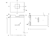
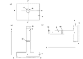
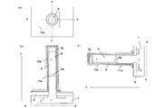
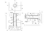
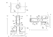
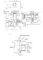
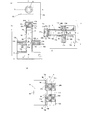
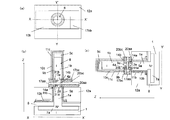
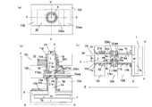
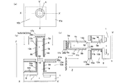
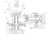
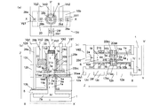
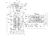
- They are a top view (a) for explaining a manufacturing method of a columnar semiconductor device which has SGT concerning a 1st embodiment, a sectional structure figure (b), (c), and an enlarged sectional view (d). They are a top view (a) for explaining a manufacturing method of a columnar semiconductor device which has SGT concerning a 1st embodiment, a sectional structure figure (b), (c), and an enlarged sectional view (d). It is the top view (a) and sectional structure drawing (b), (c) for demonstrating the manufacturing method of the columnar semiconductor device which has SGT which concerns on 1st Embodiment.
- FIG. 1A shows a plan view and a cross-sectional view for explaining a first step of a columnar semiconductor device having an SGT.
- (A) is a plan view
- (b) is a cross-sectional structure diagram taken along line X-X 'in (a)
- (c) is a cross-sectional structure diagram along line Y-Y' in (a).
- the other drawings referred to below also have the same relationship between the drawings shown in (a), (b), and (c).
- an SiO 2 layer (not shown) is formed on the i-layer substrate 1 by a thermal oxidation method. Then, the SiO 2 layer 5a provided with holes for injecting oxygen ions (O + ) is formed by lithography and RIE (Reactive Ion Etching). The hole may be rectangular or circular in plan view. Next, oxygen ions are ion-implanted from the upper surface of the i-layer substrate 1 at an acceleration voltage of 100 to 200 KV and a dose of 2 ⁇ 10 18 / cm 2 , for example. Then, for example, heat treatment at 1150 ° C. is performed to form the SiO 2 region 4 in the i-layer substrate 1 (see, for example, Non-Patent Document 2 for the formation of the SiO 2 region 4).
- an SiO 2 layer 5b is deposited on the exposed i-layer substrate 1 and the SiO 2 layer 5a.
- the SiO 2 layer 5c is formed by etching the SiO 2 layer 5b using a lithography method and an RIE method. Further, by etching the i-layer substrate 1 by the RIE method using the SiO 2 layer 5c as a mask, a Si pillar having a SiO 2 layer 4a extending in the vertical (up and down) direction with respect to the surface of the i-layer substrate 1 and having the SiO 2 layer 4a at the center. 6 is formed.
- the cross-sectional shape of the Si pillar 6 is preferably a circle smaller than the hole of the SiO 2 layer 5a, as shown in FIG. 1C (a).
- the angle of the side surface of the Si pillar 6 is preferably substantially perpendicular to the upper surface of the i-layer substrate 1.
- an N + region 7 is formed on the upper surface layer of the i-layer substrate 1 on the outer periphery of the Si pillar 6 by ion implantation.
- an SiO 2 film (not shown) is deposited using a CVD (Chemical Vapor Deposition) method, and the upper surface of the SiO 2 film is planarized using an MCP (Mechanical Chemical Polishing) method, followed by an etch back method. Is used to etch the SiO 2 film.
- the SiO 2 layer 8 remains on the i-layer substrate 1 and the N + region 7 on the outer periphery of the Si pillar 6.
- the entire Si pillar 6 and the SiO 2 layer 8 are sequentially covered with a hafnium oxide (HfO 2 ) layer 9 and a titanium nitride (TiN) layer 10 by an ALD (Atomic Layer Deposition) method.
- HfO 2 hafnium oxide
- TiN titanium nitride
- ALD Atomic Layer Deposition
- the Si pillar 6 and the entire periphery of the Si pillar 6 are covered with the SiO 2 layer 11 by the CVD method.
- the HfO 2 layer 9 becomes an SGT gate insulating layer
- the TiN layer 10 becomes an SGT gate conductor layer.
- the SiO 2 layer 11 and the TiN layer 10 are etched by the RIE method, so that the SiO 2 layer 8 is formed from the upper surface of the Si pillar 6.
- An SiO 2 layer 11a and a TiN layer 10a are formed over the upper surface.
- a silicon nitride (SiN) layer 12 a is formed on the outer periphery of the Si pillar 6.
- a resist layer 13 is formed on the SiN layer 12a.
- the resist layer 13 is formed so that the position of the SiO 2 layer 4a in the vertical direction is the center of the resist layer 13.
- the resist layer 13 is formed by applying a resist material to the entire upper surface of the i-layer substrate 1 and then performing a heat treatment at, for example, 200 ° C. to increase the fluidity of the resist material. It forms so that it may accumulate uniformly above.
- hydrogen fluoride gas hereinafter referred to as “HF gas” is supplied to the whole.
- the HF gas is ionized by moisture contained in the resist layer 13, and hydrogen fluoride ions (HF 2 + ) (hereinafter referred to as “HF ions”).
- HF ions hydrogen fluoride ions
- This HF ion diffuses in the resist layer 13 and etches the SiO 2 layer 11a in contact with the resist layer 13 (see Non-Patent Document 3 for the etching mechanism here).
- the SiO 2 layer 11a not in contact with the resist layer 13 remains almost unetched. Thereafter, the resist layer 13 is removed.
- the SiO 2 layer 11a is separated into the SiO 2 layer 11b in the region covered with the SiN layer 12a and the SiO 2 layer 11c in the upper region of the Si pillar 6. Subsequently, by using the SiO 2 layers 11b and 11c as a mask, the TiN layer 10a is etched, so that the TiN layer 10a is separated from the TiN layer 10b covered with the SiO 2 layer 11b in the lower region of the Si pillar 6, and the Si pillar 6 is separated into a TiN layer 10c covered with the SiO 2 layer 11c.
- the HfO 2 layer 9 is etched, so that the HfO 2 layer 9 is separated from the Si pillar 6 by the TiN layer 10b.
- the HfO 2 layer 9a partially covered and the HfO 2 layer 9b covered with the TiN layer 10c in the upper region of the Si pillar 6 are separated.
- an opening 30a is formed on the side surface of the Si pillar 6.
- the exposed portions of the TiN layers 10b and 10c are oxidized to form TiO (titanium oxide) layers 14a and 14b.
- N + region 7 a As atoms in the N + region 7 are diffused into the i-layer substrate by heat treatment to form the N + region 7 a. Then, for example, a substrate metal plate on which the i-layer substrate 1 is arranged and a counter metal plate spaced from the substrate metal plate are prepared, a DC voltage is applied to the substrate metal plate, and RF is applied to these two parallel metal plates. Ni atoms are incident on the upper surface of the i-layer substrate 1 from a direction perpendicular to each other by using a bias sputtering method in which the material atoms of the opposing metal plate are sputtered and deposited on the i-layer substrate 1 by applying a high-frequency voltage.
- the Ni layer 15a is formed on the SiN layer 12a, and the Ni layer 15c is formed on the Si pillar 6.
- a poly-Si layer 16a containing arsenic (As) impurities is formed on the Ni layer 15a by bias sputtering, and a poly-Si layer 16c containing arsenic (As) atoms serving as donor impurities on the Ni layer 15c.
- SiO 2 atoms are incident from a direction perpendicular to the upper surface of the i-layer substrate 1 to form an SiO 2 layer 17a on the poly Si layer 16a, and on the poly Si layer 16c.
- a SiO 2 layer 17c is formed.
- the Ni layer 15a, the poly Si layer 16a, and the SiO 2 layer 17a by using the same method as the Ni layer 15a, the poly Si layer 16a, and the SiO 2 layer 17a, the Ni layer 15b and the poly Si layer 16b containing boron (B) atoms serving as acceptor impurities on the SiO 2 layer 17a, The SiO 2 layer 17b is formed, and the Ni layer 15d, the poly Si layer 16d containing boron (B) atoms, and the SiO 2 layer 17d are formed on the SiO 2 layer 17c.
- Ni atoms, poly Si atoms, and SiO 2 atoms are incident from a direction perpendicular to the upper surface of the i-layer substrate 1, the side surfaces of the Si pillar 6 outer periphery, the Ni layers 15a and 15b, the poly Si layers 16a and 16b, A space 18 is formed between the SiO 2 layer 17a.
- FIG. 1H (d) shows an enlarged view in the dotted line frame A of FIG. 1H (b).
- the upper surface position of the SiO 2 layer 17 b is formed to be above the upper end position of the space 18. Since the SiO 2 layer 17b is in contact with the SiO 2 layer 11c, a sealed space 18 is formed.
- NiSi layers 15a and 15b are diffused into the poly-Si layers 16a and 16b, thereby forming nickel silicide (NiSi) layers 20a and 20b.
- the NiSi layers 20a and 20b expand from the volume of the poly-Si layers 16a and 16b (refer to Non-Patent Document 4 for the volume expansion). Since the poly Si layer 16a is sandwiched between the SiN layer 12a and the SiO 2 layer 17a, and the poly Si layer 16b is sandwiched between the SiO 2 layers 17a and 17b, the NiSi layers 20a and 20b mainly project into the space 18. .
- Non-Patent Document 4 for the sweep-out phenomenon.
- projections 21a and 21b containing a large amount of impurity atoms are formed on the side surface layers of the NiSi layers 20a and 20b protruding into the space 18.
- the side surfaces of the protrusions 21a and 21b are in contact with the surface of the Si pillar 6. Thereafter, the NiSi layers 20c and 20d, the protrusions 21c and 21d, and the SiO 2 layers 17c and 17d on the Si pillar 6 are removed.
- FIG. 1I (d) shows an enlarged view in the dotted line frame A of FIG. 1I (b).
- the side surfaces of the projection 21a containing a lot of donor impurity As atoms and the projection 21b containing a lot of acceptor impurity B atoms are in contact with the side surface of the Si pillar 6.
- the upper surface position of the SiO 2 layer 17 b is formed to be above the upper end position of the space 18.
- the thermal diffusion of donor and acceptor impurity atoms is suppressed, and at the same time silicidation is also suppressed, so that the N + region 2a and the P + region 3a are separated by the SiO 2 layer 4a.
- the NiSi layers 20a and 20b and the SiO 2 layers 17a and 17b using the lithography method and the RIE method, the NiSi layers 20aa and 20bb, the SiO 2 layer 17aa, 17bb is formed.
- NiSi layer 20b and the SiO 2 layer 17b using a lithography method and an RIE method, the NiSi layer 20aa and the SiO 2 layer 17aa in the XX ′ axis direction. Then, a NiSi layer 20bc and a SiO 2 layer 17bc which are further receded to the Si pillar 6 side are formed.
- the SiN layer 12b is formed so that its upper surface is located in the middle of the TiN layer 10c in the height direction.
- the opening 30b is formed on the outer periphery of the TiN layer 10c by using the same method as the method of forming the opening 30a.
- a NiSi layer 22 in contact with the TiN layer 10c is formed.
- the SiO 2 layer 12 c is formed such that the position of the upper surface is higher than the surface of the NiSi layer 22 and lower than the top of the Si pillar 6.
- the SiO 2 layer 11c, the TiN layer 10c, and the HfO 2 layer 9b are etched to form the SiO 2 layer 11d, the TiN layer 10d, and the HfO 2 layer 9c.
- a boron (B) ion implantation method is used to form a P + region 24 on the top of the Si pillar 6.
- the SiO 2 layer 12d is formed entirely by the CVD method and the MCP method. Subsequently, using the lithography method and the RIE method, the SiO 2 layers 12d and 12c and the SiN layers 12b and 12a are penetrated to form the contact hole 28a on the TiN layer 10b, and the SiO 2 layers 12d and 12c are penetrated.
- a contact hole 28b on the NiSi layer 22 Te by penetrating the SiO 2 layer 12d to form a contact hole 28c on top of the Si pillar 6, the SiO 2 layer 12d, 12c, SiN layer 12b, the SiO 2 layer 17bc It was allowed to penetrate to form the contact holes 28d on the NiSi layer 20bc, SiO 2 layer 12d, 12c, SiN layer 12b, to form a contact hole 28e on the NiSi layer 20aa by penetrating the SiO 2 layer 17aa, SiO 2 layer 12d, 12c, SiN layers 12b, 12a, HfO 2 layer 9a, and SiO 2 layer 8 are penetrated.
- Contact hole 28f is formed on N + region 7a.
- a gate wiring metal layer Vg1 electrically connected to the TiN layer 10b through the contact hole 28a is formed, and a gate wiring metal layer Vg2 electrically connected to the NiSi layer 22 through the contact hole 28b is formed.
- a drain wiring metal layer Vd2 electrically connected to the P + region 24 at the top of the Si pillar 6 through the contact hole 28c is formed, and a source wiring metal electrically connected to the NiSi layer 20bc through the contact hole 28d.
- a layer Vs2 is formed, a drain wiring metal layer Vd1 electrically connected to the NiSi layer 20aa via the contact hole 28e is formed, and a source wiring metal layer electrically connected to the N + region 7a via the contact hole 28f Vs1 is formed.
- NiSi layers 20aa and 20bc are separated by the space 18 and the SiO 2 layer 17aa. Moreover, it is preferable that a space remains between the NiSi layers 20aa and 20bc and the TiO layers 14a and 14b. This improves the electrical insulation between the TiN layers 10b and 10d, which are gate conductor layers, and the NiSi layers 20aa and 20bc.
- the i layer 1a below the Si pillar 6 is the channel
- the HfO 2 layer 9a surrounding the outer periphery of the i layer 1a is the gate insulating layer
- the TiN layer 10b surrounding the outer periphery of the HfO 2 layer 9a is the gate conductor layer
- An N channel type SGT that functions as an N + region 7a positioned below the i layer 1a as a source and an N + region 2a positioned above the i layer 1a as a drain
- an i layer 1b above the Si pillar 6 as a channel
- the HfO 2 layer 9c surrounding the outer periphery of the i layer 1b is the gate insulating layer
- the TiN layer 10d surrounding the outer periphery of the HfO 2 layer 9c is the gate conductor layer
- the P + region 3a located below the i layer 1b is the source
- the i layer 1b P channel type SGTs are formed, each of which functions as a drain of the P + region
- the N channel type SGT and the P channel type SGT are separated by the SiO 2 layer 4a.
- the drain N + region 2a of the N-channel SGT below the Si pillar 6 and the source P + region 3a of the P-channel SGT above are electrically independent of the drain wiring metal layer Vd1.
- the source wiring metal layer Vs2 is taken out.
- the N channel SGT is formed at the lower part of the Si pillar 6 and the P channel SGT is formed at the upper part.
- the donor or acceptor impurity included in the poly Si layers 16a and 16b in FIG. 1H is selected. By doing so, the channel type of the upper and lower SGTs can be changed to either the N channel or the P channel.
- the expansion of the NiSi layers 20a and 20b into the space 18 and the connection of the protrusions 21a and 21b containing a large amount of donor or acceptor impurity atoms to the side surfaces of the Si pillar 6 were performed. , It may be performed in subsequent steps. Up to the final step, the structure shown in FIG. 1N may be obtained.
- the NiSi layers 31a, 31b, the N + region 2a, and the P + region 3a are formed by a single heat treatment.
- the NiSi layers 31a, 31b, and the N + region are not formed by forming the + region 2a and the P + region 3a but before the final step of manufacturing the SGT by a plurality of heat treatments in the steps illustrated in FIGS. 1I to 1L.
- the formation of the 2a and P + regions 3a may be performed.
- the columnar semiconductor device manufacturing method has the following effects.
- two electrically independent SGTs separated by the SiO 2 layer 4a and the SiO 2 layer 17aa are formed above and below the Si pillar 6.
- the channel types of the upper and lower SGTs can be independently N-channel type or P-channel type depending on circuit design. Thereby, a high-density SGT circuit can be realized.
- the N + region 2a is formed using the NiSi layer 20a whose lower end position is at the upper end position of the TiN layer 10b serving as the gate of the lower SGT as a diffusion source of donor impurity As atoms.
- the drain N + region 2a and the gate TiN layer 10b are formed by self-alignment.
- the P + region 3a is formed using the NiSi layer 20b whose upper surface position is the lower end position of the TiN layer 10c serving as the gate of the upper SGT as a diffusion source of acceptor impurity B atoms.
- the drain P + region 3a and the gate TiN layer 10c are formed by self-alignment.
- the self-alignment formation of the N + regions 2a and P + regions 3a of the two drains and the gate TiN layers 10b and 10c is performed at the same time.
- the drain N + region 2a and the P + region 3a are not formed separately, but are formed simultaneously. This leads to cost reduction of manufacturing an IC (Integrated Circuit) on which the SGT circuit is mounted. In addition, this has an advantage that a circuit with less performance variation can be formed because the positional relationship between the drain N + region 2a and the P + region 3a can be accurately formed. 4).
- NiSi is an impurity diffusion source of P + region 3a forming layer 20a, 20b is, the drain N + region 2a, a lead wiring material layer of P + region 3a. This leads to a reduction in cost of manufacturing an IC on which SGT is mounted. 5.
- the NiSi layers 20a, 20b, 20aa, and 20bb remain from the process of forming the NiSi layers 31a and 31b in the Si pillar 6 and in the subsequent processes.
- the NiSi layers 20a, 20b, 20aa, and 20bb have a structure that supports the Si pillar 6, and play a role of preventing the Si pillar 6 from falling or bending. 6). In FIG.
- a space remains between the NiSi layers 20aa and 20bc and the TiO layers 14a and 14b, thereby improving the electrical insulation between the TiN layers 10b and 10d, which are gate conductor layers, and the NiSi layers 20aa and 20bc. To do.
- material atoms are made incident on the surface of the i-layer substrate 1 from the vertical direction by sputtering, so that the SiN layer 12a is exposed. Then, the Ni layer 15a, the poly Si layer 29a not containing impurity atoms, and the SiO 2 layer 17a are deposited. Thereafter, As atoms are implanted into the poly-Si layer 29a by ion implantation.
- material atoms are made incident on the surface of the i-layer substrate 1 from the vertical direction by sputtering to form a Ni layer 15b on the SiO 2 layer 17a and a polycrystal containing no impurity atoms.
- the Si layer 29b and the SiO 2 layer 17b are deposited.
- B atoms are implanted into the poly-Si layer 29b by ion implantation.
- a poly Si layer 29a containing donor impurity As atoms and a poly Si layer 29b containing acceptor impurity B atoms are formed.
- donor and acceptor impurity atoms are introduced into the poly-Si layers 29a and 29b by an ion implantation method.
- a circuit is formed by lithography and ion implantation.
- N-channel or P-channel SGTs can be easily formed above and below a plurality of Si pillars.
- FIGS. 3A and 3B a method for manufacturing a columnar semiconductor device having SGTs according to a third embodiment of the present invention will be described with reference to FIGS. 3A and 3B.
- the columnar semiconductor device of the third embodiment is manufactured by a process similar to the process shown in FIGS. 1A to 1N of the first embodiment except that the structural differences described below occur.
- material atoms are made incident from a direction perpendicular to the upper surface of the i-layer substrate 1 by using a bias sputtering method, and NiN is formed on the SiN layer 12a.
- the layer 15a, the N-type poly-Si layer 29aa containing arsenic (As) impurities, the SiO 2 layer 17a, the Ni layer 15b, the N-type poly-Si layer 29bb containing arsenic (As) impurities, and the SiO 2 layer 17b are formed.
- acceptor impurity B atoms are implanted into the poly-Si layer 29bb at a concentration higher than the donor impurity concentration previously contained in the poly-Si layer 29bb by ion implantation. Thereby, a P-type poly-Si layer 29bb is formed. Thereafter, the steps of FIGS. 1I to 1N are performed.
- the poly Si layer 29aa is converted into a P-type.
- the poly Si layer 29bb can be made N-type.
- both layers 29aa and 29bb can be P-type.
- both the poly Si layers 29aa and 29bb can be made N-type.
- N-channel or P-channel SGTs can be easily formed above and below the plurality of Si pillars according to circuit design by lithography and ion implantation.
- the ion implantation process can be reduced by half compared to the second embodiment.
- the Si 1-x Ge x layer 33 becomes a drain layer of the P channel type SGT corresponding to the P + region 24 in FIG. 1L.
- the Si 1-x Ge x layer 33 generates stress from the Si 1-x Ge x layer 33 toward the lower side of the Si column 6 due to the difference in the interstitial distance of the Si atoms of the Si column 6.
- the P + region 3a in the middle of the Si pillar 6 receives compressive stress from the NiSi layers 20aa and 20bb protruding and connected to the outer periphery of the Si pillar 6. This compressive stress has a stress component directed upward from the P + region 3a to the Si pillar 6.
- the channel i layer 1b of the P-channel type SGT of the Si pillar 6 sandwiched between the Si 1-x Ge x layer 33 and the P + region 3a is the Si 1-x Ge x layer 33.
- silicided NiSi layers 31 c and 31 d are formed from the side surfaces of the NiSi layers 20 aa and 20 bb to the center of the cross section in the N + regions 2 a and the P + regions 3 a in the Si pillar 6.
- the NiSi layers 31c and 31d are separated by the SiO 2 layer 4a.
- the NiSi layers 31a and 31b were formed on the side surface layer of the Si pillar 6, but in the fifth embodiment, the NiSi layers 31c and 31d corresponding to the NiSi layers 31a and 31b are cross-sections of the Si pillar 6. Silicided to the center and formed. According to the fifth embodiment, the Si pillar 6 falls or bends due to the formation of NiSi layers 31c and 31d having different expansion coefficients in the entire cross section at the intermediate portion of the Si pillar 6, and the outer periphery of the NiSi layers 31c and 31d. The surrounding NiSi layers 20aa and 20bc can be prevented by remaining without being removed. This is more effective when the cross-sectional diameter of the Si pillar 6 is small.
- the upward stress from the NiSi layer 31d compared to the case where the NiSi layers 31a and 31b shown in FIG. Can be increased.
- the hole mobility is improved, and the current driving capability of the P-channel SGT can be further increased.
- a NiSi layer 31c is formed in the Si pillar 6 connected to the N + region 2a.
- a NiSi layer 20aa is formed so as to be connected to the NiSi layer 31c and surround the Si pillar 6.
- a NiSi layer 31d is formed in the Si pillar 6 connected to the P + region 3a.
- a NiSi layer 20bb is formed so as to surround the Si pillar 6 connected to the NiSi layer 31d.
- the NiSi layer 20aa, the SiO 2 layer 17aa, the NiSi layer 20bb, and the SiO 2 layer 17bb are formed in the same shape in plan view.
- a contact hole 28c is formed on the SiN layer 12a through the SiO 2 layers 12d and 12c, the SiN layer 12b, the NiSi layer 20aa, the SiO 2 layer 17aa, the NiSi layer 20bb, and the SiO 2 layer 17bb (the contact hole 28c).
- the bottom surface may be the top surface or the middle part of the NiSi layer 20aa).
- the NiSi layer 22a connected to the TiN layer 10d is formed in the same shape as the TiN layer 10b.
- a contact hole 28a is formed on the TiN layer 10b through the SiO 2 layers 12d and 12c, the NiSi layer 22a, and the SiN layers 12b and 12a.
- the input wiring metal layer Vin is formed through the contact hole 28a
- the power supply wiring metal layer Vdd is formed through the contact hole 28b
- the output wiring metal layer Vout is formed through the contact hole 28c
- the contact hole 28d is formed through the contact hole 28d.
- a ground wiring metal layer Vss is formed via
- the NiSi layers 20aa and 20bb are electrically connected via the output wiring metal layer Vout.
- the NiSi layer 22a and the TiN layer 10b are electrically connected via the input wiring metal layer Vin.
- a CMOS inverter circuit having an N channel type SGT in the lower part and a P channel type SGT in the upper part is formed in the Si pillar 6.
- material atoms are incident from a direction perpendicular to the upper surface of the i-layer substrate 1 by using a bias sputtering method, whereby Ni layers 15a and 15b, poly Si layers 16a and 16b, SiO Two layers 17a and 17b were formed.
- a bias sputtering method Any method other than the bias sputtering method may be used as long as the material atoms can be incident from a direction perpendicular to the upper surface of the i-layer substrate 1. This is similarly applicable to other embodiments according to the present invention.
- the NiSi layers 20a and 20b are projected into the space 18 along with the silicidation of the poly-Si layers 16a and 16b.
- another metal layer such as titanium (Ti) or cobalt (Co) may be used to project the silicide layer into the space 18. This is similarly applicable to other embodiments according to the present invention.
- the Ni layers 15a and 15b are formed in the lower layer, and the poly Si layers 16a and 16b containing donor or acceptor impurities are formed in the upper layer.
- the Ni layers 15a and 15b are formed in the upper layer, Poly Si layers 16a and 16b containing donor or acceptor impurities may be formed in the lower layer. This is similarly applicable to other embodiments according to the present invention.
- the NiSi layers 20a and 20b are formed by the subsequent heat treatment from the two layers of the Ni layer 15a and the poly-Si layer 16a and the two layers of the Ni layer 15b and the poly-Si layer 16b.
- the layers 15a and 15b may be formed either above or below the poly-Si layers 16a and 16b.
- the NiSi layers 20a and 20b may be formed from a plurality of Ni layers and a plurality of poly-Si layers, respectively. This is similarly applicable to other embodiments according to the present invention.
- the Si pillar 6 having a side surface angle of approximately right angle (about 90 degrees) with respect to the upper surface of the i-layer substrate 1 is formed, and the material atoms are i-layered by bias sputtering.
- Ni layers 15a and 15b, poly Si layers 16a and 16b, and SiO 2 layers 17a and 17b were formed by incidence from a direction perpendicular to the upper surface of the substrate 1.
- the side surface angle of the Si pillar 6 may be smaller than 90 degrees as long as Ni, Si, and SiO 2 material atoms are not deposited on the side surface of the SiO 2 layer 11c surrounding the outer periphery of the Si pillar 6.
- the bias voltage applied between the substrate electrode plate on which the i-layer substrate 1 is disposed and the counter electrode plate spaced from the i-layer substrate 1 is controlled, so that the SiO 2 layer 11c side It is possible to prevent Ni, Si, and SiO 2 material atoms from being deposited on the surface of the part (refer to Non-Patent Document 6 for the basic method for this).
- the side surface of the Si pillar 6 and the NiSi layers 20a and 20b are connected, the NiSi layers 31a and 31b are formed in the Si pillar 6, and the N + region 2a and the P + region 3a are formed.
- the heat treatment in FIG. 1J was performed.
- the connection between the side surface of the Si pillar 6 and the NiSi layers 20a and 20b, the formation of the NiSi layers 31a and 31b in the Si pillar 6, and the formation of the N + region 2a and the P + region 3a are performed until the final step of manufacturing the SGT. It only has to be done. This is also applicable to other embodiments according to the present invention.
- the poly Si layers 20a and 20b are used, but an amorphous layer may be used. This is also applicable to other embodiments according to the present invention.
- the single material layer of the SiN layers 12a and 12b has been described.
- an SiO 2 layer may be used for the lower portion and an SiN layer may be used for the upper portion.
- the SiN layers 12a and 12b may be used instead.
- An insulating material layer having a small diffusion coefficient of HF ions may be used. This is also applicable to other embodiments according to the present invention.
- the NiSi layers 31c and 31d are formed by silicidation up to the center of the cross section of the Si pillar 6. This is applicable to the other embodiments because there is no problem in the SGT operation in the other embodiments according to the present invention.
- the present invention is not limited to this, and the technical idea of the present invention can also be applied to a semiconductor device having an SGT using a semiconductor pillar made of a semiconductor material other than silicon.
- each of the above embodiments has been described using a method for manufacturing a semiconductor device in which two SGTs are formed on one Si pillar.
- the present invention is not limited to this, and the technical idea of the present invention can also be applied to a method of manufacturing a semiconductor device having one semiconductor pillar or three or more SGTs.
- the N channel type SGT is formed in the lower portion and the P channel type SGT is formed in the upper portion.
- the P channel type SGT is formed in the lower portion, and the N channel type SGT is formed in the upper portion.
- the technical idea of the present invention can also be applied to a circuit in which is formed. Further, the technical idea of the present invention can be applied to the formation of a circuit using N-channel or P-channel SGT both in the upper and lower sides. This is also applicable to other embodiments according to the present invention.
- the SGT has the HfO 2 layer (gate insulating layer) 9c formed on the outer periphery of the semiconductor column such as the Si column 6, and the TiN layer (gate conductor layer) 10d formed on the outer periphery of the HfO 2 layer 9c. It has a formed structure.
- the present invention is not limited to this, and a non-volatile memory element having a conductive layer electrically floating between the gate insulating layer and the gate conductive layer or a charge storage layer such as a SiN layer is also a kind of SGT.
- the technical idea of the present invention can also be applied to such a nonvolatile memory element. In this case, it is preferable to use a SiO 2 layer as a tunnel oxide film instead of the HfO 2 layer.
- the gate insulating layer is formed of an HfO 2 layer.
- the present invention is not limited to this, and the gate insulating layer may be formed of another insulating material.
- the gate conductive layer is composed of the TiN layers 10b and 10d.
- the present invention is not limited to this, and the gate conductive layer may be formed of another metal material.
- the gate conductive layer may have a multilayer structure including a metal layer and, for example, a poly-Si layer.
- the impurity region composed of the N + region 2a and the P + region 3a may be composed of impurity layers having different conductivity types as described above, or may be composed of impurity layers having the same conductivity type.
- the impurity regions are of the same conductivity type, the two impurity layers constitute one impurity region having the same type of conductivity as a whole.
- the impurity regions are of different conductivity types, similarly, the two impurity layers constitute one impurity region as a whole.
- Such a configuration can be similarly applied to other embodiments according to the present invention.
- the exposed portions of the TiN layers 10b and 10c are oxidized to form the insulating TiO layers 14a and 14b. Since the insulating TiO layers 14a and 14b are obtained by oxidizing the TiN layers 10b and 10c, they contain N atoms. Therefore, the insulating TiO layers 14a and 14b may be insulating layers containing Ti atoms. This is also applicable to other embodiments according to the present invention.
- the insulating TiO layers 14a and 14b may not be provided. This is also applicable to other embodiments according to the present invention.
- the exposed portions of the TiN layers 10b and 10c are oxidized to form the insulating TiO layers 14a and 14b.
- another insulating layer such as a SiO 2 layer may be covered.
- the entire Si pillar 6 is covered by the ALD method to cover the SiO 2 film, and then the opening 30a shown in FIG. 1E is used to form the TiN layers 10b and 10c.
- the opening may be formed with the exposed portion covered with the SiO 2 layer.
- an SOI (Silicon on Insulator) substrate may be used instead of the i-layer substrate 1, and the SiO 2 layer of the SOI substrate may be used as the SiO 2 region 4 in FIG. 1B.
- the same SiO 2 layer and the SiO 2 layer 4a is formed to other Si pillar formed on the i-layer substrate 1. This is also applicable to other embodiments according to the present invention.
- the SiO 2 layer 5b is, for example SiN It may be another insulating layer such as a layer. This applies to other embodiments of the invention as well.
- the Si 1-x Ge x layer 33 that generates stress below the Si column 6 is used at the top of the Si column 6, but stress is generated below the Si column 6 and P Another material layer may be used as long as it is a material layer that becomes a source or drain of the channel type SGT.
- one or two of the two SGTs formed above and below the Si pillar 6 have a source current and a drain current generated by a voltage applied to the gate conductor layer, and the N + region 2a. , 7a and P + regions 3a, 24 may be used. This applies to other embodiments of the invention as well.
- the present invention is capable of various embodiments and modifications without departing from the broad spirit and scope of the present invention. Further, the above-described embodiment is for explaining an example of the present invention, and does not limit the scope of the present invention. The said Example and modification can be combined arbitrarily. Furthermore, even if a part of the structural requirements of the above-described embodiment is removed as necessary, it is within the scope of the technical idea of the present invention.
- the columnar semiconductor device manufacturing method according to the present invention provides a highly integrated semiconductor device.
Landscapes
- Insulated Gate Type Field-Effect Transistor (AREA)
- Metal-Oxide And Bipolar Metal-Oxide Semiconductor Integrated Circuits (AREA)
- Electrodes Of Semiconductors (AREA)
- Thin Film Transistor (AREA)
Abstract
Si柱(6)の中間位置にSiO2層(4a)を形成する。SiO2層(4a)側面を含む外周部にゲート絶縁層、ゲート導体層の開口部を形成する。この開口部の外周部にNi層、ドナーまたはアクセプタ不純物原子を含んだポリSi層、SiO2層を各2つ重ねた積層層を形成し、熱処理を行い、ポリSi層のシリサイド化を行う。このシリサイド化により突き出てSi柱(6)側面に接触したNiSi層からドナーまたはアクセプタ不純物原子をSi柱(6)内へ拡散させることによりSGTのソースまたはドレインとなるN+領域(2a)、P+領域(3a)を、SiO2層(4a)の上下に形成する。
Description
本発明は、柱状半導体装置と、その製造方法に関する。
近年、代表的な柱状半導体装置であるSGT(Surrounding Gate MOS Transistor)は、高集積な半導体装置を提供する半導体素子として注目されている。また、SGTを有する半導体装置の更なる高集積化が求められている。
通常のプレナー型MOSトランジスタでは、チャネルが半導体基板の上表面に沿う水平方向に存在する。これに対して、SGTのチャネルは、半導体基板の上表面に対して垂直な方向に存在する(例えば、特許文献1、非特許文献1を参照)。このため、SGTはプレナー型MOSトランジスタと比べ、半導体装置の高密度化が可能である。
図7に、NチャネルSGTの構造模式図を示す。P型又はi型(真性型)の導電型を有するSi柱100(以下、シリコン半導体柱を「Si柱」と称する。)の上下の位置に、一方がソースとなる場合に、他方がドレインとなるN+領域101a、101b(以下、ドナー不純物を高濃度で含む半導体領域を「N+領域」と称する。)が形成されている。このソース、ドレインとなるN+領域101a、101b間のSi柱100がチャネル領域102となる。このチャネル領域102を囲むようにゲート絶縁層103が形成され、このゲート絶縁層103を囲むようにゲート導体層104が形成されている。SGTでは、ソース、ドレインとなるN+領域101a、101b、チャネル領域102、ゲート絶縁層103、ゲート導体層104が、単一のSi柱100内に形成される。このため、SGTの平面視での面積は、プレナー型MOSトランジスタの単一のソース又はドレインN+領域面積に相当する。そのため、SGTを有する回路チップは、プレナー型MOSトランジスタを有する回路チップと比較して、更なるチップサイズの縮小化が実現できる。
例えば、図8の構造模式図に示すように、1つのSi柱115の上下の位置に2つのSGT116a、116bを形成することにより、回路面積が縮小できることが予測される。
図8に、Si柱115の下方にNチャネルSGT116aが形成され、このNチャネルSGT116aの上方にPチャネルSGT116bが形成された回路の模式構造図を示す。P層基板117(以下、アクセプタ不純物を含む半導体層を「P層」と称する。)上にSi柱115が形成されている。Si柱115の外周かつP層基板117上にSiO2層118が形成されている。また、Si柱115を囲むように、NチャネルSGT116aのゲート絶縁層119aと、PチャネルSGT116bのゲート絶縁層119bが形成されている。ゲート絶縁層119a、119bを囲むように、Si柱115の外周に、NチャネルSGT116aのゲート導体層120aと、PチャネルSGT116bのゲート導体層120bが形成されている。Si柱115の底部に繋がるP層基板117の表層部にN+領域121aが形成されている。Si柱115の中間部に、N+領域121bと、N+領域121b上に繋がったSiO2層130と、SiO2層130上に繋がったP+領域122a(以下、アクセプタ不純物を高濃度で含む半導体領域を「P+領域」と称する。)とが形成されている。Si柱115の頂部にはP+領域122bが形成されている。N+領域121aは、NチャネルSGT116aのソースであり、N+領域121bは、NチャネルSGT116aのドレインである。N+領域121a、121bの間にあるSi柱115は、NチャネルSGT116aのチャネル領域123aである。P+領域122bは、PチャネルSGT116bのドレインであり、P+領域122aは、PチャネルSGT116bのソースである。P+領域122a、122bの間のSi柱115は、PチャネルSGT116bのチャネル領域123bである。Si柱115の底部に繋がるN+領域121aの表層部にニッケルシリサイド層(NiSi層)125aが形成されている。また、Si柱115の中央部にあるN+領域121bの外周にNiSi層125b、P+領域122aの外周にNiSi層125cが形成され、Si柱115の頂部にあるP+領域122bの上部表層にNiSi層125dが形成されている。N+領域121a内のNiSi層125aに繋がるようにソース配線金属層126aが形成され、ソース配線金属層126aはVS1端子に接続されている。NiSi層125bに繋がるようにドレイン配線金属層126bが形成され、ドレイン配線金属層126bはドレイン端子VD1に接続されている。P+領域122a内のNiSi層125cに繋がるようにソース配線金属層126cが形成され、ソース配線金属層126cはVS2端子に接続されている。NiSi層125dに繋がるようにドレイン配線金属層126dが形成され、ドレイン配線金属層126dはVD2端子に接続されている。ゲート導体層120a、120bに繋がるようにゲート配線金属層127a、127bが形成され、ゲート配線金属層127a、127bはそれぞれゲート端子VG1、VG2に接続されている。これにより、Si柱115にSiO2層130により分離された2つのSGT116a、116bが形成される。
図8に示したように、Si柱115にSiO2層130により分離された2つのSGT116a、116bを形成する場合、以下の問題点があった。
1.Si柱115の中間部に、SiO2層130により分離されたN+領域121bと、P+領域122aとを、精度よく、且つ容易に形成することが難しい。
2.N+領域121bと、P+領域122aとの外周部に、NiSi層125b、125cを、精度よく、且つ容易に形成することが難しい。
3.NiSi層125bとドレイン配線金属層126bの接続、NiSi層125cとソース配線金属層126cの接続を、精度よく、且つ容易に形成することが難しい。
4.Si柱115内へのNiSi層125b、125cの形成において、NiSiの線熱膨張係数(12×10-6/K)と、Siの線熱膨張係数(2.4×10-6/K)の違いに起因するSi柱115の曲がり又は倒れを防止することが難しい。
1.Si柱115の中間部に、SiO2層130により分離されたN+領域121bと、P+領域122aとを、精度よく、且つ容易に形成することが難しい。
2.N+領域121bと、P+領域122aとの外周部に、NiSi層125b、125cを、精度よく、且つ容易に形成することが難しい。
3.NiSi層125bとドレイン配線金属層126bの接続、NiSi層125cとソース配線金属層126cの接続を、精度よく、且つ容易に形成することが難しい。
4.Si柱115内へのNiSi層125b、125cの形成において、NiSiの線熱膨張係数(12×10-6/K)と、Siの線熱膨張係数(2.4×10-6/K)の違いに起因するSi柱115の曲がり又は倒れを防止することが難しい。
Hiroshi Takato, Kazumasa Sunouchi, Naoko Okabe, Akihiro Nitayama, Katsuhiko Hieda, Fumio Horiguchi, and Fujio Masuoka: IEEE Transaction on Electron Devices, Vol.38, No.3, pp.573-578 (1991)
Hon Wai Lam : "SIMOX SOI for Integrated Circuit Fablication", IEEE Circuit and Devices Magazine, pp.6-11 ( July 1987)
Tadashi Shibata, Susumu Kohyama and Hisakazu Iizuka: "A New Field Isolation Technology for High Density MOS LSI", Japanese Journal of Applied Physics, Vol.18, pp.263-267 (1979)
T.Morimoto, T.Ohguro, H.Sasaki, M.S.Momose, T.Iinuma, I.Kunishima, K.Suguro, I.Katakabe, H.Nakajima, M.Tsuchiaki, M.Ono, Y.Katsumata, and H.Iwai: "Self-Aligned Nickel-Mono-Silicide Technology for High-Speed Deep Submicrometer Logic CMOS ULSI" IEEE Transaction on Electron Devices, Vol.42, No.5, pp.915-922 (1995)
S.E.Thompson, G.Sun, Y.S.Choi, and T.Nishida: "Uniaxial-Process-Induced Strained-Si: Extending the CMOS Roadmap", IEEE Transaction on Electron Devices, Vol.53, No.5, pp.1010-1020 (1995)
C.Y.Ting, V.J.Vivalda, and H.G.Schaefer:"Study of planarized sputter-deposited SiO2"J.Vac.Sci.Technol, 15(3), May/Jun (1978)
以上のとおり、図8に示すSGTを有する柱状半導体装置においては、
1.Si柱115の中間部に、SiO2層130により分離されたN+領域121bと、P+領域122aとを、精度よく、且つ容易に形成し、
2.N+領域121bと、P+領域122aとの外周部に、NiSi層125b、125cを、精度よく、且つ容易に形成し、
3.NiSi層125bとドレイン配線金属層126bの接続、NiSi層125cとソース配線金属層126cの接続を、精度よく、且つ容易に形成し、
4.Si柱115内へのNiSi層125b、125cの形成において、NiSiの線熱膨張係数(12×10-6/K)と、Siの線熱膨張係数(2.4×10-6/K)の違いに起因するSi柱115の曲がり又は倒れを防止することが求められている。
1.Si柱115の中間部に、SiO2層130により分離されたN+領域121bと、P+領域122aとを、精度よく、且つ容易に形成し、
2.N+領域121bと、P+領域122aとの外周部に、NiSi層125b、125cを、精度よく、且つ容易に形成し、
3.NiSi層125bとドレイン配線金属層126bの接続、NiSi層125cとソース配線金属層126cの接続を、精度よく、且つ容易に形成し、
4.Si柱115内へのNiSi層125b、125cの形成において、NiSiの線熱膨張係数(12×10-6/K)と、Siの線熱膨張係数(2.4×10-6/K)の違いに起因するSi柱115の曲がり又は倒れを防止することが求められている。
本発明の第1の観点に係る、柱状半導体装置は、
半導体基板上に、前記半導体基板平面に対して垂直方向に立った半導体柱と、
前記半導体柱内に形成された、第1の層間絶縁層と、
前記半導体柱内に、前記第1の層間絶縁層に接して、且つ前記第1の層間絶縁層の下方に形成された、ドナー又はアクセプタ原子を含む第1の不純物領域と、
前記半導体柱内に、前記第1の層間絶縁層に接して、且つ前記第1の層間絶縁層の上方に形成された、ドナー又はアクセプタ原子を含む第2の不純物領域と、
前記第1の不純物領域の側面に接し、前記半導体柱内と、前記半導体柱の外周とに形成されている第1の合金層と、
前記第2の不純物領域の側面に接し、前記半導体柱内と、前記半導体柱の外周とに形成されている第2の合金層と、
前記第1の合金層と前記第2の合金層との間にあり、且つ側面が前記半導体柱側面と離れて形成された、第2の層間絶縁層とを有する、
ことを特徴とする。
半導体基板上に、前記半導体基板平面に対して垂直方向に立った半導体柱と、
前記半導体柱内に形成された、第1の層間絶縁層と、
前記半導体柱内に、前記第1の層間絶縁層に接して、且つ前記第1の層間絶縁層の下方に形成された、ドナー又はアクセプタ原子を含む第1の不純物領域と、
前記半導体柱内に、前記第1の層間絶縁層に接して、且つ前記第1の層間絶縁層の上方に形成された、ドナー又はアクセプタ原子を含む第2の不純物領域と、
前記第1の不純物領域の側面に接し、前記半導体柱内と、前記半導体柱の外周とに形成されている第1の合金層と、
前記第2の不純物領域の側面に接し、前記半導体柱内と、前記半導体柱の外周とに形成されている第2の合金層と、
前記第1の合金層と前記第2の合金層との間にあり、且つ側面が前記半導体柱側面と離れて形成された、第2の層間絶縁層とを有する、
ことを特徴とする。
前記半導体基板上に、前記半導体基板平面に対して垂直方向に立った前記半導体柱と、
前記半導体柱を囲むゲート絶縁層と、
前記ゲート絶縁層を囲むゲート導体層と、
前記半導体柱の底部に形成された、前記第1の不純物領域と同じ導電性を有する第3の不純物領域と、
前記第2の不純物領域の上方の前記半導体柱内にある、前記第2の不純物領域と同じ導電性を有する第4の不純物領域と、
前記第1の合金層の下面に接した第3の層間絶縁層と、
前記第2の合金層の上面に接した第4の層間絶縁層と、
前記第1の不純物領域と前記第3の不純物領域の一方がソースとして、他方がドレインとして、前記第1の不純物領域と前記第3の不純物領域の間の前記半導体柱の部分がチャネルとして、前記ゲート導体層がゲートとして機能することで第1のSGT(Surrounding Gate MOS Transistor)が形成され、
前記第2の不純物領域と前記第4の不純物領域の一方がソースとして、他方がドレインとして、前記第2の不純物領域と前記第4の不純物領域との間の前記半導体柱の部分がチャネルとして、前記ゲート導体層がゲートとして機能することで第2のSGTとが形成される、
ことが望ましい。
前記半導体柱を囲むゲート絶縁層と、
前記ゲート絶縁層を囲むゲート導体層と、
前記半導体柱の底部に形成された、前記第1の不純物領域と同じ導電性を有する第3の不純物領域と、
前記第2の不純物領域の上方の前記半導体柱内にある、前記第2の不純物領域と同じ導電性を有する第4の不純物領域と、
前記第1の合金層の下面に接した第3の層間絶縁層と、
前記第2の合金層の上面に接した第4の層間絶縁層と、
前記第1の不純物領域と前記第3の不純物領域の一方がソースとして、他方がドレインとして、前記第1の不純物領域と前記第3の不純物領域の間の前記半導体柱の部分がチャネルとして、前記ゲート導体層がゲートとして機能することで第1のSGT(Surrounding Gate MOS Transistor)が形成され、
前記第2の不純物領域と前記第4の不純物領域の一方がソースとして、他方がドレインとして、前記第2の不純物領域と前記第4の不純物領域との間の前記半導体柱の部分がチャネルとして、前記ゲート導体層がゲートとして機能することで第2のSGTとが形成される、
ことが望ましい。
前記第1の合金層と前記第2の合金層は平面視で前記半導体柱の中心まで形成されている、
ことが望ましい。
ことが望ましい。
前記第1の合金層と前記第2の合金層は配線導体材料層である、
ことが望ましい。
ことが望ましい。
前記第1の合金層と前記第2の合金層は、前記第2の合金層と前記第2の層間絶縁層とを貫通し、底部が前記第1の合金層の上面、内部、または下面に達するコンタクトホールを介して、前記コンタクトホールの上部に形成した配線金属層に接続されている、
ことが望ましい。
ことが望ましい。
前記半導体柱にあって、前記第4の不純物領域から下方に向けて応力が形成されている、
ことが望ましい。
ことが望ましい。
前記第1の合金層、及び前記第2の合金層と、前記ゲート導体層との間に、空間を有する、
ことが望ましい。
ことが望ましい。
本発明の第2の観点に係る、柱状半導体装置の製造方法は、
半導体基板上に、前記半導体基板平面に対して垂直方向に立ち、且つ内部に第1の層間絶縁層を有する半導体柱を形成する半導体柱形成工程と、
前記半導体柱の外周部にあり、且つ前記半導体柱側面から離れて、第1の金属層と、ドナー又はアクセプタ原子を含む第1の半導体層と、垂直方向において前記第1の層間絶縁層と同じ高さにある第2の層間絶縁層と、第2の金属層と、ドナー又はアクセプタ原子を含む第2の半導体層と、第3の層間絶縁層とを、前記半導体基板平面に対して垂直方向に積層材料層を積層することで形成する積層材料層形成工程と、
熱処理により、前記第1の金属層と前記第1の半導体層とを反応させた第1の合金層と、前記第2の金属層と前記第2の半導体層とを反応させた第2の合金層とを、形成する第1・第2合金層形成工程と、
熱処理により前記第1の合金層と前記第2の合金層とを、前記半導体柱側面に向けて突出させて、前記第1の合金層と前記第2の合金層とを前記半導体柱の側面に接触させる合金層・半導体柱側面接触工程と、
前記合金層・半導体柱側面接触工程に続き、熱処理により、前記第1の合金層及び前記第2の合金層内の金属原子を前記半導体柱の半導体原子と反応させて前記半導体柱内に前記第1の合金層と前記第2の合金層を広げると共に、前記第1の合金層と、前記第2の合金層から掃き出された前記ドナー又はアクセプタ原子を前記半導体柱内に拡散させて、前記半導体柱内に前記ドナー又はアクセプタ原子を含む、前記第1の合金層に接した第1の不純物領域と、前記第2の合金層に接した第2の不純物領域とを形成する、半導体柱内合金層・不純物領域形成工程と、
を備える、
ことを特徴とする。
半導体基板上に、前記半導体基板平面に対して垂直方向に立ち、且つ内部に第1の層間絶縁層を有する半導体柱を形成する半導体柱形成工程と、
前記半導体柱の外周部にあり、且つ前記半導体柱側面から離れて、第1の金属層と、ドナー又はアクセプタ原子を含む第1の半導体層と、垂直方向において前記第1の層間絶縁層と同じ高さにある第2の層間絶縁層と、第2の金属層と、ドナー又はアクセプタ原子を含む第2の半導体層と、第3の層間絶縁層とを、前記半導体基板平面に対して垂直方向に積層材料層を積層することで形成する積層材料層形成工程と、
熱処理により、前記第1の金属層と前記第1の半導体層とを反応させた第1の合金層と、前記第2の金属層と前記第2の半導体層とを反応させた第2の合金層とを、形成する第1・第2合金層形成工程と、
熱処理により前記第1の合金層と前記第2の合金層とを、前記半導体柱側面に向けて突出させて、前記第1の合金層と前記第2の合金層とを前記半導体柱の側面に接触させる合金層・半導体柱側面接触工程と、
前記合金層・半導体柱側面接触工程に続き、熱処理により、前記第1の合金層及び前記第2の合金層内の金属原子を前記半導体柱の半導体原子と反応させて前記半導体柱内に前記第1の合金層と前記第2の合金層を広げると共に、前記第1の合金層と、前記第2の合金層から掃き出された前記ドナー又はアクセプタ原子を前記半導体柱内に拡散させて、前記半導体柱内に前記ドナー又はアクセプタ原子を含む、前記第1の合金層に接した第1の不純物領域と、前記第2の合金層に接した第2の不純物領域とを形成する、半導体柱内合金層・不純物領域形成工程と、
を備える、
ことを特徴とする。
前記半導体柱形成工程の後に、
前記半導体柱を囲むゲート絶縁層を形成するゲート絶縁層形成工程と、
前記ゲート絶縁層を囲むゲート導体層を形成するゲート導体層形成工程と、
前記ゲート導体層を囲む第4の層間絶縁層を形成する第4層間絶縁層形成工程と、
前記半導体柱の底部にドナー又はアクセプタ原子を含む第3の不純物領域を形成する第3不純物領域形成工程と、
前記半導体柱の外周部にあり、且つ垂直方向における前記第1の層間絶縁層の下面位置より下方に上面を有する第5の層間絶縁層を形成する第5層間絶縁層形成工程と、
前記半導体柱の外周に、前記第5の層間絶縁層の上面位置を下方端として、且つ垂直方向における前記第1の層間絶縁層の上面位置より上方に上方端を有した空孔を、前記第4の層間絶縁層と、前記ゲート導体層と、前記ゲート絶縁層との側面を除去して形成し、前記半導体柱の側面を露出させる半導体柱側面露出工程と、を行い、
前記積層材料層形成工程において、前記第5の層間絶縁層上に、前記第1の金属層と、前記第1の半導体層と、前記第2の層間絶縁層と、前記第2の金属層と、前記第2の半導体層と、前記第3の層間絶縁層との材料原子を、前記半導体基板平面に対して垂直方向から入射させて、前記積層材料層を形成し、
前記積層材料層形成工程の後に、前記合金層・半導体柱側面接触工程と、前記半導体柱内合金層・不純物領域形成工程とを行い、
前記第2の不純物領域の上方の前記半導体柱内に、前記第2の不純物領域と同じ導電性を有する第4の不純物領域を形成する第4不純物領域形成工程をさらに有し、
前記第1の不純物領域と前記第3の不純物領域の一方がソースとして、他方がドレインとして、前記第1の不純物領域と前記第3の不純物領域の間の前記半導体柱の部分がチャネルとして、前記ゲート導体層がゲートとして機能することで第1のSGT(Surrounding Gate MOS Transistor)が形成され、
前記第2の不純物領域と前記第4の不純物領域の一方がソースとして、他方がドレインとして、前記第2の不純物領域と前記第4の不純物領域との間の前記半導体柱の部分がチャネルとして、前記ゲート導体層がゲートとして機能することで第2のSGTとが形成される、
ことが望ましい。
前記半導体柱を囲むゲート絶縁層を形成するゲート絶縁層形成工程と、
前記ゲート絶縁層を囲むゲート導体層を形成するゲート導体層形成工程と、
前記ゲート導体層を囲む第4の層間絶縁層を形成する第4層間絶縁層形成工程と、
前記半導体柱の底部にドナー又はアクセプタ原子を含む第3の不純物領域を形成する第3不純物領域形成工程と、
前記半導体柱の外周部にあり、且つ垂直方向における前記第1の層間絶縁層の下面位置より下方に上面を有する第5の層間絶縁層を形成する第5層間絶縁層形成工程と、
前記半導体柱の外周に、前記第5の層間絶縁層の上面位置を下方端として、且つ垂直方向における前記第1の層間絶縁層の上面位置より上方に上方端を有した空孔を、前記第4の層間絶縁層と、前記ゲート導体層と、前記ゲート絶縁層との側面を除去して形成し、前記半導体柱の側面を露出させる半導体柱側面露出工程と、を行い、
前記積層材料層形成工程において、前記第5の層間絶縁層上に、前記第1の金属層と、前記第1の半導体層と、前記第2の層間絶縁層と、前記第2の金属層と、前記第2の半導体層と、前記第3の層間絶縁層との材料原子を、前記半導体基板平面に対して垂直方向から入射させて、前記積層材料層を形成し、
前記積層材料層形成工程の後に、前記合金層・半導体柱側面接触工程と、前記半導体柱内合金層・不純物領域形成工程とを行い、
前記第2の不純物領域の上方の前記半導体柱内に、前記第2の不純物領域と同じ導電性を有する第4の不純物領域を形成する第4不純物領域形成工程をさらに有し、
前記第1の不純物領域と前記第3の不純物領域の一方がソースとして、他方がドレインとして、前記第1の不純物領域と前記第3の不純物領域の間の前記半導体柱の部分がチャネルとして、前記ゲート導体層がゲートとして機能することで第1のSGT(Surrounding Gate MOS Transistor)が形成され、
前記第2の不純物領域と前記第4の不純物領域の一方がソースとして、他方がドレインとして、前記第2の不純物領域と前記第4の不純物領域との間の前記半導体柱の部分がチャネルとして、前記ゲート導体層がゲートとして機能することで第2のSGTとが形成される、
ことが望ましい。
前記半導体柱内合金層・不純物領域形成工程において、平面視で前記第1の合金層と前記第2の合金層とを前記半導体柱の中心に到達させる、
ことが望ましい。
ことが望ましい。
前記積層材料層形成工程において、
前記第1の金属層と、ドナー及びアクセプタ原子を含まない第3の半導体層とを、形成し、前記第3の半導体層にドナー又はアクセプタ原子をイオン注入して、前記第1の半導体層を形成し、
前記第2の層間絶縁層上に、前記第2の金属層と、ドナー及びアクセプタ原子を含まない第4の半導体層とを、形成し、前記第4の半導体層にドナー又はアクセプタ原子をイオン注入して、前記第2の半導体層を形成する、
ことが望ましい。
前記第1の金属層と、ドナー及びアクセプタ原子を含まない第3の半導体層とを、形成し、前記第3の半導体層にドナー又はアクセプタ原子をイオン注入して、前記第1の半導体層を形成し、
前記第2の層間絶縁層上に、前記第2の金属層と、ドナー及びアクセプタ原子を含まない第4の半導体層とを、形成し、前記第4の半導体層にドナー又はアクセプタ原子をイオン注入して、前記第2の半導体層を形成する、
ことが望ましい。
前記積層材料層形成工程において、
前記第1の金属層と、ドナー及びアクセプタ原子を含む第5の半導体層と、前記第2の層間絶縁層と、前記第2の金属層と、前記第5の半導体層と同じ導電性を有する第6の半導体層とを形成し、前記第5の半導体層と前記第6の半導体層の、いずれか一方、または両方に、前記第5の半導体層と異なる導電性を生じるドナーまたはアクセプタ原子を、前記第5の半導体層に含まれるドナー又はアクセプタ原子よりも多くイオン注入して、前記第1の半導体層と、前記第2の半導体層とを形成する、
ことが望ましい。
前記第1の金属層と、ドナー及びアクセプタ原子を含む第5の半導体層と、前記第2の層間絶縁層と、前記第2の金属層と、前記第5の半導体層と同じ導電性を有する第6の半導体層とを形成し、前記第5の半導体層と前記第6の半導体層の、いずれか一方、または両方に、前記第5の半導体層と異なる導電性を生じるドナーまたはアクセプタ原子を、前記第5の半導体層に含まれるドナー又はアクセプタ原子よりも多くイオン注入して、前記第1の半導体層と、前記第2の半導体層とを形成する、
ことが望ましい。
前記第2の合金層と前記第2の層間絶縁層とを貫通し、底部が前記第1の合金層の上面、内部、または下面に達するコンタクトホールを形成するコンタクトホール形成工程と、
前記コンタクトホールを埋めて、前記第1の合金層と前記第2の合金層とを電気的に接続する配線金属層を形成する配線金属層形成工程と、をさらに有する、
ことが望ましい。
前記コンタクトホールを埋めて、前記第1の合金層と前記第2の合金層とを電気的に接続する配線金属層を形成する配線金属層形成工程と、をさらに有する、
ことが望ましい。
前記半導体柱の下方に向いた応力を発生する前記第4の不純物領域を形成する、
ことが望ましい。
ことが望ましい。
前記第1の合金層、及び前記第2の合金層と、前記ゲート導体層との間に、空間を形成する
ことが望ましい。
ことが望ましい。
本発明によれば、1つの半導体柱の上下に半導体柱の中央部の絶縁層により分離された2つのSGTが形成されているSGTを有する半導体装置において、半導体柱の中央部に形成した絶縁層の上下に形成する、SGTのソースまたはドレインとなる半導体領域が、ゲート導体層の位置に対して、高精度に、且つ容易に形成することが可能となる。また、本発明によれば、半導体柱の中央部に存在する、SGTのソースまたはドレインとなる半導体領域内に合金層を形成する場合に発生する半導体柱の曲がり又は倒れを抑制し、半導体領域と、合金層に繋がる配線金属層との接続を確実にすることが可能となる。
以下、本発明の実施形態に係る、SGTを有する柱状半導体装置の製造方法について、図面を参照しながら説明する。
(第1実施形態)
以下、図1A~図1Nを参照しながら、本発明の第1実施形態に係る、SGTを有する柱状半導体装置の製造方法について説明する。
以下、図1A~図1Nを参照しながら、本発明の第1実施形態に係る、SGTを有する柱状半導体装置の製造方法について説明する。
図1Aに、SGTを有する柱状半導体装置の最初の工程を説明するための、平面図及び断面図を示す。(a)は平面図、(b)は(a)のX-X’線に沿う断面構造図、(c)は(a)のY-Y’線に沿う断面構造図を示す。以下に参照するその他の図面も、(a)、(b)、(c)で示す各図の関係はこれと同様である。
図1Aに示すように、i層基板1上に、熱酸化法によりSiO2層(図示せず)を形成する。そして、リソグラフィ法とRIE(Reactive Ion Etching)法を用いて、酸素イオン(O+)を注入するための孔を設けたSiO2層5aを形成する。この孔は、平面視において、矩形であってもよいし、円形であってもよい。次に、酸素イオンを、i層基板1上面より、例えば加速電圧100~200KV、ドーズ量2×10¹⁸/cm2にて、イオン注入する。そして、例えば1150℃の熱処理を行い、i層基板1内にSiO2領域4を形成する(SiO2領域4形成については、例えば非特許文献2を参照)。
次に、図1Bに示すように、露出しているi層基板1上と、SiO2層5a上にSiO2層5bを堆積させる。
次に、図1Cに示すように、リソグラフィ法とRIE法とを用いて、SiO2層5bをエッチングすることで、SiO2層5cを形成する。さらにSiO2層5cをマスクとして用いたRIE法によってi層基板1をエッチングすることで、i層基板1表面に対して垂直(上下)方向に延び且つ中央部にSiO2層4aを有するSi柱6を形成する。ここでSi柱6の断面形状は、好ましくは、図1C(a)に示すように、SiO2層5aの孔より小さい円形である。また、Si柱6の側面の角度は、好ましくは、i層基板1の上表面に対して略直角である。
次に、図1Dに示すように、Si柱6の外周におけるi層基板1の上表面表層に、イオン注入法によってN+領域7を形成する。続いて、CVD(Chemical Vapor Deposition)法を用いてSiO2膜(図示せず)を堆積し、SiO2膜の上表面をMCP(Mechanical Chemical Polishing)法を用いて平坦化した後、エッチバック法を用いてSiO2膜をエッチングする。これにより、Si柱6の外周におけるi層基板1及びN+領域7上にSiO2層8を残存させる。続いて、ALD(Atomic Layer Deposition)法により、Si柱6及びSiO2層8の全体を、酸化ハフニウム(HfO2)層9と窒化チタン(TiN)層10とによって、順次、被覆する。その後、CVD法によって、Si柱6及びSi柱6の周辺全体をSiO2層11で覆う。最終的に、HfO2層9はSGTのゲート絶縁層となり、TiN層10はSGTのゲート導体層となる。
次に、リソグラフィ法により形成したレジストをマスクとして用い、図1Eに示すように、SiO2層11、TiN層10をRIE法によってエッチングすることで、Si柱6の上表面からSiO2層8の上表面に亘って、SiO2層11aとTiN層10aとを形成する。
次に、図1Fに示すように、Si柱6の外周に窒化シリコン(SiN)層12aを形成する。続いて、SiN層12a上にレジスト層13を形成する。SiO2層4aの垂直方向での位置がレジスト層13の中央部になるように、レジスト層13を形成する。レジスト層13は、レジスト材料をi層基板1の上表面全体に塗布した後、例えば200℃の熱処理を行ってレジスト材料の流動性を大きくし、レジスト材料がSi柱6の外側のSiN層12a上で均質に溜まるようにして形成する。続いて、フッ化水素ガス(以下、「HFガス」と称する。)を全体に供給する。続いて、例えば180℃の加熱環境とすることで、HFガスをレジスト層13内に含まれた水分によって電離し、フッ化水素イオン(HF2
+)(以下、「HFイオン」と称する。)を形成する。このHFイオンがレジスト層13内を拡散して、レジスト層13に接触するSiO2層11aをエッチングする(ここでのエッチングのメカニズムは非特許文献3を参照のこと。)。一方、レジスト層13に接触していないSiO2層11aは、殆どエッチングされずに残存する。その後、レジスト層13を除去する。
以上によって、図1Gに示すように、SiO2層11aは、SiN層12aで覆われた領域のSiO2層11bと、Si柱6の上部領域のSiO2層11cとに分離される。続いて、SiO2層11b、11cをマスクとして用い、TiN層10aをエッチングすることで、TiN層10aを、Si柱6の下方領域でSiO2層11bで覆われたTiN層10bと、Si柱6の上方領域でSiO2層11cで覆われたTiN層10cとに分離する。続いて、SiO2層11b、11cと、TiN層10b、10cとをマスクとして用い、HfO2層9をエッチングすることで、HfO2層9を、Si柱6の下方領域でTiN層10bによりその一部が覆われたHfO2層9aと、Si柱6の上部領域でTiN層10cに覆われたHfO2層9bとに分離する。こうして、Si柱6の側面に開口部30aが形成される。その後、TiN層10b、10cの露出部を酸化することで、TiO(酸化チタン)層14a、14bを形成する。
次に、図1Hに示すように、熱処理により、N+領域7のAs原子をi層基板内に拡散させて、N+領域7aを形成する。そして、例えば、i層基板1を配置した基板金属板と、この基板金属板から離間した対向金属板とを用意し、基板金属板に直流電圧を印加し、これら2枚の平行金属板にRF高周波電圧を印加することで対向金属板の材料原子をスパッタしてi層基板1上に堆積させるバイアス・スパッタ法を用いて、Ni原子をi層基板1の上表面に垂直な方向から入射させ、SiN層12a上にNi層15aを形成し、Si柱6上にNi層15cを形成する。次に、バイアス・スパッタ法により砒素(As)不純物を含んだポリSi層16aをNi層15a上に形成し、Ni層15c上にドナー不純物となる砒素(As)原子を含んだポリSi層16cを形成する。次に、バイアス・スパッタ法を用いて、SiO2原子をi層基板1の上表面に垂直な方向から入射させ、ポリSi層16a上にSiO2層17aを形成し、ポリSi層16c上にSiO2層17cを形成する。そして、Ni層15a、ポリSi層16a、SiO2層17aと同じ方法を用いて、SiO2層17a上に、Ni層15b、アクセプタ不純物となるボロン(B)原子を含んだポリSi層16b、SiO2層17bを形成し、SiO2層17c上に、Ni層15d、ボロン(B)原子を含んだポリSi層16d、SiO2層17dを形成する。
Ni原子、ポリSi原子、SiO2原子は、i層基板1の上表面に対して垂直な方向から入射するので、Si柱6外周部側面とNi層15a、15b、ポリSi層16a、16b、SiO2層17aとの間に、空間18が形成される。
Ni原子、ポリSi原子、SiO2原子は、i層基板1の上表面に対して垂直な方向から入射するので、Si柱6外周部側面とNi層15a、15b、ポリSi層16a、16b、SiO2層17aとの間に、空間18が形成される。
図1H(d)に、図1H(b)の点線枠A内の拡大図を示す。SiO2層17b上方表面位置は、空間18の上端位置より上方にあるように形成される。そして、SiO2層17bはSiO2層11cと接触しているので、密閉された空間18が形成される。
次に、図1Iに示すように、例えば550℃の熱処理を行うことで、Ni層15a、15bのNi原子をポリSi層16a、16b内に拡散させてニッケルシリサイド(NiSi)層20a、20bを形成する。NiSi層20a、20bは、ポリSi層16a、16bの体積より膨張する(この体積膨張については非特許文献4を参照のこと)。ポリSi層16aはSiN層12a、SiO2層17aにより挟まれ、ポリSi層16bはSiO2層17a、17bにより挟まれているので、NiSi層20a、20bは、主に空間18内に突出する。ポリSi層16aに含まれているAs原子と、ポリSi層16bとに含まれているB原子は、NiSi層20a、20bより外側に掃き出される(この掃き出し現象については非特許文献4を参照のこと)。この不純物原子掃き出し効果により、NiSi層20a、20bの形成過程で、空間18内に突き出したNiSi層20a、20bの側面表層に不純物原子を多く含んだ突起部21a、21bが形成される。そして、突起部21a、21b側面がSi柱6表面に接触する。その後、Si柱6上の、NiSi層20c、20d、突起部21c、21d、SiO2層17c、17dを除去する。
図1I(d)に、図1I(b)の点線枠A内の拡大図を示す。ドナー不純物As原子を多く含んだ突起部21aと、アクセプタ不純物B原子を多く含んだ突起部21bとの側面は、Si柱6側面表面に接触する。SiO2層17b上方表面位置は、空間18の上端位置より上方にあるように形成される。これにより、NiSi層20aはSiN層12aとSiO2層17aに挟まれ、NiSi層20bはSiO2層17a、17bに挟まれる。
次に、図1Jに示すように、熱処理を行って、NiSi層20a、20bのシリサイド化を拡張すると共に、不純物掃き出し効果により突起部21a、21bからAs原子、B原子がSi柱6内に拡散される。そして、NiSi層20a、20bに接したSi柱6の側面表層にNiSi層31a、31bが形成されると共に、As原子、B原子が不純物掃き出し効果によりSi柱6内部に拡散され、N+領域2a、P+領域3aが形成される。SiO2層4aでは、ドナー及びアクセプタ不純物原子の熱拡散が抑えられ、同時にシリサイド化も抑えられるので、N+領域2a、P+領域3aは、SiO2層4aで分離される。
次に、図1Kに示すように、リソグラフィ法とRIE法とを用いて、NiSi層20a、20b、SiO2層17a、17bをパターン加工することで、NiSi層20aa、20bb、SiO2層17aa、17bbを形成する。
次に、図1Lに示すように、リソグラフィ法とRIE法とを用いて、NiSi層20b、SiO2層17bをパターン加工することで、X-X‘軸方向においてNiSi層20aa及びSiO2層17aaよりSi柱6側に後退したNiSi層20bc、SiO2層17bc、を形成する。
次に、図1Mに示すように、SiN層12aを形成した方法と同じ方法を用いることで、その上表面が、TiN層10cの高さ方向の中間に位置するように、SiN層12bを形成する。続いて、開口部30aを形成した方法と同じ方法を用いることで、TiN層10cの外周に開口部30bを形成する。続いて、TiN層10cに接触したNiSi層22を形成する。次に、SiO2層12cを、その上表面の位置がNiSi層22の表面よりも高く、かつSi柱6の頂部よりも低くなるように形成する。その後、SiO2層12cをマスクとして用い、SiO2層11c、TiN層10c、HfO2層9bをエッチングすることで、SiO2層11d、TiN層10d、HfO2層9cを形成する。次に、SiO2層11d、12c、TiN層10d、HfO2層9cをマスクとして用い、ボロン(B)イオン注入法を用いることで、Si柱6の頂部にP+領域24を形成する。
次に、図1Nに示すように、SiO2層12dをCVD法、MCP法によって全体に形成する。続いて、リソグラフィ法とRIE法とを用いて、SiO2層12d、12c、SiN層12b、12aを貫通させてTiN層10b上にコンタクトホール28aを形成し、SiO2層12d、12cを貫通させてNiSi層22上にコンタクトホール28bを形成し、SiO2層12dを貫通させてSi柱6の頂部上にコンタクトホール28cを形成し、SiO2層12d、12c、SiN層12b、SiO2層17bcを貫通させてNiSi層20bc上にコンタクトホール28dを形成し、SiO2層12d、12c、SiN層12b、SiO2層17aaを貫通させてNiSi層20aa上にコンタクトホール28eを形成し、SiO2層12d、12c、SiN層12b、12a、HfO2層9a、SiO2層8を貫通させてN+領域7a上にコンタクトホール28fを形成する。次に、コンタクトホール28aを介してTiN層10bに電気的に接続するゲート配線金属層Vg1を形成し、コンタクトホール28bを介してNiSi層22に電気的に接続するゲート配線金属層Vg2を形成し、コンタクトホール28cを介してSi柱6の頂部のP+領域24に電気的に接続するドレイン配線金属層Vd2を形成し、コンタクトホール28dを介してNiSi層20bcに電気的に接続するソース配線金属層Vs2を形成し、コンタクトホール28eを介してNiSi層20aaに電気的に接続するドレイン配線金属層Vd1を形成し、コンタクトホール28fを介してN+領域7aに電気的に接続するソース配線金属層Vs1を形成する。そして、NiSi層20aa、20bcは、空間18とSiO2層17aaにより分離されている。また、NiSi層20aa、20bc、とTiO層14a、14bとの間に空間が残っているのが好ましい。これにより、ゲート導体層であるTiN層10b、10dとNiSi層20aa、20bcとの電気的絶縁性が向上される。
上記した製造方法により、Si柱6の下部のi層1aをチャネル、i層1aの外周を囲むHfO2層9aをゲート絶縁層、HfO2層9aの外周を囲むTiN層10bをゲート導体層、i層1aの下方に位置するN+領域7aをソース、i層1a上に位置するN+領域2aをドレインとしてそれぞれ機能させるNチャネル型SGTと、Si柱6の上部のi層1bをチャネル、i層1bの外周を囲むHfO2層9cをゲート絶縁層、HfO2層9cの外周を囲むTiN層10dをゲート導体層、i層1bの下方に位置するP+領域3aをソース、i層1b上に位置するP+領域24をドレインとしてそれぞれ機能させるPチャネル型SGTと、が形成される。そして、これらNチャネル型SGTとPチャネル型SGTは、SiO2層4aにより分離される。そして、Si柱6の下方にあるNチャネル型SGTのドレインN+領域2aと、上方にあるPチャネル型SGTのソースP+領域3aとは、電気的に独立に、それぞれ、ドレイン配線金属層Vd1、ソース配線金属層Vs2により取り出される。
本実施形態の説明では、Si柱6の下部にNチャネルSGTが形成され、上部にPチャネルSGTが形成されたが、図1HのポリSi層16a、16bに含まれるドナー、またはアクセプタ不純物を選択することにより、上下SGTのチャネル型を、Nチャネル、Pチャネルのどちらにも変えることができる。
図1Iで示した工程において、NiSi層20a、20bの空間18内への膨張と、ドナー、又はアクセプタ不純物原子を多く含んだ突起部21a、21bのSi柱6側面への接続とを行ったが、それ以後の工程で行ってもよい。最終工程までにおいて、図1Nで示した構造が得られればよい。
同様に、図1Iで示した工程では、NiSi層31a、31b、N+領域2a、P+領域3aの形成を1度の熱処理により行ったが、しかしながら、このように1回のみの熱処理によってN+領域2a及びP+領域3aの形成を行うのでなく、図1I~図1Lで示した工程における、複数回の熱処理によって、SGTを製造する最終工程までに、NiSi層31a、31b、N+領域2a、P+領域3aの形成が行われればよい。
第1実施形態の柱状半導体装置の製造方法によれば、以下の効果が奏される。
1.図1Nに示したように、SiO2層4aとSiO2層17aaとで分離された、電気的に独立な2つのSGTがSi柱6内の上下に形成される。そして、上下SGTのチャネル型は、回路設計に応じて、独立して、Nチャネル型又はPチャネル型とすることができる。これにより、高密度なSGT回路が実現できる。
2.図1Jで示したように、N+領域2aは、下方端位置が下方SGTのゲートとなるTiN層10b上端位置にあるNiSi層20aをドナー不純物As原子の拡散源として、形成される。これにより、下方SGTにおいて、ドレインN+領域2aとゲートTiN層10bが自己整合により形成される。同様に、P+領域3aは、上面位置が上方SGTのゲートとなるTiN層10c下方端位置にあるNiSi層20bをアクセプタ不純物B原子の拡散源として、形成される。これにより、上方SGTにおいて、ドレインP+領域3aとゲートTiN層10cが自己整合により形成される。そして、2つのドレインのN+領域2a、P+領域3aとゲートTiN層10b、10cの自己整合形成が同時に行われる特徴を有する。これは、ドレインN+領域2a、ゲートTiN層10b間と、ドレインP+領域3a、ゲートTiN層10c間との低容量化と、SGT特性バラツキ低減に繋がる。
3.ドレインN+領域2a、P+領域3aが、別々に形成されないで、同時に形成される特徴を有する。これは、SGT回路を搭載するIC(Integrated Circuit)製造の低コスト化に繋がる。また、これは、ドレインN+領域2a、P+領域3aの位置関係を正確に形成できることによる性能バラツキの少ない回路を形成できる利点がある。
4.ドレインN+領域2a、P+領域3a形成の不純物拡散源であるNiSi層20a、20bが、ドレインN+領域2a、P+領域3aの引き出し配線材料層となる。これは、SGTを搭載するIC製造の低コスト化に繋がる。
5.NiSi層20a、20b、20aa、20bbは、Si柱6内にNiSi層31a、31bが形成される工程から、そしてその後の工程においても、残存する。NiSi層20a、20b、20aa、20bbはSi柱6を支える構造になっており、Si柱6の倒れまたは曲がり発生を防止する役割を担う。
6.図1Nにおいて、NiSi層20aa、20bc、とTiO層14a、14bとの間に空間が残ることにより、ゲート導体層であるTiN層10b、10dとNiSi層20aa、20bcとの電気的絶縁性が向上する。
1.図1Nに示したように、SiO2層4aとSiO2層17aaとで分離された、電気的に独立な2つのSGTがSi柱6内の上下に形成される。そして、上下SGTのチャネル型は、回路設計に応じて、独立して、Nチャネル型又はPチャネル型とすることができる。これにより、高密度なSGT回路が実現できる。
2.図1Jで示したように、N+領域2aは、下方端位置が下方SGTのゲートとなるTiN層10b上端位置にあるNiSi層20aをドナー不純物As原子の拡散源として、形成される。これにより、下方SGTにおいて、ドレインN+領域2aとゲートTiN層10bが自己整合により形成される。同様に、P+領域3aは、上面位置が上方SGTのゲートとなるTiN層10c下方端位置にあるNiSi層20bをアクセプタ不純物B原子の拡散源として、形成される。これにより、上方SGTにおいて、ドレインP+領域3aとゲートTiN層10cが自己整合により形成される。そして、2つのドレインのN+領域2a、P+領域3aとゲートTiN層10b、10cの自己整合形成が同時に行われる特徴を有する。これは、ドレインN+領域2a、ゲートTiN層10b間と、ドレインP+領域3a、ゲートTiN層10c間との低容量化と、SGT特性バラツキ低減に繋がる。
3.ドレインN+領域2a、P+領域3aが、別々に形成されないで、同時に形成される特徴を有する。これは、SGT回路を搭載するIC(Integrated Circuit)製造の低コスト化に繋がる。また、これは、ドレインN+領域2a、P+領域3aの位置関係を正確に形成できることによる性能バラツキの少ない回路を形成できる利点がある。
4.ドレインN+領域2a、P+領域3a形成の不純物拡散源であるNiSi層20a、20bが、ドレインN+領域2a、P+領域3aの引き出し配線材料層となる。これは、SGTを搭載するIC製造の低コスト化に繋がる。
5.NiSi層20a、20b、20aa、20bbは、Si柱6内にNiSi層31a、31bが形成される工程から、そしてその後の工程においても、残存する。NiSi層20a、20b、20aa、20bbはSi柱6を支える構造になっており、Si柱6の倒れまたは曲がり発生を防止する役割を担う。
6.図1Nにおいて、NiSi層20aa、20bc、とTiO層14a、14bとの間に空間が残ることにより、ゲート導体層であるTiN層10b、10dとNiSi層20aa、20bcとの電気的絶縁性が向上する。
(第2実施形態)
以下、図2A、図2Bを参照しながら、本発明の第2実施形態に係る、SGTを有する柱状半導体装置の製造方法について説明する。第2実施形態の製造方法は、以下に説明する構造上の相違点が生じたこと以外は、第1実施形態の図1A~図1Nに示す工程と同様な工程によって製造される。
以下、図2A、図2Bを参照しながら、本発明の第2実施形態に係る、SGTを有する柱状半導体装置の製造方法について説明する。第2実施形態の製造方法は、以下に説明する構造上の相違点が生じたこと以外は、第1実施形態の図1A~図1Nに示す工程と同様な工程によって製造される。
図1A~図1Gに示した工程と同様な工程を行った後に、図2Aに示すように、スパッタ法によりi層基板1表面に対して垂直方向から材料原子を入射させて、SiN層12a上に、Ni層15aと、不純物原子を含んでいないポリSi層29aと、SiO2層17aとを、堆積させる。その後、イオン注入法により、ポリSi層29a内にAs原子を注入する。
次に、図2Bに示すように、スパッタ法により材料原子をi層基板1表面に対して、垂直方向から入射させて、SiO2層17a上に、Ni層15bと、不純物原子を含んでないポリSi層29bと、SiO2層17bとを、堆積させる。そして、イオン注入法により、ポリSi層29b内にB原子を注入する。これにより、図1Hと同様に、ドナー不純物As原子を含んだポリSi層29aと、アクセプタ不純物B原子を含んだポリSi層29bが形成される。
本実施形態では、ポリSi層29a、29bへのドナー及びアクセプタ不純物原子の導入をイオン注入法により行っている。これにより、Si柱6と同じ複数のSi柱(図示せず)をi層基板1上に形成して、同じくこれらSi柱の上下にSGTを形成する場合、リソグラフィ法とイオン注入法により、回路設計に応じてNチャネル型またはPチャネル型のSGTが、複数のSi柱の上下に容易に形成できる。
(第3実施形態)
以下、図3A、図3Bを参照しながら、本発明の第3実施形態に係る、SGTを有する柱状半導体装置の製造方法について説明する。第3実施形態の柱状半導体装置は、以下に説明する構造上の相違点が生じたこと以外は、第1実施形態の図1A~図1Nに示す工程と同様な工程によって製造される。
以下、図3A、図3Bを参照しながら、本発明の第3実施形態に係る、SGTを有する柱状半導体装置の製造方法について説明する。第3実施形態の柱状半導体装置は、以下に説明する構造上の相違点が生じたこと以外は、第1実施形態の図1A~図1Nに示す工程と同様な工程によって製造される。
図1Hで示した工程と同じ工程において、図3Aに示すように、バイアス・スパッタ法を用いて、材料原子をi層基板1の上表面に垂直な方向から入射させ、SiN層12a上にNi層15a、砒素(As)不純物を含んだN型ポリSi層29aa、SiO2層17a、Ni層15b、砒素(As)不純物を含んだN型ポリSi層29bb、SiO2層17bを形成する。
次に、図3Bに示すように、イオン注入法により、アクセプタ不純物B原子を、先にポリSi層29bbに含まれているドナー不純物濃度より多くの濃度をポリSi層29bbに注入する。これにより、P型のポリSi層29bbを形成する。その後、図1Iから図1Nの工程を行う。
また、図3Bに示した工程で、B原子のイオン注入加速電圧を制御することにより、例えば下層ポリSi層29aaに注入B原子分布のピークを持ってくることにより、ポリSi層29aaをP型、ポリSi層29bbをN型にできる。さらに、図3Bに示した工程で、注入B原子分布のピークをSiO2層17aに持ってきて、ポリSi層29aa、29bbに同程度B原子が注入されるようにすれば、2つのポリSi層29aa、29bb共にP型にすることができる。そして、B原子のイオン注入を行わないと、ポリSi層29aa、29bb共にN型にすることができる。これにより、リソグラフィ法とイオン注入法により、回路設計に応じてNチャネル型またはPチャネル型のSGTが、複数のSi柱の上下に容易に形成できる。このように、第3実施形態では、第2実施形態と比べてイオン注入工程を半分に減らすことができる。
(第4実施形態)
以下、図4を参照しながら、本発明の第4実施形態に係る、SGTを有する柱状半導体装置について説明する。
以下、図4を参照しながら、本発明の第4実施形態に係る、SGTを有する柱状半導体装置について説明する。
図4に示すように、Si柱6頂部にアクセプタ原子を含むSi1-xGex層33(例えば、x=0.17)が形成される。Si1-xGex層33は、図1LにおけるP+領域24に対応したPチャネル型SGTのドレイン層となる。Si1-xGex層33は、Si柱6のSi原子の格子間距離の違いにより、Si1-xGex層33からSi柱6下方に向けて応力を生じる。そして、Si柱6中間にあるP+領域3aは、突き出てSi柱6外周部に接続したNiSi層20aa、20bbよりの圧縮応力を受ける。この圧縮応力はP+領域3aからSi柱6上方に向いた応力成分を持つ。
第4実施形態によれば、Si1-xGex層33と、P+領域3aとで挟まれたSi柱6のPチャネル型SGTのチャネルi層1bは、Si1-xGex層33、P+領域3aからの圧縮応力を受ける。これにより、ホール移動度が向上して、Pチャネル型SGTの電流駆動能力を増加できる(圧縮応力によるPチャネル型MOSトランジスタのホール移動度増加現象については、例えば非特許文献5を参照)。
(第5実施形態)
以下、図5を参照しながら、本発明の第5実施形態に係る、SGTを有する柱状半導体装置について説明する。
以下、図5を参照しながら、本発明の第5実施形態に係る、SGTを有する柱状半導体装置について説明する。
図5に示すように、Si柱6内のN+領域2a、P+領域3a内に、NiSi層20aa、20bb側面から、断面中心までシリサイド化されたNiSi層31c、31dを形成する。NiSi層31c、31dはSiO2層4aにより分離される。
図1Lでは、NiSi層31a、31bは、Si柱6の側面表層に形成されていたが、第5実施形態においては、NiSi層31a、31bに対応するNiSi層31c、31dがSi柱6の断面中心までシリサイド化されて、形成される。第5実施形態によれば、Si柱6の中間部に断面全体に膨張係数の異なるNiSi層31c、31dが形成されることによるSi柱6の倒れまたは曲がりを、NiSi層31c、31dの外周を囲んだNiSi層20aa、20bcが除去されることなく残存することにより、防止することができる。これは、Si柱6の断面直径の小さい場合に、さらに効果がある。また、本実施形態を第4実施形態へ適応した場合、図4に示したNiSi層31a、31bがSi柱6の外周部に形成されている場合と比べて、NiSi層31dから上方への応力が大きくできる。これにより、ホール移動度が向上して、Pチャネル型SGTの電流駆動能力を更に増加できる。
(第6実施形態)
以下、図6を参照しながら、本発明の第6実施形態に係る、SGTを有するCMOSインバータ回路について説明する。
以下、図6を参照しながら、本発明の第6実施形態に係る、SGTを有するCMOSインバータ回路について説明する。
図6に示すように、N+領域2aに繋がってSi柱6内にNiSi層31cが形成されている。NiSi層31cに繋がってSi柱6を囲んでNiSi層20aaが形成されている。P+領域3aに繋がってSi柱6内にNiSi層31dが形成されている。NiSi層31dに繋がってSi柱6を囲んでNiSi層20bbが形成されている。NiSi層20aa、SiO2層17aa、NiSi層20bb、SiO2層17bbは、平面視において同一形状に形成されている。SiO2層12d、12c、SiN層12b、NiSi層20aa、SiO2層17aa、NiSi層20bb、SiO2層17bbを貫通してSiN層12a上にコンタクトホール28cが形成されている(コンタクトホール28cの底面はNiSi層20aaの上面または中間部であってもよい)。そして、平面視において、TiN層10dに接続したNiSi層22aが、TiN層10bと同一形状に形成されている。そして、SiO2層12d、12c、NiSi層22a、SiN層12b、12aを貫通して、TiN層10b上にコンタクトホール28aが形成されている。そして、コンタクトホール28aを介して入力配線金属層Vinが形成され、コンタクトホール28bを介して電源配線金属層Vddが形成され、コンタクトホール28cを介して出力配線金属層Voutが形成され、コンタクトホール28dを介してアース配線金属層Vssが形成される。NiSi層20aa、20bbは、出力配線金属層Voutを介して、電気的に接続される。そして、NiSi層22aとTiN層10bは、入力配線金属層Vinを介して、電気的に接続される。これにより、Si柱6に下部にNチャネル型SGT、上部にPチャネル型SGTを有したCMOSインバータ回路が形成される。
このように、NiSi層20aa、20bbを貫通するコンタクトホール28cを形成し、このコンタクトホール28cを介して出力配線金属層Voutを形成することにより、平面視における1つのコンタクトホール28cだけにより、これまでSiO2層17aaにより電気的に分離されていたNiSi層20aa、20bbが接続される。これにより、SGTを有したCMOSインバータ回路のi層基板1上での占有面積を小さくできる。
なお、第1実施形態では、材料原子をバイアス・スパッタ法を用いてi層基板1の上表面に対して垂直な方向から入射することでNi層15a、15b、ポリSi層16a、16b、SiO2層17a、17bを形成した。材料原子をi層基板1の上表面に対して垂直な方向から入射できる方法であれば、バイアス・スパッタ法以外の方法を用いてもよい。このことは、本発明に係るその他の実施形態においても同様に適用可能である。
また、第1実施形態では、ポリSi層16a、16bのシリサイド化に伴ってNiSi層20a、20bを空間18内へ突起させた。このNi層15a、15bの代わりに、チタン(Ti)、コバルト(Co)などの他の金属層を用いてシリサイド層の空間18内への突起を行ってもよい。このことは、本発明に係るその他の実施形態においても同様に適用可能である。
また、第1実施形態では、下層にNi層15a、15bを形成し、上層にドナーまたはアクセプタ不純物を含んだポリSi層16a、16bを形成したが、上層にNi層15a、15bを形成し、下層にドナーまたはアクセプタ不純物を含んだポリSi層16a、16bを形成してもよい。このことは、本発明に係るその他の実施形態においても同様に適用可能である。
また、第1実施形態では、Ni層15aとポリSi層16aの2層及びNi層15bとポリSi層16bの2層から、その後の熱処理によって、NiSi層20a、20bをそれぞれ形成したが、Ni層15a、15bはポリSi層16a、16bの上下のどちらに形成しても良い。また複数層のNi層と複数層のポリSi層からNiSi層20a、20bをそれぞれ形成してもよい。このことは、本発明に係るその他の実施形態においても同様に適用可能である。
また、第1実施形態では、i層基板1の上表面に対して側面の角度が略直角(約90度)であるSi柱6を形成し、材料原子をバイアス・スパッタ法を用いてi層基板1の上表面に対して垂直な方向から入射することでNi層15a、15b、ポリSi層16a、16b、SiO2層17a、17bを形成した。ここでは、Si柱6の側面の角度を、i層基板1の上表面に対して略直角とすることにより、Si柱6の外周を囲むSiO2層11cの側部表面へのNi、Si、SiO2材料原子の堆積が防止されている。このSi柱6の側面の角度は、Si柱6の外周を囲むSiO2層11cの側部表面にNi、Si、SiO2材料原子が堆積されない限り、90度よりも小さくともよい。例えば、バイアス・スパッタ法では、i層基板1を配置する基板電極板と、i層基板1から離間した対抗電極板との間に印加するバイアス電圧を制御することで、SiO2層11cの側部表面にNi、Si、SiO2材料原子が堆積されることが防止できる(これについて基本的な方法に関しては、非特許文献6を参照のこと。)。また、SiO2層11cの側部表面にNi、Si、SiO2材料原子が堆積されても、例えば希釈フッ酸溶液などで簡単にエッチング除去可能なものであれば問題はない。このことは、本発明に係るその他の実施形態においても適用可能である。
また、第1実施形態では、Si柱6側面表面と、NiSi層20a、20bとの接続、Si柱6内でのNiSi層31a、31bの形成、N+領域2a、P+領域3aの形成は、図1Jにおける熱処理によって行った。これら、Si柱6側面表面とNiSi層20a、20bとの接続、Si柱6内のNiSi層31a、31bの形成、N+領域2a、P+領域3aの形成は、SGTを製造する最終工程までに行われればよい。このことは、本発明に係るその他の実施形態においても適用可能である。
また、第1実施形態では、ポリSi層20a、20bを用いたが、アモルファス層であってもよい。このことは、本発明に係るその他の実施形態においても適用可能である。
また、第1実施形態では、SiN層12a、12bの単体材料層を用いて説明したが、下部にSiO2層、上部にSiN層を用いてもよい、また、SiN層12a、12bに換えて、HFイオンの拡散係数が小さい絶縁材料層を用いてもよい。このことは、本発明に係るその他の実施形態においても適用可能である。
第5実施形態では、Si柱6の断面中心までシリサイド化されてNiSi層31c、31dが形成された。このことは、本発明に係るその他の実施形態においても、なんらSGT動作に不都合を生じないので、その他の実施形態に適用可能である。
また、上記各実施形態では、半導体柱としてSi(シリコン)柱を用いた例について説明した。しかしこれに限られず、本発明の技術思想は、シリコン以外の半導体材料からなる半導体柱を用いた、SGTを有する半導体装置にも適用可能である。
また、上記各実施形態は、1つのSi柱に2個のSGTが形成されている半導体装置の製造方法を用いて説明した。しかしこれに限られず、本発明の技術思想は、1個の半導体柱に1個、または3個以上のSGTを有する半導体装置の製造方法にも適用可能である。
第1実施形態では、Si柱6において、下部にNチャネル型SGTが形成され、上部にPチャネル型SGTが形成されている形態としたが、下部にPチャネル型SGT、上部にNチャネル型SGTが形成された回路に対しても、本発明の技術的思想が適用可能である。また、上下共にNチャネル又はPチャネル型SGTを用いた回路の形成にも本発明の技術思想は適用可能である。このことは、本発明に係るその他の実施形態においても適用可能である。
また、上記各実施形態では、SGTは、Si柱6などの半導体柱の外周にHfO2層(ゲート絶縁層)9cが形成され、HfO2層9cの外周にTiN層(ゲート導体層)10dが形成されている構造を有する。しかしこれに限られず、ゲート絶縁層とゲート導体層との間に電気的に浮遊した導体層、又は、例えばSiN層などの電荷蓄積層を有する不揮発性メモリ素子もSGTの1種であるので、このような不揮発性メモリ素子にも、本発明の技術思想を適用することができる。この場合、HfO2層の代わりにトンネル酸化膜としてSiO2層を用いることが好ましい。
また、第1実施形態では、ゲート絶縁層がHfO2層からなる形態とした。しかしこれに限られず、ゲート絶縁層は他の絶縁材料からなる形態でもよい。
また、上記各実施形態では、本発明の技術思想は、その他の回路、装置、素子などの半導体装置にも適用可能である。
また、第1実施形態では、ゲート導電層がTiN層10b、10dからなる形態とした。しかしこれに限られず、ゲート導電層は、他の金属材料からなる形態でもよい。また、ゲート導電層は、金属層と例えばポリSi層などからなる多層構造からなる形態でもよい。また、N+領域2a及びP+領域3aからなる不純物領域は、このように異なる導電型からなる不純物層から構成されるものでも、同じ導電型からなる不純物層から構成されるものでもよい。不純物領域が同じ導電型からなる場合は、2つの不純物層が全体として同種の導電型からなる1つの不純物領域を構成する。一方、不純物領域が異なる導電型からなる場合でも、これと同様に、2つの不純物層が全体として一つの不純物領域を構成する。このような構成は、本発明に係るその他の実施形態においても同様に適用可能である。
また、第1実施形態では、図1Fにおいて、Si柱6側面に開口部30aを形成した後、TiN層10b、10cの露出部を酸化して、絶縁TiO層14a、14bを形成した。絶縁TiO層14a、14bはTiN層10b、10cを酸化したものであるので、N原子が含まれている。したがって、絶縁TiO層14a、14bはTi原子を含む絶縁層としても良い。このことは、本発明に係るその他の実施形態においても適用可能である。
また、第1実施形態において、NiSi層20aa、20bbと、ゲート導体層のTiN層10b、10dの間に空間が形成されている場合は、絶縁TiO層14a、14bはなくてもよい。このことは、本発明に係るその他の実施形態においても適用可能である。
また、第1実施形態では、図1Fにおいて、Si柱6側面に開口部30aを形成した後、TiN層10b、10cの露出部を酸化して、絶縁TiO層14a、14bを形成したが、絶縁TiO層14a、14bの替わりに、例えばSiO2層などの他の絶縁層が被覆されてもよい。例えば、図1FにおいてALD法によりSi柱6全体を覆ってSiO2膜を被覆し、そのあと、図1Eで示した開口部30aを形成したのと同じ方法を用いて、TiN層10b、10cの露出部をSiO2層で覆った状態で、開口部の形成を行ってもよい。
また、上記各実施形態において、i層基板1の代わりに、SOI(Silicon on Insulator)基板を用いて、このSOI基板のSiO2層を、図1BにおけるSiO2領域4としてもよい。この場合、i層基板1上に形成される他のSi柱にもSiO2層4aと同じSiO2層が形成される。このことは、本発明に係るその他の実施形態においても適用可能である。
また、第1実施形態では、N+領域2aとP+領域3aとをSiO2層4aで分離した場合について説明したが、他の絶縁材料層が形成されている場合にも本発明の技術思想は適用可能である。このことは、本発明のその他の実施形態においても同様に適用される。
また、第1実施形態の図1Bを用いた説明では、SiO2層5bを露出しているi層基板1上と、SiO2層5a上に堆積させたが、SiO2層5bは、例えばSiN層などの他の絶縁層であってもよい。このことは、本発明のその他の実施形態においても同様に適用される。
また、第5実施形態では、Si柱6の頂部に、Si柱6の下方に応力を発生するSi1-xGex層33を用いたが、Si柱6の下方に応力を発生し、Pチャネル型SGTのソース、またはドレインになる材料層であれば、他の材料層であってもよい。
また、第1実施形態において、Si柱6の上下に形成した2個のSGTの内1個又は2個のSGTが、ゲート導体層に印加される電圧によるソース電流及びドレイン電流がN+領域2a、7a間及びP+領域3a、24間を流れるトンネル現象によって動作されるトンネル型SGTであってもよい。このことは、本発明のその他の実施形態においても同様に適用される。
本発明は、本発明の広義の精神と範囲を逸脱することなく、様々な実施形態及び変形が可能とされるものである。また、上述した実施形態は、本発明の一実施例を説明するためのものであり、本発明の範囲を限定するものではない。上記実施例及び変形例は任意に組み合わせることができる。さらに、必要に応じて上記実施形態の構成要件の一部を除いても本発明の技術思想の範囲内となる。
本発明に係る、柱状半導体装置の製造方法によれば、高集積度な半導体装置が得られる。
1 i層基板
1a、1b i層
2a、7、7a N+領域
3a、24 P+領域
4 SiO2領域
4a、5a、5b、5c、8、11、11a、11b、11c、11d、17a、17b、17c、17d、17aa、17bb、17c、12c、12d SiO2層
6 Si柱
9、9a、9b、9c HfO2層
10、10a、10b、10c、10d TiN層
12a、12b SiN層
13 レジスト層
14a、14b TiO層
15a、15b、15c、15d Ni層
16a、16b、16c、16d、29a、29b、29aa、29bb ポリSi層
18 空間
20a、20b、20c、20d、20aa、20bb、20bc、22、31a、31b、31c、31d NiSi層
21a、21b、21c、21d ドナーまたはアクセプタ不純物を多く含んだ突起部
30a、30b 開口部
33 Si1-xGex層
28a、28b、28c、28d、28e、28f コンタクトホール
Vg1、Vg2 ゲート配線金属層
Vd1、Vd2 ドレイン配線金属層
Vs1、Vs2 ソース配線金属層
1a、1b i層
2a、7、7a N+領域
3a、24 P+領域
4 SiO2領域
4a、5a、5b、5c、8、11、11a、11b、11c、11d、17a、17b、17c、17d、17aa、17bb、17c、12c、12d SiO2層
6 Si柱
9、9a、9b、9c HfO2層
10、10a、10b、10c、10d TiN層
12a、12b SiN層
13 レジスト層
14a、14b TiO層
15a、15b、15c、15d Ni層
16a、16b、16c、16d、29a、29b、29aa、29bb ポリSi層
18 空間
20a、20b、20c、20d、20aa、20bb、20bc、22、31a、31b、31c、31d NiSi層
21a、21b、21c、21d ドナーまたはアクセプタ不純物を多く含んだ突起部
30a、30b 開口部
33 Si1-xGex層
28a、28b、28c、28d、28e、28f コンタクトホール
Vg1、Vg2 ゲート配線金属層
Vd1、Vd2 ドレイン配線金属層
Vs1、Vs2 ソース配線金属層
Claims (15)
- 半導体基板上に、前記半導体基板平面に対して垂直方向に立った半導体柱と、
前記半導体柱内に形成された、第1の層間絶縁層と、
前記半導体柱内に、前記第1の層間絶縁層に接して、且つ前記第1の層間絶縁層の下方に形成された、ドナー又はアクセプタ原子を含む第1の不純物領域と、
前記半導体柱内に、前記第1の層間絶縁層に接して、且つ前記第1の層間絶縁層の上方に形成された、ドナー又はアクセプタ原子を含む第2の不純物領域と、
前記第1の不純物領域の側面に接し、前記半導体柱内と、前記半導体柱の外周とに形成されている第1の合金層と、
前記第2の不純物領域の側面に接し、前記半導体柱内と、前記半導体柱の外周とに形成されている第2の合金層と、
前記第1の合金層と前記第2の合金層との間にあり、且つ側面が前記半導体柱側面と離れて形成された、第2の層間絶縁層とを有する、
ことを特徴とする柱状半導体装置。 - 前記半導体基板上に、前記半導体基板平面に対して垂直方向に立った前記半導体柱と、
前記半導体柱を囲むゲート絶縁層と、
前記ゲート絶縁層を囲むゲート導体層と、
前記半導体柱の底部に形成された、前記第1の不純物領域と同じ導電性を有する第3の不純物領域と、
前記第2の不純物領域の上方の前記半導体柱内にある、前記第2の不純物領域と同じ導電性を有する第4の不純物領域と、
前記第1の合金層の下面に接した第3の層間絶縁層と、
前記第2の合金層の上面に接した第4の層間絶縁層と、
前記第1の不純物領域と前記第3の不純物領域の一方がソースとして、他方がドレインとして、前記第1の不純物領域と前記第3の不純物領域の間の前記半導体柱の部分がチャネルとして、前記ゲート導体層がゲートとして機能することで第1のSGT(Surrounding Gate MOS Transistor)が形成され、
前記第2の不純物領域と前記第4の不純物領域の一方がソースとして、他方がドレインとして、前記第2の不純物領域と前記第4の不純物領域との間の前記半導体柱の部分がチャネルとして、前記ゲート導体層がゲートとして機能することで第2のSGTとが形成される、
ことを特徴とする請求項1に記載の柱状半導体装置。 - 前記第1の合金層と前記第2の合金層は平面視で前記半導体柱の中心まで形成されている、
ことを特徴とする請求項1に記載の柱状半導体装置。 - 前記第1の合金層と前記第2の合金層は配線導体材料層である、
ことを特徴とする請求項1に記載の柱状半導体装置。 - 前記第1の合金層と前記第2の合金層は、前記第2の合金層と前記第2の層間絶縁層とを貫通し、底部が前記第1の合金層の上面、内部、または下面に達するコンタクトホールを介して、前記コンタクトホールの上部に形成した配線金属層に接続されている、
ことを特徴とする請求項1に記載の柱状半導体装置。 - 前記半導体柱にあって、前記第4の不純物領域から下方に向けて応力が形成されている、
ことを特徴とする請求項2に記載の柱状半導体装置。 - 前記第1の合金層及び前記第2の合金層と、前記ゲート導体層との間に、空間を有する、
ことを特徴とする請求項2に記載の柱状半導体装置。 - 半導体基板上に、前記半導体基板平面に対して垂直方向に立ち、且つ内部に第1の層間絶縁層を有する半導体柱を形成する半導体柱形成工程と、
前記半導体柱の外周部にあり、且つ前記半導体柱側面から離れて、第1の金属層と、ドナー又はアクセプタ原子を含む第1の半導体層と、垂直方向において前記第1の層間絶縁層と同じ高さにある第2の層間絶縁層と、第2の金属層と、ドナー又はアクセプタ原子を含む第2の半導体層と、第3の層間絶縁層とを、前記半導体基板平面に対して垂直方向に積層材料層を積層することで形成する積層材料層形成工程と、
熱処理により、前記第1の金属層と前記第1の半導体層とを反応させた第1の合金層と、前記第2の金属層と前記第2の半導体層とを反応させた第2の合金層とを、形成する第1・第2合金層形成工程と、
熱処理により前記第1の合金層と前記第2の合金層とを、前記半導体柱側面に向けて突出させて、前記第1の合金層と前記第2の合金層とを前記半導体柱の側面に接触させる合金層・半導体柱側面接触工程と、
前記合金層・半導体柱側面接触工程に続き、熱処理により、前記第1の合金層及び前記第2の合金層内の金属原子を前記半導体柱の半導体原子と反応させて前記半導体柱内に前記第1の合金層と前記第2の合金層を広げると共に、前記第1の合金層と、前記第2の合金層から掃き出された前記ドナー又はアクセプタ原子を前記半導体柱内に拡散させて、前記半導体柱内に前記ドナー又はアクセプタ原子を含む、前記第1の合金層に接した第1の不純物領域と、前記第2の合金層に接した第2の不純物領域とを形成する、半導体柱内合金層・不純物領域形成工程と、
を備える、
ことを特徴とする柱状半導体装置の製造方法。 - 前記半導体柱形成工程の後に、
前記半導体柱を囲むゲート絶縁層を形成するゲート絶縁層形成工程と、
前記ゲート絶縁層を囲むゲート導体層を形成するゲート導体層形成工程と、
前記ゲート導体層を囲む第4の層間絶縁層を形成する第4層間絶縁層形成工程と、
前記半導体柱の底部にドナー又はアクセプタ原子を含む第3の不純物領域を形成する第3不純物領域形成工程と、
前記半導体柱の外周部にあり、且つ垂直方向における前記第1の層間絶縁層の下面位置より下方に上面を有する第5の層間絶縁層を形成する第5層間絶縁層形成工程と、
前記半導体柱の外周に、前記第5の層間絶縁層の上面位置を下方端として、且つ垂直方向における前記第1の層間絶縁層の上面位置より上方に上方端を有した空孔を、前記第4の層間絶縁層と、前記ゲート導体層と、前記ゲート絶縁層との側面を除去して形成し、前記半導体柱の側面を露出させる半導体柱側面露出工程と、を行い、
前記積層材料層形成工程において、前記第5の層間絶縁層上に、前記第1の金属層と、前記第1の半導体層と、前記第2の層間絶縁層と、前記第2の金属層と、前記第2の半導体層と、前記第3の層間絶縁層との材料原子を、前記半導体基板平面に対して垂直方向から入射させて、前記積層材料層を形成し、
前記積層材料層形成工程の後に、前記合金層・半導体柱側面接触工程と、前記半導体柱内合金層・不純物領域形成工程とを行い、
前記第2の不純物領域の上方の前記半導体柱内に、前記第2の不純物領域と同じ導電性を有する第4の不純物領域を形成する第4不純物領域形成工程をさらに有し、
前記第1の不純物領域と前記第3の不純物領域の一方がソースとして、他方がドレインとして、前記第1の不純物領域と前記第3の不純物領域の間の前記半導体柱の部分がチャネルとして、前記ゲート導体層がゲートとして機能することで第1のSGT(Surrounding Gate MOS Transistor)が形成され、
前記第2の不純物領域と前記第4の不純物領域の一方がソースとして、他方がドレインとして、前記第2の不純物領域と前記第4の不純物領域との間の前記半導体柱の部分がチャネルとして、前記ゲート導体層がゲートとして機能することで第2のSGTとが形成される、
ことを特徴とする請求項8に記載の柱状半導体装置の製造方法。 - 前記半導体柱内合金層・不純物領域形成工程において、平面視で前記第1の合金層と前記第2の合金層とを前記半導体柱の中心に到達させる、
ことを特徴とする請求項8に記載の柱状半導体装置の製造方法。 - 前記積層材料層形成工程において、
前記第1の金属層と、ドナー及びアクセプタ原子を含まない第3の半導体層とを、形成し、前記第3の半導体層にドナー又はアクセプタ原子をイオン注入して、前記第1の半導体層を形成し、
前記第2の層間絶縁層上に、前記第2の金属層と、ドナー及びアクセプタ原子を含まない第4の半導体層とを、形成し、前記第4の半導体層にドナー又はアクセプタ原子をイオン注入して、前記第2の半導体層を形成する、
ことを特徴とする請求項8に記載の柱状半導体装置の製造方法。 - 前記積層材料層形成工程において、
前記第1の金属層と、ドナー及びアクセプタ原子を含む第5の半導体層と、前記第2の層間絶縁層と、前記第2の金属層と、前記第5の半導体層と同じ導電性を有する第6の半導体層とを形成し、前記第5の半導体層と前記第6の半導体層の、いずれか一方、または両方に、前記第5の半導体層と異なる導電性を生じるドナーまたはアクセプタ原子を、前記第5の半導体層に含まれるドナー又はアクセプタ原子よりも多くイオン注入して、前記第1の半導体層と、前記第2の半導体層とを形成する、
ことを特徴とする請求項8に記載の柱状半導体装置の製造方法。 - 前記第2の合金層と前記第2の層間絶縁層とを貫通し、底部が前記第1の合金層の上面、内部、または下面に達するコンタクトホールを形成するコンタクトホール形成工程と、
前記コンタクトホールを埋めて、前記第1の合金層と前記第2の合金層とを電気的に接続する配線金属層を形成する配線金属層形成工程と、をさらに有する、
ことを特徴とする請求項8に記載の柱状半導体装置の製造方法。 - 前記半導体柱の下方に向いた応力を発生する前記第4の不純物領域を形成する、
ことを特徴とする請求項9に記載の柱状半導体装置の製造方法。 - 前記第1の合金層、及び前記第2の合金層と、前記ゲート導体層との間に、空間を形成する、
ことを特徴とする請求項9に記載の柱状半導体装置の製造方法。
Priority Applications (3)
| Application Number | Priority Date | Filing Date | Title |
|---|---|---|---|
| JP2015534841A JP5938529B1 (ja) | 2015-01-08 | 2015-01-08 | 柱状半導体装置と、その製造方法 |
| PCT/JP2015/050391 WO2016110981A1 (ja) | 2015-01-08 | 2015-01-08 | 柱状半導体装置と、その製造方法 |
| US14/976,691 US9627494B2 (en) | 2015-01-08 | 2015-12-21 | Pillar-shaped semiconductor device and production method therefor |
Applications Claiming Priority (1)
| Application Number | Priority Date | Filing Date | Title |
|---|---|---|---|
| PCT/JP2015/050391 WO2016110981A1 (ja) | 2015-01-08 | 2015-01-08 | 柱状半導体装置と、その製造方法 |
Publications (1)
| Publication Number | Publication Date |
|---|---|
| WO2016110981A1 true WO2016110981A1 (ja) | 2016-07-14 |
Family
ID=56184726
Family Applications (1)
| Application Number | Title | Priority Date | Filing Date |
|---|---|---|---|
| PCT/JP2015/050391 Ceased WO2016110981A1 (ja) | 2015-01-08 | 2015-01-08 | 柱状半導体装置と、その製造方法 |
Country Status (3)
| Country | Link |
|---|---|
| US (1) | US9627494B2 (ja) |
| JP (1) | JP5938529B1 (ja) |
| WO (1) | WO2016110981A1 (ja) |
Cited By (2)
| Publication number | Priority date | Publication date | Assignee | Title |
|---|---|---|---|---|
| WO2018179026A1 (ja) * | 2017-03-27 | 2018-10-04 | ユニサンティス エレクトロニクス シンガポール プライベート リミテッド | 柱状半導体装置と、その製造方法 |
| JP2022515592A (ja) * | 2019-01-02 | 2022-02-21 | インターナショナル・ビジネス・マシーンズ・コーポレーション | 積層垂直輸送電界効果トランジスタのための2重輸送配向 |
Families Citing this family (30)
| Publication number | Priority date | Publication date | Assignee | Title |
|---|---|---|---|---|
| WO2016009473A1 (ja) * | 2014-07-14 | 2016-01-21 | ユニサンティス エレクトロニクス シンガポール プライベート リミテッド | 半導体装置の製造方法、及び、半導体装置 |
| WO2016084205A1 (ja) * | 2014-11-27 | 2016-06-02 | ユニサンティス エレクトロニクス シンガポール プライベート リミテッド | 柱状半導体装置と、その製造方法 |
| JP6378826B2 (ja) * | 2015-04-06 | 2018-08-22 | ユニサンティス エレクトロニクス シンガポール プライベート リミテッドUnisantis Electronics Singapore Pte Ltd. | Sgtを有する柱状半導体装置と、その製造方法 |
| WO2018033981A1 (ja) * | 2016-08-18 | 2018-02-22 | ユニサンティス エレクトロニクス シンガポール プライベート リミテッド | 柱状半導体装置とその製造方法 |
| US11081484B2 (en) | 2016-09-30 | 2021-08-03 | Institute of Microelectronics, Chinese Academy of Sciences | IC unit and method of manufacturing the same, and electronic device including the same |
| US10833193B2 (en) | 2016-09-30 | 2020-11-10 | Institute of Microelectronics, Chinese Academy of Sciences | Semiconductor device, method of manufacturing the same and electronic device including the device |
| CN106298778A (zh) * | 2016-09-30 | 2017-01-04 | 中国科学院微电子研究所 | 半导体器件及其制造方法及包括该器件的电子设备 |
| FR3059148B1 (fr) * | 2016-11-23 | 2019-09-06 | Commissariat A L'energie Atomique Et Aux Energies Alternatives | Realisation d'elements d'interconnexions auto-alignes pour circuit integre 3d |
| US10084081B2 (en) * | 2017-01-23 | 2018-09-25 | International Business Machines Corporation | Vertical transistor with enhanced drive current |
| US10410925B2 (en) * | 2017-12-29 | 2019-09-10 | Micron Technology, Inc. | Methods of forming integrated assemblies |
| US10388760B1 (en) * | 2018-02-16 | 2019-08-20 | International Business Machines Corporation | Sub-thermal switching slope vertical field effect transistor with dual-gate feedback loop mechanism |
| US10971490B2 (en) * | 2018-05-15 | 2021-04-06 | International Business Machines Corporation | Three-dimensional field effect device |
| US10833081B2 (en) * | 2019-04-09 | 2020-11-10 | International Business Machines Corporation | Forming isolated contacts in a stacked vertical transport field effect transistor (VTFET) |
| US11177369B2 (en) * | 2019-09-25 | 2021-11-16 | International Business Machines Corporation | Stacked vertical field effect transistor with self-aligned junctions |
| WO2021222247A1 (en) * | 2020-05-01 | 2021-11-04 | Tokyo Electron Limited | Method of expanding 3d device architectural designs for enhanced performance |
| US11842919B2 (en) | 2020-06-11 | 2023-12-12 | Tokyo Electron Limited | Method of making 3D isolation |
| WO2022168147A1 (ja) * | 2021-02-02 | 2022-08-11 | ユニサンティス エレクトロニクス シンガポール プライベート リミテッド | 半導体メモリ装置 |
| WO2022168160A1 (ja) * | 2021-02-02 | 2022-08-11 | ユニサンティス エレクトロニクス シンガポール プライベート リミテッド | 半導体メモリ装置 |
| JP7381145B2 (ja) * | 2021-04-06 | 2023-11-15 | ユニサンティス エレクトロニクス シンガポール プライベート リミテッド | メモリ素子を有する半導体装置 |
| WO2022239099A1 (ja) * | 2021-05-11 | 2022-11-17 | ユニサンティス エレクトロニクス シンガポール プライベート リミテッド | メモリ素子を有する半導体装置 |
| WO2023281728A1 (ja) * | 2021-07-09 | 2023-01-12 | ユニサンティス エレクトロニクス シンガポール プライベート リミテッド | 半導体素子を用いたメモリ装置 |
| US20230178549A1 (en) * | 2021-12-08 | 2023-06-08 | International Business Machines Corporation | Stacked field effect transistors |
| WO2023199474A1 (ja) * | 2022-04-14 | 2023-10-19 | ユニサンティス エレクトロニクス シンガポール プライベート リミテッド | 半導体素子を用いたメモリ装置 |
| CN117253910A (zh) | 2022-06-08 | 2023-12-19 | 长鑫存储技术有限公司 | 一种半导体结构及其制造方法 |
| US12408322B2 (en) | 2022-06-08 | 2025-09-02 | Changxin Memory Technologies, Inc. | Semiconductor structure and method for manufacturing the same |
| US12426232B2 (en) | 2022-06-08 | 2025-09-23 | Changxin Memory Technologies, Inc. | Semiconductor structure with semiconductor pillars and method for manufacturing same |
| CN117253908A (zh) | 2022-06-08 | 2023-12-19 | 长鑫存储技术有限公司 | 一种半导体结构及其制造方法 |
| US12349334B2 (en) | 2022-06-08 | 2025-07-01 | Changxin Memory Technologies, Inc. | Semiconductor structure and method for manufacturing same |
| US12507396B2 (en) | 2022-06-08 | 2025-12-23 | Changxin Memory Technologies, Inc. | Semiconductor structure and method for manufacturing same |
| CN115116931A (zh) | 2022-06-23 | 2022-09-27 | 长鑫存储技术有限公司 | 半导体结构及其制备方法 |
Citations (7)
| Publication number | Priority date | Publication date | Assignee | Title |
|---|---|---|---|---|
| JPH03291963A (ja) * | 1989-12-26 | 1991-12-24 | Texas Instr Inc <Ti> | 相補型半導体デバイス構造及び形成方法 |
| JPH0613623A (ja) * | 1992-03-02 | 1994-01-21 | Motorola Inc | 半導体装置 |
| JP2007250652A (ja) * | 2006-03-14 | 2007-09-27 | Sharp Corp | 半導体装置 |
| JP2008172164A (ja) * | 2007-01-15 | 2008-07-24 | Toshiba Corp | 半導体装置 |
| JP2013038336A (ja) * | 2011-08-10 | 2013-02-21 | Toshiba Corp | 半導体装置 |
| JP5612237B1 (ja) * | 2013-05-16 | 2014-10-22 | ユニサンティス エレクトロニクス シンガポール プライベート リミテッドUnisantis Electronics Singapore Pte Ltd. | Sgtを有する半導体装置の製造方法 |
| JP5639317B1 (ja) * | 2013-11-06 | 2014-12-10 | ユニサンティス エレクトロニクス シンガポール プライベート リミテッドUnisantis Electronics Singapore Pte Ltd. | Sgtを有する半導体装置と、その製造方法 |
Family Cites Families (4)
| Publication number | Priority date | Publication date | Assignee | Title |
|---|---|---|---|---|
| JP2703970B2 (ja) | 1989-01-17 | 1998-01-26 | 株式会社東芝 | Mos型半導体装置 |
| US5398200A (en) | 1992-03-02 | 1995-03-14 | Motorola, Inc. | Vertically formed semiconductor random access memory device |
| US5612563A (en) | 1992-03-02 | 1997-03-18 | Motorola Inc. | Vertically stacked vertical transistors used to form vertical logic gate structures |
| WO2014141485A1 (ja) * | 2013-03-15 | 2014-09-18 | ユニサンティス エレクトロニクス シンガポール プライベート リミテッド | Sgtを有する半導体装置の製造方法 |
-
2015
- 2015-01-08 WO PCT/JP2015/050391 patent/WO2016110981A1/ja not_active Ceased
- 2015-01-08 JP JP2015534841A patent/JP5938529B1/ja not_active Expired - Fee Related
- 2015-12-21 US US14/976,691 patent/US9627494B2/en active Active
Patent Citations (7)
| Publication number | Priority date | Publication date | Assignee | Title |
|---|---|---|---|---|
| JPH03291963A (ja) * | 1989-12-26 | 1991-12-24 | Texas Instr Inc <Ti> | 相補型半導体デバイス構造及び形成方法 |
| JPH0613623A (ja) * | 1992-03-02 | 1994-01-21 | Motorola Inc | 半導体装置 |
| JP2007250652A (ja) * | 2006-03-14 | 2007-09-27 | Sharp Corp | 半導体装置 |
| JP2008172164A (ja) * | 2007-01-15 | 2008-07-24 | Toshiba Corp | 半導体装置 |
| JP2013038336A (ja) * | 2011-08-10 | 2013-02-21 | Toshiba Corp | 半導体装置 |
| JP5612237B1 (ja) * | 2013-05-16 | 2014-10-22 | ユニサンティス エレクトロニクス シンガポール プライベート リミテッドUnisantis Electronics Singapore Pte Ltd. | Sgtを有する半導体装置の製造方法 |
| JP5639317B1 (ja) * | 2013-11-06 | 2014-12-10 | ユニサンティス エレクトロニクス シンガポール プライベート リミテッドUnisantis Electronics Singapore Pte Ltd. | Sgtを有する半導体装置と、その製造方法 |
Cited By (6)
| Publication number | Priority date | Publication date | Assignee | Title |
|---|---|---|---|---|
| WO2018179026A1 (ja) * | 2017-03-27 | 2018-10-04 | ユニサンティス エレクトロニクス シンガポール プライベート リミテッド | 柱状半導体装置と、その製造方法 |
| JP6442645B1 (ja) * | 2017-03-27 | 2018-12-19 | ユニサンティス エレクトロニクス シンガポール プライベート リミテッドUnisantis Electronics Singapore Pte Ltd. | 柱状半導体装置と、その製造方法 |
| US11309426B2 (en) | 2017-03-27 | 2022-04-19 | Unisantis Electronics Singapore Pte. Ltd. | Pillar-shaped semiconductor device having connection material layer for anchoring wiring conductor layer and method for producing the same |
| US12027627B2 (en) | 2017-03-27 | 2024-07-02 | Unisantis Electronics Singapore Pte. Ltd. | Pillar-shaped semiconductor device having connection material layer for anchoring wiring conductor layer and method for producing the same |
| JP2022515592A (ja) * | 2019-01-02 | 2022-02-21 | インターナショナル・ビジネス・マシーンズ・コーポレーション | 積層垂直輸送電界効果トランジスタのための2重輸送配向 |
| JP7422765B2 (ja) | 2019-01-02 | 2024-01-26 | インターナショナル・ビジネス・マシーンズ・コーポレーション | 積層垂直輸送電界効果トランジスタのための2重輸送配向 |
Also Published As
| Publication number | Publication date |
|---|---|
| US20160204251A1 (en) | 2016-07-14 |
| JPWO2016110981A1 (ja) | 2017-04-27 |
| US9627494B2 (en) | 2017-04-18 |
| JP5938529B1 (ja) | 2016-06-22 |
Similar Documents
| Publication | Publication Date | Title |
|---|---|---|
| JP5938529B1 (ja) | 柱状半導体装置と、その製造方法 | |
| JP5841696B1 (ja) | 柱状半導体装置と、その製造方法 | |
| JP6442645B1 (ja) | 柱状半導体装置と、その製造方法 | |
| JP6503470B2 (ja) | 柱状半導体装置の製造方法 | |
| TWI582961B (zh) | 半導體元件及其製造方法 | |
| JP5639317B1 (ja) | Sgtを有する半導体装置と、その製造方法 | |
| JP5973665B2 (ja) | Sgtを有する半導体装置とその製造方法 | |
| JP6175196B2 (ja) | 柱状半導体メモリ装置と、その製造方法 | |
| JP2006310651A (ja) | 半導体装置の製造方法 | |
| WO2016162927A1 (ja) | 柱状半導体メモリ装置と、その製造方法 | |
| TWI541944B (zh) | 非揮發性記憶體結構及其製法 | |
| TW200405519A (en) | Non-volatile memory device having select transistor structure and SONOS cell structure and method for fabricating the device | |
| JP5685351B1 (ja) | 柱状半導体装置の製造方法 | |
| JP5432379B2 (ja) | 半導体装置 | |
| JP5861196B2 (ja) | 半導体装置 | |
| JP5725679B2 (ja) | 半導体装置 | |
| JP2011040689A (ja) | 半導体装置の製造方法 | |
| JP2008098517A (ja) | 半導体装置及びその製造方法 |
Legal Events
| Date | Code | Title | Description |
|---|---|---|---|
| ENP | Entry into the national phase |
Ref document number: 2015534841 Country of ref document: JP Kind code of ref document: A |
|
| 121 | Ep: the epo has been informed by wipo that ep was designated in this application |
Ref document number: 15876858 Country of ref document: EP Kind code of ref document: A1 |
|
| NENP | Non-entry into the national phase |
Ref country code: DE |
|
| 122 | Ep: pct application non-entry in european phase |
Ref document number: 15876858 Country of ref document: EP Kind code of ref document: A1 |