WO2016092700A1 - Appareil de maintien de substrat, appareil de lithographie et procédé de fabrication d'articles - Google Patents
Appareil de maintien de substrat, appareil de lithographie et procédé de fabrication d'articles Download PDFInfo
- Publication number
- WO2016092700A1 WO2016092700A1 PCT/JP2014/082986 JP2014082986W WO2016092700A1 WO 2016092700 A1 WO2016092700 A1 WO 2016092700A1 JP 2014082986 W JP2014082986 W JP 2014082986W WO 2016092700 A1 WO2016092700 A1 WO 2016092700A1
- Authority
- WO
- WIPO (PCT)
- Prior art keywords
- substrate
- hole
- substrate holding
- space
- chuck
- Prior art date
Links
Images


Classifications
-
- G—PHYSICS
- G03—PHOTOGRAPHY; CINEMATOGRAPHY; ANALOGOUS TECHNIQUES USING WAVES OTHER THAN OPTICAL WAVES; ELECTROGRAPHY; HOLOGRAPHY
- G03F—PHOTOMECHANICAL PRODUCTION OF TEXTURED OR PATTERNED SURFACES, e.g. FOR PRINTING, FOR PROCESSING OF SEMICONDUCTOR DEVICES; MATERIALS THEREFOR; ORIGINALS THEREFOR; APPARATUS SPECIALLY ADAPTED THEREFOR
- G03F7/00—Photomechanical, e.g. photolithographic, production of textured or patterned surfaces, e.g. printing surfaces; Materials therefor, e.g. comprising photoresists; Apparatus specially adapted therefor
- G03F7/70—Microphotolithographic exposure; Apparatus therefor
- G03F7/70691—Handling of masks or workpieces
- G03F7/707—Chucks, e.g. chucking or un-chucking operations or structural details
-
- G—PHYSICS
- G03—PHOTOGRAPHY; CINEMATOGRAPHY; ANALOGOUS TECHNIQUES USING WAVES OTHER THAN OPTICAL WAVES; ELECTROGRAPHY; HOLOGRAPHY
- G03F—PHOTOMECHANICAL PRODUCTION OF TEXTURED OR PATTERNED SURFACES, e.g. FOR PRINTING, FOR PROCESSING OF SEMICONDUCTOR DEVICES; MATERIALS THEREFOR; ORIGINALS THEREFOR; APPARATUS SPECIALLY ADAPTED THEREFOR
- G03F7/00—Photomechanical, e.g. photolithographic, production of textured or patterned surfaces, e.g. printing surfaces; Materials therefor, e.g. comprising photoresists; Apparatus specially adapted therefor
- G03F7/70—Microphotolithographic exposure; Apparatus therefor
- G03F7/70691—Handling of masks or workpieces
- G03F7/70783—Handling stress or warp of chucks, masks or workpieces, e.g. to compensate for imaging errors or considerations related to warpage of masks or workpieces due to their own weight
-
- H—ELECTRICITY
- H01—ELECTRIC ELEMENTS
- H01L—SEMICONDUCTOR DEVICES NOT COVERED BY CLASS H10
- H01L21/00—Processes or apparatus adapted for the manufacture or treatment of semiconductor or solid state devices or of parts thereof
- H01L21/02—Manufacture or treatment of semiconductor devices or of parts thereof
- H01L21/04—Manufacture or treatment of semiconductor devices or of parts thereof the devices having at least one potential-jump barrier or surface barrier, e.g. PN junction, depletion layer or carrier concentration layer
- H01L21/18—Manufacture or treatment of semiconductor devices or of parts thereof the devices having at least one potential-jump barrier or surface barrier, e.g. PN junction, depletion layer or carrier concentration layer the devices having semiconductor bodies comprising elements of Group IV of the Periodic System or AIIIBV compounds with or without impurities, e.g. doping materials
- H01L21/26—Bombardment with radiation
- H01L21/263—Bombardment with radiation with high-energy radiation
- H01L21/2633—Bombardment with radiation with high-energy radiation for etching, e.g. sputteretching
-
- H—ELECTRICITY
- H01—ELECTRIC ELEMENTS
- H01L—SEMICONDUCTOR DEVICES NOT COVERED BY CLASS H10
- H01L21/00—Processes or apparatus adapted for the manufacture or treatment of semiconductor or solid state devices or of parts thereof
- H01L21/02—Manufacture or treatment of semiconductor devices or of parts thereof
- H01L21/04—Manufacture or treatment of semiconductor devices or of parts thereof the devices having at least one potential-jump barrier or surface barrier, e.g. PN junction, depletion layer or carrier concentration layer
- H01L21/18—Manufacture or treatment of semiconductor devices or of parts thereof the devices having at least one potential-jump barrier or surface barrier, e.g. PN junction, depletion layer or carrier concentration layer the devices having semiconductor bodies comprising elements of Group IV of the Periodic System or AIIIBV compounds with or without impurities, e.g. doping materials
- H01L21/26—Bombardment with radiation
- H01L21/263—Bombardment with radiation with high-energy radiation
- H01L21/265—Bombardment with radiation with high-energy radiation producing ion implantation
-
- H—ELECTRICITY
- H01—ELECTRIC ELEMENTS
- H01L—SEMICONDUCTOR DEVICES NOT COVERED BY CLASS H10
- H01L21/00—Processes or apparatus adapted for the manufacture or treatment of semiconductor or solid state devices or of parts thereof
- H01L21/67—Apparatus specially adapted for handling semiconductor or electric solid state devices during manufacture or treatment thereof; Apparatus specially adapted for handling wafers during manufacture or treatment of semiconductor or electric solid state devices or components ; Apparatus not specifically provided for elsewhere
- H01L21/67005—Apparatus not specifically provided for elsewhere
- H01L21/67011—Apparatus for manufacture or treatment
- H01L21/67126—Apparatus for sealing, encapsulating, glassing, decapsulating or the like
-
- H—ELECTRICITY
- H01—ELECTRIC ELEMENTS
- H01L—SEMICONDUCTOR DEVICES NOT COVERED BY CLASS H10
- H01L21/00—Processes or apparatus adapted for the manufacture or treatment of semiconductor or solid state devices or of parts thereof
- H01L21/67—Apparatus specially adapted for handling semiconductor or electric solid state devices during manufacture or treatment thereof; Apparatus specially adapted for handling wafers during manufacture or treatment of semiconductor or electric solid state devices or components ; Apparatus not specifically provided for elsewhere
- H01L21/683—Apparatus specially adapted for handling semiconductor or electric solid state devices during manufacture or treatment thereof; Apparatus specially adapted for handling wafers during manufacture or treatment of semiconductor or electric solid state devices or components ; Apparatus not specifically provided for elsewhere for supporting or gripping
- H01L21/6838—Apparatus specially adapted for handling semiconductor or electric solid state devices during manufacture or treatment thereof; Apparatus specially adapted for handling wafers during manufacture or treatment of semiconductor or electric solid state devices or components ; Apparatus not specifically provided for elsewhere for supporting or gripping with gripping and holding devices using a vacuum; Bernoulli devices
-
- H—ELECTRICITY
- H01—ELECTRIC ELEMENTS
- H01L—SEMICONDUCTOR DEVICES NOT COVERED BY CLASS H10
- H01L21/00—Processes or apparatus adapted for the manufacture or treatment of semiconductor or solid state devices or of parts thereof
- H01L21/67—Apparatus specially adapted for handling semiconductor or electric solid state devices during manufacture or treatment thereof; Apparatus specially adapted for handling wafers during manufacture or treatment of semiconductor or electric solid state devices or components ; Apparatus not specifically provided for elsewhere
- H01L21/683—Apparatus specially adapted for handling semiconductor or electric solid state devices during manufacture or treatment thereof; Apparatus specially adapted for handling wafers during manufacture or treatment of semiconductor or electric solid state devices or components ; Apparatus not specifically provided for elsewhere for supporting or gripping
- H01L21/687—Apparatus specially adapted for handling semiconductor or electric solid state devices during manufacture or treatment thereof; Apparatus specially adapted for handling wafers during manufacture or treatment of semiconductor or electric solid state devices or components ; Apparatus not specifically provided for elsewhere for supporting or gripping using mechanical means, e.g. chucks, clamps or pinches
- H01L21/68714—Apparatus specially adapted for handling semiconductor or electric solid state devices during manufacture or treatment thereof; Apparatus specially adapted for handling wafers during manufacture or treatment of semiconductor or electric solid state devices or components ; Apparatus not specifically provided for elsewhere for supporting or gripping using mechanical means, e.g. chucks, clamps or pinches the wafers being placed on a susceptor, stage or support
- H01L21/68742—Apparatus specially adapted for handling semiconductor or electric solid state devices during manufacture or treatment thereof; Apparatus specially adapted for handling wafers during manufacture or treatment of semiconductor or electric solid state devices or components ; Apparatus not specifically provided for elsewhere for supporting or gripping using mechanical means, e.g. chucks, clamps or pinches the wafers being placed on a susceptor, stage or support characterised by a lifting arrangement, e.g. lift pins
Definitions
- the present invention relates to a substrate holding apparatus, a lithographic apparatus, and a method of manufacturing an article.
- a substrate having asperities and warpage may be supplied to an exposure apparatus used in a manufacturing process of a semiconductor device or the like.
- a leak may occur due to the warpage of the peripheral edge of the substrate and the adsorption force may be weakened.
- Patent Document 1 and Patent Document 2 relate to a substrate holding device in which an elastic seal member is provided along the outer periphery of the substrate facing surface of the holding member.
- the sealing member deforms along the peripheral shape of the substrate, thereby reducing the leak in the space between the substrate and the substrate facing surface and enhancing the adsorption force.
- Patent Document 2 discloses that in the unloading operation of the substrate after the exposure processing, air is blown out from the hole used for the exhaust of the space in order to make the substrate easy to separate from the seal member.
- the pipe connected to the exhaust hole is in a reduced pressure state, and first, it takes time to replace the inside of the pipe with air.
- the length of the pipe is longer as the air is blown toward the end of the substrate. Therefore, although the contact portion between the substrate and the seal member on the substrate end side requires the most air, the air supply may be delayed.
- the present invention has an object to provide a substrate holding apparatus and a lithographic apparatus that are advantageous in separating the substrate from the seal member in a short time when unloading the substrate.
- a substrate holding device is a substrate holding device for holding a substrate, wherein the central portion is formed with an intake hole for exhausting a space between the substrate and the central portion, and the central portion is surrounded
- a holding member including an outer peripheral portion formed at a position lower than the portion, and a seal member provided on the holding member and defining the space, at least one of the outer peripheral portion and the seal member
- the invention is characterized in that a hole independent of an exhaust system connected to the intake hole is formed.
- the substrate holding apparatus and lithographic apparatus of the present invention are advantageous in separating the substrate from the seal member in a short time.
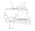
- FIG. 2 is a view of an exposure apparatus according to the first and second embodiments.
- the figure of the chuck concerning a 1st embodiment (at the time of substrate carrying out).
- the configuration of the exposure apparatus 1 according to the first embodiment will be described with reference to FIG.
- the exposure apparatus 1 irradiates the i-line (wavelength 365 nm) while scanning the reticle 2 and the substrate 3 by the step-and-repeat method, and the pattern (for example, circuit pattern etc.) formed on the reticle 2 is 3 is a projection type exposure apparatus which transfers the image onto the image forming apparatus 3;
- an axis parallel to the optical axis (vertical direction in the present embodiment) of the projection optical system 4 is taken as a Z axis.
- the direction in which the reticle 2 scans during exposure is taken as an X axis
- the non-scanning direction orthogonal to the X axis is taken as a Y axis.
- the illumination light (beam) 6 formed by the illumination optical system 5 is irradiated onto the substrate 3 via the reticle 2 and the projection optical system 4.
- the substrate 3 is, for example, a substrate of single crystal silicon, and a resist is applied on the surface.
- the reticle 2 moves with the stage 7.
- the interferometer 8 irradiates the mirror 9 with a laser beam and receives the reflected light to detect the position of the stage 7.
- the stage 7 has a stage top plate for a reticle (not shown) and a moving mechanism (not shown) for moving the stage top plate for the reticle.
- the substrate 3 moves in six axial directions together with a holding device 10 for holding the substrate 3 by vacuum suction and a stage 13.
- the interferometer 11 uses the mirror 12 to detect the position of the stage 13 in the same manner as the position detection of the stage 7.
- the stage 13 has a stage top plate (not shown) for a substrate and a moving mechanism (not shown) for moving the stage top plate for the substrate.
- the detection system 14 detects an alignment mark (not shown) formed on the substrate 3 and a reference mark (not shown) formed on the mark table 15 installed on the stage 13.
- the detection system 14 detects the position of the alignment mark and the reference mark, and the formation position of the pattern is determined by the control unit 18 described later.
- an off-axis alignment detection system that detects the alignment mark and the reference mark without using the projection optical system 4 is adopted.
- the holding device (substrate holding device) 10 raises and lowers a chuck (holding member) 16 for holding the substrate 3, a pin 17 for supporting the substrate 3 at the time of loading and unloading of the substrate 3, and the chuck 16 along the Z-axis direction. And a lifting mechanism (not shown).
- the substrate 3 is delivered from the pin 17 to the chuck 16 at the time of loading, and from the chuck 16 to the pin 17 at the unloading by the elevating operation of the chuck 16.
- the configuration of the holding device 10 will be described in detail later.
- the control unit 18 is connected to the stages 7 and 13, the detection system 14, the interferometers 8 and 11, and the holding device 10 via a wire, and integrally controls them. For example, at the time of exposure processing, the formation position of the pattern is determined based on the detection result of the detection system 14, and the movement of the stages 7 and 13 is controlled based on the position information obtained from the interferometers 8 and 11. In addition, at the time of loading and unloading of the substrate 3, the movement mechanism of the chuck 16 and the movement of the stage 13 are controlled.
- the control unit 18 may be configured in a housing that accommodates components other than the control unit 18, or may be configured in a housing different from the housing.
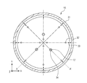
- FIG. 2 is a view of the holding device 10 as seen from the + Z direction.
- the holding device 10 has a chuck 16 having a circular shape when viewed in the + Z direction.
- suction holes (intake holes) 32, open holes (holes) 33, and pin holes 34 are formed concentrically.
- the pin holes 34 are formed to penetrate three places near the center of the chuck 16 respectively.
- the pin 17 protrudes from the inside of the pin hole 34, and the pin 17 serves as a support for loading and unloading the substrate 3.
- the gap between the pin 17 and the pin hole 34 is closed with a sealing material (not shown) or the like, so that no leak occurs.
- the suction holes 32 are formed at four places on the central side of the chuck 16 and at five places on the outer peripheral side of the four suction holes 32.
- the adsorption holes 32 are connected to a pipe 35 (shown in FIG. 3) which is an exhaust system and a vacuum pump (not shown).
- the open holes 33 are formed on the outer peripheral side of the suction holes 32 at two positions at eight positions per one rotation.
- An annular lip seal (seal member) 31 formed of an elastic material is fixed on the chuck 16 along the outer edge of the chuck 16.
- FIGS. 3A and 3B are cross-sectional views in the XZ plane passing through the center of the chuck 16.
- FIG. 3A shows a state in which the substrate 3 has been carried in to the substrate loading position, which is the height position when the substrate 3 is placed on the holding device 10 before the start of evacuation above the chuck 16. .
- the range of the space 42 between the substrate 3 and the chuck 16 (the space between the substrate) is defined by being surrounded by the lip seal 31.
- the chuck 16 includes a central portion 40 in contact with the substrate 3 when the substrate 3 is adsorbed, and an outer peripheral portion 41 surrounding the central portion 40 and formed at a position lower in height than the central portion 40. That is, the distance from the substrate loading position to the surface of the outer peripheral portion 41 is larger than the distance from the substrate loading position to the surface of the central portion 40.
- a lip seal 31 is disposed in the peripheral portion 41.
- the central portion 40 also includes a plurality of pins (not shown) formed to reduce the contact area with the substrate 3 and an annular convex structure (not shown) for auxiliary sealing of the space 42. It may be.
- the suction holes 32 are formed on the surface of the central portion 40.
- the suction holes 32 are combined into one exhaust flow path including the pipe 35 inside the chuck 16, and are connected to the pipe 35 on the lower surface side of the chuck 16.
- the valve 36 is in the pipe 35 connecting the suction hole 32 and the vacuum pump.
- the open hole 33 is formed so as to penetrate the chuck 16 in the vertical direction (direction along the thickness direction of the holding member) as shown in FIG. 3A.
- the open hole 33 has an opening at one end facing the space 42 and an opening at the other end facing the atmospheric space, and is an independent air passage from the piping 35 which is an exhaust system.
- the diameter of the open hole 33 is formed to be smaller than the diameter of the suction hole 32.
- FIG. 3B shows a state in which the substrate 3 is adsorbed to the chuck 16 after the start of the evacuation. By exhausting the space 42, the pressure in the space 42 is reduced, and the lip seal 31 is deformed according to the change in position of the substrate 3.
- the lip seal 31 is fixed to the outer peripheral portion 41 using a bonding agent such as an adhesive sheet.
- the non-fixed tip contacts at a position along the outer periphery of the substrate 3.
- the lip seal 31 deforms as the substrate 3 is attracted, the space 42 surrounded by the chuck 16, the lip seal 31 and the substrate 3 is sealed.
- the lip seal 31 be a soft member which is easily deformed and expandable. It is preferable to use a polymer material (elastic polymer material) containing a synthetic rubber such as silicone rubber and fluorine rubber (material containing a fluorine compound), but other soft resin or metal material may be used.
- a polymer material elastic polymer material
- a synthetic rubber such as silicone rubber and fluorine rubber (material containing a fluorine compound)
- other soft resin or metal material may be used.
- the substrate 3 receives the atmospheric pressure and is adsorbed so as to follow the central portion of the chuck 16. Thereby, planar correction of the substrate 3 can be performed. In addition, even when the edge of the substrate 3 is warped, the warp can be corrected.
- the exposure apparatus 1 performs an exposure process. After completion of the exposure, the holding device 13 is controlled to bring the substrate 3 out of the state.
- FIG. 4A is a cross-sectional view of the chuck 16 taken along the dotted line A-A 'in FIG.
- the elevating mechanism lowers the chuck 16
- the substrate 3 is transferred from the surface of the chuck 16 to the pin 17, and the pin 17 relatively protrudes the chuck 16.
- the space 42 becomes negative pressure with respect to the atmospheric pressure.
- the atmosphere can be positively introduced into the space vertically above the outer peripheral portion 41 including the contact portion between the substrate 3 and the lip seal 31 and having the largest volume of the exhaust space.
- the air passage through the open hole 33 has a short length and is not a space evacuated by a vacuum pump like the pipe 35, so that air can be supplied in a short time. Thereby, the substrate 3 can be pulled away from the lip seal 31 in a short time.
- an open hole 33 independent of the exhaust system be formed in the outer peripheral portion. Moreover, it is preferable that it is a through-hole formed along the thickness direction of the chuck
- the open hole 33 of the present embodiment can supply the space 42 with a necessary amount of air according to the pressure difference between the space 42 and the air space.
- the open hole 33 is at least on the outer peripheral portion 41 so that the air can be efficiently supplied to the contact portion of the lip seal 31 and the substrate 3 It is preferable to provide.
- air can be supplied in a short time by making the open hole 33 independent from the exhaust system and shortening the flow path of air from the atmospheric space to the space 42.
- the sum of the cross-sectional areas of the open hole (second hole) 33 formed in the central portion 40 and the open hole (first hole) 33 formed in the outer peripheral portion 41 is the space 42.
- the cross-sectional area in the direction along the substrate holding surface is preferably 0.03% or less. More preferably, it is good to be 0.0005% or more and 0.004% or less. As a result, it is possible to achieve both the suppression of leakage at the time of suction of the substrate 3 and the shortening of the time taken at the time of unloading the substrate 3.
- the substrate holding surface means the substrate side surface of the central portion, and the cross sectional area of the space 42 in the direction along the substrate holding surface means the cross sectional area of the surface formed by the inner diameter of the lip seal 31.
- the tip of the lip seal 31 (for example, a portion having a height of 1/3 from the tip of the lip seal 31) be a material with low adhesiveness.
- the above-mentioned fluororubber material containing a fluorine compound
- at least the tip may be coated with PTFE, molybdenum disulfide or the like, which is a material with low adhesiveness.
- the substrate 3 By lowering the adhesiveness, the substrate 3 can be easily separated from the lip seal 31. This can reduce the time taken for unloading. Further, the wear of the surface of the lip seal 31 at the contact portion with the substrate 3 can be reduced to extend the durable life of the lip seal 31, and particles generated by the wear can be prevented from scattering into the apparatus.
- Example 2 An example of the first embodiment will be described.
- the substrate 3 having a diameter of 300 mm was used.
- a chuck having an open hole 33 and a chuck having no open hole 33 were prepared.
- An open hole 33 with a diameter of 0.3 mm was formed in the chuck 16 having the open hole 33 so that the total cross-sectional area would be 1.5 mm 2 .
- the unloading operation was repeated while changing the lowering speed of the chuck 16 after the substrate 3 was in contact with the pin 17, and the lowering speeds at which the positional deviation of the substrate 3 occurred were compared.
- the lowering speed of the chuck 16 until the substrate 3 was transferred from the central portion 40 to the pin 17 was common to both of the chucks.
- the contribution to productivity is calculated by setting the lowering distance of the chuck 16 from the contact of the substrate 3 with the pin 17 to the release from the lip seal 13 as 1 mm.
- the lowering speed of the chuck 16 can be 1.0 mm / s due to the presence of the open hole 33, the unloading process per sheet of the substrate 3 is accelerated by 4 seconds.
- the processing speed of the chuck without the open hole 33 is 150 sheets / h, whereas the processing speed of the chuck with the open hole 33 is 180 sheets / h. That is, the productivity for 30 sheets will be improved.
- FIG. 5 is a cross-sectional view of the chuck 16 according to the fourth embodiment.
- the open hole 43 is formed at a position (a lead-in area of the seal member) 44 which is closed by the lip seal 31 drawn to the space 42 side when the substrate 3 is sucked, in the substrate facing surface of the outer peripheral portion. This has the effect of reducing the leak from the open hole 43 while the substrate 3 is adsorbed.
- FIG. 6 is a cross-sectional view of the chuck 16 according to the third embodiment.
- an open hole 33 which is not connected to the pipe 35 connected to the vacuum pump is formed.
- the pipe connected to the open hole 33 is provided with a valve 37 which is an openable and closable solenoid valve, and a control unit 38 connected to the valve 37 controls the opening and closing of the valve 37.
- the other configuration is the same as that of the chuck 16 of the first embodiment.
- the controller 38 closes the valve 37 when the substrate 3 is adsorbed, and opens the valve 37 when the substrate 3 is unloaded.
- the length of the pipe to be replaced by air at the time of carrying out the substrate 3 to supply the air from the open hole 33 is shorter than the length of the pipe when connected with the vacuum pump. 3 can be released from the lip seal 31. Furthermore, it is possible to suppress the inflow of air into the space 42 through the open hole 33 during adsorption of the substrate 3.
- FIG. 7 is a cross-sectional view of the chuck 16 according to the fourth embodiment.
- an open hole 33 which is not connected to the pipe 35 connected to the vacuum pump is formed.
- a valve 37 which is an electromagnetic valve that can be opened and closed, is provided between the open hole 33 and the compressed air supply source (gas supply source) 39, and the control unit 38 connected to the valve 37 opens and closes the valve 37. Control.
- the other configuration is the same as that of the chuck 16 of the first embodiment.
- the pressure in the space 42 is detected by a pressure sensor (not shown), and the control unit 38 controls the flow rate of air (gas) passing through the hole 33 based on the detection result.
- the control unit 38 has a function as a flow rate control unit.
- the compressed air can efficiently supply the atmosphere, and the controller 38 supplies the atmosphere while adjusting the flow rate to prevent the pressure in the space 42 from becoming higher than the atmospheric pressure.
- the controller 38 supplies the atmosphere while adjusting the flow rate to prevent the pressure in the space 42 from becoming higher than the atmospheric pressure.
- the length of the pipe to be replaced by air at the time of carrying out the substrate 3 to supply the air from the open hole 33 is shorter than the length of the pipe when connected with the vacuum pump. 3 can be released from the lip seal 31.
- the pressure sensor is not essential.
- the control unit 38 may control the pressure of the air supplied to the space 42 based on the degree of expansion of the air in the space 42 calculated from the predetermined lowering speed of the chuck 16. Further, a valve (not shown) for letting air out may be provided on the chuck 16 in preparation for the case where the pressure in the space 42 becomes higher than the atmospheric pressure.
- One of the open holes 33 may face the space 42 and the other may face the atmospheric space. Therefore, the open hole 33 may be formed in at least one of the outer peripheral portion of the chuck 16 and the lip seal 31.
- FIG. 8 is a view of the holding device 10 in which the opening hole 33 is formed on the lip seal 31.
- the lip seal 31 may be fixed by another component so that replacement of the lip seal 31 is facilitated.
- the lip seal 31 may be divided into a tip portion including a portion in contact with the substrate 3 and the other portion so that only the worn tip portion may be replaced.
- the open hole 33 is preferably a hole having a larger cross-sectional area as it is located farther from the center of the chuck 16. Since most of the space 42 is a space on the outer periphery during adsorption of the substrate 3, it is easier to separate the substrate 3 from the lip seal 31 in a short time by supplying the gas preferentially to the outer peripheral side. . For example, when the central area and the area outside the central area of the same area on the substrate holding surface are set and the same number of holes are provided in each area, the holes in the outer area It is good to increase the total cross-sectional area.
- the open holes 33 may not necessarily be arranged at equal angular intervals. When the suction holes 32 or the vacuum pump is disposed at a position offset to the chuck 16, the number of the open holes 33 may be increased in a region where the density of the suction holes 32 is small.
- the substrate 3 may be shifted by about 10 to 1000 ⁇ m in the predetermined direction before and after the substrate 3 is sucked. This is due to individual differences and mounting errors caused by the manufacturing process of the lip seal 31.
- the positional deviation is measured in advance using the detection system 8 before the start of exposure, the correction amount is calculated by the arithmetic circuit of the control unit 18 or the like, and the stages 7 and 13 are scanned considering the correction amount. It is possible to reduce the positional deviation of the substrate 3 caused by the suction operation and to prevent the lowering of the overlay accuracy.
- the light emitted to the substrate 3 by the lithography apparatus of the present invention is not limited to the i-line (wavelength 365 nm). It may be light in the far ultraviolet region such as KrF light (wavelength 248 nm) or ArF light (wavelength 193 nm), or g-line (wavelength 436 nm) which is light in the visible light region.
- the lithography apparatus of the present invention may be an apparatus for forming a latent image pattern on a wafer by irradiating a charged particle beam to the substrate or an apparatus for forming a pattern on the substrate by an imprint method.
- a method of manufacturing an article (a semiconductor integrated circuit device, a liquid crystal display device, an imaging device, a magnetic head, a CD-RW, an optical device, a photomask, etc.) according to an embodiment of the present invention And exposing the exposed substrate to at least one of an etching process and an ion implantation process. Furthermore, other known processing steps (developing, oxidation, film formation, vapor deposition, planarization, resist peeling, dicing, bonding, packaging, etc.) may be included.
- Exposure system (lithography system) 3 Substrate 16 Chuck (holding member) 31 Lip seal (seal member) 32 suction holes (intake holes) 33 Open hole (hole) 40 central part 41 outer peripheral part 42 space 43 open hole (hole)
Abstract
Priority Applications (5)
| Application Number | Priority Date | Filing Date | Title |
|---|---|---|---|
| CN201480083967.9A CN107004574B (zh) | 2014-12-12 | 2014-12-12 | 基板保持装置、光刻设备以及物品制造方法 |
| KR1020177018429A KR102005649B1 (ko) | 2014-12-12 | 2014-12-12 | 기판 유지 장치, 리소그래피 장치, 및 물품의 제조 방법 |
| PCT/JP2014/082986 WO2016092700A1 (fr) | 2014-12-12 | 2014-12-12 | Appareil de maintien de substrat, appareil de lithographie et procédé de fabrication d'articles |
| JP2016563378A JP6400120B2 (ja) | 2014-12-12 | 2014-12-12 | 基板保持装置、リソグラフィ装置、及び物品の製造方法 |
| US14/963,656 US10431463B2 (en) | 2014-12-12 | 2015-12-09 | Substrate holding device, lithography apparatus, and article production method |
Applications Claiming Priority (1)
| Application Number | Priority Date | Filing Date | Title |
|---|---|---|---|
| PCT/JP2014/082986 WO2016092700A1 (fr) | 2014-12-12 | 2014-12-12 | Appareil de maintien de substrat, appareil de lithographie et procédé de fabrication d'articles |
Publications (2)
| Publication Number | Publication Date |
|---|---|
| WO2016092700A1 true WO2016092700A1 (fr) | 2016-06-16 |
| WO2016092700A9 WO2016092700A9 (fr) | 2017-05-04 |
Family
ID=56106944
Family Applications (1)
| Application Number | Title | Priority Date | Filing Date |
|---|---|---|---|
| PCT/JP2014/082986 WO2016092700A1 (fr) | 2014-12-12 | 2014-12-12 | Appareil de maintien de substrat, appareil de lithographie et procédé de fabrication d'articles |
Country Status (5)
| Country | Link |
|---|---|
| US (1) | US10431463B2 (fr) |
| JP (1) | JP6400120B2 (fr) |
| KR (1) | KR102005649B1 (fr) |
| CN (1) | CN107004574B (fr) |
| WO (1) | WO2016092700A1 (fr) |
Cited By (4)
| Publication number | Priority date | Publication date | Assignee | Title |
|---|---|---|---|---|
| KR20180134292A (ko) * | 2017-06-08 | 2018-12-18 | 가부시기가이샤 디스코 | 척테이블 |
| KR20190058664A (ko) * | 2016-10-19 | 2019-05-29 | 케이엘에이-텐코 코포레이션 | 휘어진 웨이퍼를 척킹하기 위한 방법 및 시스템 |
| JP2021061328A (ja) * | 2019-10-07 | 2021-04-15 | キヤノン株式会社 | 型を用いて基板上の組成物を成形する成形装置、成形方法、及び、物品製造方法 |
| JP2022083762A (ja) * | 2020-11-25 | 2022-06-06 | 株式会社ブイ・テクノロジー | 露光装置及び露光方法 |
Families Citing this family (5)
| Publication number | Priority date | Publication date | Assignee | Title |
|---|---|---|---|---|
| US20170053822A1 (en) * | 2015-08-23 | 2017-02-23 | Camtek Ltd. | Warped wafers vacuum chuck |
| KR101926726B1 (ko) * | 2018-06-28 | 2018-12-07 | 주식회사 기가레인 | 부산물 증착 문제가 개선된 립실 및 이를 포함하는 반도체 공정 장치 |
| EP3864690A1 (fr) * | 2018-10-10 | 2021-08-18 | Nordson Corporation | Appareil et procédé de serrage sous vide |
| US11567417B2 (en) * | 2021-01-20 | 2023-01-31 | Applied Materials, Inc. | Anti-slippery stamp landing ring |
| EP4227738A1 (fr) * | 2022-02-14 | 2023-08-16 | ASML Netherlands B.V. | Pince |
Citations (9)
| Publication number | Priority date | Publication date | Assignee | Title |
|---|---|---|---|---|
| JPH0582631A (ja) * | 1991-09-20 | 1993-04-02 | Toshiba Ceramics Co Ltd | 半導体ウエーハ用真空チヤツク |
| JPH07284716A (ja) * | 1994-04-18 | 1995-10-31 | Sony Corp | スピンコータ及びそのスピンコータにおける回転板保持方法 |
| JP2001215716A (ja) * | 2000-02-02 | 2001-08-10 | Orc Mfg Co Ltd | ワークとマスクの分離機構 |
| JP2002217276A (ja) * | 2001-01-17 | 2002-08-02 | Ushio Inc | ステージ装置 |
| JP2003051535A (ja) * | 2001-08-07 | 2003-02-21 | Canon Inc | 基板保持装置、露光装置およびデバイス製造方法 |
| WO2006100842A1 (fr) * | 2005-03-03 | 2006-09-28 | Fujifilm Corporation | Mecanisme de maintien de feuilles et appareil de lithographie l'utilisant |
| JP2006310697A (ja) * | 2005-05-02 | 2006-11-09 | Dainippon Screen Mfg Co Ltd | 吸着チャック |
| JP2007158077A (ja) * | 2005-12-06 | 2007-06-21 | Dainippon Screen Mfg Co Ltd | 基板熱処理装置 |
| JP2010197415A (ja) * | 2009-02-22 | 2010-09-09 | Ushio Inc | ワークステージ及びそのワークステージを備えた露光装置 |
Family Cites Families (13)
| Publication number | Priority date | Publication date | Assignee | Title |
|---|---|---|---|---|
| NL8701603A (nl) * | 1987-07-08 | 1989-02-01 | Philips & Du Pont Optical | Vacuuminrichting voor het vastzuigen van werkstukken. |
| JPH0851143A (ja) * | 1992-07-20 | 1996-02-20 | Nikon Corp | 基板保持装置 |
| KR100588124B1 (ko) * | 2002-11-12 | 2006-06-09 | 에이에스엠엘 네델란즈 비.브이. | 리소그래피장치 및 디바이스제조방법 |
| KR101528089B1 (ko) * | 2003-06-13 | 2015-06-11 | 가부시키가이샤 니콘 | 노광 방법, 기판 스테이지, 노광 장치, 및 디바이스 제조 방법 |
| JP4407333B2 (ja) * | 2004-03-23 | 2010-02-03 | ウシオ電機株式会社 | 帯状ワークの露光装置 |
| JP2006120889A (ja) * | 2004-10-22 | 2006-05-11 | Sony Corp | 半導体装置の製造方法及びその方法に用いられる半導体ウェハホルダ |
| US7230681B2 (en) * | 2004-11-18 | 2007-06-12 | International Business Machines Corporation | Method and apparatus for immersion lithography |
| KR101585310B1 (ko) * | 2004-12-15 | 2016-01-14 | 가부시키가이샤 니콘 | 기판 유지 장치, 노광 장치 및 디바이스 제조방법 |
| KR101539517B1 (ko) * | 2005-12-08 | 2015-07-24 | 가부시키가이샤 니콘 | 노광 장치, 노광 방법 및 디바이스 제조 방법 |
| KR100689843B1 (ko) * | 2006-01-03 | 2007-03-08 | 삼성전자주식회사 | 웨이퍼 스테이지 및 이를 이용한 웨이퍼 안착방법 |
| US8705010B2 (en) * | 2007-07-13 | 2014-04-22 | Mapper Lithography Ip B.V. | Lithography system, method of clamping and wafer table |
| AT511627B1 (de) * | 2011-07-01 | 2015-05-15 | Mechatronic Systemtechnik Gmbh | Vorrichtung zum halten eines flächigen substrats |
| GB2502303A (en) * | 2012-05-22 | 2013-11-27 | Applied Microengineering Ltd | Method of handling a substrate using a pressure variance |
-
2014
- 2014-12-12 WO PCT/JP2014/082986 patent/WO2016092700A1/fr active Application Filing
- 2014-12-12 JP JP2016563378A patent/JP6400120B2/ja active Active
- 2014-12-12 CN CN201480083967.9A patent/CN107004574B/zh active Active
- 2014-12-12 KR KR1020177018429A patent/KR102005649B1/ko active IP Right Grant
-
2015
- 2015-12-09 US US14/963,656 patent/US10431463B2/en active Active
Patent Citations (9)
| Publication number | Priority date | Publication date | Assignee | Title |
|---|---|---|---|---|
| JPH0582631A (ja) * | 1991-09-20 | 1993-04-02 | Toshiba Ceramics Co Ltd | 半導体ウエーハ用真空チヤツク |
| JPH07284716A (ja) * | 1994-04-18 | 1995-10-31 | Sony Corp | スピンコータ及びそのスピンコータにおける回転板保持方法 |
| JP2001215716A (ja) * | 2000-02-02 | 2001-08-10 | Orc Mfg Co Ltd | ワークとマスクの分離機構 |
| JP2002217276A (ja) * | 2001-01-17 | 2002-08-02 | Ushio Inc | ステージ装置 |
| JP2003051535A (ja) * | 2001-08-07 | 2003-02-21 | Canon Inc | 基板保持装置、露光装置およびデバイス製造方法 |
| WO2006100842A1 (fr) * | 2005-03-03 | 2006-09-28 | Fujifilm Corporation | Mecanisme de maintien de feuilles et appareil de lithographie l'utilisant |
| JP2006310697A (ja) * | 2005-05-02 | 2006-11-09 | Dainippon Screen Mfg Co Ltd | 吸着チャック |
| JP2007158077A (ja) * | 2005-12-06 | 2007-06-21 | Dainippon Screen Mfg Co Ltd | 基板熱処理装置 |
| JP2010197415A (ja) * | 2009-02-22 | 2010-09-09 | Ushio Inc | ワークステージ及びそのワークステージを備えた露光装置 |
Cited By (7)
| Publication number | Priority date | Publication date | Assignee | Title |
|---|---|---|---|---|
| KR20190058664A (ko) * | 2016-10-19 | 2019-05-29 | 케이엘에이-텐코 코포레이션 | 휘어진 웨이퍼를 척킹하기 위한 방법 및 시스템 |
| KR102442238B1 (ko) * | 2016-10-19 | 2022-09-08 | 케이엘에이 코포레이션 | 휘어진 웨이퍼를 척킹하기 위한 방법 및 시스템 |
| KR20180134292A (ko) * | 2017-06-08 | 2018-12-18 | 가부시기가이샤 디스코 | 척테이블 |
| JP2018207033A (ja) * | 2017-06-08 | 2018-12-27 | 株式会社ディスコ | チャックテーブル |
| KR102515856B1 (ko) * | 2017-06-08 | 2023-03-29 | 가부시기가이샤 디스코 | 척테이블 |
| JP2021061328A (ja) * | 2019-10-07 | 2021-04-15 | キヤノン株式会社 | 型を用いて基板上の組成物を成形する成形装置、成形方法、及び、物品製造方法 |
| JP2022083762A (ja) * | 2020-11-25 | 2022-06-06 | 株式会社ブイ・テクノロジー | 露光装置及び露光方法 |
Also Published As
| Publication number | Publication date |
|---|---|
| US20160170313A1 (en) | 2016-06-16 |
| KR20170094281A (ko) | 2017-08-17 |
| CN107004574B (zh) | 2020-06-30 |
| KR102005649B1 (ko) | 2019-10-01 |
| WO2016092700A9 (fr) | 2017-05-04 |
| US10431463B2 (en) | 2019-10-01 |
| CN107004574A (zh) | 2017-08-01 |
| JP6400120B2 (ja) | 2018-10-03 |
| JPWO2016092700A1 (ja) | 2017-10-19 |
Similar Documents
| Publication | Publication Date | Title |
|---|---|---|
| WO2016092700A1 (fr) | Appareil de maintien de substrat, appareil de lithographie et procédé de fabrication d'articles | |
| JP6732429B2 (ja) | 基板保持装置、リソグラフィ装置、及び物品の製造方法 | |
| TWI607519B (zh) | 吸引裝置、搬入方法、搬送系統及曝光裝置、以及元件製造方法 | |
| TWI770500B (zh) | 基板保持裝置、曝光裝置及元件製造方法 | |
| US9740109B2 (en) | Holding device, lithography apparatus, and method for manufacturing item | |
| JP2007273693A (ja) | 基板保持部材及び基板保持方法、基板保持装置、並びに露光装置及び露光方法 | |
| US20210223696A1 (en) | Substrate, a substrate holder, a substrate coating apparatus, a method for coating the substrate and a method for removing the coating | |
| JP2010129929A (ja) | 基板保持装置、基板保持方法、露光装置およびデバイス製造方法 | |
| WO2017209051A1 (fr) | Mandrin, dispositif de support de substrat, dispositif de formation de motif et procédé de fabrication d'article | |
| JP5656392B2 (ja) | 基板保持装置、それを用いた露光装置、及びデバイスの製造方法 | |
| JP4298739B2 (ja) | 基板吸着装置 | |
| JP2014003259A (ja) | ロード方法、基板保持装置及び露光装置 | |
| TWI754333B (zh) | 基板固持器、微影設備及方法 | |
| JP4298740B2 (ja) | 基板吸着装置 | |
| JP2004221296A (ja) | 基板保持装置及び露光装置、並びにデバイス製造方法 | |
| KR20080044783A (ko) | 리소그래피 장치 및 디바이스 제조 방법 | |
| WO2007139017A1 (fr) | Élément de récupération de liquide, appareil de support de substrat, appareil d'exposition et procédé de fabrication du dispositif | |
| JP6086292B2 (ja) | 基板保持装置及び露光装置 | |
| JP2015222778A (ja) | 保持装置、リソグラフィ装置、および物品の製造方法 | |
| TWI810443B (zh) | 基板保持裝置、光刻裝置及物品之製造方法 | |
| JP2017033021A (ja) | 保持装置及び保持方法、露光装置及び露光方法、並びにデバイス製造方法 | |
| JP6844804B1 (ja) | 露光装置及び露光方法 | |
| JP2014138078A (ja) | 搬送システム及び搬送方法、露光装置及び露光方法、並びにデバイス製造方法 | |
| JP6702753B2 (ja) | リソグラフィ装置、及び物品の製造方法 | |
| JP2014138004A (ja) | 保持装置及び保持方法、露光装置及び露光方法、並びにデバイス製造方法 |
Legal Events
| Date | Code | Title | Description |
|---|---|---|---|
| 121 | Ep: the epo has been informed by wipo that ep was designated in this application |
Ref document number: 14907631 Country of ref document: EP Kind code of ref document: A1 |
|
| ENP | Entry into the national phase |
Ref document number: 2016563378 Country of ref document: JP Kind code of ref document: A |
|
| NENP | Non-entry into the national phase |
Ref country code: DE |
|
| ENP | Entry into the national phase |
Ref document number: 20177018429 Country of ref document: KR Kind code of ref document: A |
|
| 122 | Ep: pct application non-entry in european phase |
Ref document number: 14907631 Country of ref document: EP Kind code of ref document: A1 |