WO2016006442A1 - 炭化珪素単結晶の製造方法および炭化珪素基板 - Google Patents
炭化珪素単結晶の製造方法および炭化珪素基板 Download PDFInfo
- Publication number
- WO2016006442A1 WO2016006442A1 PCT/JP2015/068162 JP2015068162W WO2016006442A1 WO 2016006442 A1 WO2016006442 A1 WO 2016006442A1 JP 2015068162 W JP2015068162 W JP 2015068162W WO 2016006442 A1 WO2016006442 A1 WO 2016006442A1
- Authority
- WO
- WIPO (PCT)
- Prior art keywords
- support member
- crystal
- single crystal
- silicon carbide
- diameter
- Prior art date
- Legal status (The legal status is an assumption and is not a legal conclusion. Google has not performed a legal analysis and makes no representation as to the accuracy of the status listed.)
- Ceased
Links
Images



Classifications
-
- C—CHEMISTRY; METALLURGY
- C30—CRYSTAL GROWTH
- C30B—SINGLE-CRYSTAL GROWTH; UNIDIRECTIONAL SOLIDIFICATION OF EUTECTIC MATERIAL OR UNIDIRECTIONAL DEMIXING OF EUTECTOID MATERIAL; REFINING BY ZONE-MELTING OF MATERIAL; PRODUCTION OF A HOMOGENEOUS POLYCRYSTALLINE MATERIAL WITH DEFINED STRUCTURE; SINGLE CRYSTALS OR HOMOGENEOUS POLYCRYSTALLINE MATERIAL WITH DEFINED STRUCTURE; AFTER-TREATMENT OF SINGLE CRYSTALS OR A HOMOGENEOUS POLYCRYSTALLINE MATERIAL WITH DEFINED STRUCTURE; APPARATUS THEREFOR
- C30B23/00—Single-crystal growth by condensing evaporated or sublimed materials
- C30B23/02—Epitaxial-layer growth
- C30B23/06—Heating of the deposition chamber, the substrate or the materials to be evaporated
-
- C—CHEMISTRY; METALLURGY
- C30—CRYSTAL GROWTH
- C30B—SINGLE-CRYSTAL GROWTH; UNIDIRECTIONAL SOLIDIFICATION OF EUTECTIC MATERIAL OR UNIDIRECTIONAL DEMIXING OF EUTECTOID MATERIAL; REFINING BY ZONE-MELTING OF MATERIAL; PRODUCTION OF A HOMOGENEOUS POLYCRYSTALLINE MATERIAL WITH DEFINED STRUCTURE; SINGLE CRYSTALS OR HOMOGENEOUS POLYCRYSTALLINE MATERIAL WITH DEFINED STRUCTURE; AFTER-TREATMENT OF SINGLE CRYSTALS OR A HOMOGENEOUS POLYCRYSTALLINE MATERIAL WITH DEFINED STRUCTURE; APPARATUS THEREFOR
- C30B29/00—Single crystals or homogeneous polycrystalline material with defined structure characterised by the material or by their shape
- C30B29/10—Inorganic compounds or compositions
- C30B29/36—Carbides
-
- C—CHEMISTRY; METALLURGY
- C30—CRYSTAL GROWTH
- C30B—SINGLE-CRYSTAL GROWTH; UNIDIRECTIONAL SOLIDIFICATION OF EUTECTIC MATERIAL OR UNIDIRECTIONAL DEMIXING OF EUTECTOID MATERIAL; REFINING BY ZONE-MELTING OF MATERIAL; PRODUCTION OF A HOMOGENEOUS POLYCRYSTALLINE MATERIAL WITH DEFINED STRUCTURE; SINGLE CRYSTALS OR HOMOGENEOUS POLYCRYSTALLINE MATERIAL WITH DEFINED STRUCTURE; AFTER-TREATMENT OF SINGLE CRYSTALS OR A HOMOGENEOUS POLYCRYSTALLINE MATERIAL WITH DEFINED STRUCTURE; APPARATUS THEREFOR
- C30B23/00—Single-crystal growth by condensing evaporated or sublimed materials
- C30B23/02—Epitaxial-layer growth
- C30B23/025—Epitaxial-layer growth characterised by the substrate
Definitions
- the present disclosure relates to a method for manufacturing a silicon carbide single crystal and a silicon carbide substrate.
- a method for manufacturing a silicon carbide single crystal includes a step of preparing a bonding member and a support member having a stepped portion at least at a part of the periphery of the bonding portion, and a buffer material in the stepped portion. And a step of arranging the seed crystal on the support surface, and adhering the bond portion and the seed crystal to each other. And growing a single crystal on the seed crystal.
- a silicon carbide substrate according to one embodiment of the present disclosure has a central region that has a diameter of 150 mm or more and a diameter of 50 mm, and an outer peripheral region that is formed along the outer peripheral end and has a distance of 10 mm or less from the outer peripheral end.
- the crystal plane orientation measured at any three points in the central region is averaged as the reference orientation, and the crystal plane orientation measured at any point in the outer peripheral region and the reference orientation The deviation is 200 arcsec or less.
- the sublimation method is a crystal growth method in which a raw material is sublimated at a high temperature and the sublimated raw material is recrystallized on a seed crystal.
- the raw material is accommodated in the lower part of a growth vessel (for example, a graphite crucible), and the seed crystal is bonded and fixed to a support member (for example, a crucible lid) located at the upper part of the growth vessel.
- a growth vessel for example, a graphite crucible
- a support member for example, a crucible lid
- Patent Document 1 proposes disposing a stress buffer material between a seed crystal and a pedestal (support member) in the sublimation method. According to this, since the stress buffer material relieves the thermal stress caused by the difference in thermal expansion coefficient between the seed crystal and the pedestal, the lattice plane warpage and macro defects can be prevented in the grown SiC single crystal. Has been.
- Patent Document 2 it is proposed that a buffer member is interposed between the seed crystal and the pedestal, and that the buffer member is connected to the pedestal without using an adhesive. According to this, it is said that the curvature of the lattice plane of the grown crystal can be prevented by allowing the warping of the buffer member due to the difference in thermal expansion coefficient between the seed crystal and the buffer member.
- the graphite sheet used as the stress buffer material or the buffer member has a structure in which graphite layers are laminated in layers.
- Such a graphite sheet exhibits high thermal conductivity in the in-plane direction of the graphite layer (in-plane direction of the sheet), but has a relatively low thermal conductivity in the stacking direction of the graphite layer (sheet thickness direction).
- the thermal conductivity in the in-plane direction is about 134 W / (m ⁇ K)
- the thermal conductivity in the stacking direction is only about 4.7 W / (m ⁇ K).
- the graphite sheet has low thermal conductivity in the thickness direction in this way, if a graphite sheet is interposed between the seed crystal and the pedestal, a large temperature difference occurs in the thickness direction of the graphite sheet, resulting in growth. The temperature difference between the crystal and the raw material becomes small, and the crystal growth rate decreases.
- the above method lacks production stability. That is, when the seed crystal is bonded and fixed to the graphite sheet, the seed crystal may be peeled off from the pedestal and dropped. This is because the fracture strength between the graphite layers is low in the graphite sheet, and the mass of the grown crystal increases, or thermal stress due to the difference in thermal expansion coefficient between the seed crystal and the graphite sheet occurs easily between the layers. This is because it will break. Even if it does not fall, if even part of the detachment occurs between the pedestal and the seed crystal, the seed crystal (SiC) will sublimate to the lower temperature side (the pedestal side) at that part, resulting in growth. Fine through holes are formed in the crystal. Such an event is particularly prominent when growing large-diameter single crystals.
- a method for manufacturing a silicon carbide single crystal includes a step of preparing a support member having an adhesive portion and a step portion at least at a part of the periphery of the adhesive portion; A step of disposing a buffer material, wherein the bonding portion and the buffer material constitute a support surface, and a seed crystal is disposed on the support surface, and the bonding portion and the seed crystal are bonded to each other. And a step of growing a single crystal on the seed crystal.
- a SiC substrate having a large diameter (for example, a diameter of 150 mm or more) can be manufactured.
- the seed crystal is directly bonded to the support member at the bonding portion.
- the seed crystal can be stably held without causing problems such as dropping.
- no buffer material is interposed in the bonded portion, a large temperature difference does not occur between the support member and the seed crystal, and the temperature difference between the raw material and the grown crystal can be maintained. Therefore, a crystal growth rate suitable for mass production can be realized.
- a step portion is provided on at least a part of the periphery of the bonding portion (for example, a portion corresponding to the outer periphery of the SiC single crystal in the support member), and a buffer material (for example, a graphite sheet) is disposed on the step portion.
- a buffer material for example, a graphite sheet
- the planar shape of the support surface is circular, and when the diameter of the support surface is d 1 , the stepped portion includes a center point including the center point of the support surface and a diameter of 0.5 d 1 or more. It may be located outside the region.
- the seed crystal By securing an adhesive portion having a diameter of 0.5d 1 or more, the seed crystal can be stably supported on the support member. Further, during crystal growth, heat applied to the SiC single crystal and the seed crystal can be released through the bonded portion.
- an adhesion part contains the part corresponding to the center vicinity of a seed crystal and a SiC single crystal. Therefore, the SiC single crystal can be formed with a temperature distribution in which the temperature in the vicinity of the center is lower than that in the periphery in plan view. As a result, the crystal growth rate near the center is higher than that around the center, and the outer shape of the SiC single crystal can be made a convex shape that is ideal from the viewpoint of crystal quality. That is, according to the above configuration, the crystal quality can be improved.
- the cushioning material may be arranged symmetrically with respect to the central axis of the support member.
- the cushioning material may be placed point-symmetrically with respect to the center point of the support member.
- the thermal stress can be efficiently relaxed.
- the support member includes a first support member having the bonding portion, and a second support member joined to the first support member, the first support member and the second support member.
- the step portion may be provided on at least a part of the periphery of the portion where the member is joined.
- the first support member can be made of a material having a thermal expansion coefficient close to that of the seed crystal, thereby reducing the generation of thermal stress.
- the thickness of the cushioning material may be not less than 0.1 mm and not more than 2.0 mm. If the thickness is less than 0.1 mm, the effect of relieving thermal stress may be reduced. Also, since the thermal conductivity in the thickness direction of the buffer material is usually lower than the thermal conductivity in the vertical direction of the support member, if the thickness of the buffer member exceeds 2 mm, the temperature difference at this portion will increase. There is a possibility that the effect of relaxing the thermal stress in the vicinity of the outer periphery of the SiC single crystal is reduced.
- the diameter of the seed crystal may be 150 mm or more. Thereby, a large-diameter substrate having a diameter of 150 mm or more can be manufactured.
- the silicon carbide substrate according to one embodiment of the present disclosure has a diameter of 150 mm or more, a central region having a diameter of 50 mm, and an outer peripheral end formed at a distance from the outer peripheral end of 10 mm or less.
- a crystal plane orientation and a reference orientation measured at an arbitrary point in the outer peripheral region when the crystal plane orientation measured at any three points in the central region is averaged as a reference orientation. Is 200 arcsec or less.
- a conventional large-diameter SiC substrate is easily cracked when an excessive force is applied in the transfer process or when it is hit by a part of the apparatus and receives an impact.
- the inventor manufactured an SiC substrate having a diameter of 150 mm or more by the above-described manufacturing method, a surprising result was obtained that the SiC substrate was very rarely cracked during the device manufacturing process. Therefore, when the present inventor analyzed in detail the difference between the SiC substrate obtained from the conventional manufacturing method and the SiC substrate obtained from the manufacturing method according to one aspect of the present disclosure, the difference was in the outer peripheral region of the substrate. It was found that the crystal plane orientation was shifted.
- the deviation between the crystal plane orientation measured at any point in the outer peripheral region and the reference orientation is 200 arcsec. It was revealed that the following substrates were not cracked, while those having a deviation exceeding 200 arcsec were easily cracked. It can be said that such a correlation between the crystal plane orientation shift (distortion) and the crack of the substrate was detected for the first time because a substrate that was not broken was obtained by the manufacturing method according to one embodiment of the present disclosure. This is because the crystal plane is already released from the surrounding constraints on the substrate after being cracked, so that a shift in crystal plane orientation cannot be detected in the first place.
- arcsec is a unit of angle and means “1/3600 °”.
- the crystal plane orientation can be measured by, for example, a double crystal X-ray diffraction method. Further, it is desirable that “any point in the outer peripheral region” belongs to a portion having the largest lattice plane inclination in the outer peripheral region specified by, for example, the X-ray topograph.
- the silicon carbide substrate of [8] may have a thickness of 0.3 mm to 0.4 mm.
- the thickness of the substrate 0.4 mm or less, there is a possibility that the manufacturing cost of the device can be reduced.
- the thickness of the substrate is 0.3 mm or more, handling in the device manufacturing process is facilitated.
- a SiC substrate has a large diameter, and the thinner it is, the easier it is to break. Therefore, conventionally, it has been extremely difficult to realize a substrate having a diameter of 150 mm or more and a thickness of 0.5 mm or less.
- the deviation of the crystal plane orientation is 200 arcsec or less, even a substrate having a large diameter and a small thickness can withstand without being broken in the device manufacturing process.
- the average value of the full width at half maximum of the X-ray rocking curve of the (0004) plane measured at any three points in the central region, and in the outer peripheral region may be 20 arcsec or less.
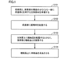
- FIG. 1 is a flowchart showing an outline of the manufacturing method of the present embodiment.
- FIG. 2 is a schematic cross-sectional view illustrating a part of the manufacturing method.
- the manufacturing method includes a step of preparing a support member 20b having an adhesive portion Bp and a stepped portion Sp (S101), and a step of placing the cushioning material 2 on the stepped portion Sp (S102). ), Arranging the seed crystal 10 on the support surface Sf and bonding the bonding portion Bp and the seed crystal 10 (S103), and growing the single crystal 11 on the seed crystal 10 (S104).
- each step will be described.
- Step of preparing support member (S101) In this step, a support member having an adhesive portion Bp and a stepped portion Sp on at least a part of the periphery of the adhesive portion Bp is prepared.
- the support member is made of, for example, graphite, and may function as a lid of the crucible 30 (see FIG. 2).
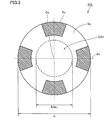
- FIG. 3 is a schematic plan view showing an example of the support member.
- the planar shape of the support member 20 a is circular, and includes an adhesive portion Bp and a stepped portion Sp that recedes lower than the adhesive portion Bp.
- the buffer material 2 is disposed in the stepped portion Sp, so that the bonding portion Bp and the buffer material 2 constitute a support surface Sf (see FIG. 2).
- four stepped portions Sp are provided, but it is sufficient that the stepped portions Sp are provided at least in part, and the number thereof is not particularly limited.
- Figure 3 it illustrates the diameter of the supporting member 20a (i.e. the diameter of the support surface Sf) as d 1.
- the object of this embodiment is to produce a single crystal having a large diameter (for example, a diameter of 150 mm or more).
- the diameter d 1 is preferably 150 mm or more, more preferably 175 mm or more, and particularly preferably 200 mm or more.
- the diameter d 1 may be 300 mm or less.
- the stepped portion Sp is preferably provided outside the center region CR1 including the center point Cp in the plan view of the support member 20a and having a diameter of 0.5d 1 or more. This is because thermal stress generated in the outer peripheral region of the single crystal 11 can be relaxed while securing the area of the bonding portion Bp.
- the diameter of the central region CR1 is more preferably 0.6d 1 or more, 0.7d 1 or more are particularly preferred. This is because by increasing the area of the bonding portion Bp, heat is released from the vicinity of the center of the single crystal 11, and the outer shape of the single crystal 11 can be easily controlled to be convex. If the outer shape of the single crystal 11 can be made convex in the initial stage of growth, it is easy to suppress the mixing of different polytypes.
- the stepped portion Sp is preferably provided symmetrically with respect to the central axis Ax of the support member 20a in accordance with this temperature distribution. This is because the cushioning material 2 is disposed so as to face a portion where thermal stress is likely to occur due to the temperature distribution.
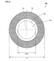
- FIG. 4 is a schematic plan view showing an example of a support member suitable for such a case.
- the stepped portion Sp is provided point-symmetrically with respect to the center point Cp of the support member 20b so as to surround the periphery of the bonding portion Bp. According to the support member 20b, the crystal quality of the single crystal 11 can be improved because it can cope with a concentric temperature distribution.
- the support member may be composed of, for example, two parts.
- FIG. 5 is a schematic cross-sectional view showing an example of a support member composed of two parts.
- the support member 20 c includes a first support member 21 and a second support member 22.
- the second support member 22 is made of, for example, graphite.
- the first support member 21 having the bonding portion Bp is preferably made of a material having a thermal expansion coefficient close to that of the seed crystal 10.
- the first support member 21 can be composed of a SiC single crystal or a SiC polycrystal.
- the first support member 21 may be made of graphite in the same manner as the second support member 22.
- the first support member 21 and the second support member 22 may be joined by, for example, an adhesive or a fitting structure.
- a carbon adhesive is suitable for the adhesive.
- a carbon adhesive is an adhesive formed by dispersing graphite fine particles in an organic solvent. Specific examples include “ST-201” manufactured by Nisshinbo Chemical Co., Ltd.
- Such a carbon adhesive can also be carbonized by heat treatment, whereby the objects can be firmly bonded to each other.
- the carbon adhesive is temporarily held at a temperature of about 150 ° C. or higher and about 300 ° C. or lower to vaporize the organic solvent, and further held at a high temperature of about 500 ° C. or higher and about 1000 ° C. or lower to carbonize the carbon adhesive. be able to.
- the buffer material 2 is disposed on the stepped portion Sp.
- the cushioning material 2 may be adhered to the stepped portion Sp or simply placed.
- the bonding portion Bp and the cushioning material 2 constitute the support surface Sf.
- the cushioning material 2 is preferably arranged symmetrically with respect to the center axis Ax of the support member, more preferably symmetrical with respect to the center point Cp of the support member.
- the thickness of the buffer material 2 is preferably 0.1 mm or greater and 2.0 mm or less. If the thickness is less than 0.1 mm, the effect of relieving thermal stress may be reduced. If the thickness exceeds 2.0 mm, the temperature difference in the thickness direction of the buffer material 2 increases, and the effect of relaxing the thermal stress in the vicinity of the outer periphery in the SiC single crystal may be reduced. In order to efficiently relieve the thermal stress, the thickness of the buffer material 2 is more preferably 0.1 mm or more and 1.0 mm or less, and particularly preferably 0.2 mm or more and 0.8 mm or less. When the buffer material is in the form of a sheet, a plurality of buffer materials may be laminated and used. In this case, the thickness of the buffer material indicates the sum of the thicknesses of the plurality of stacked buffer materials.
- Step of Bonding Bonded Part and Seed Crystal As shown in FIG. 2 or 5, in this step, the bonding portion Bp of the support member and the seed crystal 10 are bonded.
- the above-described carbon adhesive may be used.
- the buffer material 2 that forms the support surface Sf together with the bonding portion Bp and the seed crystal 10 do not necessarily have to be bonded. However, it is desirable that a gap is not generated between the buffer material 2 and the seed crystal 10. If there is a gap between the two, the seed crystal 10 (SiC) is sublimated to the lower temperature side (supporting member side) in the portion, and a fine through hole may be generated in the seed crystal 10. Because.
- an adhesive may be used in the same manner as the bonding part Bp, and the buffer material 2 and the seed crystal 10 may be brought into close contact with each other so that no gap is generated therebetween.
- the seed crystal 10 may be prepared by slicing a SiC ingot (single crystal) such as polytype 4H or 6H to a predetermined thickness. Polytype 4H is particularly useful for devices. What is necessary is just to use a wire saw etc. for a slice, for example.
- the surface (hereinafter also referred to as “growth surface”) on which the single crystal 11 grows among the main surfaces of the seed crystal 10 may be, for example, the (0001) plane (so-called Si plane) side. However, it may be the (000-1) plane (so-called C plane) side.
- the growth surface of the seed crystal 10 is desirably a surface sliced so as to be inclined by 1 ° or more and 10 ° or less from the ⁇ 0001 ⁇ plane. That is, it is desirable that the off angle with respect to the ⁇ 0001 ⁇ plane of the seed crystal 10 is 1 ° or more and 10 ° or less. This is because by limiting the off-angle of the seed crystal 10 in this way, crystal defects such as basal plane dislocations can be suppressed.
- the off-angle is more preferably 1 ° to 8 °, and particularly preferably 2 ° to 8 °.
- the off direction is, for example, the ⁇ 11-20> direction.
- the planar shape of the seed crystal 10 is, for example, a circle.
- the present embodiment suppresses crystal defects that become apparent when a large-diameter SiC single crystal is grown. Therefore, as the SiC single crystal having a large diameter is grown using the seed crystal 10 having a large diameter, the superiority of the present embodiment with respect to the prior art becomes more conspicuous. As will be described later, the present inventor has confirmed the superiority of the present embodiment over the prior art in an experiment using a seed crystal having a diameter of 150 mm. This difference is expected to be even greater when the seed crystal diameter is larger than 150 mm.
- the diameter of the seed crystal 10 is preferably 150 mm or more, more preferably 175 mm or more (for example, 7 inches or more), and particularly preferably 200 mm or more (for example, 8 inches or more).
- the diameter of seed crystal 10 may be 300 mm or less (for example, 12 inches or less).
- the thickness of the seed crystal 10 may be 0.5 mm or more and 5 mm or less, for example.
- the present embodiment may be applied to a thin seed crystal having a thickness of 0.5 mm to 2 mm. This is because the thinner the seed crystal, the easier the distortion.
- the surface of the main surface of the seed crystal 10 to be bonded to the bonding portion Bp (hereinafter also referred to as “bonding surface”) is subjected to a process for increasing the surface roughness. It is preferable. This is to increase the adhesive strength with the support member (bonding part Bp).
- An example of such a process is a polishing process using abrasive grains having a relatively large particle diameter.
- polishing may be performed using a diamond slurry having an average particle size of 5 ⁇ m to 50 ⁇ m (preferably 10 ⁇ m to 30 ⁇ m, more preferably 12 ⁇ m to 25 ⁇ m).
- the “average particle diameter” indicates a median diameter (so-called “D50”) measured by a laser diffraction scattering method.
- the bonding surface may be a pear ground (as sliced surface) formed by slicing and not polished.
- a textured surface has a large surface roughness and may be preferable from the viewpoint of adhesive strength.
- Step of growing single crystal As shown in FIG. 2, in this step, a single crystal 11 is grown on the growth surface of the seed crystal 10.
- FIG. 2 shows an example by the sublimation method.
- the support member 20b is illustrated in FIG. 2, the above-described support member 20a and the support member 20c can also be used.
- the raw material 1 is stored in the bottom of the crucible 30.
- a conventional SiC raw material can be used.
- a powder obtained by pulverizing SiC polycrystal or single crystal can be used.
- the support member 20 b is disposed on the crucible 30 so that the growth surface of the seed crystal 10 faces the raw material 1.
- the support member 20b may function as a lid for the crucible 30 at this time.
- a heat insulating material 31 is disposed around the crucible 30. These are installed in a chamber 33 made of quartz, for example.
- a stainless steel flange 35 is provided at the upper end and lower end of the chamber 33, and a view port 34 is provided on the flange 35.
- a non-contact type thermometer such as a radiation thermometer (pyrometer) is used, the temperature of the bottom or ceiling of the crucible 30 can be measured and monitored through the view port 34.
- the temperature of the bottom portion reflects the temperature of the raw material 1
- the temperature of the ceiling portion reflects the temperatures of the seed crystal 10 and the single crystal 11.
- the temperature environment in the crucible 30 is controlled by the amount of current flowing through the high-frequency coil 32 disposed so as to surround the chamber 33.
- the temperature of the bottom of the crucible 30 is set to, for example, about 2200 ° C. to 2400 ° C.
- the temperature of the ceiling of the crucible 30 is set to, for example, about 2000 ° C. to 2200 ° C.
- Crystal growth is performed in an Ar atmosphere by supplying argon (Ar) gas into the chamber 33. At this time, if an appropriate amount of nitrogen (N 2 ) gas is supplied together with Ar, nitrogen becomes a dopant, and the n-type conductivity can be imparted to the single crystal 11.
- the pressure condition in the chamber 33 is preferably 0.1 kPa or more and atmospheric pressure or less, and more preferably 10 kPa or less from the viewpoint of crystal growth rate.
- the seed crystal 10 is directly bonded to the support member 20b without the buffer material 2 in the bonding portion Bp. Therefore, it is possible to suppress the occurrence of a problem that the seed crystal 10 falls during crystal growth and to realize a crystal growth rate suitable for mass production.
- the present embodiment has been described with reference to the sublimation method.
- the present embodiment is not limited to the sublimation method, and the single crystal is grown on the seed crystal while the seed crystal is fixed to the support member.
- Widely applicable to manufacturing methods for example, in addition to a method of growing a single crystal from the vapor phase, such as a sublimation method such as CVD (Chemical Vapor Deposition) using various source gases, a flux method, a liquid phase epitaxial method, a Bridgman method, a Czochralski method, etc. It can also be applied to a method of growing a single crystal from the liquid phase.
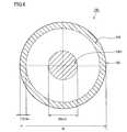
- FIG. 6 is a schematic plan view showing an outline of the SiC substrate according to the present embodiment.
- the SiC substrate 100 is a substrate having a diameter d 2 of 150 mm or more, is formed along the central region CR2 having a diameter of 50 mm and the outer peripheral end OE, and the distance from the outer peripheral end OE is within 10 mm.
- an outer peripheral region OR SiC substrate 100 is typically a slice of single crystal 11 (ingot) obtained by the above-described manufacturing method. Therefore, the crystal plane orientation shift between the center region CR2 and the outer peripheral region OR is small, and the frequency of cracking in the device manufacturing process is extremely low despite the large diameter of 150 mm or more.
- the thickness of the SiC substrate 100 is, for example, about 0.1 mm or more and 0.6 mm or less. From the viewpoint of device raw material costs, the thinner the SiC substrate 100 is, the better. However, the thinner the SiC substrate, the more likely it is to break, thereby reducing the device yield and possibly increasing the device manufacturing cost. In particular, in the case of a large-diameter substrate having a diameter of 150 mm or more, it is necessary to ensure a certain thickness in consideration of substrate handling. Therefore, in the prior art, it has been extremely difficult to realize a SiC substrate having a diameter of 150 mm or more and a thickness of 0.5 mm or less.
- the SiC substrate according to the present embodiment can endure without cracking in the device manufacturing process even at a thickness of 0.4 mm or less as shown in the evaluation described later. Therefore, the thickness of SiC substrate 100 is preferably about 0.5 mm or less, and more preferably about 0.4 mm or less. This may reduce the raw material cost of the device. However, considering the handling of the substrate, the thickness of the SiC substrate 100 is preferably about 0.2 mm or more, and more preferably about 0.3 mm or more. That is, the thickness of the SiC substrate 100 is preferably about 0.2 mm to 0.5 mm, and most preferably about 0.3 mm to 0.4 mm. The diameter of the SiC substrate may be 300 mm or less.
- the deviation of the crystal plane orientation between the center region CR2 and the outer peripheral region OR can be measured by, for example, a two-crystal X-ray diffraction method.
- this measuring method is only an example, and any method may be used as long as it can measure the deviation of crystal plane orientation.
- FIG. 7 is a schematic diagram illustrating an example of a method for measuring the deviation of crystal plane orientation.
- Each “X” -shaped legend written in the SiC substrate 100 indicates a measurement point of crystal plane orientation.
- the measurement point mp1, the measurement point mp2, and the measurement point mp3 belong to the central region CR2, and the measurement point mp4 belongs to the outer peripheral region OR.
- the lower part of FIG. 7 schematically shows the crystal plane orientation at each measurement point.
- the arrows in FIG. 7 indicate X-ray incidence and reflection.
- the crystal plane cf is, for example, a ⁇ 0001 ⁇ plane. In FIG. 7, for example, the crystal plane orientation at the measurement point mp1 is shown as ⁇ 1 (°).
- the crystal plane orientations at the three measurement points belonging to the central region CR2 are averaged to determine the reference orientation ⁇ a.
- the crystal plane orientation ⁇ 4 at the measurement point mp4 belonging to the outer peripheral region OR is measured.
- the shift ⁇ is 200 arcsec or less. From the viewpoint of device yield, the shift ⁇ is more preferably 100 arcsec or less, and particularly preferably 50 arcsec or less. The smaller the shift ⁇ , the better and ideally zero degrees, but the lower limit may be set to about 10 arcsec from the viewpoint of productivity.
- the above measurement is performed by the following procedure, for example. First, a part having the largest lattice plane inclination in the outer peripheral region OR is specified by the X-ray topograph, and then the measurement point mp4 is selected from the part, and the lattice plane inclination ( ⁇ ) is further determined by the two-crystal X-ray diffraction method. taking measurement.
- X-ray rocking curve (XRC) measurement may be performed at the measurement point mp1, the measurement point mp2, the measurement point mp3, and the measurement point mp4.
- the diffractive surface is a (0004) surface.
- the full width at half maximum (FWHM) is measured at each measurement point.
- the measurement conditions are as follows: X-ray source: CuK ⁇ Diffraction angle: 17.85 ° Scanning speed: 0.1 ° / min Sampling interval: 0.002 °.
- Measurement is performed in a 1 mm ⁇ 1 mm area centered on each measurement point.
- the FWHM at the measurement point mp1, the measurement point mp2, and the measurement point mp3 is averaged to obtain an average value at the three points.
- the absolute value of the difference between the average value of the FWHM and the FWHM at the measurement point mp4 is obtained.
- ⁇ FWHM is also an index of deviation between the crystal plane orientation in the central region and the crystal plane orientation in the outer peripheral region.
- ⁇ FWHM is 20 arcsec or less. According to the inventor's research, a substrate with a ⁇ FWHM exceeding 20 arcsec is likely to break during the device manufacturing process. On the other hand, a substrate having ⁇ FWHM of 20 arcsec or less has high resistance to cracking.
- ⁇ FWHM is preferably as small as possible, and ideally 0 arcsec.
- the upper limit of ⁇ FWHM may be 19 arcsec, 18 arcsec, 17 arcsec, or 16 arcsec.
- the lower limit of ⁇ FWHM may be 0 arcsec, 5 arcsec, 10 arcsec, or 15 arcsec.
- a SiC substrate was manufactured under the manufacturing conditions ⁇ , ⁇ , and ⁇ as described below, and the crystal plane orientation shift and the handling in the device manufacturing process (whether or not it can withstand cracking during the manufacturing process) were evaluated.
- the substrate obtained from the manufacturing condition ⁇ is referred to as “substrate ⁇ 1”, for example.
- Step of arranging cushioning material (S102) As shown in FIGS. 2 and 4, the buffer material 2 (graphite sheet with a thickness of 1.0 mm) is arranged on the stepped portion Sp, and the support member 20 b and the buffer material 2 are bonded using a carbon adhesive. did. Thereby, the support surface Sf comprised from the adhesion part Bp and the buffer material 2 was formed.
- Step of Bonding Bonded Part and Seed Crystal A SiC seed crystal 10 having a diameter of 150 mm and a thickness of 1.5 mm was prepared.
- the seed crystal 10 had a crystal structure of polytype 4H, and had a growth surface that was 4 ° off from the (0001) plane.
- the carbon adhesive described above was applied to the adhesion surface of the seed crystal 10 (the surface located on the opposite side of the growth surface) and attached to the support surface Sf.
- the support member 20b on which the seed crystal 10 was affixed was stored for 5 hours in a thermostat set at 200 ° C., and the organic solvent contained in the carbon adhesive was vaporized.
- the support member 20b to which the seed crystal 10 was attached was heat-treated at 750 ° C. for 10 hours to carbonize the carbon adhesive. Thereby, the bonding part Bp and the buffer material 2 and the seed crystal 10 were bonded.
- Step of growing single crystal (S104) As shown in FIG. 2, the raw material 1 which is SiC powder was accommodated in the bottom part of the graphite crucible 30, and the support member 20b in which the seed crystal 10 was attached to the ceiling part of the crucible 30 was arranged. Next, a heat insulating material 31 was placed around the crucible 30 and placed in a quartz chamber 33 of a high-frequency heating device.
- MOSFETs Metal Oxide Semiconductor Field Effect Transistors
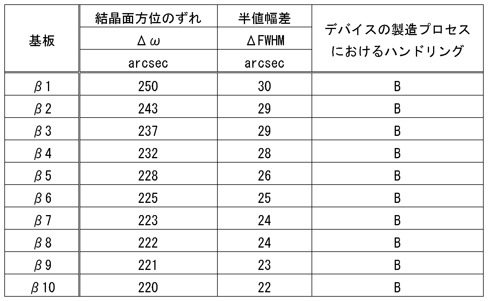
- the crystal plane orientation deviation ⁇ of the substrates ⁇ 1 to ⁇ 10 was measured according to the method described above. The results are shown in Table 2. As shown in Table 2, in the substrates ⁇ 1 to ⁇ 10, the crystal plane orientation was shifted by about 220 to 250 arcsec between the central region and the outer peripheral region.
- ⁇ FWHM was measured on the substrates ⁇ 1 to ⁇ 10 according to the method described above. The results are shown in Table 2. As shown in Table 2, ⁇ FWHM exceeded 20 arcsec for the substrates ⁇ 1 to ⁇ 10.
- MOSFETs were fabricated using the substrates ⁇ 1 to ⁇ 10, and the handling in the device manufacturing process was evaluated based on the above-mentioned two levels. The results are shown in Table 2. As shown in Table 2, in the substrates ⁇ 1 to ⁇ 10, all the substrates were cracked during the manufacturing process, and it was difficult to produce a device.
- the bonding portion Bp and the buffer material 2 constitute a support surface Sf
- the seed crystal 10 is disposed on the support surface Sf and the bonding portion Bp and the seed crystal 10 are bonded
- the SiC single crystal manufacturing method including S103) and the step of growing the single crystal 11 on the seed crystal 10 (S104) is a manufacturing method suitable for mass production of large-diameter substrates.
- the diameter d 2 150 mm or more includes a central region CR2 having a diameter of 50 mm, formed along the outer peripheral end OE, and the outer region OR is the distance from the outer peripheral edge OE is within 10 mm, the
- the crystal plane orientation measured at any three points in the central region CR2 is averaged to be the reference orientation ⁇ a
- the deviation between the crystal plane orientation measured at any point in the outer peripheral region OR and the reference orientation ⁇ a is
- the SiC substrate of 200 arcsec or less is an SiC substrate that can withstand practical use with extremely low frequency of cracking in the device manufacturing process.
Landscapes
- Chemical & Material Sciences (AREA)
- Engineering & Computer Science (AREA)
- Crystallography & Structural Chemistry (AREA)
- Materials Engineering (AREA)
- Metallurgy (AREA)
- Organic Chemistry (AREA)
- Inorganic Chemistry (AREA)
- Crystals, And After-Treatments Of Crystals (AREA)
Abstract
Description
最初に本開示の実施態様を列記して説明する。以下の説明では、同一または対応する要素には同一の符号を付し、それらについて同じ説明は繰り返さない。また本明細書の結晶学的記載においては、個別方位を[]、集合方位を<>、個別面を()、集合面を{}でそれぞれ示す。また結晶学上の指数が負であることは、通常、数字の上に”-”(バー)を付すことによって表現されるが、本明細書では数字の前に負の符号を付すことによって結晶学上の負の指数を表現する。
基板の厚さを0.4mm以下とすることにより、デバイスの製造コストを削減できる可能性がある。また基板の厚さを0.3mm以上とすることにより、デバイスの製造プロセスにおけるハンドリングが容易となる。一般にSiC基板は口径が大きく、薄いほど割れやすい。そのため従来は、直径が150mm以上であり、厚さが0.5mm以下である基板の実現は極めて困難であった。しかし上記〔8〕の如く、結晶面方位のずれが200arcsec以下であれば、大口径で、なおかつ厚さの薄い基板であっても、デバイスの製造プロセスにおいて割れずに耐えることができる。
以下、本開示の実施形態(以下「本実施形態」とも記す)について詳細に説明するが、本実施形態はこれらに限定されるものではない。
図1は、本実施形態の製造方法の概略を示すフローチャートである。図2は、当該製造方法の一部を図解する模式的な断面図である。図1および図2に示すように、当該製造方法は、接着部Bpと段差部Spとを有する支持部材20bを準備する工程(S101)と、段差部Spに緩衝材2を配置する工程(S102)と、支持面Sf上に種結晶10を配置するとともに接着部Bpと種結晶10とを接着する工程(S103)と、種結晶10上に単結晶11を成長させる工程(S104)と、を備える。以下、各工程について説明する。
この工程では、接着部Bpと、接着部Bpの周縁の少なくとも一部に段差部Spとを有する支持部材を準備する。支持部材は、たとえば黒鉛製であり、坩堝30(図2参照)の蓋として機能させてもよい。
この工程では段差部Spに緩衝材2を配置する。緩衝材2は段差部Spに接着してもよいし、単に載せ置くだけでもよい。図2に示すように、段差部Spに緩衝材2が配置されることにより、接着部Bpと緩衝材2とが支持面Sfを構成することになる。前述のように緩衝材2は、好ましくは支持部材の中心軸Axに対して軸対称、より好ましくは支持部材の中心点Cpに対して点対称に配置される。
緩衝材2には、たとえば黒鉛シート等の耐熱性を有しかつ柔軟性に富む素材が好適である。緩衝材2の厚さは0.1mm以上2.0mm以下が好ましい。厚さが0.1mmよりも薄いと熱応力を緩和する効果が低減する可能性がある。また厚さが2.0mmを超えると緩衝材2の厚さ方向での温度差が大きくなって、SiC単結晶において外周近傍の熱応力を緩和する効果が低減する可能性もある。熱応力を効率的に緩和するためには、緩衝材2の厚さは0.1mm以上1.0mm以下がより好ましく、0.2mm以上0.8mm以下が特に好ましい。緩衝材がシート状である場合、複数の緩衝材を積層して使用してもよい。その場合、緩衝材の厚さとは、積層された複数の緩衝材の厚さの総和を示すものとする。
図2または図5に示すように、この工程では支持部材の接着部Bpと種結晶10とを接着する。接着には、たとえば前述のカーボン接着剤を使用すればよい。接着部Bpとともに支持面Sfを構成する緩衝材2と、種結晶10とは必ずしも接着しなくてもよい。ただし、緩衝材2と種結晶10との間には隙間が生じない態様とすることが望ましい。両者の間に隙間が存在すると、当該部分において種結晶10(SiC)が温度の低い側(支持部材側)へと昇華してしまい、種結晶10に微細な貫通孔が発生する可能性があるからである。たとえば接着部Bpと同様に接着剤を使用して、緩衝材2と種結晶10とをその間に隙間が生じないように密着させるとよい。
種結晶10は、たとえばポリタイプ4H、6H等のSiCインゴット(単結晶)を所定の厚さにスライスして準備すればよい。ポリタイプ4Hはデバイス用として特に有用である。スライスには、たとえばワイヤーソー等を使用すればよい。図2に示すように、種結晶10の主面のうち単結晶11が成長することになる面(以下「成長面」とも記す)は、たとえば(0001)面〔いわゆるSi面〕側としてもよいし、(000-1)面〔いわゆるC面〕側としてもよい。
図2に示すように、この工程では、種結晶10の成長面上に単結晶11を成長させる。図2では昇華法による例を図示している。図2には支持部材20bを図示しているが、前述の支持部材20aおよび支持部材20cも当然使用できる。
次に本実施形態に係るSiC基板について説明する。図6は本実施形態に係るSiC基板の概略を示す模式的な平面図である。図6に示すように、SiC基板100は直径d2が150mm以上の基板であり、直径が50mmである中心領域CR2と、外周端OEに沿って形成され、外周端OEからの距離が10mm以内である外周領域ORと、を備えている。SiC基板100は、典型的には前述の製造方法によって得られた単結晶11(インゴット)をスライスしたものである。したがって中心領域CR2と外周領域ORとの間での結晶面方位のずれが小さく、直径150mm以上の大口径であるにもかかわらず、デバイスの製造プロセスにおいて割れる頻度が極めて低い。
中心領域CR2と外周領域ORとの間での結晶面方位のずれは、たとえば2結晶X線回折法によって測定することができる。ただしこの測定方法は一例に過ぎず、結晶面方位のずれを測定できる方法であれば如何なる方法を使用しても構わない。
ωa=(ω1+ω2+ω3)÷3・・・式(1)
から算出できる。このとき3つの測定点mp1、mp2およびmp3の選択は任意であるが、各測定点間の距離が等間隔となるように選択することが望ましい。
Δω=|ω4-ωa|・・・式(2)
によって算出できる。本実施形態では、ずれΔωは200arcsec以下となる。デバイスの歩留まりの観点から、ずれΔωは100arcsec以下がより好ましく、50arcsec以下が特に好ましい。ずれΔωは小さいほど望ましく理想的にはゼロ度であるが、生産性の観点からその下限値は10arcsec程度に設定してもよい。
X線源:CuKα
回折角:17.85°
走査速度:0.1°/分
サンプリング間隔:0.002°。
以下のように製造条件α、βおよびγによってSiC基板を製造し、さらに結晶面方位のずれ、およびデバイスの製造プロセスにおけるハンドリング(製造プロセス中、割れずに耐え得るか否か)を評価した。以下の説明では製造条件αから得られた基板は、たとえば「基板α1」と記すものとする。
〔支持部材を準備する工程(S101)〕
図2および図4に示すように、平面形状が円形である黒鉛製の支持部材20bを準備した。このとき支持部材20bの直径d1は150mmとし、中心点Cpを含み直径が75mmである中心領域CR1(接着部Bp)の外側に、接着部Bpよりも1.05mm低く後退した段差部Spを形成した。
図2および図4に示すように、段差部Spに、緩衝材2(厚さ1.0mmの黒鉛シート)を配置し、さらにカーボン接着剤を使用して支持部材20bと緩衝材2とを接着した。これにより接着部Bpと緩衝材2とから構成される支持面Sfが形成された。
直径150mm、厚さ1.5mmのSiC種結晶10を準備した。種結晶10はポリタイプ4Hの結晶構造を有し、(0001)面から4°オフされた成長面を有するものであった。種結晶10の接着面(成長面の反対側に位置する面)に前述のカーボン接着剤を塗布し、支持面Sfに貼り付けた。次いで種結晶10が貼り付けられた支持部材20bを200℃に設定された恒温槽内で5時間保管して、カーボン接着剤に含まれる有機溶剤を気化させた。その後、高温炉を使用し、種結晶10が貼り付けられた支持部材20bを750℃で10時間に亘って熱処理して、カーボン接着剤を炭化させた。これにより接着部Bpおよび緩衝材2と種結晶10とを接着した。
図2に示すように、黒鉛製の坩堝30の底部にSiC粉末である原料1を収容し、坩堝30の天井部に種結晶10が貼り付けられた支持部材20bを配置した。次いで坩堝30の周囲に断熱材31を配置し、それらを高周波式加熱装置の石英製チャンバー33内に設置した。
単結晶11の側面を研削した後、ワイヤーソーでスライスして10枚の基板を得た。さらに各基板のスライス面を鏡面研磨して、厚さ350μm、直径150mmのミラーウェーハである基板α1~α10を得た。
基板α1~α10の結晶面方位のずれΔωを前述の方法に従って測定した。結果を表1に示す。表1に示すように、基板α1~α10におけるΔωは、いずれも200arcsec以下であった。
基板α1~α10において、ΔFWHMを前述の方法に従って測定した。結果を表1に示す。表1に示すように、基板α1~α10におけるΔFWHMは、いずれも20arcsec以下であった。

基板α1~α10を使用して、MOSFET(Metal Oxide Semiconductor Field Effect Transistor)を作製し、デバイスの製造プロセスにおけるハンドリングを以下の「A」および「B」の2水準で評価した。結果を表1に示す。表1に示すように基板α1~α10では割れが生じておらず、いずれもハンドリングは良好であった。
B:基板に割れが生じた。
製造条件βでは従来技術の如く、段差部を有さない支持部材を使用した。前述の種結晶10の接着面にカーボン接着剤を塗布し、接着面の全面をこの支持部材に貼り付けた。これ以外の条件は製造条件αと同様にして単結晶11を成長させ、さらに基板β1~β10を得た。
製造条件γでは、カーボン接着剤を使用して種結晶10の接着面の全面に前述の黒鉛シートを貼り付けた後、該黒鉛シートを挟んで種結晶10と支持部材20bとを接着することを除いては、製造条件αと同様にして単結晶11を成長させた。
第一に、接着部Bpと、接着部Bpの周縁の少なくとも一部に段差部Spとを有する支持部材20bを準備する工程(S101)と、段差部Spに緩衝材2を配置する工程(S102)と、を備え、接着部Bpと緩衝材2とは支持面Sfを構成し、さらに、支持面Sf上に種結晶10を配置するとともに、接着部Bpと種結晶10とを接着する工程(S103)と、種結晶10上に単結晶11を成長させる工程(S104)と、を備えるSiC単結晶の製造方法は、大口径基板の量産に相応しい製造方法である。
Claims (10)
- 接着部と、前記接着部の周縁の少なくとも一部に段差部とを有する支持部材を準備する工程と、
前記段差部に緩衝材を配置する工程と、を備え、
前記接着部と前記緩衝材とは支持面を構成し、さらに、
前記支持面上に種結晶を配置するとともに、前記接着部と前記種結晶とを接着する工程と、
前記種結晶上に単結晶を成長させる工程と、を備える、炭化珪素単結晶の製造方法。 - 前記支持面の平面形状は円形であり、
前記支持面の直径をd1とするとき、前記段差部は、前記支持面の中心点を含みかつ直径が0.5d1以上である中心領域の外側に位置する、請求項1に記載の炭化珪素単結晶の製造方法。 - 前記配置する工程において、
前記緩衝材は、前記支持部材の中心軸に対して軸対称に配置される、請求項1または請求項2に記載の炭化珪素単結晶の製造方法。 - 前記配置する工程において、
前記緩衝材は、前記支持部材の中心点に対して点対称に配置される、請求項1に記載の炭化珪素単結晶の製造方法。 - 前記支持部材は、前記接着部を有する第1の支持部材と、前記第1の支持部材と接合する第2の支持部材とを含み、
前記第1の支持部材と前記第2の支持部材とが接合する部分の周縁の少なくとも一部に前記段差部を有する、請求項1~請求項4のいずれか1項に記載の炭化珪素単結晶の製造方法。 - 前記緩衝材の厚さは、0.1mm以上2.0mm以下である、請求項1~請求項5のいずれか1項に記載の炭化珪素単結晶の製造方法。
- 前記種結晶の直径は、150mm以上である、請求項1~請求項6のいずれか1項に記載の炭化珪素単結晶の製造方法。
- 直径が150mm以上であり、
直径が50mmである中心領域と、
外周端に沿って形成され、前記外周端からの距離が10mm以内である外周領域と、を備え、
前記中心領域内の任意の3点で測定した結晶面方位を平均して基準方位としたとき、前記外周領域内の任意の点で測定される結晶面方位と前記基準方位とのずれが200arcsec以下である、炭化珪素基板。 - 厚さが0.3mm以上0.4mm以下である、請求項8に記載の炭化珪素基板。
- 前記中心領域内の任意の3点で測定した(0004)面のX線ロッキングカーブの半値全幅の平均値と、前記外周領域内の任意の点で測定される(0004)面のX線ロッキングカーブの半値全幅との差の絶対値が、20arcsec以下である、請求項8または請求項9に記載の炭化珪素基板。
Priority Applications (4)
| Application Number | Priority Date | Filing Date | Title |
|---|---|---|---|
| US15/319,107 US20170121844A1 (en) | 2014-07-07 | 2015-06-24 | Method for manufacturing silicon carbide single crystal and silicon carbide substrate |
| DE112015003168.5T DE112015003168T5 (de) | 2014-07-07 | 2015-06-24 | Verfahren zur Herstellung eines Siliziumkarbid-Einkristalls und Siliziumkarbid-Substrat |
| JP2016532862A JPWO2016006442A1 (ja) | 2014-07-07 | 2015-06-24 | 炭化珪素単結晶の製造方法および炭化珪素基板 |
| CN201580035227.2A CN106471165A (zh) | 2014-07-07 | 2015-06-24 | 碳化硅单晶的制造方法和碳化硅基板 |
Applications Claiming Priority (2)
| Application Number | Priority Date | Filing Date | Title |
|---|---|---|---|
| JP2014-139432 | 2014-07-07 | ||
| JP2014139432 | 2014-07-07 |
Publications (1)
| Publication Number | Publication Date |
|---|---|
| WO2016006442A1 true WO2016006442A1 (ja) | 2016-01-14 |
Family
ID=55064080
Family Applications (1)
| Application Number | Title | Priority Date | Filing Date |
|---|---|---|---|
| PCT/JP2015/068162 Ceased WO2016006442A1 (ja) | 2014-07-07 | 2015-06-24 | 炭化珪素単結晶の製造方法および炭化珪素基板 |
Country Status (5)
| Country | Link |
|---|---|
| US (1) | US20170121844A1 (ja) |
| JP (1) | JPWO2016006442A1 (ja) |
| CN (1) | CN106471165A (ja) |
| DE (2) | DE202015009519U1 (ja) |
| WO (1) | WO2016006442A1 (ja) |
Cited By (3)
| Publication number | Priority date | Publication date | Assignee | Title |
|---|---|---|---|---|
| JP2018165227A (ja) * | 2017-03-28 | 2018-10-25 | 昭和電工株式会社 | 炭化珪素単結晶インゴットの製造方法 |
| CN110088363A (zh) * | 2016-12-26 | 2019-08-02 | 昭和电工株式会社 | SiC锭的制造方法 |
| KR20210050835A (ko) * | 2019-10-29 | 2021-05-10 | 에스케이씨 주식회사 | 탄화규소 웨이퍼 및 탄화규소 웨이퍼의 제조방법 |
Families Citing this family (3)
| Publication number | Priority date | Publication date | Assignee | Title |
|---|---|---|---|---|
| KR102068933B1 (ko) * | 2019-07-11 | 2020-01-21 | 에스케이씨 주식회사 | 탄화규소 잉곳 성장용 분말 및 이를 이용한 탄화규소 잉곳의 제조방법 |
| AT524251B1 (de) * | 2020-09-28 | 2023-04-15 | Ebner Ind Ofenbau | Vorrichtung zum Züchten von Einkristallen |
| CN114395803B (zh) * | 2022-01-13 | 2023-08-22 | 浙江大学 | 一种减少碳化硅籽晶背向升华的粘接结构与粘接方法 |
Citations (4)
| Publication number | Priority date | Publication date | Assignee | Title |
|---|---|---|---|---|
| JP2004269297A (ja) * | 2003-03-06 | 2004-09-30 | Toyota Central Res & Dev Lab Inc | SiC単結晶及びその製造方法 |
| JP2010280547A (ja) * | 2009-06-05 | 2010-12-16 | Bridgestone Corp | 炭化珪素単結晶の製造方法 |
| JP2011190129A (ja) * | 2010-03-12 | 2011-09-29 | Bridgestone Corp | 炭化ケイ素単結晶の製造装置 |
| JP2011207691A (ja) * | 2010-03-30 | 2011-10-20 | Denso Corp | 炭化珪素単結晶の製造装置および炭化珪素単結晶の製造方法 |
Family Cites Families (1)
| Publication number | Priority date | Publication date | Assignee | Title |
|---|---|---|---|---|
| JP4321107B2 (ja) | 2003-05-13 | 2009-08-26 | 株式会社デンソー | SiC単結晶の製造装置 |
-
2015
- 2015-06-24 CN CN201580035227.2A patent/CN106471165A/zh not_active Withdrawn
- 2015-06-24 DE DE202015009519.4U patent/DE202015009519U1/de not_active Expired - Lifetime
- 2015-06-24 DE DE112015003168.5T patent/DE112015003168T5/de not_active Withdrawn
- 2015-06-24 JP JP2016532862A patent/JPWO2016006442A1/ja active Pending
- 2015-06-24 WO PCT/JP2015/068162 patent/WO2016006442A1/ja not_active Ceased
- 2015-06-24 US US15/319,107 patent/US20170121844A1/en not_active Abandoned
Patent Citations (4)
| Publication number | Priority date | Publication date | Assignee | Title |
|---|---|---|---|---|
| JP2004269297A (ja) * | 2003-03-06 | 2004-09-30 | Toyota Central Res & Dev Lab Inc | SiC単結晶及びその製造方法 |
| JP2010280547A (ja) * | 2009-06-05 | 2010-12-16 | Bridgestone Corp | 炭化珪素単結晶の製造方法 |
| JP2011190129A (ja) * | 2010-03-12 | 2011-09-29 | Bridgestone Corp | 炭化ケイ素単結晶の製造装置 |
| JP2011207691A (ja) * | 2010-03-30 | 2011-10-20 | Denso Corp | 炭化珪素単結晶の製造装置および炭化珪素単結晶の製造方法 |
Cited By (7)
| Publication number | Priority date | Publication date | Assignee | Title |
|---|---|---|---|---|
| CN110088363A (zh) * | 2016-12-26 | 2019-08-02 | 昭和电工株式会社 | SiC锭的制造方法 |
| US11008670B2 (en) | 2016-12-26 | 2021-05-18 | Showa Denko K.K. | Manufacturing method of SiC ingot |
| CN110088363B (zh) * | 2016-12-26 | 2021-06-22 | 昭和电工株式会社 | SiC锭的制造方法 |
| JP2018165227A (ja) * | 2017-03-28 | 2018-10-25 | 昭和電工株式会社 | 炭化珪素単結晶インゴットの製造方法 |
| KR20210050835A (ko) * | 2019-10-29 | 2021-05-10 | 에스케이씨 주식회사 | 탄화규소 웨이퍼 및 탄화규소 웨이퍼의 제조방법 |
| KR102284879B1 (ko) | 2019-10-29 | 2021-07-30 | 에스케이씨 주식회사 | 탄화규소 웨이퍼 및 탄화규소 웨이퍼의 제조방법 |
| US11708644B2 (en) | 2019-10-29 | 2023-07-25 | Senic Inc. | Method for preparing SiC ingot, method for preparing SiC wafer and the SiC wafer prepared therefrom |
Also Published As
| Publication number | Publication date |
|---|---|
| US20170121844A1 (en) | 2017-05-04 |
| CN106471165A (zh) | 2017-03-01 |
| JPWO2016006442A1 (ja) | 2017-04-27 |
| DE202015009519U1 (de) | 2018-02-08 |
| DE112015003168T5 (de) | 2017-03-23 |
Similar Documents
| Publication | Publication Date | Title |
|---|---|---|
| JP5304712B2 (ja) | 炭化珪素単結晶ウェハ | |
| CN110541199B (zh) | 一种直径8英寸及以上尺寸高质量SiC籽晶的制备方法 | |
| JP7464265B2 (ja) | 炭化珪素ウエハ、炭化珪素インゴットの製造方法及び炭化珪素ウエハの製造方法 | |
| CN103620095B (zh) | 碳化硅单晶基板及其制造方法 | |
| TWI750628B (zh) | 碳化矽晶圓以及碳化矽晶圓之製備方法 | |
| JPWO2016006442A1 (ja) | 炭化珪素単結晶の製造方法および炭化珪素基板 | |
| JP4985625B2 (ja) | 炭化珪素単結晶の製造方法 | |
| WO2015182246A1 (ja) | 炭化珪素インゴットの製造方法、炭化珪素種基板および炭化珪素基板 | |
| JP7161784B2 (ja) | 炭化珪素インゴット、ウエハ及びその製造方法 | |
| TW202117100A (zh) | 碳化矽錠之製備方法、碳化矽晶圓之製備方法以及其系統 | |
| TWI837924B (zh) | 碳化矽晶圓製造方法以及碳化矽錠製造方法 | |
| JP6120742B2 (ja) | 単結晶インゴットの製造方法、単結晶基板の製造方法、および半導体装置の製造方法 | |
| US20110217224A1 (en) | Silicon carbide crystal, method of manufacturing the same, apparatus for manufacturing the same, and crucible | |
| JP2020132438A (ja) | 炭化珪素単結晶の製造方法 | |
| JP4494856B2 (ja) | 炭化珪素単結晶成長用種結晶とその製造方法及びそれを用いた結晶成長方法 | |
| JP5761264B2 (ja) | SiC基板の製造方法 | |
| TWI839934B (zh) | 碳化矽晶圓以及其製造方法 | |
| CN115917059A (zh) | 制造碳化硅锭的方法、碳化硅锭及其生长系统 | |
| JP2011051861A (ja) | AlN単結晶の製造方法および種基板 | |
| JP2005093519A (ja) | 炭化珪素基板の製造方法および炭化珪素基板 | |
| CN113322520A (zh) | 晶片及其制造方法 | |
| JP5549722B2 (ja) | 結晶製造方法 | |
| KR102236397B1 (ko) | 탄화규소 웨이퍼 및 이를 적용한 반도체 소자 | |
| JP2015093823A (ja) | 炭化珪素種基板、炭化珪素インゴットの製造方法および炭化珪素単結晶基板 | |
| TW202517843A (zh) | 製造碳化矽錠的方法 |
Legal Events
| Date | Code | Title | Description |
|---|---|---|---|
| 121 | Ep: the epo has been informed by wipo that ep was designated in this application |
Ref document number: 15818490 Country of ref document: EP Kind code of ref document: A1 |
|
| ENP | Entry into the national phase |
Ref document number: 2016532862 Country of ref document: JP Kind code of ref document: A |
|
| WWE | Wipo information: entry into national phase |
Ref document number: 15319107 Country of ref document: US |
|
| WWE | Wipo information: entry into national phase |
Ref document number: 112015003168 Country of ref document: DE |
|
| 122 | Ep: pct application non-entry in european phase |
Ref document number: 15818490 Country of ref document: EP Kind code of ref document: A1 |