WO2016002508A1 - 半導体集積回路装置 - Google Patents
半導体集積回路装置 Download PDFInfo
- Publication number
- WO2016002508A1 WO2016002508A1 PCT/JP2015/067370 JP2015067370W WO2016002508A1 WO 2016002508 A1 WO2016002508 A1 WO 2016002508A1 JP 2015067370 W JP2015067370 W JP 2015067370W WO 2016002508 A1 WO2016002508 A1 WO 2016002508A1
- Authority
- WO
- WIPO (PCT)
- Prior art keywords
- region
- type well
- potential
- well region
- conductivity type
- Prior art date
- Legal status (The legal status is an assumption and is not a legal conclusion. Google has not performed a legal analysis and makes no representation as to the accuracy of the status listed.)
- Ceased
Links
Images







Classifications
-
- H—ELECTRICITY
- H03—ELECTRONIC CIRCUITRY
- H03K—PULSE TECHNIQUE
- H03K19/00—Logic circuits, i.e. having at least two inputs acting on one output; Inverting circuits
- H03K19/0175—Coupling arrangements; Interface arrangements
- H03K19/0185—Coupling arrangements; Interface arrangements using field effect transistors only
- H03K19/018507—Interface arrangements
- H03K19/018521—Interface arrangements of complementary type, e.g. CMOS
-
- H—ELECTRICITY
- H03—ELECTRONIC CIRCUITRY
- H03K—PULSE TECHNIQUE
- H03K17/00—Electronic switching or gating, i.e. not by contact-making and –breaking
- H03K17/51—Electronic switching or gating, i.e. not by contact-making and –breaking characterised by the components used
- H03K17/56—Electronic switching or gating, i.e. not by contact-making and –breaking characterised by the components used by the use, as active elements, of semiconductor devices
- H03K17/567—Circuits characterised by the use of more than one type of semiconductor device, e.g. BIMOS, composite devices such as IGBT
-
- H—ELECTRICITY
- H10—SEMICONDUCTOR DEVICES; ELECTRIC SOLID-STATE DEVICES NOT OTHERWISE PROVIDED FOR
- H10D—INORGANIC ELECTRIC SEMICONDUCTOR DEVICES
- H10D62/00—Semiconductor bodies, or regions thereof, of devices having potential barriers
- H10D62/10—Shapes, relative sizes or dispositions of the regions of the semiconductor bodies; Shapes of the semiconductor bodies
- H10D62/113—Isolations within a component, i.e. internal isolations
- H10D62/115—Dielectric isolations, e.g. air gaps
-
- H—ELECTRICITY
- H10—SEMICONDUCTOR DEVICES; ELECTRIC SOLID-STATE DEVICES NOT OTHERWISE PROVIDED FOR
- H10D—INORGANIC ELECTRIC SEMICONDUCTOR DEVICES
- H10D62/00—Semiconductor bodies, or regions thereof, of devices having potential barriers
- H10D62/10—Shapes, relative sizes or dispositions of the regions of the semiconductor bodies; Shapes of the semiconductor bodies
- H10D62/17—Semiconductor regions connected to electrodes not carrying current to be rectified, amplified or switched, e.g. channel regions
- H10D62/393—Body regions of DMOS transistors or IGBTs
-
- H—ELECTRICITY
- H10—SEMICONDUCTOR DEVICES; ELECTRIC SOLID-STATE DEVICES NOT OTHERWISE PROVIDED FOR
- H10D—INORGANIC ELECTRIC SEMICONDUCTOR DEVICES
- H10D84/00—Integrated devices formed in or on semiconductor substrates that comprise only semiconducting layers, e.g. on Si wafers or on GaAs-on-Si wafers
- H10D84/01—Manufacture or treatment
- H10D84/0123—Integrating together multiple components covered by H10D12/00 or H10D30/00, e.g. integrating multiple IGBTs
- H10D84/0126—Integrating together multiple components covered by H10D12/00 or H10D30/00, e.g. integrating multiple IGBTs the components including insulated gates, e.g. IGFETs
- H10D84/0165—Integrating together multiple components covered by H10D12/00 or H10D30/00, e.g. integrating multiple IGBTs the components including insulated gates, e.g. IGFETs the components including complementary IGFETs, e.g. CMOS devices
- H10D84/0191—Manufacturing their doped wells
-
- H—ELECTRICITY
- H10—SEMICONDUCTOR DEVICES; ELECTRIC SOLID-STATE DEVICES NOT OTHERWISE PROVIDED FOR
- H10D—INORGANIC ELECTRIC SEMICONDUCTOR DEVICES
- H10D84/00—Integrated devices formed in or on semiconductor substrates that comprise only semiconducting layers, e.g. on Si wafers or on GaAs-on-Si wafers
- H10D84/01—Manufacture or treatment
- H10D84/02—Manufacture or treatment characterised by using material-based technologies
- H10D84/03—Manufacture or treatment characterised by using material-based technologies using Group IV technology, e.g. silicon technology or silicon-carbide [SiC] technology
- H10D84/038—Manufacture or treatment characterised by using material-based technologies using Group IV technology, e.g. silicon technology or silicon-carbide [SiC] technology using silicon technology, e.g. SiGe
-
- H—ELECTRICITY
- H10—SEMICONDUCTOR DEVICES; ELECTRIC SOLID-STATE DEVICES NOT OTHERWISE PROVIDED FOR
- H10D—INORGANIC ELECTRIC SEMICONDUCTOR DEVICES
- H10D84/00—Integrated devices formed in or on semiconductor substrates that comprise only semiconducting layers, e.g. on Si wafers or on GaAs-on-Si wafers
- H10D84/60—Integrated devices formed in or on semiconductor substrates that comprise only semiconducting layers, e.g. on Si wafers or on GaAs-on-Si wafers characterised by the integration of at least one component covered by groups H10D10/00 or H10D18/00, e.g. integration of BJTs
- H10D84/645—Combinations of only lateral BJTs
-
- H—ELECTRICITY
- H10—SEMICONDUCTOR DEVICES; ELECTRIC SOLID-STATE DEVICES NOT OTHERWISE PROVIDED FOR
- H10D—INORGANIC ELECTRIC SEMICONDUCTOR DEVICES
- H10D84/00—Integrated devices formed in or on semiconductor substrates that comprise only semiconducting layers, e.g. on Si wafers or on GaAs-on-Si wafers
- H10D84/80—Integrated devices formed in or on semiconductor substrates that comprise only semiconducting layers, e.g. on Si wafers or on GaAs-on-Si wafers characterised by the integration of at least one component covered by groups H10D12/00 or H10D30/00, e.g. integration of IGFETs
- H10D84/82—Integrated devices formed in or on semiconductor substrates that comprise only semiconducting layers, e.g. on Si wafers or on GaAs-on-Si wafers characterised by the integration of at least one component covered by groups H10D12/00 or H10D30/00, e.g. integration of IGFETs of only field-effect components
- H10D84/83—Integrated devices formed in or on semiconductor substrates that comprise only semiconducting layers, e.g. on Si wafers or on GaAs-on-Si wafers characterised by the integration of at least one component covered by groups H10D12/00 or H10D30/00, e.g. integration of IGFETs of only field-effect components of only insulated-gate FETs [IGFET]
- H10D84/85—Complementary IGFETs, e.g. CMOS
-
- H—ELECTRICITY
- H10—SEMICONDUCTOR DEVICES; ELECTRIC SOLID-STATE DEVICES NOT OTHERWISE PROVIDED FOR
- H10W—GENERIC PACKAGES, INTERCONNECTIONS, CONNECTORS OR OTHER CONSTRUCTIONAL DETAILS OF DEVICES COVERED BY CLASS H10
- H10W10/00—Isolation regions in semiconductor bodies between components of integrated devices
-
- H—ELECTRICITY
- H10—SEMICONDUCTOR DEVICES; ELECTRIC SOLID-STATE DEVICES NOT OTHERWISE PROVIDED FOR
- H10W—GENERIC PACKAGES, INTERCONNECTIONS, CONNECTORS OR OTHER CONSTRUCTIONAL DETAILS OF DEVICES COVERED BY CLASS H10
- H10W10/00—Isolation regions in semiconductor bodies between components of integrated devices
- H10W10/01—Manufacture or treatment
-
- H—ELECTRICITY
- H10—SEMICONDUCTOR DEVICES; ELECTRIC SOLID-STATE DEVICES NOT OTHERWISE PROVIDED FOR
- H10W—GENERIC PACKAGES, INTERCONNECTIONS, CONNECTORS OR OTHER CONSTRUCTIONAL DETAILS OF DEVICES COVERED BY CLASS H10
- H10W10/00—Isolation regions in semiconductor bodies between components of integrated devices
- H10W10/01—Manufacture or treatment
- H10W10/011—Manufacture or treatment of isolation regions comprising dielectric materials
- H10W10/014—Manufacture or treatment of isolation regions comprising dielectric materials using trench refilling with dielectric materials, e.g. shallow trench isolations
-
- H—ELECTRICITY
- H10—SEMICONDUCTOR DEVICES; ELECTRIC SOLID-STATE DEVICES NOT OTHERWISE PROVIDED FOR
- H10W—GENERIC PACKAGES, INTERCONNECTIONS, CONNECTORS OR OTHER CONSTRUCTIONAL DETAILS OF DEVICES COVERED BY CLASS H10
- H10W10/00—Isolation regions in semiconductor bodies between components of integrated devices
- H10W10/01—Manufacture or treatment
- H10W10/031—Manufacture or treatment of isolation regions comprising PN junctions
-
- H—ELECTRICITY
- H10—SEMICONDUCTOR DEVICES; ELECTRIC SOLID-STATE DEVICES NOT OTHERWISE PROVIDED FOR
- H10W—GENERIC PACKAGES, INTERCONNECTIONS, CONNECTORS OR OTHER CONSTRUCTIONAL DETAILS OF DEVICES COVERED BY CLASS H10
- H10W10/00—Isolation regions in semiconductor bodies between components of integrated devices
- H10W10/10—Isolation regions comprising dielectric materials
- H10W10/17—Isolation regions comprising dielectric materials formed using trench refilling with dielectric materials, e.g. shallow trench isolations
-
- H—ELECTRICITY
- H10—SEMICONDUCTOR DEVICES; ELECTRIC SOLID-STATE DEVICES NOT OTHERWISE PROVIDED FOR
- H10W—GENERIC PACKAGES, INTERCONNECTIONS, CONNECTORS OR OTHER CONSTRUCTIONAL DETAILS OF DEVICES COVERED BY CLASS H10
- H10W10/00—Isolation regions in semiconductor bodies between components of integrated devices
- H10W10/30—Isolation regions comprising PN junctions
-
- H—ELECTRICITY
- H02—GENERATION; CONVERSION OR DISTRIBUTION OF ELECTRIC POWER
- H02M—APPARATUS FOR CONVERSION BETWEEN AC AND AC, BETWEEN AC AND DC, OR BETWEEN DC AND DC, AND FOR USE WITH MAINS OR SIMILAR POWER SUPPLY SYSTEMS; CONVERSION OF DC OR AC INPUT POWER INTO SURGE OUTPUT POWER; CONTROL OR REGULATION THEREOF
- H02M7/00—Conversion of AC power input into DC power output; Conversion of DC power input into AC power output
- H02M7/003—Constructional details, e.g. physical layout, assembly, wiring or busbar connections
-
- H—ELECTRICITY
- H10—SEMICONDUCTOR DEVICES; ELECTRIC SOLID-STATE DEVICES NOT OTHERWISE PROVIDED FOR
- H10D—INORGANIC ELECTRIC SEMICONDUCTOR DEVICES
- H10D12/00—Bipolar devices controlled by the field effect, e.g. insulated-gate bipolar transistors [IGBT]
- H10D12/411—Insulated-gate bipolar transistors [IGBT]
-
- H—ELECTRICITY
- H10—SEMICONDUCTOR DEVICES; ELECTRIC SOLID-STATE DEVICES NOT OTHERWISE PROVIDED FOR
- H10D—INORGANIC ELECTRIC SEMICONDUCTOR DEVICES
- H10D8/00—Diodes
-
- H—ELECTRICITY
- H10—SEMICONDUCTOR DEVICES; ELECTRIC SOLID-STATE DEVICES NOT OTHERWISE PROVIDED FOR
- H10D—INORGANIC ELECTRIC SEMICONDUCTOR DEVICES
- H10D84/00—Integrated devices formed in or on semiconductor substrates that comprise only semiconducting layers, e.g. on Si wafers or on GaAs-on-Si wafers
- H10D84/80—Integrated devices formed in or on semiconductor substrates that comprise only semiconducting layers, e.g. on Si wafers or on GaAs-on-Si wafers characterised by the integration of at least one component covered by groups H10D12/00 or H10D30/00, e.g. integration of IGFETs
- H10D84/82—Integrated devices formed in or on semiconductor substrates that comprise only semiconducting layers, e.g. on Si wafers or on GaAs-on-Si wafers characterised by the integration of at least one component covered by groups H10D12/00 or H10D30/00, e.g. integration of IGFETs of only field-effect components
- H10D84/83—Integrated devices formed in or on semiconductor substrates that comprise only semiconducting layers, e.g. on Si wafers or on GaAs-on-Si wafers characterised by the integration of at least one component covered by groups H10D12/00 or H10D30/00, e.g. integration of IGFETs of only field-effect components of only insulated-gate FETs [IGFET]
- H10D84/85—Complementary IGFETs, e.g. CMOS
- H10D84/856—Complementary IGFETs, e.g. CMOS the complementary IGFETs having different architectures than each other, e.g. high-voltage and low-voltage CMOS
Definitions
- the present invention relates to a semiconductor integrated circuit device.
- HVIC high voltage integrated circuit
- FIG. 10 is a circuit diagram showing a connection configuration of the high voltage integrated circuit device.
- FIG. 10 shows a power converter including a half bridge circuit in which two switching power devices (IGBTs 114 and 115) are connected in series.
- the power conversion device shown in FIG. 10 is an HVIC, low voltage power supplies (first and second low voltage power supplies) 112 and 113, IGBTs 114 and 115, free wheeling diodes (FWD: Free Wheel Diode) 116 and 117, L load (inductive load) 118 and a capacitor 119.
- This power conversion device alternately outputs a high potential or a low potential from the output terminal Vs terminal 111 by alternately turning on the IGBT 115 which is the upper arm and the IGBT 114 which is the lower arm of the half bridge circuit. AC power is supplied to 118 (is flowing).
- the HVIC is a drive element that complementarily turns on and off the IGBT 115 which is the upper arm of the half bridge circuit and the IGBT 114 which is the lower arm.
- the IGBTs 114 and 115 are operated by the HVIC so that the IGBT 115 of the upper arm is turned on and the IGBT 114 of the lower arm is turned off.
- the IGBTs 114 and 115 are operated by the HVIC so that the IGBT 115 in the upper arm is turned off and the IGBT 114 in the lower arm is turned on.
- the HVIC outputs the gate signal of the lower arm IGBT 114 from L-OUT with reference to the potential of GND (ground potential). Further, the HVIC outputs a gate signal of the IGBT 115 of the upper arm from H-OUT with reference to the potential of the Vs terminal 111.
- the HVIC outputs a level shift function (level shift circuit (level up circuit or level down circuit): not shown) in order to output the gate signal of the upper arm IGBT 115 from H-OUT with reference to the potential of the Vs terminal 111.
- the level-up circuit raises the logic level input signal input from H-IN to generate a gate signal of the IGBT 115.
- the level down circuit receives an abnormal signal 110 such as overheat or overcurrent of the IGBT 115, forms an alarm signal based on the abnormal signal 110, and reduces the level of the alarm signal.
- Connected to H-IN is the gate of a complementary metal oxide semiconductor (CMOS) circuit (low side circuit unit: not shown) as a peripheral circuit on the low side (preceding stage) of the level-up circuit.
- CMOS complementary metal oxide semiconductor
- H-IN is an input terminal for receiving an input of an input signal to be transmitted to the low side circuit section at the front stage of the level up circuit.
- CMOS circuit high side circuit unit: not shown
- H-OUT is connected to the gate of the IGBT 115 of the upper arm disposed at the rear stage of the HVIC.
- H-OUT is an output terminal for supplying a gate signal to the IGBT 115.
- L-IN is an input terminal that receives an input of an input signal transmitted to a CMOS circuit that supplies a gate signal to the IGBT 114.
- the CMOS circuit that supplies the gate signal to the IGBT 114 generates a gate signal of the IGBT 114 based on the input signal of the logic level input from the L-IN.
- the output terminal of a CMOS circuit that supplies a gate signal to the IGBT 114 is connected to L-OUT.
- the L-OUT is connected to the gate of the lower arm IGBT 114 disposed at the rear stage of the HVIC.
- L-OUT is an output terminal for supplying a gate signal to the IGBT 114.
- ALM-IN indicates the input of the abnormal signal 110 of the IGBT 115.
- the abnormal signal 110 is input to a detection circuit (not shown) that forms an alarm signal based on the abnormal signal 110.
- Connected to ALM-OUT is an output terminal of a CMOS circuit (low side circuit unit: not shown) which is a peripheral circuit on the low side (next stage) of the level down circuit.
- ALM-OUT is an output terminal for outputting an alarm signal leveled down by the level down circuit.
- H-VDD is a terminal connected to the high potential side of the low voltage power supply 113 based on the potential of Vs.
- L-VDD is a terminal connected to the high potential side of the low voltage power supply 112 with reference to the potential of GND.
- Vs is a terminal of an intermediate potential (floating potential) that changes from the potential of the high potential side Vss of the high voltage power supply (main circuit power supply) to the potential of GND, and is the same potential as the Vs terminal 111.
- GND is a ground (ground) terminal.
- the low voltage power supply 112 is a low side drive power supply connected between L-VDD and GND of the HVIC.
- the low voltage power supply 113 is a high side drive power supply connected between H-VDD and Vs of the HVIC.
- low voltage power supply 113 is connected to an external capacitor (not shown) charged by an external bootstrap diode (not shown) connected between L-VDD and H-VDD.
- the emitter of the IGBT 114 is connected to GND, which is the low potential side of the high voltage power supply, and the collector is connected to the emitter of the IGBT 115.
- the collector of the IGBT 115 is connected to the high potential side Vss of the high voltage power supply.
- FWDs 116 and 117 are connected in anti-parallel to the IGBTs 114 and 115, respectively.
- the connection point between the collector of the IGBT 114 and the emitter of the IGBT 115 (that is, the output terminal of the half bridge circuit) is connected to the Vs terminal 111.
- the Vs terminal 111 is connected to the Vs and L load 118 of the HVIC.
- the L load 118 is, for example, an AC resistance (reactance) such as a motor or a lighting that operates using a bridge circuit configured by combining half bridge circuits (IGBTs 114 and 115).
- the capacitor 119 is connected between L-VDD and GND.
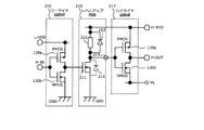
- FIG. 11 is a circuit diagram showing a configuration of the level up circuit.
- FIG. 12 is a circuit diagram showing the configuration of the level down circuit. 11 and 12 show, as peripheral circuits of the level shift circuit, a CMOS circuit transmitting an input signal to the level shift circuit, and a CMOS circuit transmitting an output signal of the level shift circuit to a subsequent stage.
- H-IN, H-OUT, ALM-IN, ALM-OUT, H-VDD, L-VDD, Vs and GND shown in FIGS. 11 and 12 are H-IN, H-OUT and ALM shown in FIG. 10, respectively. -IN, ALM-OUT, H-VDD, L-VDD, Vs and GND.
- the level-up circuit 210 shown in FIG. 11 includes an n-channel insulated gate field effect transistor (MOSFET: Metal Oxide Semiconductor Field Effect Transistor) 211, a level shift resistor 212, and a diode 213.
- the level-up circuit 210 is required when the IGBT 115 of the upper arm of the half bridge circuit is an n-channel type.
- the drain of the n-channel MOSFET 211 is connected to one end of the level shift resistor 212, and the source is grounded.
- the n-channel MOSFET 211 incorporates a body diode 214 connected in antiparallel to the n-channel MOSFET 211.
- a connection point between the n-channel MOSFET 211 and the level shift resistor 212 is an output section 215 of the level up circuit 210.
- the other end of the level shift resistor 212 is connected to H-VDD.
- a diode 213 is connected in parallel to the level shift resistor 212.
- the diode 213 is heated by the heat generated when the potential of H-VDD becomes significantly lower than the potential of GND (when an excessive negative surge voltage (hereinafter referred to as negative surge voltage) is applied).
- negative surge voltage an excessive negative surge voltage
- the diode 213 has a function of preventing application of an excessive voltage to the gate of the CMOS circuit of the high side circuit unit 217 described later when an overvoltage is applied to H-VDD when the n-channel MOSFET 211 is on. Have.
- a Zener diode is frequently used for the diode 213.
- the low side circuit unit 216 is disposed in the front stage of the leveling circuit 210, and the high side circuit unit 217 is disposed in the subsequent stage.
- the low side circuit unit 216 and the high side circuit unit 217 both include a CMOS circuit in which ap channel MOSFET (PMOS) and an n channel MOSFET (NMOS) are connected complementarily.
- the gate of the CMOS circuit of the low side circuit unit 216 is connected to H-IN and receives an input signal transmitted from the HVIC.
- the source of the p-channel MOSFET of the CMOS circuit of the low side circuit unit 216 is connected to L-VDD, and the source of the n-channel MOSFET is grounded.
- the low side circuit unit 216 and the high side circuit 217 may be provided with transmission circuits other than CMOS circuits.
- connection point (output terminal) of the p-channel MOSFET and the n-channel MOSFET constituting the CMOS circuit of the low side circuit unit 216 is connected to the gate of the n-channel MOSFET 211 and transmits the input signal to the level up circuit 210.
- the gate of the CMOS circuit of the high side circuit unit 217 is connected to the output unit 215 of the level up circuit 210, and receives an input of the input signal transmitted from the level up circuit 210.
- the source of the p-channel MOSFET (hereinafter referred to as a second p-channel MOSFET) 130a of the CMOS circuit (hereinafter referred to as a second CMOS circuit) of the high side circuit unit 217 is connected to H-VDD, and an n-channel MOSFET (hereinafter referred to as a second n-channel MOSFET)
- the source of the channel MOSFET 130b is connected to Vs.
- the connection point between the second p-channel MOSFET 130a and the second n-channel MOSFET 130b that constitute the CMOS circuit of the high side circuit unit 217 is connected to H-OUT, and transmits an input signal to the HVIC.
- a level up circuit 210 when the input signal from H-IN is input to the gate of the CMOS circuit of the low side circuit unit 216, the signal passes through the CMOS circuit of the low side circuit unit 216 and the level up circuit 210. Is input to the gate of the n-channel MOSFET 211. In response to the input of the input signal, the n-channel MOSFET 211 is turned on / off, and an output signal is outputted from the output unit 215 of the level up circuit 210 and inputted to the gate of the CMOS circuit of the high side circuit unit 217.
- the CMOS circuit of the high side circuit unit 217 In response to the input of this input signal, the CMOS circuit of the high side circuit unit 217 is turned on / off, and the output signal of the CMOS circuit of the high side circuit unit 217 (the signal raised by the level up circuit 210) starts from H-OUT. It is output. This output signal is converted into a signal based on the potential of the Vs terminal 111 and is input to the gate of the IGBT 115 in the upper arm. In response to the input of this input signal, the IGBT 115 of the upper arm of the half bridge circuit is turned on / off.
- the level down circuit 220 includes a p-channel MOSFET 221, a level shift resistor 222 and a diode 223.
- the drain of the p-channel MOSFET 221 is connected to one end of the level shift resistor 222, and the source is connected to H-VDD.
- the p-channel MOSFET 221 incorporates a body diode 224 connected in antiparallel to the p-channel MOSFET 221.
- a connection point between the p-channel MOSFET 221 and the level shift resistor 222 is an output section 225 of the level down circuit 220.
- the other end of the level shift resistor 222 is grounded.
- a diode 223 is connected in parallel to the level shift resistor 222.
- the diode 223 has a function of preventing the level shift resistor 222 from generating heat and breaking due to heat generated when the potential of H-VDD becomes significantly lower than the potential of GND.
- the diode 223 has a function of preventing application of an overvoltage to the gate of the CMOS circuit of the low side circuit unit 227 described later when the overvoltage is applied to H-VDD when the p-channel MOSFET 221 is turned on.
- the high side circuit unit 226 is disposed in the front stage of the level down circuit 220, and the low side circuit unit 227 is disposed in the subsequent stage.
- the high side circuit unit 226 and the low side circuit unit 227 both include a CMOS circuit in which ap channel MOSFET (PMOS) and an n channel MOSFET (NMOS) are connected in a complementary manner.
- the gate of the CMOS circuit of the high side circuit unit 226 receives an input of an alarm signal formed based on the abnormality signal 110.
- the source of the p-channel MOSFET of the CMOS circuit of the high side circuit unit 226 is connected to H-VDD, and the source of the n-channel MOSFET is connected to Vs.
- the low side circuit unit 227 and the high side circuit 226 may include a transmission circuit other than a CMOS circuit.
- connection point (output terminal) of the p-channel MOSFET and the n-channel MOSFET constituting the CMOS circuit of the high side circuit unit 226 is connected to the gate of the p-channel MOSFET 221 and transmits the input signal to the level down circuit 220.
- the gate of the CMOS circuit of the low side circuit unit 227 is connected to the output unit 225 of the level down circuit 220, and receives an input of the input signal transmitted from the level down circuit 220.
- the source of the p-channel MOSFET of the CMOS circuit of the low side circuit unit 227 is connected to L-VDD, and the source of the n-channel MOSFET is grounded.
- the connection point between the p-channel MOSFET and the n-channel MOSFET constituting the CMOS circuit of the low side circuit unit 227 is connected to ALM-OUT, and an output signal is output from ALM-OUT to the outside.
- a level down circuit 220 when an alarm signal based on the abnormal signal 110 is input to the gate of the CMOS circuit of the high side circuit unit 226, the signal is level down via the CMOS circuit of the high side circuit unit 226.
- the signal is input to the gate of the p-channel MOSFET 221 of the circuit 220.
- the p-channel MOSFET 221 is turned on / off, and an output signal is outputted from the output section 225 of the level down circuit 220 and inputted to the gate of the CMOS circuit of the low side circuit section 227.
- the CMOS circuit of the low side circuit unit 227 is turned on / off, and the output signal of the CMOS circuit of the low side circuit unit 227 (alarm signal leveled down by the level down circuit 220) is output from ALM-OUT. Be done.
- FIG. 13 is a cross-sectional view showing the structure of a conventional high voltage integrated circuit device.
- H-IN, H-OUT, H-VDD, L-VDD, Vs and GND are respectively H-IN, H-OUT, H-VDD, L-VDD, Vs and GND of the HVIC shown in FIG. And corresponding terminals.
- n ⁇ type well regions 102 and 104, n type well region 103 and p type are provided on the surface layer of the front surface of the p type semiconductor substrate 101 connected to GND.
- Well regions 105 are selectively provided, respectively.
- the n ⁇ -type well region 104 surrounds the n-type well region 103, and the n ⁇ -type well region 102 is provided outside the n ⁇ -type well region 104 (on the chip outer peripheral side).
- p-type well region 105, n - is provided between the type well region 104, n - - -type well region 102 and n contact with the type well region 104 - -type well region 102 and n.
- FIG. 13 shows a first CMOS circuit (p-channel MOSFET (hereinafter, referred to as first p-channel MOSFET) 120a and n-channel MOSFET (hereinafter, referred to as first n-channel MOSFET) 120b) constituting the low side circuit unit 216.
- first CMOS circuit p-channel MOSFET (hereinafter, referred to as first p-channel MOSFET) 120a and n-channel MOSFET (hereinafter, referred to as first n-channel MOSFET) 120b) constituting the low side circuit unit 216.
- first n-channel MOSFET p-channel MOSFET
- first n-channel MOSFET n-channel MOSFET
- the 1p channel MOSFET120a is, n - -type well region 102, n + -type contact region 122, p + -type source region 123, p + -type drain region 124 and a gate electrode 125 common lateral MOS gate (metal - oxide A film-insulated gate formed of a semiconductor), a source electrode 161, and a drain electrode 162 are provided.
- the gate electrode 125 is connected to H-IN.
- the source electrode 161 is connected to L-VDD.
- the drain electrode 162 is connected to the drain electrode 164 of the first n-channel MOSFET 120b.
- the first n-channel MOSFET 120 b has a general lateral MOS gate structure including a p-type offset region 121, an n + -type drain region 126, an n + -type source region 127, a p + -type contact region 128 and a gate electrode 129. , Drain electrode 164.
- the gate electrode 129 is connected to the gate electrode 125 of the first p-channel MOSFET 120a and is connected to H-IN.
- the source electrode 163 is connected to GND.
- the drain electrode 164 is connected to the drain electrode 162 of the first p-channel MOSFET 120a.
- the second p-channel MOSFET 130 a has a general lateral MOS gate structure including an n-type well region 103, an n + -type contact region 132, a p + -type source region 133, a p + -type drain region 134 and a gate electrode 135. , Drain electrode 166.
- the gate electrode 135 is connected to the output unit 215 of the level up circuit 210.
- a level shift resistor 212 and a diode 213 are connected in parallel between H-VDD and the output unit 215.
- the source electrode 165 is connected to H-VDD.
- the drain electrode 166 is connected to H-OUT.
- the second n-channel MOSFET 130 b has a general lateral MOS gate structure including a p-type offset region 131, an n + -type drain region 136, an n + -type source region 137, a p + -type contact region 138 and a gate electrode 139. , Drain electrode 168.
- the gate electrode 139 is connected to the gate electrode 135 of the second p-channel MOSFET 130a (not shown).
- the source electrode 167 is connected to Vs.
- the drain electrode 168 is connected to the drain electrode 166 of the second p-channel MOSFET 130a and is connected to H-OUT.
- the n-channel MOSFET 211 constituting the level-up circuit 210 is arranged from the n-type well region 103 to the n ⁇ -type well region 104 and the p-type well region 105 in contact with the n ⁇ -type well region 104.
- the n-channel MOSFET 211 constituting the level-up circuit 210 includes an n-type well region 103, an n -- type well region 104, a p-type well region 105, an n + -type source region 141, an n + -type drain region 142, and a p + -type contact region 143, a gate electrode 144, a source electrode 145 and a drain electrode 146 are provided.
- the p-type well region 105 functions as a base region.
- an n + -type source region 141 and a p + -type contact region 143 are selectively provided inside the n-type well region 103. Inside the n-type well region 103, an n + -type drain region is selectively provided.
- a gate electrode 144 is provided on the surface of a portion of the p-type well region 105 sandwiched by the n + -type source region 141 and the n ⁇ -type well region 104 via a gate insulating film. The gate electrode 144 is connected to the drain electrode 162 of the first p-channel MOSFET 120 a and the drain electrode 164 of the first n-channel MOSFET 120 b.
- Source electrode 145 is in contact with n + -type source region 141 and p + -type contact region 143. In addition, the source electrode 145 is connected to GND.
- the drain electrode 146 is in contact with the n + -type drain region. Further, the drain electrode 146 is connected to the level shift resistor 212 by a surface metal wiring (not shown), and is connected to H-VDD via the level shift resistor 212.
- the connection portion between the drain electrode 146 and the level shift resistor 212 serves as the output portion 215 of the level up circuit 210.
- the output from the output unit 215 is a low potential when the n-channel MOSFET 211 is on, and is a high potential when the n-channel MOSFET 211 is off. Therefore, the HVIC 200 can perform a level shift operation which is signal transmission between different reference potentials.
- Reference numeral 147 denotes ap + -type contact region
- reference numeral 148 denotes a pickup electrode.
- the source electrode (hereinafter referred to as a first pickup electrode) 145 of the n-channel MOSFET 211 uses electrons injected into the p-type well region 105 at the time of negative surge voltage generation as ap + -type contact region (hereinafter referred to as a first high concentration region). ) Functions as a pickup electrode pulled out from 143).
- an n + -type contact region (hereinafter referred to as a second high concentration region) 151 is formed near the boundary with the n ⁇ -type well region 104. It is provided.
- the second pickup electrode 152 is in contact with the second high concentration region 151.
- the second pickup electrode 152 is connected to H-VDD and has a function of extracting holes injected into the n-type well region 103 from the second high concentration region 151 when a negative surge voltage is generated.
- a bridge circuit configured by combining half-bridge circuits configured with switching power devices (IGBTs 114 and 115) using such an HVIC 200 as a drive element is a large capacity plasma display panel (PDP) in addition to an inverter for motor control. It is widely used in many fields such as plasma display panel), power source applications such as liquid crystal panels, and inverters for home appliances such as air conditioners and lighting. In addition to the IGBTs, power MOSFETs are also used as switching power devices forming the half bridge circuit. These motors, lighting, etc. become the L load 118 as described above. Therefore, Vs and H-VDD of the HVIC 200 are adversely affected by the parasitic inductance component and the like due to the wiring on the printed circuit board and the cable up to the L load 118.
- V S0 L 0 ⁇ dI / dt (1)
- the parasitic pn diode 171 is composed of a p-type semiconductor substrate 101 and an n-type well region 103.
- the parasitic pn diode 172 is composed of a p-type well region 105 and an n ⁇ -type well region 104.
- V supply is a battery voltage across the low voltage power supply 113 or a bootstrap capacitor (not shown).
- V fd is a forward voltage drop of the parasitic pn diodes 171 and 172.
- the negative surge voltage V S0 applied to the Vs terminal 111 is, for example, about -30 V, and the application period thereof is about several hundred ns to about 500 ns.
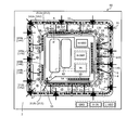
- FIG. 14 is a plan view showing a planar layout of the high voltage integrated circuit device of FIG.
- a high potential region in which the high side circuit units 217 and 226 are disposed a low potential region in which the low side circuit units 216 and 227 are disposed, and a region to which a common potential (GND potential) is applied (hereinafter referred to as Shows a HVJT 201 including a common potential region).
- GND potential common potential
- FIG. 14 shows a Vs potential region 181 connected to the Vs pad and an H-VDD potential region 182 connected to the H-VDD pad.
- the Vs potential region 181 is a region which is electrically connected to the Vs pad and to which a potential of Vs is applied. Specifically, the Vs potential region 181 is the p-type offset region 131 and the p + -type drain region 134 of the second n-channel MOSFET 130 b constituting the logic unit of the high side circuit unit 217.
- the H-VDD potential region 182 is a region which is electrically connected to the H-VDD pad and to which the H-VDD potential is applied.
- the H-VDD potential region 182 is a region in which the n + -type contact region 132 and the p + -type source region 133 of the second p-channel MOSFET 130a of the high side circuit unit 217 are arranged.
- an n ⁇ -type well region 104 which is a breakdown voltage region, is disposed in contact with the n-type well region 103 and surrounding the n-type well region 103.
- a second high concentration region 151 which is an n + -type contact region is provided annularly along the outer periphery of the n-type well region 103. .
- the second high concentration region 151 is disposed apart from the n ⁇ -type well region 104.
- the second pickup electrode 152 is disposed on the second high concentration region 151.
- the second pickup electrode 152 is connected to the H-VDD pad.
- a first high concentration region 143 which is a p + -type contact region, is disposed annularly along the outer periphery of the n ⁇ -type well region 104.
- the first pickup electrode 145 is disposed on the first high concentration region 143.
- the black squares respectively arranged as the first and second pickup electrodes 145 and 152 are the first and second pickup electrodes 145 deposited on an interlayer insulating film or a protective film (not shown) covering the front surface of the chip. , 152, which are embedded in the contact holes. That is, black squares indicating the first and second pickup electrodes 145 and 152 are contacts (electrical contact portions) with the first and second high concentration regions 143 and 151.
- the first and second pickup electrodes 145 and 152 are annularly disposed on the first and second high concentration regions 143 and 151, respectively.
- the HVJT 201 is configured.
- a level shift circuit extends from the n-type well region 103 to the n - type well region 104 and the p-type well region 105 in a region including the corner portion of the n - type well region 104 having a substantially rectangular annular planar shape. It is arranged.
- FIG. 14 shows the n + -type drain region 142, the gate electrodes 144 (144a and 144b) and the drain electrode 146 of the n-channel MOSFET 211 of the level-up circuit 210.
- the n-channel MOSFET 211 constitutes an RS (Reset-Set) flip-flop that holds the output signal (gate signal) to the IGBT 115 in a low level or a high level.
- the n-type well region 103 has a substantially concave square planar shape in which one corner is recessed inward (toward the chip center), and the n-type well region 103 of the n ⁇ -type well region 104 is recessed.
- An n + -type drain region 142 is disposed in the ridge portion.
- a drain electrode 146 is disposed on the n + -type drain region 142.
- the n + -type drain region 142 and the drain electrode 146 are disposed for each of the set and reset n-channel MOSFETs 211.
- gate electrodes 144a and 144b receiving the input of the set signal and the reset signal are arranged.
- the gate electrodes 144a and 144b are disposed on straight portions corresponding to two consecutive sides sharing one corner of the substantially rectangular annular p-type well region 105, respectively.
- an n -- type well region 102 which is a low potential region, is disposed in contact with the p-type well region 105 and surrounding the p-type well region 105.
- a logic unit (not shown) of the low side circuit unit 216, a GND pad, an H-IN pad, and an L-VDD pad are arranged in the n ⁇ -type well region 102.
- a broken line surrounding the periphery of each pad indicates a region into which the current flowing through the parasitic pn diode flows (the same applies to FIGS. 1, 3 to 5).
- the region indicated by a broken line finer than the broken line surrounding each pad is the drain region 146 of the n-channel MOSFET 211 and the pickup electrode It is a wiring layer connecting the 152 and the H-VDD pad.
- the Vs potential region 181 is located near the outer periphery of the n-type well region 103. It is disposed close to the second high concentration region 151. That is, one side 185 of the substantially rectangular Vs potential region 181 opposes one side of the inner periphery of the substantially rectangular second high concentration region 151 surrounding the periphery of the n-type well region 103. As a result, the distance between the Vs potential region 181 and the HVJT 201 can be minimized on one side (hereinafter referred to as an opposing location) 185 of the second high concentration region 151 facing the Vs potential region 181.
- a parasitic diode in the HVIC chip is used to protect the HVIC driving the half bridge type power transistor in anticipation of an excessive negative swing (a negative surge voltage is applied) at the output node. And in series with, and between the substrate of the HVIC chip and the ground potential terminal, during a negative voltage spike (negative surge) flowing to the parasitic diode of the HVIC due to a negative voltage transient at the output node.
- a circuit provided with a resistor for limiting current has been proposed (see, for example, Patent Document 1 below).
- a level shift resistor As another HVIC, a level shift resistor, a current limiting resistor, and a level up circuit between the high potential side of the high voltage power supply and the low potential (ground potential) side from the high potential side of the high voltage power supply.
- a device has been proposed in which the switching elements (the drain is on the high potential side) in series are connected in series in the order, and the portion between the level shift resistor and the current limiting resistor is the output of the leveling circuit (see, for example, Patent Document 3 below).
- a current limiting resistor is connected to the current path between the high potential side (H-VDD) and the low potential side (GND) of the low voltage power supply of the level shift circuit based on the potential of the Vs terminal.
- the body diode of the n-channel MOSFET constituting the level-up circuit or the parasitic pn diode itself of the HVIC may be destroyed by an overcurrent, or the place where the current capacity of the level shift circuit is small may be destroyed by an overcurrent. It is preventing.
- a device has been proposed in which a high breakdown voltage diode is provided between the common ground node and the virtual ground (intermediate potential) node of the high potential side reference potential using a common substrate region inside the HVIC.
- a virtual ground node of a high potential side reference potential is provided by providing a high breakdown voltage diode between a terminal (Vs terminal) of a high potential side reference potential and a substrate region at a common ground potential (GND potential).
- the double resurf structure is partially formed by thinning the contact of the HVJT at a location close to the high potential side reference potential region (Vs potential region) or widening the withstand voltage region constituting the HVJT.
- Vs potential region the high potential side reference potential region
- Patent Document 5 the amount of carriers injected into the high potential side reference potential region is reduced as the high potential side power supply voltage decreases due to the undershoot of the negative voltage.
- an n -- type diffusion region which is a low breakdown voltage region is annularly formed on the p -- type semiconductor substrate, and an n-type diffusion region constituting the HVJT is annularly formed in contact with the inner side.
- a device provided with an island-like n-type diffusion region which is a high withstand voltage region sandwiching a p ⁇ -type semiconductor substrate having a predetermined width on the inner side is proposed (for example, Patent Document 6 (paragraph 0045, eighth See Figure).
- Patent Document 6 proposes a structure in which an n-type diffusion layer constituting an HVJT and an n-type diffusion layer in which a high side circuit portion is arranged are divided by a ring p -- type diffusion layer.
- the above-described conventional HVIC has the following problems.
- the high potential side Vss of the high voltage power supply (main circuit power supply) is about 1200 V, The case where the potential is higher by about 15 V than the potential of Vs will be described as an example.
- the L load 118 tries to maintain the current flowing to the power conversion device (the L load 118 delays the current phase with respect to the AC voltage).
- a current flows in the L load 118 via the FWD 116 connected in parallel to the IGBT 114 in the lower arm.
- the potential of the Vs terminal 111 becomes lower than the GND potential, and becomes, for example, about -30V.
- the p-type semiconductor substrate 101 and the p-type well region 105 are at the GND potential. Therefore, the potential of the Vs terminal 111 decreases until both the n-type well region 103 and the n ⁇ -type well region 104 constituting the CMOS circuit of the logic portion of the high side circuit portion 217 of the level up circuit 210 become lower than the GND potential. In this case, the parasitic pn diodes 171 and 172 become forward biased and a large current flows.
- This current is input from the high side circuit unit 217 to the IGBT 115 through the n-type well region 103, and flows to the L load 118 through the gate-emitter capacitance of the IGBT 115. Since there is no resistance component for limiting the current in this current path (path), an extremely large pulse current is obtained. This pulse current may cause the HVIC 200 to be broken or malfunction.
- the cathode is removed from the p-type well region 105 that constitutes the anode of the parasitic pn diode 172. Holes are injected into the n -- type well region 104 to be formed.
- the resistance of the n ⁇ type well region 104 sandwiched between the Vs potential region 181 and the p type well region 105 (parasitic pn diode 172
- the cathode resistance is smaller than the other parts of the n ⁇ -type well region 104. Therefore, in the opposite portion 185 where the distance between the HVJT 201 and the Vs potential region 181 is narrow, the amount of hole injection from the p-type well region 105 to the n ⁇ -type well region 104 is the same as that of the n ⁇ -type well region 104. There will be more than places.
- the p-type offset region which is a Vs potential region 181 having a negative potential with respect to the GND potential, passes directly under the second high concentration region 151 (on the back surface side of the substrate) of holes entering the n ⁇ type well region 104. 131 and flows toward the p + -type drain region 134. The holes that have entered the p-type offset region 131 are extracted from the p + -type contact region 138 to the Vs terminal 111.
- n + -type source region 137 composed of n + -type source region 137, p-type offset region 131 and the n-type well region 103 It becomes the gate current of the parasitic npn transistor. Therefore, there is a possibility that the parasitic npn transistor is turned on to cause the logic unit of the high side circuit unit 217 to malfunction.
- n + holes flowed down to just below the source regions 137, n + -type source region 137, p-type offset region 131, n-type well region 103 and p-type parasitic thyristor ON comprising a semiconductor substrate 101 (latch If the high side circuit portion 217 is broken, the high side circuit portion 217 may be broken.
- the high side circuit unit 217 may malfunction.
- the parasitic pn diode 171 has a high anode resistance because the specific resistance of the p-type semiconductor substrate 101 to be the anode is high. Therefore, the injection of holes from the p-type semiconductor substrate 101 to the n-type well region 103 is very small.
- Patent Document 1 the amount of current is suppressed by connecting a resistor that limits current between the substrate and the ground terminal, but other points There is no mention of connecting a resistor to. Also, since this resistor is formed of a polysilicon layer, when a large pulse current (several amps to several tens of amps) due to a negative surge voltage transiently flows to the parasitic diode between the Vs terminal and the ground terminal. In addition, the polysilicon layer constituting the resistor may be thermally melted and destroyed due to an overcurrent.
- Patent Document 2 describes a resistor and a layout for limiting the current of the body diode of the MOSFET constituting the level shift circuit and the parasitic pn diode of the HVIC when the potential of H-VDD becomes a negative potential due to the L load.
- Patent Document 3 does not describe preventing a malfunction (incorrect inversion) due to a parasitic operation of the high side circuit unit based on the potential of the Vs terminal.
- Patent Document 4 describes the provision of a high breakdown voltage diode between a node (potential point) of a bootstrap power supply potential (potential of H-VDD) and a substrate region at a common ground potential (GND potential). Absent.
- Patent Document 5 when the negative surge voltage is high or when the application period of the negative surge voltage is long, a large amount of carriers are injected also into the Vs potential region, so malfunction of the high side circuit or The effect of preventing destruction can not be obtained. For this reason, the effect is limited.
- a high breakdown voltage n-channel RESURF MOSFET constituting a level shift circuit is disposed in an n-type diffusion layer constituting an HVJT, and this n-type diffusion layer is a drain drift region or a drain It corresponds to the area. For this reason, holes (current) are injected from the n-type diffusion layer constituting the HVJT into the level shift circuit by the negative surge voltage, and the internal devices and interconnections of the level shift circuit are heated due to excess current and are destroyed. Excessive injection of holes may destabilize the potential of the drain node (the drain potential point of the high breakdown voltage n-channel resurf MOSFET), which may cause the level shift circuit to malfunction.
- An object of the present invention is to provide a semiconductor integrated circuit device capable of preventing a malfunction or destruction in order to solve the above-mentioned problems of the prior art.
- a semiconductor integrated circuit device has the following features.
- a first second conductivity type well region is provided in a surface layer on one surface of the first conductivity type semiconductor layer.
- a potential equal to or higher than a second potential is supplied to the first second conductivity type well region.
- a second second conductivity type well region is provided in contact with the first second conductivity type well region in a surface layer on one surface of the first conductivity type semiconductor layer.
- the second second conductivity type well region surrounds the periphery of the first second conductivity type well region.
- the impurity concentration of the second second conductivity type well region is lower than the impurity concentration of the first second conductivity type well region.
- a first conductivity type well region is provided in contact with the second second conductivity type well region in a surface layer on one surface of the first conductivity type semiconductor layer.
- the first conductivity type well region surrounds the periphery of the second conductivity type well region.
- a separation region is provided which electrically separates a predetermined region in the first second conductivity type well region and a region outside the predetermined region.
- a first second conductivity type high concentration region is provided outside the separation region inside the first second conductivity type well region or the second second conductivity type well region.
- the impurity concentration of the first second conductivity type high concentration region is higher than the impurity concentration of the first second conductivity type well region.
- a second high conductivity region of the second conductivity type is provided inside the first second conductivity type well region or the second second conductivity type well region inside the separation region.
- the impurity concentration of the second second conductivity type high concentration region is higher than the impurity concentration of the first second conductivity type well region.
- the first electrode is in contact with the first second conductivity type high concentration region, and the first second conductivity type well region or the second second conductivity type region via the first second conductivity type high concentration region.
- a third potential higher than the second potential is applied to the conductive well region.
- the second electrode is in contact with the second high conductivity region of the second conductive type, and the first well region of the second conductive type or the second second conductive region through the high concentration region of the second second conductive type.
- the third potential is applied to the conductive well region.
- a semiconductor integrated circuit device is characterized in that, in the above-mentioned invention, the separation region is disposed in a ring shape surrounding the predetermined region.
- the isolation region passes between the predetermined region and the first second conductivity type high concentration region, and the second second It is arranged to cross the conductive well region to reach the first conductive well region, and separate the predetermined region from the region outside the first second conductive high concentration region.
- a semiconductor integrated circuit device is characterized in that, in the above-mentioned invention, the separation region is a first conductivity type semiconductor region or a dielectric region.
- the semiconductor integrated circuit device further has the following features in the above-described invention.
- a third second conductivity type well region is provided on the opposite side to the first second conductivity type well region with the first conductivity type well region interposed therebetween. It is provided.
- a first circuit portion is provided in the third region of the second conductivity type.
- a fourth electric potential higher than the first electric potential is supplied to the first circuit unit from a first low voltage power supply based on the first electric potential.
- a second circuit portion is provided in the first second conductivity type well region. The third potential is supplied to the second circuit unit from a second low voltage power source based on the second potential.
- a third circuit portion is provided in the second conductive well region and the first conductive well region.
- the third circuit unit is connected between the first circuit unit and the second circuit unit, converts a voltage level of a signal input from the first circuit unit, and outputs the voltage level to the second circuit unit. .
- the second circuit unit outputs a gate signal of the high potential side of the two transistors connected in series based on the signal output from the third circuit unit.
- the second potential is between the high potential side potential of the main circuit power supply of the two transistors connected in series and the first potential. It is characterized by having a floating potential.
- a semiconductor integrated circuit device is characterized in that, in the above-described invention, the second potential is supplied to the predetermined region.
- the second potential drops in the negative direction, and the predetermined region where the second circuit on the high side is disposed and the second region of the second conductivity type that constitutes the high withstand voltage junction termination region are transient.
- Parasitic pn diode having the first conductivity type well region constituting the high breakdown voltage junction termination region as an anode and the second second conductivity type well region as a cathode when the potential is lower than the first potential (minimum potential).
- Current injection hole carrier injection
- transient injection of holes into the predetermined region of the second potential can be suppressed.
- the semiconductor integrated circuit device of the present invention it is possible to reduce the amount of hole injection due to negative surge voltage and prevent malfunction or destruction of the high side circuit portion without increasing the chip area. Play.
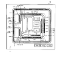
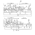
- FIG. 1 is a plan view showing a planar structure of the high voltage integrated circuit device according to the first embodiment.
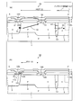
- FIG. 2 is a cross-sectional view showing a cross-sectional structure taken along line AA ′ and line CC ′ of FIG.
- FIG. 3 is an explanatory view showing the behavior of carriers when a negative surge voltage is applied to the high voltage integrated circuit device of FIG.
- FIG. 4 is a cross-sectional view showing the structure of the main part of the high voltage integrated circuit device according to the second embodiment.
- FIG. 5 is a cross-sectional view showing the structure of the main part of another example of the high voltage integrated circuit device according to the second embodiment.
- FIG. 6 is a cross-sectional view showing the structure of the main part of the high voltage integrated circuit device according to the third embodiment.
- FIG. 1 is a plan view showing a planar structure of the high voltage integrated circuit device according to the first embodiment.
- FIG. 2 is a cross-sectional view showing a cross-sectional structure taken along line
- FIG. 7 is a cross-sectional view showing the structure of the main part of the high voltage integrated circuit device according to the fourth embodiment.
- FIG. 8 is a cross-sectional view showing a cross-sectional structure taken along line BB 'in FIG.
- FIG. 9 is a cross-sectional view showing the structure of the main part of the high voltage integrated circuit device according to the fifth embodiment.
- FIG. 10 is a circuit diagram showing a connection configuration of the high voltage integrated circuit device.
- FIG. 11 is a circuit diagram showing a configuration of the level up circuit.
- FIG. 12 is a circuit diagram showing the configuration of the level down circuit.
- FIG. 13 is a cross-sectional view showing the structure of a conventional high voltage integrated circuit device.
- FIG. 14 is a plan view showing a planar layout of the high voltage integrated circuit device of FIG.
- n and p in the layer or region having n or p, it is meant that electrons or holes are majority carriers, respectively.
- + and-attached to n and p mean that the impurity concentration is higher and the impurity concentration is lower than that of the layer or region to which it is not attached, respectively.
- Embodiment 1 The structure of the semiconductor integrated circuit device according to the first embodiment will be described with reference to FIGS. 1, 2, 7 to 9 by taking a self isolated high breakdown voltage integrated circuit device (HVIC) as an example.
- FIG. 1 is a view showing a planar structure of the high voltage integrated circuit device according to the first embodiment.
- FIG. 2 is a cross-sectional view showing a cross-sectional structure taken along line AA ′ and line CC ′ of FIG.
- the HVIC 50 according to the first embodiment is a drive element corresponding to the HVIC constituting the power conversion device shown in FIG. 10, and has a function of controlling on / off of the IGBTs (transistors) 114 and 115 of the half bridge circuit.
- connection configuration of the HVIC 50 (circuit configuration of the power conversion device), the circuit configuration of the level shift function (level shift circuit) of the HVIC 50, and the method of driving the IGBTs 114 and 115 by the HVIC 50 may be the same as, for example, conventional (See the description of Figures 10-12).
- the HVIC 50 includes a high potential region, a low potential region, and a high voltage junction termination region (HVJT) 21 on a p-type semiconductor substrate (first conductive semiconductor layer) 1.
- the high potential region is a region to which the H-VDD potential (third potential) of the HVIC 50 and the potential (second potential) of Vs are applied.
- the high potential region is the n-type well region (first second conductivity type well region) 3 disposed on the front surface side of the p-type semiconductor substrate 1.
- a high side circuit unit (second circuit unit) which is a peripheral circuit of the level shift circuit is arranged.
- the low potential region is a region to which L-VDD (fourth potential) of the HVIC 50 or the potential (first potential) of GND is applied.
- the low potential region is an n ⁇ -type well region (third second conductivity-type well region) 2 disposed outside the n-type well region 3 (on the chip outer peripheral side).
- a low side circuit unit (first circuit unit) which is a peripheral circuit of the level shift circuit is arranged.
- the HVJT 21 is a region including a withstand voltage region and a common potential region, and may be provided with, for example, a level shift circuit.
- the breakdown voltage region is an n ⁇ -type well region (second second conductivity type well region) 4 disposed between the n-type well region 3 and the n ⁇ -type well region 2.
- the common potential area is an area to which a common potential (for example, GND potential (ground potential)) is applied.
- the common potential region is the p-type well region (first conductivity type well region) 5 disposed between the n ⁇ -type well region 4 and the n ⁇ -type well region 2.
- the common potential will be described as the GND potential.
- the cross-sectional structure of the level shift circuit and the peripheral circuit of the level shift circuit is, for example, similar to that of the conventional HVIC (see FIG. 13).
- the HVIC 50 includes the level up circuit (third circuit) 210 and its peripheral circuits (the high side circuit unit 217 and the low side circuit unit 216) will be described as an example here, even though the HVIC 50 includes the level down circuit. Good.
- H-VDD is a terminal connected to the high potential side of the low voltage power supply 113 which is a high side drive power supply based on the potential of the Vs.
- L-VDD is a terminal connected to the high potential side of the low voltage power supply 112 which is a low side drive power supply based on the potential of GND.
- Vs is a terminal of an intermediate potential (floating potential) that fluctuates from the potential of the high potential side Vss of the high voltage power supply (main circuit power supply) to the potential of GND.
- GND is a ground (ground) terminal.
- H-VDD, L-VDD, Vs and GND in FIG. 1 are terminals corresponding to H-VDD, L-VDD, Vs and GND shown in FIG. 10, respectively (the same applies to FIGS. 3 to 5).
- n-type well region 3 which is a high potential region, for example, the high-side circuit portions 217 and 226 of the level-up circuit 210, H-VDD pads (terminals), H-OUT pads, Vs pads, n + -type contact regions
- the second and third high concentration regions (first and second second conductivity type high concentration regions) 51 and 54 and the second and third pickup electrodes (first and second electrodes) 52 and 55 are disposed.
- a Vs potential region (predetermined region) 81 is a region which is electrically connected to the Vs pad and to which a potential of Vs is applied.
- a wiring layer connecting the Vs potential region 81 and the Vs pad is indicated by a broken line connecting the Vs potential region 81 and the Vs pad.
- the Vs potential region 81 includes the p-type offset region 131, the n + -type drain region 136, the n + -type source region 137, and the p + -type contact region 138 of the second n-channel MOSFET 130b constituting the high side circuit unit 217. And a region where the p + -type drain region 134 and the like of the second p-channel MOSFET 130 a are disposed.
- the H-VDD potential region 82 is a region electrically connected to the H-VDD pad and to which the H-VDD potential is applied.
- the potential of the H-VDD pad is the power supply voltage of the circuit disposed in the n-type well region 3.
- the H-VDD potential region 82 is a region in which the n + -type contact region 132, the p + -type source region 133, and the like of the second p-channel MOSFET 130a of the high side circuit unit 217 are disposed.
- the Vs potential region 81 and the H-VDD potential region 82 are in a direction along one side 13 a of the outer periphery of the n-type well region 3 having a substantially rectangular planar shape (hereinafter referred to as a first direction). In the form of a straight line extending in Further, in FIG. 1, the Vs potential region 81 and the H-VDD potential region 82 are disposed in parallel in the first direction and in a direction orthogonal to the first direction (hereinafter, referred to as a second direction). The state is illustrated. Although the Vs potential region 81 and the H-VDD potential region 82 are shown separately in FIG. 1, in actuality, each region disposed in the Vs potential region 81 and the H-VDD potential region 82 is an n-type well region 3 is placed on top of the other.
- H-VDD pad, H-OUT Pads and Vs pads are arranged on the outer periphery of the n-type well area 3.
- H-VDD pad, H-OUT pad, and Vs pad are sequentially arranged in parallel in the first direction.
- Each pad (H-VDD pad, H-OUT) is provided on the side 13b opposite to the side 13a on the side where the Vs potential area 81 and the H-VDD potential area 82 are disposed on the outer periphery of the n-type well area 3.
- a third high concentration region 54 is disposed outside the pad and the Vs pad) and facing each pad.
- the third high concentration region 54 has a linear planar shape extending in a direction (first direction) along one side 13 b of the outer periphery of the n-type well region 3.
- a third side 13c is provided along one side 13c facing the Vs pad.
- a high concentration region 54 is disposed.
- the third high concentration region 54 disposed along one side 13 c of the outer periphery of the n-type well region 3 is disposed not to face, for example, the Vs potential region 81.
- the third high concentration regions 54 disposed along the two sides 13 b and 13 c of the outer periphery of the n-type well region 3 are disposed apart from each other.
- the third high concentration region 54 is not disposed at one corner (corner) shared by the two sides 13 b and 13 c on the outer periphery of the n-type well region 3.
- the third pickup electrode 55 is arranged annularly along the third high concentration region 54 on the third high concentration region 54.
- the third pickup electrode 55 is connected to the H-VDD pad.
- the third high concentration region 54 is formed for the purpose of stabilizing the potential of the n-type well region 3 and is desirably formed as much as possible in a region where a circuit is not formed. In addition, the third high concentration region 54 may not be provided.
- ap ⁇ -type region (hereinafter referred to as “p ⁇ -type separation region”) 53 is disposed annularly along the outer periphery of the n-type well region 3.
- the p ⁇ -type separation region 53 joins and separates the inside of the n-type well region 3.
- p - type isolation region 53, the n-type well region 3, Vs potential region 81, H-VDD potential region 82, like the third high concentration region 54 and the respective pads are arranged p - type isolation
- the part on the inner side (the chip center side) than the region 53 and the part on the outer side (the chip outer peripheral side) than the p ⁇ -type separation area 53 are bonded and separated.
- the p ⁇ -type separation region 53 is preferably arranged as close to the interface with the n ⁇ -type well region 4 as possible. The reason is that a region surrounded by the p ⁇ -type separation region 53 in which holes are not substantially injected, that is, a region in which the Vs potential region 81, the H-VDD potential region 82, and the like are arranged can be secured as large as possible. It is.
- the second high concentration region 51 is selectively Is located in The second high concentration region 51 is not in contact with the p ⁇ -type separation region 53.
- the second high concentration regions 51 are disposed apart from each other along the sides 13 a to 13 d of the outer periphery of the n-type well region 3, and arranged at the corner portions of the n-type well region 3. It has not been.
- the second pickup electrodes 52 are disposed on the respective second high concentration regions 51 along the second high concentration regions 51 respectively.
- the second pickup electrode 52 is connected to the H-VDD pad in the same manner as the second pickup electrode of the conventional HVIC.
- two n + -type drain regions 142a and 142b arranged along the side 13a of the outer periphery of the n-type well region 3 form a level-up circuit 210 with the n ⁇ -type well region 4 as a drift region. It is an n + -type drain region of the n-channel MOSFET 211 for reset and reset.
- the two n + -type drain regions 142a and 142b disposed along the side 13a of the outer periphery of the n-type well region 3 are sides of the outer periphery of the n-type well region 3 via the level shift resistors 212a and 212b, respectively. It is connected to a second high concentration region 51 disposed along the sides 13c and 13d continuous to 13a.
- Level shift resistance 212 (212 a, 212 b) is a second high concentration region arranged along n + type drain region 142 of n type well region 3 and sides 13 c and 13 d of the outer periphery of n type well region 3. It is an internal resistance comprised by the part pinched
- Each n + -type drain region 142a, On 142b, respectively n + -type drain region 142a, the drain electrode 146a along 142b, 146b are arranged.
- the drain electrodes 146a and 146b are connected to the output unit 215 in the same manner as the conventional drain electrode 146.
- the source region of the n-channel MOSFET 211 is formed inside the p-type well region 5 (not shown) in the same manner as the conventional n + -type source region 141.
- a level shift circuit can be operated by turning on the n-channel MOSFET 211 and supplying a current to the level shift resistors 212 (212 a and 212 b) to lower the voltage of the output unit 215.
- the level shift resistance 212 is not limited to the internal resistance, and may be another resistance element, for example, a polycrystalline silicon layer formed on the n-type well region 3 via an insulating film.
- n ⁇ -type well region 4 is disposed around the n-type well region 3 so as to be in contact with the n-type well region 3 and to surround the n-type well region 3.
- p-type well region 5 is disposed a common potential region.
- the p + -type contact region (first high concentration region) 143 is disposed annularly along the outer periphery of the n ⁇ -type well region 4.
- the first pickup electrode 145 is disposed annularly along the first high concentration region 143 above the first high concentration region 143.
- the first pickup electrode 145 is connected to GND.
- the n + -type source region 141 of the n-channel MOSFET 211 is also connected to the first pickup electrode 145.
- the first and second pickup electrodes 145 and 52 are simplified, and contacts of the first and second pickup electrodes 145 and 52 deposited on an interlayer insulating film or a protective film (not shown) covering the chip front surface are illustrated.
- the part embedded in the hole is shown by a black square. That is, each black square indicating the first and second pickup electrodes 145 and 52 is a contact (electrical contact portion) with the first and second high concentration regions 143 and 51, respectively.
- the first and second high concentration regions 143 and 51 may be used.
- An extending strip of contacts may be provided.
- the HVJT 21 is formed by the portion between the second high concentration region 51 and the p ⁇ -type separation region 53). That is, the HVJT 21 is formed of portions of the first and second high concentration regions 143 and 51, the n ⁇ -type well region 4, and the p-type well region 5 inside the first high concentration region 143.
- the n + -type drain region 142 (142a, 142b), the gate electrode (indicated by reference numerals 144a, 144b), and the level shift resistor 212 (212a, 212b) of the n-channel MOSFET 211 of the level-up circuit 210 of FIG. Show.
- n-channel MOSFETs 211 for setting and resetting are respectively arranged.
- the n + -type drain regions 142 a and 142 b of the set and reset n-channel MOSFETs 211 are both arranged on the n ⁇ -type well region 4.
- Gate electrodes 144a and 144b receiving the input of the set signal and the reset signal are disposed on the n ⁇ -type well region 4 and the p-type well region 5, respectively.
- Gate electrodes 144a and 144b are disposed on the surface of p type well region 5 via an insulating film (not shown) so as to face n + type drain regions 142a and 142b, respectively.
- an n ⁇ -type well region 2 which is a low potential region is arranged in contact with the p-type well region 5 and surrounding the p-type well region 5.
- a logic portion (not shown) of the low side circuit portion 216 of the level-up circuit 210, a GND pad, an H-IN pad, an L-VDD pad, and the like are arranged in the n ⁇ -type well region 2.
- a region shown by a broken line (broken line surrounding the second high concentration region 51 and the H-VDD pad) finer than the broken line surrounding the periphery of each pad is a wiring layer connecting the pickup electrode 52 and the H-VDD pad .
- an n ⁇ -type well region is formed on the surface layer of the front surface of the p-type semiconductor substrate (semiconductor chip) 1 connected to GND. 2, 4, the n-type well region 3 and the p-type well region 5 are selectively provided.
- the impurity concentration of the p-type semiconductor substrate 1 is preferably about 2.0 ⁇ 10 13 / cm 3 or more and 1.0 ⁇ 10 15 / cm 3 or less.
- the impurity concentration of the p-type well region 5 is preferably in the range of about 2.0 ⁇ 10 15 / cm 3 or more and 5.0 ⁇ 10 18 / cm 3 or less.
- a Vs potential region 81 constituting the high side circuit portion 217 and an H-VDD potential region 82 (not shown) are provided on the front surface side of the n-type well region 3.
- the second high concentration region 51 is selectively provided outside the Vs potential region 81 (n - type well region 4 side, ie, the chip outer side) in the surface layer of the substrate front surface of the n-type well region 3.
- the remaining portion of the p-type semiconductor substrate 1 is penetrated from the front surface of the substrate to the n-type well region 3 (n ⁇ -type well region 2 on the back side of the p-type semiconductor substrate 1, A p ⁇ -type isolation region 53 is provided which reaches the portion where the 4 and n-type well regions 3 are not provided.
- the p ⁇ -type separation region 53 is provided between the Vs potential region 81 and the second high concentration region 51.
- the width (width in the direction from the inside to the outside) w1 of the p ⁇ -type isolation region 53 is a width that can maintain the withstand voltage characteristics even when the potential of the H-VDD pad jumps to a high potential of about 1200 V. .
- the depletion layers respectively extending from the pn junction (outer peripheral side) between the n-type well region 3 and the outer n-type well region 3 are in contact with each other in the p ⁇ -type isolation region 53.
- the width w1 of the type isolation region 53, p - -type isolation region 53 is set to be depleted. More specifically, the width w 1 of the p ⁇ -type separation region 53 may be, for example, about 10 ⁇ m or more and 30 ⁇ m or less.
- P-type well region 5 is provided in contact with the remaining portion of p-type semiconductor substrate 1.
- the p-type well region 5 is a fixed potential region electrically connected to GND via the first high concentration region 143 and the first pickup electrode 145 and fixing the potential of the p-type semiconductor substrate 1 to the GND potential. That is, p-type well region 5 functions as a self-separation region which electrically separates n ⁇ -type well region 2 from n-type well region 3 and n ⁇ -type well region 4.
- the p-type well region 5 is an n - type well than a region provided with the low side circuit portion 216 of one continuous n ⁇ -type well region (epitaxial layer) provided instead of the n ⁇ -type well regions 2 and 4. It is provided on the region 3 side so as to be apart from the n-type well region 3 and penetrate the n ⁇ -type well region from the front surface of the substrate in the depth direction to contact the remaining portion of the p-type semiconductor substrate 1 Just do it.
- a first high concentration region 143 is selectively provided in the surface layer on the front surface side of the p-type well region 5.
- a field oxide film 8 such as LOCOS (Local Oxidation of Silicon) or the like is provided other than the portion of the front surface of the substrate where a contact with the electrode is formed, such as the first and second high concentration regions 143 and 51.
- An interlayer insulating film 6 is provided on field oxide film 8 so as to cover the front surface of the substrate.
- the first pickup electrode 145 is in ohmic contact with the first high concentration region 143 via a contact hole penetrating the interlayer insulating film 6 in the depth direction (substrate depth direction).
- the second pickup electrode 52 is in ohmic contact with the second high concentration region 51 through a contact hole penetrating the interlayer insulating film 6 in the depth direction (substrate depth direction).
- a protective film 7 is provided on the interlayer insulating film 6 so as to cover the first pickup electrodes 145 and 52.
- n ⁇ well regions 2 and 4 n well region 3, p well region 5, p ⁇ isolation region 53, first and second high concentration regions 143 and 51, n + source region 141, n
- a method of forming the + type drain region 142 (142a, 142b) and the first and second pickup electrodes 145 and 52 will be described.
- the method of forming the other components of the HVIC 50 for example, the components such as the high side circuit unit 217, the low side circuit unit 216, and the level shift circuit
- the general method is used on the substrate at predetermined timing. It should be formed.
- n ⁇ -type well regions 2 and 4 and n-type well region 3 are formed in the surface layer on the front surface of p-type semiconductor substrate 1 respectively. Introduce selectively.
- the impurity for forming the n ⁇ -type well regions 2 and 4 and the n-type well region 3 is formed by ion implantation of phosphorus (P), for example.
- the n ⁇ -type well regions 2 and 4 may be simultaneously formed, for example, by one ion implantation.
- the order of forming the n ⁇ -type well regions 2 and 4 and the n-type well region 3 can be variously changed.
- heat treatment is performed, for example, at a high temperature (about 1100 ° C. or more and about 1200 ° C. or less), and the introduced impurities are diffused to a predetermined depth to form the n ⁇ -type well regions 2 and 4 and the n-type well region 3.
- This heat treatment may be performed for each ion implantation for forming the n ⁇ -type well regions 2 and 4 and the n-type well region 3.
- an impurity for forming the p-type well region 5 is selectively introduced into the surface layer on the front surface of the p-type semiconductor substrate 1 by photolithography and ion implantation.
- the impurity for forming the p-type well region 5 is formed, for example, by ion implantation of boron (B).
- heat treatment is performed at a high temperature (about 1100 ° C. or more and about 1200 ° C. or less), the introduced impurity is diffused to a predetermined depth, and the p-type well region 5 is formed.
- an impurity for forming the p ⁇ -type isolation region 53 is selectively introduced on the surface of the n-type well region 3 by photolithography and ion implantation. Specifically, for example, a portion where n-type well region 3 is not formed (ie, n-type well region) using a photomask or a nitride film mask opened at a portion corresponding to the formation region of p ⁇ -type isolation region 53 Ion implantation of boron is performed in a portion where ion implantation of phosphorus is not performed to form (3). Next, the impurity introduced by heat treatment is diffused to a predetermined depth to form the p ⁇ -type separation region 53.
- the p ⁇ -type separation region 53 may be formed simultaneously with the p-type well region 5 by, eg, single ion implantation.
- a second high concentration region 51, an n + type source region 141, an n + type drain region, which is an n + type contact region is formed on the surface layer of the n type well region 3 by photolithography and ion implantation of arsenic (As). Impurities for forming 142 are selectively introduced.
- the introduced impurity is diffused to a predetermined depth by heat treatment at a temperature of about 750 ° C. to 900 ° C., for example, to form a second high concentration region 51, an n + type source region 141, an n + type drain region 142.
- the surface impurity concentration of the second high concentration region 51, the n + -type source region 141, and the n + -type drain region 142 may be about 1 ⁇ 10 20 / cm 3 .
- an impurity for forming a first high concentration region 143 which is ap + -type contact region is selectively selected in the surface layer of the p-type well region 5.
- the introduced impurity is diffused to a predetermined depth by heat treatment at a temperature of about 750 ° C. to 900 ° C., for example, to form a first high concentration region 143.
- the surface impurity concentration of the first high concentration region 143 may be approximately 1 ⁇ 10 20 / cm 3 .
- the field oxide film 8 is formed, the interlayer insulating film 6 is formed, the contact hole is formed, and sputtering for depositing a metal layer to be a metal electrode is performed by a general method to fill the contact hole with metal.
- First and second pickup electrodes 145 and 52 formed of layers are formed.
- a protective film 7 such as a passivation film covering the front surface of the substrate is formed by a general method, whereby the HVIC 50 shown in FIG. 1 is completed.
- the time negative surge voltage occurs for example, the potential of the Vs pin 111 is lowered in the negative direction, constituting the n-type well region 3 and HVJT21 was placed high side circuit portion 217 connected to the H-VDD n - In this case, the mold well region 4 transiently becomes lower than the GND potential.
- the first high concentration region 143 (and the p-type well region 5), which is the p + -type contact region, has the second high-concentration region 51 which is the n + -type contact region as a cathode.
- a parasitic pn diode 31 is formed, which serves as an anode and in which the n -- type well region 4 sandwiched between the cathode and the anode drifts.
- holes are transferred from the first high concentration region 143 to the second high concentration region 51 connected to the second pickup electrode 52 at the H-VDD potential. Be injected.
- electrons flowing through the parasitic pn diode 31 are connected to the first pickup electrode 145 at the GND potential via the second high concentration region 51 through the n ⁇ -type well region 4 (and p It is injected into the mold well region 5).
- a high-side circuit portion 217 including the Vs potential region 81 and the H-VDD potential region 82 of the n-type well region 3 is formed by the p ⁇ -type isolation region 53 disposed inside the second high concentration region 51.
- the arranged inner portion and the outer (pressure-resistant region side) portion where the second high concentration region 51 is arranged are joined and separated.
- p - for type isolation region 53 is a potential barrier
- p - the current flowing through the parasitic pn diode 31 formed on the outside of the mold separation region 53 (holes) is dominant (Arrow indicated by reference numeral 32).
- FIG. 3 is an explanatory view showing the behavior of carriers when a negative surge voltage is applied to the high voltage integrated circuit device of FIG.
- an arrow from the p-type well region 5 toward the second high concentration region 51 is a flow 32 of holes dominated by the parasitic pn diode 31 shown in FIG.
- the diode described on the p-type well region 5 and the n ⁇ -type well region 4 is the parasitic pn diode 31 of FIG.
- Arrows with crosses indicate states in which the flow of holes 33 from the n -- type well region 4 to the Vs potential region 81 is suppressed by the p -- type separation region 53 serving as a potential barrier as shown in FIG. .
- the H-OUT pad, the Vs pad, and the GND pad (hereinafter referred to as a parasitic pn diode region) surrounded by a broken line actively flow into the second pickup electrode 52 of the H-VDD potential (symbol Arrow shown in 32). This can suppress the inflow of holes to the Vs potential region 81 disposed inside the p ⁇ -type separation region 53.
- the p ⁇ -type isolation region is formed so as to surround the logic portion of the high side circuit unit including the respective regions arranged in the Vs potential region and the H-VDD potential region.
- a second high concentration region and a second high concentration region separated from the logic region of the high side circuit portion and the withstand voltage region and fixed to the potential of H-VDD outside the p - type isolation region (the withstand voltage region side);
- the current (holes) flowing to the second pickup electrode becomes dominant, the amount of hole injection flowing into the drain of the n-channel MOSFET constituting the level-up circuit arranged in the HVJT. Can be reduced. For this reason, even if the reduction is performed to such an extent that the opposing portion where the distance between the HVJT and the Vs potential region where the high side circuit portion is arranged is narrow occurs, the malfunction of the logic portion of the high side circuit portion ( Signal transmission) and latch-up damage can be made less likely to occur. Therefore, it is possible to provide the HVIC in which the malfunction or destruction of the logic part of the high side circuit part due to the negative surge voltage is prevented without increasing the chip area.
- FIG. 4 is a cross-sectional view showing the structure of the main part of the high voltage integrated circuit device according to the second embodiment.
- FIG. 5 is a cross-sectional view showing the structure of the main part of another example of the high voltage integrated circuit device according to the second embodiment.
- the HVIC according to the second embodiment is different from the HVIC according to the first embodiment in that ap -- type separation region 53 is disposed in contact with the n -- type well region 4. Specifically, as shown in FIG.
- the separation area 53 may be arranged. Also, instead of the p ⁇ type isolation region 53, as shown in FIG. 4B, the n type well region 3 and the n ⁇ type well region 4 are formed so as not to be in contact with each other and the p type semiconductor substrate 1 is exposed on the surface.
- the p-type isolation region 153 may be formed by the above configuration. Further, as shown in FIG.
- the p ⁇ -type isolation region 53 is formed to penetrate the n ⁇ -type well region 4 from the front surface of the substrate to reach the remaining portion of the p-type semiconductor substrate 1.
- the p ⁇ -type separation region 53 may be arranged so as to be sandwiched between the n ⁇ -type well regions 4 arranged on the side.
- n + -type drain region 142 of the n-channel MOSFET211 constituting a level-up circuit 210 p - the second heavily doped region 51 disposed along the outer periphery of the mold separation region 53, n - -type well region 4 Will be placed.
- the width of p - type separation region 53 is a depletion layer extending from the pn junction (inner peripheral side) with n type well region 3 and the pn junction (outer peripheral side) with n - type well region 4. It may be set so as to be in contact with each other in the p - type separation region 53.
- the p-type isolation region 153 is formed between the n-type well region 3 and the n ⁇ -type well region 4, but the n-type well region 3 or the n ⁇ -type well region 4 can also be formed separately.
- FIG. 6 is a cross-sectional view showing the structure of the main part of the high voltage integrated circuit device according to the third embodiment.
- the difference between the HVIC 60 according to the third embodiment and the HVIC according to the first embodiment is that the p -- type separation region (separation region) 63 is arranged to connect and separate the inside of the n -- type well region 4 which is a breakdown voltage region. It is a point that Specifically, the p ⁇ -type separation region 63 separates junctions of the n-channel MOSFET 211 on the set side and the reset side from the Vs potential region 81 and the H-VDD potential region 82.
- the first and second p - type separation regions 63a and 63b respectively separate the junction of the second high concentration region 51 opposed to the n-channel MOSFET 211 and the n-channel MOSFET 211 from the Vs potential region 81 and the H-VDD potential region 82.
- the first p ⁇ -type isolation region 63 a is disposed in a substantially U shape surrounding the set n-channel MOSFET 211, and both ends thereof contact the p-type well region 5 across the n ⁇ -type well region 4.
- the 2p - type isolation region 63b is first 1p - are arranged in the same manner as type isolation region 63a in a substantially U shape, in contact with the p-type well region 5, surrounding the n-channel MOSFET211 for reset.
- the third p ⁇ -type separation region 63 c joins the second high concentration regions 51 arranged along the sides 13 b to 13 d of the outer periphery of the n-type well region 3 with the Vs potential region 81 and the H-VDD potential region 82. To separate.
- the third p ⁇ -type separation region 63 c includes the respective second high concentration regions 51 disposed along the three sides 13 b to 13 d of the outer periphery of the n-type well region 3, the third high concentration region 54, Vs It is arranged in a substantially U shape surrounding the second high concentration region 51 passing between the potential region 81 and the H-VDD potential region 82, and its both ends cross the n -- type well region 4 and the p-type well region Touch 5 That is, the third p ⁇ -type separation region 63 c is in contact with the p-type well region 5 and surrounds the second high concentration region 51 arranged along the sides 13 b to 13 c of the outer periphery of the n-type well region 3.
- the width of the p ⁇ -type isolation region 63 is such that the breakdown voltage characteristics can be maintained even when the potential of the H-VDD pad jumps to a high potential of about 600 V.
- pn junction inner periphery between The depletion layers extending from the pn junction (peripheral side) between the pn junction (peripheral side) between the p - type isolation region 63 and the n-type region outside the p ⁇ -type isolation region 63 may be set in contact with each other in the p ⁇ -type isolation region 63.
- the width of the type isolation region 63, p - -type isolation region 63 is set to be depleted. More specifically, the width of the p ⁇ -type separation region 63 is preferably, for example, about 10 ⁇ m to 20 ⁇ m.
- the n + -type drain region 142 (142a, 142b) of the n-channel MOSFET 211, the H-VDD pad or the third is formed by a polysilicon resistor disposed on the substrate (n-type well region 3) via the insulating film.
- the high concentration region 54 is connected.
- FIG. 7 is a cross-sectional view showing the structure of the main part of the high voltage integrated circuit device according to the fourth embodiment.
- FIG. 8 is a cross-sectional view showing a cross-sectional structure taken along line BB 'in FIG.
- the HVIC 70 according to the fourth embodiment differs from the HVIC according to the first embodiment in that the n-type isolation region 73 separates the p - type isolation region for junction isolation in the n-type well region 3. This is the point of dielectric isolation in the well region 3.
- the dielectric region 73 is formed, for example, by burying a general dielectric material film 72 such as an oxide film (SiO 2 ) in the inside of the trench 71 deeper than the depth of the n-type well region 3.
- the dielectric region 73 is annularly disposed along the outer periphery of the n-type well region 3 of the n-type well region 3 as in the first embodiment, and a portion on the inner side (chip central portion side) of the n-type well region 3 And the portion outside the chip (on the outer peripheral side of the chip) than the p ⁇ -type separation region 53 is bonded and separated.
- dielectric region 73 for example, after n-type well region 3 is formed, a trench is formed through the n-type well region 3 from the front surface of the substrate by etching to reach the remaining portion of p-type semiconductor substrate 1 71 may be formed, and then the dielectric material film 72 may be embedded in the inside of the trench 71.
- n-type well region 3 and the n - between the type well region 4, n-type well region 3 and the n - placing the dielectric region 73 in contact with the type well region 4 You may
- a trench 71 is formed to penetrate the n ⁇ -type well region 4 from the front surface of the substrate to reach the remaining portion of the p-type semiconductor substrate 1 to embed the dielectric material film 72 and arrange it on the inner and outer peripheral sides.
- the dielectric region 73 may be disposed so as to be sandwiched between the n -- type well regions 4.
- the fourth embodiment is applied to the second and third embodiments described above and the dielectric region 73 is provided instead of the p ⁇ -type separation region, the same effect as the fourth embodiment can be obtained. .
- the HVIC according to the fifth embodiment differs from the HVIC according to the first embodiment in the high potential region, the low potential region, and the n-type region constituting the HVJT (the n-type well region 3 and the n ⁇ -type well region in FIG. Instead of 2, 4), an epitaxial substrate (semiconductor chip) formed by laminating an n-type epitaxial growth layer on a p-type semiconductor substrate 1 or a buried epitaxial substrate comprising a p ⁇ -type epitaxial layer and a buried n + -type semiconductor layer This is the point of using the HVIC.
- the p-type well region 5 may be provided at a depth which penetrates the n-type epitaxial growth layer and reaches the lower p-type semiconductor layer (p-type semiconductor substrate 1 or p ⁇ -type epitaxial layer).
- FIG. 9 is a cross-sectional view showing the structure of the main part of the high voltage integrated circuit device according to the fifth embodiment.
- epitaxial layer 4 a is stacked on p-type semiconductor substrate 1 and epitaxially formed on n + -type buried layer 3 a
- This is an example of a buried epitaxial growth substrate in which an n-type well region 3b formed of a diffusion layer formed from the surface of the layer 4a is formed.
- the p ⁇ -type isolation region 83 is formed of a diffusion layer so as to reach the p-type semiconductor substrate 1 from the surface of the epitaxial layer 4 a.
- the epitaxial substrate or the buried epitaxial substrate is used by applying the fifth embodiment to the second to fourth embodiments described above, the same effect as the fifth embodiment can be obtained.
- the present invention is applicable to various integrated circuits in which a parasitic pn junction (parasitic pn diode) is formed between the high side circuit portion and the HVJT, not limited to the above-described embodiments. Further, each embodiment can be similarly realized even if the conductivity type (n-type, p-type) of the semiconductor layer or the semiconductor region is reversed.
- the semiconductor integrated circuit device is a high voltage integrated circuit device used when transmitting an on / off drive signal to the gate of a power device in, for example, a PWM inverter or a switching power supply.
Landscapes
- Engineering & Computer Science (AREA)
- Computer Hardware Design (AREA)
- Physics & Mathematics (AREA)
- Computing Systems (AREA)
- General Engineering & Computer Science (AREA)
- Mathematical Physics (AREA)
- Metal-Oxide And Bipolar Metal-Oxide Semiconductor Integrated Circuits (AREA)
- Semiconductor Integrated Circuits (AREA)
- Element Separation (AREA)
- Inverter Devices (AREA)
Abstract
n型ウエル領域(3)には、Vs電位領域(81)およびH-VDD電位領域(82)が配置され、外周に沿って環状に、n型ウエル領域(3)内のVs電位領域(81)およびH-VDD電位領域(82)と、耐圧領域であるn-型ウエル領域(4)とを接合分離するp-型分離領域(53)が配置されている。n-型ウエル領域(4)は、n型ウエル領域(3)の周囲を囲み、GNDの電位に固定されたp型ウエル領域(5)に囲まれている。p-型分離領域(53)よりも内側に、H-VDDの電位に固定された第3高濃度領域(54)および第3ピックアップ電極(55)が配置される。p-型分離領域(53)よりも外側に、p-型分離領域(53)の外周に沿って、H-VDDの電位に固定された第2高濃度領域(51)および第2ピックアップ電極(52)が配置される。このようにすることで、半導体集積回路装置の誤動作や破壊を防止することができる。
Description
この発明は、半導体集積回路装置に関する。
PWM(Pulse Width Modulation)インバータ等の電力逆変換(直流交流変換)用ブリッジ回路の上アームを構成するスイッチングパワーデバイスをオン・オフ駆動させる半導体集積回路装置として、高耐圧接合を利用した素子分離方式の高耐圧集積回路装置(HVIC:High Voltage Integrated Circuit)が公知である。HVICは、スイッチングパワーデバイスの異常時の過電流検出手段や温度検出手段を備えることで高機能化を図ったり、トランスやフォトカプラ等による電位絶縁を行わないことで電源システムの小型化・低コスト化を図ったりすることができる。
従来のHVICの接続構成について、インバータなどの電力変換装置を構成するスイッチングパワーデバイスとして用いた絶縁ゲート型バイポーラトランジスタ(IGBT:Insulated Gate Bipolar Transistor)を駆動するHVICを例に説明する。図10は、高耐圧集積回路装置の接続構成を示す回路図である。図10には、2つのスイッチングパワーデバイス(IGBT114,115)を直列に接続したハーフブリッジ回路を備えた電力変換装置を示す。
図10に示す電力変換装置は、HVIC、低電圧電源(第1,2低電圧電源)112,113、IGBT114,115、還流ダイオード(FWD:Free Wheel Diode)116,117、L負荷(誘導負荷)118およびコンデンサ119を備える。この電力変換装置は、ハーフブリッジ回路の上アームであるIGBT115と下アームであるIGBT114とを交互にオンさせることで出力端子であるVs端子111から高電位または低電位を交互に出力し、L負荷118に交流電力を供給している(流している)。
すなわち、HVICは、ハーフブリッジ回路の上アームであるIGBT115と下アームであるIGBT114とを相補にオン・オフさせる駆動素子である。Vs端子111から高電位を出力する場合、HVICによって、上アームのIGBT115がオンし、かつ下アームのIGBT114がオフするようにIGBT114,115を動作させる。一方、Vs端子111から低電位を出力する場合、HVICによって、上アームのIGBT115がオフし、かつ下アームのIGBT114がオンするようにIGBT114,115を動作させる。
動作期間中、HVICは、GNDの電位(接地電位)を基準にしてL-OUTから下アームのIGBT114のゲート信号を出力する。また、HVICは、Vs端子111の電位を基準にしてH-OUTから上アームのIGBT115のゲート信号を出力する。HVICは、Vs端子111の電位を基準にしてH-OUTから上アームのIGBT115のゲート信号を出力するために、レベルシフト機能(レベルシフト回路(レベルアップ回路やレベルダウン回路):不図示)を備える。
レベルアップ回路は、H-INから入力されたロジックレベルの入力信号をレベルアップしてIGBT115のゲート信号を生成する。レベルダウン回路は、IGBT115の過熱や過電流などの異常信号110を入力し、異常信号110に基づきアラーム信号を形成し、このアラーム信号をレベルダウンする。H-INには、レベルアップ回路のローサイド側(前段)の周辺回路であるCMOS(相補型MOS:Complementary Metal Oxide Semiconductor)回路(ローサイド回路部:不図示)のゲートが接続されている。H-INは、レベルアップ回路の前段のローサイド回路部に伝達する入力信号の入力を受ける入力端子である。
H-OUTには、レベルアップ回路のハイサイド側(後段)の周辺回路であるCMOS回路(ハイサイド回路部:不図示)の出力端子が接続されている。H-OUTは、HVICの後段に配置された上アームのIGBT115のゲートに接続されている。H-OUTは、IGBT115にゲート信号を供給する出力端子である。L-INは、IGBT114にゲート信号を供給するCMOS回路に伝達される入力信号の入力を受ける入力端子である。IGBT114にゲート信号を供給するCMOS回路は、L-INから入力されたロジックレベルの入力信号に基づいてIGBT114のゲート信号を生成する。
L-OUTには、IGBT114にゲート信号を供給するCMOS回路の出力端子が接続されている。L-OUTは、HVICの後段に配置された下アームのIGBT114のゲートに接続されている。L-OUTは、IGBT114にゲート信号を供給する出力端子である。ALM-INは、IGBT115の異常信号110の入力を示す。異常信号110は、異常信号110に基づきアラーム信号を形成する検出回路(不図示)に入力される。ALM-OUTには、レベルダウン回路のローサイド側(後段)の周辺回路であるCMOS回路(ローサイド回路部:不図示)の出力端子が接続されている。ALM-OUTは、レベルダウン回路によってレベルダウンされたアラーム信号を出力する出力端子である。
H-VDDは、Vsの電位を基準とする低電圧電源113の高電位側に接続する端子である。L-VDDは、GNDの電位を基準とする低電圧電源112の高電位側に接続する端子である。Vsは、高電圧電源(主回路電源)の高電位側Vssの電位からGNDの電位まで変動する中間電位(浮遊電位)の端子であり、Vs端子111と同電位である。GNDはグランド(接地)端子である。低電圧電源112は、HVICのL-VDDとGNDとの間に接続されたローサイド駆動電源である。低電圧電源113は、HVICのH-VDDとVsとの間に接続されたハイサイド駆動電源である。また、低電圧電源113は、ブートストラップ回路方式の場合、L-VDDとH-VDDとの間に接続される外付けのブートストラップダイオード(不図示)によって充電される外部コンデンサ(不図示)から構成される。
IGBT114のエミッタは高電圧電源の低電位側であるGNDに接続され、コレクタはIGBT115のエミッタに接続されている。IGBT115のコレクタは高電圧電源の高電位側Vssに接続されている。また、IGBT114,115には、それぞれ逆並列にFWD116,117が接続されている。IGBT114のコレクタとIGBT115のエミッタとの接続点(すなわちハーフブリッジ回路の出力端子)はVs端子111に接続されている。Vs端子111には、HVICのVsおよびL負荷118が接続されている。L負荷118は、ハーフブリッジ回路(IGBT114,115)を組み合わせて構成されたブリッジ回路を利用して動作する例えばモータや照明などの交流抵抗(リアクタンス)である。コンデンサ119は、L-VDDとGNDとの間に接続されている。
次に、HVICのレベルシフト回路(レベルアップ回路およびレベルダウン回路)について説明する。図11は、レベルアップ回路の構成を示す回路図である。図12は、レベルダウン回路の構成を示す回路図である。図11,12には、レベルシフト回路の周辺回路として、レベルシフト回路へ入力信号を伝達するCMOS回路と、レベルシフト回路の出力信号を後段に伝達するCMOS回路とを示す。図11,12に示すH-IN、H-OUT、ALM-IN、ALM-OUT、H-VDD、L-VDD、VsおよびGNDは、それぞれ、図10に示すH-IN、H-OUT、ALM-IN、ALM-OUT、H-VDD、L-VDD、VsおよびGNDと対応する。
図11に示すレベルアップ回路210は、nチャネル型絶縁ゲート型電界効果トランジスタ(MOSFET:Metal Oxide Semiconductor Field Effect Transistor)211、レベルシフト抵抗212およびダイオード213を備える。レベルアップ回路210は、ハーフブリッジ回路の上アームのIGBT115がnチャネル型の場合に必要となる。nチャネルMOSFET211のドレインはレベルシフト抵抗212の一端に接続され、ソースは接地されている。nチャネルMOSFET211には、nチャネルMOSFET211に逆並列に接続されたボディーダイオード214が内蔵されている。nチャネルMOSFET211とレベルシフト抵抗212との接続点は、レベルアップ回路210の出力部215である。
レベルシフト抵抗212の他端は、H-VDDに接続されている。レベルシフト抵抗212に並列にダイオード213が接続されている。ダイオード213は、H-VDDの電位がGNDの電位よりも大幅に低電位になったとき(過大な負のサージ電圧(以下、負サージ電圧とする)が印加されたとき)に発生する熱により、レベルシフト抵抗212が発熱して破壊に至ることを防止する機能を有する。また、ダイオード213は、nチャネルMOSFET211のオン動作時にH-VDDに過電圧が印加された場合に、後述するハイサイド回路部217のCMOS回路のゲートに過大な電圧が印加されることを防止する機能を有する。ダイオード213には、通常はツェナーダイオードが多用される。
レベルアップ回路210の周辺回路として、レベルアップ回路210の前段にローサイド回路部216が配置され、後段にハイサイド回路部217が配置されている。ローサイド回路部216およびハイサイド回路部217は、ともに、pチャネルMOSFET(PMOS)とnチャネルMOSFET(NMOS)とを相補うように接続したCMOS回路を備えている。ローサイド回路部216のCMOS回路のゲートは、H-INに接続され、HVICから伝達される入力信号の入力を受ける。ローサイド回路部216のCMOS回路のpチャネルMOSFETのソースはL-VDDに接続され、nチャネルMOSFETのソースは接地されている。なお、ローサイド回路部216およびハイサイド回路217はCMOS回路以外の伝達回路を備えている場合もある。
ローサイド回路部216のCMOS回路を構成するpチャネルMOSFETとnチャネルMOSFETとの接続点(出力端子)は、nチャネルMOSFET211のゲートに接続され、レベルアップ回路210へ入力信号を伝達する。ハイサイド回路部217のCMOS回路のゲートは、レベルアップ回路210の出力部215に接続され、レベルアップ回路210から伝達される入力信号の入力を受ける。ハイサイド回路部217のCMOS回路(以下、第2CMOS回路とする)のpチャネルMOSFET(以下、第2pチャネルMOSFETとする)130aのソースはH-VDDに接続され、nチャネルMOSFET(以下、第2nチャネルMOSFETとする)130bのソースはVsに接続されている。ハイサイド回路部217のCMOS回路を構成する第2pチャネルMOSFET130aと第2nチャネルMOSFET130bとの接続点は、H-OUTに接続され、HVICへ入力信号を伝達する。
このようなレベルアップ回路210では、H-INからの入力信号がローサイド回路部216のCMOS回路のゲートに入力されると、その信号はローサイド回路部216のCMOS回路を経由してレベルアップ回路210のnチャネルMOSFET211のゲートに入力される。この入力信号の入力を受けてnチャネルMOSFET211がオン・オフし、レベルアップ回路210の出力部215から出力信号が出力され、ハイサイド回路部217のCMOS回路のゲートに入力される。この入力信号の入力を受けてハイサイド回路部217のCMOS回路がオン・オフし、ハイサイド回路部217のCMOS回路の出力信号(レベルアップ回路210によりレベルアップされた信号)がH-OUTから出力される。この出力信号は、Vs端子111の電位を基準とした信号に変換され、上アームのIGBT115のゲートに入力される。この入力信号の入力を受けてハーフブリッジ回路の上アームのIGBT115がオン・オフする。
図12に示すように、レベルダウン回路220は、pチャネルMOSFET221、レベルシフト抵抗222およびダイオード223を備える。pチャネルMOSFET221のドレインはレベルシフト抵抗222の一端に接続され、ソースはH-VDDに接続されている。pチャネルMOSFET221には、pチャネルMOSFET221に逆並列に接続されたボディーダイオード224が内蔵されている。pチャネルMOSFET221とレベルシフト抵抗222との接続点は、レベルダウン回路220の出力部225である。レベルシフト抵抗222の他端は、接地されている。レベルシフト抵抗222に並列にダイオード223が接続されている。ダイオード223は、H-VDDの電位がGNDの電位よりも大幅に低電位になったときに発生する熱により、レベルシフト抵抗222が発熱して破壊に至ることを防止する機能を有する。また、ダイオード223は、pチャネルMOSFET221のオン動作時にH-VDDに過電圧が印加された場合に、後述するローサイド回路部227のCMOS回路のゲートに過電圧が印加されるのを防止する機能を有する。
レベルダウン回路220の周辺回路として、レベルダウン回路220の前段にハイサイド回路部226が配置され、後段にローサイド回路部227が配置されている。ハイサイド回路部226およびローサイド回路部227は、ともに、pチャネルMOSFET(PMOS)とnチャネルMOSFET(NMOS)とを相補うように接続したCMOS回路を備えている。ハイサイド回路部226のCMOS回路のゲートは、異常信号110に基づいて形成されたアラーム信号の入力を受ける。ハイサイド回路部226のCMOS回路のpチャネルMOSFETのソースはH-VDDに接続され、nチャネルMOSFETのソースはVsに接続されている。なお、ローサイド回路部227およびハイサイド回路226はCMOS回路以外の伝達回路を備えている場合もある。
ハイサイド回路部226のCMOS回路を構成するpチャネルMOSFETとnチャネルMOSFETとの接続点(出力端子)は、pチャネルMOSFET221のゲートに接続され、レベルダウン回路220へ入力信号を伝達する。ローサイド回路部227のCMOS回路のゲートは、レベルダウン回路220の出力部225に接続され、レベルダウン回路220から伝達される入力信号の入力を受ける。ローサイド回路部227のCMOS回路のpチャネルMOSFETのソースはL-VDDに接続され、nチャネルMOSFETのソースは接地されている。ローサイド回路部227のCMOS回路を構成するpチャネルMOSFETとnチャネルMOSFETとの接続点は、ALM-OUTに接続され、ALM-OUTから外部へ出力信号を出力する。
このようなレベルダウン回路220では、異常信号110に基づくアラーム信号がハイサイド回路部226のCMOS回路のゲートに入力されると、その信号はハイサイド回路部226のCMOS回路を経由してレベルダウン回路220のpチャネルMOSFET221のゲートに入力される。この入力信号の入力を受けてpチャネルMOSFET221がオン・オフし、レベルダウン回路220の出力部225から出力信号が出力され、ローサイド回路部227のCMOS回路のゲートに入力される。この入力信号の入力を受けてローサイド回路部227のCMOS回路がオン・オフし、ローサイド回路部227のCMOS回路の出力信号(レベルダウン回路220によりレベルダウンされたアラーム信号)がALM-OUTから出力される。
次に、従来のHVICの断面構造について説明する。図13は、従来の高耐圧集積回路装置の構造を示す断面図である。図13には、自己分離型のHVIC200の各構成部のうち、ローサイド回路部216、ハイサイド回路部217、レベルアップ回路210と、高耐圧接合終端領域(HVJT:High Voltage Junction Termination region)201との要部を示す。図13の上方に図示された断面図右側から、下方に図示された断面図左側まで続く矢印は、上方に図示された断面図と下方に図示された断面図とがつながった1つのp型半導体基板101(半導体チップ)であることを示している。また、H-IN、H-OUT、H-VDD、L-VDD、VsおよびGNDは、それぞれ、図10に示すHVICのH-IN、H-OUT、H-VDD、L-VDD、VsおよびGNDと対応する端子である。
図13に示すように、従来のHVIC200において、GNDに接続されたp型半導体基板101のおもて面の表面層には、n-型ウエル領域102,104、n型ウエル領域103およびp型ウエル領域105がそれぞれ選択的に設けられている。n-型ウエル領域104はn型ウエル領域103の周囲を囲み、n-型ウエル領域102はn-型ウエル領域104の外側(チップ外周部側)に設けられている。p型ウエル領域105は、n-型ウエル領域102とn-型ウエル領域104との間に設けられ、n-型ウエル領域102およびn-型ウエル領域104に接する。
n-型ウエル領域102には、レベルシフト回路の周辺回路であるローサイド回路部216,227などが配置される。図13には、ローサイド回路部216を構成する第1CMOS回路(pチャネルMOSFET(以下、第1pチャネルMOSFETとする)120aおよびnチャネルMOSFET(以下、第1nチャネルMOSFETとする)120b)を示す。n型ウエル領域103には、レベルシフト回路やレベルシフト回路の周辺回路であるハイサイド回路部217,226などが配置される。図13には、ハイサイド回路部217を構成する第2CMOS回路(第2pチャネルMOSFET130aおよび第2nチャネルMOSFET130b)を示す。
第1pチャネルMOSFET120aは、n-型ウエル領域102、n+型コンタクト領域122、p+型ソース領域123、p+型ドレイン領域124およびゲート電極125からなる一般的な横型のMOSゲート(金属-酸化膜-半導体からなる絶縁ゲート)構造、ソース電極161、ドレイン電極162、を備える。ゲート電極125は、H-INに接続されている。ソース電極161は、L-VDDに接続されている。ドレイン電極162は、第1nチャネルMOSFET120bのドレイン電極164に接続されている。
第1nチャネルMOSFET120bは、p型オフセット領域121、n+型ドレイン領域126、n+型ソース領域127、p+型コンタクト領域128およびゲート電極129からなる一般的な横型のMOSゲート構造、ソース電極163、ドレイン電極164、を備える。ゲート電極129は、第1pチャネルMOSFET120aのゲート電極125に接続され、かつH-INに接続されている。ソース電極163は、GNDに接続されている。ドレイン電極164は、第1pチャネルMOSFET120aのドレイン電極162に接続されている。
第2pチャネルMOSFET130aは、n型ウエル領域103、n+型コンタクト領域132、p+型ソース領域133、p+型ドレイン領域134およびゲート電極135からなる一般的な横型のMOSゲート構造、ソース電極165、ドレイン電極166、を備える。ゲート電極135は、レベルアップ回路210の出力部215に接続されている。H-VDDと出力部215との間には、レベルシフト抵抗212およびダイオード213が並列に接続されている。ソース電極165は、H-VDDに接続されている。ドレイン電極166は、H-OUTに接続されている。
第2nチャネルMOSFET130bは、p型オフセット領域131、n+型ドレイン領域136、n+型ソース領域137、p+型コンタクト領域138およびゲート電極139からなる一般的な横型のMOSゲート構造、ソース電極167、ドレイン電極168、を備える。ゲート電極139は、第2pチャネルMOSFET130aのゲート電極135に接続されている(不図示)。ソース電極167は、Vsに接続されている。ドレイン電極168は、第2pチャネルMOSFET130aのドレイン電極166に接続され、かつH-OUTに接続されている。
レベルアップ回路210を構成するnチャネルMOSFET211は、n型ウエル領域103から、n-型ウエル領域104、およびn-型ウエル領域104に接するp型ウエル領域105にわたって配置される。レベルアップ回路210を構成するnチャネルMOSFET211は、n型ウエル領域103、n-型ウエル領域104、p型ウエル領域105、n+型ソース領域141、n+型ドレイン領域142、p+型コンタクト領域143、ゲート電極144、ソース電極145およびドレイン電極146を備える。p型ウエル領域105はベース領域として機能する。
p型ウエル領域105の内部に、n+型ソース領域141およびp+型コンタクト領域143が選択的に設けられている。n型ウエル領域103の内部に、n+型ドレイン領域が選択的に設けられている。p型ウエル領域105の、n+型ソース領域141とn-型ウエル領域104とに挟まれた部分の表面上には、ゲート絶縁膜を介してゲート電極144が設けられている。ゲート電極144は、第1pチャネルMOSFET120aのドレイン電極162および第1nチャネルMOSFET120bのドレイン電極164に接続されている。ソース電極145は、n+型ソース領域141およびp+型コンタクト領域143に接する。また、ソース電極145は、GNDに接続されている。
ドレイン電極146は、n+型ドレイン領域に接する。また、ドレイン電極146は、表面金属配線(不図示)によってレベルシフト抵抗212に接続され、レベルシフト抵抗212を介してH-VDDに接続されている。ドレイン電極146とレベルシフト抵抗212との接続部がレベルアップ回路210の出力部215となる。この出力部215からの出力は、nチャネルMOSFET211のオン時は低電位であり、オフ時には高電位となる。このため、HVIC200は、異なる基準電位間の信号伝達であるレベルシフト動作を行うことができる。符号147はp+型コンタクト領域であり、符号148はピックアップ電極である。
nチャネルMOSFET211のソース電極(以下、第1ピックアップ電極とする)145は、負サージ電圧発生時にp型ウエル領域105に注入された電子をp+型コンタクト領域(以下、第1高濃度領域とする)143から引き抜くピックアップ電極として機能する。また、n型ウエル領域103の基板おもて面側の表面層には、n-型ウエル領域104との境界付近に、n+型コンタクト領域(以下、第2高濃度領域とする)151が設けられている。第2ピックアップ電極152は、第2高濃度領域151に接する。第2ピックアップ電極152は、H-VDDに接続され、負サージ電圧発生時にn型ウエル領域103に注入された正孔を第2高濃度領域151から引き抜く機能を有する。
このようなHVIC200を駆動素子とするスイッチングパワーデバイス(IGBT114,115)で構成されたハーフブリッジ回路を組み合わせて構成されるブリッジ回路は、モータ制御用のインバータのほか、大容量のプラズマディスプレイパネル(PDP:Plasma Display Panel)、液晶パネルなどの電源用途、エアコンや照明といった家電用インバータなど多くの分野で広く利用されている。また、ハーフブリッジ回路を構成するスイッチングパワーデバイスは、IGBT以外に、パワーMOSFETも使用される。これらモータや照明などは上述したようにL負荷118となる。このため、HVIC200のVsやH-VDDは、プリント基板上の配線やL負荷118までのケーブル等による寄生インダクタンス成分等の悪影響を受ける。
この寄生インダクタンス成分により、上アームのIGBT115がオフするときに、Vs端子111の電位(ハイサイド回路部217,226の基準電位)やH-VDDの電位(Vs端子111の電位を基準とする電位)はGNDの電位(0V)に対して負電位側へ変動する。例えば、上アームのIGBT115をオフするタイミングでVs端子111には、GNDの電位に対して負電位となる負サージ電圧VS0が印加される。この負サージ電圧VS0は、下記(1)式を用いて算出することができる。下記(1)式において、L0はL負荷118のインダクタンス値であり、IはIGBT115に流れる電流値である。
VS0=L0×dI/dt ・・・(1)
Vs端子111に印加された負サージ電圧VS0が[GNDの電位-(Vsupply+Vfd)]よりも低くなると、自己分離型のHVIC200(チップ)の寄生pnダイオード171,172が導通し始める。寄生pnダイオード171は、p型半導体基板101とn型ウエル領域103とからなる。寄生pnダイオード172は、p型ウエル領域105とn-型ウエル領域104からなる。Vsupplyは低電圧電源113または図示しないブートストラップコンデンサの両端間のバッテリ電圧である。Vfdは寄生pnダイオード171,172の順方向電圧降下である。
Vs端子111の電位が大きくマイナス方向に引かれた場合には、HVIC200(チップ)に過電流が流れる。その結果、HVIC200を構成するハイサイド回路部217の誤動作やラッチアップを引き起こし、HVIC200が故障や破壊に至る虞がある。Vs端子111の電位がマイナス方向に引かれている期間には、HVIC200からプリント基板上の配線やL負荷118までのケーブル等による寄生インダクタンス成分L1と、IGBT115のオフ時にIGBT115に流れていたオン電流I1がゼロとなるまでに要する期間dI1/tとの積に比例して負方向に突出したスパイク状の負サージ(電流変化に伴う急激な負サージ)電圧VS1(=L1×dI1/t)がVs端子111に印加される。具体的には、このときVs端子111に印加される負サージ電圧VS0は例えば-30V程度であり、その印加期間はおよそ数百nsから500ns程度である。
次に、従来のHVIC200の各構成部の平面レイアウトについて、図13,14を参照しながら説明する。図14は、図13の高耐圧集積回路装置の平面レイアウトを示す平面図である。図14には、ハイサイド回路部217,226などが配置される高電位領域、ローサイド回路部216,227などが配置される低電位領域、共通電位(GND電位)が印加される領域(以下、共通電位領域とする)を含むHVJT201を示す。図14に示すように、高電位領域であるn型ウエル領域103には、ハイサイド回路部217、H-VDDパッド、H-OUTパッド、Vsパッドなどが配置されている。図14には、Vsパッドに接続されたVs電位領域181と、H-VDDパッドに接続されたH-VDD電位領域182とを示す。
Vs電位領域181は、Vsパッドに電気的に接続され、Vsの電位が印加される領域である。具体的には、Vs電位領域181は、ハイサイド回路部217のロジック部を構成する第2nチャネルMOSFET130bのp型オフセット領域131およびp+型ドレイン領域134である。H-VDD電位領域182は、H-VDDパッドに電気的に接続され、H-VDDの電位が印加される領域である。具体的には、H-VDD電位領域182は、ハイサイド回路部217の第2pチャネルMOSFET130aのn+型コンタクト領域132およびp+型ソース領域133などが配置される領域である。n型ウエル領域103の周囲には、n型ウエル領域103に接してn型ウエル領域103の周囲を囲むように、耐圧領域であるn-型ウエル領域104が配置されている。
n型ウエル領域103の、n-型ウエル領域104との境界付近には、n型ウエル領域103の外周に沿って環状にn+型コンタクト領域である第2高濃度領域151が設けられている。第2高濃度領域151は、n-型ウエル領域104と離して配置されている。第2高濃度領域151上には、第2ピックアップ電極152が配置されている。第2ピックアップ電極152は、H-VDDパッドに接続されている。n-型ウエル領域104に接してn-型ウエル領域104の周囲を囲むように、共通電位領域であるp型ウエル領域105が配置されている。p型ウエル領域105には、n-型ウエル領域104の外周に沿って環状にp+型コンタクト領域である第1高濃度領域143が配置されている。第1高濃度領域143上には、第1ピックアップ電極145が配置されている。
図14において、第1,2ピックアップ電極145,152としてそれぞれ配置した各黒四角は、チップおもて面を覆う図示省略する層間絶縁膜や保護膜上に堆積された第1,2ピックアップ電極145,152の、コンタクトホールに埋め込まれた部分である。すなわち、第1,2ピックアップ電極145,152を示す黒四角は、第1,2高濃度領域143,151とのコンタクト(電気的接触部)である。図14では図示省略するが、第1,2ピックアップ電極145,152はそれぞれ第1,2高濃度領域143,151上に環状に配置されている。第1,2高濃度領域143,151と、第1高濃度領域143と第2高濃度領域151とに挟まれたn型ウエル領域103、p型ウエル領域105およびn-型ウエル領域104とでHVJT201が構成される。
HVJT201には、例えば略矩形環状の平面形状を有するn-型ウエル領域104のコーナー部を含む領域に、n型ウエル領域103からn-型ウエル領域104およびp型ウエル領域105にわたってレベルシフト回路が配置されている。図14には、レベルアップ回路210のnチャネルMOSFET211のn+型ドレイン領域142、ゲート電極144(144a,144b)およびドレイン電極146を示す。nチャネルMOSFET211は、IGBT115への出力信号(ゲート信号)をローレベルにリセットした状態またはハイレベルにセットした状態に保持するRS(Reset-Set)フリップフロップを構成する。
n型ウエル領域103は、1つの角部が内側(チップ中央部側)に凹んだ略凹四角状の平面形状を有しており、n-型ウエル領域104の、n型ウエル領域103の凹んだ部分にn+型ドレイン領域142が配置される。n+型ドレイン領域142上には、ドレイン電極146が配置されている。図示省略するがn+型ドレイン領域142およびドレイン電極146は、セット用およびリセット用のnチャネルMOSFET211ごとに配置される。n-型ウエル領域104およびp型ウエル領域105には、セット信号およびリセット信号の入力を受ける各ゲート電極144a,144bが配置されている。ゲート電極144a,144bは、略矩形環状のp型ウエル領域105の1つのコーナー部を共有する連続する2辺にあたる各直線部上にそれぞれ配置されている。
p型ウエル領域105の周囲には、p型ウエル領域105に接してp型ウエル領域105の周囲を囲むように、低電位領域であるn-型ウエル領域102が配置されている。n-型ウエル領域102には、ローサイド回路部216のロジック部(不図示)、GNDパッド、H-INパッド、L-VDDパッドが配置されている。図14において、各パッドの周囲を囲む破線は、寄生pnダイオードを流れる電流が流れ込む領域を示している(図1,3~5においても同様)。また、各パッドの周囲を囲む破線よりも細かい破線(第2高濃度領域151の一部を囲み、かつH-VDDパッドに接する破線)で示す領域は、nチャネルMOSFET211のドレイン領域146およびピックアップ電極152とH-VDDパッドとを接続する配線層である。
従来のHVIC200においてVs電位領域181およびH-VDD電位領域182を無駄なく効率よく配置してチップサイズの縮小化を図る場合、Vs電位領域181は、n型ウエル領域103の外周付近に、HVJT201の第2高濃度領域151に近接して配置される。すなわち、略矩形状のVs電位領域181の1辺185は、n型ウエル領域103の周囲を囲む略矩形環状の第2高濃度領域151の内周の1辺に平行に対向する。これにより、Vs電位領域181と対向する第2高濃度領域151の1辺(以下、対向箇所とする)185において、Vs電位領域181とHVJT201との間の距離を最小にすることができる。
このようなHVICとして、出力ノードでの過大な負のスイング(負サージ電圧が印加されること)を見込んでハーフブリッジ型のパワートランジスタを駆動するHVICを保護するために、HVICチップ内の寄生ダイオードと直列に接続され、かつHVICチップの基板と接地電位端子との間に配置され、出力ノードでの負の電圧過渡現象に起因してHVICの寄生ダイオードに流れる負電圧スパイク(負サージ)中の電流を制限する抵抗器を備えた回路が提案されている(例えば、下記特許文献1参照。)。
また、別のHVICとして、レベルシフト回路に属するスイッチング素子のドレイン電極と増幅器(CMOS回路)に属するMOSトランジスタのゲート電極との間にダイオードを挿入することで、定格耐圧を超えて印加される負の電圧(逆バイアス)の悪影響を減殺する装置が提案されている(例えば、下記特許文献2参照。)。下記特許文献2では、スイッチング素子を逆流する電流によって、増幅器の動作が悪影響を受けることを防止している。
また、別のHVICとして、高電圧電源の高電位側と低電位(接地電位)側との間に、高電圧電源の高電位側から、レベルシフト抵抗、電流制限抵抗、および、レベルアップ回路を構成するスイッチング素子(ドレインが高電位側)の順に直列接続され、レベルシフト抵抗と電流制限抵抗との間をレベルアップ回路の出力部とする装置が提案されている(例えば、下記特許文献3参照。)。下記特許文献3では、Vs端子の電位を基準とするレベルシフト回路の低電圧電源の高電位側(H-VDD)と低電位側(GND)との間の電流経路に電流制限抵抗を接続することで、レベルアップ回路を構成するnチャネルMOSFETのボディーダイオードやHVICの寄生pnダイオード自体が過電流により破壊に至ることや、レベルシフト回路の電流容量の小さい箇所が過電流により破壊に至ることを防止している。
また、別のHVICとして、HVIC内部に共通の基板領域を利用して、共通接地ノードと高電位側基準電位の仮想接地(中間電位)ノードとの間に高耐圧ダイオードを設けた装置が提案されている(例えば、下記特許文献4参照。)。下記特許文献4では、高電位側基準電位の端子(Vs端子)と共通接地電位(GND電位)にある基板領域との間に高耐圧ダイオードを設けることで、高電位側基準電位の仮想接地ノードに発生する負電圧のアンダーシュートによる高電位側電源電圧の低下を抑制している。
また、別のHVICとして、高電位側基準電位領域(Vs電位領域)に近接した箇所におけるHVJTのコンタクトを間引く、またはHVJTを構成する耐圧領域の幅を広くして、ダブルリサーフ構造を部分的に追加した平面レイアウトを備えた装置が提案されている(例えば、下記特許文献5参照。)。下記特許文献5には、負電圧のアンダーシュートによる高電位側電源電圧の低下に伴う高電位側基準電位領域へのキャリア注入量を低減している。
また、別のHVICとして、p-型半導体基板に、低耐圧領域であるn-型拡散領域が環状に形成され、この内側に接して、HVJTを構成するn型拡散領域が環状に形成され、さらにこの内側に所定幅のp-型半導体基板を挟んで高耐圧領域となる島状のn型拡散領域を備えた装置が提案されている(例えば、下記特許文献6(第0045段落、第8図)参照。)。下記特許文献6では、HVJTを構成するn型拡散層とハイサイド回路部を配置したn型拡散層とを環状のp-型拡散層で分割した構造が提案されている。
しかしながら、発明者が鋭意研究を重ねた結果、上述した従来のHVICには次の問題があることが判明した。図10に示すスイッチングパワーデバイス(IGBT114,115)とHVICとが接続されてなる電力変換装置において、高電圧電源(主回路電源)の高電位側Vssが1200V程度であり、HVICのH-VDDの電位がVsの電位に対して15V程度高い場合を例に説明する。ハーフブリッジ回路の上アームのIGBT115がオンし、下アームのIGBT114がオフしている際には、上アームのIGBT115からL負荷118へ向かって電流が流れる。
この状態から上アームのIGBT115がオフ状態へ移行されると、L負荷118が電力変換装置に流れる電流を維持しようとする(L負荷118によって交流電圧に対して電流位相が遅れる)ため、GNDから下アームのIGBT114に並列に接続されたFWD116を経由してL負荷118に電流が流れた状態となる。これにより、Vs端子111の電位がGND電位よりも低くなり、例えば-30V程度になる。Vs端子111の電位が-30V程度となった場合、上述したようにH-VDDの電位はVsの電位に対して15V程度高いため、-15V(=-30V+15V)程度となる。
図13,14に示す従来のHVIC200の構造では、p型半導体基板101およびp型ウエル領域105がGND電位にある。そのため、レベルアップ回路210のハイサイド回路部217のロジック部のCMOS回路を構成するn型ウエル領域103およびn-型ウエル領域104がともにGND電位よりも低くなるまでVs端子111の電位が低下した場合、寄生pnダイオード171,172が順方向バイアスとなり大電流が流れる。この電流は、n型ウエル領域103を通ってハイサイド回路部217からIGBT115に入力され、IGBT115のゲート・エミッタ間容量を介してL負荷118へと流れる。この電流経路(パス)には電流を制限する抵抗成分がないため、極めて大きなパルス電流となる。このパルス電流によって、HVIC200が破壊されたり、誤動作したりする。
また、従来のHVIC200の平面構造では、Vsパッド(Vs端子111)またはH-VDDパッドに負サージ電圧が印加された場合、寄生pnダイオード172のアノードを構成するp型ウエル領域105から、カソードを構成するn-型ウエル領域104へ正孔が注入される。特に、HVJT201の、Vs電位領域181との間の距離が狭い対向箇所185では、Vs電位領域181とp型ウエル領域105とに挟まれたn-型ウエル領域104の抵抗(寄生pnダイオード172のカソード抵抗)が、n-型ウエル領域104の他の箇所よりも小さくなる。このため、HVJT201の、Vs電位領域181との間の距離が狭い対向箇所185では、p型ウエル領域105からn-型ウエル領域104へ正孔注入量が、n-型ウエル領域104の他の箇所よりも多くなる。
n-型ウエル領域104に入り込んだ正孔は、第2高濃度領域151直下(基板裏面側)を通って、GND電位に対して負電位となっているVs電位領域181であるp型オフセット領域131およびp+型ドレイン領域134へ向かって流れる。p型オフセット領域131に入り込んだ正孔は、p+型コンタクト領域138からVs端子111に引き抜かれる。しかしながら、p型オフセット領域131に入り込んだ一部の正孔は、n+型ソース領域137の直下にまで流入し、n+型ソース領域137、p型オフセット領域131およびn型ウエル領域103からなる寄生npnトランジスタのゲート電流となる。このため、この寄生npnトランジスタがオンしてハイサイド回路部217のロジック部を誤動作させる虞がある。
さらに、n+型ソース領域137の直下にまで流入した正孔が、n+型ソース領域137、p型オフセット領域131、n型ウエル領域103およびp型半導体基板101からなる寄生サイリスタをオン(ラッチアップ)させて、ハイサイド回路部217が破壊に至る虞がある。また、p型オフセット領域131に入り込んだ正孔の一部がn型ウエル領域103を通ってp+型ドレイン領域134まで流れた場合、ハイサイド回路部217が誤動作する虞がある。なお、寄生pnダイオード171は、アノードとなるp型半導体基板101の比抵抗が高いため、アノード抵抗が高い。このため、p型半導体基板101からn型ウエル領域103への正孔の注入は微量である。
寄生動作によって誤動作や破壊が生じることについて、下記特許文献1には、電流を制限する抵抗器を基板とグランド端子との間に接続することで電流量を抑制しているが、それ以外の箇所に抵抗器を接続することについて記載されていない。また、この抵抗器はポリシリコン層で形成されているため、負サージ電圧による大きなパルス電流(数A~数十A)が過渡的にVs端子とグランド端子との間の寄生ダイオードに流れた際に、抵抗器を構成するポリシリコン層が過電流により熱溶解し破壊に至る虞がある。
下記特許文献2には、L負荷によってH-VDDの電位が負電位になった場合に、レベルシフト回路を構成するMOSFETのボディーダイオードやHVICの寄生pnダイオードの電流を制限するための抵抗やレイアウトについて記載されていない。下記特許文献3には、Vs端子の電位を基準とするハイサイド回路部の寄生動作による誤動作(誤反転)を防止することについて記載されていない。
下記特許文献4には、ブートストラップ電源電位(H-VDDの電位)のノード(電位点)と共通接地電位(GND電位)にある基板領域との間に高耐圧ダイオードを設けることについて記載されていない。下記特許文献5に記載の技術では、負サージ電圧が高い場合や、負サージ電圧の印加期間が長い場合には、Vs電位領域にもキャリアが多量に注入されるため、ハイサイド回路の誤動作や破壊を防止するという効果が得られない。このため、効果が限定的となる。
下記特許文献6に記載の技術では、HVJTを構成するn型拡散層にはレベルシフト回路を構成する高耐圧nチャネルリサーフMOSFETが配置されており、このn型拡散層はドレインドリフト領域もしくはドレイン領域に相当する。このため、負サージ電圧によってHVJTを構成するn型拡散層からレベルシフト回路に正孔(電流)が注入され、レベルシフト回路の内部デバイスや配線等が過電流によって発熱して破壊に至ったり、正孔の過剰注入によってドレインノード(高耐圧nチャネルリサーフMOSFETのドレイン電位点)の電位が不安定になり、レベルシフト回路が誤動作する虞がある。
この発明は、上述した従来技術による問題点を解消するため、誤動作や破壊を防止することができる半導体集積回路装置を提供することを目的とする。
上述した課題を解決し、本発明の目的を達成するため、この発明にかかる半導体集積回路装置は、次の特徴を有する。第1導電型半導体層の一方の面の表面層に、第1の第2導電型ウエル領域が設けられている。前記第1の第2導電型ウエル領域には、第2電位以上の電位が供給される。前記第1導電型半導体層の一方の面の表面層に、前記第1の第2導電型ウエル領域に接して第2の第2導電型ウエル領域が設けられている。前記第2の第2導電型ウエル領域は、前記第1の第2導電型ウエル領域の周囲を囲む。前記第2の第2導電型ウエル領域の不純物濃度は、前記第1の第2導電型ウエル領域の不純物濃度よりも低い。前記第1導電型半導体層の一方の面の表面層に、前記第2の第2導電型ウエル領域と接して第1導電型ウエル領域が設けられている。前記第1導電型ウエル領域は、前記第2の第2導電型ウエル領域の周囲を囲む。前記第1の第2導電型ウエル領域内の所定領域と前記所定領域よりも外側の領域とを電気的に分離する分離領域が設けられている。前記第1の第2導電型ウエル領域または前記第2の第2導電型ウエル領域の内部の、前記分離領域よりも外側に第1の第2導電型高濃度領域が設けられている。前記第1の第2導電型高濃度領域の不純物濃度は、前記第1の第2導電型ウエル領域の不純物濃度よりも高い。前記第1の第2導電型ウエル領域または前記第2の第2導電型ウエル領域の内部の、前記分離領域よりも内側に第2の第2導電型高濃度領域が設けられている。前記第2の第2導電型高濃度領域の不純物濃度は、前記第1の第2導電型ウエル領域の不純物濃度よりも高い。第1電極は、前記第1の第2導電型高濃度領域に接し、前記第1の第2導電型高濃度領域を介して前記第1の第2導電型ウエル領域または前記第2の第2導電型ウエル領域に、前記第2電位よりも高い第3電位を印加する。第2電極は、前記第2の第2導電型高濃度領域に接し、前記第2の第2導電型高濃度領域を介して前記第1の第2導電型ウエル領域または前記第2の第2導電型ウエル領域に前記第3電位を印加する。
また、この発明にかかる半導体集積回路装置は、上述した発明において、前記分離領域は、前記所定領域を囲む環状に配置されていることを特徴とする。
また、この発明にかかる半導体集積回路装置は、上述した発明において、前記分離領域は、前記所定領域と前記第1の第2導電型高濃度領域との間を通り、かつ前記第2の第2導電型ウエル領域を横切って前記第1導電型ウエル領域に達するように配置され、前記所定領域と前記第1の第2導電型高濃度領域よりも外側の領域とを分離することを特徴とする。
また、この発明にかかる半導体集積回路装置は、上述した発明において、前記分離領域は、第1導電型半導体領域または誘電体領域であることを特徴とする。
また、この発明にかかる半導体集積回路装置は、上述した発明において、さらに次の特徴を有する。前記第1導電型半導体層の一方の面の表面層に、前記第1導電型ウエル領域を挟んで前記第1の第2導電型ウエル領域と反対側に第3の第2導電型ウエル領域が設けられている。前記第3の第2導電型ウエル領域に第1回路部が設けられている。前記第1回路部には、第1電位を基準とする第1低電圧電源から前記第1電位よりも高い第4電位が供給される。前記第1の第2導電型ウエル領域に第2回路部が設けられている。前記第2回路部には、前記第2電位を基準とする第2低電圧電源から前記第3電位が供給される。前記第2の第2導電型ウエル領域および前記第1導電型ウエル領域に第3回路部が設けられている。前記第3回路部は、前記第1回路部と前記第2回路部との間に接続され、前記第1回路部から入力された信号の電圧レベルを変換して前記第2回路部に出力する。前記第2回路部は、前記第3回路部から出力された信号に基づいて、直列に接続された2つのトランジスタの高電位側の前記トランジスタのゲート信号を出力する。
また、この発明にかかる半導体集積回路装置は、上述した発明において、前記第2電位は、直列に接続された2つの前記トランジスタの主回路電源の高電位側電位から前記第1電位までの間の浮遊電位であることを特徴とする。
また、この発明にかかる半導体集積回路装置は、上述した発明において、前記所定領域には、前記第2電位が供給されることを特徴とする。
上述した発明によれば、第2電位がマイナス方向に低下し、ハイサイド側の第2回路を配置した所定領域および高耐圧接合終端領域を構成する第2の第2導電型ウエル領域が過渡的に第1電位(最低電位)より低くなった場合に、高耐圧接合終端領域を構成する第1導電型ウエル領域をアノードとし、第2の第2導電型ウエル領域をカソードとする寄生pnダイオードの電流注入(正孔キャリア注入)を第1電極へ支配的に流すことができる。これにより、第2電位の所定領域に過渡的に正孔が注入されることを抑制することができる。したがって、高耐圧接合終端領域と第2電位の所定領域との間の距離が狭い対向箇所が生じる程度に縮小化を図った場合であっても、ハイサイド側の第2回路のロジック部の誤動作(誤信号伝達)や、ラッチアップによる破壊を起こりにくくすることができる。
本発明にかかる半導体集積回路装置によれば、チップの面積を大きくすることなく、負サージ電圧による正孔注入量を低減してハイサイド回路部の誤動作や破壊を防止することができるという効果を奏する。
以下に添付図面を参照して、この発明にかかる半導体集積回路装置の好適な実施の形態を詳細に説明する。本明細書および添付図面においては、nまたはpを冠記した層や領域では、それぞれ電子または正孔が多数キャリアであることを意味する。また、nやpに付す+および-は、それぞれそれが付されていない層や領域よりも高不純物濃度および低不純物濃度であることを意味する。なお、以下の実施の形態の説明および添付図面において、同様の構成には同一の符号を付し、重複する説明を省略する。
(実施の形態1)
実施の形態1にかかる半導体集積回路装置の構造について、自己分離型の高耐圧集積回路装置(HVIC)を例に図1,2,7~9を参照しながら説明する。図1は、実施の形態1にかかる高耐圧集積回路装置の平面構造を示す図である。図2は、図1の切断線A-A'および切断線C-C'における断面構造を示す断面図である。実施の形態1にかかるHVIC50は、図10に示す電力変換装置を構成するHVICに対応する駆動素子であり、ハーフブリッジ回路のIGBT(トランジスタ)114,115のオン・オフを制御する機能を有する。HVIC50の接続構成(電力変換装置の回路構成)、HVIC50のレベルシフト機能(レベルシフト回路)の回路構成、および、HVIC50によるIGBT114,115の駆動方法は例えば従来と同様でよいため、説明を省略する(図10~12の説明を参照)。
実施の形態1にかかる半導体集積回路装置の構造について、自己分離型の高耐圧集積回路装置(HVIC)を例に図1,2,7~9を参照しながら説明する。図1は、実施の形態1にかかる高耐圧集積回路装置の平面構造を示す図である。図2は、図1の切断線A-A'および切断線C-C'における断面構造を示す断面図である。実施の形態1にかかるHVIC50は、図10に示す電力変換装置を構成するHVICに対応する駆動素子であり、ハーフブリッジ回路のIGBT(トランジスタ)114,115のオン・オフを制御する機能を有する。HVIC50の接続構成(電力変換装置の回路構成)、HVIC50のレベルシフト機能(レベルシフト回路)の回路構成、および、HVIC50によるIGBT114,115の駆動方法は例えば従来と同様でよいため、説明を省略する(図10~12の説明を参照)。
まず、HVIC50の平面レイアウトについて説明する。図1に示すように、実施の形態1にかかるHVIC50は、p型半導体基板(第1導電型半導体層)1上に、高電位領域、低電位領域、および高耐圧接合終端領域(HVJT)21を備える。高電位領域とは、HVIC50のH-VDDの電位(第3電位)およびVsの電位(第2電位)が印加される領域である。具体的には、高電位領域は、p型半導体基板1のおもて面側に配置されたn型ウエル領域(第1の第2導電型ウエル領域)3である。高電位領域には、例えば、レベルシフト回路の周辺回路であるハイサイド回路部(第2回路部)などが配置される。
低電位領域とは、HVIC50のL-VDD(第4電位)やGNDの電位(第1電位)が印加される領域である。具体的には、低電位領域は、n型ウエル領域3よりも外側(チップ外周部側)に配置されたn-型ウエル領域(第3の第2導電型ウエル領域)2である。低電位領域には、レベルシフト回路の周辺回路であるローサイド回路部(第1回路部)などが配置される。HVJT21は、耐圧領域および共通電位領域を含む領域であり、例えばレベルシフト回路などが配置されてもよい。耐圧領域は、n型ウエル領域3とn-型ウエル領域2との間に配置されたn-型ウエル領域(第2の第2導電型ウエル領域)4である。
共通電位領域とは、共通電位(例えばGND電位(接地電位))が印加される領域である。具体的には、共通電位領域は、n-型ウエル領域4とn-型ウエル領域2との間に配置されたp型ウエル領域(第1導電型ウエル領域)5である。以下、共通電位をGND電位として説明する。レベルシフト回路およびレベルシフト回路の周辺回路の断面構造は、例えば従来のHVIC(図13参照)と同様である。ここでは、HVIC50がレベルアップ回路(第3回路)210およびその周辺回路(ハイサイド回路部217およびローサイド回路部216)を備える場合を例に説明するが、HVIC50はレベルダウン回路を備えていてもよい。
H-VDDは、Vsの電位を基準とするハイサイド駆動電源である低電圧電源113の高電位側に接続する端子である。L-VDDは、GNDの電位を基準とするローサイド駆動電源である低電圧電源112の高電位側に接続する端子である。Vsは、高電圧電源(主回路電源)の高電位側Vssの電位からGNDの電位まで変動する中間電位(浮遊電位)の端子である。GNDはグランド(接地)端子である。図1のH-VDD、L-VDD、VsおよびGNDは、それぞれ、図10に示すH-VDD、L-VDD、VsおよびGNDと対応する端子である(図3~5においても同様)。
高電位領域であるn型ウエル領域3には、例えば、レベルアップ回路210のハイサイド回路部217,226、H-VDDパッド(端子)、H-OUTパッド、Vsパッド、n+型コンタクト領域(以下、第2,3高濃度領域(第1,2の第2導電型高濃度領域)とする)51,54および第2,3ピックアップ電極(第1,2電極)52,55が配置されている。Vs電位領域(所定領域)81は、Vsパッドに電気的に接続され、Vsの電位が印加される領域である。図1には、Vs電位領域81とVsパッドとを接続する配線層を、Vs電位領域81とVsパッドとをつなぐ破線で示す。
具体的には、Vs電位領域81は、ハイサイド回路部217を構成する第2nチャネルMOSFET130bのp型オフセット領域131、n+型ドレイン領域136、n+型ソース領域137およびp+型コンタクト領域138や、第2pチャネルMOSFET130aのp+型ドレイン領域134等が配置される領域である。H-VDD電位領域82は、H-VDDパッドに電気的に接続され、H-VDDの電位が印加される領域である。H-VDDパッドの電位は、n型ウエル領域3に配置された回路の電源電圧となる。具体的には、H-VDD電位領域82は、ハイサイド回路部217の第2pチャネルMOSFET130aのn+型コンタクト領域132およびp+型ソース領域133等が配置される領域である。
図1には、Vs電位領域81およびH-VDD電位領域82を、略矩形状の平面形状を有するn型ウエル領域3の外周の1辺13aに沿った方向(以下、第1方向とする)に延びる直線状の平面形状で図示している。また、図1には、Vs電位領域81とH-VDD電位領域82とを、第1方向に平行に、かつ第1方向と直交する方向(以下、第2方向とする)に並列に配置した状態を図示している。図1では、Vs電位領域81とH-VDD電位領域82とを分けて示しているが、実際には、Vs電位領域81およびH-VDD電位領域82に配置される各領域はn型ウエル領域3上に混在して配置される。
n型ウエル領域3の外周の、Vs電位領域81およびH-VDD電位領域82が配置された側の1辺13aに向かい合う辺(対辺)13b側には、例えば、H-VDDパッド、H-OUTパッドおよびVsパッドが配置されている。H-VDDパッド、H-OUTパッドおよびVsパッドは例えば第1方向に順に並列に配置されている。また、n型ウエル領域3の外周の、Vs電位領域81およびH-VDD電位領域82が配置された側の1辺13aに向かい合う辺13b側には、各パッド(H-VDDパッド、H-OUTパッドおよびVsパッド)よりも外側に、かつ各パッドに対向するように、第3高濃度領域54が配置されている。第3高濃度領域54は、n型ウエル領域3の外周の1辺13bに沿った方向(第1方向)に延びる直線状の平面形状を有する。
また、n型ウエル領域3の外周の残りの2辺(向かう合う辺13a,13b以外の1組の向かい合う2辺)13c,13dのうち、Vsパッドに対向する1辺13cに沿って、第3高濃度領域54が配置されている。n型ウエル領域3の外周の1辺13cに沿って配置された第3高濃度領域54は、例えばVs電位領域81に対向しないように配置される。また、n型ウエル領域3の外周の2辺13b,13cに沿ってそれぞれ配置された各第3高濃度領域54は、互いに離して配置されている。すなわち、第3高濃度領域54は、n型ウエル領域3の外周の2辺13b,13cで共有する1つの角部(コーナー部)に配置されていない。第3高濃度領域54上には、第3高濃度領域54に沿って環状に第3ピックアップ電極55が配置されている。第3ピックアップ電極55は、H-VDDパッドに接続されている。第3高濃度領域54は、n型ウエル領域3の電位を安定させる目的で形成するものであり、回路が形成されていない領域にできるだけ形成することが望ましい。また、第3高濃度領域54を設けない場合もある。
また、n型ウエル領域3には、n型ウエル領域3の外周に沿って環状にp-型領域(以下、p-型分離領域(分離領域)とする)53が配置されている。p-型分離領域53は、n型ウエル領域3内を接合分離する。具体的には、p-型分離領域53は、n型ウエル領域3の、Vs電位領域81、H-VDD電位領域82、第3高濃度領域54および各パッドなどが配置されたp-型分離領域53よりも内側(チップ中央部側)の部分と、p-型分離領域53よりも外側(チップ外周部側)の部分とを接合分離する。これにより、n型ウエル領域3の、p-型分離領域53によって囲まれた内側の部分に正孔が注入されることを防止することができる。p-型分離領域53は、可能な限りn型ウエル領域3の、n-型ウエル領域4との界面に近い位置に配置することが好ましい。その理由は、p-型分離領域53によって囲まれた正孔がほぼ注入されない領域、すなわちVs電位領域81やH-VDD電位領域82などを配置する領域を可能な限り大きく確保することができるからである。
n型ウエル領域3の、p-型分離領域53よりも外側には、p-型分離領域53の外周(すなわちn型ウエル領域3の外周)に沿って、第2高濃度領域51が選択的に配置されている。第2高濃度領域51は、p-型分離領域53に接していない。具体的には、第2高濃度領域51は、n型ウエル領域3の外周の各辺13a~13dに沿ってそれぞれ、互いに離して配置されており、n型ウエル領域3のコーナー部には配置されていない。各第2高濃度領域51上には、それぞれ第2高濃度領域51に沿って第2ピックアップ電極52が配置されている。第2ピックアップ電極52は、従来のHVICの第2ピックアップ電極と同様に、H-VDDパッドに接続されている。
また、n型ウエル領域3の外周の辺13aに沿って配置された2つのn+型ドレイン領域142a,142bは、それぞれn-型ウエル領域4をドリフト領域とし、レベルアップ回路210を構成するセット用およびリセット用のnチャネルMOSFET211のn+型ドレイン領域である。これらn型ウエル領域3の外周の辺13aに沿って配置された2つのn+型ドレイン領域142a,142bは、それぞれ、レベルシフト抵抗212a,212bを介して、n型ウエル領域3の外周の辺13aに連続する辺13c,13dに沿って配置された第2高濃度領域51に接続されている。
レベルシフト抵抗212(212a,212b)は、n型ウエル領域3の、n+型ドレイン領域142と、n型ウエル領域3の外周の辺13c,13dに沿うように配置された第2高濃度領域51とに挟まれた部分で構成される内部抵抗である。各n+型ドレイン領域142a,142b上には、それぞれn+型ドレイン領域142a,142bに沿ってドレイン電極146a,146bが配置されている。ドレイン電極146a,146bは、従来のドレイン電極146と同様に、出力部215に接続されている。nチャネルMOSFET211のソース領域は従来のn+型ソース領域141と同様p型ウエル領域5の内部に形成される(不図示)。nチャネルMOSFET211をオンし、レベルシフト抵抗212(212a,212b)に電流を流して出力部215の電圧を降下させることで、レベルシフト回路動作が可能である。なお、レベルシフト抵抗212は、内部抵抗に限るものではなく他の抵抗素子、例えば、n型ウエル領域3上に絶縁膜を介して形成された多結晶シリコン層などであってもよい。
n型ウエル領域3の周囲には、n型ウエル領域3に接してn型ウエル領域3の周囲を囲むように、n-型ウエル領域4が配置されている。n-型ウエル領域4に接してn-型ウエル領域4の周囲を囲むように、共通電位領域であるp型ウエル領域5が配置されている。p型ウエル領域5には、n-型ウエル領域4の外周に沿って環状にp+型コンタクト領域(第1高濃度領域)143が配置されている。第1高濃度領域143上には、第1高濃度領域143に沿って環状に第1ピックアップ電極145が配置されている。第1ピックアップ電極145は、GNDに接続されている。なお、nチャネルMOSFET211のn+型ソース領域141も第1ピックアップ電極145に接続される。
図1では、第1,2ピックアップ電極145,52を簡略化し、チップおもて面を覆う図示省略する層間絶縁膜や保護膜上に堆積された第1,2ピックアップ電極145,52の、コンタクトホールに埋め込まれた部分を黒四角で示す。すなわち、第1,2ピックアップ電極145,52を示す各黒四角は、それぞれ第1,2高濃度領域143,51とのコンタクト(電気的接触部)である。第1,2ピックアップ電極145,52と対応する各第1,2高濃度領域143,51とが部分的に接する複数のコンタクトを設ける代わりに、第1,2高濃度領域143,51に沿って延びる帯状のコンタクトを設けてもよい。
第1,2高濃度領域143,51、p-型分離領域53、および、第2高濃度領域51と第3高濃度領域54とに挟まれた部分(第3高濃度領域54が配置されていない部分においては、第2高濃度領域51とp-型分離領域53とに挟まれた部分)でHVJT21が構成される。すなわち、HVJT21は、第1,2高濃度領域143,51と、n-型ウエル領域4と、p型ウエル領域5の、第1高濃度領域143よりも内側の部分で構成される。
図1には、図11のレベルアップ回路210のnチャネルMOSFET211のn+型ドレイン領域142(142a,142b)、ゲート電極(符号144a,144bで示す)およびレベルシフト抵抗212(212a,212b)を示す。HVJT21に、セット用およびリセット用のnチャネルMOSFET211がそれぞれ配置されている。セット用およびリセット用のnチャネルMOSFET211の各n+型ドレイン領域142a,142bは、ともにn-型ウエル領域4上に配置されている。
n-型ウエル領域4およびp型ウエル領域5上には、セット信号およびリセット信号の入力を受ける各ゲート電極144a,144bが配置されている。ゲート電極144a,144bは、それぞれn+型ドレイン領域142a,142bに対向するように、p型ウエル領域5の表面上に絶縁膜(不図示)を介して配置される。
p型ウエル領域5の周囲には、p型ウエル領域5に接してp型ウエル領域5の周囲を囲むように、低電位領域であるn-型ウエル領域2が配置されている。n-型ウエル領域2には、レベルアップ回路210のローサイド回路部216のロジック部(不図示)、GNDパッド、H-INパッド、L-VDDパッドなどが配置されている。また、各パッドの周囲を囲む破線よりも細かい破線(第2高濃度領域51およびH-VDDパッドを囲む破線)で示す領域は、ピックアップ電極52とH-VDDパッドとを接続する配線層である。
次に、HVIC50のp型ウエル領域5、n-型ウエル領域4およびn型ウエル領域3の外周の辺13dの部分を横切る切断線A-A'における断面構造について説明する。図2に示すように、実施の形態1にかかるHVIC50において、GNDに接続されたp型半導体基板(半導体チップ)1のおもて面の表面層には、上述した配置でn-型ウエル領域2,4、n型ウエル領域3およびp型ウエル領域5がそれぞれ選択的に設けられている。p型半導体基板1の不純物濃度は2.0×10¹³/cm3以上1.0×1015/cm3以下程度であることが好ましい。p型ウエル領域5の不純物濃度は2.0×1015/cm3以上5.0×1018/cm3以下程度の範囲であることが好ましい。
n型ウエル領域3の基板おもて面側には、ハイサイド回路部217を構成するVs電位領域81および図示省略するH-VDD電位領域82が設けられている。また、n型ウエル領域3の基板おもて面の表面層には、Vs電位領域81よりも外側(n-型ウエル領域4側、すなわちチップ外側)に、第2高濃度領域51が選択的に設けられている。さらに、n型ウエル領域3には、基板おもて面からn型ウエル領域3を貫通してp型半導体基板1の残部(p型半導体基板1の裏面側の、n-型ウエル領域2,4およびn型ウエル領域3が設けられていない部分)に達するp-型分離領域53が設けられている。p-型分離領域53は、Vs電位領域81と第2高濃度領域51との間に設けられている。
p-型分離領域53の幅(内側から外側に向う方向の幅)w1は、H-VDDパッドの電位が1200V程度の高電位に跳ね上った場合においても耐圧特性を維持可能な幅とする。具体的には、p-型分離領域53の幅w1は、p-型分離領域53の内側のn型ウエル領域3との間のpn接合(内周側)、および、p-型分離領域53の外側のn型ウエル領域3との間のpn接合(外周側)からそれぞれ伸びる空乏層同士がp-型分離領域53内で接するように設定すればよい。すなわち、p-型分離領域53の幅w1は、p-型分離領域53が空乏化されるように設定する。より具体的には、p-型分離領域53の幅w1は、例えば10μm以上30μm以下程度であることがよい。
p型ウエル領域5は、p型半導体基板1の残部に接するように設けられている。p型ウエル領域5は、第1高濃度領域143および第1ピックアップ電極145を介してGNDに電気的に接続され、p型半導体基板1の電位をGND電位に固定する固定電位領域である。すなわち、p型ウエル領域5は、n-型ウエル領域2と、n型ウエル領域3およびn-型ウエル領域4とを電気的に分離する自己分離領域として機能する。p型ウエル領域5は、n-型ウエル領域2,4に代えて設けられた連続する1つのn-型ウエル領域(エピタキシャル層)の、ローサイド回路部216が設けられた領域よりもn型ウエル領域3側に、n型ウエル領域3と離して、かつ当該n-型ウエル領域を基板おもて面から深さ方向に貫通してp型半導体基板1の残部に接するように設けられていればよい。
p型ウエル領域5の基板おもて面側の表面層には、第1高濃度領域143が選択的に設けられている。基板おもて面の、第1,2高濃度領域143,51など電極とのコンタクトを形成する部分以外には、LOCOS(Local Oxidation of Silicon)などのフィールド酸化膜8が設けられている。フィールド酸化膜8上には、基板おもて面を覆うように層間絶縁膜6が設けられている。第1ピックアップ電極145は、層間絶縁膜6を深さ方向(基板深さ方向)に貫通するコンタクトホールを介して第1高濃度領域143とオーミック接触している。第2ピックアップ電極52は、層間絶縁膜6を深さ方向(基板深さ方向)に貫通するコンタクトホールを介して第2高濃度領域51とオーミック接触している。層間絶縁膜6上には、第1ピックアップ電極145,52を覆うように保護膜7が設けられている。
次に、実施の形態1にかかるHVIC50の製造方法について、図2を参照しながら説明する。ここでは、n-型ウエル領域2,4、n型ウエル領域3、p型ウエル領域5、p-型分離領域53、第1,2高濃度領域143,51,n+型ソース領域141、n+型ドレイン領域142(142a,142b)および第1,2ピックアップ電極145,52の形成方法を説明する。HVIC50のその他の構成部(例えばハイサイド回路部217、ローサイド回路部216およびレベルシフト回路等の各構成部)の形成方法は説明を省略するが、一般的な方法により所定のタイミングで基板上に形成すればよい。まず、フォトリソグラフィおよびイオン注入を繰り返し複数回行い、p型半導体基板1のおもて面の表面層に、n-型ウエル領域2,4およびn型ウエル領域3を形成するための不純物をそれぞれ選択的に導入する。n-型ウエル領域2,4、n型ウエル領域3を形成するための不純物は、例えばリン(P)のイオン注入により形成する。
n-型ウエル領域2,4は、例えば1回のイオン注入により同時に形成してもよい。n-型ウエル領域2,4およびn型ウエル領域3を形成する順序は種々変更可能である。次に、例えば、高温(1100℃以上1200℃以下程度)で熱処理を行い、導入した不純物を所定の深さに拡散しn-型ウエル領域2,4およびn型ウエル領域3を形成する。この熱処理は、n-型ウエル領域2,4およびn型ウエル領域3を形成するためのイオン注入ごとに行ってもよい。次に、フォトリソグラフィおよびイオン注入により、p型半導体基板1のおもて面の表面層に、p型ウエル領域5を形成するための不純物を選択的に導入する。p型ウエル領域5を形成するための不純物は、例えばボロン(B)のイオン注入により形成する。次に、例えば、高温(1100℃以上1200℃以下程度)で熱処理を行い、導入した不純物を所定の深さに拡散しp型ウエル領域5を形成する。
次に、フォトリソグラフィおよびイオン注入により、n型ウエル領域3の表面にp-型分離領域53を形成するための不純物を選択的に導入する。具体的には、例えば、p-型分離領域53の形成領域に対応する部分が開口したフォトマスクや窒化膜マスクを用いて、n型ウエル領域3が形成されていない部分(すなわちn型ウエル領域3を形成するためのリンのイオン注入が行われていない部分)にボロンのイオン注入を行う。次に、熱処理により導入した不純物を所定の深さに拡散しp-型分離領域53を形成する。p-型分離領域53は、例えば1回のイオン注入によりp型ウエル領域5と同時に形成してもよい。次に、フォトリソグラフィおよび砒素(As)のイオン注入により、n型ウエル領域3の表面層にn+型コンタクト領域である第2高濃度領域51,n+型ソース領域141,n+型ドレイン領域142を形成するための不純物を選択的に導入する。
次に、例えば750℃以上900℃以下程度の温度の熱処理より、導入した不純物を所定の深さに拡散し第2高濃度領域51,n+型ソース領域141,n+型ドレイン領域142を形成する。第2高濃度領域51,n+型ソース領域141,n+型ドレイン領域142の表面不純物濃度は1×10²⁰/cm3程度としてもよい。次に、フォトリソグラフィおよびフッ化ボロン(BF2)のイオン注入により、p型ウエル領域5の表面層に、p+型コンタクト領域である第1高濃度領域143を形成するための不純物を選択的に導入する。次に、例えば750℃以上900℃以下程度の温度の熱処理により、導入した不純物を所定の深さに拡散し第1高濃度領域143を形成する。第1高濃度領域143の表面不純物濃度は、1×1020/cm3程度としてもよい。次に、一般的な方法により、フィールド酸化膜8の形成や、層間絶縁膜6の形成、コンタクトホールの形成、金属電極となる金属層を堆積するためのスパッタなどを行い、コンタクトホールを埋める金属層からなる第1,2ピックアップ電極145,52を形成する。その後、一般的な方法により、基板おもて面を覆うパッシベーション膜などの保護膜7を形成することで、図1に示すHVIC50が完成する。
次に、負サージ電圧発生時のキャリア(電子および正孔)の挙動について、図2を参照しながら説明する。負サージ電圧発生時とは、例えば、Vs端子111の電位がマイナス方向に低下して、H-VDDに接続されたハイサイド回路部217を配置したn型ウエル領域3およびHVJT21を構成するn-型ウエル領域4が過渡的にGND電位より低い電位になった場合である。図2に示すように、HVIC50には、n+型コンタクト領域である第2高濃度領域51をカソードとし、p+型コンタクト領域である第1高濃度領域143(およびp型ウエル領域5)をアノードとし、このカソードとアノードとに挟まれたn-型ウエル領域4をドリフトとする寄生pnダイオード31が形成される。この寄生pnダイオード31を流れる電流(キャリアの流れ)のうち、正孔は、第1高濃度領域143から、H-VDDの電位の第2ピックアップ電極52に接続された第2高濃度領域51に注入される。一方、寄生pnダイオード31を流れる電子は、第2高濃度領域51からn-型ウエル領域4を経由して、GND電位の第1ピックアップ電極145に接続された第1高濃度領域143(およびp型ウエル領域5)に注入される。また、第2高濃度領域51よりも内側に配置されたp-型分離領域53によって、n型ウエル領域3の、Vs電位領域81やH-VDD電位領域82などからなるハイサイド回路部217が配置された内側の部分と、第2高濃度領域51が配置された外側(耐圧領域側)の部分とが接合分離されている。これによって、負サージ電圧発生時に、p-型分離領域53が電位障壁となるため、p-型分離領域53の外側に形成される寄生pnダイオード31に流れる電流(正孔)が支配的になる(符号32で示す矢印)。したがって、p-型分離領域53よりも内側に配置されたVs電位領域81やH-VDD電位領域82には正孔はほとんど流れ込まない(符号33で示すバツ印を付した点線矢印)。このため、ハイサイド回路部217のロジック部の誤動作や破壊を防止することができる。
つぎに、負サージ電圧発生時にp型ウエル領域5からn型ウエル領域3に向かうキャリア(主に正孔)の流れについて、図2,3を参照しながらさらに詳しく説明する。図3は、図1の高耐圧集積回路装置に負サージ電圧が印加されたときのキャリアの挙動を示す説明図である。図3において、p型ウエル領域5から第2高濃度領域51に向かう矢印は、図2に示す寄生pnダイオード31によって支配的になる正孔の流れ32である。p型ウエル領域5およびn-型ウエル領域4上に記載されたダイオードは、図2の寄生pnダイオード31である。バツ印を付した矢印は、図2に示すように電位障壁となるp-型分離領域53によってn-型ウエル領域4からVs電位領域81への正孔の流れ33が抑制された状態である。
図2,3に示すように、HVIC50のVsおよびH-VDDをそれぞれ経由して第1ピックアップ電極145と第2ピックアップ電極52に負サージ電圧が入力された場合、寄生pnダイオード31が順方向バイアスされ、正孔はVs電位領域81などのハイサイド回路部217が配置されたn型ウエル領域3側へ流れ、電子はp型ウエル領域5(第1高濃度領域143)側へ流れる。このとき、n型ウエル領域3に流れ込んだ正孔は、n型ウエル領域3の、p-型分離領域53によって接合分離された内側へは流れ込まず(符号33で示すバツ印を付した矢印)、図3において破線で囲んだH-OUTパッド、VsパッドおよびGNDパッド付近(以下、寄生pnダイオード領域とする)に積極的に流れ込み、H-VDDの電位の第2ピックアップ電極52に流れ込む(符号32に示す矢印)。これによって、p-型分離領域53よりも内側に配置されたVs電位領域81への正孔の流入を抑制することができる。
以上、説明したように、実施の形態1によれば、Vs電位領域およびH-VDD電位領域などに配置された各領域からなるハイサイド回路部のロジック部を囲むようにp-型分離領域を設けて、ハイサイド回路部のロジック部と耐圧領域とを分離し、かつこのp-型分離領域の外側(耐圧領域側)にH-VDDの電位に固定された第2高濃度領域および第2ピックアップ電極を配置することで、第2ピックアップ電極へ流れる電流(正孔)が支配的になり、負サージ電圧発生時においても、Vs電位領域への正孔注入量を低減させることができる。また、実施の形態1によれば、第2ピックアップ電極へ流れる電流(正孔)が支配的になるため、HVJTに配置されたレベルアップ回路を構成するnチャネルMOSFETのドレインに流れ込む正孔注入量を低減させることができる。このため、HVJTとハイサイド回路部が配置されたVs電位領域との間の距離が狭い対向箇所が生じる程度に縮小化を図った場合であっても、ハイサイド回路部のロジック部の誤動作(誤信号伝達)や、ラッチアップによる破壊を起こりにくくすることができる。したがって、チップ面積を大きくすることなく、負サージ電圧によるハイサイド回路部のロジック部の誤動作や破壊を防止したHVICを提供することができる。
(実施の形態2)
次に、実施の形態2にかかる半導体集積回路装置(HVIC)の構造について説明する。図4は、実施の形態2にかかる高耐圧集積回路装置の要部の構造を示す断面図である。図5は、実施の形態2にかかる高耐圧集積回路装置の別の一例の要部の構造を示す断面図である。実施の形態2にかかるHVICが実施の形態1にかかるHVICと異なる点は、n-型ウエル領域4に接するようにp-型分離領域53が配置されている点である。具体的には、図4(a)のように、n型ウエル領域3とn-型ウエル領域4との間に、n型ウエル領域3およびn-型ウエル領域4に接するようにp-型分離領域53を配置してもよい。また、p-型分離領域53の代わりに図4(b)のように、n型ウエル領域3とn-型ウエル領域4とが接しないように形成してp型半導体基板1が表面に露出する構成とすることでp型分離領域153を形成してもよい。また、図5のように、基板おもて面からn-型ウエル領域4を貫通してp型半導体基板1の残部に達するようにp-型分離領域53を形成し、内周側および外周側に配置されたn-型ウエル領域4同士に挟まれるようにp-型分離領域53を配置してもよい。
次に、実施の形態2にかかる半導体集積回路装置(HVIC)の構造について説明する。図4は、実施の形態2にかかる高耐圧集積回路装置の要部の構造を示す断面図である。図5は、実施の形態2にかかる高耐圧集積回路装置の別の一例の要部の構造を示す断面図である。実施の形態2にかかるHVICが実施の形態1にかかるHVICと異なる点は、n-型ウエル領域4に接するようにp-型分離領域53が配置されている点である。具体的には、図4(a)のように、n型ウエル領域3とn-型ウエル領域4との間に、n型ウエル領域3およびn-型ウエル領域4に接するようにp-型分離領域53を配置してもよい。また、p-型分離領域53の代わりに図4(b)のように、n型ウエル領域3とn-型ウエル領域4とが接しないように形成してp型半導体基板1が表面に露出する構成とすることでp型分離領域153を形成してもよい。また、図5のように、基板おもて面からn-型ウエル領域4を貫通してp型半導体基板1の残部に達するようにp-型分離領域53を形成し、内周側および外周側に配置されたn-型ウエル領域4同士に挟まれるようにp-型分離領域53を配置してもよい。
この場合、レベルアップ回路210を構成するnチャネルMOSFET211のn+型ドレイン領域142や、p-型分離領域53の外周に沿って配置される第2高濃度領域51は、n-型ウエル領域4に配置される。また、レベルシフト抵抗212は、n-型ウエル領域4の、n+型ドレイン領域142とこのn+型ドレイン領域142に対向する第2高濃度領域51とに挟まれた部分で構成される。これによって、実施の形態1と同様に、実施の形態2にかかるHVICのレベルシフト回路動作を行うことが可能である。また、p-型分離領域53の幅は、n型ウエル領域3との間のpn接合(内周側)およびn-型ウエル領域4との間のpn接合(外周側)からそれぞれ伸びる空乏層同士がp-型分離領域53内で接するように設定すればよい。なお、図4(b)の例では、n型ウエル領域3とn-型ウエル領域4との間にp型分離領域153を形成しているが、n型ウエル領域3またはn-型ウエル領域4をそれぞれ複数に分離して形成することもできる。
以上、説明したように、実施の形態2によれば、実施の形態1と同様の効果を得ることができる。
(実施の形態3)
次に、実施の形態3にかかる半導体集積回路装置(HVIC)の構造について説明する。図6は、実施の形態3にかかる高耐圧集積回路装置の要部の構造を示す断面図である。実施の形態3にかかるHVIC60が実施の形態1にかかるHVICと異なる点は、耐圧領域であるn-型ウエル領域4内を接合分離するようにp-型分離領域(分離領域)63が配置されている点である。具体的には、p-型分離領域63は、セット側およびリセット側のnチャネルMOSFET211と、Vs電位領域81およびH-VDD電位領域82とを接合分離する。以下に、p-型分離領域63の平面レイアウトについて、p型ウエル領域5に接して環状をなす略U字状の3つのp-型分離領域63(以下、第1~3p-型分離領域63a~63cとする)を配置した場合を例に説明する。
次に、実施の形態3にかかる半導体集積回路装置(HVIC)の構造について説明する。図6は、実施の形態3にかかる高耐圧集積回路装置の要部の構造を示す断面図である。実施の形態3にかかるHVIC60が実施の形態1にかかるHVICと異なる点は、耐圧領域であるn-型ウエル領域4内を接合分離するようにp-型分離領域(分離領域)63が配置されている点である。具体的には、p-型分離領域63は、セット側およびリセット側のnチャネルMOSFET211と、Vs電位領域81およびH-VDD電位領域82とを接合分離する。以下に、p-型分離領域63の平面レイアウトについて、p型ウエル領域5に接して環状をなす略U字状の3つのp-型分離領域63(以下、第1~3p-型分離領域63a~63cとする)を配置した場合を例に説明する。
第1,2p-型分離領域63a,63bは、それぞれ、nチャネルMOSFET211およびnチャネルMOSFET211に対向する第2高濃度領域51と、Vs電位領域81およびH-VDD電位領域82とを接合分離する。具体的には、第1p-型分離領域63aは、セット用のnチャネルMOSFET211を囲む略U字状に配置され、その両端部はn-型ウエル領域4を横切ってp型ウエル領域5に接する。第2p-型分離領域63bは、第1p-型分離領域63aと同様に略U字状に配置され、p型ウエル領域5に接して、リセット用のnチャネルMOSFET211を囲む。
第3p-型分離領域63cは、n型ウエル領域3の外周の辺13b~13dに沿って配置された各第2高濃度領域51と、Vs電位領域81およびH-VDD電位領域82とを接合分離する。具体的には、第3p-型分離領域63cは、n型ウエル領域3の外周の3辺13b~13dに沿って配置された各第2高濃度領域51と、第3高濃度領域54、Vs電位領域81およびH-VDD電位領域82との間を通って当該第2高濃度領域51を囲む略U字状に配置され、その両端部はn-型ウエル領域4を横切ってp型ウエル領域5に接する。すなわち、第3p-型分離領域63cは、p型ウエル領域5に接して、n型ウエル領域3の外周の辺13b~13cに沿って配置された第2高濃度領域51を囲む。
p-型分離領域63の幅は、H-VDDパッドの電位が600V程度の高電位に跳ね上った場合においても耐圧特性を維持可能な幅とする。具体的には、p-型分離領域63の幅は、p-型分離領域63の内側のn型領域(n型ウエル領域3またはn-型ウエル領域4)との間のpn接合(内周側)、および、p-型分離領域63の外側のn型領域との間のpn接合(外周側)からそれぞれ伸びる空乏層同士がp-型分離領域63内で接するように設定すればよい。すなわち、p-型分離領域63の幅は、p-型分離領域63が空乏化されるように設定する。より具体的には、p-型分離領域63の幅は、例えば10μm以上20μm以下程度であることがよい。
実施の形態3においては、p-型分離領域63によって、n型ウエル領域3の外周の辺13aに沿って配置された第2高濃度領域51と、n型ウエル領域3の外周の辺13c,13dに沿って配置された第2高濃度領域51とが接合分離されているため、n型ウエル領域3の内部抵抗からなるレベルシフト抵抗212a,212bを形成することができない。このため、例えば基板(n型ウエル領域3)上に絶縁膜を介して配置したポリシリコン抵抗によって、nチャネルMOSFET211のn+型ドレイン領域142(142a,142b)と、H-VDDパッドもしくは第3高濃度領域54とを接続する。これによって、実施の形態1と同様に、レベルシフト回路動作を行うことができる。
以上、説明したように、実施の形態3によれば、実施の形態1,2と同様の効果を得ることができる。
(実施の形態4)
次に、実施の形態4にかかる半導体集積回路装置(HVIC)の構造について説明する。図7は、実施の形態4にかかる高耐圧集積回路装置の要部の構造を示す断面図である。図8は、図7の切断線B-B'における断面構造を示す断面図である。実施の形態4にかかるHVIC70が実施の形態1にかかるHVICと異なる点は、n型ウエル領域3内を接合分離するp-型分離領域に代えて、誘電体領域(分離領域)73によってn型ウエル領域3内を誘電体分離している点である。誘電体領域73は、例えばn型ウエル領域3の深さよりも深いトレンチ71の内部に例えば酸化膜(SiO2)などの一般的な誘電材料膜72を埋め込んでなる。
次に、実施の形態4にかかる半導体集積回路装置(HVIC)の構造について説明する。図7は、実施の形態4にかかる高耐圧集積回路装置の要部の構造を示す断面図である。図8は、図7の切断線B-B'における断面構造を示す断面図である。実施の形態4にかかるHVIC70が実施の形態1にかかるHVICと異なる点は、n型ウエル領域3内を接合分離するp-型分離領域に代えて、誘電体領域(分離領域)73によってn型ウエル領域3内を誘電体分離している点である。誘電体領域73は、例えばn型ウエル領域3の深さよりも深いトレンチ71の内部に例えば酸化膜(SiO2)などの一般的な誘電材料膜72を埋め込んでなる。
誘電体領域73は、実施の形態1と同様に、n型ウエル領域3のn型ウエル領域3の外周に沿って環状に配置され、n型ウエル領域3の内側(チップ中央部側)の部分と、p-型分離領域53よりも外側(チップ外周部側)の部分とを接合分離する。誘電体領域73を形成するには、例えば、n型ウエル領域3を形成した後に、エッチングにより、基板おもて面からn型ウエル領域3を貫通してp型半導体基板1の残部に達するトレンチ71を形成し、その後、トレンチ71の内部に誘電材料膜72を埋め込めばよい。
また、実施の形態2を適用して、n型ウエル領域3とn-型ウエル領域4との間に、n型ウエル領域3およびn-型ウエル領域4に接するように誘電体領域73を配置してもよい。また、基板おもて面からn-型ウエル領域4を貫通してp型半導体基板1の残部に達するようにトレンチ71を形成して誘電材料膜72を埋め込み、内周側および外周側に配置されたn-型ウエル領域4同士に挟まれるように誘電体領域73を配置してもよい。
また、上述した実施の形態2,3に実施の形態4を適用して、p-型分離領域に代えて誘電体領域73を設けた場合においても、実施の形態4と同様の効果が得られる。
以上、説明したように、実施の形態4によれば、実施の形態1~3と同様の効果を得ることができる。
(実施の形態5)
次に、実施の形態5にかかる半導体集積回路装置(HVIC)の構造について説明する。実施の形態5にかかるHVICが実施の形態1にかかるHVICと異なる点は、高電位領域、低電位領域およびHVJTを構成するn型領域(図1のn型ウエル領域3およびn-型ウエル領域2,4)に代えて、p型半導体基板1上にn型エピタキシャル成長層を積層してなるエピタキシャル基板(半導体チップ)や、p-型エピタキシャル層と埋め込みn+型半導体層からなる埋め込みエピタキシャル基板を用いてHVICを構成している点である。この場合、p型ウエル領域5は、n型エピタキシャル成長層を貫通して下層のp型半導体層(p型半導体基板1やp-型エピタキシャル層)に達する深さで設ければよい。
次に、実施の形態5にかかる半導体集積回路装置(HVIC)の構造について説明する。実施の形態5にかかるHVICが実施の形態1にかかるHVICと異なる点は、高電位領域、低電位領域およびHVJTを構成するn型領域(図1のn型ウエル領域3およびn-型ウエル領域2,4)に代えて、p型半導体基板1上にn型エピタキシャル成長層を積層してなるエピタキシャル基板(半導体チップ)や、p-型エピタキシャル層と埋め込みn+型半導体層からなる埋め込みエピタキシャル基板を用いてHVICを構成している点である。この場合、p型ウエル領域5は、n型エピタキシャル成長層を貫通して下層のp型半導体層(p型半導体基板1やp-型エピタキシャル層)に達する深さで設ければよい。
図9は、実施の形態5にかかる高耐圧集積回路装置の要部の構造を示す断面図である。図9では、p型半導体基板1表面にn+型埋め込み層3a形成のための不純物を導入後、p型半導体基板1上にエピタキシャル層4aを積層し、n+型埋め込み層3aの上にエピタキシャル層4aの表面から形成された拡散層からなるn型ウエル領域3bを形成した埋め込みエピタキシャル成長基板の例である。p-型分離領域83をエピタキシャル層4aの表面からp型半導体基板1に達するように拡散層により形成している。
また、上述した実施の形態2~4に実施の形態5を適用して、エピタキシャル基板や埋め込みエピタキシャル基板を用いた場合においても、実施の形態5と同様の効果が得られる。
以上、説明したように、実施の形態5によれば、実施の形態1~4と同様の効果を得ることができる。
以上において本発明では、上述した各実施の形態に限らず、ハイサイド回路部とHVJTとの間に寄生のpn接合部(寄生pnダイオード)が形成される様々な集積回路に適用可能である。また、各実施の形態は、半導体層または半導体領域の導電型(n型、p型)を反転させても同様に成り立つ。
以上のように、本発明にかかる半導体集積回路装置は、例えばPWMインバータ、スイッチング電源等における、パワーデバイスのゲートに、オン・オフの駆動信号を伝達する場合などに使用される高耐圧集積回路装置に有用である。
1 p型半導体基板
2 n-型ウエル領域(GND基準の低電位領域)
3 n型ウエル領域(Vs基準の高電位領域)
4 n-型ウエル領域(耐圧領域)
5 p型ウエル領域(共通電位領域)
6 層間絶縁膜
7 保護膜
13a~13d n型ウエル領域(高電位領域)の外周の辺
21 高耐圧接合終端領域(HVJT)
31 寄生pnダイオード
50,60,70 高耐圧集積回路装置(HVIC)
51 第2高濃度領域(n+型コンタクト領域)
52 第2ピックアップ電極
53,63 p-型分離領域
54 第3高濃度領域(n+型コンタクト領域)
55 第3ピックアップ電極
71 トレンチ
72 誘電材料膜
73 誘電体領域
81 Vs電位領域
82 H-VDD電位領域
110 異常信号
111 Vs端子
112,113 低電圧電源
114,115 IGBT(ハーフブリッジ回路)
116,117 還流ダイオード(FWD)
118 L負荷
119 コンデンサ
120a 第1pチャネルMOSFET
120b 第1nチャネルMOSFET
121,131 p型オフセット領域
122,132 n+型コンタクト領域
123,133 p+型ソース領域
124,134 p+型ドレイン領域
125,129,135,139,144,144a,144b ゲート電極
126,136,142,142a,142b n+型ドレイン領域
127,137,141 n+型ソース領域
128,138,143 p+型コンタクト領域
130a 第2pチャネルMOSFET
130b 第2nチャネルMOSFET
143 第1高濃度領域(p+型コンタクト領域)
145 第1ピックアップ電極(ソース電極)
146 ドレイン電極
153 p型分離領域
161,163,165,167 ソース電極
162,164,166,168 ドレイン電極
210 レベルアップ回路
211 レベルアップ回路を構成するnチャネルMOSFET
212,212a,212b,222 レベルシフト抵抗
213,223 ダイオード
214,224 ボディーダイオード
215,225 出力部
216,227 ローサイド回路部
217,226 ハイサイド回路部
220 レベルダウン回路
221 レベルダウン回路を構成するpチャネルMOSFET
w1 p-型分離領域の幅
2 n-型ウエル領域(GND基準の低電位領域)
3 n型ウエル領域(Vs基準の高電位領域)
4 n-型ウエル領域(耐圧領域)
5 p型ウエル領域(共通電位領域)
6 層間絶縁膜
7 保護膜
13a~13d n型ウエル領域(高電位領域)の外周の辺
21 高耐圧接合終端領域(HVJT)
31 寄生pnダイオード
50,60,70 高耐圧集積回路装置(HVIC)
51 第2高濃度領域(n+型コンタクト領域)
52 第2ピックアップ電極
53,63 p-型分離領域
54 第3高濃度領域(n+型コンタクト領域)
55 第3ピックアップ電極
71 トレンチ
72 誘電材料膜
73 誘電体領域
81 Vs電位領域
82 H-VDD電位領域
110 異常信号
111 Vs端子
112,113 低電圧電源
114,115 IGBT(ハーフブリッジ回路)
116,117 還流ダイオード(FWD)
118 L負荷
119 コンデンサ
120a 第1pチャネルMOSFET
120b 第1nチャネルMOSFET
121,131 p型オフセット領域
122,132 n+型コンタクト領域
123,133 p+型ソース領域
124,134 p+型ドレイン領域
125,129,135,139,144,144a,144b ゲート電極
126,136,142,142a,142b n+型ドレイン領域
127,137,141 n+型ソース領域
128,138,143 p+型コンタクト領域
130a 第2pチャネルMOSFET
130b 第2nチャネルMOSFET
143 第1高濃度領域(p+型コンタクト領域)
145 第1ピックアップ電極(ソース電極)
146 ドレイン電極
153 p型分離領域
161,163,165,167 ソース電極
162,164,166,168 ドレイン電極
210 レベルアップ回路
211 レベルアップ回路を構成するnチャネルMOSFET
212,212a,212b,222 レベルシフト抵抗
213,223 ダイオード
214,224 ボディーダイオード
215,225 出力部
216,227 ローサイド回路部
217,226 ハイサイド回路部
220 レベルダウン回路
221 レベルダウン回路を構成するpチャネルMOSFET
w1 p-型分離領域の幅
Claims (7)
- 第1導電型半導体層の一方の面の表面層に設けられ、第2電位以上の電位が供給される第1の第2導電型ウエル領域と、
前記第1導電型半導体層の一方の面の表面層に、前記第1の第2導電型ウエル領域に接して設けられ、前記第1の第2導電型ウエル領域の周囲を囲む、前記第1の第2導電型ウエル領域よりも不純物濃度の低い第2の第2導電型ウエル領域と、
前記第1導電型半導体層の一方の面の表面層に、前記第2の第2導電型ウエル領域と接して設けられ、前記第2の第2導電型ウエル領域の周囲を囲む第1導電型ウエル領域と、
前記第1の第2導電型ウエル領域内の所定領域と前記所定領域よりも外側の領域とを電気的に分離する分離領域と、
前記第1の第2導電型ウエル領域または前記第2の第2導電型ウエル領域の内部の、前記分離領域よりも外側に設けられた、前記第1の第2導電型ウエル領域よりも不純物濃度の高い第1の第2導電型高濃度領域と、
前記第1の第2導電型ウエル領域または前記第2の第2導電型ウエル領域の内部の、前記分離領域よりも内側に設けられた、前記第1の第2導電型ウエル領域よりも不純物濃度の高い第2の第2導電型高濃度領域と、
前記第1の第2導電型高濃度領域に接し、前記第1の第2導電型高濃度領域を介して前記第1の第2導電型ウエル領域または前記第2の第2導電型ウエル領域に、前記第2電位よりも高い第3電位を印加する第1電極と、
前記第2の第2導電型高濃度領域に接し、前記第2の第2導電型高濃度領域を介して前記第1の第2導電型ウエル領域または前記第2の第2導電型ウエル領域に前記第3電位を印加する第2電極と、
を備えることを特徴とする半導体集積回路装置。 - 前記分離領域は、前記所定領域を囲む環状に配置されていることを特徴とする請求項1に記載の半導体集積回路装置。
- 前記分離領域は、前記所定領域と前記第1の第2導電型高濃度領域との間を通り、かつ前記第2の第2導電型ウエル領域を横切って前記第1導電型ウエル領域に達するように配置され、前記所定領域と前記第1の第2導電型高濃度領域よりも外側の領域とを分離することを特徴とする請求項1に記載の半導体集積回路装置。
- 前記分離領域は、第1導電型半導体領域または誘電体領域であることを特徴とする請求項1に記載の半導体集積回路装置。
- 前記第1導電型半導体層の一方の面の表面層に、前記第1導電型ウエル領域を挟んで前記第1の第2導電型ウエル領域と反対側に設けられる第3の第2導電型ウエル領域と、
前記第3の第2導電型ウエル領域に設けられ、第1電位を基準とする第1低電圧電源から前記第1電位よりも高い第4電位が供給される第1回路部と、
前記第1の第2導電型ウエル領域に設けられ、前記第2電位を基準とする第2低電圧電源から前記第3電位が供給される第2回路部と、
前記第2の第2導電型ウエル領域および前記第1導電型ウエル領域に設けられ、前記第1回路部と前記第2回路部との間に接続され、前記第1回路部から入力された信号の電圧レベルを変換して前記第2回路部に出力する第3回路部と、
をさらに備え、
前記第2回路部は、前記第3回路部から出力された信号に基づいて、直列に接続された2つのトランジスタの高電位側の前記トランジスタのゲート信号を出力することを特徴とする請求項1~4のいずれか一つに記載の半導体集積回路装置。 - 前記第2電位は、直列に接続された2つの前記トランジスタの主回路電源の高電位側電位から前記第1電位までの間の浮遊電位であることを特徴とする請求項5に記載の半導体集積回路装置。
- 前記所定領域には、前記第2電位が供給されることを特徴とする請求項5に記載の半導体集積回路装置。
Priority Applications (3)
| Application Number | Priority Date | Filing Date | Title |
|---|---|---|---|
| CN201580003682.4A CN105874597B (zh) | 2014-07-02 | 2015-06-16 | 半导体集成电路装置 |
| JP2016531250A JP6237901B2 (ja) | 2014-07-02 | 2015-06-16 | 半導体集積回路装置 |
| US15/196,764 US10135445B2 (en) | 2014-07-02 | 2016-06-29 | Semiconductor integrated circuit device |
Applications Claiming Priority (2)
| Application Number | Priority Date | Filing Date | Title |
|---|---|---|---|
| JP2014137241 | 2014-07-02 | ||
| JP2014-137241 | 2014-07-02 |
Related Child Applications (1)
| Application Number | Title | Priority Date | Filing Date |
|---|---|---|---|
| US15/196,764 Continuation US10135445B2 (en) | 2014-07-02 | 2016-06-29 | Semiconductor integrated circuit device |
Publications (1)
| Publication Number | Publication Date |
|---|---|
| WO2016002508A1 true WO2016002508A1 (ja) | 2016-01-07 |
Family
ID=55019055
Family Applications (1)
| Application Number | Title | Priority Date | Filing Date |
|---|---|---|---|
| PCT/JP2015/067370 Ceased WO2016002508A1 (ja) | 2014-07-02 | 2015-06-16 | 半導体集積回路装置 |
Country Status (4)
| Country | Link |
|---|---|
| US (1) | US10135445B2 (ja) |
| JP (1) | JP6237901B2 (ja) |
| CN (1) | CN105874597B (ja) |
| WO (1) | WO2016002508A1 (ja) |
Cited By (7)
| Publication number | Priority date | Publication date | Assignee | Title |
|---|---|---|---|---|
| JP2017224738A (ja) * | 2016-06-15 | 2017-12-21 | 富士電機株式会社 | 半導体集積回路装置 |
| JP2018157084A (ja) * | 2017-03-17 | 2018-10-04 | 富士電機株式会社 | 半導体集積回路装置 |
| JP2019096651A (ja) * | 2017-11-17 | 2019-06-20 | 富士電機株式会社 | 半導体集積回路装置 |
| CN113314518A (zh) * | 2020-02-26 | 2021-08-27 | 圣邦微电子(北京)股份有限公司 | 一种马达h桥驱动电路芯片版图布局 |
| JP2022094896A (ja) * | 2020-12-15 | 2022-06-27 | 富士電機株式会社 | 半導体装置 |
| JP2023084422A (ja) * | 2021-12-07 | 2023-06-19 | 富士電機株式会社 | 半導体装置 |
| US12302614B2 (en) | 2020-12-15 | 2025-05-13 | Fuji Electric Co., Ltd. | Semiconductor device |
Families Citing this family (5)
| Publication number | Priority date | Publication date | Assignee | Title |
|---|---|---|---|---|
| KR102227666B1 (ko) * | 2017-05-31 | 2021-03-12 | 주식회사 키 파운드리 | 고전압 반도체 소자 |
| US10892360B2 (en) * | 2017-11-27 | 2021-01-12 | Taiwan Semiconductor Manufacturing Co., Ltd. | Semiconductor device structure with high voltage device |
| DE102018119098B4 (de) | 2018-08-06 | 2020-02-20 | Infineon Technologies Dresden GmbH & Co. KG | Elektronische schaltung mit einem transistorbauelement und einem pegelumsetzer |
| JP7188026B2 (ja) * | 2018-11-29 | 2022-12-13 | 富士電機株式会社 | 半導体集積回路 |
| JP2021034584A (ja) * | 2019-08-26 | 2021-03-01 | キオクシア株式会社 | 半導体装置及び半導体装置の製造方法 |
Citations (3)
| Publication number | Priority date | Publication date | Assignee | Title |
|---|---|---|---|---|
| JP2004006555A (ja) * | 2001-06-11 | 2004-01-08 | Fuji Electric Holdings Co Ltd | 半導体装置 |
| WO2012176347A1 (ja) * | 2011-06-24 | 2012-12-27 | 富士電機株式会社 | 高耐圧集積回路装置 |
| WO2014041921A1 (ja) * | 2012-09-13 | 2014-03-20 | 富士電機株式会社 | 半導体集積回路装置 |
Family Cites Families (7)
| Publication number | Priority date | Publication date | Assignee | Title |
|---|---|---|---|---|
| JP3917211B2 (ja) | 1996-04-15 | 2007-05-23 | 三菱電機株式会社 | 半導体装置 |
| JP2001025235A (ja) | 1999-07-07 | 2001-01-26 | Mitsubishi Electric Corp | 駆動装置および電力変換装置 |
| DE10056833C2 (de) | 1999-11-24 | 2003-03-20 | Int Rectifier Corp | Integrierte Treiberschaltung für Halbbrückenschaltung mit zwei Leistungstransistoren |
| DE10225860B4 (de) | 2001-06-11 | 2006-11-09 | Fuji Electric Co., Ltd., Kawasaki | Halbleiterbauteil |
| JP4993092B2 (ja) | 2007-05-31 | 2012-08-08 | 富士電機株式会社 | レベルシフト回路および半導体装置 |
| JP5503897B2 (ja) * | 2009-05-08 | 2014-05-28 | 三菱電機株式会社 | 半導体装置 |
| CN202259309U (zh) * | 2011-08-23 | 2012-05-30 | 东南大学 | 一种高压驱动电路的隔离结构 |
-
2015
- 2015-06-16 CN CN201580003682.4A patent/CN105874597B/zh active Active
- 2015-06-16 JP JP2016531250A patent/JP6237901B2/ja active Active
- 2015-06-16 WO PCT/JP2015/067370 patent/WO2016002508A1/ja not_active Ceased
-
2016
- 2016-06-29 US US15/196,764 patent/US10135445B2/en active Active
Patent Citations (3)
| Publication number | Priority date | Publication date | Assignee | Title |
|---|---|---|---|---|
| JP2004006555A (ja) * | 2001-06-11 | 2004-01-08 | Fuji Electric Holdings Co Ltd | 半導体装置 |
| WO2012176347A1 (ja) * | 2011-06-24 | 2012-12-27 | 富士電機株式会社 | 高耐圧集積回路装置 |
| WO2014041921A1 (ja) * | 2012-09-13 | 2014-03-20 | 富士電機株式会社 | 半導体集積回路装置 |
Cited By (12)
| Publication number | Priority date | Publication date | Assignee | Title |
|---|---|---|---|---|
| JP2017224738A (ja) * | 2016-06-15 | 2017-12-21 | 富士電機株式会社 | 半導体集積回路装置 |
| US11373997B2 (en) | 2016-06-15 | 2022-06-28 | Fuji Electric Co., Ltd. | High voltage integrated circuit device employing element separation method using high voltage junction |
| JP2018157084A (ja) * | 2017-03-17 | 2018-10-04 | 富士電機株式会社 | 半導体集積回路装置 |
| JP2019096651A (ja) * | 2017-11-17 | 2019-06-20 | 富士電機株式会社 | 半導体集積回路装置 |
| JP6996247B2 (ja) | 2017-11-17 | 2022-01-17 | 富士電機株式会社 | 半導体集積回路装置 |
| CN113314518A (zh) * | 2020-02-26 | 2021-08-27 | 圣邦微电子(北京)股份有限公司 | 一种马达h桥驱动电路芯片版图布局 |
| CN113314518B (zh) * | 2020-02-26 | 2023-10-13 | 圣邦微电子(北京)股份有限公司 | 一种马达h桥驱动电路芯片版图布局 |
| JP2022094896A (ja) * | 2020-12-15 | 2022-06-27 | 富士電機株式会社 | 半導体装置 |
| US12302614B2 (en) | 2020-12-15 | 2025-05-13 | Fuji Electric Co., Ltd. | Semiconductor device |
| JP7714920B2 (ja) | 2020-12-15 | 2025-07-30 | 富士電機株式会社 | 半導体装置 |
| JP2023084422A (ja) * | 2021-12-07 | 2023-06-19 | 富士電機株式会社 | 半導体装置 |
| JP7735834B2 (ja) | 2021-12-07 | 2025-09-09 | 富士電機株式会社 | 半導体装置 |
Also Published As
| Publication number | Publication date |
|---|---|
| US10135445B2 (en) | 2018-11-20 |
| CN105874597A (zh) | 2016-08-17 |
| US20160308534A1 (en) | 2016-10-20 |
| JPWO2016002508A1 (ja) | 2017-04-27 |
| JP6237901B2 (ja) | 2017-11-29 |
| CN105874597B (zh) | 2019-03-08 |
Similar Documents
| Publication | Publication Date | Title |
|---|---|---|
| JP6237901B2 (ja) | 半導体集積回路装置 | |
| US9478543B2 (en) | Semiconductor integrated circuit | |
| CN103038876B (zh) | 高压集成电路设备 | |
| CN103797572B (zh) | 高耐压半导体装置 | |
| US8633563B2 (en) | High-voltage integrated circuit device | |
| US9412732B2 (en) | Semiconductor device | |
| CN104852572B (zh) | 高耐压集成电路装置 | |
| US20150021711A1 (en) | Semiconductor device | |
| JP5825443B2 (ja) | 半導体装置およびそれを用いた電力変換装置 | |
| JP6996247B2 (ja) | 半導体集積回路装置 | |
| JP2004006555A (ja) | 半導体装置 | |
| JP7143734B2 (ja) | 半導体集積回路 |
Legal Events
| Date | Code | Title | Description |
|---|---|---|---|
| 121 | Ep: the epo has been informed by wipo that ep was designated in this application |
Ref document number: 15814886 Country of ref document: EP Kind code of ref document: A1 |
|
| ENP | Entry into the national phase |
Ref document number: 2016531250 Country of ref document: JP Kind code of ref document: A |
|
| NENP | Non-entry into the national phase |
Ref country code: DE |
|
| 122 | Ep: pct application non-entry in european phase |
Ref document number: 15814886 Country of ref document: EP Kind code of ref document: A1 |