WO2015170774A1 - 半導体基板、並びにエピタキシャルウエハ及びその製造方法 - Google Patents
半導体基板、並びにエピタキシャルウエハ及びその製造方法 Download PDFInfo
- Publication number
- WO2015170774A1 WO2015170774A1 PCT/JP2015/063523 JP2015063523W WO2015170774A1 WO 2015170774 A1 WO2015170774 A1 WO 2015170774A1 JP 2015063523 W JP2015063523 W JP 2015063523W WO 2015170774 A1 WO2015170774 A1 WO 2015170774A1
- Authority
- WO
- WIPO (PCT)
- Prior art keywords
- single crystal
- semiconductor substrate
- gas
- epitaxial
- plane
- Prior art date
Links
- 239000000758 substrate Substances 0.000 title claims abstract description 92
- 239000004065 semiconductor Substances 0.000 title claims abstract description 70
- 238000000034 method Methods 0.000 title claims abstract description 40
- 238000004519 manufacturing process Methods 0.000 title claims abstract description 18
- 239000013078 crystal Substances 0.000 claims abstract description 123
- 238000002248 hydride vapour-phase epitaxy Methods 0.000 claims abstract 6
- 229910005191 Ga 2 O 3 Inorganic materials 0.000 claims description 95
- QZQVBEXLDFYHSR-UHFFFAOYSA-N gallium(III) oxide Inorganic materials O=[Ga]O[Ga]=O QZQVBEXLDFYHSR-UHFFFAOYSA-N 0.000 abstract 4
- 239000007789 gas Substances 0.000 description 71
- XOYLJNJLGBYDTH-UHFFFAOYSA-M chlorogallium Chemical compound [Ga]Cl XOYLJNJLGBYDTH-UHFFFAOYSA-M 0.000 description 15
- 239000002994 raw material Substances 0.000 description 13
- 238000010438 heat treatment Methods 0.000 description 12
- 238000011156 evaluation Methods 0.000 description 11
- 229910052751 metal Inorganic materials 0.000 description 9
- 239000002184 metal Substances 0.000 description 9
- UPWPDUACHOATKO-UHFFFAOYSA-K gallium trichloride Chemical compound Cl[Ga](Cl)Cl UPWPDUACHOATKO-UHFFFAOYSA-K 0.000 description 8
- 239000002019 doping agent Substances 0.000 description 7
- GYHNNYVSQQEPJS-UHFFFAOYSA-N Gallium Chemical compound [Ga] GYHNNYVSQQEPJS-UHFFFAOYSA-N 0.000 description 6
- 229910052733 gallium Inorganic materials 0.000 description 6
- 238000001947 vapour-phase growth Methods 0.000 description 6
- QVGXLLKOCUKJST-UHFFFAOYSA-N atomic oxygen Chemical compound [O] QVGXLLKOCUKJST-UHFFFAOYSA-N 0.000 description 5
- 239000001301 oxygen Substances 0.000 description 5
- 229910052760 oxygen Inorganic materials 0.000 description 5
- UFHFLCQGNIYNRP-UHFFFAOYSA-N Hydrogen Chemical compound [H][H] UFHFLCQGNIYNRP-UHFFFAOYSA-N 0.000 description 4
- 229910052782 aluminium Inorganic materials 0.000 description 4
- 239000012159 carrier gas Substances 0.000 description 4
- 239000001257 hydrogen Substances 0.000 description 4
- 229910052739 hydrogen Inorganic materials 0.000 description 4
- VYPSYNLAJGMNEJ-UHFFFAOYSA-N Silicium dioxide Chemical compound O=[Si]=O VYPSYNLAJGMNEJ-UHFFFAOYSA-N 0.000 description 3
- 229910052737 gold Inorganic materials 0.000 description 3
- 239000012535 impurity Substances 0.000 description 3
- 229910052738 indium Inorganic materials 0.000 description 3
- 239000011261 inert gas Substances 0.000 description 3
- 150000002739 metals Chemical class 0.000 description 3
- 238000001451 molecular beam epitaxy Methods 0.000 description 3
- VEXZGXHMUGYJMC-UHFFFAOYSA-M Chloride anion Chemical compound [Cl-] VEXZGXHMUGYJMC-UHFFFAOYSA-M 0.000 description 2
- 238000005231 Edge Defined Film Fed Growth Methods 0.000 description 2
- 229920001609 Poly(3,4-ethylenedioxythiophene) Polymers 0.000 description 2
- 239000000654 additive Substances 0.000 description 2
- 230000000996 additive effect Effects 0.000 description 2
- 229920001940 conductive polymer Polymers 0.000 description 2
- 230000005669 field effect Effects 0.000 description 2
- 229910052759 nickel Inorganic materials 0.000 description 2
- 229920000172 poly(styrenesulfonic acid) Polymers 0.000 description 2
- 229940005642 polystyrene sulfonic acid Drugs 0.000 description 2
- 229910052710 silicon Inorganic materials 0.000 description 2
- 229910052718 tin Inorganic materials 0.000 description 2
- 229910052719 titanium Inorganic materials 0.000 description 2
- BGPPUXMKKQMWLV-UHFFFAOYSA-N 1,2,4,5-tetrachloro-3-methoxy-6-nitrobenzene Chemical compound COC1=C(Cl)C(Cl)=C([N+]([O-])=O)C(Cl)=C1Cl BGPPUXMKKQMWLV-UHFFFAOYSA-N 0.000 description 1
- VXEGSRKPIUDPQT-UHFFFAOYSA-N 4-[4-(4-methoxyphenyl)piperazin-1-yl]aniline Chemical compound C1=CC(OC)=CC=C1N1CCN(C=2C=CC(N)=CC=2)CC1 VXEGSRKPIUDPQT-UHFFFAOYSA-N 0.000 description 1
- VEXZGXHMUGYJMC-UHFFFAOYSA-N Hydrochloric acid Chemical compound Cl VEXZGXHMUGYJMC-UHFFFAOYSA-N 0.000 description 1
- -1 ITO Chemical class 0.000 description 1
- 229910003902 SiCl 4 Inorganic materials 0.000 description 1
- 101100480797 Trypanosoma cruzi TCNA gene Proteins 0.000 description 1
- 239000000956 alloy Substances 0.000 description 1
- 229910045601 alloy Inorganic materials 0.000 description 1
- 238000013459 approach Methods 0.000 description 1
- 230000015572 biosynthetic process Effects 0.000 description 1
- 229910052804 chromium Inorganic materials 0.000 description 1
- 150000001875 compounds Chemical class 0.000 description 1
- 229910052802 copper Inorganic materials 0.000 description 1
- 238000009792 diffusion process Methods 0.000 description 1
- 230000000694 effects Effects 0.000 description 1
- 229910052732 germanium Inorganic materials 0.000 description 1
- 150000004820 halides Chemical class 0.000 description 1
- 239000012212 insulator Substances 0.000 description 1
- 229910052745 lead Inorganic materials 0.000 description 1
- 239000000463 material Substances 0.000 description 1
- 238000005259 measurement Methods 0.000 description 1
- 239000000155 melt Substances 0.000 description 1
- 239000000203 mixture Substances 0.000 description 1
- 238000012986 modification Methods 0.000 description 1
- 230000004048 modification Effects 0.000 description 1
- 229910052750 molybdenum Inorganic materials 0.000 description 1
- 229910052697 platinum Inorganic materials 0.000 description 1
- 238000005498 polishing Methods 0.000 description 1
- 229920000128 polypyrrole Polymers 0.000 description 1
- 229920000123 polythiophene Polymers 0.000 description 1
- 230000005855 radiation Effects 0.000 description 1
- FDNAPBUWERUEDA-UHFFFAOYSA-N silicon tetrachloride Chemical compound Cl[Si](Cl)(Cl)Cl FDNAPBUWERUEDA-UHFFFAOYSA-N 0.000 description 1
- 239000005049 silicon tetrachloride Substances 0.000 description 1
- 229910052721 tungsten Inorganic materials 0.000 description 1
- 238000000927 vapour-phase epitaxy Methods 0.000 description 1
- 229910052725 zinc Inorganic materials 0.000 description 1
Images


Classifications
-
- C—CHEMISTRY; METALLURGY
- C30—CRYSTAL GROWTH
- C30B—SINGLE-CRYSTAL GROWTH; UNIDIRECTIONAL SOLIDIFICATION OF EUTECTIC MATERIAL OR UNIDIRECTIONAL DEMIXING OF EUTECTOID MATERIAL; REFINING BY ZONE-MELTING OF MATERIAL; PRODUCTION OF A HOMOGENEOUS POLYCRYSTALLINE MATERIAL WITH DEFINED STRUCTURE; SINGLE CRYSTALS OR HOMOGENEOUS POLYCRYSTALLINE MATERIAL WITH DEFINED STRUCTURE; AFTER-TREATMENT OF SINGLE CRYSTALS OR A HOMOGENEOUS POLYCRYSTALLINE MATERIAL WITH DEFINED STRUCTURE; APPARATUS THEREFOR
- C30B25/00—Single-crystal growth by chemical reaction of reactive gases, e.g. chemical vapour-deposition growth
- C30B25/02—Epitaxial-layer growth
- C30B25/18—Epitaxial-layer growth characterised by the substrate
- C30B25/20—Epitaxial-layer growth characterised by the substrate the substrate being of the same materials as the epitaxial layer
-
- C—CHEMISTRY; METALLURGY
- C23—COATING METALLIC MATERIAL; COATING MATERIAL WITH METALLIC MATERIAL; CHEMICAL SURFACE TREATMENT; DIFFUSION TREATMENT OF METALLIC MATERIAL; COATING BY VACUUM EVAPORATION, BY SPUTTERING, BY ION IMPLANTATION OR BY CHEMICAL VAPOUR DEPOSITION, IN GENERAL; INHIBITING CORROSION OF METALLIC MATERIAL OR INCRUSTATION IN GENERAL
- C23C—COATING METALLIC MATERIAL; COATING MATERIAL WITH METALLIC MATERIAL; SURFACE TREATMENT OF METALLIC MATERIAL BY DIFFUSION INTO THE SURFACE, BY CHEMICAL CONVERSION OR SUBSTITUTION; COATING BY VACUUM EVAPORATION, BY SPUTTERING, BY ION IMPLANTATION OR BY CHEMICAL VAPOUR DEPOSITION, IN GENERAL
- C23C16/00—Chemical coating by decomposition of gaseous compounds, without leaving reaction products of surface material in the coating, i.e. chemical vapour deposition [CVD] processes
- C23C16/44—Chemical coating by decomposition of gaseous compounds, without leaving reaction products of surface material in the coating, i.e. chemical vapour deposition [CVD] processes characterised by the method of coating
-
- C—CHEMISTRY; METALLURGY
- C30—CRYSTAL GROWTH
- C30B—SINGLE-CRYSTAL GROWTH; UNIDIRECTIONAL SOLIDIFICATION OF EUTECTIC MATERIAL OR UNIDIRECTIONAL DEMIXING OF EUTECTOID MATERIAL; REFINING BY ZONE-MELTING OF MATERIAL; PRODUCTION OF A HOMOGENEOUS POLYCRYSTALLINE MATERIAL WITH DEFINED STRUCTURE; SINGLE CRYSTALS OR HOMOGENEOUS POLYCRYSTALLINE MATERIAL WITH DEFINED STRUCTURE; AFTER-TREATMENT OF SINGLE CRYSTALS OR A HOMOGENEOUS POLYCRYSTALLINE MATERIAL WITH DEFINED STRUCTURE; APPARATUS THEREFOR
- C30B29/00—Single crystals or homogeneous polycrystalline material with defined structure characterised by the material or by their shape
- C30B29/10—Inorganic compounds or compositions
- C30B29/16—Oxides
-
- H—ELECTRICITY
- H01—ELECTRIC ELEMENTS
- H01L—SEMICONDUCTOR DEVICES NOT COVERED BY CLASS H10
- H01L21/00—Processes or apparatus adapted for the manufacture or treatment of semiconductor or solid state devices or of parts thereof
- H01L21/02—Manufacture or treatment of semiconductor devices or of parts thereof
- H01L21/02104—Forming layers
- H01L21/02365—Forming inorganic semiconducting materials on a substrate
- H01L21/02367—Substrates
- H01L21/0237—Materials
- H01L21/02414—Oxide semiconducting materials not being Group 12/16 materials, e.g. ternary compounds
-
- H—ELECTRICITY
- H01—ELECTRIC ELEMENTS
- H01L—SEMICONDUCTOR DEVICES NOT COVERED BY CLASS H10
- H01L21/00—Processes or apparatus adapted for the manufacture or treatment of semiconductor or solid state devices or of parts thereof
- H01L21/02—Manufacture or treatment of semiconductor devices or of parts thereof
- H01L21/02104—Forming layers
- H01L21/02365—Forming inorganic semiconducting materials on a substrate
- H01L21/02367—Substrates
- H01L21/02428—Structure
- H01L21/0243—Surface structure
-
- H—ELECTRICITY
- H01—ELECTRIC ELEMENTS
- H01L—SEMICONDUCTOR DEVICES NOT COVERED BY CLASS H10
- H01L21/00—Processes or apparatus adapted for the manufacture or treatment of semiconductor or solid state devices or of parts thereof
- H01L21/02—Manufacture or treatment of semiconductor devices or of parts thereof
- H01L21/02104—Forming layers
- H01L21/02365—Forming inorganic semiconducting materials on a substrate
- H01L21/02367—Substrates
- H01L21/02433—Crystal orientation
-
- H—ELECTRICITY
- H01—ELECTRIC ELEMENTS
- H01L—SEMICONDUCTOR DEVICES NOT COVERED BY CLASS H10
- H01L21/00—Processes or apparatus adapted for the manufacture or treatment of semiconductor or solid state devices or of parts thereof
- H01L21/02—Manufacture or treatment of semiconductor devices or of parts thereof
- H01L21/02104—Forming layers
- H01L21/02365—Forming inorganic semiconducting materials on a substrate
- H01L21/02518—Deposited layers
- H01L21/02521—Materials
- H01L21/02565—Oxide semiconducting materials not being Group 12/16 materials, e.g. ternary compounds
-
- H—ELECTRICITY
- H01—ELECTRIC ELEMENTS
- H01L—SEMICONDUCTOR DEVICES NOT COVERED BY CLASS H10
- H01L21/00—Processes or apparatus adapted for the manufacture or treatment of semiconductor or solid state devices or of parts thereof
- H01L21/02—Manufacture or treatment of semiconductor devices or of parts thereof
- H01L21/02104—Forming layers
- H01L21/02365—Forming inorganic semiconducting materials on a substrate
- H01L21/02518—Deposited layers
- H01L21/02587—Structure
- H01L21/0259—Microstructure
- H01L21/02598—Microstructure monocrystalline
-
- H—ELECTRICITY
- H01—ELECTRIC ELEMENTS
- H01L—SEMICONDUCTOR DEVICES NOT COVERED BY CLASS H10
- H01L21/00—Processes or apparatus adapted for the manufacture or treatment of semiconductor or solid state devices or of parts thereof
- H01L21/02—Manufacture or treatment of semiconductor devices or of parts thereof
- H01L21/02104—Forming layers
- H01L21/02365—Forming inorganic semiconducting materials on a substrate
- H01L21/02612—Formation types
- H01L21/02617—Deposition types
- H01L21/0262—Reduction or decomposition of gaseous compounds, e.g. CVD
-
- H—ELECTRICITY
- H01—ELECTRIC ELEMENTS
- H01L—SEMICONDUCTOR DEVICES NOT COVERED BY CLASS H10
- H01L21/00—Processes or apparatus adapted for the manufacture or treatment of semiconductor or solid state devices or of parts thereof
- H01L21/02—Manufacture or treatment of semiconductor devices or of parts thereof
- H01L21/02104—Forming layers
- H01L21/02365—Forming inorganic semiconducting materials on a substrate
- H01L21/02612—Formation types
- H01L21/02617—Deposition types
- H01L21/02634—Homoepitaxy
-
- H—ELECTRICITY
- H01—ELECTRIC ELEMENTS
- H01L—SEMICONDUCTOR DEVICES NOT COVERED BY CLASS H10
- H01L29/00—Semiconductor devices adapted for rectifying, amplifying, oscillating or switching, or capacitors or resistors with at least one potential-jump barrier or surface barrier, e.g. PN junction depletion layer or carrier concentration layer; Details of semiconductor bodies or of electrodes thereof ; Multistep manufacturing processes therefor
- H01L29/02—Semiconductor bodies ; Multistep manufacturing processes therefor
- H01L29/04—Semiconductor bodies ; Multistep manufacturing processes therefor characterised by their crystalline structure, e.g. polycrystalline, cubic or particular orientation of crystalline planes
- H01L29/045—Semiconductor bodies ; Multistep manufacturing processes therefor characterised by their crystalline structure, e.g. polycrystalline, cubic or particular orientation of crystalline planes by their particular orientation of crystalline planes
-
- H—ELECTRICITY
- H01—ELECTRIC ELEMENTS
- H01L—SEMICONDUCTOR DEVICES NOT COVERED BY CLASS H10
- H01L29/00—Semiconductor devices adapted for rectifying, amplifying, oscillating or switching, or capacitors or resistors with at least one potential-jump barrier or surface barrier, e.g. PN junction depletion layer or carrier concentration layer; Details of semiconductor bodies or of electrodes thereof ; Multistep manufacturing processes therefor
- H01L29/02—Semiconductor bodies ; Multistep manufacturing processes therefor
- H01L29/12—Semiconductor bodies ; Multistep manufacturing processes therefor characterised by the materials of which they are formed
- H01L29/24—Semiconductor bodies ; Multistep manufacturing processes therefor characterised by the materials of which they are formed including, apart from doping materials or other impurities, only semiconductor materials not provided for in groups H01L29/16, H01L29/18, H01L29/20, H01L29/22
Definitions
- the present invention relates to a semiconductor substrate, an epitaxial wafer, and a manufacturing method thereof.
- a ⁇ -Ga 2 O 3 single crystal film is grown at a high growth rate by the MBE method by setting the plane orientation of the main surface of the ⁇ -Ga 2 O 3 system substrate to a predetermined plane orientation. Can be made.
- One of the objects of the present invention is to provide a semiconductor substrate made of ⁇ -Ga 2 O 3 single crystal capable of growing an epitaxial layer made of ⁇ -Ga 2 O 3 single crystal at a high growth rate by the HVPE method, and the semiconductor substrate And an epitaxial wafer having an epitaxial layer, and a method of manufacturing the epitaxial wafer.
- one embodiment of the present invention provides the following semiconductor substrates [1] to [4].
- a semiconductor substrate used as a base substrate for epitaxial crystal growth by HVPE method consists ⁇ -Ga 2 O 3 single crystal, parallel to the [010] axis of the ⁇ -Ga 2 O 3 single crystal
- a semiconductor substrate with a major surface as the main surface
- the main surface has an angle in the range of not less than 38 ° and not more than 90 ° in the direction from the (100) plane to the (101) plane with the [010] axis of the ⁇ -Ga 2 O 3 single crystal as the rotation axis
- the angle is 38 ⁇ 1 °, 53.8 ⁇ 1 °, 68 ⁇ 1 °, 76.3 ⁇ 1 °, 77.3 ⁇ 1 °, 83 ⁇ 1 °, or 90 ⁇ 1 °.
- another aspect of the present invention provides the following epitaxial wafer [5].
- Another aspect of the present invention provides the following [6] to [10] epitaxial wafer manufacturing method in order to achieve the above object.
- [6] consists of ⁇ -Ga 2 O 3 single crystal, the ⁇ -Ga 2 O 3 single crystal [010] on a semiconductor substrate having a principal plane parallel to the axis, ⁇ -Ga 2 O 3 system
- a method for manufacturing an epitaxial wafer comprising a step of forming an epitaxial layer made of a single crystal by epitaxial crystal growth by an HVPE method.
- the main surface of the semiconductor substrate is 38 ° or more and 90 ° or less in the direction from the (100) plane to the (101) plane with the [010] axis of the ⁇ -Ga 2 O 3 single crystal as the rotation axis.
- the angle is 38 ⁇ 1 °, 53.8 ⁇ 1 °, 68 ⁇ 1 °, 76.3 ⁇ 1 °, 77.3 ⁇ 1 °, 83 ⁇ 1 °, or 90 ⁇ 1 °.
- ⁇ -Ga 2 O 3 single crystal made of the epitaxial layer can be grown at a high growth rate ⁇ -Ga 2 O 3 semiconductor substrate of single crystal by the HVPE method, the semiconductor substrate and the epitaxial layer And an epitaxial wafer manufacturing method can be provided.
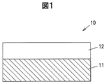
- FIG. 1 is a vertical sectional view of an epitaxial wafer according to the first embodiment.
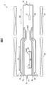
- FIG. 2 is a vertical sectional view of the vapor phase growth apparatus according to the embodiment.
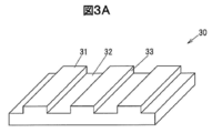
- FIG. 3A is a perspective view showing a part of a main surface of a ⁇ -Ga 2 O 3 single crystal substrate used for evaluation.
- FIG. 3B is a side view showing a part of the main surface of the ⁇ -Ga 2 O 3 single crystal substrate used for the evaluation.
- FIG. 4B is an SEM observation image of a ⁇ -Ga 2 O 3 single crystal substrate in
- FIG. 7 is a graph showing the relationship between the growth rate of the ⁇ -Ga 2 O 3 single crystal by the HVPE method and the plane orientation of the base surface obtained by the evaluation.
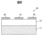
- FIG. 8 is a vertical cross-sectional view of a lateral transistor according to the second embodiment.
- FIG. 1 is a vertical sectional view of an epitaxial wafer 10 according to the first embodiment.
- the epitaxial wafer 10 has a semiconductor substrate 11 and an epitaxial layer 12 formed on the main surface of the semiconductor substrate 11 by epitaxial crystal growth by HVPE (Halide Vapor Phase Epitaxy) method.
- HVPE Hydrode Vapor Phase Epitaxy
- the semiconductor substrate 11 is a substrate made of a ⁇ -Ga 2 O 3 based single crystal.
- the ⁇ -Ga 2 O 3 single crystal is a crystal having a ⁇ -Ga 2 O 3 single crystal or a ⁇ -Ga 2 O 3 single crystal to which an element such as Al or In is added as a mother crystal.
- the composition of ⁇ -Ga 2 O 3 single crystal to which Al and In are added is ⁇ - (Ga x Al y In (1-xy) ) 2 O 3 (0 ⁇ x ⁇ 1, 0 ⁇ y ⁇ 1, 0 ⁇ x + y ⁇ 1).
- the semiconductor substrate 11 may contain a conductivity type impurity such as Si.
- the semiconductor substrate 11 is formed by slicing a bulk crystal of a Ga 2 O 3 single crystal grown by a melt growth method such as an FZ (Floating Zone) method or an EFG (Edge Defined Film Fed Growth) method and polishing the surface. Is formed.
- a melt growth method such as an FZ (Floating Zone) method or an EFG (Edge Defined Film Fed Growth) method and polishing the surface. Is formed.
- the main surface of the semiconductor substrate 11 is a surface parallel to the [010] axis of the ⁇ -Ga 2 O 3 single crystal constituting the semiconductor substrate 11. This is because the growth rate of the epitaxial growth by the HVPE method of the ⁇ -Ga 2 O 3 single crystal layer is extremely low when the plane orientation of the main surface of the ⁇ -Ga 2 O 3 single crystal substrate is (010). This is set based on the discovery of the present inventors.
- the inventors of the present invention have the plane orientation of the main surface of the ⁇ -Ga 2 O 3 single crystal substrate that is not suitable for the growth of the ⁇ -Ga 2 O 3 single crystal layer by this HVPE method and is perpendicular to the (010) plane. It has been found that the growth rate of the epitaxial growth by the HVPE method of the ⁇ -Ga 2 O 3 single crystal layer is high when the surface is a plane parallel to the [010] axis.
- the main surface of the semiconductor substrate 11 has a range of 38 ° or more and 90 ° or less in the direction from the (100) plane to the (101) plane with the [010] axis of the ⁇ -Ga 2 O 3 single crystal as the rotation axis. It is the surface rotated by the angle inside.
- the main surface of the semiconductor substrate 11 is rotated by 68 ⁇ 10 ° in the direction from the (100) plane to the (101) plane with the [010] axis of the ⁇ -Ga 2 O 3 single crystal as the rotation axis. It is the surface.
- ⁇ represents an allowable error.
- 68 ⁇ 10 ° represents an arbitrary angle within a range of 58 ° to 78 °.
- the main surface of the semiconductor substrate 11 is 38 ⁇ 1 °, 53.8 ⁇ in the direction from the (100) plane to the (101) plane with the [010] axis of the ⁇ -Ga 2 O 3 single crystal as the rotation axis. It is also preferable that the surface is rotated by 1 °, 68 ⁇ 1 °, 76.3 ⁇ 1 °, 77.3 ⁇ 1 °, 83 ⁇ 1 °, or 90 ⁇ 1 °.
- the epitaxial layer 12 is made of a ⁇ -Ga 2 O 3 single crystal. Further, the epitaxial layer 12 may contain a conductivity type impurity such as Si.
- FIG. 2 is a vertical sectional view of the vapor phase growth apparatus 2 according to the embodiment.
- the vapor phase growth apparatus 2 is a vapor phase growth apparatus for the HVPE method, and includes a first gas introduction port 21, a second gas introduction port 22, a third gas introduction port 23, and an exhaust port 24. 20 and a first heating unit 26 and a second heating unit 27 that are installed around the reaction chamber 20 and heat a predetermined region in the reaction chamber 20.
- the HVPE method has a higher film formation rate than the PLD method or the like.
- the uniformity of the in-plane distribution of film thickness is high, and a large-diameter film can be grown. For this reason, it is suitable for mass production of crystals.
- the reaction chamber 20 is provided with a reaction vessel 25 containing Ga raw material, a raw material reaction region R1 in which a gallium raw material gas is generated, and a crystal growth region in which the semiconductor substrate 11 is disposed and the epitaxial layer 12 is grown. R2 is included.
- the reaction chamber 20 is made of, for example, quartz glass.
- reaction vessel 25 is, for example, quartz glass, and the Ga raw material accommodated in the reaction vessel 25 is metallic gallium.
- the first heating unit 26 and the second heating unit 27 can heat the raw material reaction region R1 and the crystal growth region R2 of the reaction chamber 20, respectively.
- the first heating unit 26 and the second heating unit 27 are, for example, resistance heating type or radiation heating type heating devices.
- the first gas introduction port 21 uses a Cl-containing gas, which is Cl 2 gas or HCl gas, as a raw material reaction region of the reaction chamber 20 using a carrier gas (N 2 gas, Ar gas, or He gas) that is an inert gas. This is a port for introduction into R1.
- a Cl-containing gas which is Cl 2 gas or HCl gas
- a carrier gas N 2 gas, Ar gas, or He gas
- the second gas introduction port 22 is an oxygen-containing gas such as O 2 gas or H 2 O gas, which is an oxygen source gas, and a chloride-based gas (for example, four gases) for adding a dopant such as Si to the epitaxial layer 12.
- This is a port for introducing silicon chloride or the like into the crystal growth region R2 of the reaction chamber 20 using a carrier gas (N 2 gas, Ar gas, or He gas) that is an inert gas.
- the third gas introduction port 23 is a port for introducing a carrier gas (N 2 gas, Ar gas, or He gas) that is an inert gas into the crystal growth region R 2 of the reaction chamber 20.
- a carrier gas N 2 gas, Ar gas, or He gas
- the raw material reaction region R1 of the reaction chamber 20 is heated using the first heating means 26, and the atmospheric temperature of the raw material reaction region R1 is maintained at a predetermined temperature.
- a Cl-containing gas is introduced from the first gas introduction port 21 using a carrier gas, and the metal gallium and the Cl-containing gas in the reaction vessel 25 are reacted in the raw material reaction region R1 at the above atmospheric temperature. Generates gallium chloride gas.
- the atmospheric temperature in the raw material reaction region R1 is such that the partial pressure of the GaCl gas is the highest among the gallium chloride-based gases generated by the reaction between the metal gallium in the reaction vessel 25 and the Cl-containing gas. Temperature is preferred.
- the gallium chloride-based gas includes GaCl gas, GaCl 2 gas, GaCl 3 gas, (GaCl 3 ) 2 gas, and the like.
- GaCl gas is a gas that can maintain the growth driving force of Ga 2 O 3 crystals up to the highest temperature among the gases contained in the gallium chloride-based gas. High purity, in order to obtain a high quality Ga 2 O 3 crystal, for growth at high growth temperatures are valid, and generates the partial pressure is higher gallium chloride gas of high GaCl gas growth driving force at a high temperature Is preferred for the growth of the epitaxial layer 12.
- Cl 2 gas not containing hydrogen is used as the Cl-containing gas. It is preferable to use it.
- the metal gallium in the reaction vessel 25 is maintained in a state where the atmosphere temperature of the raw material reaction region R1 is maintained at 300 ° C. or higher by the first heating means 26. It is preferable to react a Cl-containing gas.
- the partial pressure ratio of GaCl gas is overwhelmingly high (the equilibrium partial pressure of GaCl gas is 4 orders of magnitude higher than GaCl 2 gas and 8 orders of magnitude higher than GaCl 3 gas). Gases other than GaCl gas hardly contribute to the growth of Ga 2 O 3 crystals.
- the metal in the reaction vessel 25 is maintained in a state where the atmosphere temperature of the raw material reaction region R1 is kept at 1000 ° C. or lower. It is preferable to react gallium with a Cl-containing gas.
- the gallium chloride gas generated in the raw material reaction region R1 and the oxygen-containing gas introduced from the second gas introduction port 22 are mixed, and the semiconductor substrate 11 is mixed with the mixed gas.
- the epitaxial layer 12 is epitaxially grown on the semiconductor substrate 11 by exposure.
- the pressure in the crystal growth region R2 in the furnace containing the reaction chamber 20 is maintained at, for example, 1 atm.
- a source gas of the additive element for example, a chloride-based gas such as silicon tetrachloride (SiCl 4 )
- SiCl 4 silicon tetrachloride
- O 2 gas not containing hydrogen is used as the oxygen-containing gas. It is preferable to use it.
- the ratio of the O 2 gas supply partial pressure to the GaCl gas supply partial pressure in the crystal growth region R2 is 0.
- the epitaxial layer 12 is preferably grown in a state of 5 or more.
- the growth temperature is preferably set to 900 ° C. or higher.
- the epitaxial layer 12 contains, for example, 5 ⁇ 10 16 (atoms / cm 3 ) or less of Cl. This is because the epitaxial layer 12 is formed by the HVPE method using a Cl-containing gas. Normally, when a Ga 2 O 3 single crystal film is formed by a method other than the HVPE method, since a Cl-containing gas is not used, Cl is not contained in the Ga 2 O 3 single crystal film. ⁇ 10 16 (atoms / cm 3 ) does not contain more Cl.
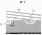
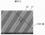
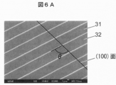
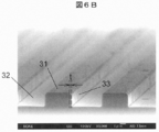
- 3A and 3B are a perspective view and a side view showing a part of the main surface of the ⁇ -Ga 2 O 3 single crystal substrate 30 used for the evaluation.
- the upper surface of the convex portion of the main surface of the ⁇ -Ga 2 O 3 single crystal substrate 30 is defined as a surface 31, the bottom surface of the concave portion is defined as a surface 32, and the side surfaces of the convex portion are defined as surfaces 33 and 34.
- the plane orientation of the planes 31 and 32 is (010).
- the surfaces 33 and 34 are surfaces perpendicular to the surfaces 31 and 32 and are rotated by an angle ⁇ in the direction from the (100) plane to the (101) plane with the [010] axis as the rotation axis. Note that the surface orientation of the surface 34 is further rotated 180 ° from ⁇ , which is equivalent to the surface orientation of the surface 33.
- 4A is an image observed from a direction perpendicular to the principal surface
- FIG. 4B is an image observed obliquely from above.
- 5A is an image observed from a direction perpendicular to the main surface
- FIG. 5B is an image observed from obliquely above.
- 6A is an image observed from a direction perpendicular to the main surface
- FIG. 6B is an image observed from obliquely above.
- the thickness t shown in FIG. 4B, FIG. 5B, and FIG. 6B represents the thickness of the ⁇ -Ga 2 O 3 single crystal grown in the direction perpendicular to the surfaces 33 and.
- FIG. 7 is a graph showing the relationship between the growth rate of the ⁇ -Ga 2 O 3 single crystal by the HVPE method and the plane orientation of the base surface obtained by the evaluation. 7 represents the angle ⁇ of the surface 33, and the vertical axis represents the growth rate of ⁇ -Ga 2 O 3 single crystal in the direction perpendicular to the surfaces 33 and 34 (increase amount per unit time of the thickness t). To express.
- the plot mark ⁇ in FIG. 7 is a measured value by the evaluation method using the ⁇ -Ga 2 O 3 single crystal substrate 30 described above.
- Plot marks ⁇ is, ⁇ -Ga 2 O 3 without using the single crystal substrate 30, the corresponding flat main surface ⁇ -Ga 2 O 3 on a single crystal substrate ⁇ -Ga 2 O 3 single crystal having a plane orientation Is a measured value obtained by observing the growth in the direction perpendicular to the main surface.
- Table 1 below shows the numerical values at each measurement point shown in FIG.
- the growth rate of the ⁇ -Ga 2 O 3 single crystal on the plane parallel to the [010] axis is on the (010) plane in the entire range of 0 ⁇ ⁇ ⁇ 180 °. It is much higher than the growth rate.
- the growth rate of the ⁇ -Ga 2 O 3 single crystal is particularly high in the range of 38 ° ⁇ ⁇ ⁇ 90 °.
- the growth rate of the ⁇ -Ga 2 O 3 single crystal tends to increase as the angle ⁇ approaches 68 °, and the range of 68 ⁇ 10 ° is particularly high. It is estimated that a high growth rate can be obtained.
- the growth rate of the ⁇ -Ga 2 O 3 single crystal is high when the angle is 68 ° ⁇ 1 °, 76.3 ⁇ 1 °, 77.3 ⁇ 1 °, 83 ⁇ 1 °, or 90 ⁇ 1 °.
- the above evaluation was performed by growing a ⁇ -Ga 2 O 3 single crystal on a ⁇ -Ga 2 O 3 single crystal substrate.
- a ⁇ -Ga 2 O 3 single crystal was used as a substrate material and a growth crystal. Similar results can be obtained when evaluation is performed using another ⁇ -Ga 2 O 3 single crystal instead or when evaluation is performed using a ⁇ -Ga 2 O 3 single crystal containing a dopant. .
- the main surface of the semiconductor substrate 11 of the epitaxial wafer 10 is preferably a plane parallel to the [010] axis in order to increase the growth rate of the epitaxial growth of the epitaxial layer 12 by the HVPE method.
- the main surface of the semiconductor substrate 11 is in the range of 38 ° or more and 90 ° or less in the direction from the (100) plane to the (101) plane with the [010] axis of the ⁇ -Ga 2 O 3 single crystal as the rotation axis. It can be said that the surface rotated at an angle of is more preferable.
- the main surface of the semiconductor substrate 11 is a surface rotated by 68 ⁇ 10 ° in the direction from the (100) plane to the (101) plane with the [010] axis of the ⁇ -Ga 2 O 3 single crystal as the rotation axis. It can be said that it is more preferable.
- the main surface of the semiconductor substrate 11 is 38 ⁇ 1 °, 53.8 ⁇ in the direction from the (100) plane to the (101) plane with the [010] axis of the ⁇ -Ga 2 O 3 single crystal as the rotation axis. It can also be said that the surface is preferably rotated by 1 °, 68 ⁇ 1 °, 76.3 ⁇ 1 °, 77.3 ⁇ 1 °, 83 ⁇ 1 °, or 90 ⁇ 1 °.
- the second embodiment is a form of a semiconductor element including the epitaxial wafer 10 according to the first embodiment.
- a lateral transistor having a MESFET (Metal Semiconductor Field Effect Transistor) structure will be described.
- FIG. 8 is a vertical sectional view of a lateral transistor 40 according to the second embodiment.
- the lateral transistor 40 includes an epitaxial layer 12 formed on the semiconductor substrate 11, a gate electrode 41 on the epitaxial layer 12, a source electrode 42, and a drain electrode 43.
- the gate electrode 41 is disposed between the source electrode 42 and the drain electrode 43.
- the source electrode 42 and the drain electrode 43 are in contact with the upper surface of the epitaxial layer 12 (the surface opposite to the surface in contact with the semiconductor substrate 11) to form an ohmic junction. Further, the gate electrode 41 contacts the upper surface of the epitaxial layer 12 to form a Schottky junction, and a depletion layer is formed under the gate electrode 41 in the epitaxial layer 12. Depending on the thickness of the depletion region, the lateral transistor 40 functions as a normally-off transistor or a normally-on transistor.
- the semiconductor substrate 11 is made of a Ga 2 O 3 based crystal containing a p-type dopant such as Mg, Be, Zn, or Fe, and has a high electric resistance.
- the epitaxial layer 12 includes an n-type dopant such as Si or Sn.
- concentration of the n-type dopant in the vicinity of the contact portion with the source electrode 42 and the drain electrode 43 is higher than the concentration of the n-type dopant in other portions.
- the thickness of the epitaxial layer 12 is, for example, 0.1 to 1 ⁇ m.
- the gate electrode 41, the source electrode 42, and the drain electrode 43 are, for example, metals such as Au, Al, Ti, Sn, Ge, In, Ni, Co, Pt, W, Mo, Cr, Cu, and Pb, and these metals. It consists of an alloy containing two or more of these, a conductive compound such as ITO, or a conductive polymer.
- a conductive compound such as ITO, or a conductive polymer.
- a polythiophene derivative PEDOT: poly (3,4) -ethylenedioxythiophene
- PPS polystyrene sulfonic acid
- the gate electrode 41 may have a two-layer structure made of two different metals, for example, Al / Ti, Au / Ni, Au / Co.
- the drain current can be controlled by changing the thickness of the depletion layer under the gate electrode 41 in the epitaxial layer 12 by controlling the bias voltage applied to the gate electrode 41.
- the above-described lateral transistor 40 is an example of a semiconductor element including the epitaxial wafer 10 according to the first embodiment, and in addition, various semiconductor elements can be manufactured using the epitaxial wafer 10.
- a MISFET Metal Insulator Semiconductor Field Field Effect Transistor
- HEMT High Electron Mobility Transistor
- Etc. can be manufactured.
- the type and concentration of the dopant contained in the semiconductor substrate 11 and the epitaxial layer 12 are appropriately set.
- an epitaxial wafer can be efficiently produced by epitaxially growing an epitaxial layer on the semiconductor substrate. Further, since the diffusion of impurities from the semiconductor substrate can be suppressed by growing the epitaxial layer at a high growth rate, this epitaxial wafer has a high-quality epitaxial layer.
- a semiconductor substrate made of ⁇ -Ga 2 O 3 single crystal capable of growing an epitaxial layer made of ⁇ -Ga 2 O 3 single crystal at a high growth rate by the HVPE method, an epitaxial wafer having the semiconductor substrate and the epitaxial layer, and A method for manufacturing the epitaxial wafer is provided.
Abstract
HVPE法によりβ-Ga2O3単結晶からなるエピタキシャル層を高い成長レートで成長させることができるβ-Ga2O3単結晶からなる半導体基板、その半導体基板とエピタキシャル層を有するエピタキシャルウエハ、及びそのエピタキシャルウエハの製造方法を提供する。 一実施の形態として、HVPE法によるエピタキシャル結晶成長用の下地基板として用いられる半導体基板であって、β-Ga2O3系単結晶からなり、β-Ga2O3系単結晶の[010]軸に平行な面を主面とする、半導体基板11を提供する。
Description
本発明は、半導体基板、並びにエピタキシャルウエハ及びその製造方法に関する。
従来、β-Ga2O3系基板上に、MBE(Molecular Beam Epitaxy)法によるエピタキシャル結晶成長によりβ-Ga2O3単結晶膜を形成する技術が知られている(例えば、特許文献1参照)。
特許文献1によれば、β-Ga2O3系基板の主面の面方位を所定の面方位とすることにより、MBE法により、β-Ga2O3単結晶膜を高い成長レートで成長させることができる。
本発明の目的の1つは、HVPE法によりβ-Ga2O3単結晶からなるエピタキシャル層を高い成長レートで成長させることができるβ-Ga2O3単結晶からなる半導体基板、その半導体基板とエピタキシャル層を有するエピタキシャルウエハ、及びそのエピタキシャルウエハの製造方法を提供することにある。
本発明の一態様は、上記目的を達成するために、下記[1]~[4]の半導体基板を提供する。
[1]HVPE法によるエピタキシャル結晶成長用の下地基板として用いられる半導体基板であって、β-Ga2O3系単結晶からなり、β-Ga2O3系単結晶の[010]軸に平行な面を主面とする、半導体基板。
[2]前記主面が、β-Ga2O3系単結晶の[010]軸を回転軸として(100)面から(101)面へ向かう方向に38°以上90°以下の範囲内の角度で回転させた面である、前記[1]に記載の半導体基板。
[3]前記角度が、68±10°である、前記[2]に記載の半導体基板。
[4]前記角度が、38±1°、53.8±1°、68±1°、76.3±1°、77.3±1°、83±1°、又は90±1°である、前記[2]に記載の半導体基板。
また、本発明の他の態様は、上記目的を達成するために、下記[5]のエピタキシャルウエハを提供する。
[5]前記[1]~[4]のいずれか1項に記載の前記半導体基板と、前記半導体基板の前記主面上にHVPE法によるエピタキシャル結晶成長により形成された、β-Ga2O3系単結晶からなるエピタキシャル層と、を有するエピタキシャルウエハ。
また、本発明の他の態様は、上記目的を達成するために、下記[6]~[10]のエピタキシャルウエハの製造方法を提供する。
[6]β-Ga2O3系単結晶からなり、β-Ga2O3系単結晶の[010]軸に平行な面を主面とする半導体基板上に、β-Ga2O3系単結晶からなるエピタキシャル層をHVPE法によるエピタキシャル結晶成長により形成する工程を含む、エピタキシャルウエハの製造方法。
[7]前記エピタキシャル層の成長レートが1.2μm/h以上である、前記[6]に記載のエピタキシャルウエハの製造方法。
[8]前記半導体基板の前記主面が、β-Ga2O3系単結晶の[010]軸を回転軸として(100)面から(101)面へ向かう方向に38°以上90°以下の範囲内の角度で回転させた面である、前記[6]又は[7]に記載のエピタキシャルウエハの製造方法。
[9]前記角度が、68±10°である、前記[8]に記載のエピタキシャルウエハの製造方法。
[10]前記角度が、38±1°、53.8±1°、68±1°、76.3±1°、77.3±1°、83±1°、又は90±1°である、前記[8]に記載のエピタキシャルウエハの製造方法。
本発明によれば、HVPE法によりβ-Ga2O3単結晶からなるエピタキシャル層を高い成長レートで成長させることができるβ-Ga2O3単結晶からなる半導体基板、その半導体基板とエピタキシャル層を有するエピタキシャルウエハ、及びそのエピタキシャルウエハの製造方法を提供することができる。
〔第1の実施の形態〕
(結晶積層構造体の構成)
図1は、第1の実施の形態に係るエピタキシャルウエハ10の垂直断面図である。エピタキシャルウエハ10は、半導体基板11と、半導体基板11の主面上にHVPE(Halide Vapor Phase Epitaxy)法によるエピタキシャル結晶成長により形成されたエピタキシャル層12を有する。
(結晶積層構造体の構成)
図1は、第1の実施の形態に係るエピタキシャルウエハ10の垂直断面図である。エピタキシャルウエハ10は、半導体基板11と、半導体基板11の主面上にHVPE(Halide Vapor Phase Epitaxy)法によるエピタキシャル結晶成長により形成されたエピタキシャル層12を有する。
半導体基板11は、β-Ga2O3系単結晶からなる基板である。ここで、β-Ga2O3系単結晶とは、β-Ga2O3単結晶、又は、Al、In等の元素が添加されたβ-Ga2O3単結晶を母結晶とする結晶をいう。例えば、Al及びInが添加されたβ-Ga2O3単結晶の組成は、β-(GaxAlyIn(1-x-y))2O3(0<x≦1、0≦y≦1、0<x+y≦1)で表される。Alを添加した場合にはβ-Ga2O3単結晶のバンドギャップが広がり、Inを添加した場合にはバンドギャップが狭くなる。また、半導体基板11は、Si等の導電型不純物を含んでもよい。
半導体基板11は、例えば、FZ(Floating Zone)法やEFG(Edge Defined Film Fed Growth)法等の融液成長法により育成したGa2O3系単結晶のバルク結晶をスライスし、表面を研磨することにより形成される。
半導体基板11の主面は、半導体基板11を構成するβ-Ga2O3系単結晶の[010]軸に平行な面である。これは、β-Ga2O3系単結晶基板の主面の面方位が(010)であるときに、β-Ga2O3系単結晶層のHVPE法によるエピタキシャル成長の成長レートが極端に低くなるという本発明者らの発見に基づいて設定されたものである。
本発明者らは、β-Ga2O3系単結晶基板の主面の面方位が、このHVPE法によるβ-Ga2O3系単結晶層の成長に適さない(010)面に垂直な面、すなわち[010]軸に平行な面であるときに、β-Ga2O3系単結晶層のHVPE法によるエピタキシャル成長の成長レートが高くなることを見出した。
好ましくは、半導体基板11の主面は、β-Ga2O3系単結晶の[010]軸を回転軸として(100)面から(101)面へ向かう方向に38°以上90°以下の範囲内の角度で回転させた面である。
より好ましくは、半導体基板11の主面は、β-Ga2O3系単結晶の[010]軸を回転軸として(100)面から(101)面へ向かう方向に、68±10°回転させた面である。ここで、「±」は許容誤差を表し、例えば、68±10°は、58°以上78°以下の範囲内の任意の角度を表す。
また、半導体基板11の主面は、β-Ga2O3系単結晶の[010]軸を回転軸として(100)面から(101)面へ向かう方向に38±1°、53.8±1°、68±1°、76.3±1°、77.3±1°、83±1°、又は90±1°回転させた面であることも好ましい。
エピタキシャル層12は、半導体基板11と同様に、β-Ga2O3系単結晶からなる。また、エピタキシャル層12は、Si等の導電型不純物を含んでもよい。
(気相成長装置の構造)
以下に、本実施の形態に係るエピタキシャル層12の成長に用いる気相成長装置の構造の一例について説明する。
以下に、本実施の形態に係るエピタキシャル層12の成長に用いる気相成長装置の構造の一例について説明する。
図2は、実施の形態に係る気相成長装置2の垂直断面図である。気相成長装置2は、HVPE法用の気相成長装置であり、第1のガス導入ポート21、第2のガス導入ポート22、第3のガス導入ポート23、及び排気ポート24を有する反応チャンバー20と、反応チャンバー20の周囲に設置され、反応チャンバー20内の所定の領域を加熱する第1の加熱手段26及び第2の加熱手段27を有する。
HVPE法は、PLD法等と比較して、成膜レートが高い。また、膜厚の面内分布の均一性が高く、大口径の膜を成長させることができる。このため、結晶の大量生産に適している。
反応チャンバー20は、Ga原料が収容された反応容器25が配置され、ガリウムの原料ガスが生成される原料反応領域R1と、半導体基板11が配置され、エピタキシャル層12の成長が行われる結晶成長領域R2を有する。反応チャンバー20は、例えば、石英ガラスからなる。
ここで、反応容器25は、例えば、石英ガラスであり、反応容器25に収容されるGa原料は金属ガリウムである。
第1の加熱手段26と第2の加熱手段27は、反応チャンバー20の原料反応領域R1と結晶成長領域R2をそれぞれ加熱することができる。第1の加熱手段26及び第2の加熱手段27は、例えば、抵抗加熱式や輻射加熱式の加熱装置である。
第1のガス導入ポート21は、Cl2ガス又はHClガスであるCl含有ガスを、不活性ガスであるキャリアガス(N2ガス、Arガス又はHeガス)を用いて反応チャンバー20の原料反応領域R1内に導入するためのポートである。
第2のガス導入ポート22は、酸素の原料ガスであるO2ガスやH2Oガス等の酸素含有ガス及びエピタキシャル層12にSi等のドーパントを添加するための塩化物系ガス(例えば、四塩化ケイ素等)を、不活性ガスであるキャリアガス(N2ガス、Arガス又はHeガス)を用いて反応チャンバー20の結晶成長領域R2へ導入するためのポートである。
第3のガス導入ポート23は、不活性ガスであるキャリアガス(N2ガス、Arガス又はHeガス)を反応チャンバー20の結晶成長領域R2へ導入するためのポートである。
(エピタキシャル層の成長)
以下に、本実施の形態に係るエピタキシャル層12の成長工程の一例について説明する。
以下に、本実施の形態に係るエピタキシャル層12の成長工程の一例について説明する。
まず、第1の加熱手段26を用いて反応チャンバー20の原料反応領域R1を加熱し、原料反応領域R1の雰囲気温度を所定の温度に保つ。
次に、第1のガス導入ポート21からCl含有ガスを、キャリアガスを用いて導入し、原料反応領域R1において、上記の雰囲気温度下で反応容器25内の金属ガリウムとCl含有ガスを反応させ、塩化ガリウム系ガスを生成する。
このとき、上記の原料反応領域R1内の雰囲気温度は、反応容器25内の金属ガリウムとCl含有ガスの反応により生成される塩化ガリウム系ガスのうち、GaClガスの分圧が最も高くなるような温度であることが好ましい。ここで、塩化ガリウム系ガスには、GaClガス、GaCl2ガス、GaCl3ガス、(GaCl3)2ガス等が含まれる。
GaClガスは、塩化ガリウム系ガスに含まれるガスのうち、Ga2O3結晶の成長駆動力を最も高い温度まで保つことのできるガスである。高純度、高品質のGa2O3結晶を得るためには、高い成長温度での成長が有効であるため、高温において成長駆動力の高いGaClガスの分圧が高い塩化ガリウム系ガスを生成することが、エピタキシャル層12の成長のために好ましい。
なお、エピタキシャル層12を成長させる際の雰囲気に水素が含まれていると、エピタキシャル層12の表面の平坦性及び結晶成長駆動力が低下するため、水素を含まないCl2ガスをCl含有ガスとして用いることが好ましい。
また、塩化ガリウム系ガスのうちのGaClガスの分圧比を高くするため、第1の加熱手段26により原料反応領域R1の雰囲気温度を300℃以上に保持した状態で反応容器25内の金属ガリウムとCl含有ガスを反応させることが好ましい。
また、例えば、850℃以上の雰囲気温度下では、GaClガスの分圧比が圧倒的に高くなる(GaClガスの平衡分圧がGaCl2ガスより4桁大きく、GaCl3ガスより8桁大きい)ため、GaClガス以外のガスはGa2O3結晶の成長にほとんど寄与しない。
なお、第1の加熱手段26の寿命や、石英ガラス等からなる反応チャンバー20の耐熱性を考慮して、原料反応領域R1の雰囲気温度を1000℃以下に保持した状態で反応容器25内の金属ガリウムとCl含有ガスを反応させることが好ましい。
次に、結晶成長領域R2において、原料反応領域R1で生成された塩化ガリウム系ガスと、第2のガス導入ポート22から導入された酸素含有ガスとを混合させ、その混合ガスに半導体基板11を曝し、半導体基板11上にエピタキシャル層12をエピタキシャル成長させる。このとき、反応チャンバー20を収容する炉内の結晶成長領域R2における圧力を、例えば、1atmに保つ。
ここで、Si、Al等の添加元素を含むエピタキシャル層12を形成する場合には、ガス導入ポート22より、添加元素の原料ガス(例えば、四塩化ケイ素(SiCl4)等の塩化物系ガス)も塩化ガリウム系ガス及び酸素含有ガスに併せて結晶成長領域R2に導入する。
なお、エピタキシャル層12を成長させる際の雰囲気に水素が含まれていると、エピタキシャル層12の表面の平坦性及び結晶成長駆動力が低下するため、酸素含有ガスとして水素を含まないO2ガスを用いることが好ましい。
また、GaClガスの平衡分圧の低下を抑え、エピタキシャル層12を効率的に成長させるためには、結晶成長領域R2におけるO2ガスの供給分圧のGaClガスの供給分圧に対する比が0.5以上である状態でエピタキシャル層12を成長させることが好ましい。
また、高品質のエピタキシャル層12を成長させるために、成長温度を900℃以上にすることが好ましい。
なお、エピタキシャル層12は、例えば、5×10¹⁶(atoms/cm3)以下のClを含む。これは、エピタキシャル層12がCl含有ガスを用いるHVPE法により形成されることに起因する。通常、HVPE法以外の方法によりGa2O3単結晶膜を形成する場合には、Cl含有ガスを用いないため、Ga2O3単結晶膜中にClが含まれることはなく、少なくとも、1×1016(atoms/cm3)以上のClが含まれることはない。
(半導体基板の主面の面方位)
以下に、半導体基板11の主面の面方位と、エピタキシャル層12の成長レートの関係の評価結果を示す。この評価は、(010)面である主面にラインアンドスペースパターンの凹凸が形成されたβ-Ga2O3単結晶基板を用いて行った。
以下に、半導体基板11の主面の面方位と、エピタキシャル層12の成長レートの関係の評価結果を示す。この評価は、(010)面である主面にラインアンドスペースパターンの凹凸が形成されたβ-Ga2O3単結晶基板を用いて行った。
図3A、図3Bは、評価に用いられたβ-Ga2O3単結晶基板30の主面の一部を表す斜視図と側面図である。β-Ga2O3単結晶基板30の主面の凸部の上面を面31、凹部の底面を面32、凸部の側面を面33、34とする。
面31、32の面方位は(010)である。面33、34は面31、32に垂直な面であり、[010]軸を回転軸として(100)面から(101)面へ向かう方向へ角度θだけ回転させた面である。なお、面34の面方位はθからさらに180°回転しており、面33の面方位と等価である。
HVPE法によりβ-Ga2O3単結晶基板30上にβ-Ga2O3単結晶をエピタキシャル成長させ、面33、34に垂直な方向のβ-Ga2O3単結晶の成長を観察することにより、[010]軸に平行な面の面方位とβ-Ga2O3単結晶の成長レートとの関係を評価した。
図4A、図4Bは、θ=38°であるβ-Ga2O3単結晶基板30のSEM(Scanning Electron Microscope)観察画像である。図4Aは主面に垂直な方向から観察した画像であり、図4Bは斜め上方から観察した画像である。
図5A、図5Bは、θ=68°であるβ-Ga2O3単結晶基板30のSEM観察画像である。図5Aは主面に垂直な方向から観察した画像であり、図5Bは斜め上方から観察した画像である。
図6A、図6Bは、θ=98°であるβ-Ga2O3単結晶基板30のSEM観察画像である。図6Aは主面に垂直な方向から観察した画像であり、図6Bは斜め上方から観察した画像である。
図4B、図5B、図6Bに示される厚さtは、面33、34に垂直な方向へ成長したβ-Ga2O3単結晶の厚さを表す。
図7は、評価により得られた、HVPE法によるβ-Ga2O3単結晶の成長レートと下地面の面方位との関係を表すグラフである。図7の横軸は面33の角度θを表し、縦軸は面33、34に垂直な方向のβ-Ga2O3単結晶の成長レート(厚さtの単位時間あたりの増加量)を表す。
図7中の点線は(010)面、(001)面、(-101)面、(-201)面に対応する角度θを表しており、例えば、θ=53.8°のときに面33が(101)面に一致しており、面34は(-10-1)面に一致することを表している。
図7中のプロットマーク◆は、上記のβ-Ga2O3単結晶基板30を用いた評価方法による測定値である。プロットマーク◇は、β-Ga2O3単結晶基板30を用いずに、対応する面方位の平坦な主面を有するβ-Ga2O3単結晶基板上にβ-Ga2O3単結晶を成長させ、主面に垂直な方向の成長を観察して得た測定値である。
以下の表1に、図7に示される各測定点の数値を表す。

なお、(010)面を主面とするβ-Ga2O3単結晶基板上にβ-Ga2O3単結晶を同じ成長条件で成長させたところ、主面に垂直な方向のβ-Ga2O3単結晶の成長レートは、0.3μm/hであった。
図7、表1に示されるように、[010]軸に平行な面上のβ-Ga2O3単結晶の成長レートは、0≦θ≦180°の全範囲において、(010)面上の成長レートよりも格段に高い。例えば、図7、表1に示される[010]軸に平行な面上のβ-Ga2O3単結晶の成長レートのうちの、最も低い成長レートである1.20μm/h(θ=126.2)であっても、(010)面上の成長レートである0.3μm/hの4倍である。このことから、β-Ga2O3単結晶基板の主面が[010]軸に平行な面であるときに、β-Ga2O3単結晶のHVPE法によるエピタキシャル成長の成長レートが高くなるといえる。
また、図7、表1に示されるように、38°≦θ≦90°の範囲において、特にβ-Ga2O3単結晶の成長レートが高い。
さらに、38°≦θ≦90°の範囲においては、角度θが68°付近に近づくほどβ-Ga2O3単結晶の成長レートが高くなる傾向がみられ、68±10°の範囲で特に高い成長レートが得られることが推測される。
また、β-Ga2O3単結晶基板の主面の傾きがおよそ±1°以内であれば、成長レートは大きく変化しないため、実測値から、θ=38±1°、53.8±1°、68±1°、76.3±1°、77.3±1°、83±1°、又は90±1°のときにβ-Ga2O3単結晶の成長レートが高くなるといえる。
以上の評価は、β-Ga2O3単結晶基板上にβ-Ga2O3単結晶を成長させることにより行われたが、基板の材料及び成長結晶としてβ-Ga2O3単結晶の代わりに他のβ-Ga2O3系単結晶を用いて評価を行う場合や、ドーパントを含むβ-Ga2O3系単結晶を用いて評価を行う場合にも、同様の結果が得られる。
このため、エピタキシャル層12のHVPE法によるエピタキシャル成長の成長レートを高くするためには、エピタキシャルウエハ10の半導体基板11の主面が[010]軸に平行な面であることが好ましいといえる。
また、半導体基板11の主面が、β-Ga2O3系単結晶の[010]軸を回転軸として(100)面から(101)面へ向かう方向に38°以上90°以下の範囲内の角度で回転させた面であることがより好ましいといえる。
さらに、半導体基板11の主面が、β-Ga2O3系単結晶の[010]軸を回転軸として(100)面から(101)面へ向かう方向に、68±10°回転させた面であることがより好ましいといえる。
また、半導体基板11の主面は、β-Ga2O3系単結晶の[010]軸を回転軸として(100)面から(101)面へ向かう方向に38±1°、53.8±1°、68±1°、76.3±1°、77.3±1°、83±1°、又は90±1°回転させた面であることも好ましいといえる。
〔第2の実施の形態〕
第2の実施の形態は、第1の実施の形態に係るエピタキシャルウエハ10を含む半導体素子についての形態である。この半導体素子の一例として、いかに、MESFET(Metal Semiconductor Field Effect Transistor)構造を有する横型トランジスタについて説明する。
第2の実施の形態は、第1の実施の形態に係るエピタキシャルウエハ10を含む半導体素子についての形態である。この半導体素子の一例として、いかに、MESFET(Metal Semiconductor Field Effect Transistor)構造を有する横型トランジスタについて説明する。
(半導体素子の構造)
図8は、第2の実施の形態に係る横型トランジスタ40の垂直断面図である。横型トランジスタ40は、半導体基板11上に形成されたエピタキシャル層12と、エピタキシャル層12上のゲート電極41、ソース電極42、及びドレイン電極43を含む。ゲート電極41は、ソース電極42とドレイン電極43との間に配置される。
図8は、第2の実施の形態に係る横型トランジスタ40の垂直断面図である。横型トランジスタ40は、半導体基板11上に形成されたエピタキシャル層12と、エピタキシャル層12上のゲート電極41、ソース電極42、及びドレイン電極43を含む。ゲート電極41は、ソース電極42とドレイン電極43との間に配置される。
ソース電極42及びドレイン電極43は、エピタキシャル層12の上面(半導体基板11に接している面の反対側の面)に接触してオーミック接合を形成する。また、ゲート電極41はエピタキシャル層12の上面に接触してショットキー接合を形成し、エピタキシャル層12中のゲート電極41下に空乏層が形成される。この空乏領域の厚さにより、横型トランジスタ40は、ノーマリーオフ型のトランジスタ又はノーマリーオン型のトランジスタとして機能する。
半導体基板11は、Mg、Be、Zn、Fe等のp型ドーパントを含むGa2O3系結晶からなり、高い電気抵抗を有する。
エピタキシャル層12は、Si、Sn等のn型ドーパントを含む。ソース電極42及びドレイン電極43との接触部付近におけるn型ドーパントの濃度は、他の部分におけるn型ドーパントの濃度よりも高い。エピタキシャル層12の厚さは、例えば、0.1~1μmである。
ゲート電極41、ソース電極42、及びドレイン電極43は、例えば、Au、Al、Ti、Sn、Ge、In、Ni、Co、Pt、W、Mo、Cr、Cu、Pb等の金属、これらの金属のうちの2つ以上を含む合金、ITO等の導電性化合物、又は導電性ポリマーからなる。導電性ポリマーとしては、ポリチオフェン誘導体(PEDOT:ポリ(3,4)-エチレンジオキシチオフェン)にポリスチレンスルホン酸(PSS)をドーピングしたものや、ポリピロール誘導体にTCNAをドーピングしたもの等が用いられる。また、ゲート電極41は、異なる2つの金属からなる2層構造、例えばAl/Ti、Au/Ni、Au/Co、を有してもよい。
横型トランジスタ40においては、ゲート電極41に印加するバイアス電圧を制御することにより、エピタキシャル層12内のゲート電極41下の空乏層の厚さを変化させ、ドレイン電流を制御することができる。
上記の横型トランジスタ40は、第1の実施の形態に係るエピタキシャルウエハ10を含む半導体素子の一例であり、その他にも、エピタキシャルウエハ10を用いて様々な半導体素子を製造することができる。
例えば、エピタキシャル層12をチャネル層として用いるMISFET(Metal Insulator Semiconductor Field Effect Transistor)やHEMT(High Electron Mobility Transistor)、半導体基板11とエピタキシャル層12にオーミック電極とショットキー電極がそれぞれ接続されるショットキーダイオード等を製造することができる。製造する半導体素子の種類によって、半導体基板11とエピタキシャル層12に含まれるドーパントの種類や濃度を適宜設定する。
(実施の形態の効果)
上記実施の形態によれば、HVPE法によりβ-Ga2O3単結晶からなるエピタキシャル層を高い成長レートで成長させることができるβ-Ga2O3単結晶からなる半導体基板を提供することができる。
上記実施の形態によれば、HVPE法によりβ-Ga2O3単結晶からなるエピタキシャル層を高い成長レートで成長させることができるβ-Ga2O3単結晶からなる半導体基板を提供することができる。
また、その半導体基板上にエピタキシャル層をエピタキシャル成長させることにより、効率よくエピタキシャルウエハを製造することができる。また、エピタキシャル層を高い成長レートで成長させることにより、半導体基板からの不純物の拡散を抑制することができるため、このエピタキシャルウエハは、高品質のエピタキシャル層を有する。
さらに、そのエピタキシャルウエハを用いることにより、効率よく高品質な半導体素子を製造することができる。
以上、本発明の実施の形態を説明したが、本発明は、上記実施の形態に限定されず、発明の主旨を逸脱しない範囲内において種々変形実施が可能である。
また、上記に記載した実施の形態は特許請求の範囲に係る発明を限定するものではない。また、実施の形態の中で説明した特徴の組合せの全てが発明の課題を解決するための手段に必須であるとは限らない点に留意すべきである。
HVPE法によりβ-Ga2O3単結晶からなるエピタキシャル層を高い成長レートで成長させることができるβ-Ga2O3単結晶からなる半導体基板、その半導体基板とエピタキシャル層を有するエピタキシャルウエハ、及びそのエピタキシャルウエハの製造方法を提供する。
10…エピタキシャルウエハ、 11…半導体基板、 12…エピタキシャル層
Claims (10)
- HVPE法によるエピタキシャル結晶成長用の下地基板として用いられる半導体基板であって、
β-Ga2O3系単結晶からなり、β-Ga2O3系単結晶の[010]軸に平行な面を主面とする、
半導体基板。 - 前記主面が、β-Ga2O3系単結晶の[010]軸を回転軸として(100)面から(101)面へ向かう方向に38°以上90°以下の範囲内の角度で回転させた面である、
請求項1に記載の半導体基板。 - 前記角度が、68±10°である、
請求項2に記載の半導体基板。 - 前記角度が、38±1°、53.8±1°、68±1°、76.3±1°、77.3±1°、83±1°、又は90±1°である、
請求項2に記載の半導体基板。 - 請求項1~4のいずれか1項に記載の前記半導体基板と、
前記半導体基板の前記主面上にHVPE法によるエピタキシャル結晶成長により形成された、β-Ga2O3系単結晶からなるエピタキシャル層と、
を有するエピタキシャルウエハ。 - β-Ga2O3系単結晶からなり、β-Ga2O3系単結晶の[010]軸に平行な面を主面とする半導体基板上に、β-Ga2O3系単結晶からなるエピタキシャル層をHVPE法によるエピタキシャル結晶成長により形成する工程を含む、
エピタキシャルウエハの製造方法。 - 前記エピタキシャル層の成長レートが1.2μm/h以上である、
請求項6に記載のエピタキシャルウエハの製造方法。 - 前記半導体基板の前記主面が、β-Ga2O3系単結晶の[010]軸を回転軸として(100)面から(101)面へ向かう方向に38°以上90°以下の範囲内の角度で回転させた面である、
請求項6又は7に記載のエピタキシャルウエハの製造方法。 - 前記角度が、68±10°である、
請求項8に記載のエピタキシャルウエハの製造方法。 - 前記角度が、38±1°、53.8±1°、68±1°、76.3±1°、77.3±1°、83±1°、又は90±1°である、
請求項8に記載のエピタキシャルウエハの製造方法。
Priority Applications (3)
| Application Number | Priority Date | Filing Date | Title |
|---|---|---|---|
| EP15789328.0A EP3141635B1 (en) | 2014-05-09 | 2015-05-11 | Semiconductor substrate, epitaxial wafer, and method for manufacturing epitaxial wafer |
| CN201580024046.XA CN106471163B (zh) | 2014-05-09 | 2015-05-11 | 半导体衬底、外延片及其制造方法 |
| US15/309,956 US10676841B2 (en) | 2014-05-09 | 2015-05-11 | Semiconductor substrate, epitaxial wafer, and method for manufacturing epitaxial wafer |
Applications Claiming Priority (2)
| Application Number | Priority Date | Filing Date | Title |
|---|---|---|---|
| JP2014097751A JP6253150B2 (ja) | 2014-05-09 | 2014-05-09 | エピタキシャルウエハ及びその製造方法 |
| JP2014-097751 | 2014-05-09 |
Publications (1)
| Publication Number | Publication Date |
|---|---|
| WO2015170774A1 true WO2015170774A1 (ja) | 2015-11-12 |
Family
ID=54392621
Family Applications (1)
| Application Number | Title | Priority Date | Filing Date |
|---|---|---|---|
| PCT/JP2015/063523 WO2015170774A1 (ja) | 2014-05-09 | 2015-05-11 | 半導体基板、並びにエピタキシャルウエハ及びその製造方法 |
Country Status (6)
| Country | Link |
|---|---|
| US (1) | US10676841B2 (ja) |
| EP (1) | EP3141635B1 (ja) |
| JP (1) | JP6253150B2 (ja) |
| CN (1) | CN106471163B (ja) |
| TW (1) | TWI721945B (ja) |
| WO (1) | WO2015170774A1 (ja) |
Cited By (1)
| Publication number | Priority date | Publication date | Assignee | Title |
|---|---|---|---|---|
| CN108368641A (zh) * | 2015-12-16 | 2018-08-03 | 株式会社田村制作所 | 半导体基板、以及外延晶片及其制造方法 |
Families Citing this family (4)
| Publication number | Priority date | Publication date | Assignee | Title |
|---|---|---|---|---|
| JP5984069B2 (ja) * | 2013-09-30 | 2016-09-06 | 株式会社タムラ製作所 | β−Ga2O3系単結晶膜の成長方法、及び結晶積層構造体 |
| CN113394079A (zh) * | 2021-06-18 | 2021-09-14 | 中国电子科技集团公司第四十六研究所 | 一种采用卤化物气相外延法生长氧化镓外延层的方法 |
| WO2023032140A1 (ja) * | 2021-09-03 | 2023-03-09 | 三菱電機株式会社 | 結晶積層構造体、半導体装置、及び、結晶積層構造体の製造方法 |
| WO2024048710A1 (ja) * | 2022-08-31 | 2024-03-07 | 株式会社Flosfia | 結晶膜および結晶膜の製造方法 |
Citations (4)
| Publication number | Priority date | Publication date | Assignee | Title |
|---|---|---|---|---|
| WO2013035464A1 (ja) * | 2011-09-08 | 2013-03-14 | 株式会社タムラ製作所 | 結晶積層構造体及びその製造方法 |
| JP2013227202A (ja) * | 2012-03-30 | 2013-11-07 | Mitsubishi Chemicals Corp | 周期表第13族金属窒化物半導体結晶の製造方法、および、当該製造方法によって得られた周期表第13族金属窒化物半導体結晶を用いた半導体発光デバイス |
| JP2013229554A (ja) * | 2012-03-30 | 2013-11-07 | Mitsubishi Chemicals Corp | 周期表第13族金属窒化物半導体結晶の製造方法、それに用いるノズルおよび製造装置 |
| JP2015091740A (ja) * | 2013-09-30 | 2015-05-14 | 株式会社タムラ製作所 | β−Ga2O3系単結晶膜の成長方法、及び結晶積層構造体 |
Family Cites Families (10)
| Publication number | Priority date | Publication date | Assignee | Title |
|---|---|---|---|---|
| US7008839B2 (en) * | 2002-03-08 | 2006-03-07 | Matsushita Electric Industrial Co., Ltd. | Method for manufacturing semiconductor thin film |
| JP4680762B2 (ja) | 2005-12-14 | 2011-05-11 | 株式会社光波 | 発光素子及びその製造方法 |
| US20070134833A1 (en) | 2005-12-14 | 2007-06-14 | Toyoda Gosei Co., Ltd. | Semiconductor element and method of making same |
| GB2436398B (en) * | 2006-03-23 | 2011-08-24 | Univ Bath | Growth method using nanostructure compliant layers and HVPE for producing high quality compound semiconductor materials |
| KR100969127B1 (ko) * | 2010-02-18 | 2010-07-09 | 엘지이노텍 주식회사 | 발광 소자, 발광 소자 제조방법 및 발광 소자 패키지 |
| CN101967680B (zh) * | 2010-11-04 | 2012-02-01 | 山东大学 | 一种在氧化镁衬底上制备单斜晶型氧化镓单晶薄膜的方法 |
| WO2013035842A1 (ja) * | 2011-09-08 | 2013-03-14 | 株式会社タムラ製作所 | Ga2O3系半導体素子 |
| US9142623B2 (en) | 2011-09-08 | 2015-09-22 | Tamura Corporation | Substrate for epitaxial growth, and crystal laminate structure |
| EP2765610B1 (en) * | 2011-09-08 | 2018-12-26 | Tamura Corporation | Ga2o3 semiconductor element |
| CN103489967B (zh) * | 2013-09-05 | 2016-07-13 | 大连理工大学 | 一种氧化镓外延膜的制备方法及氧化镓外延膜 |
-
2014
- 2014-05-09 JP JP2014097751A patent/JP6253150B2/ja active Active
-
2015
- 2015-05-11 WO PCT/JP2015/063523 patent/WO2015170774A1/ja active Application Filing
- 2015-05-11 US US15/309,956 patent/US10676841B2/en active Active
- 2015-05-11 TW TW104114927A patent/TWI721945B/zh active
- 2015-05-11 EP EP15789328.0A patent/EP3141635B1/en active Active
- 2015-05-11 CN CN201580024046.XA patent/CN106471163B/zh active Active
Patent Citations (4)
| Publication number | Priority date | Publication date | Assignee | Title |
|---|---|---|---|---|
| WO2013035464A1 (ja) * | 2011-09-08 | 2013-03-14 | 株式会社タムラ製作所 | 結晶積層構造体及びその製造方法 |
| JP2013227202A (ja) * | 2012-03-30 | 2013-11-07 | Mitsubishi Chemicals Corp | 周期表第13族金属窒化物半導体結晶の製造方法、および、当該製造方法によって得られた周期表第13族金属窒化物半導体結晶を用いた半導体発光デバイス |
| JP2013229554A (ja) * | 2012-03-30 | 2013-11-07 | Mitsubishi Chemicals Corp | 周期表第13族金属窒化物半導体結晶の製造方法、それに用いるノズルおよび製造装置 |
| JP2015091740A (ja) * | 2013-09-30 | 2015-05-14 | 株式会社タムラ製作所 | β−Ga2O3系単結晶膜の成長方法、及び結晶積層構造体 |
Non-Patent Citations (1)
| Title |
|---|
| See also references of EP3141635A4 * |
Cited By (4)
| Publication number | Priority date | Publication date | Assignee | Title |
|---|---|---|---|---|
| CN108368641A (zh) * | 2015-12-16 | 2018-08-03 | 株式会社田村制作所 | 半导体基板、以及外延晶片及其制造方法 |
| EP3396030A4 (en) * | 2015-12-16 | 2019-07-24 | Tamura Corporation | SEMICONDUCTOR SUBSTRATE AND EPITACTIC WAFER AND METHOD FOR THE PRODUCTION THEREOF |
| US10985016B2 (en) | 2015-12-16 | 2021-04-20 | Tamura Corporation | Semiconductor substrate, and epitaxial wafer and method for producing same |
| CN108368641B (zh) * | 2015-12-16 | 2021-04-27 | 株式会社田村制作所 | 半导体基板、以及外延晶片及其制造方法 |
Also Published As
| Publication number | Publication date |
|---|---|
| JP6253150B2 (ja) | 2017-12-27 |
| EP3141635A1 (en) | 2017-03-15 |
| TW201606114A (zh) | 2016-02-16 |
| JP2015214448A (ja) | 2015-12-03 |
| EP3141635A4 (en) | 2018-01-10 |
| CN106471163B (zh) | 2020-03-24 |
| US10676841B2 (en) | 2020-06-09 |
| TWI721945B (zh) | 2021-03-21 |
| US20170145590A1 (en) | 2017-05-25 |
| CN106471163A (zh) | 2017-03-01 |
| EP3141635B1 (en) | 2023-05-03 |
Similar Documents
| Publication | Publication Date | Title |
|---|---|---|
| JP5984069B2 (ja) | β−Ga2O3系単結晶膜の成長方法、及び結晶積層構造体 | |
| JP5018423B2 (ja) | Iii族窒化物半導体結晶基板および半導体デバイス | |
| JP6744523B2 (ja) | 半導体基板、並びにエピタキシャルウエハ及びその製造方法 | |
| WO2015170774A1 (ja) | 半導体基板、並びにエピタキシャルウエハ及びその製造方法 | |
| WO2016152335A1 (ja) | 結晶積層構造体 | |
| US10199512B2 (en) | High voltage withstand Ga2O3-based single crystal schottky barrier diode | |
| JP2006111478A (ja) | 炭化珪素単結晶インゴット、炭化珪素単結晶ウェハ及びその製造方法 | |
| JP5135708B2 (ja) | Iii族窒化物系電子デバイスおよびエピタキシャル基板 | |
| US9418840B2 (en) | Silicon carbide semiconductor device manufacturing method and silicon carbide semiconductor device | |
| TW202100827A (zh) | GaN結晶及基板 | |
| JP2006179861A (ja) | 半導体エピタキシャルウェハ及び電界効果トランジスタ | |
| US20120104557A1 (en) | Method for manufacturing a group III nitride crystal, method for manufacturing a group III nitride template, group III nitride crystal and group III nitride template | |
| JP6875708B2 (ja) | 結晶積層構造体、及びそれを製造する方法 | |
| JP5641029B2 (ja) | Iii族窒化物系電子デバイス | |
| US11982016B2 (en) | Method for growing beta-Ga2O3-based single crystal film, and crystalline layered structure | |
| WO2023058493A1 (ja) | エピタキシャル層のキャリア濃度を均一化する方法及びそれらの方法により作製された構造 |
Legal Events
| Date | Code | Title | Description |
|---|---|---|---|
| 121 | Ep: the epo has been informed by wipo that ep was designated in this application |
Ref document number: 15789328 Country of ref document: EP Kind code of ref document: A1 |
|
| NENP | Non-entry into the national phase |
Ref country code: DE |
|
| WWE | Wipo information: entry into national phase |
Ref document number: 15309956 Country of ref document: US |
|
| REEP | Request for entry into the european phase |
Ref document number: 2015789328 Country of ref document: EP |
|
| WWE | Wipo information: entry into national phase |
Ref document number: 2015789328 Country of ref document: EP |