WO2015170774A1 - 半導体基板、並びにエピタキシャルウエハ及びその製造方法 - Google Patents
半導体基板、並びにエピタキシャルウエハ及びその製造方法 Download PDFInfo
- Publication number
- WO2015170774A1 WO2015170774A1 PCT/JP2015/063523 JP2015063523W WO2015170774A1 WO 2015170774 A1 WO2015170774 A1 WO 2015170774A1 JP 2015063523 W JP2015063523 W JP 2015063523W WO 2015170774 A1 WO2015170774 A1 WO 2015170774A1
- Authority
- WO
- WIPO (PCT)
- Prior art keywords
- single crystal
- semiconductor substrate
- gas
- epitaxial
- plane
- Prior art date
- Legal status (The legal status is an assumption and is not a legal conclusion. Google has not performed a legal analysis and makes no representation as to the accuracy of the status listed.)
- Ceased
Links
Images


Classifications
-
- C—CHEMISTRY; METALLURGY
- C30—CRYSTAL GROWTH
- C30B—SINGLE-CRYSTAL GROWTH; UNIDIRECTIONAL SOLIDIFICATION OF EUTECTIC MATERIAL OR UNIDIRECTIONAL DEMIXING OF EUTECTOID MATERIAL; REFINING BY ZONE-MELTING OF MATERIAL; PRODUCTION OF A HOMOGENEOUS POLYCRYSTALLINE MATERIAL WITH DEFINED STRUCTURE; SINGLE CRYSTALS OR HOMOGENEOUS POLYCRYSTALLINE MATERIAL WITH DEFINED STRUCTURE; AFTER-TREATMENT OF SINGLE CRYSTALS OR A HOMOGENEOUS POLYCRYSTALLINE MATERIAL WITH DEFINED STRUCTURE; APPARATUS THEREFOR
- C30B25/00—Single-crystal growth by chemical reaction of reactive gases, e.g. chemical vapour-deposition growth
- C30B25/02—Epitaxial-layer growth
- C30B25/18—Epitaxial-layer growth characterised by the substrate
- C30B25/20—Epitaxial-layer growth characterised by the substrate the substrate being of the same materials as the epitaxial layer
-
- C—CHEMISTRY; METALLURGY
- C23—COATING METALLIC MATERIAL; COATING MATERIAL WITH METALLIC MATERIAL; CHEMICAL SURFACE TREATMENT; DIFFUSION TREATMENT OF METALLIC MATERIAL; COATING BY VACUUM EVAPORATION, BY SPUTTERING, BY ION IMPLANTATION OR BY CHEMICAL VAPOUR DEPOSITION, IN GENERAL; INHIBITING CORROSION OF METALLIC MATERIAL OR INCRUSTATION IN GENERAL
- C23C—COATING METALLIC MATERIAL; COATING MATERIAL WITH METALLIC MATERIAL; SURFACE TREATMENT OF METALLIC MATERIAL BY DIFFUSION INTO THE SURFACE, BY CHEMICAL CONVERSION OR SUBSTITUTION; COATING BY VACUUM EVAPORATION, BY SPUTTERING, BY ION IMPLANTATION OR BY CHEMICAL VAPOUR DEPOSITION, IN GENERAL
- C23C16/00—Chemical coating by decomposition of gaseous compounds, without leaving reaction products of surface material in the coating, i.e. chemical vapour deposition [CVD] processes
- C23C16/44—Chemical coating by decomposition of gaseous compounds, without leaving reaction products of surface material in the coating, i.e. chemical vapour deposition [CVD] processes characterised by the method of coating
-
- C—CHEMISTRY; METALLURGY
- C30—CRYSTAL GROWTH
- C30B—SINGLE-CRYSTAL GROWTH; UNIDIRECTIONAL SOLIDIFICATION OF EUTECTIC MATERIAL OR UNIDIRECTIONAL DEMIXING OF EUTECTOID MATERIAL; REFINING BY ZONE-MELTING OF MATERIAL; PRODUCTION OF A HOMOGENEOUS POLYCRYSTALLINE MATERIAL WITH DEFINED STRUCTURE; SINGLE CRYSTALS OR HOMOGENEOUS POLYCRYSTALLINE MATERIAL WITH DEFINED STRUCTURE; AFTER-TREATMENT OF SINGLE CRYSTALS OR A HOMOGENEOUS POLYCRYSTALLINE MATERIAL WITH DEFINED STRUCTURE; APPARATUS THEREFOR
- C30B29/00—Single crystals or homogeneous polycrystalline material with defined structure characterised by the material or by their shape
- C30B29/10—Inorganic compounds or compositions
- C30B29/16—Oxides
-
- H—ELECTRICITY
- H01—ELECTRIC ELEMENTS
- H01L—SEMICONDUCTOR DEVICES NOT COVERED BY CLASS H10
- H01L21/00—Processes or apparatus adapted for the manufacture or treatment of semiconductor or solid state devices or of parts thereof
- H01L21/02—Manufacture or treatment of semiconductor devices or of parts thereof
- H01L21/02104—Forming layers
- H01L21/02365—Forming inorganic semiconducting materials on a substrate
- H01L21/02367—Substrates
- H01L21/0237—Materials
- H01L21/02414—Oxide semiconducting materials not being Group 12/16 materials, e.g. ternary compounds
-
- H—ELECTRICITY
- H01—ELECTRIC ELEMENTS
- H01L—SEMICONDUCTOR DEVICES NOT COVERED BY CLASS H10
- H01L21/00—Processes or apparatus adapted for the manufacture or treatment of semiconductor or solid state devices or of parts thereof
- H01L21/02—Manufacture or treatment of semiconductor devices or of parts thereof
- H01L21/02104—Forming layers
- H01L21/02365—Forming inorganic semiconducting materials on a substrate
- H01L21/02367—Substrates
- H01L21/02428—Structure
- H01L21/0243—Surface structure
-
- H—ELECTRICITY
- H01—ELECTRIC ELEMENTS
- H01L—SEMICONDUCTOR DEVICES NOT COVERED BY CLASS H10
- H01L21/00—Processes or apparatus adapted for the manufacture or treatment of semiconductor or solid state devices or of parts thereof
- H01L21/02—Manufacture or treatment of semiconductor devices or of parts thereof
- H01L21/02104—Forming layers
- H01L21/02365—Forming inorganic semiconducting materials on a substrate
- H01L21/02367—Substrates
- H01L21/02433—Crystal orientation
-
- H—ELECTRICITY
- H01—ELECTRIC ELEMENTS
- H01L—SEMICONDUCTOR DEVICES NOT COVERED BY CLASS H10
- H01L21/00—Processes or apparatus adapted for the manufacture or treatment of semiconductor or solid state devices or of parts thereof
- H01L21/02—Manufacture or treatment of semiconductor devices or of parts thereof
- H01L21/02104—Forming layers
- H01L21/02365—Forming inorganic semiconducting materials on a substrate
- H01L21/02518—Deposited layers
- H01L21/02521—Materials
- H01L21/02565—Oxide semiconducting materials not being Group 12/16 materials, e.g. ternary compounds
-
- H—ELECTRICITY
- H01—ELECTRIC ELEMENTS
- H01L—SEMICONDUCTOR DEVICES NOT COVERED BY CLASS H10
- H01L21/00—Processes or apparatus adapted for the manufacture or treatment of semiconductor or solid state devices or of parts thereof
- H01L21/02—Manufacture or treatment of semiconductor devices or of parts thereof
- H01L21/02104—Forming layers
- H01L21/02365—Forming inorganic semiconducting materials on a substrate
- H01L21/02518—Deposited layers
- H01L21/02587—Structure
- H01L21/0259—Microstructure
- H01L21/02598—Microstructure monocrystalline
-
- H—ELECTRICITY
- H01—ELECTRIC ELEMENTS
- H01L—SEMICONDUCTOR DEVICES NOT COVERED BY CLASS H10
- H01L21/00—Processes or apparatus adapted for the manufacture or treatment of semiconductor or solid state devices or of parts thereof
- H01L21/02—Manufacture or treatment of semiconductor devices or of parts thereof
- H01L21/02104—Forming layers
- H01L21/02365—Forming inorganic semiconducting materials on a substrate
- H01L21/02612—Formation types
- H01L21/02617—Deposition types
- H01L21/0262—Reduction or decomposition of gaseous compounds, e.g. CVD
-
- H—ELECTRICITY
- H01—ELECTRIC ELEMENTS
- H01L—SEMICONDUCTOR DEVICES NOT COVERED BY CLASS H10
- H01L21/00—Processes or apparatus adapted for the manufacture or treatment of semiconductor or solid state devices or of parts thereof
- H01L21/02—Manufacture or treatment of semiconductor devices or of parts thereof
- H01L21/02104—Forming layers
- H01L21/02365—Forming inorganic semiconducting materials on a substrate
- H01L21/02612—Formation types
- H01L21/02617—Deposition types
- H01L21/02634—Homoepitaxy
-
- H—ELECTRICITY
- H10—SEMICONDUCTOR DEVICES; ELECTRIC SOLID-STATE DEVICES NOT OTHERWISE PROVIDED FOR
- H10D—INORGANIC ELECTRIC SEMICONDUCTOR DEVICES
- H10D62/00—Semiconductor bodies, or regions thereof, of devices having potential barriers
- H10D62/40—Crystalline structures
- H10D62/405—Orientations of crystalline planes
-
- H—ELECTRICITY
- H10—SEMICONDUCTOR DEVICES; ELECTRIC SOLID-STATE DEVICES NOT OTHERWISE PROVIDED FOR
- H10D—INORGANIC ELECTRIC SEMICONDUCTOR DEVICES
- H10D62/00—Semiconductor bodies, or regions thereof, of devices having potential barriers
- H10D62/80—Semiconductor bodies, or regions thereof, of devices having potential barriers characterised by the materials
- H10D62/875—Semiconductor bodies, or regions thereof, of devices having potential barriers characterised by the materials being semiconductor metal oxide, e.g. InGaZnO
Definitions
- the present invention relates to a semiconductor substrate, an epitaxial wafer, and a manufacturing method thereof.
- a ⁇ -Ga 2 O 3 single crystal film is grown at a high growth rate by the MBE method by setting the plane orientation of the main surface of the ⁇ -Ga 2 O 3 system substrate to a predetermined plane orientation. Can be made.
- One of the objects of the present invention is to provide a semiconductor substrate made of ⁇ -Ga 2 O 3 single crystal capable of growing an epitaxial layer made of ⁇ -Ga 2 O 3 single crystal at a high growth rate by the HVPE method, and the semiconductor substrate And an epitaxial wafer having an epitaxial layer, and a method of manufacturing the epitaxial wafer.
- one embodiment of the present invention provides the following semiconductor substrates [1] to [4].
- a semiconductor substrate used as a base substrate for epitaxial crystal growth by HVPE method consists ⁇ -Ga 2 O 3 single crystal, parallel to the [010] axis of the ⁇ -Ga 2 O 3 single crystal
- a semiconductor substrate with a major surface as the main surface
- the main surface has an angle in the range of not less than 38 ° and not more than 90 ° in the direction from the (100) plane to the (101) plane with the [010] axis of the ⁇ -Ga 2 O 3 single crystal as the rotation axis
- the angle is 38 ⁇ 1 °, 53.8 ⁇ 1 °, 68 ⁇ 1 °, 76.3 ⁇ 1 °, 77.3 ⁇ 1 °, 83 ⁇ 1 °, or 90 ⁇ 1 °.
- another aspect of the present invention provides the following epitaxial wafer [5].
- Another aspect of the present invention provides the following [6] to [10] epitaxial wafer manufacturing method in order to achieve the above object.
- [6] consists of ⁇ -Ga 2 O 3 single crystal, the ⁇ -Ga 2 O 3 single crystal [010] on a semiconductor substrate having a principal plane parallel to the axis, ⁇ -Ga 2 O 3 system
- a method for manufacturing an epitaxial wafer comprising a step of forming an epitaxial layer made of a single crystal by epitaxial crystal growth by an HVPE method.
- the main surface of the semiconductor substrate is 38 ° or more and 90 ° or less in the direction from the (100) plane to the (101) plane with the [010] axis of the ⁇ -Ga 2 O 3 single crystal as the rotation axis.
- the angle is 38 ⁇ 1 °, 53.8 ⁇ 1 °, 68 ⁇ 1 °, 76.3 ⁇ 1 °, 77.3 ⁇ 1 °, 83 ⁇ 1 °, or 90 ⁇ 1 °.
- ⁇ -Ga 2 O 3 single crystal made of the epitaxial layer can be grown at a high growth rate ⁇ -Ga 2 O 3 semiconductor substrate of single crystal by the HVPE method, the semiconductor substrate and the epitaxial layer And an epitaxial wafer manufacturing method can be provided.
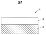
- FIG. 1 is a vertical sectional view of an epitaxial wafer according to the first embodiment.
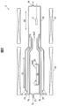
- FIG. 2 is a vertical sectional view of the vapor phase growth apparatus according to the embodiment.
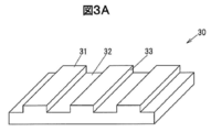
- FIG. 3A is a perspective view showing a part of a main surface of a ⁇ -Ga 2 O 3 single crystal substrate used for evaluation.
- FIG. 3B is a side view showing a part of the main surface of the ⁇ -Ga 2 O 3 single crystal substrate used for the evaluation.
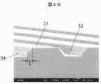
- FIG. 4B is an SEM observation image of a ⁇ -Ga 2 O 3 single crystal substrate in
- FIG. 7 is a graph showing the relationship between the growth rate of the ⁇ -Ga 2 O 3 single crystal by the HVPE method and the plane orientation of the base surface obtained by the evaluation.
- FIG. 8 is a vertical cross-sectional view of a lateral transistor according to the second embodiment.
- FIG. 1 is a vertical sectional view of an epitaxial wafer 10 according to the first embodiment.
- the epitaxial wafer 10 has a semiconductor substrate 11 and an epitaxial layer 12 formed on the main surface of the semiconductor substrate 11 by epitaxial crystal growth by HVPE (Halide Vapor Phase Epitaxy) method.
- HVPE Hydrode Vapor Phase Epitaxy
- the semiconductor substrate 11 is a substrate made of a ⁇ -Ga 2 O 3 based single crystal.
- the ⁇ -Ga 2 O 3 single crystal is a crystal having a ⁇ -Ga 2 O 3 single crystal or a ⁇ -Ga 2 O 3 single crystal to which an element such as Al or In is added as a mother crystal.
- the composition of ⁇ -Ga 2 O 3 single crystal to which Al and In are added is ⁇ - (Ga x Al y In (1-xy) ) 2 O 3 (0 ⁇ x ⁇ 1, 0 ⁇ y ⁇ 1, 0 ⁇ x + y ⁇ 1).
- the semiconductor substrate 11 may contain a conductivity type impurity such as Si.
- the semiconductor substrate 11 is formed by slicing a bulk crystal of a Ga 2 O 3 single crystal grown by a melt growth method such as an FZ (Floating Zone) method or an EFG (Edge Defined Film Fed Growth) method and polishing the surface. Is formed.
- a melt growth method such as an FZ (Floating Zone) method or an EFG (Edge Defined Film Fed Growth) method and polishing the surface. Is formed.
- the main surface of the semiconductor substrate 11 is a surface parallel to the [010] axis of the ⁇ -Ga 2 O 3 single crystal constituting the semiconductor substrate 11. This is because the growth rate of the epitaxial growth by the HVPE method of the ⁇ -Ga 2 O 3 single crystal layer is extremely low when the plane orientation of the main surface of the ⁇ -Ga 2 O 3 single crystal substrate is (010). This is set based on the discovery of the present inventors.
- the inventors of the present invention have the plane orientation of the main surface of the ⁇ -Ga 2 O 3 single crystal substrate that is not suitable for the growth of the ⁇ -Ga 2 O 3 single crystal layer by this HVPE method and is perpendicular to the (010) plane. It has been found that the growth rate of the epitaxial growth by the HVPE method of the ⁇ -Ga 2 O 3 single crystal layer is high when the surface is a plane parallel to the [010] axis.
- the main surface of the semiconductor substrate 11 has a range of 38 ° or more and 90 ° or less in the direction from the (100) plane to the (101) plane with the [010] axis of the ⁇ -Ga 2 O 3 single crystal as the rotation axis. It is the surface rotated by the angle inside.
- the main surface of the semiconductor substrate 11 is rotated by 68 ⁇ 10 ° in the direction from the (100) plane to the (101) plane with the [010] axis of the ⁇ -Ga 2 O 3 single crystal as the rotation axis. It is the surface.
- ⁇ represents an allowable error.
- 68 ⁇ 10 ° represents an arbitrary angle within a range of 58 ° to 78 °.
- the main surface of the semiconductor substrate 11 is 38 ⁇ 1 °, 53.8 ⁇ in the direction from the (100) plane to the (101) plane with the [010] axis of the ⁇ -Ga 2 O 3 single crystal as the rotation axis. It is also preferable that the surface is rotated by 1 °, 68 ⁇ 1 °, 76.3 ⁇ 1 °, 77.3 ⁇ 1 °, 83 ⁇ 1 °, or 90 ⁇ 1 °.
- the epitaxial layer 12 is made of a ⁇ -Ga 2 O 3 single crystal. Further, the epitaxial layer 12 may contain a conductivity type impurity such as Si.
- FIG. 2 is a vertical sectional view of the vapor phase growth apparatus 2 according to the embodiment.
- the vapor phase growth apparatus 2 is a vapor phase growth apparatus for the HVPE method, and includes a first gas introduction port 21, a second gas introduction port 22, a third gas introduction port 23, and an exhaust port 24. 20 and a first heating unit 26 and a second heating unit 27 that are installed around the reaction chamber 20 and heat a predetermined region in the reaction chamber 20.
- the HVPE method has a higher film formation rate than the PLD method or the like.
- the uniformity of the in-plane distribution of film thickness is high, and a large-diameter film can be grown. For this reason, it is suitable for mass production of crystals.
- the reaction chamber 20 is provided with a reaction vessel 25 containing Ga raw material, a raw material reaction region R1 in which a gallium raw material gas is generated, and a crystal growth region in which the semiconductor substrate 11 is disposed and the epitaxial layer 12 is grown. R2 is included.
- the reaction chamber 20 is made of, for example, quartz glass.
- reaction vessel 25 is, for example, quartz glass, and the Ga raw material accommodated in the reaction vessel 25 is metallic gallium.
- the first heating unit 26 and the second heating unit 27 can heat the raw material reaction region R1 and the crystal growth region R2 of the reaction chamber 20, respectively.
- the first heating unit 26 and the second heating unit 27 are, for example, resistance heating type or radiation heating type heating devices.
- the first gas introduction port 21 uses a Cl-containing gas, which is Cl 2 gas or HCl gas, as a raw material reaction region of the reaction chamber 20 using a carrier gas (N 2 gas, Ar gas, or He gas) that is an inert gas. This is a port for introduction into R1.
- a Cl-containing gas which is Cl 2 gas or HCl gas
- a carrier gas N 2 gas, Ar gas, or He gas
- the second gas introduction port 22 is an oxygen-containing gas such as O 2 gas or H 2 O gas, which is an oxygen source gas, and a chloride-based gas (for example, four gases) for adding a dopant such as Si to the epitaxial layer 12.
- This is a port for introducing silicon chloride or the like into the crystal growth region R2 of the reaction chamber 20 using a carrier gas (N 2 gas, Ar gas, or He gas) that is an inert gas.
- the third gas introduction port 23 is a port for introducing a carrier gas (N 2 gas, Ar gas, or He gas) that is an inert gas into the crystal growth region R 2 of the reaction chamber 20.
- a carrier gas N 2 gas, Ar gas, or He gas
- the raw material reaction region R1 of the reaction chamber 20 is heated using the first heating means 26, and the atmospheric temperature of the raw material reaction region R1 is maintained at a predetermined temperature.
- a Cl-containing gas is introduced from the first gas introduction port 21 using a carrier gas, and the metal gallium and the Cl-containing gas in the reaction vessel 25 are reacted in the raw material reaction region R1 at the above atmospheric temperature. Generates gallium chloride gas.
- the atmospheric temperature in the raw material reaction region R1 is such that the partial pressure of the GaCl gas is the highest among the gallium chloride-based gases generated by the reaction between the metal gallium in the reaction vessel 25 and the Cl-containing gas. Temperature is preferred.
- the gallium chloride-based gas includes GaCl gas, GaCl 2 gas, GaCl 3 gas, (GaCl 3 ) 2 gas, and the like.
- GaCl gas is a gas that can maintain the growth driving force of Ga 2 O 3 crystals up to the highest temperature among the gases contained in the gallium chloride-based gas. High purity, in order to obtain a high quality Ga 2 O 3 crystal, for growth at high growth temperatures are valid, and generates the partial pressure is higher gallium chloride gas of high GaCl gas growth driving force at a high temperature Is preferred for the growth of the epitaxial layer 12.
- Cl 2 gas not containing hydrogen is used as the Cl-containing gas. It is preferable to use it.
- the metal gallium in the reaction vessel 25 is maintained in a state where the atmosphere temperature of the raw material reaction region R1 is maintained at 300 ° C. or higher by the first heating means 26. It is preferable to react a Cl-containing gas.
- the partial pressure ratio of GaCl gas is overwhelmingly high (the equilibrium partial pressure of GaCl gas is 4 orders of magnitude higher than GaCl 2 gas and 8 orders of magnitude higher than GaCl 3 gas). Gases other than GaCl gas hardly contribute to the growth of Ga 2 O 3 crystals.
- the metal in the reaction vessel 25 is maintained in a state where the atmosphere temperature of the raw material reaction region R1 is kept at 1000 ° C. or lower. It is preferable to react gallium with a Cl-containing gas.
- the gallium chloride gas generated in the raw material reaction region R1 and the oxygen-containing gas introduced from the second gas introduction port 22 are mixed, and the semiconductor substrate 11 is mixed with the mixed gas.
- the epitaxial layer 12 is epitaxially grown on the semiconductor substrate 11 by exposure.
- the pressure in the crystal growth region R2 in the furnace containing the reaction chamber 20 is maintained at, for example, 1 atm.
- a source gas of the additive element for example, a chloride-based gas such as silicon tetrachloride (SiCl 4 )
- SiCl 4 silicon tetrachloride
- O 2 gas not containing hydrogen is used as the oxygen-containing gas. It is preferable to use it.
- the ratio of the O 2 gas supply partial pressure to the GaCl gas supply partial pressure in the crystal growth region R2 is 0.
- the epitaxial layer 12 is preferably grown in a state of 5 or more.
- the growth temperature is preferably set to 900 ° C. or higher.
- the epitaxial layer 12 contains, for example, 5 ⁇ 10 16 (atoms / cm 3 ) or less of Cl. This is because the epitaxial layer 12 is formed by the HVPE method using a Cl-containing gas. Normally, when a Ga 2 O 3 single crystal film is formed by a method other than the HVPE method, since a Cl-containing gas is not used, Cl is not contained in the Ga 2 O 3 single crystal film. ⁇ 10 16 (atoms / cm 3 ) does not contain more Cl.
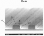
- 3A and 3B are a perspective view and a side view showing a part of the main surface of the ⁇ -Ga 2 O 3 single crystal substrate 30 used for the evaluation.
- the upper surface of the convex portion of the main surface of the ⁇ -Ga 2 O 3 single crystal substrate 30 is defined as a surface 31, the bottom surface of the concave portion is defined as a surface 32, and the side surfaces of the convex portion are defined as surfaces 33 and 34.
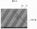
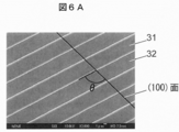
- the plane orientation of the planes 31 and 32 is (010).
- the surfaces 33 and 34 are surfaces perpendicular to the surfaces 31 and 32 and are rotated by an angle ⁇ in the direction from the (100) plane to the (101) plane with the [010] axis as the rotation axis. Note that the surface orientation of the surface 34 is further rotated 180 ° from ⁇ , which is equivalent to the surface orientation of the surface 33.
- 4A is an image observed from a direction perpendicular to the principal surface
- FIG. 4B is an image observed obliquely from above.
- 5A is an image observed from a direction perpendicular to the main surface
- FIG. 5B is an image observed from obliquely above.
- 6A is an image observed from a direction perpendicular to the main surface
- FIG. 6B is an image observed from obliquely above.
- the thickness t shown in FIG. 4B, FIG. 5B, and FIG. 6B represents the thickness of the ⁇ -Ga 2 O 3 single crystal grown in the direction perpendicular to the surfaces 33 and.
- FIG. 7 is a graph showing the relationship between the growth rate of the ⁇ -Ga 2 O 3 single crystal by the HVPE method and the plane orientation of the base surface obtained by the evaluation. 7 represents the angle ⁇ of the surface 33, and the vertical axis represents the growth rate of ⁇ -Ga 2 O 3 single crystal in the direction perpendicular to the surfaces 33 and 34 (increase amount per unit time of the thickness t). To express.
- the plot mark ⁇ in FIG. 7 is a measured value by the evaluation method using the ⁇ -Ga 2 O 3 single crystal substrate 30 described above.
- Plot marks ⁇ is, ⁇ -Ga 2 O 3 without using the single crystal substrate 30, the corresponding flat main surface ⁇ -Ga 2 O 3 on a single crystal substrate ⁇ -Ga 2 O 3 single crystal having a plane orientation Is a measured value obtained by observing the growth in the direction perpendicular to the main surface.
- Table 1 below shows the numerical values at each measurement point shown in FIG.
- the growth rate of the ⁇ -Ga 2 O 3 single crystal on the plane parallel to the [010] axis is on the (010) plane in the entire range of 0 ⁇ ⁇ ⁇ 180 °. It is much higher than the growth rate.
- the growth rate of the ⁇ -Ga 2 O 3 single crystal is particularly high in the range of 38 ° ⁇ ⁇ ⁇ 90 °.
- the growth rate of the ⁇ -Ga 2 O 3 single crystal tends to increase as the angle ⁇ approaches 68 °, and the range of 68 ⁇ 10 ° is particularly high. It is estimated that a high growth rate can be obtained.
- the growth rate of the ⁇ -Ga 2 O 3 single crystal is high when the angle is 68 ° ⁇ 1 °, 76.3 ⁇ 1 °, 77.3 ⁇ 1 °, 83 ⁇ 1 °, or 90 ⁇ 1 °.
- the above evaluation was performed by growing a ⁇ -Ga 2 O 3 single crystal on a ⁇ -Ga 2 O 3 single crystal substrate.
- a ⁇ -Ga 2 O 3 single crystal was used as a substrate material and a growth crystal. Similar results can be obtained when evaluation is performed using another ⁇ -Ga 2 O 3 single crystal instead or when evaluation is performed using a ⁇ -Ga 2 O 3 single crystal containing a dopant. .
- the main surface of the semiconductor substrate 11 of the epitaxial wafer 10 is preferably a plane parallel to the [010] axis in order to increase the growth rate of the epitaxial growth of the epitaxial layer 12 by the HVPE method.
- the main surface of the semiconductor substrate 11 is in the range of 38 ° or more and 90 ° or less in the direction from the (100) plane to the (101) plane with the [010] axis of the ⁇ -Ga 2 O 3 single crystal as the rotation axis. It can be said that the surface rotated at an angle of is more preferable.
- the main surface of the semiconductor substrate 11 is a surface rotated by 68 ⁇ 10 ° in the direction from the (100) plane to the (101) plane with the [010] axis of the ⁇ -Ga 2 O 3 single crystal as the rotation axis. It can be said that it is more preferable.
- the main surface of the semiconductor substrate 11 is 38 ⁇ 1 °, 53.8 ⁇ in the direction from the (100) plane to the (101) plane with the [010] axis of the ⁇ -Ga 2 O 3 single crystal as the rotation axis. It can also be said that the surface is preferably rotated by 1 °, 68 ⁇ 1 °, 76.3 ⁇ 1 °, 77.3 ⁇ 1 °, 83 ⁇ 1 °, or 90 ⁇ 1 °.
- the second embodiment is a form of a semiconductor element including the epitaxial wafer 10 according to the first embodiment.
- a lateral transistor having a MESFET (Metal Semiconductor Field Effect Transistor) structure will be described.
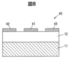
- FIG. 8 is a vertical sectional view of a lateral transistor 40 according to the second embodiment.
- the lateral transistor 40 includes an epitaxial layer 12 formed on the semiconductor substrate 11, a gate electrode 41 on the epitaxial layer 12, a source electrode 42, and a drain electrode 43.
- the gate electrode 41 is disposed between the source electrode 42 and the drain electrode 43.
- the source electrode 42 and the drain electrode 43 are in contact with the upper surface of the epitaxial layer 12 (the surface opposite to the surface in contact with the semiconductor substrate 11) to form an ohmic junction. Further, the gate electrode 41 contacts the upper surface of the epitaxial layer 12 to form a Schottky junction, and a depletion layer is formed under the gate electrode 41 in the epitaxial layer 12. Depending on the thickness of the depletion region, the lateral transistor 40 functions as a normally-off transistor or a normally-on transistor.
- the semiconductor substrate 11 is made of a Ga 2 O 3 based crystal containing a p-type dopant such as Mg, Be, Zn, or Fe, and has a high electric resistance.
- the epitaxial layer 12 includes an n-type dopant such as Si or Sn.
- concentration of the n-type dopant in the vicinity of the contact portion with the source electrode 42 and the drain electrode 43 is higher than the concentration of the n-type dopant in other portions.
- the thickness of the epitaxial layer 12 is, for example, 0.1 to 1 ⁇ m.
- the gate electrode 41, the source electrode 42, and the drain electrode 43 are, for example, metals such as Au, Al, Ti, Sn, Ge, In, Ni, Co, Pt, W, Mo, Cr, Cu, and Pb, and these metals. It consists of an alloy containing two or more of these, a conductive compound such as ITO, or a conductive polymer.
- a conductive compound such as ITO, or a conductive polymer.
- a polythiophene derivative PEDOT: poly (3,4) -ethylenedioxythiophene
- PPS polystyrene sulfonic acid
- the gate electrode 41 may have a two-layer structure made of two different metals, for example, Al / Ti, Au / Ni, Au / Co.
- the drain current can be controlled by changing the thickness of the depletion layer under the gate electrode 41 in the epitaxial layer 12 by controlling the bias voltage applied to the gate electrode 41.
- the above-described lateral transistor 40 is an example of a semiconductor element including the epitaxial wafer 10 according to the first embodiment, and in addition, various semiconductor elements can be manufactured using the epitaxial wafer 10.
- a MISFET Metal Insulator Semiconductor Field Field Effect Transistor
- HEMT High Electron Mobility Transistor
- Etc. can be manufactured.
- the type and concentration of the dopant contained in the semiconductor substrate 11 and the epitaxial layer 12 are appropriately set.
- an epitaxial wafer can be efficiently produced by epitaxially growing an epitaxial layer on the semiconductor substrate. Further, since the diffusion of impurities from the semiconductor substrate can be suppressed by growing the epitaxial layer at a high growth rate, this epitaxial wafer has a high-quality epitaxial layer.
- a semiconductor substrate made of ⁇ -Ga 2 O 3 single crystal capable of growing an epitaxial layer made of ⁇ -Ga 2 O 3 single crystal at a high growth rate by the HVPE method, an epitaxial wafer having the semiconductor substrate and the epitaxial layer, and A method for manufacturing the epitaxial wafer is provided.
Landscapes
- Engineering & Computer Science (AREA)
- Chemical & Material Sciences (AREA)
- Manufacturing & Machinery (AREA)
- Physics & Mathematics (AREA)
- Computer Hardware Design (AREA)
- Microelectronics & Electronic Packaging (AREA)
- Power Engineering (AREA)
- Condensed Matter Physics & Semiconductors (AREA)
- General Physics & Mathematics (AREA)
- Materials Engineering (AREA)
- Crystallography & Structural Chemistry (AREA)
- Organic Chemistry (AREA)
- Metallurgy (AREA)
- Chemical Kinetics & Catalysis (AREA)
- General Chemical & Material Sciences (AREA)
- Inorganic Chemistry (AREA)
- Mechanical Engineering (AREA)
- Crystals, And After-Treatments Of Crystals (AREA)
- Chemical Vapour Deposition (AREA)
Priority Applications (3)
| Application Number | Priority Date | Filing Date | Title |
|---|---|---|---|
| US15/309,956 US10676841B2 (en) | 2014-05-09 | 2015-05-11 | Semiconductor substrate, epitaxial wafer, and method for manufacturing epitaxial wafer |
| EP15789328.0A EP3141635B1 (en) | 2014-05-09 | 2015-05-11 | Semiconductor substrate, epitaxial wafer, and method for manufacturing epitaxial wafer |
| CN201580024046.XA CN106471163B (zh) | 2014-05-09 | 2015-05-11 | 半导体衬底、外延片及其制造方法 |
Applications Claiming Priority (2)
| Application Number | Priority Date | Filing Date | Title |
|---|---|---|---|
| JP2014097751A JP6253150B2 (ja) | 2014-05-09 | 2014-05-09 | エピタキシャルウエハ及びその製造方法 |
| JP2014-097751 | 2014-05-09 |
Publications (1)
| Publication Number | Publication Date |
|---|---|
| WO2015170774A1 true WO2015170774A1 (ja) | 2015-11-12 |
Family
ID=54392621
Family Applications (1)
| Application Number | Title | Priority Date | Filing Date |
|---|---|---|---|
| PCT/JP2015/063523 Ceased WO2015170774A1 (ja) | 2014-05-09 | 2015-05-11 | 半導体基板、並びにエピタキシャルウエハ及びその製造方法 |
Country Status (6)
| Country | Link |
|---|---|
| US (1) | US10676841B2 (OSRAM) |
| EP (1) | EP3141635B1 (OSRAM) |
| JP (1) | JP6253150B2 (OSRAM) |
| CN (1) | CN106471163B (OSRAM) |
| TW (1) | TWI721945B (OSRAM) |
| WO (1) | WO2015170774A1 (OSRAM) |
Cited By (1)
| Publication number | Priority date | Publication date | Assignee | Title |
|---|---|---|---|---|
| CN108368641A (zh) * | 2015-12-16 | 2018-08-03 | 株式会社田村制作所 | 半导体基板、以及外延晶片及其制造方法 |
Families Citing this family (5)
| Publication number | Priority date | Publication date | Assignee | Title |
|---|---|---|---|---|
| JP5984069B2 (ja) * | 2013-09-30 | 2016-09-06 | 株式会社タムラ製作所 | β−Ga2O3系単結晶膜の成長方法、及び結晶積層構造体 |
| CN113614292B (zh) * | 2019-03-28 | 2024-08-23 | 日本碍子株式会社 | 半导体膜 |
| CN113394079A (zh) * | 2021-06-18 | 2021-09-14 | 中国电子科技集团公司第四十六研究所 | 一种采用卤化物气相外延法生长氧化镓外延层的方法 |
| DE112021008176T5 (de) * | 2021-09-03 | 2024-06-27 | Mitsubishi Electric Corporation | Kristall-laminierungsstruktur, halbleitereinrichtung und verfahren zum herstellen einer kristall-laminierungsstruktur |
| JPWO2024048710A1 (OSRAM) * | 2022-08-31 | 2024-03-07 |
Citations (4)
| Publication number | Priority date | Publication date | Assignee | Title |
|---|---|---|---|---|
| WO2013035464A1 (ja) * | 2011-09-08 | 2013-03-14 | 株式会社タムラ製作所 | 結晶積層構造体及びその製造方法 |
| JP2013227202A (ja) * | 2012-03-30 | 2013-11-07 | Mitsubishi Chemicals Corp | 周期表第13族金属窒化物半導体結晶の製造方法、および、当該製造方法によって得られた周期表第13族金属窒化物半導体結晶を用いた半導体発光デバイス |
| JP2013229554A (ja) * | 2012-03-30 | 2013-11-07 | Mitsubishi Chemicals Corp | 周期表第13族金属窒化物半導体結晶の製造方法、それに用いるノズルおよび製造装置 |
| JP2015091740A (ja) * | 2013-09-30 | 2015-05-14 | 株式会社タムラ製作所 | β−Ga2O3系単結晶膜の成長方法、及び結晶積層構造体 |
Family Cites Families (10)
| Publication number | Priority date | Publication date | Assignee | Title |
|---|---|---|---|---|
| US7008839B2 (en) * | 2002-03-08 | 2006-03-07 | Matsushita Electric Industrial Co., Ltd. | Method for manufacturing semiconductor thin film |
| JP4680762B2 (ja) | 2005-12-14 | 2011-05-11 | 株式会社光波 | 発光素子及びその製造方法 |
| US20070134833A1 (en) | 2005-12-14 | 2007-06-14 | Toyoda Gosei Co., Ltd. | Semiconductor element and method of making same |
| GB2436398B (en) * | 2006-03-23 | 2011-08-24 | Univ Bath | Growth method using nanostructure compliant layers and HVPE for producing high quality compound semiconductor materials |
| KR100969127B1 (ko) * | 2010-02-18 | 2010-07-09 | 엘지이노텍 주식회사 | 발광 소자, 발광 소자 제조방법 및 발광 소자 패키지 |
| CN101967680B (zh) * | 2010-11-04 | 2012-02-01 | 山东大学 | 一种在氧化镁衬底上制备单斜晶型氧化镓单晶薄膜的方法 |
| CN110071170B (zh) | 2011-09-08 | 2022-10-11 | 株式会社田村制作所 | 晶体层叠结构体 |
| CN110047922A (zh) | 2011-09-08 | 2019-07-23 | 株式会社田村制作所 | Ga2O3系MISFET和Ga2O3系MESFET |
| CN103765593B (zh) * | 2011-09-08 | 2017-06-09 | 株式会社田村制作所 | Ga2O3系半导体元件 |
| CN103489967B (zh) * | 2013-09-05 | 2016-07-13 | 大连理工大学 | 一种氧化镓外延膜的制备方法及氧化镓外延膜 |
-
2014
- 2014-05-09 JP JP2014097751A patent/JP6253150B2/ja active Active
-
2015
- 2015-05-11 TW TW104114927A patent/TWI721945B/zh active
- 2015-05-11 EP EP15789328.0A patent/EP3141635B1/en active Active
- 2015-05-11 WO PCT/JP2015/063523 patent/WO2015170774A1/ja not_active Ceased
- 2015-05-11 CN CN201580024046.XA patent/CN106471163B/zh active Active
- 2015-05-11 US US15/309,956 patent/US10676841B2/en active Active
Patent Citations (4)
| Publication number | Priority date | Publication date | Assignee | Title |
|---|---|---|---|---|
| WO2013035464A1 (ja) * | 2011-09-08 | 2013-03-14 | 株式会社タムラ製作所 | 結晶積層構造体及びその製造方法 |
| JP2013227202A (ja) * | 2012-03-30 | 2013-11-07 | Mitsubishi Chemicals Corp | 周期表第13族金属窒化物半導体結晶の製造方法、および、当該製造方法によって得られた周期表第13族金属窒化物半導体結晶を用いた半導体発光デバイス |
| JP2013229554A (ja) * | 2012-03-30 | 2013-11-07 | Mitsubishi Chemicals Corp | 周期表第13族金属窒化物半導体結晶の製造方法、それに用いるノズルおよび製造装置 |
| JP2015091740A (ja) * | 2013-09-30 | 2015-05-14 | 株式会社タムラ製作所 | β−Ga2O3系単結晶膜の成長方法、及び結晶積層構造体 |
Non-Patent Citations (1)
| Title |
|---|
| See also references of EP3141635A4 * |
Cited By (4)
| Publication number | Priority date | Publication date | Assignee | Title |
|---|---|---|---|---|
| CN108368641A (zh) * | 2015-12-16 | 2018-08-03 | 株式会社田村制作所 | 半导体基板、以及外延晶片及其制造方法 |
| EP3396030A4 (en) * | 2015-12-16 | 2019-07-24 | Tamura Corporation | SEMICONDUCTOR SUBSTRATE AND EPITACTIC WAFER AND METHOD FOR THE PRODUCTION THEREOF |
| US10985016B2 (en) | 2015-12-16 | 2021-04-20 | Tamura Corporation | Semiconductor substrate, and epitaxial wafer and method for producing same |
| CN108368641B (zh) * | 2015-12-16 | 2021-04-27 | 株式会社田村制作所 | 半导体基板、以及外延晶片及其制造方法 |
Also Published As
| Publication number | Publication date |
|---|---|
| JP2015214448A (ja) | 2015-12-03 |
| TW201606114A (zh) | 2016-02-16 |
| TWI721945B (zh) | 2021-03-21 |
| CN106471163A (zh) | 2017-03-01 |
| EP3141635B1 (en) | 2023-05-03 |
| CN106471163B (zh) | 2020-03-24 |
| EP3141635A4 (en) | 2018-01-10 |
| EP3141635A1 (en) | 2017-03-15 |
| US10676841B2 (en) | 2020-06-09 |
| US20170145590A1 (en) | 2017-05-25 |
| JP6253150B2 (ja) | 2017-12-27 |
Similar Documents
| Publication | Publication Date | Title |
|---|---|---|
| US11982016B2 (en) | Method for growing beta-Ga2O3-based single crystal film, and crystalline layered structure | |
| JP6744523B2 (ja) | 半導体基板、並びにエピタキシャルウエハ及びその製造方法 | |
| JP5018423B2 (ja) | Iii族窒化物半導体結晶基板および半導体デバイス | |
| JP6253150B2 (ja) | エピタキシャルウエハ及びその製造方法 | |
| CN107534062B (zh) | 高耐压肖特基势垒二极管 | |
| WO2016152335A1 (ja) | 結晶積層構造体 | |
| US9418840B2 (en) | Silicon carbide semiconductor device manufacturing method and silicon carbide semiconductor device | |
| KR102785434B1 (ko) | GaN 결정 및 기판 | |
| JP6875708B2 (ja) | 結晶積層構造体、及びそれを製造する方法 | |
| US20120104557A1 (en) | Method for manufacturing a group III nitride crystal, method for manufacturing a group III nitride template, group III nitride crystal and group III nitride template | |
| JP5135708B2 (ja) | Iii族窒化物系電子デバイスおよびエピタキシャル基板 | |
| JP5641029B2 (ja) | Iii族窒化物系電子デバイス | |
| WO2023058493A1 (ja) | エピタキシャル層のキャリア濃度を均一化する方法及びそれらの方法により作製された構造 |
Legal Events
| Date | Code | Title | Description |
|---|---|---|---|
| 121 | Ep: the epo has been informed by wipo that ep was designated in this application |
Ref document number: 15789328 Country of ref document: EP Kind code of ref document: A1 |
|
| NENP | Non-entry into the national phase |
Ref country code: DE |
|
| WWE | Wipo information: entry into national phase |
Ref document number: 15309956 Country of ref document: US |
|
| REEP | Request for entry into the european phase |
Ref document number: 2015789328 Country of ref document: EP |
|
| WWE | Wipo information: entry into national phase |
Ref document number: 2015789328 Country of ref document: EP |