WO2015170699A1 - 酸化物超電導線材及び酸化物超電導線材の製造方法 - Google Patents
酸化物超電導線材及び酸化物超電導線材の製造方法 Download PDFInfo
- Publication number
- WO2015170699A1 WO2015170699A1 PCT/JP2015/063184 JP2015063184W WO2015170699A1 WO 2015170699 A1 WO2015170699 A1 WO 2015170699A1 JP 2015063184 W JP2015063184 W JP 2015063184W WO 2015170699 A1 WO2015170699 A1 WO 2015170699A1
- Authority
- WO
- WIPO (PCT)
- Prior art keywords
- oxide superconducting
- layer
- orientation
- region
- superconducting wire
- Prior art date
Links
- 239000000463 material Substances 0.000 title claims abstract description 116
- 238000004519 manufacturing process Methods 0.000 title claims description 29
- 239000013078 crystal Substances 0.000 claims abstract description 30
- 230000002401 inhibitory effect Effects 0.000 claims description 55
- 239000000758 substrate Substances 0.000 claims description 49
- 238000000034 method Methods 0.000 claims description 40
- 238000012545 processing Methods 0.000 claims description 40
- 230000005764 inhibitory process Effects 0.000 claims description 20
- 239000003795 chemical substances by application Substances 0.000 claims description 14
- 238000010030 laminating Methods 0.000 claims description 7
- 230000001678 irradiating effect Effects 0.000 claims description 4
- 238000003825 pressing Methods 0.000 claims description 4
- 239000010410 layer Substances 0.000 description 573
- 229910052751 metal Inorganic materials 0.000 description 45
- 239000002184 metal Substances 0.000 description 45
- 230000005415 magnetization Effects 0.000 description 33
- 238000012360 testing method Methods 0.000 description 26
- 230000002829 reductive effect Effects 0.000 description 21
- 230000000087 stabilizing effect Effects 0.000 description 19
- 238000005530 etching Methods 0.000 description 16
- 239000010949 copper Substances 0.000 description 15
- 239000010408 film Substances 0.000 description 15
- 230000006641 stabilisation Effects 0.000 description 13
- 238000011105 stabilization Methods 0.000 description 13
- 238000005259 measurement Methods 0.000 description 12
- 230000015572 biosynthetic process Effects 0.000 description 8
- 239000011248 coating agent Substances 0.000 description 7
- 239000011247 coating layer Substances 0.000 description 7
- 238000000576 coating method Methods 0.000 description 7
- 238000010586 diagram Methods 0.000 description 7
- 238000009792 diffusion process Methods 0.000 description 7
- 238000007735 ion beam assisted deposition Methods 0.000 description 7
- 238000012993 chemical processing Methods 0.000 description 6
- 238000007747 plating Methods 0.000 description 6
- 230000002265 prevention Effects 0.000 description 6
- 229920005989 resin Polymers 0.000 description 6
- 239000011347 resin Substances 0.000 description 6
- 229910018072 Al 2 O 3 Inorganic materials 0.000 description 5
- RYGMFSIKBFXOCR-UHFFFAOYSA-N Copper Chemical compound [Cu] RYGMFSIKBFXOCR-UHFFFAOYSA-N 0.000 description 5
- 229910045601 alloy Inorganic materials 0.000 description 5
- 239000000956 alloy Substances 0.000 description 5
- 229910052802 copper Inorganic materials 0.000 description 5
- CSCPPACGZOOCGX-UHFFFAOYSA-N Acetone Chemical compound CC(C)=O CSCPPACGZOOCGX-UHFFFAOYSA-N 0.000 description 4
- 230000007423 decrease Effects 0.000 description 4
- 230000000873 masking effect Effects 0.000 description 4
- 230000008569 process Effects 0.000 description 4
- 239000011241 protective layer Substances 0.000 description 4
- 238000001878 scanning electron micrograph Methods 0.000 description 4
- 238000004544 sputter deposition Methods 0.000 description 4
- 239000002887 superconductor Substances 0.000 description 4
- 238000004804 winding Methods 0.000 description 4
- 229910001316 Ag alloy Inorganic materials 0.000 description 3
- PXHVJJICTQNCMI-UHFFFAOYSA-N Nickel Chemical compound [Ni] PXHVJJICTQNCMI-UHFFFAOYSA-N 0.000 description 3
- GRYLNZFGIOXLOG-UHFFFAOYSA-N Nitric acid Chemical compound O[N+]([O-])=O GRYLNZFGIOXLOG-UHFFFAOYSA-N 0.000 description 3
- 239000004020 conductor Substances 0.000 description 3
- 238000005520 cutting process Methods 0.000 description 3
- 230000000694 effects Effects 0.000 description 3
- 238000010894 electron beam technology Methods 0.000 description 3
- 238000003475 lamination Methods 0.000 description 3
- 239000007769 metal material Substances 0.000 description 3
- 229910017604 nitric acid Inorganic materials 0.000 description 3
- 238000004549 pulsed laser deposition Methods 0.000 description 3
- 238000012546 transfer Methods 0.000 description 3
- -1 2 O 3 Chemical class 0.000 description 2
- IJGRMHOSHXDMSA-UHFFFAOYSA-N Atomic nitrogen Chemical compound N#N IJGRMHOSHXDMSA-UHFFFAOYSA-N 0.000 description 2
- 241000954177 Bangana ariza Species 0.000 description 2
- 229910017493 Nd 2 O 3 Inorganic materials 0.000 description 2
- XUIMIQQOPSSXEZ-UHFFFAOYSA-N Silicon Chemical compound [Si] XUIMIQQOPSSXEZ-UHFFFAOYSA-N 0.000 description 2
- BQCADISMDOOEFD-UHFFFAOYSA-N Silver Chemical compound [Ag] BQCADISMDOOEFD-UHFFFAOYSA-N 0.000 description 2
- 239000000853 adhesive Substances 0.000 description 2
- 238000004364 calculation method Methods 0.000 description 2
- 239000011651 chromium Substances 0.000 description 2
- 239000000470 constituent Substances 0.000 description 2
- 230000006866 deterioration Effects 0.000 description 2
- 238000002050 diffraction method Methods 0.000 description 2
- 239000003822 epoxy resin Substances 0.000 description 2
- 229910000856 hastalloy Inorganic materials 0.000 description 2
- 238000010438 heat treatment Methods 0.000 description 2
- 229910052757 nitrogen Inorganic materials 0.000 description 2
- 229920000647 polyepoxide Polymers 0.000 description 2
- 229920001721 polyimide Polymers 0.000 description 2
- 238000002360 preparation method Methods 0.000 description 2
- 229910052761 rare earth metal Inorganic materials 0.000 description 2
- 239000010703 silicon Substances 0.000 description 2
- 229910052710 silicon Inorganic materials 0.000 description 2
- 229910052709 silver Inorganic materials 0.000 description 2
- 239000004332 silver Substances 0.000 description 2
- 239000007921 spray Substances 0.000 description 2
- 230000003746 surface roughness Effects 0.000 description 2
- 239000010409 thin film Substances 0.000 description 2
- 239000004925 Acrylic resin Substances 0.000 description 1
- 229920000178 Acrylic resin Polymers 0.000 description 1
- 229910000838 Al alloy Inorganic materials 0.000 description 1
- 229910052684 Cerium Inorganic materials 0.000 description 1
- VYZAMTAEIAYCRO-UHFFFAOYSA-N Chromium Chemical compound [Cr] VYZAMTAEIAYCRO-UHFFFAOYSA-N 0.000 description 1
- 229910017518 Cu Zn Inorganic materials 0.000 description 1
- 229910000881 Cu alloy Inorganic materials 0.000 description 1
- 229910017752 Cu-Zn Inorganic materials 0.000 description 1
- 229910002482 Cu–Ni Inorganic materials 0.000 description 1
- 229910017943 Cu—Zn Inorganic materials 0.000 description 1
- 229910052692 Dysprosium Inorganic materials 0.000 description 1
- 229910052691 Erbium Inorganic materials 0.000 description 1
- 229910052693 Europium Inorganic materials 0.000 description 1
- 229910052688 Gadolinium Inorganic materials 0.000 description 1
- 229910052689 Holmium Inorganic materials 0.000 description 1
- XEEYBQQBJWHFJM-UHFFFAOYSA-N Iron Chemical compound [Fe] XEEYBQQBJWHFJM-UHFFFAOYSA-N 0.000 description 1
- 229910021193 La 2 O 3 Inorganic materials 0.000 description 1
- 229910052765 Lutetium Inorganic materials 0.000 description 1
- 229920000877 Melamine resin Polymers 0.000 description 1
- 239000004640 Melamine resin Substances 0.000 description 1
- ZOKXTWBITQBERF-UHFFFAOYSA-N Molybdenum Chemical compound [Mo] ZOKXTWBITQBERF-UHFFFAOYSA-N 0.000 description 1
- 229910052779 Neodymium Inorganic materials 0.000 description 1
- 239000004642 Polyimide Substances 0.000 description 1
- 229910052777 Praseodymium Inorganic materials 0.000 description 1
- 229910052772 Samarium Inorganic materials 0.000 description 1
- 229910002367 SrTiO Inorganic materials 0.000 description 1
- 229910052771 Terbium Inorganic materials 0.000 description 1
- 229910052775 Thulium Inorganic materials 0.000 description 1
- 229910052769 Ytterbium Inorganic materials 0.000 description 1
- 238000007792 addition Methods 0.000 description 1
- 230000001070 adhesive effect Effects 0.000 description 1
- 229920000180 alkyd Polymers 0.000 description 1
- 229910052782 aluminium Inorganic materials 0.000 description 1
- XAGFODPZIPBFFR-UHFFFAOYSA-N aluminium Chemical compound [Al] XAGFODPZIPBFFR-UHFFFAOYSA-N 0.000 description 1
- PNEYBMLMFCGWSK-UHFFFAOYSA-N aluminium oxide Inorganic materials [O-2].[O-2].[O-2].[Al+3].[Al+3] PNEYBMLMFCGWSK-UHFFFAOYSA-N 0.000 description 1
- 238000000137 annealing Methods 0.000 description 1
- QVGXLLKOCUKJST-UHFFFAOYSA-N atomic oxygen Chemical compound [O] QVGXLLKOCUKJST-UHFFFAOYSA-N 0.000 description 1
- 230000008859 change Effects 0.000 description 1
- 238000006243 chemical reaction Methods 0.000 description 1
- 229910052804 chromium Inorganic materials 0.000 description 1
- 229910017052 cobalt Inorganic materials 0.000 description 1
- 239000010941 cobalt Substances 0.000 description 1
- GUTLYIVDDKVIGB-UHFFFAOYSA-N cobalt atom Chemical compound [Co] GUTLYIVDDKVIGB-UHFFFAOYSA-N 0.000 description 1
- 238000001816 cooling Methods 0.000 description 1
- TVZPLCNGKSPOJA-UHFFFAOYSA-N copper zinc Chemical compound [Cu].[Zn] TVZPLCNGKSPOJA-UHFFFAOYSA-N 0.000 description 1
- 238000001035 drying Methods 0.000 description 1
- 238000001887 electron backscatter diffraction Methods 0.000 description 1
- 238000011156 evaluation Methods 0.000 description 1
- 230000004907 flux Effects 0.000 description 1
- 239000012535 impurity Substances 0.000 description 1
- 238000001659 ion-beam spectroscopy Methods 0.000 description 1
- 229910052746 lanthanum Inorganic materials 0.000 description 1
- 230000000670 limiting effect Effects 0.000 description 1
- 239000007788 liquid Substances 0.000 description 1
- 238000003754 machining Methods 0.000 description 1
- 229910044991 metal oxide Inorganic materials 0.000 description 1
- 150000004706 metal oxides Chemical class 0.000 description 1
- 150000002739 metals Chemical class 0.000 description 1
- 238000002156 mixing Methods 0.000 description 1
- 230000004048 modification Effects 0.000 description 1
- 238000012986 modification Methods 0.000 description 1
- 229910052750 molybdenum Inorganic materials 0.000 description 1
- 239000011733 molybdenum Substances 0.000 description 1
- 229910052759 nickel Inorganic materials 0.000 description 1
- 239000001301 oxygen Substances 0.000 description 1
- 229910052760 oxygen Inorganic materials 0.000 description 1
- 239000002245 particle Substances 0.000 description 1
- 238000005192 partition Methods 0.000 description 1
- 239000005011 phenolic resin Substances 0.000 description 1
- 229920006122 polyamide resin Polymers 0.000 description 1
- 229920001225 polyester resin Polymers 0.000 description 1
- 239000004645 polyester resin Substances 0.000 description 1
- 239000009719 polyimide resin Substances 0.000 description 1
- 239000002994 raw material Substances 0.000 description 1
- 230000009257 reactivity Effects 0.000 description 1
- 230000011218 segmentation Effects 0.000 description 1
- 229910000679 solder Inorganic materials 0.000 description 1
- 239000010935 stainless steel Substances 0.000 description 1
- 229910001220 stainless steel Inorganic materials 0.000 description 1
- 230000003068 static effect Effects 0.000 description 1
- 239000000126 substance Substances 0.000 description 1
- 238000006467 substitution reaction Methods 0.000 description 1
- 230000007704 transition Effects 0.000 description 1
- 229910052721 tungsten Inorganic materials 0.000 description 1
- 125000000391 vinyl group Chemical group [H]C([*])=C([H])[H] 0.000 description 1
- 229920002554 vinyl polymer Polymers 0.000 description 1
- 229910052727 yttrium Inorganic materials 0.000 description 1
Images


Classifications
-
- H—ELECTRICITY
- H10—SEMICONDUCTOR DEVICES; ELECTRIC SOLID-STATE DEVICES NOT OTHERWISE PROVIDED FOR
- H10N—ELECTRIC SOLID-STATE DEVICES NOT OTHERWISE PROVIDED FOR
- H10N60/00—Superconducting devices
- H10N60/80—Constructional details
- H10N60/85—Superconducting active materials
- H10N60/855—Ceramic superconductors
- H10N60/857—Ceramic superconductors comprising copper oxide
- H10N60/858—Ceramic superconductors comprising copper oxide having multilayered structures, e.g. superlattices
-
- H—ELECTRICITY
- H01—ELECTRIC ELEMENTS
- H01B—CABLES; CONDUCTORS; INSULATORS; SELECTION OF MATERIALS FOR THEIR CONDUCTIVE, INSULATING OR DIELECTRIC PROPERTIES
- H01B12/00—Superconductive or hyperconductive conductors, cables, or transmission lines
- H01B12/02—Superconductive or hyperconductive conductors, cables, or transmission lines characterised by their form
-
- H—ELECTRICITY
- H10—SEMICONDUCTOR DEVICES; ELECTRIC SOLID-STATE DEVICES NOT OTHERWISE PROVIDED FOR
- H10N—ELECTRIC SOLID-STATE DEVICES NOT OTHERWISE PROVIDED FOR
- H10N60/00—Superconducting devices
- H10N60/01—Manufacture or treatment
- H10N60/0268—Manufacture or treatment of devices comprising copper oxide
- H10N60/0296—Processes for depositing or forming copper oxide superconductor layers
- H10N60/0576—Processes for depositing or forming copper oxide superconductor layers characterised by the substrate
- H10N60/0632—Intermediate layers, e.g. for growth control
-
- H—ELECTRICITY
- H10—SEMICONDUCTOR DEVICES; ELECTRIC SOLID-STATE DEVICES NOT OTHERWISE PROVIDED FOR
- H10N—ELECTRIC SOLID-STATE DEVICES NOT OTHERWISE PROVIDED FOR
- H10N60/00—Superconducting devices
- H10N60/20—Permanent superconducting devices
- H10N60/203—Permanent superconducting devices comprising high-Tc ceramic materials
Definitions
- the present invention relates to an oxide superconducting wire and a method for manufacturing an oxide superconducting wire.
- RE-123 oxide superconductor (REBa 2 Cu 3 O 7-X : RE is a rare earth element including Y) exhibits superconductivity at a liquid nitrogen temperature and has a low current loss. Therefore, it is a very promising material for practical use. It is.
- This oxide superconductor into a wire and using it as a power supply conductor or electromagnetic coil.
- a metal base material having high mechanical strength is used, and an intermediate layer having a good crystal orientation is formed on the surface of the base material by an ion beam assisted deposition method (IBAD method).
- IBAD method ion beam assisted deposition method
- An oxide superconducting wire obtained by forming an oxide superconducting layer on the surface of the intermediate layer by a film forming method and forming a metal stabilizing layer made of a highly conductive material such as Ag on the surface of the oxide superconducting layer It has been known.
- the shielding current and the magnitude of the magnetization loss due to the shielding current depend on the width of the oxide superconducting layer. Therefore, it is known that the shielding current and the magnetization loss can be reduced by dividing the oxide superconducting wire into a plurality of wires and making the wire thin (multifilament).
- the oxide superconducting wire is divided into multiple wires, and the wires are thinned to change the magnetic field based on the flowing AC current. It is known that AC loss due to can be reduced.
- a method of dividing the oxide superconducting wire into a plurality of wires and thinning the wire a groove is formed by irradiating a laser beam along the length direction from the upper surface of the wire, etching, or the like, A method of dividing the oxide superconducting layer (for example, Patent Document 1 and Patent Document 2) is known.
- the present invention has been made in view of the above problems, and provides an oxide superconducting wire in which the shielding current, the magnetization loss due to the shielding current, and the AC loss are reduced while suppressing the deterioration of the characteristics of the oxide superconducting wire. With the goal.
- the oxide superconducting wire according to the first aspect of the present invention has a base material and one or more layers laminated on the main surface of the base material and having orientation, An intermediate layer having one or a plurality of non-oriented regions extending along the length direction of the wire, and laminated on the intermediate layer, controlled in crystal orientation by the intermediate layer, on the non-oriented region of the intermediate layer And an oxide superconducting layer having a non-oriented region located in the region.
- the intermediate layer since the intermediate layer has a non-oriented region, the orientation of the stacked portion of the oxide superconducting layer laminated on the non-oriented region is disturbed, and the non-oriented region is formed in the oxide superconducting layer.
- this stack has no superconducting properties.
- the oxide superconducting layer is divided by the non-oriented region, the oxide superconducting wire is substantially divided into two or more wires (multifilarization), and the oxide superconducting wire is thinned. AC loss is reduced. Furthermore, the shielding current and the magnetization loss are reduced.
- such an oxide superconducting wire does not need to be directly processed after the oxide superconducting layer is laminated, there is no possibility that the oxide superconducting layer is damaged and deteriorated.
- the oxide superconducting wire has an alignment inhibition region provided on the principal surface of any one of the layers constituting the principal surface or the intermediate layer of the base material,
- the orientation-inhibiting region may be a region in which the non-oriented region is formed by inhibiting the crystal orientation of a layer stacked on the orientation-inhibiting region.
- a non-alignment region can be formed in the layer above the alignment inhibition region. Therefore, it is not necessary to directly process the oxide superconducting layer after stacking, and the superconducting characteristics in regions other than the non-oriented region in the oxide superconducting wire are not deteriorated.
- the orientation-inhibiting region is formed on the principal surface of any one of the layers constituting the principal surface or the intermediate layer of the base material. It may be a concave groove. According to this configuration, the oxide superconducting wire can be easily divided into a plurality of wires and the oxide superconducting wire can be thinned by forming the groove portion in the base material or the intermediate layer.
- the intermediate layer includes an alignment layer and a cap layer laminated on the alignment layer, and the oxide superconducting layer is formed on the cap layer. May be laminated, and the concave groove may be covered with the cap layer. According to this structure, it can suppress by a cap layer that the metal material which forms a base material diffuses to an oxide superconducting layer because the ditch
- the orientation-inhibiting region is formed on the principal surface of any one of the layers constituting the principal surface or the intermediate layer of the base material. It may be a convex ridge. According to this configuration, the oxide superconducting wire can be easily divided into a plurality of wires by forming the protrusions on the base material or the intermediate layer, and the oxide superconducting wire can be thinned.
- the orientation-inhibiting region is formed on the principal surface of any one of the layers constituting the principal surface or the intermediate layer of the base material.
- the rough surface portion may be a region where the arithmetic average roughness Ra is relatively larger than a portion where the rough surface portion is not formed. According to this configuration, by forming the rough surface portion on the base material or the intermediate layer, the oxide superconducting wire can be easily divided into a plurality of wires, and the oxide superconducting wire can be thinned.
- the arithmetic average roughness Ra of the rough surface portion may be 5 nm or more and 1000 nm or less. According to this configuration, the non-oriented region can be easily and reliably formed in the oxide superconducting layer.
- the method for manufacturing an oxide superconducting wire provides a base material having a main surface, and is along the length direction of the wire on the main surface of the base material. Forming one or a plurality of alignment-inhibiting regions, and forming the alignment-inhibiting region, and then forming an intermediate layer comprising one or more layers on the main surface and the alignment-inhibiting region of the substrate. And stacking an oxide superconducting layer whose crystal orientation is controlled by the intermediate layer on the intermediate layer, forming a non-oriented region in the oxide superconducting layer located above the orientation-inhibiting region, Make superconducting wire multifilament.
- the oxide superconducting wire manufacturing method provides a base material having a main surface, and one or two or more layers are formed on the main surface of the base material. After laminating an intermediate layer composed of any one of the layers constituting the intermediate layer, one or a plurality of layers are arranged along the length direction of the wire on the principal surface of the laminated layer. An oxide superconducting layer whose crystal orientation is controlled by the intermediate layer is formed on the intermediate layer and on the alignment inhibiting region, and the oxide superconducting layer located above the orientation inhibiting region is formed. A non-oriented region is formed in the layer, and the oxide superconducting wire is multifilamentized.
- the non-oriented region can be formed in the oxide superconducting layer by forming the alignment inhibition on the main surface of any one of the layers constituting the base material or the intermediate layer.
- the oxide superconducting layer can be provided by dividing the oxide superconducting layer into a plurality of non-oriented regions and thinning them (multifilarized).
- the oxide superconducting layer is not directly processed after lamination, and the superconducting characteristics in regions other than the orientation region of the oxide superconducting layer are not deteriorated.
- the orientation-inhibiting region is a concave groove, and the concave surface is formed in the main surface when the alignment-inhibiting region is formed. May be formed. According to this configuration, the oxide superconducting wire can be easily divided into a plurality of wires and the oxide superconducting wire can be thinned by forming the groove portion in the base material or the intermediate layer.
- the concave groove when forming the orientation-inhibiting region, a processing tool is pressed against the main surface to move the wire in the length direction. By doing so, the concave groove may be formed. According to this configuration, a linear concave groove having a stable depth and width can be easily formed by moving the wire while pressing the tool against the main surface. Since the linear concave groove functions as an orientation-inhibiting region, the oxide superconducting layer is divided by a non-oriented region to divide the oxide superconducting wire into a plurality of wires, and the oxide superconducting wire can be easily thinned. be able to. In addition, when forming a ditch
- the orientation-inhibiting region is a ridge, and when the orientation-inhibiting region is formed, the convex surface is formed on the main surface.
- a strip may be formed.
- the protrusion when forming the orientation-inhibiting region, is formed by attaching a fixing agent to the main surface. May be.
- line part can be easily formed by attaching a fixing agent to a main surface. Since this ridge portion functions as an orientation inhibition region, the oxide superconducting wire can be easily divided into a plurality of wires, and the oxide superconducting wire can be thinned.
- the orientation-inhibiting region is a rough surface portion, and the rough surface portion is formed on the main surface when the orientation-inhibiting region is formed. May be formed. According to this configuration, by forming the rough surface portion on the base material or the intermediate layer, the oxide superconducting wire can be easily divided into a plurality of wires, and the oxide superconducting wire can be thinned.
- the rough surface portion may be formed by irradiating the main surface with a laser when forming the orientation-inhibiting region. .
- the rough surface portion can be easily formed by irradiating the main surface with laser. Since the rough surface portion functions as an orientation-inhibiting region, the oxide superconducting wire can be easily divided into a plurality of wires, and the oxide superconducting wire can be thinned.
- the intermediate layer is disturbed in orientation at the rough surface portion to form a non-oriented region.
- the oxide superconducting wire since the intermediate layer has a non-oriented region, the orientation of the laminated portion laminated on the non-oriented region in the oxide superconducting layer is disturbed.
- the laminated part does not have superconducting properties.
- the oxide superconducting wire is substantially divided into a plurality of wires, and the oxide superconducting wire is thinned to reduce the shielding current, the magnetization loss due to the shielding current, and the AC loss.
- such an oxide superconducting wire does not need to be directly processed after the oxide superconducting layer is laminated, there is no possibility that the oxide superconducting layer is damaged and deteriorated.
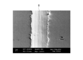
- Test Example 4 is an SEM image obtained by photographing the alignment layer of the oxide superconducting wire 4;
- Sample No. in Test Example 4 is a diagram showing a CeO 2 cap layer 4, which is an image obtained by an electron beam backscatter diffraction method.
- FIG. Sample No. in Test Example 5, no. 6 is a graph showing measurement results of magnetization loss of No. 6.
- FIG. Sample No. in Test Example FIG. 5 is a diagram showing 5 (two-divided wire rods), and is an image obtained by photographing by magneto-optical observation.
- Sample No. in Test Example FIG. 6 is a diagram showing 6 (undivided wire rod), and is an image obtained by photographing by magneto-optical observation.
- Sample No. in Test Example 5, no. 6 is a graph showing measurement results of AC loss of 6;
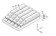
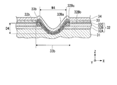
- FIG. 1A is a cross-sectional perspective view showing an oxide superconducting wire 5 according to this embodiment.
- FIG. 1B is a schematic cross-sectional view showing the oxide superconducting wire 5 according to the present embodiment.
- an oxide superconducting wire 5 according to this embodiment has an intermediate layer 2, an oxide superconducting layer 3, and a metal stabilizing layer 4 laminated in this order on a substrate 1.
- non-oriented regions 2 b and 3 b are formed in the intermediate layer 2 and the oxide superconducting layer 3 of the oxide superconducting wire 5.
- first concave groove portions 1a On the main surface 1b of the base material 1, a plurality of first concave groove portions 1a arranged in parallel at intervals are formed.
- the first groove portion 1a functions as an orientation inhibition region. Thereby, the orientation of the intermediate layer 2 and the oxide superconducting layer 3 formed on the first concave groove portion 1a is inhibited, and the intermediate layer 2 and the oxide superconducting layer 3 formed on the first concave groove portion 1a are inhibited.
- non-oriented regions 2b and 3b are formed. Since the non-oriented region 3b of the oxide superconducting layer 3 does not have superconducting properties, it becomes a high resistance region during use, and current does not flow easily.
- the oxide superconducting layer 3 is divided by the non-oriented region 3b, the oxide superconducting layer 3 is substantially divided into two or more wires, and the oxide superconducting layer 3 is thinned.
- the oxide superconducting wire 5 has a configuration (multifilament structure) divided into a plurality of parallel filaments 10 (multifilaments).
- the non-oriented region means a region that does not show orientation in a layer including a region where the crystal shows orientation.
- the orientation-inhibiting region is a region that inhibits the crystal orientation of the layer laminated thereon. Note that the orientation-inhibiting region also inhibits the orientation of a layer stacked via another layer.
- the base material 1 is a base material which can be used as a base material of a superconducting wire, the type of the base material is not limited.
- the substrate 1 is preferably formed of a metal having heat resistance.
- a material of the base material 1 among heat resistant metals, an alloy is preferable, and a nickel (Ni) alloy or a copper (Cu) alloy is more preferable.
- Hastelloy (trade name, manufactured by Haynes Co., Ltd.) is suitable, and the amount of components such as molybdenum (Mo), chromium (Cr), iron (Fe), cobalt (Co) is different.
- the substrate 1 an alignment substrate in which the orientation of metal crystals is uniform may be used.
- the shape of the substrate 1 is a long tape shape, but may be a sheet shape, for example.
- the thickness of the substrate 1 may be appropriately adjusted according to the purpose, and can be in the range of 10 to 500 ⁇ m.
- a plurality of first concave grooves (orientation-inhibiting regions) 1a are formed on the main surface 1b of the substrate 1 and are arranged in parallel at intervals.
- the first concave groove portion 1 a is a V-shaped groove formed on the main surface 1 b of the substrate 1, and extends linearly in the longitudinal direction in the longitudinal direction of the substrate 1. It is preferable that the depth D of the first concave groove portion 1a is 0.3 ⁇ m or more and 10 ⁇ m or less, and the width W1 is 10 ⁇ m or more and 500 ⁇ m or less.
- the non-oriented region 2b can be formed in the intermediate layer 2 of the portion formed on the first concave groove portion 1a. Moreover, the intensity
- the width W1 of the first concave groove portion 1a is 10 ⁇ m or more, the non-oriented region 2b having a sufficient width can be formed.
- the width W1 of the first concave groove portion 1a is a V-shaped groove, but the shape of the groove is not limited thereto. The shape of the groove is not limited as long as it can form the non-oriented region 2b in the intermediate layer 2.
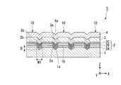
- the intermediate layer 2 is formed on the main surface 1b of the substrate 1.
- a structure in which the base layer 2A, the alignment layer 2B, and the cap layer 2C are laminated in this order can be applied.
- the underlayer 2A is composed of one or both of a diffusion prevention layer and a bed layer.
- the diffusion prevention layer is A part of the constituent elements of the material 1 has a function of suppressing diffusion and mixing into the oxide superconducting layer 3 side as impurities.
- the diffusion prevention layer is made of Si 3 N 4 , Al 2 O 3 , GZO (Gd 2 Zr 2 O 7 ), etc., and is formed to a thickness of 10 to 400 nm, for example.
- the bed layer is provided in order to suppress the reaction of constituent elements at the interface between the base material 1 and the oxide superconducting layer 3 and to improve the orientation of the layer provided above the bed layer (upper surface of the bed layer).
- the bed layer is a layer for reducing interfacial reactivity and obtaining orientation of a film formed on the bed layer.
- the bed layer is made of Y 2 O 3 , CeO 2 , DY 2 O 3 , Er 2 O 3 , Eu 2 O 3 , Ho 2 O 3 , La 2 O 3, etc., and the bed layer has a thickness of, for example, 10 to 100 nm.
- the orientation layer 2B is provided to control the crystal orientation of the cap layer 2C and the oxide superconducting layer 3 formed on the orientation layer 2B.
- the orientation layer 2B is formed of a biaxially oriented material for controlling the crystal orientation of the cap layer 2C formed on the orientation layer 2B.
- As the material of the alignment layer 2B Gd 2 Zr 2 O 7 , MgO, ZrO 2 —Y 2 O 3 (YSZ), SrTiO 3 , CeO 2 , Y 2 O 3 , Al 2 O 3 , Gd 2 O 3 , Zr Examples thereof include metal oxides such as 2 O 3 , Ho 2 O 3 and Nd 2 O 3 .
- the alignment layer 2B is preferably formed by an IBAD (Ion-Beam-Assisted Deposition) method.
- the cap layer 2C is provided to control the crystal orientation so that the crystal orientation of the oxide superconducting layer 3 is equal to or higher than that of the orientation layer 2B.
- the cap layer 2 ⁇ / b> C is formed of a material that can be formed on the surface of the above-described alignment layer 2 ⁇ / b> B so that crystal grains can self-orient in the in-plane direction.
- As the material of the cap layer 2C specifically, CeO 2, Y 2 O 3 , Al 2 O 3, Gd 2 O 3, ZrO 2, YSZ, Ho 2 O 3, Nd 2 O 3, LaMnO 3 etc. Can be mentioned.
- the cap layer 2C can be formed so that the film thickness of the cap layer 2C is in the range of 50 to 5000 nm.
- the intermediate layer is composed of a plurality of layers without using the IBAD method.
- the orientation layer 2B and the cap layer 2C are provided in order to control the orientation of the oxide superconducting layer 3 formed on the cap layer 2C. Since the alignment layer 2B and the cap layer 2C have orientation, the orientation of the oxide superconducting layer 3 formed on the orientation layer 2B and the cap layer 2C can be controlled. Therefore, when the alignment layer 2B and the cap layer 2C do not have the orientation, the oxide superconducting layer 3 formed on the alignment layer 2B and the cap layer 2C cannot have the orientation.
- the orientation of the intermediate layer 2 depends on the surface properties of the main surface 1b of the substrate 1 on which the intermediate layer 2 is laminated.
- the crystal growth direction is disturbed in the layer of the intermediate layer 2, and an orientation suitable for the base of the oxide superconducting layer 3 is obtained.
- the intermediate layer 2 the non-oriented area
- groove part 1a is formed in the part formed on the 1st ditch
- the intermediate layer 2 formed on the first groove portion 1a has the second groove portion 2a formed on the surface of the first groove portion 1a so as to transfer the first groove portion 1a.
- the 2nd groove part 2a becomes a V-shaped groove
- the first concave groove portion 1a of the substrate 1 When the depth D of the first concave groove portion 1a of the substrate 1 is shallow with respect to the thickness of the intermediate layer 2, the first concave groove portion 1a is embedded by stacking the intermediate layer 2, and is formed on the surface of the intermediate layer 2.
- the second concave groove 2a may not be formed. Even in this case, if the non-oriented region 2 b is formed on the surface of the intermediate layer 2, the non-oriented region 3 b can be formed in the oxide superconducting layer 3.
- the oxide superconducting layer 3 As a material for forming the oxide superconducting layer 3, a known material is selected as an oxide superconductor, and specifically, REBa 2 Cu 3 O 7-X (RE is a rare earth element) called RE-123 series. , Y, La, Ce, Pr, Nd, Pm, Sm, Eu, Gd, Tb, Dy, Ho, Er, Tm, Yb, and Lu. Examples of the oxide superconducting layer 3 include Y123 (YBa 2 Cu 3 O 7-X ) and Gd123 (GdBa 2 Cu 3 O 7-X ).
- the oxide superconducting layer 3 has a thickness of about 0.5 to 5 ⁇ m and preferably a uniform thickness.
- a portion formed on the non-oriented region 2 b of the intermediate layer 2 becomes a non-oriented region 3 b in which the crystal orientation is disturbed.
- a third groove 3a is formed so as to transfer the second groove 2a of the intermediate layer 2.
- the orientation of the oxide superconducting layer 3 is controlled by the intermediate layer 2 (particularly, the orientation layer 2B and the cap layer 2C). Therefore, the portion formed on the non-oriented region 2b of the intermediate layer 2 does not have sufficient crystal orientation to develop a superconducting state.
- a linear second concave groove 2a that is a V-shaped groove is formed on the surface of the non-oriented region 2b of the intermediate layer 2.
- the orientation of the oxide superconducting layer 3 depends not only on the orientation of the intermediate layer 2 but also on the surface properties of the intermediate layer 2. As described above, since the second groove portion 2a is formed on the non-oriented region 2b of the intermediate layer 2, the crystals constituting the oxide superconducting layer 3 formed on the second groove portion 2a are more oriented. It becomes difficult to do. Even when the second concave groove 2a is not formed on the surface of the intermediate layer 2, if the non-oriented region 2b is formed, the oxide superconducting layer 3 formed thereon is also non-coated. An alignment region 3b is formed. However, the non-orientation property of the non-orientation region 3b of the oxide superconducting layer 3 becomes remarkable due to the formation of the second concave groove 2a.
- This non-oriented region 3b does not have superconducting characteristics or has a remarkably low critical current due to the disordered orientation. Therefore, when a current is passed through the oxide superconducting wire 5 at a very low temperature, the current hardly flows in the non-oriented region 3b, and the oxide superconducting layer 3 is substantially divided. Since the oxide superconducting layer 3 is partitioned in the width direction by the non-oriented region 3b, the oxide superconducting layer 3 is divided into thin superconductor wires (multifilaments) divided by the non-oriented region 3b. Function.
- the non-oriented region 3b may not be formed on the entire portion on the second groove portion 2a as long as it is formed so as to partition the oxide superconducting layer 3 in the width direction. That is, the non-oriented region 3b may be partially widened or narrowed as long as the current between the highly oriented oxide superconducting layers 3 adjacent to each other across the non-oriented region 3b can be inhibited.
- the metal stabilization layer (protective layer) 4 is formed of a material having good electrical conductivity such as Ag or an Ag alloy.
- the metal stabilizing layer 4 is formed as a layer having a low contact resistance with respect to the oxide superconducting layer 3 and being familiar to the oxide superconducting layer 3.
- the metal stabilizing layer 4 is laminated by a film forming method such as sputtering, and the thickness of the metal stabilizing layer 4 is about 1 to 30 ⁇ m.
- a fourth groove portion 4 a is formed so as to transfer the third groove portion 3 a of the oxide superconducting layer 3.
- stacked on the layer (protective layer) of Ag or an Ag alloy may be employ
- a metal tape or a plating layer may be further laminated on the protective layer.
- a metal tape may be laminated on the metal stabilizing layer 4 or around the oxide superconducting wire 5 via a solder layer.
- a relatively inexpensive conductive metal material such as copper, a copper alloy such as a Cu—Zn alloy, a Cu—Ni alloy, aluminum, an aluminum alloy, or stainless steel can be used.
- the laminated metal tape functions as a bypass for commutating the current of the oxide superconducting layer 3 together with the metal stabilizing layer 4 when the oxide superconducting layer 3 attempts to transition from the superconducting state to the normal conducting state.
- the thickness of the metal tape can be, for example, 10 to 300 ⁇ m. Even when a plating layer such as copper is formed around the oxide superconducting wire 5, the same function as that obtained when the metal tape is used is obtained.
- the configuration of the metal stabilization layer can be applied to other embodiments.
- the oxide superconducting wire 5 may be further covered with an insulating coating layer (not shown). By covering the oxide superconducting wire 5 with the coating layer, the entire oxide superconducting wire 5 is protected, and the oxide superconducting wire 5 having stable performance can be obtained.
- the coating layer is preferably formed of a known material such as various resins or oxides that are usually used for insulating coating such as oxide superconducting wire. Specific examples of the resin include polyimide resin, polyamide resin, epoxy resin, acrylic resin, phenol resin, melamine resin, polyester resin, silicon resin, silicon resin, alkyd resin, and vinyl resin. Moreover, an ultraviolet curable resin is preferable.
- the thickness of the coating by the coating layer is not particularly limited, and may be appropriately adjusted according to the site to be coated.
- the coating layer may be formed by a known method according to the material of the coating layer.
- the coating layer may be formed by applying a raw material on the oxide superconducting wire 5 and curing the coating film. Further, when a sheet-like coating is available, the sheet-like coating may be used and laminated on the oxide superconducting wire 5.
- the oxide superconducting layer 3 of the oxide superconducting wire 5 is formed with a plurality of non-oriented regions 3b extending in parallel at intervals.
- the oxide superconducting layer 3 is divided by the non-oriented region 3b, and the oxide superconducting wire 5 is divided into a plurality of filaments 10.
- each filament 10 is not mechanically divided, a current flows through each filament 10 in the superconducting state because the non-oriented region 3 b is formed in the oxide superconducting layer 3.
- the oxide superconducting wire 5 has a configuration in which a plurality of individual superconducting wires (filaments 10) are arranged in parallel.
- first concave grooves 1a that is, the number of non-oriented regions 2b and 3b formed thereon
- the number of filaments 10 formed on the oxide superconducting wire 5 is increased, and the number is reduced.
- the AC loss decreases as the number increases.
- the shielding current and the magnetization loss due to the shielding current are reduced. This is because when the oxide superconducting layer 3 is divided in the width direction, the amount of movement of the magnetic flux that enters each filament 10 decreases according to the number of divisions. Therefore, it is preferable to form the first concave groove portions 1a formed in a linear shape by increasing the number thereof.
- the width of the filament 10 is too thin, the proportion of the non-oriented region 3b in the oxide superconducting layer 3 increases, and the critical current density is lowered. Further, in this case, in the oxide superconducting layer 3, the non-oriented regions 3b adjacent to each other are connected to each other, and there is a possibility that current does not flow in the length direction. Therefore, it is preferable that the width of the filament 10 divided by the non-oriented regions 2b and 3b formed on the first groove portion 1a and the first groove portion 1a of the substrate 1 is 100 ⁇ m or more. In addition, although the width
- the oxide superconducting layer 3 is divided and thinned by the non-oriented region 3b, thereby reducing the shielding current of the oxide superconducting wire 5 and the magnetization loss due to the shielding current and the AC loss.
- the oxide superconducting wire 5 is divided into a plurality of filaments 10 by forming a plurality of linear non-oriented regions 3 b.
- the resistance between filaments per 1 cm length between the oxide superconducting layers 3 is 1 ⁇ / cm or more.
- the metal stabilization layer 4 may be divided along the third groove 3a.
- a metal stabilizing layer 4 can be formed, for example, by performing masking on the metal stabilizing layer 4, removing the masking of the portion corresponding to the third concave groove portion 3a, and performing etching. Thereby, the part corresponding to the 3rd ditch
- the manufacturing method of the oxide superconducting wire 5 according to the present embodiment includes a step of forming the first groove portion 1 a in the base material 1. A specific manufacturing method will be described below.
- a tape-like base material 1 is prepared, and the main surface 1b of the base material 1 is polished so that the arithmetic average roughness Ra of the main surface 1b is 3 nm to 4 nm. Further, the main surface 1b of the substrate is degreased and washed with acetone. By passing through the above process, the main surface 1b of the base material 1 is prepared so that the orientation of the intermediate layer 2 can be easily obtained when the intermediate layer 2 is laminated.
- FIG. 2 is a schematic view showing a first groove processing device 9 for forming the first groove 1a on the main surface 1b of the substrate 1 in the present embodiment.
- the first groove processing device 9 is generally configured by a feed reel 6, a take-up reel 7, a relay reel 8 ⁇ / b> A disposed between the feed reel 6 and the take-up reel 7, and a processing tool 8. ing.
- the substrate 1 is wound around a delivery reel 6.
- a transport device such as a motor (not shown) is attached to the take-up reel 7.
- the base material 1 is sent out from the reel 6, and the base material 1 is taken up by the take-up reel 7 via the relay reel 8A. be able to.
- the processing tool 8 is a cutting tool for metal processing in which the tip of the processing tool 8 is directed to the relay reel 8A.
- the tip of the processing tool 8 has a sharp V shape, for example. While winding the base material 1 on the take-up reel 7, the tip of the processing tool 8 is pressed against the base material 1 conveyed along the outer periphery of the relay reel 8A. 1 groove 1a, see FIGS. 1A and 1B).
- a plurality of the processing tools 8 in the depth direction (X-axis direction) in FIG. 2, a plurality of first concave grooves 1 a parallel to the longitudinal direction of the tape-shaped substrate 1 can be formed. .
- the intermediate layer 2 is laminated by a conventionally known method on the oxide superconducting wire 5 in which the first concave groove portion 1a is formed (after the formation of the orientation-inhibiting region, the main surface of the base material).
- the intermediate layer composed of one or two or more layers is laminated on the top and the orientation-inhibiting region).
- an oxide superconducting layer 3 is laminated on the main surface of the intermediate layer 2 (an oxide superconducting layer whose crystal orientation is controlled by the intermediate layer is laminated on the intermediate layer).
- a non-oriented region 2b having no orientation is formed on the first concave groove portion 1a.
- the non-oriented region 3b of the oxide superconducting layer 3 is formed on the non-oriented region 2b of the intermediate layer 2 (the oxide located above the orientation-inhibiting region).
- a non-oriented region is formed in the superconducting layer).
- the oxide superconducting layer 3 is subjected to mechanical processing such as laser or chemical processing such as etching. Not. For this reason, the superconducting characteristics in regions other than the alignment region of the oxide superconducting layer 3 are not deteriorated. For the same reason, the peel resistance (peel strength) of each layer does not deteriorate.
- FIG. 3 is a cross-sectional view showing the oxide superconducting wire 15 according to the second embodiment.
- the oxide superconducting wire 15 will be described with reference to FIG.
- the oxide superconducting wire 15 according to the second embodiment is different from the oxide superconducting wire 5 according to the first embodiment in terms of the configuration of the alignment inhibition region.
- the oxide superconducting wire 15 has an intermediate layer 12 (underlying layer 12A, alignment layer 12B, cap layer 12C), oxide superconducting layer 13 and metal stabilizing layer 14 on a base material 11. They are stacked in order. Further, non-oriented regions 12b and 13b are formed in the intermediate layer 12 and the oxide superconducting layer 13 of the oxide superconducting wire 15.
- a plurality of first ridges (orientation-inhibiting regions) 11 a arranged in parallel at intervals are formed on the main surface 11 b of the base material 11.
- line part 11a is the fixing agent 16 adhered and solidified to the main surface 11b of the base material 11 linearly.
- the fixing agent 16 for example, a heat-resistant adhesive that can withstand heat during film formation or heat treatment can be used.
- the fixing agent 16 may be formed using a material such as a heat-resistant ink that is solidified by drying.
- line part 11a it is not limited to the protruding item
- the height H of the first protrusion 11a is 0.3 ⁇ m or more and 10 ⁇ m or less, and the width W2 is 10 ⁇ m or more and 500 ⁇ m or less.
- the non-oriented region 12b can be formed in the portion of the intermediate layer 12 formed on the first ridge portion 11a.
- middle layer 12 can be reduced under the influence of the 1st protruding item
- the non-oriented region 12b By setting the width W2 of the first ridge portion 11a to 10 ⁇ m or more, the non-oriented region 12b having a sufficient width can be formed. Further, by setting the width W2 of the first ridge portion 11a to 500 ⁇ m or less, the width of the non-oriented region 13b of the oxide superconducting layer 13 can be narrowed to ensure the critical current density.
- a non-oriented region 12 b is formed in a portion formed on the first ridge 11 a. This is because the 1st protruding item
- line part 11a forms the 2nd protruding item
- line part 12a is raised and formed in linear form similarly to the 1st protruding item
- the oxide superconducting layer 13 a portion formed on the non-oriented region 12b of the intermediate layer 12 becomes a non-oriented region 13b having no orientation. Since the orientation of the oxide superconducting layer 13 is controlled by the intermediate layer 12 (particularly, the orientation layer 12B and the cap layer 12C), the portion formed on the non-orientation region 12b of the intermediate layer 12 has orientation. I can't. In addition, a linear second ridge 12a is formed on the surface of the non-oriented region 12b of the intermediate layer 12. The orientation of the oxide superconducting layer 13 depends not only on the orientation of the intermediate layer 12 but also on the surface properties of the intermediate layer 12. For this reason, the oxide superconducting layer 13 formed on the second ridge 12a (particularly the step) is more difficult to be oriented.
- the oxide superconducting layer 13 is substantially divided by the non-oriented region 13b. Thereby, the oxide superconducting wire 15 is divided into a plurality of filaments 20, and the plurality of filaments 20 are arranged in parallel. As described above, the oxide superconducting layer 13 is divided by the non-oriented region 13b and the oxide superconducting layer 13 is thinned, so that the shielding current of the oxide superconducting wire 15 and the magnetization loss due to the shielding current and the alternating current are reduced. Loss is reduced.
- FIG. 4 is a schematic diagram showing the first ridge portion processing device 19 that forms the first ridge portion 11a on the main surface 11b of the base material 11 in the present embodiment.
- the first ridge portion processing device 19 is generally composed of a feed reel 6, a take-up reel 7, and a coating portion 18.
- the first ridge processing device 19 applies the fixing agent 16 to be the first ridge 11 a to the substrate 11 by the application unit 18 while winding the substrate 11 on the take-up reel 7.
- line part 11a can be formed in linear form.
- the configuration of the application unit 18 may be configured such that a nozzle is formed at the tip and the nozzle is ejected by an ink jet method. Moreover, it is good also as a structure which sprays material toward the base material 11 with a spray method, masking the part which does not apply
- the intermediate layer 12 is laminated by a conventionally known method on the oxide superconducting wire 15 having the first ridges 11a (lamination step).
- the oxide superconducting layer 13 is laminated on the main surface of the intermediate layer 12.
- the non-oriented region 12b is formed in the intermediate layer 12
- the non-oriented region 13b is formed in the oxide superconducting layer 13
- the oxide superconducting layer 13 is divided into a plurality of filaments 20 by the non-oriented region 13b.
- the produced oxide superconducting wire 15 can be produced.
- the oxide superconducting layer 13 is subjected to mechanical processing by laser or the like, or chemical processing by etching or the like. Not. For this reason, the superconducting characteristics in regions other than the alignment region of the oxide superconducting layer 13 are not deteriorated. For the same reason, the peel resistance (peel strength) of each layer does not deteriorate.
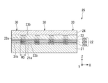
- FIG. 5 is a cross-sectional view showing an oxide superconducting wire 25 according to the third embodiment.
- the oxide superconducting wire 25 will be described with reference to FIG.
- the oxide superconducting wire 25 according to the third embodiment is different from the oxide superconducting wire 5 according to the first embodiment in the configuration of the alignment inhibition region.
- the oxide superconducting wire 25 has an intermediate layer 22 (underlying layer 22A, alignment layer 22B, cap layer 22C), oxide superconducting layer 23, and metal stabilizing layer 24 on a base material 21. They are stacked in order.
- a plurality of first rough surface portions (orientation-inhibiting regions) 21a arranged in parallel with an interval are formed on the main surface 21b of the substrate 21.
- the first rough surface portion 21a is a region having an arithmetic surface roughness Ra of 5 nm to 1000 nm.
- the main surface of the substrate 21 other than the first rough surface portion 21a is polished so that the arithmetic average roughness Ra is about 3 nm to 4 nm.
- the width W3 of the first rough surface portion 21a is preferably 10 ⁇ m or more and 500 ⁇ m or less.
- the non-oriented region 22b can be formed in the portion of the intermediate layer 22 formed on the first rough surface portion 21a.
- the width W3 of the first rough surface portion 21a can be set to 500 ⁇ m or less.
- Such a 1st rough surface part 21a can be formed by laser irradiation with respect to the main surface 21b of the base material 21, for example.
- the processing tool 8 is replaced with a laser irradiation apparatus, and the main surface 21b of the base material 21 is irradiated with laser light to melt and resolidify the main surface 21b.
- the first rough surface portion 21a can be formed on the main surface 21b.
- the first rough surface portion 21a functions as an orientation-inhibiting region.
- a non-oriented region 22b is formed in the intermediate layer 22 formed on the first rough surface portion 21a.
- the second rough surface portion 22a is formed on the surface of the non-oriented region 22b formed on the first rough surface portion 21a. Similar to the first rough surface portion 21a, the second rough surface portion 22a is formed in a linear shape.
- a portion formed on the non-oriented region 22b of the intermediate layer 22 becomes a non-oriented region 23b having no orientation. Since the orientation of the oxide superconducting layer 23 is controlled by the intermediate layer 22 (particularly the orientation layer 22B and the cap layer 22C), the portion formed on the non-orientation region 22b of the intermediate layer 22 has orientation. I can't. In addition, a second rough surface portion 22 a is formed on the surface of the non-oriented region 22 b of the intermediate layer 22. Therefore, the oxide superconducting layer 23 formed on the non-oriented region 22b becomes the non-oriented region 23b.
- the oxide superconducting layer 23 is substantially divided by the non-oriented region 23b. Thereby, the oxide superconducting wire 25 is divided into a plurality of filaments 30 and arranged in parallel. As described above, the oxide superconducting layer 23 is divided by the non-orientation region 23b and the oxide superconducting layer 23 is thinned, whereby the shielding current of the oxide superconducting wire 25, the magnetization loss due to the shielding current, and the AC Loss is reduced.
- the oxide superconducting wire 25 In the oxide superconducting wire 25 according to the present embodiment, after the oxide superconducting layer 23 is laminated, mechanical processing by a laser or the like or chemical processing by etching or the like is not performed. For this reason, the superconducting characteristics in regions other than the alignment region of the oxide superconducting layer 23 are not deteriorated. For the same reason, the peel resistance (peel strength) of each layer does not deteriorate.
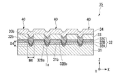
- FIG. 6A is a cross-sectional view showing an oxide superconducting wire 35 according to the fourth embodiment.
- FIG. 6B is an enlarged view of the non-oriented region 33 b of the oxide superconducting layer 33.
- the oxide superconducting wire 35 will be described with reference to FIGS. 6A and 6B.
- the oxide superconducting wire 35 according to the fourth embodiment is different from the oxide superconducting wire 5 according to the first embodiment in the configuration of the groove 32Ba.
- the oxide superconducting wire 35 is formed on the main surface 31b of the base material 31 with the intermediate layer 32 (underlayer 32A, alignment layer 32B, cap layer 32C), oxide superconducting layer 33, and The metal stabilizing layer 34 is laminated in this order (the intermediate layer composed of one or more layers is laminated on the main surface of the base material).
- a concave groove 32Ba reaching the inside of the intermediate layer or the base material 31 is formed on the main surface 32Bb of the alignment layer 32B constituting the intermediate layer 32.
- the concave groove portions 32Ba extend in parallel at intervals.
- the concave groove portion 32Ba can be formed by pressing the processing tool against the main surface 32Bb of the alignment layer 32B and moving the base material 31.
- the method for forming the groove 32Ba is the same as the method for forming the first groove 1a according to the first embodiment.
- a raised portion 32Bc in which the alignment layer 32B is raised is formed at the edge of the concave groove portion 32Ba.
- a part of the material constituting the alignment layer 32B, the base layer 32A, and the base material 31 pressed by the processing tool is recessed. It is formed by escaping to the outside of the groove 32Ba.
- the alignment layer 32B has no orientation in the concave groove portion 32Ba and the raised portion 32Bc. That is, the region where the recessed groove portion 32Ba and the raised portion 32Bc are formed functions as a non-oriented region. Further, the recessed groove portion 32Ba and the raised portion 32Bc function as an alignment inhibition region that inhibits the orientation of the oxide superconducting layer 33 laminated on the recessed groove portion 32Ba and the raised portion 32Bc.
- the width W4 of the recessed groove portion 32Ba is preferably 0.3 ⁇ m or more and 40 ⁇ m or less.
- the width W4 of the groove 32Ba is preferably 0.3 ⁇ m or more and 40 ⁇ m or less.
- the non-oriented region 33b can be reliably formed in the oxide superconducting layer 33.
- the width W4 of the concave groove portion 32Ba is set to 40 ⁇ m or less, the width of the non-oriented region 33b of the oxide superconducting layer 33 can be narrowed to ensure the critical current density.
- the concave groove portion 32Ba means a region where the alignment layer 32B is recessed and is thinner than the film thickness.
- the raised portion 32Bc is not included in the recessed groove portion 32Ba, and is a region formed on both sides of the recessed groove portion 32Ba.
- the width W4 of the recessed groove portion 32Ba does not include the raised portion 32Bc and is the width of the portion where the alignment layer 32B is recessed.
- the depth D4 of the groove 32Ba is a distance in the depth direction from the main surface 32Bb of the alignment layer 32B to the deepest portion of the groove 32Ba.
- the depth D4 of the recessed groove portion 32Ba is preferably 0.3 ⁇ m or more and 10 ⁇ m or less.
- the depth D4 of the groove 32Ba is preferably 0.3 ⁇ m or more and 10 ⁇ m or less.
- the non-oriented region 33b can be reliably formed in the oxide superconducting layer 33.
- strength of the base material 31 is maintainable because the depth D of the ditch
- the cross-sectional shape of the recessed groove portion 32Ba is not limited to the substantially arc shape shown in FIGS. 6A and 6B, and may be, for example, a V-shaped groove.
- the portion of the alignment layer 32B that is stacked on the recessed groove portion 32Ba and the raised portion 32Bc has no orientation.
- the intermediate layer 32 has a non-oriented region 32b as a whole.
- the non-oriented region 32b is a region corresponding to the groove 32Ba and 32Bc located at the edge thereof.
- the portion formed on the non-orientation region 32b of the intermediate layer 32 has orientation. I can't.
- a portion formed on the non-oriented region 32b of the intermediate layer 32 becomes a non-oriented region 33b having no orientation.
- the oxide superconducting layer 33 is substantially divided by the non-oriented region 33b of the oxide superconducting layer 33. Thereby, the oxide superconducting wire 35 is divided into a plurality of filaments 40 and arranged in parallel. As described above, the oxide superconducting layer 33 is divided by the non-orientation region 33b and the oxide superconducting layer 33 is thinned, whereby the shielding current of the oxide superconducting wire 35, the magnetization loss due to the shielding current, and the alternating current. Loss is reduced.
- the oxide superconducting wire 35 according to the fourth embodiment, a part of the intermediate layer 32 that controls the orientation of the oxide superconducting layer 33 is directly processed to form the groove 32Ba. Thereby, the non-oriented region 32b can be reliably formed by the intermediate layer 32.
- the oxide superconducting wire 35 according to the present embodiment is not subjected to mechanical processing by laser or the like or chemical processing by etching or the like after the oxide superconducting layer 33 is stacked. For this reason, the superconducting characteristics in the region other than the alignment region of the oxide superconducting layer 33 are not deteriorated. Further, the peel resistance (peel strength) of each layer does not deteriorate.
- the oxide superconducting layer 33 that is generally laminated has a weak anti-peeling property against the layer located under the oxide superconducting layer 33.
- the peel resistance between the oxide superconducting layer 33 and the intermediate layer 32 located under the oxide superconducting layer 33 can be enhanced. That is, peeling of the oxide superconducting layer 33 can be suppressed.
- the concave groove portion 32Ba of the alignment layer 32B is formed by pressing a processing tool against the main surface 32Bb of the alignment layer 32B, and fine irregularities resulting from the processing are formed on the surface.
- the cap layer 32C formed on the concave groove portion 32Ba having the unevenness fine unevenness is formed on the surface of the cap layer 32C following the fine unevenness formed in the alignment layer 32B.
- the oxide superconducting layer 33 is formed on the cap layer 32C, the bonding strength between the cap layer 32C and the oxide superconducting layer 33 is increased due to the anchor effect caused by fine irregularities, and thus the resistance of the oxide superconducting layer 33 is improved. Peelability increases. Thereby, it is considered that the oxide superconducting layer 33 is hardly peeled off.
- middle layers 32 was illustrated (after laminating
- the recessed groove portion formed in the intermediate layer 32 may be formed on the main surface of any one of the plurality of layers constituting the intermediate layer 32 (laminated layer). Thereby, the concave groove part can constitute the non-oriented region 32 b in the intermediate layer 32.
- the non-orientation region 32 b of the intermediate layer 32 may be a region in which the orientation is disturbed by the concave groove formed in any one of the plurality of layers constituting the intermediate layer 32.
- the concave groove portion 32Ba is covered with the cap layer 32C formed on the alignment layer 32B.
- each layer of the intermediate layer is partially removed, and the base material 31 is exposed, so that the element of the material constituting the base material 31 is likely to diffuse into the oxide superconducting layer 33.
- the cap layer 32C in the groove 32Ba, the base material 31 and the oxide superconducting layer 33 are not in direct contact within the region of the groove 32Ba. Thereby, it can suppress that the metal material which comprises the base material 31 diffuses into the oxide superconducting layer 33. Accordingly, it is preferable that the groove 32Ba is formed in the alignment layer 32B and the groove 32Ba is covered with the cap layer 32C.
- FIG. 7 is a cross-sectional view showing an oxide superconducting wire 45 according to the fifth embodiment.
- the oxide superconducting wire 45 will be described with reference to FIG.
- the configuration of the oxide superconducting wire 45 according to the fifth embodiment is similar to the configuration of the oxide superconducting wire 15 according to the second embodiment.
- the oxide superconducting wire 45 according to the fifth embodiment is different from the oxide superconducting wire 15 according to the second embodiment in terms of the position where the ridge 42a is formed.
- the oxide superconducting wire 45 has an intermediate layer 42 (underlayer 42A, alignment layer 42B, cap layer 42C), oxide superconducting layer 43, and metal stabilization on the main surface 41b of the substrate 41. Layers 44 are stacked in this order. In addition, a non-oriented region 43 b is formed in the oxide superconducting layer 43 of the oxide superconducting wire 45.
- the ridge 42 a is the fixing agent 16 that is linearly attached and solidified on the main surface 41 b of the base material 41.
- the protruding line part 42a is not limited to the protruding line part formed by adhering and solidifying the fixing agent 16, but other forms. You may form the protruding item
- the ridge 42a can be formed by the same method as the formation of the first ridge 11a in the second embodiment.
- the ridge 42a functions as an alignment inhibition region that inhibits the orientation of the oxide superconducting layer 43 laminated on the ridge 42a. Further, the ridge 42a is a part of the intermediate layer 42 and is a non-oriented region made of the fixing agent 16 having no orientation.
- the height H5 of the ridge 42a is preferably 0.3 ⁇ m or more and 10 ⁇ m or less, and the width W5 is preferably 10 ⁇ m or more and 500 ⁇ m or less.
- the non-oriented region 43b can be formed in the portion of the oxide superconducting layer 43 formed on the ridge 42a.
- the height H5 of the ridge 42a is set to 10 ⁇ m or less, the influence on the orientation of the region of the oxide superconducting layer 43 to be crystallized can be reduced due to the influence of the ridge 42a.
- the non-oriented region 43b By setting the width W5 of the protrusion 42a to 10 ⁇ m or more, the non-oriented region 43b having a sufficient width can be formed. In addition, by setting the width W5 of the ridge 42a to 500 ⁇ m or less, the width of the non-oriented region 43b of the oxide superconducting layer 43 can be narrowed to ensure the critical current density.
- the orientation of the oxide superconducting layer 43 is controlled by the intermediate layer 42 (particularly, the orientation layer 42B and the cap layer 42C).
- the portion formed on the ridge 42 a is not directly laminated on the intermediate layer 42, and thus becomes a non-oriented region 43 b having no orientation.
- the oxide superconducting layer 43 is substantially divided by the non-oriented region 43b of the oxide superconducting layer 43.
- the oxide superconducting wire 45 is divided into a plurality of filaments 50, and the plurality of filaments 50 are arranged in parallel.
- the oxide superconducting layer 43 is divided by the non-oriented region 43b, and the oxide superconducting layer 43 is thinned, so that the shielding loss of the oxide superconducting wire 45, the magnetization loss due to the shielding current, and the AC loss are reduced.
- the oxide superconducting wire 45 according to this embodiment is not subjected to mechanical processing by laser or the like or chemical processing by etching or the like after the oxide superconducting layer 43 is stacked. For this reason, the superconducting characteristics in regions other than the alignment region of the oxide superconducting layer 43 are not deteriorated. For the same reason, the peel resistance of each layer does not deteriorate.
- the configuration in which the protruding portion 42a is formed on the main surface 42b of the cap layer 42C in the intermediate layer 42 is exemplified.
- the protrusions 42 a formed on the intermediate layer 42 may be formed on the main surface of any one of the plurality of layers constituting the intermediate layer 42 (laminated layers). Thereby, the protruding portion can constitute the non-oriented region 43 b in the oxide superconducting layer 43.
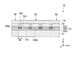
- FIG. 8 shows a cross-sectional view of the oxide superconducting wire 55 according to the sixth embodiment.
- the oxide superconducting wire 55 according to the sixth embodiment is similar to the configuration of the oxide superconducting wire 25 according to the third embodiment.
- the oxide superconducting wire 55 according to the sixth embodiment is different from the oxide superconducting wire 25 according to the third embodiment in that the rough surface portion 52Ba is formed.
- the oxide superconducting wire 55 has an intermediate layer 52 (underlayer 52A, alignment layer 52B, cap layer 52C), oxide superconducting layer 53, and metal stabilization on the main surface 51b of the substrate 51.
- Layers 54 are stacked in this order.
- On the main surface 52Bb of the alignment layer 52B a plurality of rough surface portions (alignment-inhibiting regions) 52Ba arranged in parallel with an interval are formed.
- the rough surface portion 52Ba is a region having an arithmetic surface roughness Ra of 5 nm or more and 1000 nm or less.
- the region where the rough surface portion 52Ba is formed functions as a non-oriented region.
- the rough surface portion 52Ba functions as an orientation-inhibiting region that inhibits the orientation of the layer stacked on the rough surface portion 52Ba.
- the width W6 of the rough surface portion 52Ba is preferably 10 ⁇ m or more and 500 ⁇ m or less.
- the non-oriented region 52b can be formed in the cap layer 52C formed on the rough surface portion 52Ba. Further, in the step of forming the rough surface portion 52Ba, the orientation of the alignment layer 52B is disturbed, and the non-alignment region 52b can be formed also in the alignment layer 52B.
- the width W6 of the rough surface portion 52Ba can be formed by laser irradiation as in the third embodiment.
- the oxide superconducting layer 53 a portion formed on the non-oriented region 52b of the intermediate layer 52 becomes a non-oriented region 53b having no orientation. Since the orientation of the oxide superconducting layer 53 is controlled by the intermediate layer 52 (particularly, the orientation layer 52B and the cap layer 52C), the portion formed on the non-orientation region 52b of the intermediate layer 52 has orientation. I can't. Therefore, the oxide superconducting layer 53 formed on the non-oriented region 52b becomes the non-oriented region 53b.
- the oxide superconducting layer 53 is substantially divided by the non-oriented region 53b of the oxide superconducting layer 53.
- the oxide superconducting wire 55 is divided into a plurality of filaments 60, and the plurality of filaments 60 are arranged in parallel.
- the oxide superconducting layer 53 is divided by the non-oriented region 53b, and the oxide superconducting layer 53 is thinned, thereby reducing the shielding current of the oxide superconducting wire 55, the magnetization loss due to the shielding current, and the AC loss.
- the oxide superconducting layer 53 is not subjected to mechanical processing by laser or the like or chemical processing by etching or the like after the oxide superconducting layer 53 is stacked. For this reason, the superconducting characteristics in regions other than the alignment region of the oxide superconducting layer 53 are not deteriorated. For the same reason, the peel resistance of each layer does not deteriorate.
- middle layers 52 was illustrated.
- the rough surface portion formed in the intermediate layer 52 may be formed on the main surface of any one of the layers constituting the intermediate layer 52. Thereby, the rough surface portion can constitute the non-oriented region 52 b in the intermediate layer 52.
- ⁇ Test Example 1> ⁇ Preparation of sample> First, a tape-shaped base material having a width of 10 mm, a thickness of 0.1 mm, and a length of 1000 mm made of Hastelloy C-276 (trade name of Haynes, USA) was prepared. The main surface of the substrate was polished using alumina having an average particle size of 3 ⁇ m. Next, the surface of the substrate was degreased and washed with acetone.
- the first concave groove portion (concave groove portion) extending in the longitudinal direction of the base material was formed on the main surface of the base material.
- a cutting tool having a thickness of 100 ⁇ m was attached as a processing tool. While the base material is fed out and conveyed from the reel toward the take-up reel, the above-mentioned blade is pressed against the center of the width of the base material to form a scratch extending in the longitudinal direction (V-shaped groove, first concave groove). did.
- the base material was partitioned by a width of 5 mm in the width direction by the concave grooves.
- Al 2 O 3 (diffusion prevention layer; film thickness 100 nm) is formed on the main surface of the base material by sputtering, and Y 2 O 3 (bed layer) is formed on the Al 2 O 3 film by ion beam sputtering. A film thickness of 30 nm) was formed.
- MgO alignment layer; film thickness: 5 to 10 nm
- 500 nm thick is formed on the MgO film by pulsed laser deposition (PLD method).
- CeO 2 (cap layer) was formed.
- a 2.0 ⁇ m thick GdBa 2 Cu 3 O 7-X (oxide superconducting layer) was formed on the CeO 2 layer by the PLD method.
- a metal stabilizing layer made of Ag was formed on the oxide superconducting layer by sputtering, and oxygen annealing was further performed at 500 ° C. for 10 hours, followed by taking out after furnace cooling for 26 hours. Through the above procedure, sample no. 1 oxide superconducting wire was produced.
- sample No. above In the manufacturing procedure of the oxide superconducting wire No. 1, sample No. 1 was obtained by omitting the step of forming the first groove on the main surface of the base material. 2 oxide superconducting wire was produced.
- masking was performed by forming a gap having a width of 100 ⁇ m extending in the longitudinal direction at the center of the width of the wire with a polyimide tape on the surface of the metal stabilizing layer of the wire.
- the metal stabilization layer and the oxide superconducting layer made of GdBa 2 Cu 3 O 7-X are etched using nitric acid to form a groove having a width of 100 ⁇ m in the center of the wire, and the wire is formed into a plurality of wires. Divided and thinned the wire. As a result, sample no. 3 oxide superconducting wire was produced.
- the sample No. 1 was subjected to wire segmentation and multifilamentization (thinning).
- the oxide superconducting wire No. 1 is a sample No. which has not been thinned. Compared with the oxide superconducting wire No. 2, it was possible to reduce the AC loss.
- ⁇ Test Example 2> In the above sample No. In the preparation procedure of oxide superconducting wire No. 1, a sample was prepared by forming a first concave groove having a width of 40 ⁇ m and a depth of 5 ⁇ m on the main surface of the base material, and omitting the film formation of the silver stabilizing layer. A part of the oxide superconducting layer of this sample was removed by etching using nitric acid. Thereafter, an SEM image obtained by photographing this portion (etched portion) is shown in FIG. In FIG. 9, the region located on the left side of the image is the surface of CeO 2 that is the cap layer of the intermediate layer. A region located in the center of the image is a boundary region by etching.
- the region located on the right side of the image is the surface of GdBa 2 Cu 3 O 7-X , which is an oxide superconducting layer.
- GdBa 2 Cu 3 O 7-X which is an oxide superconducting layer.
- the crystal grains of GdBa 2 Cu 3 O 7-X constituting the oxide superconducting layer are exposed. That is, the oxide superconducting layer is in the middle of etching, and the line of the groove is not visible and is interrupted.
- the second groove portion (the second groove portion in FIGS. 1A and 1B) formed on CeO 2 of the intermediate layer (cap layer) corresponding to the first groove portion on the base material with the straight line indicated by the symbol A. 2a). Due to the formation of the second concave groove portion A, a third concave groove portion (corresponding to the third concave groove portion 3a in FIGS. 1A and 1B) appears on the surface of the oxide superconducting layer. It can be confirmed.
- FIG. 10 is an image obtained by an electron beam backscatter diffraction method (EBSD), and shows a crystal orientation state at a position near the second groove A of the CeO 2 cap layer in the above-described sample.
- EBSD electron beam backscatter diffraction method
- the portion shown in dark gray indicates normal good crystal orientation.
- a non-oriented region (corresponding to the non-oriented region 2b in FIGS. 1A and 1B) is formed along the second concave groove portion A. From this, it was confirmed that the non-oriented region was formed in the intermediate layer formed on the concave groove part by forming the concave groove part in the base material.
- the cap layer is crystal-oriented in the width center region C of the second concave groove portion A.
- the reason why the width center region C having crystal orientation is formed is considered as follows.
- a processing tool (corresponding to the processing tool 8 shown in FIG. 2) having a blade with a flat center at the tip was used. Thereby, it is considered that the center of the groove width is formed flat in the first concave groove portion, thereby forming a crystal-oriented portion in the width center region C. As shown in FIG.
- the width central region C is sandwiched between two non-oriented portions, so that the entire oxide superconducting layer Thus, the oxide superconducting layer is divided by the non-oriented region. Therefore, even in such a case, the shielding current, the magnetization loss due to the shielding current, and the AC loss can be reduced.
- sample no. No. 4 oxide superconducting wire was produced.
- Sample No. 4 corresponds to the oxide superconducting wire (FIGS. 6A and 6B) according to the fourth embodiment.
- Sample No. The oxide superconducting wire No. 4 has the above-mentioned sample No.
- the step of forming the concave groove portion on the main surface of the substrate was omitted, and instead, the concave groove portion extending in the longitudinal direction was formed on the main surface of the alignment layer.
- a cutter having a thickness of 100 ⁇ m (the thickness of the blade edge is about 20 ⁇ m) was attached as a processing tool in the concave groove processing apparatus. While feeding the substrate toward the take-up reel from the reel, the blade was pressed against the center of the width of the substrate to form a scratch (concave groove) extending in the longitudinal direction.
- the alignment layer was partitioned by a width of 5 mm in the width direction by the concave grooves.
- the concave groove formed in the alignment layer had a width of about 20 ⁇ m and a depth of about 10 ⁇ m.
- FIG. 4 is an SEM image obtained by photographing the groove portion B formed in the alignment layer 4.
- FIG. 11 is an image obtained by photographing before forming the cap layer and the oxide superconducting layer.
- 12 is an image obtained by electron beam backscatter diffraction (EBSD). 4 shows the crystal orientation state of the cap layer. In FIG. 12, the portion shown in dark gray shows normal good crystal orientation. As shown in FIG. 12, it can be confirmed that a non-oriented region (corresponding to the non-oriented region 32b in FIGS. 6A and 6B) is formed along the groove B. From this, it was confirmed that the non-oriented region was formed in the cap layer formed on the concave groove by forming the concave groove in the alignment layer.
- EBSD electron beam backscatter diffraction
- peel strength Sample No. 4 and sample no.
- the peel strength of the oxide superconducting layer was measured for the oxide superconducting wire 2 (without the groove). The measurement was performed by a stud pull peeling test.
- the tip of the stud pin having a diameter of 2.7 mm is bonded and fixed to the surface of the metal stabilization layer (Ag layer) of each wire constituting the sample with an epoxy resin (adhesion area 5 of the pin tip). 72 mm 2 ). Thereafter, the stud pin was pulled in a direction perpendicular to the upper surface of the wire, and the tensile load at the moment when the stress was reduced was measured as a peeling stress (peeling strength).
- the stud pin was bonded to the center in the width direction of the wire.
- 30 sample Nos. 4 and 30 sample Nos. 2 no groove
- a stud pull peeling test was performed on all the samples.
- 30 sample Nos. 4 and 30 sample Nos. The average value of the measurement results in 2 was calculated. Table 3 shows the calculation results. In each sample, peeling occurred between the oxide superconducting layer and the cap layer.
- Test Example 4 In Test Example 1 described above, a 10 mm wide substrate was used, but in Test Example 4, a 4 mm wide substrate obtained by cutting the side of a 10 mm wide substrate was used as a sample substrate. . In order to obtain a substrate having a width of 4 mm, a substrate having a width of 10 mm was prepared, and the substrate was cut from both sides in the width direction of the substrate to obtain a substrate having a width of 4 mm.
- sample No. 1 in which one concave groove was formed on a substrate having a width of 4 mm. 5 (two-divided wire) and a sample (No. 6) in which no groove was formed were prepared.
- sample no. 5 is a wire material in which a groove portion is formed at the center in the width direction of a base material having a width of 4 mm so as to extend along the extending direction of the base material. That is, sample no.
- Reference numeral 5 denotes a two-divided wire divided by one concave groove.
- Sample No. 6 is a wire material in which no groove is formed in the alignment layer, and is a non-divided wire material.
- Example No. 5, No. 6 a method for creating the sample (Sample No. 5, No. 6) of Test Example 4 will be described.
- the intermediate layer 32 underlayer 32A, alignment layer 32B, cap layer 32C is formed on the main surface 31b of the base 31 having a width of 4 mm.
- An oxide superconducting layer 33 and a metal stabilizing layer 34 were laminated in this order.
- the metal stabilization layer 34 the 2 layer structure of the silver layer and copper layer formed by the sputtering method, and the copper layer formed by the plating method was employ
- the processing tool when forming the intermediate layer 32, the processing tool is pressed against the main surface 32Bb of the alignment layer 32B to move the base material 31, whereby the concave groove portion 32Ba. Formed. Thereafter, a cap layer 32C, an oxide superconducting layer 33, an Ag thin film, and a Cu thin film 34 were sequentially formed on the main surface 32Bb of the alignment layer 32B.
- a wire two-divided wire obtained by forming one concave groove 32Ba in the alignment layer 32B is shown in Sample No. 5 wire.
- a wire rod (non-divided wire rod) that does not form the groove 32Ba in the alignment layer 32B is sample no. 6 wire rod.
- Sample No. In No. 5 since the metal stabilization layer 34 is formed, the plurality of filaments obtained by the division are electrically connected.
- FIG. 13 shows the sample No. in Test Example 4.
- no. 6 is a graph showing measurement results of magnetization loss of No. 6.
- FIG. 13 the horizontal axis indicates a magnetic field B (T) applied from the outside, and the vertical axis indicates magnetization (T).
- T magnetic field B
- T magnetization
- the temperature was 64 K (absolute temperature)
- the magnetization was measured by applying a magnetic field in a direction perpendicular to the oxide superconducting layer while changing the magnetic field so as to have a value shown on the horizontal axis.
- sample no. 5 and sample no. It can be seen that the magnitude relationship with 6 is the same. However, sample No. when the magnetic field is 0 (T). 6 and sample no. The difference from 5 was about 15 (T), but as the magnetic field changed from 0 (T) to about 2,9 (T), or the magnetic field changed from 0 (T) to about -2,9 (T ), The difference decreases. From this, the sample No. in which the groove portion is not formed is shown. 6 and a sample No. in which a groove portion is formed. Compared with FIG. 5, it can be seen that the magnitude (absolute value) of magnetization can be reduced by forming the concave groove in the wire. That is, in the case of two divisions, the magnitude of magnetization can be reduced.
- sample No. No. 7 has a high absolute value of magnetization
- sample No. 5 is sample No. From the result that the absolute value of magnetization is lower than that of Sample No. 6, Sample No. 6 than the shielding current of sample No. 6. It can be seen that the shielding current of 5 is low. That is, sample No. which is a dividing wire. 5 clearly shows that the effect of suppressing the generation of the shielding current can be obtained. From this result, sample No. 5 shows that the magnetization loss can be reduced.
- FIG. 5 is a diagram showing 5 (two-divided wire rods), and is an image obtained by photographing by magneto-optical observation.
- 14B shows a sample No. in the test example.
- FIG. 6 is a diagram showing 6 (undivided wire rod), and is an image obtained by photographing by magneto-optical observation.
- magneto-optical observation it is known that when a superconducting layer is observed with a magnetic field applied to the oxide superconducting layer, the superconducting portion and the non-superconducting portion exhibit different responses.
- Sample No. 1 was obtained by magneto-optical observation utilizing the properties of the superconducting part and the non-superconducting part.
- the layer in which the alignment inhibition region is formed may be any layer of the base material and the intermediate layer. That is, any layer may be used as long as it is a layer formed under the oxide superconducting layer.
Landscapes
- Engineering & Computer Science (AREA)
- Chemical & Material Sciences (AREA)
- Ceramic Engineering (AREA)
- Manufacturing & Machinery (AREA)
- Superconductors And Manufacturing Methods Therefor (AREA)
Abstract
Description
本願は、2014年5月8日に日本に出願された特願2014-96582号及び2014年12月12日に日本に出願された特願2014-251933号に基づき優先権を主張し、その内容をここに援用する。
この酸化物超電導線材を用いた構造の一例として、機械的強度の高い金属製の基材を用い、基材の表面にイオンビームアシスト蒸着法(IBAD法)により結晶配向性の良好な中間層を形成し、中間層の表面に成膜法により酸化物超電導層を形成し、酸化物超電導層の表面にAgなどの良導電材料からなる金属安定化層を形成することで得られる酸化物超電導線材が知られている。
また、遮蔽電流は、時間とともに減衰する。したがって、酸化物超電導線材を時間的に変動しない静磁場を生じさせる超電導装置に適用する場合に、遮蔽電流の減衰により磁場が経時変化してしまうという問題があった。
酸化物超電導線材を複数の線材に分割し、線材を細線化する手法の一例として、線材の上面からその長さ方向に沿ってレーザ光線を照射したり、エッチングするなどして溝を形成し、酸化物超電導層を分断する方法(例えば、特許文献1、特許文献2)等が知られている。
本発明は、上記課題に鑑みなされたものであって、酸化物超電導線材の特性の低下を抑制しつつ遮蔽電流及び遮蔽電流に起因する磁化損失、並びに交流損失を低減した酸化物超電導線材の提供を目的とする。
この構成によれば、中間層が非配向領域を有しているために、酸化物超電導層において非配向領域上に積層された積層部分の配向性が乱れ、酸化物超電導層に非配向領域が形成され、この積層部分は超電導特性を有さない。これにより、酸化物超電導層は非配向領域によって分断されて、酸化物超電導線材が、実質的に、2本以上の線材に分割され(マルチフィラメント化)れ、酸化物超電導線材が細線化されて交流損失が低減される。更に、遮蔽電流及び磁化損失が低減される。
また、このような酸化物超電導線材は、酸化物超電導層の積層後に直接加工を行う必要がないため、酸化物超電導層が損傷して劣化する虞がない。
この構成によれば、配向阻害領域を形成することで、配向阻害領域の上の層に非配向領域を形成することができる。したがって、酸化物超電導層を積層後に直接加工を行う必要がなく、酸化物超電導線材における非配向領域以外の領域における超電導特性が悪化することがない。
この構成によれば、基材又は中間層に凹溝部を形成することで、酸化物超電導線材を容易に複数の線材に分割し、酸化物超電導線材を細線化することができる。
この構成によれば、凹溝部がキャップ層に覆われていることで、基材を形成する金属材料が酸化物超電導層へ拡散することを、キャップ層により抑制できる。これにより、酸化物超電導層の特性劣化を抑制できる。
この構成によれば、基材又は中間層に凸条部を形成することで、酸化物超電導線材を容易に複数の線材に分割し、酸化物超電導線材を細線化することができる。
この構成によれば、基材又は中間層に粗面部を形成することで、酸化物超電導線材を容易に複数の線材に分割し、酸化物超電導線材を細線化することができる。
この構成によれば、容易に、また確実に酸化物超電導層に非配向領域を形成することができる。
上記課題を解決するため、本発明の第3態様に係る酸化物超電導線材の製造方法は、主面を有する基材を準備し、前記基材の前記主面上に、1又は2以上の層からなる中間層を積層し、前記中間層を構成する前記層のうち何れかの層を積層した後に、前記積層された層の主面に、線材の長さ方向に沿って一本又は複数本の配向阻害領域を形成し、前記中間層上及び前記配向阻害領域上に、前記中間層によって結晶配向制御される酸化物超電導層を積層し、前記配向阻害領域の上側に位置する前記酸化物超電導層に非配向領域を形成し、酸化物超電導線材をマルチフィラメント化する。
この構成によれば、基材、又は中間層を構成する前記層のうち何れかの層の主面に配向阻害を形成することで、酸化物超電導層に非配向領域を形成することができる。これにより、酸化物超電導層が非配向領域によって複数に分割され、細線化された(マルチフィラメント化された)酸化物超電導線材を提供することができる。酸化物超電導層は、積層後に直接加工されることがなく酸化物超電導層の配向領域以外の領域における超電導特性が悪化することがない。
この構成によれば、基材又は中間層に凹溝部を形成することで、酸化物超電導線材を容易に複数の線材に分割し、酸化物超電導線材を細線化することができる。
この構成によれば、主面に工具を押し当てて線材を移動させることで、安定した深さ及び幅を有する直線状の凹溝部を容易に形成することができる。直線状の凹溝部は、配向阻害領域として機能するため、酸化物超電導層を非配向領域によって分断して、酸化物超電導線材を複数の線材に分割し、酸化物超電導線材を容易に細線化することができる。なお、中間層に凹溝部を形成する場合には、中間層は凹溝部で配向性が乱されて非配向領域を形成する。
この構成によれば、基材又は中間層に凸条部を形成することで、酸化物超電導線材を容易に複数の線材に分割し、酸化物超電導線材を細線化することができる。
この構成によれば、主面に固着剤を付着させることで、容易に凸条部を形成することができる。この凸条部は、配向阻害領域として機能するため、容易に酸化物超電導線材を複数の線材に分割し、酸化物超電導線材を細線化することができる。
この構成によれば、基材又は中間層に粗面部を形成することで、酸化物超電導線材を容易に複数の線材に分割し、酸化物超電導線材を細線化することができる。
この構成によれば、前記主面にレーザを照射することで、容易に粗面部を形成することができる。この粗面部は、配向阻害領域として機能するため、容易に酸化物超電導線材を複数の線材に分割し、酸化物超電導線材を細線化することができる。なお、中間層に粗面部を形成する場合には、中間層は粗面部で配向性が乱されて非配向領域を形成する。
また、このような酸化物超電導線材は、酸化物超電導層の積層後に直接加工を行う必要がないため、酸化物超電導層が損傷して劣化する虞がない。
まず、第1実施形態について説明する。
図1Aは、本実施形態に係る酸化物超電導線材5を示す断面斜視図である。図1Bは、本実施形態に係る酸化物超電導線材5を示す横断面模式図である。
図1A及び図1Bに示すように、本実施形態に係る酸化物超電導線材5は、基材1上に、中間層2、酸化物超電導層3及び金属安定化層4がこの順に積層されている。また、この酸化物超電導線材5の中間層2及び酸化物超電導層3には、非配向領域2b、3bが形成されている。
酸化物超電導層3の非配向領域3bは、超電導特性を有さないため、使用時には高抵抗領域となり、電流が流れにくくなる。したがって、酸化物超電導層3は非配向領域3bによって分断されるため、実質的に、2本以上の線材に分割され、酸化物超電導層3が細線化される。これにより、酸化物超電導線材5は、並行する複数のフィラメント10(マルチフィラメント)に分割された構成(マルチフィラメント構造)を有する。
基材1は、超電導線材の基材として使用し得る基材であれば、基材の種類は限定されない。基材1は、耐熱性を有する金属で形成されていることが好ましい。基材1の材料としては、耐熱性の金属の中でも、合金が好ましく、ニッケル(Ni)合金又は銅(Cu)合金がより好ましい。なかでも、市販品であれば、ハステロイ(商品名、ヘインズ社製)が好適であり、モリブデン(Mo)、クロム(Cr)、鉄(Fe)、コバルト(Co)等の成分量が異なる、ハステロイB、C、G、N、W等の何れの種類も使用できる。また、基材1として、金属結晶の配向が揃った配向基板を用いても良い。
本実施形態においては、基材1の形状は、長尺のテープ形状であるが、例えば、シート形状であっても良い。基材1の厚みは、目的に応じて適宜調整すれば良く、10~500μmの範囲とすることができる。
第1凹溝部1aの深さDは、0.3μm以上10μm以下、幅W1は、10μm以上500μm以下、とすることが好ましい。
第1凹溝部1aの深さDを0.3μm以上とすることでこの第1凹溝部1a上に形成される部分の中間層2に非配向領域2bを形成することができる。また、第1凹溝部1aの深さDを10μm以下とすることで、基材1の強度を維持することができる。
第1凹溝部1aの幅W1を10μm以上とすることで十分な幅を有する非配向領域2bを形成することができる。また、第1凹溝部1aの幅W1を500μm以下とすることで、酸化物超電導層3の非配向領域3bの幅を狭くして臨界電流密度を確保することができる。
なお、本実施形態において、第1凹溝部1aは、V字状の溝であるとしたが、凹溝部の形状はこれに限られない。中間層2に非配向領域2bを形成することができる溝形状であれば、溝の形状は限定されない。
なお、基材として配向基板を用いる場合は、中間層は、IBAD法を用いずに、複数の層から構成される。
本実施形態においては、基材1の主面1bに第1凹溝部1aが形成され、被成膜面に傾いた面が形成されているため、この第1凹溝部1a上に形成される中間層2の配向が乱れる。これにより、中間層2において、基材1の第1凹溝部1a上に形成される部分には、第1凹溝部1aに対応する非配向領域2bが形成される。また、第1凹溝部1a上に形成される中間層2は、第1凹溝部1aを転写するように、第1凹溝部1aの表面に第2凹溝部2aが形成される。第2凹溝部2aは、第1凹溝部1aと同様に、V字状の溝となる。
酸化物超電導層3の厚みは、0.5~5μm程度であって、均一な厚みであることが好ましい。
酸化物超電導層3は、中間層2(特に配向層2B、キャップ層2C)によって配向性が制御されている。したがって、中間層2の非配向領域2b上に形成された部分は、超電導状態を発現するのに十分な結晶配向性を有さない。
加えて、中間層2の非配向領域2bの表面にはV字状の溝である線状の第2凹溝部2aが形成されている。酸化物超電導層3の配向性は、中間層2の配向性のみならず、中間層2の表面性状にも依存する。このように中間層2の非配向領域2b上に第2凹溝部2aが形成されていることで、第2凹溝部2aの上に形成される酸化物超電導層3を構成する結晶は、より配向しにくくなる。なお、中間層2の表面に第2凹溝部2aが形成されていない場合であっても、非配向領域2bが形成されていれば、その上に形成される酸化物超電導層3にも、非配向領域3bが形成される。しかしながら、第2凹溝部2aが形成されていることで酸化物超電導層3の非配向領域3bの非配向性が顕著となる。
非配向領域3bによって酸化物超電導層3が幅方向に区画されていることによって、酸化物超電導層3は、非配向領域3bによって分割されて細線化された複数本の超電導線(マルチフィラメント)として機能する。
非配向領域3bは、酸化物超電導層3を幅方向に区画するように形成されていれば、第2凹溝部2a上の部分全体に形成されていなくても良い。即ち、非配向領域3bは、非配向領域3bを挟んで隣り合う配向性の高い酸化物超電導層3同士の電流を阻害できれば、部分的に幅が広くなったり狭くなったりしても良い。
金属安定化層4の表面には、酸化物超電導層3の第3凹溝部3aを転写するように、第4凹溝部4aが形成される。
金属安定化層4の上に、あるいは、酸化物超電導線材5の周囲に、半田層を介して金属テープを積層しても良い。この場合、金属テープとしては、銅、Cu-Zn合金、Cu-Ni合金等の銅合金、アルミニウム又はアルミニウム合金、ステンレス等の比較的安価な導電性の金属材料を用いることができる。
積層された金属テープは、酸化物超電導層3が超電導状態から常電導状態に遷移しようとした時、金属安定化層4とともに、酸化物超電導層3の電流を転流するバイパスとして機能する。金属テープの厚さは、例えば、10~300μmとすることができる。酸化物超電導線材5の周囲に銅などのめっき層を形成する場合も、上述の金属テープを用いる場合と同様の機能が得られる。金属安定化層の構成は、他の実施形態に適用できる。
被覆層は、例えば、酸化物超電導線材等の絶縁被覆に通常使用される、各種樹脂や酸化物等の公知の材質で形成されているのが好ましい。
前記樹脂として具体的には、ポリイミド樹脂、ポリアミド樹脂、エポキシ樹脂、アクリル樹脂、フェノール樹脂、メラミン樹脂、ポリエステル樹脂、ケイ素樹脂、シリコン樹脂、アルキッド樹脂、ビニル樹脂等が例示できる。また、紫外線硬化性樹脂が好ましい。
前記酸化物としては、CeO2、Y2O3、Gd2Zr2O7、Gd2O3、ZrO2-Y2O3(YSZ)、Zr2O3、Ho2O3等が例示できる。
被覆層による被覆の厚さは、特に限定されず、被覆対象部位等に応じて、適宜調節すれば良い。
被覆層は、被覆層の材質に応じて公知の方法で形成すれば良く、例えば、原料を酸化物超電導線材5上に塗布して、塗布膜を硬化させて被覆層を形成すれば良い。また、シート状の被覆が入手できる場合には、シート状の被覆を使用して酸化物超電導線材5上に積層しても良い。
したがって、基材1の第1凹溝部1a及び第1凹溝部1aの上に形成される非配向領域2b、3bによって分断されたフィラメント10の幅は、100μm以上とすることが好ましい。
なお、各フィラメント10の幅は、それぞれ互いに同一でも異なっていても良いが、通常はほぼ同一とされる。
酸化物超電導線材5においては、複数の線状の非配向領域3bを形成することにより、酸化物超電導線材5が複数のフィラメント10に分割される。各酸化物超電導層3間の1cm長あたりのフィラメント間の抵抗は、1Ω/cm以上となる。
また、金属安定化層4に金属テープやめっき層を積層する場合においても、金属テープやめっき層を酸化物超電導層3の非配向領域3b上に位置する部分をエッチングなどにより除去してもよい。
このような実施形態においては、各フィラメント10同士が、電気的に接続されないため、遮蔽電流及び遮蔽電流に起因する磁化損失、並びに交流損失をより効果的に低減できる。
本実施形態に係る酸化物超電導線材5の製造方法は、基材1に第1凹溝部1aを形成する工程を有している。以下に具体的な製造方法を説明する。
図2は、本実施形態において、基材1の主面1bに第1凹溝部1aを形成する第1凹溝部加工装置9を示す概略図である。
基材1は、送出しリール6に巻回されている。巻取りリール7には、モータ(図示略)等の搬送装置が取り付けられている。基材1を巻取りリール7に巻き掛けて、搬送装置を動作させることで、基材1を送出しリール6から送り出して、中継リール8Aを介し、基材1を巻取りリール7で巻き取ることができる。
基材1を巻取りリール7に巻き取りながら、加工工具8の先端を、中継リール8Aの外周に沿って搬送される基材1に押し当てることで、基材1に直線状の溝(第1凹溝部1a、図1A及び図1B参照)を形成することができる。
なお、加工工具8を図2の奥行方向(X軸方向)に並べて複数配置することで、テープ状の基材1の長手方向に沿って平行な第1凹溝部1aを複数形成することができる。
さらに金属安定化層4を積層することで、非配向領域3bにより複数のフィラメント10に分割され、細線化された酸化物超電導線材5を作製することができる。
次に、第2実施形態について説明する。
図3は、第2実施形態に係る酸化物超電導線材15を示す断面図である。以下、図3を基に、酸化物超電導線材15について説明する。
第2実施形態に係る酸化物超電導線材15は、配向阻害領域の構成の点で、第1実施形態に係る酸化物超電導線材5とは異なる。
第1凸条部11aの形態として、固着剤16を付着させて固化させることで形成される凸条部に限定されず、他の形態を有する凸条部を形成してもよい。例えば、基材11の主面11bを凹凸形状に加工することで第1凸条部11aを形成しても良い。
第1凸条部11aの高さHを0.3μm以上とすることでこの第1凸条部11a上に形成される部分の中間層12に非配向領域12bを形成することができる。また、第1凸条部11aの高さHを10μm以下とすることで、第1凸条部11aの影響で、中間層12の結晶配向すべき領域の配向性に対する影響を低減できる。
第1凸条部11aの幅W2を10μm以上とすることで、十分な幅を有する非配向領域12bを形成することができる。また、第1凸条部11aの幅W2を500μm以下とすることで、酸化物超電導層13の非配向領域13bの幅を狭くして臨界電流密度を確保することができる。
固着剤16は、基材11の主面11bに付着する異物であるため、固着剤16の上に形成される中間層12は、所定の方向に配向することができなくなる。また、中間層12の配向性は、中間層12が積層される基材11の主面11bの表面性状に依存する。固着剤16からなる第1凸条部11aは、段差を形成するため、中間層12の配向性を乱し、中間層12に非配向領域12bを形成する。
また、第1凸条部11a上に形成される中間層12は、第1凸条部11aを転写するように、第1凸条部11aの表面に第2凸条部12aが形成される。第2凸条部12aは、第1凸条部11aと同様に、線状に盛り上がって形成される。
酸化物超電導層13は、中間層12(特に配向層12B、キャップ層12C)によって配向性が制御されているため、中間層12の非配向領域12b上に形成された部分は配向性を有することができない。加えて、中間層12の非配向領域12bの表面には線状の第2凸条部12aが形成されている。酸化物超電導層13の配向性は、中間層12の配向性のみならず、中間層12の表面性状にも依存する。このため、第2凸条部12aの上(特に段部)に形成される酸化物超電導層13は、より配向しにくくなる。
このように、非配向領域13bによって酸化物超電導層13が分割され、酸化物超電導層13が細線化されることで、酸化物超電導線材15の遮蔽電流及び遮蔽電流に起因する磁化損失、並びに交流損失が低減される。
まず、第1実施形態に係る製造方法と同様に、テープ状の基材11を研磨し、さらに脱脂、洗浄する。
次に、このテープ状の基材11の主面11bに線状の第1凸条部11aを形成する。
図4は、本実施形態において、基材11の主面11bに第1凸条部11aを形成する第1凸条部加工装置19を示す概略図である。
第1凸条部加工装置19は、送出しリール6と巻取りリール7と塗布部18とから概略構成されている。第1凸条部加工装置19は、基材11を巻取りリール7に巻き取りながら、塗布部18によって、第1凸条部11aとなる固着剤16を、基材11に塗布する。これにより、第1凸条部11aを直線状に形成することができる。
塗布部18の構成として、先端にノズルが形成され、インクジェット法により吐出する構成としても良い。また、材料の塗布しない部分をマスクしながら、スプレー法により、材料をスプレー状に基材11に向けて吹きかける構成としても良い。
第1凸条部11aを形成した酸化物超電導線材15に従来公知の方法で、中間層12を積層する(積層工程)。さらに、中間層12の主面に酸化物超電導層13を積層する。これにより、中間層12に非配向領域12bが形成され、酸化物超電導層13に非配向領域13bが形成され、非配向領域13bにより酸化物超電導層13が複数のフィラメント20に分割され、細線化された酸化物超電導線材15を作製できる。
次に、第3実施形態について説明する。
図5は、第3実施形態に係る酸化物超電導線材25を示す断面図である。以下、図5を基に、酸化物超電導線材25について説明する。
第3実施形態に係る酸化物超電導線材25は、配向阻害領域の構成の点で、第1実施形態に係る酸化物超電導線材5とは異なる。
基材21の主面21bには、間隔をおいて平行に配置された複数本の第1粗面部(配向阻害領域)21aが形成されている。この第1粗面部21aは、その算術表面粗さRaが5nm以上1000nm以下とされた領域である。
なお、第1粗面部21a以外の基材21の主面は、算術平均粗さRaが3nm~4nm程度となるように研磨されている。
一例として、図2の第1凹溝部加工装置9において、加工工具8をレーザ照射装置に置き換えて、基材21の主面21bにレーザ光を照射し主面21bを溶融、再固化させることで、主面21bに第1粗面部21aを形成することができる。
また、第1粗面部21a上に形成される非配向領域22bの表面には、第2粗面部22aが形成される。第2粗面部22aは、第1粗面部21aと同様に、線状に形成される。
酸化物超電導層23は、中間層22(特に配向層22B、キャップ層22C)によって配向性が制御されているため、中間層22の非配向領域22b上に形成された部分は配向性を有することができない。加えて、中間層22の非配向領域22bの表面には、第2粗面部22aが形成されている。したがって、非配向領域22b上に形成される酸化物超電導層23は非配向領域23bとなる。
このように、非配向領域23bによって酸化物超電導層23が分割され、酸化物超電導層23が細線化されることで、酸化物超電導線材25の遮蔽電流及び遮蔽電流に起因する磁化損失、並びに交流損失が低減される。
次に、第4実施形態について説明する。
図6Aは、第4実施形態に係る酸化物超電導線材35を示す断面図である。また、図6Bは、酸化物超電導層33の非配向領域33bの拡大図である。以下、図6A及び図6Bを基に、酸化物超電導線材35について説明する。
第4実施形態に係る酸化物超電導線材35は、凹溝部32Baの構成の点で、第1実施形態に係る酸化物超電導線材5とは異なる。
凹溝部32Baの幅W4を0.3μm以上とすることで酸化物超電導層33に確実に非配向領域33bを形成することができる。また、凹溝部32Baの幅W4を40μm以下とすることで、酸化物超電導層33の非配向領域33bの幅を狭くして臨界電流密度を確保することができる。
なお、本明細書において、凹溝部32Baとは、配向層32Bが凹み、成膜厚さより薄くなっている領域を意味する。したがって、隆起部32Bcは、凹溝部32Baに含まれず、凹溝部32Baの両側に形成された領域となる。凹溝部32Baの幅W4は、隆起部32Bcを含まず、配向層32Bが凹んだ部分の幅である。凹溝部32Baの深さD4は、配向層32Bの主面32Bbから凹溝部32Baの最も深い部分までの深さ方向の距離である。
凹溝部32Baの深さD4を0.3μm以上とすることでこの酸化物超電導層33に確実に非配向領域33bを形成することができる。また、凹溝部32Baの深さDを10μm以下とすることで、基材31の強度を維持することができる。
なお、凹溝部32Baの断面形状は、図6A及び図6Bに示された略円弧形状に限られず、例えば、V字状の溝であっても良い。
また、本実施形態に例示したように、配向層32Bに凹溝部32Baを形成することで、凹溝部32Baは、配向層32B上に形成されたキャップ層32Cにより覆われる。配向層32Bに凹溝部32Baを形成する場合、凹溝部32Baに位置する部分である配向層32B、および、その部分の下に位置する中間層の各層が薄くなったりする。あるいは、中間層の各層が、部分的に除去され、基材31が露出したりして、基材31を構成する材料の元素が酸化物超電導層33に拡散しやすくなる。凹溝部32Baにキャップ層32Cを形成することで、凹溝部32Baの領域内で基材31と酸化物超電導層33が直接接触することがない。これにより、基材31を構成する金属材料が、酸化物超電導層33への拡散することを抑制できる。したがって、凹溝部32Baが、配向層32Bに形成され、キャップ層32Cにより凹溝部32Baを覆う構造とすることが好ましい。
次に、第5実施形態について説明する。
図7は、第5実施形態に係る酸化物超電導線材45を示す断面図である。以下、図7を基に、酸化物超電導線材45について説明する。
第5実施形態に係る酸化物超電導線材45の構成は、第2実施形態に係る酸化物超電導線材15の構成と類似している。凸条部42aが形成される位置の点で、第5実施形態に係る酸化物超電導線材45が第2実施形態に係る酸化物超電導線材15とは異なる。
凸条部42aは、凸条部42aの上に積層される酸化物超電導層43の配向性を阻害する配向阻害領域として機能する。また、凸条部42aは、中間層42の一部であり、配向性を持たない固着剤16からなる非配向領域である。
凸条部42aの高さH5を0.3μm以上とすることでこの凸条部42a上に形成される部分の酸化物超電導層43に非配向領域43bを形成することができる。また、凸条部42aの高さH5を10μm以下とすることで、凸条部42aの影響で、酸化物超電導層43の結晶配向すべき領域の配向性に対する影響を低減できる。
凸条部42aの幅W5を10μm以上とすることで、十分な幅を有する非配向領域43bを形成することができる。また、凸条部42aの幅W5を500μm以下とすることで、酸化物超電導層43の非配向領域43bの幅を狭くして臨界電流密度を確保することができる。
次に、第6実施形態について説明する。
図8に、第6実施形態に係る酸化物超電導線材55の断面図を示す。以下、図8を基に、酸化物超電導線材55について説明する。
第6実施形態に係る酸化物超電導線材55は、第3実施形態に係る酸化物超電導線材25の構成と類似している。粗面部52Baが形成される位置の点で、第6実施形態に係る酸化物超電導線材55が第3実施形態に係る酸化物超電導線材25とは異なる。
配向層52Bの主面52Bbには、間隔をおいて平行に配置された複数本の粗面部(配向阻害領域)52Baが形成されている。この粗面部52Baは、その算術表面粗さRaが5nm以上1000nm以下とされた領域である。
中間層52において、粗面部52Baが形成された領域は、非配向領域として機能する。また、粗面部52Baは、粗面部52Baの上に積層される層の配向性を阻害する配向阻害領域として機能する。
粗面部52Baは、第3実施形態と同様に、レーザ照射により形成することができる。
酸化物超電導層53は、中間層52(特に配向層52B、キャップ層52C)によって配向性が制御されているため、中間層52の非配向領域52b上に形成された部分は配向性を有することができない。したがって、非配向領域52b上に形成される酸化物超電導層53は非配向領域53bとなる。
<試料の作製>
まず、ハステロイC-276(米国ヘインズ社商品名)からなる幅10mm、厚み0.1mm、長さ1000mmのテープ状の基材を準備した。基材の主面を平均粒径3μmのアルミナを使用し研磨した。次に、前記基材の表面をアセトンにより脱脂、洗浄した。
次いで、このベッド層上に、イオンビームアシスト蒸着法(IBAD法)によりMgO(配向層;膜厚5~10nm)を形成し、MgO膜の上にパルスレーザー蒸着法(PLD法)により500nm厚のCeO2(キャップ層)を成膜した。次いで、CeO2層上にPLD法により2.0μm厚のGdBa2Cu3O7-X(酸化物超電導層)を形成した。この酸化物超電導層上にスパッタ法によりAgからなる金属安定化層を形成し、さらに500℃で10時間の酸素アニールを行い26時間炉冷後に取り出した。
以上の手順を経て、サンプルNo.1の酸化物超電導線材を作製した。
サンプルNo.1~No.3の酸化物超電導線材を77Kに冷却し、線材の面に対して垂直方向に1Tの磁場を印加した状態で、四端子法を用い各サンプルの交流損失を測定した。
測定結果を表1に示す。

上記のサンプルNo.1の酸化物超電導線材の作製手順において、基材の主面に幅40μm、深さ5μmの第1凹溝部を形成し、銀安定化層の成膜を省いたサンプルを用意した。
このサンプルの酸化物超電導層の一部を、硝酸を用いたエッチングにより、除去した。その後、この部分(エッチングされた部分)を撮影して得られたSEM画像を図9に示す。なお、図9において、画像左側に位置する領域が中間層のキャップ層であるCeO2の表面である。画像中央に位置する領域がエッチングによる境界領域である。画像右側に位置する領域が酸化物超電導層であるGdBa2Cu3O7-Xの表面である。画像中央に位置するエッチングによる境界領域では、酸化物超電導層を構成するGdBa2Cu3O7-Xの結晶粒が表出した状態となっている。即ち、酸化物超電導層がエッチングの途中の状態となっており、凹溝部の線が見えなくなり途切れてしまっている。
試験例2において、基材の主面に第1凹溝部を形成する際に、先端中央が平坦な刃を有する加工工具(図2に示す加工工具8に相当)を使用した。これにより、第1凹溝部に、溝幅中央が平坦に形成され、これにより幅中央領域Cに結晶配向した部分が形成されたと考えられる。
図10に示すように、幅中央領域Cに結晶配向している部分が存在していても、2本の非配向の部分に幅中央領域Cが挟まれているため、酸化物超電導層の全体において非配向の領域によって酸化物超電導層が分断されていることになる。したがって、このような場合であっても遮蔽電流及び遮蔽電流に起因する磁化損失、並びに交流損失を低減できる。
まず、サンプルNo.4の酸化物超電導線材を作製した。サンプルNo.4は、第4実施形態に係る酸化物超電導線材(図6A及び図6B)に対応している。サンプルNo.4の酸化物超電導線材は、上記のサンプルNo.1の酸化物超電導線材の作製手順において、基材の主面に凹溝部を形成する工程を省き、代わりに、配向層の主面に長手方向に延びる凹溝部を形成した。配向層の主面に凹溝部を形成する工程においては、まず、凹溝部加工装置において加工工具として厚さ100μm(刃先の厚さは、約20μm)の刃物を取り付けた。基材を送出しリールから巻取りリールに向けて搬送させながら、上記の刃物を基材の幅中央に押し当てて、長手方向に延びる傷(凹溝部)を形成した。凹溝部によって配向層は幅方向に幅5mmずつに区画された。配向層に形成した凹溝部は、幅が約20μm、深さ約10μmであった。
また、図12は電子線後方散乱回折法(EBSD)によって得られた画像であり、サンプルNo.4におけるキャップ層の結晶配向状態を示している。図12において、濃灰色で示された部分が通常の良好な結晶配向性を示している。図12に示すように、凹溝部Bに沿って非配向領域(図6A及び図6Bの非配向領域32bに対応)が形成されていることが確認できる。このことから、配向層に凹溝部を形成することで、凹溝部の上に形成されるキャップ層に非配向領域が形成されていることが確認された。
サンプルNo.4とサンプルNo.2(凹溝部なし)の酸化物超電導線材を77Kに冷却し、四端子法を用いて、サンプルNo.4及びサンプルNo.2の臨界電流値(Ic)を測定した。サンプルNo.4及びサンプルNo.2の臨界電流値Icを表2に示す。
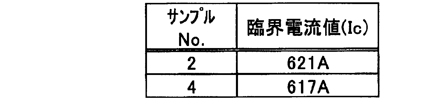
サンプルNo.4とサンプルNo.2(凹溝部なし)の酸化物超電導線材に対し、酸化物超電導層の剥離強度を測定した。
測定は、スタッドプル剥離試験により行った。
スタッドプル剥離試験においては、上記サンプルを構成する各線材の金属安定化層(Ag層)の表面に直径2.7mmのスタッドピンの先端部をエポキシ樹脂で接着固定(ピン先端部の接着面積5.72mm2)した。その後、このスタッドピンを線材の上面に対して垂直方向に引っ張り、応力が低下した瞬間の引張荷重を剥離応力(剥離強度)として測定した。
スタッドピンは、線材の幅方向中心に接着した。
スタッドプル剥離試験において、まず、30個のサンプルNo.4及び30個のサンプルNo.2(凹溝部なし)を準備し、全てのサンプルに対してスタッドプル剥離試験を行った。30個のサンプルNo.4における測定結果の平均値と、30個のサンプルNo.2における測定結果の平均値とを算出した。算出結果を表3に示す。なお、各サンプルにおいて、剥離は、酸化物超電導層とキャップ層との間で生じた。

サンプルNo.4とサンプルNo.2(凹溝部なし)の酸化物超電導線材を77Kに冷却し、サンプルNo.4及びサンプルNo.2の線材の幅方向の抵抗値を計測した。各サンプルの幅方向抵抗値を表4に示す。

上述した試験例1では、10mm幅の基材を用いたが、試験例4では、幅10mmの基材の側部を切断することによって得られた幅4mmの基材をサンプル基材として用いた。幅4mmの基材を得るには、幅10mmの基材を準備し、この基材の幅方向における両側から基材を切断し、幅4mmの基材を得た。
サンプルNo.6は、配向層に凹溝部が形成されていない線材であり、無分割線材である。
上記凹溝部32Baを形成する際に、配向層32Bに1本の凹溝部32Baを形成して得られた線材(2分割線材)がサンプルNo.5の線材である。配向層32Bに凹溝部32Baを形成しない線材(無分割線材)がサンプルNo.6の線材である。
サンプルNo.5においては、金属安定化層34が形成されているので、分割によって得られた複数のフィラメント間が導通している。
図13は、試験例4におけるサンプルNo.5、No.6の磁化損失の測定結果を示すグラフである。図13において、横軸は、外部から印加した磁場B(T)を示しており、縦軸は、磁化(T)を示している。測定条件として、温度は64K(絶対温度)であり、横軸に示す値となるように磁場を変化させながら、酸化物超電導層に垂直な方向に磁場を印加して磁化を測定した。
図14Aは、試験例におけるサンプルNo.5(2分割線材)を示す図であって、磁気光学観察により撮影して得られた画像である。図14Bは、試験例におけるサンプルNo.6(無分割線材)を示す図であって、磁気光学観察により撮影して得られた画像である。
磁気光学観察においては、酸化物超電導層に磁場を印加した状態で酸化物超電導層を観察すると、超電導部分と非超電導部分とは異なる応答を示すことが知られている。このような超電導部分及び非超電導部分の性質を利用した磁気光学観察によってサンプルNo.5(2分割線材)を観察すると、図14Aに示すように、線幅4mmの線材の中央において非超電導部分が観察された。その一方、磁気光学観察によってサンプルNo.6(無分割線材)を観察すると、図14Bに示すように、非超電導部分が観察されず、基材上の全ての領域において超電導部分が観察された。
図15は、試験例4におけるサンプルNo.5、No.6の交流損失の測定結果を示すグラフである。図15において、横軸は、外部から印加した磁場B(T)を示しており、縦軸は、交流損失(AC Loss、J/m3 cycle)を示している。測定条件として、温度は64K(絶対温度)であり、横軸に示す値となるように磁場を変化させながら、酸化物超電導層に垂直な方向に磁場を印加して磁化を測定した。磁化法と呼ばれる算出方法を採用し、測定された磁化の値から交流損失を計算した。交流損失の測定においては、最大印加磁場を横軸にプロットし、1サイクルあたりの損失量を交流損失とし、縦軸にプロットしている。
この結果から、無分割線材のサンプルNo.6の交流損失は、2分割線材のサンプルNo.5の約1.8倍であることが分かる。この結果から、分割線材であるサンプルNo.5においては、交流損失を低減できることが分かる。
Claims (15)
- 基材と、
前記基材の主面上に積層され、配向性を有する1又は2以上の層を有し、線材の長さ方向に沿って延びる一本又は複数本の非配向領域を有する中間層と、
前記中間層上に積層され、前記中間層により結晶配向制御され、前記中間層の前記非配向領域上に位置する非配向領域を有する酸化物超電導層と、を有するマルチフィラメント化された酸化物超電導線材。 - 前記基材の前記主面又は前記中間層を構成する層のうち何れかの層の主面に設けられた配向阻害領域を有し、
前記配向阻害領域は、前記配向阻害領域の上に積層される層の結晶配向性を阻害して前記非配向領域を形成させる領域である、請求項1に記載の酸化物超電導線材。 - 前記配向阻害領域が、前記基材の前記主面又は前記中間層を構成する前記層のうち何れかの層の前記主面に形成された凹溝部である、請求項2に記載の酸化物超電導線材。
- 前記中間層が、配向層と、前記配向層上に積層されたキャップ層と、を有し、
前記キャップ層上に前記酸化物超電導層が積層され、
前記凹溝部が、前記キャップ層により覆われている、請求項3に記載の酸化物超電導線材。 - 前記配向阻害領域が、前記基材の前記主面又は前記中間層を構成する前記層のうち何れかの層の前記主面に形成された凸条部である、請求項2に記載の酸化物超電導線材。
- 前記配向阻害領域が、前記基材の前記主面又は前記中間層を構成する前記層のうち何れかの層の前記主面に形成された粗面部であり、
前記粗面部は、前記粗面部が形成されていない部位より相対的に算術平均粗さRaが大きい領域である、請求項2に記載の酸化物超電導線材。 - 前記粗面部の算術平均粗さRaは、5nm以上1000nm以下である、請求項6に記載の酸化物超電導線材。
- 主面を有する基材を準備し、
前記基材の前記主面に、線材の長さ方向に沿って一本又は複数本の配向阻害領域を形成し、
前記配向阻害領域を形成した後に、前記基材の前記主面上及び前記配向阻害領域上に、1又は2以上の層からなる中間層を積層し、
前記中間層上に、前記中間層によって結晶配向制御される酸化物超電導層を積層し、
前記配向阻害領域の上側に位置する前記酸化物超電導層に非配向領域を形成し、
酸化物超電導線材をマルチフィラメント化する、酸化物超電導線材の製造方法。 - 主面を有する基材を準備し、
前記基材の前記主面上に、1又は2以上の層からなる中間層を積層し、
前記中間層を構成する前記層のうち何れかの層を積層した後に、前記積層された層の主面に、線材の長さ方向に沿って一本又は複数本の配向阻害領域を形成し、
前記中間層上及び前記配向阻害領域上に、前記中間層によって結晶配向制御される酸化物超電導層を積層し、
前記配向阻害領域の上側に位置する前記酸化物超電導層に非配向領域を形成し、
酸化物超電導線材をマルチフィラメント化する、酸化物超電導線材の製造方法。 - 前記配向阻害領域が、凹溝部であり、
前記配向阻害領域を形成する際に、前記主面に前記凹溝部を形成する、請求項8又は請求項9に記載の酸化物超電導線材の製造方法。 - 前記配向阻害領域を形成する際に、前記主面に加工工具を押し当てて、線材を長さ方向に移動させることで前記凹溝部を形成する、請求項10に記載の酸化物超電導線材の製造方法。
- 前記配向阻害領域が、凸条部であり、
前記配向阻害領域を形成する際に、前記主面に前記凸条部を形成する、請求項8又は請求項9に記載の酸化物超電導線材の製造方法。 - 前記配向阻害領域を形成する際に、前記主面に固着剤を付着させることで前記凸条部を形成する、請求項12に記載の酸化物超電導線材の製造方法。
- 前記配向阻害領域が、粗面部であり、
前記配向阻害領域を形成する際に、前記主面に前記粗面部を形成する、請求項8又は請求項9に記載の酸化物超電導線材の製造方法。 - 前記配向阻害領域を形成する際に、前記主面にレーザ照射することで前記粗面部を形成する、請求項14に記載の酸化物超電導線材の製造方法。
Priority Applications (3)
| Application Number | Priority Date | Filing Date | Title |
|---|---|---|---|
| EP15789213.4A EP3133612B1 (en) | 2014-05-08 | 2015-05-07 | Oxide superconducting wire material and oxide superconducting wire material production method |
| US15/117,502 US10186651B2 (en) | 2014-05-08 | 2015-05-07 | Oxide superconducting wire and method of manufacturing oxide superconducting wire |
| JP2016517912A JP6064086B2 (ja) | 2014-05-08 | 2015-05-07 | 酸化物超電導線材及び酸化物超電導線材の製造方法 |
Applications Claiming Priority (4)
| Application Number | Priority Date | Filing Date | Title |
|---|---|---|---|
| JP2014-096582 | 2014-05-08 | ||
| JP2014096582 | 2014-05-08 | ||
| JP2014-251933 | 2014-12-12 | ||
| JP2014251933 | 2014-12-12 |
Publications (1)
| Publication Number | Publication Date |
|---|---|
| WO2015170699A1 true WO2015170699A1 (ja) | 2015-11-12 |
Family
ID=54392549
Family Applications (1)
| Application Number | Title | Priority Date | Filing Date |
|---|---|---|---|
| PCT/JP2015/063184 WO2015170699A1 (ja) | 2014-05-08 | 2015-05-07 | 酸化物超電導線材及び酸化物超電導線材の製造方法 |
Country Status (4)
| Country | Link |
|---|---|
| US (1) | US10186651B2 (ja) |
| EP (1) | EP3133612B1 (ja) |
| JP (1) | JP6064086B2 (ja) |
| WO (1) | WO2015170699A1 (ja) |
Cited By (3)
| Publication number | Priority date | Publication date | Assignee | Title |
|---|---|---|---|---|
| WO2017104753A1 (ja) * | 2015-12-18 | 2017-06-22 | 古河電気工業株式会社 | 超電導線材及び超電導コイル |
| JP2017152210A (ja) * | 2016-02-24 | 2017-08-31 | 株式会社フジクラ | 酸化物超電導線材及びその製造方法 |
| JP2018120868A (ja) * | 2018-04-03 | 2018-08-02 | 株式会社フジクラ | 酸化物超電導線材の製造方法 |
Families Citing this family (8)
| Publication number | Priority date | Publication date | Assignee | Title |
|---|---|---|---|---|
| JP6225851B2 (ja) * | 2014-07-31 | 2017-11-08 | 住友電気工業株式会社 | 超電導線材 |
| JP6201080B1 (ja) * | 2015-11-06 | 2017-09-20 | 株式会社フジクラ | 酸化物超電導線材 |
| WO2017081762A1 (ja) | 2015-11-11 | 2017-05-18 | 住友電気工業株式会社 | 超電導線材 |
| CN109891522B (zh) * | 2016-11-01 | 2021-06-15 | 住友电气工业株式会社 | 超导线材 |
| US10957637B2 (en) | 2019-01-03 | 2021-03-23 | Texas Instruments Incorporated | Quad flat no-lead package with wettable flanges |
| CN115362514B (zh) * | 2020-04-06 | 2023-03-21 | 株式会社藤仓 | 氧化物超导线材及超导线圈 |
| JP7330153B2 (ja) * | 2020-09-15 | 2023-08-21 | 株式会社東芝 | 酸化物超電導体及びその製造方法 |
| JP7330152B2 (ja) * | 2020-09-15 | 2023-08-21 | 株式会社東芝 | 酸化物超電導体及びその製造方法 |
Citations (3)
| Publication number | Priority date | Publication date | Assignee | Title |
|---|---|---|---|---|
| JP2005078939A (ja) * | 2003-08-29 | 2005-03-24 | Japan Science & Technology Agency | 超伝導膜およびその製造方法 |
| JP2007087734A (ja) * | 2005-09-21 | 2007-04-05 | Sumitomo Electric Ind Ltd | 超電導テープ線材の製造方法、超電導テープ線材、および超電導機器 |
| US20120015818A1 (en) * | 2010-07-19 | 2012-01-19 | Bruker Hts Gmbh | Method for producing a HTS coated conductor and HTS coated conductor with reduced losses |
Family Cites Families (4)
| Publication number | Priority date | Publication date | Assignee | Title |
|---|---|---|---|---|
| US7593758B2 (en) * | 2005-10-06 | 2009-09-22 | Los Alamos National Security, Llc | Segmented superconducting tape having reduced AC losses and method of making |
| JP4777749B2 (ja) | 2005-11-18 | 2011-09-21 | 公益財団法人鉄道総合技術研究所 | 低交流損失酸化物超電導導体の製造方法 |
| JP5427554B2 (ja) | 2009-10-30 | 2014-02-26 | 公益財団法人国際超電導産業技術研究センター | 低交流損失マルチフィラメント型超電導線材の製造方法 |
| JP2013196768A (ja) * | 2012-03-15 | 2013-09-30 | Fujikura Ltd | 酸化物超電導線材の製造方法 |
-
2015
- 2015-05-07 JP JP2016517912A patent/JP6064086B2/ja active Active
- 2015-05-07 WO PCT/JP2015/063184 patent/WO2015170699A1/ja active Application Filing
- 2015-05-07 EP EP15789213.4A patent/EP3133612B1/en active Active
- 2015-05-07 US US15/117,502 patent/US10186651B2/en active Active
Patent Citations (3)
| Publication number | Priority date | Publication date | Assignee | Title |
|---|---|---|---|---|
| JP2005078939A (ja) * | 2003-08-29 | 2005-03-24 | Japan Science & Technology Agency | 超伝導膜およびその製造方法 |
| JP2007087734A (ja) * | 2005-09-21 | 2007-04-05 | Sumitomo Electric Ind Ltd | 超電導テープ線材の製造方法、超電導テープ線材、および超電導機器 |
| US20120015818A1 (en) * | 2010-07-19 | 2012-01-19 | Bruker Hts Gmbh | Method for producing a HTS coated conductor and HTS coated conductor with reduced losses |
Non-Patent Citations (1)
| Title |
|---|
| See also references of EP3133612A4 * |
Cited By (5)
| Publication number | Priority date | Publication date | Assignee | Title |
|---|---|---|---|---|
| WO2017104753A1 (ja) * | 2015-12-18 | 2017-06-22 | 古河電気工業株式会社 | 超電導線材及び超電導コイル |
| JPWO2017104753A1 (ja) * | 2015-12-18 | 2018-10-04 | 古河電気工業株式会社 | 超電導線材及び超電導コイル |
| US11257611B2 (en) | 2015-12-18 | 2022-02-22 | Furukawa Electric Co., Ltd. | Superconducting wire rod and superconducting coil |
| JP2017152210A (ja) * | 2016-02-24 | 2017-08-31 | 株式会社フジクラ | 酸化物超電導線材及びその製造方法 |
| JP2018120868A (ja) * | 2018-04-03 | 2018-08-02 | 株式会社フジクラ | 酸化物超電導線材の製造方法 |
Also Published As
| Publication number | Publication date |
|---|---|
| US10186651B2 (en) | 2019-01-22 |
| JP6064086B2 (ja) | 2017-01-18 |
| US20160359097A1 (en) | 2016-12-08 |
| JPWO2015170699A1 (ja) | 2017-04-20 |
| EP3133612A4 (en) | 2018-01-31 |
| EP3133612A1 (en) | 2017-02-22 |
| EP3133612B1 (en) | 2021-06-16 |
Similar Documents
| Publication | Publication Date | Title |
|---|---|---|
| JP6064086B2 (ja) | 酸化物超電導線材及び酸化物超電導線材の製造方法 | |
| JP5427554B2 (ja) | 低交流損失マルチフィラメント型超電導線材の製造方法 | |
| WO2013187353A1 (ja) | 酸化物超電導線材および超電導コイル | |
| US10490321B2 (en) | Superconducting wire and superconducting coil | |
| US20190172612A1 (en) | Oxide superconducting wire | |
| JP6201080B1 (ja) | 酸化物超電導線材 | |
| KR101806651B1 (ko) | 필러블 초전도 도체, 필러블 초전도 도체의 제조 방법 및 초전도선의 보수 방법 | |
| JP6012658B2 (ja) | 酸化物超電導線材とその製造方法 | |
| WO2013153973A1 (ja) | 補強材付き酸化物超電導線材 | |
| JP6688914B1 (ja) | 酸化物超電導線材及び超電導コイル | |
| JP2014220194A (ja) | 酸化物超電導線材及びその製造方法 | |
| JP6751054B2 (ja) | 酸化物超電導線材、超電導コイル、および酸化物超電導線材の製造方法 | |
| EP3696826A1 (en) | Connection structure for oxide superconducting wire materials | |
| WO2018207727A1 (ja) | 超電導線材および超電導コイル | |
| JP5393267B2 (ja) | 超電導線材の製造方法 | |
| JP6492205B2 (ja) | 酸化物超電導線材の製造方法 | |
| JP2017152210A (ja) | 酸化物超電導線材及びその製造方法 | |
| JP2018195612A (ja) | 超電導コイル | |
| JP6318284B1 (ja) | 超電導線材 | |
| EP3696825A1 (en) | Connection structure for oxide superconducting wire materials | |
| JP2014232696A (ja) | 酸化物超電導線材 | |
| JP2016100272A (ja) | 酸化物超電導線材および酸化物超電導線材の製造方法 |
Legal Events
| Date | Code | Title | Description |
|---|---|---|---|
| 121 | Ep: the epo has been informed by wipo that ep was designated in this application |
Ref document number: 15789213 Country of ref document: EP Kind code of ref document: A1 |
|
| ENP | Entry into the national phase |
Ref document number: 2016517912 Country of ref document: JP Kind code of ref document: A |
|
| REEP | Request for entry into the european phase |
Ref document number: 2015789213 Country of ref document: EP |
|
| WWE | Wipo information: entry into national phase |
Ref document number: 15117502 Country of ref document: US |
|
| NENP | Non-entry into the national phase |
Ref country code: DE |