WO2015170484A1 - 水晶振動装置 - Google Patents
水晶振動装置 Download PDFInfo
- Publication number
- WO2015170484A1 WO2015170484A1 PCT/JP2015/051346 JP2015051346W WO2015170484A1 WO 2015170484 A1 WO2015170484 A1 WO 2015170484A1 JP 2015051346 W JP2015051346 W JP 2015051346W WO 2015170484 A1 WO2015170484 A1 WO 2015170484A1
- Authority
- WO
- WIPO (PCT)
- Prior art keywords
- mounting board
- crystal
- substrate
- package
- vibration device
- Prior art date
- Legal status (The legal status is an assumption and is not a legal conclusion. Google has not performed a legal analysis and makes no representation as to the accuracy of the status listed.)
- Ceased
Links
Images


Classifications
-
- H—ELECTRICITY
- H03—ELECTRONIC CIRCUITRY
- H03L—AUTOMATIC CONTROL, STARTING, SYNCHRONISATION OR STABILISATION OF GENERATORS OF ELECTRONIC OSCILLATIONS OR PULSES
- H03L1/00—Stabilisation of generator output against variations of physical values, e.g. power supply
- H03L1/02—Stabilisation of generator output against variations of physical values, e.g. power supply against variations of temperature only
- H03L1/028—Stabilisation of generator output against variations of physical values, e.g. power supply against variations of temperature only of generators comprising piezoelectric resonators
-
- H—ELECTRICITY
- H03—ELECTRONIC CIRCUITRY
- H03H—IMPEDANCE NETWORKS, e.g. RESONANT CIRCUITS; RESONATORS
- H03H9/00—Networks comprising electromechanical or electro-acoustic elements; Electromechanical resonators
- H03H9/02—Details
- H03H9/05—Holders or supports
- H03H9/0504—Holders or supports for bulk acoustic wave devices
-
- H—ELECTRICITY
- H03—ELECTRONIC CIRCUITRY
- H03B—GENERATION OF OSCILLATIONS, DIRECTLY OR BY FREQUENCY-CHANGING, BY CIRCUITS EMPLOYING ACTIVE ELEMENTS WHICH OPERATE IN A NON-SWITCHING MANNER; GENERATION OF NOISE BY SUCH CIRCUITS
- H03B5/00—Generation of oscillations using amplifier with regenerative feedback from output to input
- H03B5/30—Generation of oscillations using amplifier with regenerative feedback from output to input with frequency-determining element being electromechanical resonator
- H03B5/32—Generation of oscillations using amplifier with regenerative feedback from output to input with frequency-determining element being electromechanical resonator being a piezoelectric resonator
-
- H—ELECTRICITY
- H03—ELECTRONIC CIRCUITRY
- H03H—IMPEDANCE NETWORKS, e.g. RESONANT CIRCUITS; RESONATORS
- H03H9/00—Networks comprising electromechanical or electro-acoustic elements; Electromechanical resonators
- H03H9/02—Details
- H03H9/05—Holders or supports
- H03H9/0504—Holders or supports for bulk acoustic wave devices
- H03H9/0514—Holders or supports for bulk acoustic wave devices consisting of mounting pads or bumps
- H03H9/0519—Holders or supports for bulk acoustic wave devices consisting of mounting pads or bumps for cantilever
-
- H—ELECTRICITY
- H03—ELECTRONIC CIRCUITRY
- H03H—IMPEDANCE NETWORKS, e.g. RESONANT CIRCUITS; RESONATORS
- H03H9/00—Networks comprising electromechanical or electro-acoustic elements; Electromechanical resonators
- H03H9/02—Details
- H03H9/05—Holders or supports
- H03H9/0538—Constructional combinations of supports or holders with electromechanical or other electronic elements
- H03H9/0547—Constructional combinations of supports or holders with electromechanical or other electronic elements consisting of a vertical arrangement
- H03H9/0552—Constructional combinations of supports or holders with electromechanical or other electronic elements consisting of a vertical arrangement the device and the other elements being mounted on opposite sides of a common substrate
-
- H—ELECTRICITY
- H03—ELECTRONIC CIRCUITRY
- H03H—IMPEDANCE NETWORKS, e.g. RESONANT CIRCUITS; RESONATORS
- H03H9/00—Networks comprising electromechanical or electro-acoustic elements; Electromechanical resonators
- H03H9/02—Details
- H03H9/05—Holders or supports
- H03H9/10—Mounting in enclosures
-
- H—ELECTRICITY
- H03—ELECTRONIC CIRCUITRY
- H03H—IMPEDANCE NETWORKS, e.g. RESONANT CIRCUITS; RESONATORS
- H03H9/00—Networks comprising electromechanical or electro-acoustic elements; Electromechanical resonators
- H03H9/15—Constructional features of resonators consisting of piezoelectric or electrostrictive material
- H03H9/17—Constructional features of resonators consisting of piezoelectric or electrostrictive material having a single resonator
-
- H—ELECTRICITY
- H10—SEMICONDUCTOR DEVICES; ELECTRIC SOLID-STATE DEVICES NOT OTHERWISE PROVIDED FOR
- H10N—ELECTRIC SOLID-STATE DEVICES NOT OTHERWISE PROVIDED FOR
- H10N30/00—Piezoelectric or electrostrictive devices
- H10N30/50—Piezoelectric or electrostrictive devices having a stacked or multilayer structure
-
- H—ELECTRICITY
- H10—SEMICONDUCTOR DEVICES; ELECTRIC SOLID-STATE DEVICES NOT OTHERWISE PROVIDED FOR
- H10N—ELECTRIC SOLID-STATE DEVICES NOT OTHERWISE PROVIDED FOR
- H10N30/00—Piezoelectric or electrostrictive devices
- H10N30/80—Constructional details
- H10N30/88—Mounts; Supports; Enclosures; Casings
-
- H—ELECTRICITY
- H10—SEMICONDUCTOR DEVICES; ELECTRIC SOLID-STATE DEVICES NOT OTHERWISE PROVIDED FOR
- H10W—GENERIC PACKAGES, INTERCONNECTIONS, CONNECTORS OR OTHER CONSTRUCTIONAL DETAILS OF DEVICES COVERED BY CLASS H10
- H10W40/00—Arrangements for thermal protection or thermal control
-
- H—ELECTRICITY
- H10—SEMICONDUCTOR DEVICES; ELECTRIC SOLID-STATE DEVICES NOT OTHERWISE PROVIDED FOR
- H10W—GENERIC PACKAGES, INTERCONNECTIONS, CONNECTORS OR OTHER CONSTRUCTIONAL DETAILS OF DEVICES COVERED BY CLASS H10
- H10W40/00—Arrangements for thermal protection or thermal control
- H10W40/10—Arrangements for heating
-
- H—ELECTRICITY
- H10—SEMICONDUCTOR DEVICES; ELECTRIC SOLID-STATE DEVICES NOT OTHERWISE PROVIDED FOR
- H10W—GENERIC PACKAGES, INTERCONNECTIONS, CONNECTORS OR OTHER CONSTRUCTIONAL DETAILS OF DEVICES COVERED BY CLASS H10
- H10W70/00—Package substrates; Interposers; Redistribution layers [RDL]
- H10W70/60—Insulating or insulated package substrates; Interposers; Redistribution layers
Definitions
- the present invention relates to a crystal vibration device in which a crystal resonator is mounted on a package material, and a temperature sensitive element is mounted on the lower surface of the package material.
- Patent Document 1 discloses a crystal vibration device in which a crystal vibration element is mounted on a package substrate.
- an IC chip is fixed to the lower surface of the package substrate.
- a second substrate surrounding the IC chip is laminated on the lower surface of the package substrate.
- the second substrate has a planar shape obtained by removing one side from the rectangular frame shape.
- a crystal vibration element is mounted on a package substrate. And the 1st leg part and the 2nd leg part are provided in the lower surface of the package board
- An electronic component element is fixed to the lower surface of the package substrate between the first leg portion and the second leg portion.
- an electronic component chip is fixed to the lower surface of a package in which a crystal resonator element is accommodated.
- Metal bumps bonded to the lower surface of the package substrate are provided outside the electronic component chip.
- Patent Document 4 discloses a structure in which a package containing a crystal resonator and a mounting substrate on which an IC chip is mounted are joined via bumps.
- JP 2004-32456 A JP 2005-20633 A JP 2003-318653 A JP 2010-87726 A
- Patent Documents 1 to 3 there is no substrate or legs provided so as to surround an electronic component element such as an IC chip in a part of the periphery of the electronic component such as an IC chip.
- the temperature of the electronic component element such as the IC chip is likely to rise.
- frequency correction is performed by the built-in temperature sensor. Therefore, when the temperature around the IC chip fluctuates before the quartz resonator, there is a problem that frequency deviation occurs.
- An object of the present invention is to provide a crystal vibration device in which a temperature change of a temperature sensitive element such as a temperature sensor built-in IC hardly occurs.
- a crystal resonator device includes a first package material having a lower surface, a crystal resonator mounted on the first package material, and a temperature sensitive element mounted on the lower surface of the first package material. And a mounting substrate that is bonded to the lower surface of the first package material and is located at least at a part of the periphery of the temperature sensitive element, the mounting substrate being a lower surface of the first package material Are joined by a plurality of conductive bonding materials, and a gap is formed between the lower surface of the first package material and the mounting substrate except for the portion bonded by the conductive bonding material.
- a plurality of electrode lands are provided on an upper surface of the mounting substrate, and the plurality of conductive bonding materials include the plurality of electrode lands and the first electrode land.
- the package material is joined.
- the mounting substrate has an opening, and the temperature sensitive element is located in the opening.
- the mounting substrate includes a first mounting substrate member and a second mounting substrate member separated from the first mounting substrate member.
- the temperature sensitive element is located between the first mounting board member and the second mounting board member.
- the first and second mounting substrate members have a strip shape.
- the first and second mounting substrate members include a strip-shaped mounting substrate member main body, and a mounting substrate on the opposite side from both ends of the mounting substrate member main body. And first and second extensions extending toward the member side.
- the mounting substrate has a part of the frame-like body cut out in plan view, and an inner portion and an outer side surrounded by the frame-like body. It has the shape where the part is connected.
- the frame body has a rectangular frame shape, and at least a part of one side of the rectangular frame shape is cut out.
- a sealing space that is attached on the first package material and contains the crystal resonator together with the first package material is provided.
- a second package material to be formed is further provided.
- the first package material is a package substrate.
- the crystal vibration device of the present invention even if heat is transmitted from the mounting substrate, a heat flow path is formed between the mounting substrate and the element substrate, so that the temperature rise of the thermosensitive element is suppressed. be able to.
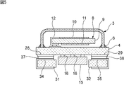
- FIG. 1 is a front cross-sectional view of a quartz crystal vibration device according to a first embodiment of the present invention.
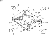
- FIG. 2 is a schematic perspective view showing a relationship between a mounting substrate and an IC chip as a temperature sensitive element used in the first embodiment of the present invention.
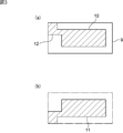
- FIGS. 3A and 3B are a plan view showing the electrode shape on the upper surface of the quartz substrate used in the first embodiment of the present invention, and the plan view of the excitation electrode on the lower surface through the quartz substrate. It is a schematic plan view which shows a shape.
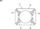
- FIG. 4 is a schematic plan view of a mounting board used in the first embodiment of the present invention.
- FIG. 5 is a front cross-sectional view of a crystal resonator device according to a second embodiment of the present invention.
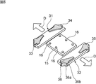
- FIG. 6 is a perspective view showing the relationship between the positional relationship between the first and second mounting substrate members and the IC chip and the heat flow path in the quartz crystal vibrating device according to the second embodiment of the present invention.
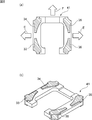
- FIG. 7 is a plan view showing first and second mounting board members used in the third embodiment of the present invention.
- 8A and 8B are a plan view and a perspective view showing a mounting board member used in the fourth embodiment of the present invention.
- FIG. 1 is a front cross-sectional view of a crystal resonator device according to a first embodiment of the present invention.
- the crystal vibration device 1 has a mounting substrate 2.
- the mounting substrate 2 has an upper surface 2a and a lower surface 2b.
- the lower surface 2b of the mounting substrate 2 is a surface on the side where the crystal vibration device 1 is mounted on a circuit substrate or the like.
- the mounting substrate 2 is made of appropriate ceramics such as alumina or synthetic resin.
- the crystal resonator element 3 is mounted above the mounting substrate 2.
- the crystal resonator element 3 includes a package substrate 4 as a first package material and a cap 5 as a second package material.
- a cap 5 having an opening opened downward is bonded to the package substrate 4 by a bonding material 6.
- a crystal resonator 8 is disposed in the hollow space 7.
- the crystal resonator 8 has a crystal substrate 9.
- a first excitation electrode 10 is provided on the upper surface of the quartz substrate 9.
- a second excitation electrode 11 is provided on the lower surface of the quartz substrate 9.
- 3A and 3B show the planar shapes of the first and second excitation electrodes 10 and 11.
- the first excitation electrode 10 and the second excitation electrode 11 are opposed to each other through the quartz substrate 9.
- the extraction electrode 12 is connected to the first excitation electrode 10.
- the extraction electrode 12 reaches the lower surface through the side surface of the crystal substrate 9.
- an electrode land 13 is provided on the upper surface of the package substrate 4.
- the lead electrode 12 is bonded to the electrode land 13 via the conductive bonding material 14.
- the second excitation electrode 11 is also bonded to an electrode land (not shown) with a conductive bonding material.
- the crystal unit 8 is supported by a cantilever beam.
- the first and second excitation electrodes 10, 11, the extraction electrode 12, and the electrode land 13 are made of an appropriate metal or alloy.
- the conductive bonding material 14 is made of an appropriate conductive bonding material such as a conductive adhesive or a metal brazing material.
- the package substrate 4 is made of insulating ceramics such as alumina or other appropriate insulating material.
- the cap 5 is made of metal, but may be made of a material other than metal.
- the bonding material 6 is made of an appropriate adhesive or solder.
- An IC chip 15 having a built-in temperature sensor is fixed to the lower surface of the package substrate 4.
- the IC chip 15 has a plurality of bumps 16 on the upper surface.
- the bumps 16 are bonded to electrodes (not shown) on the lower surface of the package substrate 4.
- the mounting substrate 2 has an opening 2c in the center as shown in FIG.
- the IC chip 15 is located in the opening 2c. Therefore, it is possible to reduce the thickness of the crystal vibration device 1.
- the IC chip 15 has a built-in temperature sensor.
- the IC chip 15 is provided for correcting the frequency characteristics of the crystal resonator 8 in accordance with the ambient temperature change. Accordingly, it is desirable that the temperature difference between the temperature around the IC chip 15 and the crystal resonator 8 sealed in the hollow space 7 and the difference in temperature change are small.
- the air permeability around the IC chip 15 is enhanced by arranging the IC chip 15 in the opening 2c.
- a gap described below is further provided on the side of the IC chip 15. Therefore, a heat flow path is ensured. This will be described more specifically with reference to FIGS.
- FIG. 2 is a schematic perspective view showing the positional relationship between the mounting substrate 2 and the IC chip 15 disposed in the opening 2c.
- FIG. 4 is a plan view showing the mounting substrate 2.
- a plurality of electrode lands 21 to 24 are provided on the mounting substrate 2.
- a broken line A in the plurality of electrode lands 21 to 24 is a portion in which the outer peripheral edge of the package substrate 4 to be mounted is projected downward. Accordingly, the crystal resonator element 3 having the package substrate 4 is mounted above the area surrounded by the broken line.
- electrode lands 22 and 23 are shown among the plurality of electrode lands 21 to 24, electrode lands 22 and 23 are shown. That is, FIG. 1 is a front cross-sectional view of the entire quartz-crystal vibrating device 1 corresponding to a portion along the line BB in FIG.
- the electrode lands 22 and 23 are respectively connected to the side surface portions 22 a and 23 a positioned on the side surface of the mounting substrate 2, and are further terminal portions positioned on the lower surface 2 b of the mounting substrate 2. 22b and 23b.
- the terminal portions 22b and 23b are used as terminals when the crystal resonator device 1 is mounted on another circuit board or the like.
- the electrode lands 21 to 24 are also connected to the terminal portions provided on the lower surface of the mounting substrate 2 in the same manner.
- the electrode lands 21 to 24, the side surface portions 22a and 23a, and the terminal portions 22b and 23b are made of an appropriate metal or alloy.
- the electrode lands 22 and 23 are bonded to bonding electrodes 28 and 29 provided on the lower surface of the package substrate 4 by conductive bonding materials 26 and 27.
- the electrode lands 21 and 24 are also bonded to a bonding electrode provided on the lower surface of the package substrate 4 by a conductive bonding material.
- junction electrodes 28 and 29 are electrically connected to the first and second excitation electrodes 10 and 11 described above by portions not shown.
- the joining electrodes 28 and 29 are made of an appropriate metal or alloy.
- the bonding electrodes 28 and 29 are electrically connected to the IC chip 15 via the bumps 16 through electrodes (not shown) on the lower surface of the package substrate 4 through internal electrodes (not shown) of the package substrate 4.
- first and second excitation electrodes 10 and 11 are finally connected to the IC chip 15 through the conductive bonding material 14 and the electrode land 13 and the internal electrode (not shown) of the package substrate 4. Is electrically connected.
- the conductive bonding materials 26 and 27 are made of a conductive adhesive, a metal brazing material, or the like, like the conductive bonding material 14.
- the feature of this embodiment is that a gap C is provided between the conductive bonding materials 26 and 27 constituting the bonding portion between the mounting substrate 2 and the package substrate 4 around the IC chip 15. . That is, the conductive bonding material is applied to the inner part of the broken line A of the electrode lands 21 to 24 shown in FIG. As shown in FIG. 1, a gap is formed between the electrode lands 22 and 23. Similarly, gaps also exist between the electrode lands 21 and 22, between the electrode lands 23 and 24, and between the electrode lands 24 and 21. Therefore, in the crystal vibration device 1, the gap C is formed on the side of the IC chip 15 at the height position where the mounting substrate 2 is joined to the package substrate 4. Therefore, as shown in FIG. 2, a sufficient heat flow path D is secured on each side.
- the crystal vibration device 1 when the crystal vibration device 1 is mounted on a circuit board or the like, heat from the circuit board side or surrounding circuit elements may be transmitted from the terminal portions 22b and 23b. In such a case, heat is transmitted to the electrode lands 22 and 23, but since the heat flow path D is provided, the heat hardly accumulates around the IC chip 15. Therefore, the temperature rise of the IC chip 15 is suppressed. Therefore, the temperature difference and temperature change difference between the IC chip 15 and the crystal resonator 8 sealed in the hollow space 7 can be reduced. Therefore, the frequency characteristic of the crystal resonator 8 can be accurately corrected by the temperature detected by the temperature sensor built in the IC chip 15.
- FIG. 5 is a front cross-sectional view of a crystal resonator device according to a second embodiment of the present invention.
- the second embodiment differs from the first embodiment in that first and second mounting board members 31 and 32 are used as mounting boards instead of the mounting board 2. Therefore, the description of the first embodiment is incorporated by giving the same reference numerals to other parts.
- FIG. 6 is a perspective view showing the positional relationship between the first and second mounting substrate members 31 and 32 and the IC chip 15.
- the first mounting board member 31 has a strip shape. In other words, it has an elongated rectangular planar shape.
- the first and second mounting substrate members 31 and 32 can be formed of an appropriate insulating material such as alumina.
- electrode lands 33 and 34 are provided on the upper surface of the first mounting board member 31 so as to be separated from each other in the length direction of the first mounting board member 31. Electrode lands 35 and 36 are also provided on the upper surface of the second mounting board member 32 so as to be separated in the longitudinal direction.
- the electrode land 36 has a side surface portion 36a and a terminal portion 36b. The side part 36a and the terminal part 36b are provided similarly to the side part 22a and the terminal part 22b in the first embodiment. Similarly, the other electrode lands 33, 34, and 35 have terminal portions on their side surfaces.
- the electrode lands 34 and 35 are bonded to the bonding electrodes 28 and 29 by the conductive bonding materials 37 and 38.
- the electrode lands 33 and 36 are also bonded to a bonding electrode provided on the lower surface of the package substrate 4 by a conductive bonding material. These conductive bonding materials are applied to the upper surfaces of the electrode lands 33 to 36 shown in FIG.
- a gap is provided between the adjacent conductive bonding materials 37 and 38 as between the conductive bonding materials 37 and 38. That is, not only the gap between the first mounting board member 31 and the second mounting board member 32 but also the height position at which the first and second mounting board members 31 and 32 are joined to the package board 4.
- a gap between the conductive bonding materials is generated between the electrode land 33 and the electrode land 34 and between the electrode land 35 and the electrode land 36 in FIG. Therefore, the heat flow path indicated by arrows D and D in FIG. 6 is formed.
- the second embodiment similarly to the first embodiment, even when heat is transmitted when the crystal vibration device is mounted on a circuit board or the like, it is difficult for heat to be accumulated around the IC chip 15. . Therefore, the temperature rise of the IC chip 15 can be suppressed. Therefore, the temperature difference between the IC chip 15 and the crystal resonator 8 and the temperature change difference can be reduced.
- FIG. 7 is a plan view for explaining a mounting board member used in the third embodiment of the present invention.
- the strip-shaped first and second mounting substrate members 31 and 32 are used.
- the first and second mounting substrate members are strip-shaped mounting substrate member main bodies 31a and 32a, and the opposite mounting substrates from both ends of the mounting substrate member main bodies 31a and 32a. You may have the 1st, 2nd extension part 31b, 31c, 32b, 32c extended toward the member side.
- FIG. 8A and FIG. 8B are a plan view and a perspective view showing a mounting board member used in the fourth embodiment.
- the mounting board member 41 shown in FIGS. 8A and 8B has a part of the frame-like body cut out in plan view, and the inner part and the outer part surrounded by the frame shape communicate with each other. Has a shape.
- the mounting board member 41 has a shape in which at least a part of one side of the rectangular frame shape is cut out.
- the planar shape of the frame shape is not limited to a rectangular shape, and may be a polygonal frame shape other than a circle or a rectangle.
- the first package material is a package substrate and the second package material is a cap, but the first and second package materials are not limited to this.
- a crystal resonator is mounted on the inner bottom surface of a first package material having an opening opened upward, and the upper opening of the first package material is sealed with a lid as a second package material. There may be.
- an IC chip incorporating a temperature sensor is shown as the temperature sensitive element.
- other temperature sensitive elements such as a thermistor may be used.
- mounting board member body 32a mounting board member bodies 31b, 31c, 32b, 32c ... first and second extension parts 33 to 36 ... electrode land 36a ... side face part 36b ... terminal parts 37 and 38 ... conductive bonding material 41 ... mounting board member
Landscapes
- Physics & Mathematics (AREA)
- Acoustics & Sound (AREA)
- Oscillators With Electromechanical Resonators (AREA)
- Piezo-Electric Or Mechanical Vibrators, Or Delay Or Filter Circuits (AREA)
Abstract
温度センサ内蔵ICのような感温性素子の温度変化が生じ難い、水晶振動装置を提供する。 第1のパッケージ材としてのパッケージ基板4上に水晶振動子8が搭載されており、パッケージ基板4が導電性接合材26,27により実装基板2に接合されており、パッケージ基板4と実装基板2との間において、上記導電性接合材26と導電性接合材27により接合されている部分以外が隙間Cとされている、水晶振動装置1。
Description
本発明は、水晶振動子がパッケージ材上に実装されており、該パッケージ材の下面に感温性素子が実装されている、水晶振動装置に関する。
従来、水晶振動装置が発振器等に広く用いられている。例えば、下記の特許文献1には、パッケージ基板上に水晶振動素子を搭載してなる水晶振動装置が開示されている。ここでは、パッケージ基板の下面に、ICチップが固定されている。そして、パッケージ基板の下面において、ICチップを囲む第2の基板が積層されている。この第2の基板は、矩形枠状から一辺を除いた平面形状を有する。
他方、下記の特許文献2に記載の水晶振動装置では、パッケージ基板上に、水晶振動素子が搭載されている。そして、パッケージ基板の下面には、第1の脚部と、第2の脚部とが、間隔を隔てて設けられている。この第1の脚部と第2の脚部との間において、パッケージ基板の下面に電子部品素子が固定されている。
下記の特許文献3では、水晶振動素子が収納されているパッケージの下面に、電子部品チップが固定されている。この電子部品チップの外側には、パッケージ基板の下面に接合されている金属バンプが設けられている。
下記の特許文献4には、水晶振動子が収納されているパッケージと、ICチップが搭載されている実装基板とを、バンプを介して接合してなる構造が開示されている。
特許文献1~3では、ICチップなどの電子部品素子を囲むように設けられた基板や脚部がICチップなどの電子部品の周囲の一部において存在しない。しかしながら、パッケージ基板や周辺の回路素子から熱がパッケージ基板に伝搬してきた場合、上記ICチップなどの電子部品素子の温度が上昇しやすかった。温度センサを内蔵しているICチップが水晶振動素子と組み合わされている構造では、ICチップの温度が上昇した場合、内蔵している温度センサによって周波数補正が行われる。従って、ICチップの周囲の温度が水晶振動子の周囲よりも先に変動すると、周波数ズレが生じるという問題があった。
本発明の目的は、温度センサ内蔵ICのような感温性素子の温度変化が生じ難い、水晶振動装置を提供することにある。
本発明に係る水晶振動装置は、下面を有する第1のパッケージ材と、前記第1のパッケージ材に搭載された水晶振動子と、前記第1のパッケージ材の下面に実装された感温性素子と、前記第1のパッケージ材の下面に接合されており、前記感温性素子の周囲の少なくとも一部に位置している実装基板とを備え、前記実装基板が前記第1のパッケージ材の下面に複数の導電性接合材により接合されており、前記第1のパッケージ材の下面と前記実装基板との間において、前記導電性接合材により接合されている部分以外が隙間とされている。
本発明に係る水晶振動装置のある特定の局面では、前記実装基板の上面に複数の電極ランドが設けられており、前記複数の導電性接合材が、前記複数の電極ランドと、前記第1のパッケージ材とを接合している。
本発明に係る水晶振動装置の他の特定の局面では、前記実装基板が、開口部を有し、該開口部内に前記感温性素子が位置している。
本発明に係る水晶振動装置のさらに他の特定の局面では、前記実装基板が、第1の実装基板部材と、該第1の実装基板部材と隔てられた第2の実装基板部材とを有し、前記第1の実装基板部材と、前記第2の実装基板部材との間に前記感温性素子が位置している。
本発明に係る水晶振動装置のさらに別の特定の局面では、前記第1,第2の実装基板部材が、ストリップ状の形状を有する。
本発明に係る水晶振動装置のさらに他の特定の局面では、前記第1,第2の実装基板部材が、ストリップ状の実装基板部材本体と、前記実装基板部材本体の両端から相手側の実装基板部材側に向かって延びる第1,第2の延長部とを有する。
本発明に係る水晶振動装置のさらに他の特定の局面では、前記実装基板が、平面視において、枠状体の一部が切り欠かれており、前記枠状体で囲まれた内側部分と外側部分とが連通されている形状を有する。
本発明に係る水晶振動装置の別の特定の局面では、前記枠状体が矩形枠状の形状を有し、矩形枠状のうちの一辺の少なくとも一部が切り欠かれている。
本発明に係る水晶振動装置のさらに他の特定の局面では、前記第1のパッケージ材上に取付けられており、前記第1のパッケージ材とともに、前記水晶振動子を収納している封止空間を形成する第2のパッケージ材がさらに備えられている。
本発明に係る水晶振動装置の別の特定の局面では、前記第1のパッケージ材が、パッケージ基板である。
本発明に係る水晶振動装置によれば、実装基板から熱が伝わってきたとしても、実装基板と素子基板との間において、熱流路が形成されるため、感温性素子の温度上昇を抑制することができる。
以下、図面を参照しつつ、本発明の具体的な実施形態を説明することにより、本発明を明らかにする。
図1は、本発明の第1の実施形態に係る水晶振動装置の正面断面図である。
水晶振動装置1は、実装基板2を有する。実装基板2は、上面2aと下面2bとを有する。実装基板2の下面2bが、水晶振動装置1を回路基板などに実装する側の面となる。
実装基板2は、アルミナなどの適宜のセラミックス、あるいは合成樹脂からなる。
実装基板2の上方に水晶振動素子3が搭載されている。水晶振動素子3は、第1のパッケージ材としてのパッケージ基板4と、第2のパッケージ材としてのキャップ5とを有する。パッケージ基板4に、下方に開いた開口を有するキャップ5が接合材6により接合されている。それによって、封止された中空空間7が形成されている。中空空間7内に水晶振動子8が配置されている。水晶振動子8は、水晶基板9を有する。水晶基板9の上面には、第1の励振電極10が設けられている。水晶基板9の下面には、第2の励振電極11が設けられている。
図3(a)及び図3(b)に、第1,第2の励振電極10,11の平面形状を示す。
第1の励振電極10と、第2の励振電極11とは、水晶基板9を介して対向している。図3(a)に示すように、引き出し電極12が第1の励振電極10に連ねられている。引き出し電極12は、図1に示すように、水晶基板9の側面を経て下面に至っている。
図1に示すように、パッケージ基板4の上面には、電極ランド13が設けられている。この電極ランド13に、導電性接合材14を介して引き出し電極12が接合されている。第2の励振電極11についても、図示しない電極ランドに導電性接合材により接合されている。それによって、水晶振動子8は、片持ち梁で支持されている。
上記第1,第2の励振電極10,11、引き出し電極12、及び電極ランド13は、適宜の金属もしくは合金からなる。導電性接合材14は、導電性接着材や金属のろう材などの適宜の導電性接合材からなる。
また、上記パッケージ基板4は、アルミナなどの絶縁性セラミックス、あるいは他の適宜の絶縁性材料からなる。キャップ5は、金属からなるが、金属以外の他の材料からなるものであってもよい。接合材6は、適宜の接着材もしくははんだからなる。
上記パッケージ基板4の下面には、温度センサが内蔵されているICチップ15が固定されている。ICチップ15は、複数のバンプ16を上面に有する。このバンプ16が、パッケージ基板4の下面の電極(図示せず)に接合されている。
実装基板2は、図2に示すように、中央に開口部2cを有する。この開口部2c内にICチップ15が位置している。従って、水晶振動装置1の薄型化を図ることが可能とされている。
上記ICチップ15は、温度センサを内蔵している。ICチップ15は、周囲の温度変化に応じて水晶振動子8の周波数特性に補正をかけるために設けられている。従って、ICチップ15の周囲の温度と、中空空間7内に封止されている水晶振動子8との温度差及び温度変化の度合いの差が小さいことが望ましい。
従って、上記開口部2c内にICチップ15を配置することにより、ICチップ15の周囲における通気性が高められている。
もっとも、本実施形態では、さらに、ICチップ15の側方に、以下に述べる隙間が設けられている。そのため、熱流路が確保される。これを、図1及び図2を参照してより具体的に説明する。
図2は、実装基板2と、開口部2cに配置されているICチップ15との位置関係を示す略図的斜視図である。図4は、実装基板2を示す平面図である。
実装基板2上には、複数の電極ランド21~24が設けられている。複数の電極ランド21~24内の破線Aは、実装されるパッケージ基板4の外周縁を下方に投影した部分である。従って、この破線で囲まれた領域の上方にパッケージ基板4を有する水晶振動素子3が搭載される。図1では、上記複数の電極ランド21~24のうち、電極ランド22,23が図示されている。すなわち、図1は、図2のB-B線に沿う部分に相当する水晶振動装置1全体の正面断面図である。
図1に示すように、電極ランド22,23は、それぞれ、実装基板2の側面に位置している側面部22a,23aに連なっており、さらに実装基板2の下面2bに位置している端子部22b,23bに連なっている。この端子部22b,23bが、水晶振動装置1を他の回路基板等に実装する際の端子として用いられる。
特に図示はしないが、電極ランド21~24も、同様に、実装基板2の下面に設けられた端子部に連ねられている。
上記電極ランド21~24及び側面部22a,23a並びに端子部22b,23bは、適宜の金属もしくは合金からなる。
また、図1に示すように、上記電極ランド22,23は、導電性接合材26,27により、パッケージ基板4の下面に設けられた接合電極28,29に接合されている。特に図示はしないが、電極ランド22,23と同様に、電極ランド21,24も導電性接合材により、パッケージ基板4の下面に設けられた接合電極に接合されている。
接合電極28,29は、前述した第1,第2の励振電極10,11に図示されていない部分により電気的に接続されている。上記接合電極28,29は、適宜の金属もしくは合金からなる。
接合電極28,29は、パッケージ基板4の図示されていない内部の電極などを通じて、パッケージ基板4の下面の電極(図示せず)を通り、バンプ16を介してICチップ15に電気的に接続される。
同様に、前述した第1,第2の励振電極10,11も導電性接合材14及び電極ランド13を介して、パッケージ基板4の内部電極(図示せず)などを通じて、最終的にICチップ15に電気的に接続される。
導電性接合材26,27は、導電性接合材14と同様に、導電性接着材や金属のろう材などからなる。
本実施形態の特徴は、ICチップ15の周囲において、上記実装基板2とパッケージ基板4との接合部分を構成している導電性接合材26,27間に隙間Cが設けられていることにある。すなわち、導電性接合材は、図2に示す電極ランド21~24の上記破線Aの内側部分に適用される。図1に示すように、電極ランド22,23間に隙間が形成される。電極ランド21,22間、電極ランド23,24間及び電極ランド24,21間にも同様に隙間が存在することとなる。従って、水晶振動装置1では、実装基板2がパッケージ基板4と接合されている高さ位置において、上記隙間CがICチップ15の側方に形成される。よって、図2に示すように、十分な熱流路Dが各辺において確保される。
他方、水晶振動装置1を回路基板などに実装した場合、回路基板側から、あるいは周囲の回路素子からの熱が、端子部22b,23bから伝わることがある。このような場合、熱が電極ランド22,23に伝わるが、上記熱流路Dが設けられているため、ICチップ15の周囲に熱がこもり難い。従って、ICチップ15の温度上昇が抑制される。よってICチップ15と、中空空間7に封止されている水晶振動子8との温度の差や温度変化の差を小さくすることができる。そのため、ICチップ15に内蔵されている温度センサで検出した温度によって、水晶振動子8の周波数特性を的確に補正することができる。
図5は、本発明の第2の実施形態に係る水晶振動装置の正面断面図である。第2の実施形態が第1の実施形態と異なるところは、実装基板2に代えて、実装基板として、第1,第2の実装基板部材31,32が用いられていることにある。従って、他の部分については、同一の参照番号を付することにより、第1の実施形態の説明を援用することとする。
第2の実施形態では、パッケージ基板4の下面に、第1,第2の実装基板部材31,32が接合されている。第1,第2の実装基板部材31,32と、ICチップ15との位置関係を、図6に斜視図で示す。
図5及び図6に示すように、第1の実装基板部材31は、ストリップ状の形状を有する。言い換えれば、細長い矩形の平面形状を有する。第1,第2の実装基板部材31,32は、アルミナなどの適宜の絶縁性材料により形成され得る。
図6に示すように、第1の実装基板部材31の上面には、電極ランド33,34が第1の実装基板部材31の長さ方向において隔てられて設けられている。第2の実装基板部材32の上面にも、電極ランド35,36が、長手方向において隔てられて設けられている。電極ランド36は、側面部36a及び端子部36bを有する。側面部36a及び端子部36bは、第1の実施形態における側面部22a及び端子部22bと同様に設けられている。他の電極ランド33,34,35も同様に側面部が端子部を有する。
本実施形態では、図5に示すように、電極ランド34,35が、導電性接合材37,38により、接合電極28,29に接合されている。電極ランド33,36も導電性接合材によりパッケージ基板4の下面に設けられた接合電極に接合されている。これらの導電性接合材は、図6に示した電極ランド33~36の上面に適用される。
従って、導電性接合材37,38間のように、隣り合う導電性接合材37,38間に隙間が設けられる。すなわち、第1の実装基板部材31と第2の実装基板部材32との間の隙間だけでなく、第1,第2の実装基板部材31,32がパッケージ基板4と接合されている高さ位置において、図6の電極ランド33と電極ランド34との間、及び電極ランド35と電極ランド36との間において、導電性接合材間の隙間が生じることとなる。よって、図6の矢印D,Dで示す熱流路が形成されることとなる。
よって、第2の実施形態においても、第1の実施形態と同様に、回路基板などに水晶振動装置が実装された場合に熱が伝わってきたとしても、ICチップ15の周囲に熱がこもり難い。従って、ICチップ15の温度上昇を抑制することができる。よって、ICチップ15及び水晶振動子8の温度の差及び温度変化の差を小さくすることができる。
図7は、本発明の第3の実施形態で用いられる実装基板部材を説明するための平面図である。第2の実施形態では、ストリップ状の第1,第2の実装基板部材31,32を用いた。これに対して、図7に示すように、第1,第2の実装基板部材が、ストリップ状の実装基板部材本体31a,32aと、実装基板部材本体31a,32aの両端から相手側の実装基板部材側に向かって延びる第1,第2の延長部31b,31c,32b,32cを有していてもよい。
この場合においても、電極ランド33,34間及び電極ランド35,36間において、隣り合う導電性接合材間に熱流路を形成するための隙間が形成されることとなる。従って、第2の実施形態と同様の効果が得られる。
さらに、図8(a)及び図8(b)は、第4の実施形態で用いられる実装基板部材を示す平面図及び斜視図である。図8(a),図8(b)に示す実装基板部材41は、平面視において、枠状体の一部を切り欠き、枠状で囲まれた内側部分と外側部分とが連通されている形状を有する。言い換えれば、実装基板部材41は、矩形枠状の形状の一辺の内の少なくとも一部を切り欠いた形状とされている。もっとも、この枠状の平面形状は矩形形状に限らず、円形や四角形以外の多角形の枠状体であってもよい。
実装基板部材41を用いた場合においても、電極ランド33~36が第2の実施形態と同様に構成されているため、矢印E,Eで示す方向に熱が移動し得る熱流路が形成される。さらに、本実施形態では、矢印Fで示す方向においても、隣り合う導電性接合材間に隙間が形成され、熱流路が形成される。従って、ICチップの周囲により一層熱がこもり難い。
第1及び第2の実施形態では、第1のパッケージ材がパッケージ基板であり、第2のパッケージ材がキャップであったが、第1,第2のパッケージ材はこれに限定されない。例えば、上方に開いた開口を有する第1のパッケージ材の内底面上に水晶振動子を実装し、該第1のパッケージ材の上方開口を第2のパッケージ材としての蓋を封止した構造であってもよい。
また、上記第1,第2の実施形態では、感温性素子として、温度センサを内蔵したICチップを示したが、サーミスタなどの他の感温性素子であってもよい。
1…水晶振動装置
2…実装基板
2a…上面
2b…下面
2c…開口部
3…水晶振動素子
4…パッケージ基板
5…キャップ
6…接合材
7…中空空間
8…水晶振動子
9…水晶基板
10…第1の励振電極
11…第2の励振電極
12…引き出し電極
13…電極ランド
14…導電性接合材
15…ICチップ
16…バンプ
21~24…電極ランド
22a,23a…側面部
22b,23b…端子部
26,27…導電性接合材
28,29…接合電極
31…第1の実装基板部材
32…第2の実装基板部材
31a…実装基板部材本体
32a…実装基板部材本体
31b,31c,32b,32c…第1,第2の延長部
33~36…電極ランド
36a…側面部
36b…端子部
37,38…導電性接合材
41…実装基板部材
2…実装基板
2a…上面
2b…下面
2c…開口部
3…水晶振動素子
4…パッケージ基板
5…キャップ
6…接合材
7…中空空間
8…水晶振動子
9…水晶基板
10…第1の励振電極
11…第2の励振電極
12…引き出し電極
13…電極ランド
14…導電性接合材
15…ICチップ
16…バンプ
21~24…電極ランド
22a,23a…側面部
22b,23b…端子部
26,27…導電性接合材
28,29…接合電極
31…第1の実装基板部材
32…第2の実装基板部材
31a…実装基板部材本体
32a…実装基板部材本体
31b,31c,32b,32c…第1,第2の延長部
33~36…電極ランド
36a…側面部
36b…端子部
37,38…導電性接合材
41…実装基板部材
Claims (10)
- 下面を有する第1のパッケージ材と、
前記第1のパッケージ材に搭載された水晶振動子と、
前記第1のパッケージ材の下面に実装された感温性素子と、
前記第1のパッケージ材の下面に接合されており、前記感温性素子の周囲の少なくとも一部に位置している実装基板とを備え、
前記実装基板が前記第1のパッケージ材の下面に複数の導電性接合材により接合されており、前記第1のパッケージ材の下面と前記実装基板との間において、前記導電性接合材により接合されている部分以外が隙間とされている、水晶振動装置。 - 前記実装基板の上面に複数の電極ランドが設けられており、前記複数の導電性接合材が、前記複数の電極ランドと、前記第1のパッケージ材とを接合している、請求項1に記載の水晶振動装置。
- 前記実装基板が、開口部を有し、該開口部内に前記感温性素子が位置している、請求項1または2に記載の水晶振動装置。
- 前記実装基板が、第1の実装基板部材と、該第1の実装基板部材と隔てられた第2の実装基板部材とを有し、前記第1の実装基板部材と、前記第2の実装基板部材との間に前記感温性素子が位置している、請求項1または2に記載の水晶振動装置。
- 前記第1,第2の実装基板部材が、ストリップ状の形状を有する、請求項4に記載の水晶振動装置。
- 前記第1,第2の実装基板部材が、ストリップ状の実装基板部材本体と、前記実装基板部材本体の両端から相手側の実装基板部材側に向かって延びる第1,第2の延長部とを有する、請求項4または5に記載の水晶振動装置。
- 前記実装基板が、平面視において、枠状体の一部が切り欠かれており、前記枠状体で囲まれた内側部分と外側部分とが連通されている形状を有する、請求項1または2に記載の水晶振動装置。
- 前記枠状体が矩形枠状の形状を有し、矩形枠状のうちの一辺の少なくとも一部が切り欠かれている、請求項7に記載の水晶振動装置。
- 前記第1のパッケージ材上に取付けられており、前記第1のパッケージ材とともに、前記水晶振動子を収納している封止空間を形成する第2のパッケージ材をさらに備える、請求項1~8のいずれか1項に記載の水晶振動装置。
- 前記第1のパッケージ材が、パッケージ基板である、請求項1~9のいずれか1項に記載の水晶振動装置。
Priority Applications (3)
| Application Number | Priority Date | Filing Date | Title |
|---|---|---|---|
| CN201580010515.2A CN106031032B (zh) | 2014-05-07 | 2015-01-20 | 水晶振荡装置 |
| JP2016517820A JP6041070B2 (ja) | 2014-05-07 | 2015-01-20 | 水晶振動装置 |
| US15/333,619 US10122366B2 (en) | 2014-05-07 | 2016-10-25 | Crystal oscillation device |
Applications Claiming Priority (2)
| Application Number | Priority Date | Filing Date | Title |
|---|---|---|---|
| JP2014-096022 | 2014-05-07 | ||
| JP2014096022 | 2014-05-07 |
Related Child Applications (1)
| Application Number | Title | Priority Date | Filing Date |
|---|---|---|---|
| US15/333,619 Continuation US10122366B2 (en) | 2014-05-07 | 2016-10-25 | Crystal oscillation device |
Publications (1)
| Publication Number | Publication Date |
|---|---|
| WO2015170484A1 true WO2015170484A1 (ja) | 2015-11-12 |
Family
ID=54392339
Family Applications (1)
| Application Number | Title | Priority Date | Filing Date |
|---|---|---|---|
| PCT/JP2015/051346 Ceased WO2015170484A1 (ja) | 2014-05-07 | 2015-01-20 | 水晶振動装置 |
Country Status (5)
| Country | Link |
|---|---|
| US (1) | US10122366B2 (ja) |
| JP (1) | JP6041070B2 (ja) |
| CN (1) | CN106031032B (ja) |
| TW (1) | TWI581566B (ja) |
| WO (1) | WO2015170484A1 (ja) |
Cited By (3)
| Publication number | Priority date | Publication date | Assignee | Title |
|---|---|---|---|---|
| JP2017130862A (ja) * | 2016-01-22 | 2017-07-27 | 株式会社大真空 | 圧電発振器 |
| JP2020043433A (ja) * | 2018-09-07 | 2020-03-19 | 京セラ株式会社 | 水晶デバイス |
| JP2020115688A (ja) * | 2020-04-20 | 2020-07-30 | 株式会社大真空 | 圧電発振器 |
Families Citing this family (2)
| Publication number | Priority date | Publication date | Assignee | Title |
|---|---|---|---|---|
| CN106411283A (zh) * | 2016-10-18 | 2017-02-15 | 应达利电子股份有限公司 | 一种石英晶体振荡器及其制备方法 |
| CN111883516A (zh) * | 2020-07-24 | 2020-11-03 | 青岛歌尔智能传感器有限公司 | 集成模组的封装结构及其封装方法、以及电子设备 |
Citations (5)
| Publication number | Priority date | Publication date | Assignee | Title |
|---|---|---|---|---|
| JP2004297211A (ja) * | 2003-03-25 | 2004-10-21 | Kyocera Corp | 表面実装型圧電発振器 |
| JP2005159575A (ja) * | 2003-11-21 | 2005-06-16 | Toyo Commun Equip Co Ltd | 表面実装型圧電発振器 |
| JP2008141413A (ja) * | 2006-11-30 | 2008-06-19 | Kyocera Kinseki Corp | 圧電発振器及びその製造方法 |
| JP2009016949A (ja) * | 2007-06-29 | 2009-01-22 | Kyocera Kinseki Corp | 圧電発振器 |
| JP2012175499A (ja) * | 2011-02-23 | 2012-09-10 | Seiko Epson Corp | 圧電振動子、圧電発振器、及び電子機器 |
Family Cites Families (17)
| Publication number | Priority date | Publication date | Assignee | Title |
|---|---|---|---|---|
| US6229249B1 (en) * | 1998-08-31 | 2001-05-08 | Kyocera Corporation | Surface-mount type crystal oscillator |
| JP2003318653A (ja) | 2002-04-24 | 2003-11-07 | Daishinku Corp | 圧電振動デバイス |
| JP2004032456A (ja) | 2002-06-27 | 2004-01-29 | Nippon Dempa Kogyo Co Ltd | 表面実装用水晶発振器 |
| US20050040905A1 (en) * | 2003-05-29 | 2005-02-24 | Kyocera Corporation | Temperature-compensated crystal oscillator |
| JP4113465B2 (ja) | 2003-06-27 | 2008-07-09 | 京セラ株式会社 | 温度補償型水晶発振器の製造方法 |
| JP4354347B2 (ja) * | 2004-06-29 | 2009-10-28 | 日本電波工業株式会社 | 水晶発振器 |
| JP4713215B2 (ja) * | 2005-04-28 | 2011-06-29 | 日本電波工業株式会社 | 表面実装水晶発振器の実装方法 |
| JP2010087726A (ja) | 2008-09-30 | 2010-04-15 | Nippon Dempa Kogyo Co Ltd | 表面実装用の水晶発振器 |
| JP5220584B2 (ja) * | 2008-12-27 | 2013-06-26 | 京セラクリスタルデバイス株式会社 | 圧電発振器及びその製造方法 |
| US9252782B2 (en) * | 2011-02-14 | 2016-02-02 | Qualcomm Incorporated | Wireless chipset with a non-temperature compensated crystal reference |
| TW201334404A (zh) * | 2012-02-08 | 2013-08-16 | Pse Technology Corp | 頻率產生裝置之封裝結構 |
| JP2013207686A (ja) * | 2012-03-29 | 2013-10-07 | Nippon Dempa Kogyo Co Ltd | 水晶発振器 |
| JP6123979B2 (ja) * | 2012-05-23 | 2017-05-10 | セイコーエプソン株式会社 | 発振装置及び電子機器 |
| TWM458034U (zh) * | 2013-03-27 | 2013-07-21 | Harmony Electronics Corp | 具熱敏電阻元件之石英振盪器封裝結構 |
| JP6183156B2 (ja) * | 2013-10-30 | 2017-08-23 | セイコーエプソン株式会社 | パッケージ、振動デバイス、発振器、電子機器及び移動体 |
| US10103709B2 (en) * | 2013-11-05 | 2018-10-16 | Kyocera Corporation | Crystal unit |
| US9287882B2 (en) * | 2013-11-07 | 2016-03-15 | Kyocera Crystal Device Corporation | Temperature compensated crystal oscillator |
-
2015
- 2015-01-20 JP JP2016517820A patent/JP6041070B2/ja active Active
- 2015-01-20 CN CN201580010515.2A patent/CN106031032B/zh active Active
- 2015-01-20 WO PCT/JP2015/051346 patent/WO2015170484A1/ja not_active Ceased
- 2015-04-16 TW TW104112202A patent/TWI581566B/zh active
-
2016
- 2016-10-25 US US15/333,619 patent/US10122366B2/en active Active
Patent Citations (5)
| Publication number | Priority date | Publication date | Assignee | Title |
|---|---|---|---|---|
| JP2004297211A (ja) * | 2003-03-25 | 2004-10-21 | Kyocera Corp | 表面実装型圧電発振器 |
| JP2005159575A (ja) * | 2003-11-21 | 2005-06-16 | Toyo Commun Equip Co Ltd | 表面実装型圧電発振器 |
| JP2008141413A (ja) * | 2006-11-30 | 2008-06-19 | Kyocera Kinseki Corp | 圧電発振器及びその製造方法 |
| JP2009016949A (ja) * | 2007-06-29 | 2009-01-22 | Kyocera Kinseki Corp | 圧電発振器 |
| JP2012175499A (ja) * | 2011-02-23 | 2012-09-10 | Seiko Epson Corp | 圧電振動子、圧電発振器、及び電子機器 |
Cited By (3)
| Publication number | Priority date | Publication date | Assignee | Title |
|---|---|---|---|---|
| JP2017130862A (ja) * | 2016-01-22 | 2017-07-27 | 株式会社大真空 | 圧電発振器 |
| JP2020043433A (ja) * | 2018-09-07 | 2020-03-19 | 京セラ株式会社 | 水晶デバイス |
| JP2020115688A (ja) * | 2020-04-20 | 2020-07-30 | 株式会社大真空 | 圧電発振器 |
Also Published As
| Publication number | Publication date |
|---|---|
| TWI581566B (zh) | 2017-05-01 |
| US10122366B2 (en) | 2018-11-06 |
| TW201543813A (zh) | 2015-11-16 |
| CN106031032B (zh) | 2018-09-25 |
| CN106031032A (zh) | 2016-10-12 |
| JP6041070B2 (ja) | 2016-12-07 |
| JPWO2015170484A1 (ja) | 2017-04-20 |
| US20170041007A1 (en) | 2017-02-09 |
Similar Documents
| Publication | Publication Date | Title |
|---|---|---|
| JP6164326B2 (ja) | 圧電振動デバイス | |
| JP5339681B2 (ja) | 表面実装用の水晶振動子 | |
| US8941445B2 (en) | Piezoelectric module | |
| JP5900582B1 (ja) | 圧電振動デバイス | |
| JP6041070B2 (ja) | 水晶振動装置 | |
| JP2013207686A5 (ja) | ||
| JP6460720B2 (ja) | 圧電デバイス及び圧電デバイスの製造方法 | |
| JP6547825B2 (ja) | 圧電振動デバイス | |
| JP6565671B2 (ja) | 圧電デバイス | |
| JP6032384B2 (ja) | 水晶振動装置 | |
| JP2009004900A (ja) | 表面実装用の水晶発振器 | |
| JP5101201B2 (ja) | 圧電発振器 | |
| KR101532134B1 (ko) | 압전 소자 패키지 및 그 제조 방법 | |
| CN111106810B (zh) | 压电器件 | |
| JP5643040B2 (ja) | 圧電発振器 | |
| JP2009105199A (ja) | 電子デバイス | |
| JP6590529B2 (ja) | 圧電デバイス | |
| JP5451266B2 (ja) | 電子デバイス | |
| JP5468327B2 (ja) | 圧電デバイス | |
| WO2015045906A1 (ja) | 水晶発振器 | |
| JP2015226308A (ja) | 水晶発振器 | |
| JP4359933B2 (ja) | 水晶発振器 | |
| JP2016174317A (ja) | 圧電デバイス | |
| JP2014011258A (ja) | 電子部品用パッケージ及び電子部品 | |
| JP2016009985A (ja) | 圧電デバイス |
Legal Events
| Date | Code | Title | Description |
|---|---|---|---|
| 121 | Ep: the epo has been informed by wipo that ep was designated in this application |
Ref document number: 15789463 Country of ref document: EP Kind code of ref document: A1 |
|
| ENP | Entry into the national phase |
Ref document number: 2016517820 Country of ref document: JP Kind code of ref document: A |
|
| NENP | Non-entry into the national phase |
Ref country code: DE |
|
| 122 | Ep: pct application non-entry in european phase |
Ref document number: 15789463 Country of ref document: EP Kind code of ref document: A1 |