WO2015166572A1 - 半導体装置および半導体装置の製造方法 - Google Patents
半導体装置および半導体装置の製造方法 Download PDFInfo
- Publication number
- WO2015166572A1 WO2015166572A1 PCT/JP2014/062095 JP2014062095W WO2015166572A1 WO 2015166572 A1 WO2015166572 A1 WO 2015166572A1 JP 2014062095 W JP2014062095 W JP 2014062095W WO 2015166572 A1 WO2015166572 A1 WO 2015166572A1
- Authority
- WO
- WIPO (PCT)
- Prior art keywords
- metal
- film
- semiconductor device
- oxide film
- gate insulating
- Prior art date
- Legal status (The legal status is an assumption and is not a legal conclusion. Google has not performed a legal analysis and makes no representation as to the accuracy of the status listed.)
- Ceased
Links
Images











Classifications
-
- H—ELECTRICITY
- H10—SEMICONDUCTOR DEVICES; ELECTRIC SOLID-STATE DEVICES NOT OTHERWISE PROVIDED FOR
- H10D—INORGANIC ELECTRIC SEMICONDUCTOR DEVICES
- H10D30/00—Field-effect transistors [FET]
- H10D30/01—Manufacture or treatment
- H10D30/015—Manufacture or treatment of FETs having heterojunction interface channels or heterojunction gate electrodes, e.g. HEMT
-
- H—ELECTRICITY
- H10—SEMICONDUCTOR DEVICES; ELECTRIC SOLID-STATE DEVICES NOT OTHERWISE PROVIDED FOR
- H10D—INORGANIC ELECTRIC SEMICONDUCTOR DEVICES
- H10D30/00—Field-effect transistors [FET]
- H10D30/01—Manufacture or treatment
- H10D30/021—Manufacture or treatment of FETs having insulated gates [IGFET]
-
- H—ELECTRICITY
- H10—SEMICONDUCTOR DEVICES; ELECTRIC SOLID-STATE DEVICES NOT OTHERWISE PROVIDED FOR
- H10D—INORGANIC ELECTRIC SEMICONDUCTOR DEVICES
- H10D30/00—Field-effect transistors [FET]
- H10D30/40—FETs having zero-dimensional [0D], one-dimensional [1D] or two-dimensional [2D] charge carrier gas channels
- H10D30/47—FETs having zero-dimensional [0D], one-dimensional [1D] or two-dimensional [2D] charge carrier gas channels having two-dimensional [2D] charge carrier gas channels, e.g. nanoribbon FETs or high electron mobility transistors [HEMT]
-
- H—ELECTRICITY
- H10—SEMICONDUCTOR DEVICES; ELECTRIC SOLID-STATE DEVICES NOT OTHERWISE PROVIDED FOR
- H10D—INORGANIC ELECTRIC SEMICONDUCTOR DEVICES
- H10D30/00—Field-effect transistors [FET]
- H10D30/40—FETs having zero-dimensional [0D], one-dimensional [1D] or two-dimensional [2D] charge carrier gas channels
- H10D30/47—FETs having zero-dimensional [0D], one-dimensional [1D] or two-dimensional [2D] charge carrier gas channels having two-dimensional [2D] charge carrier gas channels, e.g. nanoribbon FETs or high electron mobility transistors [HEMT]
- H10D30/471—High electron mobility transistors [HEMT] or high hole mobility transistors [HHMT]
- H10D30/475—High electron mobility transistors [HEMT] or high hole mobility transistors [HHMT] having wider bandgap layer formed on top of lower bandgap active layer, e.g. undoped barrier HEMTs such as i-AlGaN/GaN HEMTs
-
- H—ELECTRICITY
- H10—SEMICONDUCTOR DEVICES; ELECTRIC SOLID-STATE DEVICES NOT OTHERWISE PROVIDED FOR
- H10D—INORGANIC ELECTRIC SEMICONDUCTOR DEVICES
- H10D30/00—Field-effect transistors [FET]
- H10D30/40—FETs having zero-dimensional [0D], one-dimensional [1D] or two-dimensional [2D] charge carrier gas channels
- H10D30/47—FETs having zero-dimensional [0D], one-dimensional [1D] or two-dimensional [2D] charge carrier gas channels having two-dimensional [2D] charge carrier gas channels, e.g. nanoribbon FETs or high electron mobility transistors [HEMT]
- H10D30/471—High electron mobility transistors [HEMT] or high hole mobility transistors [HHMT]
- H10D30/476—High electron mobility transistors [HEMT] or high hole mobility transistors [HHMT] having gate trenches interrupting the 2D charge carrier gas channels, e.g. hybrid MOS-HEMTs
-
- H—ELECTRICITY
- H10—SEMICONDUCTOR DEVICES; ELECTRIC SOLID-STATE DEVICES NOT OTHERWISE PROVIDED FOR
- H10D—INORGANIC ELECTRIC SEMICONDUCTOR DEVICES
- H10D30/00—Field-effect transistors [FET]
- H10D30/60—Insulated-gate field-effect transistors [IGFET]
-
- H—ELECTRICITY
- H10—SEMICONDUCTOR DEVICES; ELECTRIC SOLID-STATE DEVICES NOT OTHERWISE PROVIDED FOR
- H10D—INORGANIC ELECTRIC SEMICONDUCTOR DEVICES
- H10D62/00—Semiconductor bodies, or regions thereof, of devices having potential barriers
- H10D62/80—Semiconductor bodies, or regions thereof, of devices having potential barriers characterised by the materials
- H10D62/82—Heterojunctions
- H10D62/824—Heterojunctions comprising only Group III-V materials heterojunctions, e.g. GaN/AlGaN heterojunctions
-
- H—ELECTRICITY
- H10—SEMICONDUCTOR DEVICES; ELECTRIC SOLID-STATE DEVICES NOT OTHERWISE PROVIDED FOR
- H10D—INORGANIC ELECTRIC SEMICONDUCTOR DEVICES
- H10D64/00—Electrodes of devices having potential barriers
- H10D64/20—Electrodes characterised by their shapes, relative sizes or dispositions
- H10D64/27—Electrodes not carrying the current to be rectified, amplified, oscillated or switched, e.g. gates
- H10D64/311—Gate electrodes for field-effect devices
- H10D64/411—Gate electrodes for field-effect devices for FETs
- H10D64/511—Gate electrodes for field-effect devices for FETs for IGFETs
- H10D64/514—Gate electrodes for field-effect devices for FETs for IGFETs characterised by the insulating layers
-
- H—ELECTRICITY
- H10—SEMICONDUCTOR DEVICES; ELECTRIC SOLID-STATE DEVICES NOT OTHERWISE PROVIDED FOR
- H10D—INORGANIC ELECTRIC SEMICONDUCTOR DEVICES
- H10D64/00—Electrodes of devices having potential barriers
- H10D64/60—Electrodes characterised by their materials
- H10D64/66—Electrodes having a conductor capacitively coupled to a semiconductor by an insulator, e.g. MIS electrodes
- H10D64/68—Electrodes having a conductor capacitively coupled to a semiconductor by an insulator, e.g. MIS electrodes characterised by the insulator, e.g. by the gate insulator
- H10D64/681—Electrodes having a conductor capacitively coupled to a semiconductor by an insulator, e.g. MIS electrodes characterised by the insulator, e.g. by the gate insulator having a compositional variation, e.g. multilayered
- H10D64/685—Electrodes having a conductor capacitively coupled to a semiconductor by an insulator, e.g. MIS electrodes characterised by the insulator, e.g. by the gate insulator having a compositional variation, e.g. multilayered being perpendicular to the channel plane
-
- H—ELECTRICITY
- H10—SEMICONDUCTOR DEVICES; ELECTRIC SOLID-STATE DEVICES NOT OTHERWISE PROVIDED FOR
- H10D—INORGANIC ELECTRIC SEMICONDUCTOR DEVICES
- H10D64/00—Electrodes of devices having potential barriers
- H10D64/60—Electrodes characterised by their materials
- H10D64/66—Electrodes having a conductor capacitively coupled to a semiconductor by an insulator, e.g. MIS electrodes
- H10D64/68—Electrodes having a conductor capacitively coupled to a semiconductor by an insulator, e.g. MIS electrodes characterised by the insulator, e.g. by the gate insulator
- H10D64/691—Electrodes having a conductor capacitively coupled to a semiconductor by an insulator, e.g. MIS electrodes characterised by the insulator, e.g. by the gate insulator comprising metallic compounds, e.g. metal oxides or metal silicates
-
- H—ELECTRICITY
- H10—SEMICONDUCTOR DEVICES; ELECTRIC SOLID-STATE DEVICES NOT OTHERWISE PROVIDED FOR
- H10P—GENERIC PROCESSES OR APPARATUS FOR THE MANUFACTURE OR TREATMENT OF DEVICES COVERED BY CLASS H10
- H10P14/00—Formation of materials, e.g. in the shape of layers or pillars
- H10P14/60—Formation of materials, e.g. in the shape of layers or pillars of insulating materials
- H10P14/63—Formation of materials, e.g. in the shape of layers or pillars of insulating materials characterised by the formation processes
- H10P14/6326—Deposition processes
- H10P14/6328—Deposition from the gas or vapour phase
- H10P14/6334—Deposition from the gas or vapour phase using decomposition or reaction of gaseous or vapour phase compounds, i.e. chemical vapour deposition
- H10P14/6339—Deposition from the gas or vapour phase using decomposition or reaction of gaseous or vapour phase compounds, i.e. chemical vapour deposition deposition by cyclic CVD, e.g. ALD, ALE or pulsed CVD
-
- H—ELECTRICITY
- H10—SEMICONDUCTOR DEVICES; ELECTRIC SOLID-STATE DEVICES NOT OTHERWISE PROVIDED FOR
- H10P—GENERIC PROCESSES OR APPARATUS FOR THE MANUFACTURE OR TREATMENT OF DEVICES COVERED BY CLASS H10
- H10P14/00—Formation of materials, e.g. in the shape of layers or pillars
- H10P14/60—Formation of materials, e.g. in the shape of layers or pillars of insulating materials
- H10P14/69—Inorganic materials
- H10P14/692—Inorganic materials composed of oxides, glassy oxides or oxide-based glasses
- H10P14/6938—Inorganic materials composed of oxides, glassy oxides or oxide-based glasses the material containing at least one metal element, e.g. metal oxides, metal oxynitrides or metal oxycarbides
- H10P14/6939—Inorganic materials composed of oxides, glassy oxides or oxide-based glasses the material containing at least one metal element, e.g. metal oxides, metal oxynitrides or metal oxycarbides characterised by the metal
- H10P14/69391—Inorganic materials composed of oxides, glassy oxides or oxide-based glasses the material containing at least one metal element, e.g. metal oxides, metal oxynitrides or metal oxycarbides characterised by the metal the material containing aluminium, e.g. Al2O3
-
- H—ELECTRICITY
- H10—SEMICONDUCTOR DEVICES; ELECTRIC SOLID-STATE DEVICES NOT OTHERWISE PROVIDED FOR
- H10D—INORGANIC ELECTRIC SEMICONDUCTOR DEVICES
- H10D62/00—Semiconductor bodies, or regions thereof, of devices having potential barriers
- H10D62/80—Semiconductor bodies, or regions thereof, of devices having potential barriers characterised by the materials
- H10D62/85—Semiconductor bodies, or regions thereof, of devices having potential barriers characterised by the materials being Group III-V materials, e.g. GaAs
- H10D62/8503—Nitride Group III-V materials, e.g. AlN or GaN
-
- H—ELECTRICITY
- H10—SEMICONDUCTOR DEVICES; ELECTRIC SOLID-STATE DEVICES NOT OTHERWISE PROVIDED FOR
- H10D—INORGANIC ELECTRIC SEMICONDUCTOR DEVICES
- H10D64/00—Electrodes of devices having potential barriers
- H10D64/20—Electrodes characterised by their shapes, relative sizes or dispositions
- H10D64/27—Electrodes not carrying the current to be rectified, amplified, oscillated or switched, e.g. gates
- H10D64/311—Gate electrodes for field-effect devices
- H10D64/411—Gate electrodes for field-effect devices for FETs
- H10D64/511—Gate electrodes for field-effect devices for FETs for IGFETs
- H10D64/512—Disposition of the gate electrodes, e.g. buried gates
- H10D64/513—Disposition of the gate electrodes, e.g. buried gates within recesses in the substrate, e.g. trench gates, groove gates or buried gates
-
- H—ELECTRICITY
- H10—SEMICONDUCTOR DEVICES; ELECTRIC SOLID-STATE DEVICES NOT OTHERWISE PROVIDED FOR
- H10D—INORGANIC ELECTRIC SEMICONDUCTOR DEVICES
- H10D64/00—Electrodes of devices having potential barriers
- H10D64/20—Electrodes characterised by their shapes, relative sizes or dispositions
- H10D64/27—Electrodes not carrying the current to be rectified, amplified, oscillated or switched, e.g. gates
- H10D64/311—Gate electrodes for field-effect devices
- H10D64/411—Gate electrodes for field-effect devices for FETs
- H10D64/511—Gate electrodes for field-effect devices for FETs for IGFETs
- H10D64/517—Gate electrodes for field-effect devices for FETs for IGFETs characterised by the conducting layers
- H10D64/519—Gate electrodes for field-effect devices for FETs for IGFETs characterised by the conducting layers characterised by their top-view geometrical layouts
Definitions
- the present invention relates to a semiconductor device and a method for manufacturing the semiconductor device, and can be suitably used for, for example, a semiconductor device using a nitride semiconductor and a method for manufacturing the semiconductor device.
- a semiconductor device using a nitride semiconductor such as gallium nitride (GaN) has a characteristic of operating at high speed and low loss.
- a power MISFET (Metal Insulator Semiconductor Semiconductor Field Effect Transistor) using a gallium nitride-based nitride semiconductor can perform a normally-off operation, and its development is in progress.
- Non-Patent Document 1 discloses a GaN FET having a gate insulating film made of Al 2 O 3 .
- IEDM 2009, p.153-156 A Normally-off GaN FET with High Threshold Voltage Uniformity Using A Novel Piezo Neutralization Technique
- the present inventor is engaged in research and development of a semiconductor device using a nitride semiconductor as described above, and is eagerly examining improvement in characteristics of a normally-off type semiconductor device. In the process, it has been found that there is room for further improvement in a semiconductor device using a nitride semiconductor and a method for manufacturing the semiconductor device.
- a semiconductor device shown in an embodiment disclosed in the present application has a gate electrode formed on a nitride semiconductor layer through a gate insulating film, and the gate insulating film is formed on the nitride semiconductor layer.
- the first metal is different from the elements constituting the nitride semiconductor layer, and the second metal has a lower electronegativity than the first metal.
- a method for manufacturing a semiconductor device comprising: depositing a first metal oxide film on a nitride semiconductor layer; forming a second metal oxide film thereon; A gate electrode is formed thereon.
- the method includes a step of performing a heat treatment on the oxide film of the second metal.
- the second metal has a lower electronegativity than the first metal.
- the characteristics of the semiconductor device can be improved.
- a semiconductor device having good characteristics can be manufactured.
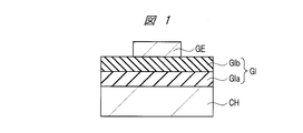
- FIG. 1 is a cross-sectional view illustrating a configuration of a semiconductor device according to a first embodiment.
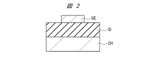
- 4 is a cross-sectional view showing a configuration of a semiconductor device of Comparative Example 1 of Embodiment 1.
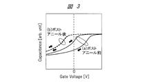
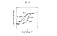
- FIG. 3 is a graph showing capacitance-voltage characteristics of an aluminum oxide film before and after heat treatment. 3 is a graph showing capacitance-voltage characteristics of the gate insulating film of the first embodiment.
- 7 is a cross-sectional view showing a configuration of a semiconductor device of Comparative Example 3 of Embodiment 1.
- FIG. 7 is a cross-sectional view showing a manufacturing step of the semiconductor device of First Embodiment; FIG. FIG.
- FIG. 7 is a cross-sectional view showing a manufacturing step of the semiconductor device of the first embodiment, and is a cross-sectional view showing a manufacturing step following FIG. 6;
- FIG. 8 is a cross-sectional view showing a manufacturing step of the semiconductor device of the first embodiment, and is a cross-sectional view showing a manufacturing step following FIG. 7;
- FIG. 9 is a cross-sectional view showing a manufacturing step of the semiconductor device of the first embodiment, and is a cross-sectional view showing a manufacturing step following FIG. 8;
- FIG. 6 is a cross-sectional view showing another configuration of the semiconductor device of First Embodiment.
- 1 is a cross-sectional view showing a characteristic configuration of a semiconductor device according to a first embodiment.
- FIG. 6 is a cross-sectional view showing a configuration of a semiconductor device according to a second embodiment.
- FIG. 6 is a cross-sectional view illustrating a configuration of a semiconductor device according to a third embodiment.
- 11 is a cross-sectional view showing a manufacturing step of the semiconductor device of Embodiment 3;
- FIG. 15 is a cross-sectional view showing a manufacturing step of the semiconductor device of the third embodiment, and showing the manufacturing step following FIG. 14;
- FIG. 16 is a cross-sectional view showing a manufacturing step of the semiconductor device of the third embodiment, and is a cross-sectional view showing a manufacturing step following FIG. 15;
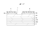
- FIG. 17 is a cross-sectional view showing a manufacturing step of the semiconductor device of the third embodiment, and is a cross-sectional view showing a manufacturing step following FIG. 16;
- FIG. 18 is a cross-sectional view showing a manufacturing step of the semiconductor device of the third embodiment, and showing the manufacturing step following FIG. 17;
- FIG. 19 is a cross-sectional view showing a manufacturing step of the semiconductor device of the third embodiment, and is a cross-sectional view showing a manufacturing step following FIG. 18;
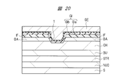
- FIG. 20 is a cross-sectional view showing a manufacturing step of the semiconductor device of the third embodiment, and is a cross-sectional view showing a manufacturing step following FIG. 19.
- FIG. 19 is a cross-sectional view showing a manufacturing step of the semiconductor device of the third embodiment, and is a cross-sectional view showing a manufacturing step following FIG. 19.
- FIG. 19 is a cross-sectional view showing a manufacturing step of the semiconductor device of the third embodiment, and is a cross-sectional view showing
- FIG. 21 is a cross-sectional view showing a manufacturing step of the semiconductor device of the third embodiment, and showing the manufacturing step following FIG. 20;
- FIG. 22 is a cross-sectional view showing a manufacturing step of the semiconductor device of the third embodiment, and showing the manufacturing step following FIG. 21;
- FIG. 23 is a cross-sectional view showing a manufacturing step of the semiconductor device of the third embodiment, and is a cross-sectional view showing a manufacturing step following FIG. 22;
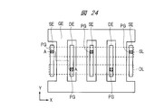
- FIG. 10 is an example of a plan view illustrating a configuration of a semiconductor device according to a third embodiment.
- FIG. 10 is a cross-sectional view showing a configuration of a semiconductor device according to a fourth embodiment.
- the constituent elements are not necessarily indispensable unless otherwise specified or apparently indispensable in principle.
- the shapes when referring to the shapes, positional relationships, etc. of the components, etc., the shapes are substantially the same unless otherwise specified, or otherwise apparent in principle. And the like are included. The same applies to the above numbers and the like (including the number, numerical value, quantity, range, etc.).
- hatching may be omitted even in a cross-sectional view for easy understanding of the drawings. Further, even a plan view may be hatched to make the drawing easy to see.
- each part does not correspond to the actual device, and a specific part may be displayed relatively large for easy understanding of the drawing. Even when the cross-sectional view and the plan view correspond to each other, a specific part may be displayed relatively large in order to make the drawing easy to understand.
- FIG. 1 is a cross-sectional view showing the configuration of the semiconductor device of this embodiment.
- the semiconductor device shown in FIG. 1 is an MIS (Metal Insulator Semiconductor) type field effect transistor (FET) using a nitride semiconductor.
- MIS Metal Insulator Semiconductor
- FET field effect transistor
- the semiconductor device of the present embodiment includes a gate electrode GE disposed on a channel layer CH made of a nitride semiconductor via a gate insulating film GI.
- the gate insulating film GI includes a first gate insulating film GIa formed on the channel layer CH and a second gate insulating film GIb formed on the first gate insulating film GIa.
- the first gate insulating film GIa is made of an oxide of the first metal.
- the second gate insulating film GIb is made of a second metal oxide. The electronegativity of the second metal is lower than the electronegativity of the first metal.
- the first gate insulating film GIa is not a film formed by thermally oxidizing the channel layer (nitride semiconductor) CH, but a film formed by a so-called deposition method (deposition method).
- the first gate insulating film GIa is thicker than the second gate insulating film GIb.
- the film thickness of the first gate insulating film GIa is larger than the film thickness of the second gate insulating film GIb.
- the first metal is, for example, aluminum (Al).
- the oxide of the first metal is aluminum oxide (Al 2 O 3 ).
- the second metal is one or more elements selected from the group of Hf, Zr, Ta, Ti, Nb, La, Y, and Mg.
- the oxide of the second metal is, for example, hafnium oxide (HfO 2 ), zirconium oxide (ZrO), tantalum oxide (Ta 2 O 5 ), titanium oxide (TiO 2 ), niobium oxide (Nb 2 O 5 ). , Lanthanum oxide (La 2 O 3 ), yttrium oxide (Y 2 O 3 ), and magnesium oxide (MgO).
- the composition ratio of the second metal and oxygen is not limited to the above. Moreover, you may contain 2 or more types of elements as a 2nd metal.
- the oxide of the second metal does not include the first metal or a metal element having a lower electronegativity than the first metal.
- the metal having an impurity level may contain a first metal or a metal element having a lower electronegativity than the first metal.
- the threshold voltage (Vth) can be shifted in the positive direction.
- the threshold voltage (Vth) can be positive (Vth> 0) by adjusting the shift amount.
- FIG. 2 is a cross-sectional view showing the configuration of the semiconductor device of Comparative Example 1 of the present embodiment.
- FIG. 3 is a graph showing the capacitance-voltage characteristics of the aluminum oxide film before and after the heat treatment (post-annealing).
- the vertical axis represents the capacitance (Capacitance [arb.unit]), and the horizontal axis represents the gate electrode (Gate Voltage [V]).
- the hysteresis is improved by the heat treatment. That is, the hysteresis is improved in the aluminum oxide film after the heat treatment (graph (b)), while the aluminum oxide film before the heat treatment (graph (a)) shows hysteresis.
- the flat band voltage (Vfb) shifts in the negative direction and Vfb ⁇ 0V.
- the electric conductivity of the second metal constituting the second metal oxide film laminated thereon is higher than the electronegativity of the first metal constituting the first metal oxide film. Since the negative degree is lower, interfacial polarization occurs due to the difference between the two electronegativity. Due to the occurrence of the interface polarization, negative charges are introduced into the oxide film of the first metal, so that the flat band voltage (Vfb) can be shifted in the positive direction. Thereby, the threshold voltage (Vth) that has become negative due to the heat treatment can be shifted in the positive direction. Then, by adjusting the shift amount, it is possible to realize normally-off in which the threshold voltage (Vth) is positive (Vth> 0).
- FIG. 4 is a graph showing the capacitance-voltage characteristics of the gate insulating film of the present embodiment.
- the gate insulating film GI a laminated film of about 100 nm aluminum oxide and hafnium oxide thereon was used.
- the vertical axis represents the capacitance (Capacitance [arb.unit]), and the horizontal axis represents the gate electrode (Gate Voltage [V]).
- FIG. 4 shows a graph when the thickness of the upper hafnium oxide film is 0 nm, 1 nm, 3 nm, and 5 nm.
- the threshold voltage (Vth) is negative (Vth ⁇ 0)
- the film thickness of hafnium oxide is As the value increases in the order of 1 nm, 3 nm, and 5 nm, the threshold voltage (Vth) shifts in the positive direction.
- the oxides of the first metal and the second metal having different electronegativity are stacked and used, and the oxide film of the second metal having a low electronegativity is disposed on the upper layer. It was confirmed that the threshold voltage (Vth) shifted in the positive direction.
- the threshold voltage (Vth) is positive (Vth> 0) when the film thickness of hafnium oxide is 3 nm and 5 nm.
- the film thickness of hafnium oxide (second metal oxide film) is preferably, for example, 1 nm to 10 nm, and more preferably 3 nm to 5 nm. If the hafnium oxide (second metal oxide film) becomes too thick, the total gate insulating film also becomes thick. For this reason, mobility decreases due to a decrease in transistor drive current. In addition, in order to form hafnium oxide (second metal oxide film) unnecessarily thickly, the processing time in the film forming process becomes longer, which causes practical problems such as a decrease in mass productivity and an increase in manufacturing cost. Therefore, the hafnium oxide (second metal oxide film) is preferably thinner than the lower aluminum oxide film (first metal oxide film) and has a thickness of 10 nm or less.
- the lower layer film has an insulating property (leakage current) that is a main characteristic of the gate insulating film.
- a certain thickness for example, 30 nm or more in terms of SiO 2 film thickness, that is, 30 nm or more for an SiO 2 film and 60 nm or more for an Al 2 O 3 film
- oxide film of two metals for example, Zr, Ta, Ti, Nb, La, Y, Mg
- it is preferably 1 nm or more and 10 nm or less, and more preferably 3 nm or more and 5 nm or less.
- the laminated insulating film is a MISFET that uses a gate insulating film
- the MISFET that uses a laminated film of a silicon oxide film (SiO 2 ) on a Si substrate and hafnium oxide (HfO 2 ) thereon as a gate insulating film ( Comparative example 2) can be mentioned.
- the reason why the HfO 2 film, which is a high dielectric constant film, is used as the gate insulating film is to suppress the gate leakage current. That is, if the thickness of the silicon oxide film (SiO 2 ) used as a gate insulating film becomes too thin (for example, 2 nm or less) due to miniaturization of the MISFET, the gate leakage current increases. Therefore, by using a high dielectric constant film, the effective gate insulating film thickness can be increased and the gate leakage current can be reduced.
- the HfO 2 / SiO 2 laminated film is used as the gate insulating film on the Si substrate, a general method of implanting and activating impurity ions into the Si channel can be used for adjusting the threshold voltage.
- a nitride semiconductor particularly GaN
- the threshold voltage cannot be controlled by this method. This is because the activation efficiency is very low even when a p-type impurity is introduced into a nitride semiconductor (GaN), and it is difficult to introduce a high-concentration impurity sufficient to achieve a high threshold. .
- the Si substrate in order to improve the interface state between the Si substrate and the high dielectric constant film, the Si substrate is thermally oxidized to provide SiO 2 . Therefore, the film thickness of the SiO 2 is very thin (e.g., less at 2 nm) are preferably formed. If the film thickness of SiO 2 is too large, it will go against the increase in dielectric constant.
- the SiO 2 film since the SiO 2 film is a film for improving the interface state between the Si substrate and the high dielectric constant film, the Si substrate must be thermally oxidized, for example, CVD (Chemical Vapor) In a film formed by a deposition method such as the Deposition method, the interface state with the Si substrate cannot be improved.
- the first metal oxide film under the gate insulating film of the present embodiment is not obtained by thermally oxidizing the nitride semiconductor layer (which may be a nitride semiconductor substrate) therebelow. That is, the lower oxide film of the first metal is not an oxide of an element constituting the nitride semiconductor layer. In other words, the first metal is different from the elements constituting the nitride semiconductor layer.
- the thermal oxide film of the nitride semiconductor layer does not have a good insulating property and cannot be used as a gate insulating film. Therefore, the first metal oxide film in the lower layer is a film formed by a deposition method such as a CVD method or an ALD (Atomic Layer Deposition) method.
- the lower oxide film of the first metal is formed relatively thick, and has a film thickness of, for example, 30 nm or more.
- the second metal oxide film on the upper layer needs to be made too large because the effect of shifting the flat band voltage (Vfb) in the positive direction is constant above a certain thickness. There is no. For example, a film thickness of 10 nm or less is sufficient. Thus, the upper-layer second metal oxide film is thinner than the lower-layer first metal oxide film.
- FIG. 5 is a cross-sectional view showing the configuration of the semiconductor device of Comparative Example 3 of the present embodiment.
- the MISFET of the present embodiment when the first metal oxide film in the lower layer is formed extremely thin (for example, 2 nm or less) as in Comparative Example 2, the function as the gate insulating film cannot be exhibited.
- the MISFET of Comparative Example 2 when the lower layer film of the gate insulating film is formed by the deposition method such as the CVD method or the ALD method as in the MISFET of the present embodiment, The interface state becomes poor, and the operating characteristics of the MISFET deteriorate.
- the MISFET of Comparative Example 2 when the lower layer film of the gate insulating film is formed relatively thick (for example, 30 nm or more) like the MISFET of the present embodiment, the driving force such as the operation speed is reduced.
- the MISFET of the present embodiment requires a high voltage region breakdown voltage, the total thickness of the gate insulating film is smaller than that of the MISFET of Comparative Example 2 that is miniaturized and driven at a low voltage. Tens of times.
- HfO 2 / SiO 2 of Comparative Example 2 the upper layer, the film thickness of 1nm or less to lower both.
- HfO 2 is about 1 nm to 10 nm, and SiO 2 is about 30 nm to 100 nm.
- the first metal oxide film (first gate insulating film GIa) that is not a film obtained by directly oxidizing the nitride semiconductor layer.
- the second metal oxide film (second gate insulating film GIb) having a lower electronegativity than the first metal shifts the threshold voltage (Vth) in the positive direction. be able to. Then, by adjusting the shift amount, it is possible to realize normally-off in which the threshold voltage (Vth) is positive (Vth> 0).
- FIGS. 6 to 9 are cross-sectional views showing the manufacturing process of the semiconductor device of the present embodiment.
- a substrate on which a channel layer CH is formed is prepared.
- the channel layer CH is a nitride semiconductor layer, and for example, a gallium nitride layer (nGaN layer) containing n-type impurity ions is used.
- nGaN layer gallium nitride layer containing n-type impurity ions
- An nGaN substrate may be used as the substrate, and this substrate may be used as the channel layer CH.
- an nGaN layer may be heteroepitaxially grown on a support substrate such as a Si substrate by using a metal-organic chemical vapor deposition (MOCVD) method, and the nGaN layer may be used as a channel layer CH. .
- MOCVD metal-organic chemical vapor deposition
- the surface of the channel layer (nGaN layer, nGaN substrate) CH is cleaned using a diluted HCl solution or the like.
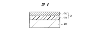
- the gate insulating film GI including the first gate insulating film GIa and the second gate insulating film GIb is formed on the channel layer CH.
- a first gate insulating film (first metal oxide film) GIa is formed on the channel layer CH.
- an aluminum oxide film (Al 2 O 3 film) is deposited as the first gate insulating film GIa by using a deposition method.
- trimethylaluminum (Al (CH 3 ) 3 , TMA) and H 2 O (oxidizing agent) are used as source gases, and an aluminum oxide film having a thickness of about 100 nm is formed using an ALD method in an atmosphere of 400 ° C. Al 2 O 3 film) is deposited.
- the ALD method it is possible to form a film having good controllability and covering property and good film quality.
- ozone (O 3 ) or oxygen (O 2 ) may be used as the oxidizing agent in addition to H 2 O.
- film growth proceeds by two steps of an adsorption reaction and an oxidation reaction.
- TMA and H 2 O generate aluminum oxide (Al 2 O 3 ) and deposit it on the substrate, whereas in the ALD method, TMA is first adsorbed on the surface of the underlying film, and H 2 By reacting with O, the step of forming a layer of aluminum oxide (Al 2 O 3 ) is repeated, and the layer thickness increases.
- heat treatment is performed.
- heat treatment is performed at 750 ° C. for about 1 minute in a nitrogen (N 2 ) atmosphere.
- N 2 nitrogen
- the traps (defects) in the first gate insulating film GIa here, an aluminum oxide film
- the trap density in the film increases, and as described above, the hysteresis of the capacitance-voltage characteristic (CV characteristic) increases (graph in FIG. 3). (See (a)).
- the trap density can be reduced and the hysteresis can be improved.
- a hafnium oxide film (HfO 2 ) is formed on the first gate insulating film GIa (here, the aluminum oxide film) as, for example, a second gate insulating film (second metal oxide film) GIb. Film).
- a hafnium oxide film is deposited by a reactive sputtering method using a Hf metal target and a mixed gas of argon (Ar) and oxygen (O 2 ).
- the film thickness of the hafnium oxide film is preferably about 1 to 10 nm.
- the threshold potential (Vth) of the semiconductor device of this embodiment is, for example, about +1 to + 4V.
- the thickness of the hafnium oxide film may be set larger than the above range.
- the reactive sputtering method is a kind of PVD method.
- an ALD method or a CVD method may be used in addition to the PVD (Physical Vapor Deposition) method.
- heat treatment is performed.
- heat treatment is performed at 750 ° C. for about 1 minute in a nitrogen (N 2 ) atmosphere.
- N 2 nitrogen
- the heat treatment after the formation of the first gate insulating film GIa (aluminum oxide film) and the heat treatment after the formation of the second gate insulating film GIb (hafnium oxide film) are performed separately.
- the heat treatment after the formation of the first gate insulating film GIa is omitted, and the heat treatment is collectively performed after the formation of the laminated film of the first gate insulating film GIa (aluminum oxide film) and the second gate insulating film GIb (hafnium oxide film). You may go.
- the gate insulating film GI having a laminated film of the first gate insulating film GIa (aluminum oxide film) and the second gate insulating film GIb (hafnium oxide film) is formed.
- a gate electrode GE is formed on the gate insulating film GI.
- a titanium nitride (TiN) film for example, is formed as a conductive film on the gate insulating film GI.
- a titanium nitride film with a thickness of about 100 nm is deposited by a reactive sputtering method using a Ti metal target and a mixed gas of argon (Ar) and nitrogen (N 2 ).
- an ALD method or a CVD method may be used in addition to the PVD method.
- the gate electrode GE is formed by patterning the titanium nitride film using a photolithography technique and an etching technique.
- the lower gate insulating film GI may be etched.
- a metal or a metal compound such as Ti, Ta, TaN, Au, Al, W, WN, Ir, Pt, or Ru may be used as a material for forming the gate electrode GE.
- a film in which two or more of these metals or metal compounds are stacked may be used.
- the first metal oxide film and the second metal oxide film having a lower electronegativity than the first metal are stacked and used as the gate insulating film.
- Vth can be shifted in the positive direction.
- the threshold voltage (Vth) shifted in the negative direction can be returned to the positive direction.
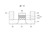
- FIG. 10 is a cross-sectional view showing another configuration of the semiconductor device of the present embodiment.
- FIG. 11 is a cross-sectional view showing a characteristic configuration of the semiconductor device of the present embodiment.
- the semiconductor device of the present embodiment has a gate electrode GE formed on a channel layer (nitride semiconductor) CH via a gate insulating film GI.
- the gate insulating film GI includes a first metal M1 oxide film M1O formed on the channel layer (nitride semiconductor) CH and a second metal M2 oxide film M2O formed on the oxide film M1O. It goes without saying that the composition ratio of M1 and O and the composition ratio of M2 and O vary depending on the selected element.
- the electronegativity of the second metal M2 is smaller than the electronegativity of the first metal M1.
- the first metal M1 and the second metal are selected from Group 2, Group 3, Group 4, Group 5, and Group 13 shown in Table 1 below (Pauling electronegativity).
- the oxide exists in a solid state at a device operating range temperature (for example, ⁇ 200 ° C.), and is a thin film and has good insulating properties.
- a combination of a lower oxide film and an upper oxide film may be selected from the relationship of electronegativity.
- the first metal M1 that is, the metal (element) constituting the lower oxide film
- Al is preferable.
- Si Group 14
- Si may be used as described in the second embodiment and the like described later. If the surface of the nitride semiconductor is oxidized during the formation of the first metal oxide, an interface oxide layer having low insulating properties is formed, and the characteristics of the gate insulating film are impaired.
- the Al oxide that is, aluminum oxide, is suitable for use as a lower layer because it is difficult to form this interface reaction layer even if it is formed on a nitride semiconductor (particularly GaN).
- a first metal oxide film for example, an aluminum oxide film
- a gate is used.
- Si semiconductor
- Si semiconductor
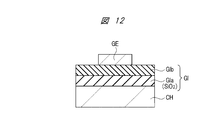
- FIG. 12 is a cross-sectional view showing the configuration of the semiconductor device of this embodiment.
- the gate electrode GE arranged on the channel layer CH made of a nitride semiconductor via the gate insulating film GI.
- the gate insulating film GI includes a silicon oxide film (SiO 2 ) that is the first gate insulating film GIa formed on the channel layer CH, and a second gate insulating film formed on the first gate insulating film GIa. (Second metal oxide film) GIb.
- Si is used in place of the first metal of the first embodiment.
- the first gate insulating film GIa is made of an oxide of Si that is a semiconductor.
- the second gate insulating film GIb is made of a second metal oxide.
- the electronegativity of the second metal is lower than that of Si (semiconductor).
- the silicon oxide film as the first gate insulating film GIa is not a film formed by thermally oxidizing the channel layer (nitride semiconductor) CH, but a film formed by a so-called deposition method (deposition method). is there. That is, the lower Si oxide film is not an oxide of an element constituting the nitride semiconductor layer. Thus, since the Si oxide film is not formed by direct oxidation of the channel layer (nitride semiconductor), Si is different from the elements constituting the channel layer (nitride semiconductor).
- the silicon oxide film as the first gate insulating film GIa is thicker than the second gate insulating film GIb.
- the thickness of the silicon oxide film that is the first gate insulating film GIa is larger than the thickness of the second gate insulating film GIb.
- the film thickness of the first gate insulating film GIa is preferably 30 nm or more, for example.
- the film thickness of the second gate insulating film GIb (second metal oxide film) hafnium oxide (second metal oxide film) is, for example, preferably from 1 nm to 10 nm, and more preferably from 3 nm to 5 nm.
- the second metal is one or more elements selected from the group consisting of Al, Hf, Zr, Ta, Ti, Nb, La, Y, and Mg.
- the oxide of the second metal is, for example, aluminum oxide (Al 2 O 3 ), hafnium oxide (HfO 2 ), zirconium oxide (ZrO), tantalum oxide (Ta 2 O 5 ), titanium oxide (TiO 2 ).
- the composition ratio of the second metal and oxygen is not limited to the above. Moreover, you may contain 2 or more types of elements as a 2nd metal.
- both of the two or more elements must be lower than the electronegativity of Si.
- the oxide of the second metal does not contain Si or a metal element having a lower electronegativity than Si.
- a metal having an impurity level (for example, a metal of 0.01% or less) may contain Si or a metal element having a lower electronegativity than Si.
- the gate insulating film GI is formed by stacking Si and second metal oxides having different electronegativity, and the second layer having a lower electronegativity than Si in the upper layer. Since the metal oxide film is disposed, the threshold voltage (Vth) can be shifted in the positive direction as in the first embodiment.
- the silicon oxide film (SiO 2 ) is used as the first gate insulating film GIa, compared with the case where the aluminum oxide (Al 2 O 3 ) described in the first embodiment is used, The effect of shifting the threshold voltage (Vth) in the positive direction is large. That is, since the electronegativity of Si and Al has a relationship of Al ⁇ Si (see Table 1), when the same oxide film of the second metal (excluding Al) is used as the second gate insulating film GIb, Si The relationship between the electronegativity of Al and the second metal is the relationship of second metal ⁇ Al ⁇ Si.
- the difference in electronegativity is larger in the combination of the second metal and Si than in the combination of the second metal and Al.
- the origin of the interfacial polarization described in Embodiment 1 is the difference in electronegativity, and the larger the difference, the greater the amount of interfacial polarization. Therefore, when the silicon oxide film (SiO 2 ) is used as the lower gate insulating film (GIa), the threshold voltage (Vth) is shifted in the positive direction as compared with the case where aluminum oxide (Al 2 O 3 ) is used. The effect is increased.
- a silicon oxide film is suitable for use as a lower layer of the gate insulating film GI because it is a thin film and has good insulating properties.
- the manufacturing method of the semiconductor device of this embodiment is the same as that of Embodiment 1 except that a silicon oxide film is formed as the first gate insulating film GIa instead of the oxide film of the first metal.
- the surface of the channel layer (nGaN layer, nGaN substrate) CH is cleaned, and a silicon oxide film (SiO 2 film) is formed as the first gate insulating film GIa on the channel layer CH. Deposit using the deposition method.
- a film having a thickness of about 50 nm is formed using trisdimethylaminosilane (SiH (N (CH 3 ) 2 ) 3 , TDMAS) and ozone (O 3 , oxidizing agent) as source gases in an atmosphere of 480 ° C. using an ALD method.
- a thick silicon oxide film (SiO 2 film) is deposited.
- a silicon oxide film may be deposited using a CVD method (thermal CVD, plasma CVD method, or the like).
- the ALD method it is possible to form a film having good controllability and covering property and good film quality.
- film growth proceeds by two steps of an adsorption reaction and an oxidation reaction.
- TDMAS and ozone generate silicon oxide (SiO 2 ) and are deposited on the substrate, whereas in the ALD method, TDMAS is first adsorbed on the surface of the underlying film and reacts with ozone. The process of forming a silicon oxide (SiO 2 ) layer is repeatedly performed, and the layer thickness is increased.
- heat treatment is performed.
- heat treatment is performed at 750 ° C. for about 30 minutes in a nitrogen (N 2 ) atmosphere.
- N 2 nitrogen
- a hafnium oxide film (HfO 2 film) is formed on the first gate insulating film GIa (here, the silicon oxide film) as the second gate insulating film GIb.
- a hafnium oxide film is deposited by a reactive sputtering method using a Hf metal target and a mixed gas of argon (Ar) and oxygen (O 2 ).
- the thickness of the hafnium oxide film varies depending on the threshold potential (Vth), but is preferably about 1 to 10 nm.
- the reactive sputtering method is a kind of PVD method.
- an ALD method or a CVD method may be used.
- heat treatment is performed.
- heat treatment is performed at 750 ° C. for about 1 minute in a nitrogen (N 2 ) atmosphere.
- N 2 nitrogen
- the heat treatment after the formation of the first gate insulating film GIa (silicon oxide film) and the heat treatment after the formation of the second gate insulating film GIb (hafnium oxide film) are performed separately.
- the heat treatment after the formation of the first gate insulating film GIa is omitted, and the heat treatment is collectively performed after the formation of the laminated film of the first gate insulating film GIa (silicon oxide film) and the second gate insulating film GIb (hafnium oxide film). You may go.
- the gate insulating film GI having a laminated film of the first gate insulating film GIa (silicon oxide film) and the second gate insulating film GIb (hafnium oxide film) is formed.
- Hf was illustrated as a 2nd metal
- a 2nd metal is 1 or more elements chosen from the group of Al, Hf, Zr, Ta, Ti, Nb, La, Y, Mg, for example.
- an oxide of one or more elements selected from the group consisting of Al, Hf, Zr, Ta, Ti, Nb, La, Y, and Mg may be used as the second metal oxide.
- the gate electrode GE is formed on the gate insulating film GI.
- the threshold voltage (Vth) is increased in the positive direction by stacking the silicon oxide film and the second metal oxide film having a lower electronegativity than Si and using it as the gate insulating film. Can be shifted.
- the threshold voltage (Vth) shifted in the negative direction can be returned to the positive direction.
- the source region SR and the drain region DR are formed by introducing n-type or p-type impurities into the channel layer (nitride semiconductor) CH on both sides of the gate electrode GE. Furthermore, a source electrode SE and a drain electrode DE may be provided on the source region SR and the drain region DR, respectively (see FIG. 10).
- FIG. 13 is a cross-sectional view showing the configuration of the semiconductor device of this embodiment.
- the semiconductor device shown in FIG. 13 is a MISFET using a nitride semiconductor. This semiconductor device is also called a high electron mobility transistor (HEMT) or a power transistor.
- the semiconductor device of this embodiment is a so-called recess gate type semiconductor device.
- the semiconductor device of the present embodiment has a plurality of nitride semiconductor layers formed on the substrate S. Specifically, a nucleation layer NUC, a strain relaxation layer STR, a buffer layer BU, a channel layer (also referred to as an electron transit layer) CH, and a barrier layer BA are sequentially formed on the substrate S.
- the gate electrode GE is formed through a gate insulating film GI in a trench (also referred to as a trench or a recess) T that penetrates the insulating film IF and the barrier layer BA and is dug in the middle of the channel layer CH.
- the gate insulating film GI includes a first gate insulating film GIa formed on the channel layer CH and a second gate insulating film GIb formed on the first gate insulating film GIa.
- the first gate insulating film GIa is made of an oxide of the first metal.
- the second gate insulating film GIb is made of a second metal oxide. The electronegativity of the second metal is lower than the electronegativity of the first metal.
- the source electrode SE and the drain electrode DE are formed on the barrier layer BA on both sides of the gate electrode GE.
- the silicon oxide film as the first gate insulating film GIa is not a film formed by thermally oxidizing the channel layer (nitride semiconductor) CH, but a film formed by a so-called deposition method (deposition method). is there. That is, the lower oxide film of the first metal is not an oxide of an element constituting the nitride semiconductor layer. Thus, since the oxide film of the first metal is not formed by direct oxidation of the channel layer (nitride semiconductor), the first metal is different from the element constituting the channel layer (nitride semiconductor).
- the first metal oxide film, which is the first gate insulating film GIa is thicker than the second gate insulating film GIb.
- the thickness of the first metal oxide film which is the first gate insulating film GIa is larger than the thickness of the second gate insulating film GIb.
- the film thickness of the first gate insulating film GIa is preferably, for example, 30 nm or more.
- the film thickness of the second gate insulating film GIb is, for example, preferably from 1 nm to 10 nm, and more preferably from 3 nm to 5 nm.
- the second metal is one or more elements selected from the group of Hf, Zr, Ta, Ti, Nb, La, Y, and Mg.
- the oxide of the second metal is, for example, hafnium oxide (HfO 2 ), zirconium oxide (ZrO), tantalum oxide (Ta 2 O 5 ), titanium oxide (TiO 2 ), niobium oxide (Nb 2 O 5 ). , Lanthanum oxide (La 2 O 3 ), yttrium oxide (Y 2 O 3 ), and magnesium oxide (MgO).
- the composition ratio of the second metal and oxygen is not limited to the above. Moreover, you may contain 2 or more types of elements as a 2nd metal.
- the oxide of the second metal does not include the first metal or a metal element having a lower electronegativity than the first metal.
- the metal having an impurity level may contain the first metal or a metal element having a lower electronegativity than the first metal.
- the nucleation layer NUC is formed on the substrate S, and the strain relaxation layer STR is formed on the nucleation layer NUC.
- the nucleation layer NUC is formed in order to generate crystal nuclei when a layer formed on the strain relaxation layer STR or the like grows. Further, it is formed to prevent the constituent elements (for example, Ga, etc.) of the layer formed in the upper part from diffusing from the layer formed in the upper part into the substrate S to change the quality of the substrate S.
- the strain relaxation layer STR is formed in order to relieve stress on the substrate S and suppress the occurrence of warpage and cracks in the substrate S.
- a buffer layer BU is formed on the strain relaxation layer STR, a channel layer (also referred to as an electron transit layer) CH made of a nitride semiconductor is formed on the buffer layer BU, and a nitride semiconductor is formed on the channel layer CH.
- a barrier layer BA is formed.
- a source electrode SE and a drain electrode DE are formed on the barrier layer BA.
- the source electrode SE and drain electrode DE and the barrier layer BA are ohmically connected to each other.
- An insulating layer IL1 is formed on the gate electrode GE, the source electrode SE, and the drain electrode DE. Of the insulating layer IL1, the insulating layer IL1 over the source electrode SE and the drain electrode DE is removed to form a contact hole.
- a conductive film is embedded in the contact hole, and a wiring M is formed thereon.
- An insulating layer IL2 is formed on the wiring M.
- the two-dimensional electron gas 2DEG is generated on the channel layer side near the interface between the channel layer CH and the barrier layer BA.
- a positive potential threshold potential
- a channel C is formed in the vicinity of the interface between the gate electrode GE and the channel layer CH.
- the 2D electron gas 2DEG is formed by the following mechanism.
- Nitride semiconductors here, gallium nitride-based semiconductors
- the channel layer CH and the barrier layer BA have different forbidden bandwidths (band gaps) and electron affinities, respectively. For this reason, a well-type potential is generated at the junction surface of these semiconductors. By accumulating electrons in the well-type potential, a two-dimensional electron gas 2DEG is generated in the vicinity of the interface between the channel layer CH and the barrier layer BA.
- the two-dimensional electron gas 2DEG formed in the vicinity of the interface between the channel layer CH and the barrier layer BA is divided by the groove T in which the gate electrode GE is formed. For this reason, in the semiconductor device of the present embodiment, on / off can be switched depending on whether or not the channel C is formed.
- the gate insulating film GI since the stacked film of the first metal oxide and the second metal oxide having a lower electronegativity than the first metal disposed thereon is used as the gate insulating film GI.
- the flat band voltage (Vfb) can be shifted in the positive direction.
- the threshold voltage (Vth) can be shifted in the positive direction.
- the threshold voltage (Vth) can be positive (Vth> 0), and the normally-off characteristic can be improved.
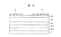
- FIGS. 14 to 23 are cross-sectional views showing the manufacturing process of the semiconductor device of the present embodiment.
- a semiconductor substrate made of silicon (Si) with an exposed (111) surface is used as the substrate S, and a nucleation layer NUC is formed thereon as an nucleation layer NUC.
- the layer is heteroepitaxially grown using a metal organic chemical vapor deposition method or the like.
- a superlattice structure in which a laminated film (AlN / GaN film) of a gallium nitride (GaN) layer and an aluminum nitride (AlN) layer is repeatedly laminated is formed on the nucleation layer NUC as a strain relaxation layer STR. .
- a gallium nitride (GaN) layer and an aluminum nitride (AlN) layer are repeatedly heterogeneous by about 100 layers (total 200 layers) each with a thickness of about 2 to 3 nm using metal organic vapor phase epitaxy. Epitaxially grow.
- a substrate made of SiC, sapphire, or the like may be used in addition to the silicon.
- the buffer layer BU is formed on the strain relaxation layer STR.
- the buffer layer BU for example, an AlGaN layer is heteroepitaxially grown using a metal organic chemical vapor deposition method or the like.
- a channel layer CH is formed on the buffer layer BU.
- a gallium nitride layer (nGaN layer) containing n-type impurity ions is heteroepitaxially grown on the buffer layer BU.
- a gallium nitride layer (nGaN layer) doped with an n-type impurity is heteroepitaxially grown in an atmosphere in which an n-type impurity gas is mixed in a gallium nitride material gas.
- Silane (SiH 4 ) can be used as the n-type impurity gas.
- the electron affinity of the channel layer CH is larger than the electron affinity of the buffer layer BU.
- the channel layer CH is a nitride semiconductor having a narrower band gap than the buffer layer BU.
- barrier layer BA for example, an AlGaN layer is heteroepitaxially grown on the channel layer CH using a metal organic chemical vapor deposition method or the like.
- the electron affinity of the barrier layer BA is smaller than the electron affinity of the channel layer CH.
- the barrier layer BA is a nitride semiconductor having a wider band gap than the channel layer CH.
- a stacked body of the buffer layer BU, the channel layer CH, and the barrier layer BA is formed.
- This stacked body is formed by the above-described heteroepitaxial growth, that is, group III surface growth that is stacked in the [0001] crystal axis (C-axis) direction.
- the stacked body is formed by (0001) Ga surface growth.
- a two-dimensional electron gas 2DEG is generated near the interface between the channel layer CH and the barrier layer BA.
- an insulating film IF having an opening is formed on the barrier layer BA.
- a silicon nitride film is deposited on the barrier layer BA by using a thermal CVD method or the like.
- an opening is formed in the insulating film IF by using a photolithography technique and an etching technique.
- the barrier layer BA and the channel layer CH are etched to form a trench T that penetrates the insulating film IF and the barrier layer BA and reaches the middle of the channel layer CH (FIG. 17).
- heat treatment annealing
- the gate insulating film GI including the first gate insulating film GIa and the second gate insulating film GIb is formed in the trench T and on the insulating film IF.
- the first gate insulating film GIa is formed in the trench T where the channel layer CH is exposed at the bottom and on the insulating film IF.
- an aluminum oxide film Al 2 O 3 film
- Al 2 O 3 film is deposited on the bottom surface, the side wall, and the insulating film IF of the trench T.
- a diluted HCl solution for example, trimethylaluminum (Al (CH 3 ) 3 , TMA) and H 2 O (oxidant) are used as source gases and an atmosphere at 400 ° C.
- an ALD method is used to deposit an aluminum oxide film (Al 2 O 3 film) having a thickness of about 100 nm in the trench T and on the insulating film IF.
- Al 2 O 3 film aluminum oxide film having a thickness of about 100 nm in the trench T and on the insulating film IF.
- the controllability of the film thickness is good, and a film can be formed on the uneven surface with good coverage.
- ozone (O 3 ) or oxygen (O 2 ) may be used as the oxidizing agent in addition to H 2 O.
- heat treatment is performed.
- heat treatment is performed at 750 ° C. for about 1 minute in a nitrogen (N 2 ) atmosphere.
- N 2 nitrogen
- traps (defects) in the first gate insulating film GIa here, an aluminum oxide film
- the trap density in the film increases, and the hysteresis of the capacity-voltage characteristics (CV characteristics) increases. For this reason, trap density can be reduced by performing heat treatment (post-annealing) (see FIG. 3).
- a hafnium oxide film (HfO 2 film) is formed as the second gate insulating film GIb on the first gate insulating film GIa (here, the aluminum oxide film).
- a hafnium oxide film is deposited by a reactive sputtering method using a Hf metal target and a mixed gas of argon (Ar) and oxygen (O 2 ).
- the thickness of the hafnium oxide film varies depending on the threshold potential (Vth), but is preferably about 1 to 10 nm.
- the reactive sputtering method is a kind of PVD method.
- an ALD method or a CVD method may be used.
- heat treatment is performed.
- heat treatment is performed at 750 ° C. for about 1 minute in a nitrogen (N 2 ) atmosphere.
- N 2 nitrogen
- the heat treatment after the formation of the first gate insulating film GIa (aluminum oxide film) and the heat treatment after the formation of the second gate insulating film GIb (hafnium oxide film) are performed separately.
- the heat treatment after the formation of the first gate insulating film GIa is omitted, and the heat treatment is collectively performed after the formation of the laminated film of the first gate insulating film GIa (aluminum oxide film) and the second gate insulating film GIb (hafnium oxide film). You may go.
- the gate insulating film GI having a laminated film of the first gate insulating film GIa (aluminum oxide film) and the second gate insulating film GIb (hafnium oxide film) is formed.
- a gate electrode GE is formed on the gate insulating film GI.
- a titanium nitride (TiN) film for example, is formed as a conductive film (GE) on the gate insulating film GI (FIG. 20).
- a titanium nitride film with a thickness of about 100 nm is deposited by a reactive sputtering method using a Ti metal target and a mixed gas of argon (Ar) and nitrogen (N 2 ).
- an ALD method or a CVD method may be used in addition to the PVD method.
- the gate electrode GE is formed by patterning the titanium nitride film using a photolithography technique and an etching technique (FIG. 21). Note that when the titanium nitride film is etched, the lower gate insulating film GI may be etched.
- a metal or a metal compound such as Ti, Ta, TaN, Au, Al, W, WN, Ir, Pt, or Ru may be used as a material for forming the gate electrode GE. A film in which two or more of these metals or metal compounds are stacked may be used.
- the source electrode SE and the drain electrode DE are formed on the barrier layer BA on both sides of the gate electrode GE.
- a laminated film also referred to as an Al / Ti film
- Al aluminum
- TiN titanium nitride
- the TiN / Ti / Al / Ti film is patterned and, for example, heat treatment is performed at 550 ° C. for about 30 minutes.
- heat treatment is performed at 550 ° C. for about 30 minutes.
- a silicon oxide film is formed as the insulating layer IL1 on the gate electrode GE, the source electrode SE, and the drain electrode DE by using a CVD method or the like.
- the insulating layer IL1 over the source electrode SE and the drain electrode DE is removed by etching to form a contact hole.
- a conductive film is formed on the insulating layer IL1 including the inside of the contact hole.
- an aluminum alloy film is deposited using a sputtering method or the like.
- the aluminum alloy for example, an alloy of Al and Si (Al—Si), an alloy of Al and Cu (copper) (Al—Cu), Al, Si and Cu (Al—Si—Cu), or the like may be used. It can.
- the aluminum alloy film is patterned to form the conductive film (plug) in the contact hole and the wiring M thereon.
- an insulating layer (also referred to as a cover film or a surface protective film) IL2 is formed on the insulating layer IL1 including the source electrode SE and the drain electrode DE.
- a silicon oxynitride (SiON) film is deposited using a CVD method or the like (see FIG. 13).
- the semiconductor device of this embodiment can be formed.
- the first metal oxide film and the second metal oxide film having a lower electronegativity than the first metal are stacked and used as the gate insulating film.
- Vth can be shifted in the positive direction. Then, by adjusting the shift amount, it is possible to realize normally-off in which the threshold voltage (Vth) is positive (Vth> 0).
- the threshold voltage (Vth) shifted in the negative direction can be returned to the positive direction.
- FIG. 24 is an example of a plan view showing the configuration of the semiconductor device of this embodiment.
- FIG. 13 corresponds to the AA cross section of FIG.
- the source electrode SE and the drain electrode DE are, for example, in a line shape extending in the Y direction. In other words, it is a rectangular shape (rectangular shape) having long sides in the Y direction.
- the source electrode SE and the drain electrode DE are alternately arranged in the X direction.
- the gate electrode GE is disposed between the source electrode SE and the drain electrode DE.
- one end (upper side in the drawing) of a plurality of line-shaped gate electrode portions (GE) extending in the Y direction is connected to a line (also referred to as a gate line) extending in the X direction.
- the other end (lower side in the figure) of the plurality of line-shaped gate electrode portions (GE) extending in the Y direction is connected to a line (also referred to as a gate line) extending in the X direction.
- a line also referred to as a gate line
- one of the two lines (also referred to as gate lines) extending in the X direction may be omitted, and the gate electrode GE may have a comb shape.
- the plurality of source electrodes SE are connected to a source line SL extending in the X direction via a plug (connection portion) PG.
- the plurality of drain electrodes DE are connected to a drain line DL extending in the X direction via a plug (connection portion) PG.
- the source line SL, the drain line DL, and the wiring M correspond to each other.
- a first metal oxide film for example, an aluminum oxide film
- a gate is used.
- Si semiconductor is used as an element constituting the film (GIa) under the insulating film GI.
- FIG. 25 is a cross-sectional view showing the configuration of the semiconductor device of the present embodiment.
- the semiconductor device of this embodiment is a recessed gate type high electron mobility transistor similar to that of the first embodiment.
- the semiconductor device of the present embodiment is the same as that of the third embodiment except that a silicon oxide film is formed as the first gate insulating film GIa instead of the oxide film of the first metal.
- the semiconductor device of the present embodiment has a plurality of nitride semiconductor layers formed on the substrate S as in the case of the third embodiment. Specifically, a nucleation layer NUC, a strain relaxation layer STR, a buffer layer BU, a channel layer (also referred to as an electron transit layer) CH, and a barrier layer BA are sequentially formed on the substrate S.
- the gate electrode GE is formed through a gate insulating film GI in a trench (also referred to as a trench or a recess) T that penetrates the insulating film IF and the barrier layer BA and is dug in the middle of the channel layer CH.
- the gate insulating film GI includes a first gate insulating film GIa formed on the channel layer CH and a second gate insulating film GIb formed on the first gate insulating film GIa.
- the first gate insulating film GIa is made of an oxide of Si (semiconductor).
- the second gate insulating film GIb is made of a second metal oxide. The electronegativity of the second metal is lower than that of Si.
- the source electrode SE and the drain electrode DE are formed on the barrier layer BA on both sides of the gate electrode GE.
- the silicon oxide film as the first gate insulating film GIa is not a film formed by thermally oxidizing the channel layer (nitride semiconductor) CH, but a film formed by a so-called deposition method (deposition method). is there. That is, the lower Si oxide film is not an oxide of an element constituting the nitride semiconductor layer. Thus, since the Si oxide film is not formed by direct oxidation of the channel layer (nitride semiconductor), Si is different from the elements constituting the channel layer (nitride semiconductor).
- the silicon oxide film as the first gate insulating film GIa is thicker than the second gate insulating film GIb.
- the thickness of the silicon oxide film that is the first gate insulating film GIa is larger than the thickness of the second gate insulating film GIb.
- the film thickness of the first gate insulating film GIa is preferably 30 nm or more, for example.
- the film thickness of the second gate insulating film GIb is, for example, preferably from 1 nm to 10 nm, and more preferably from 3 nm to 5 nm.
- the second metal is one or more elements selected from the group consisting of Al, Hf, Zr, Ta, Ti, Nb, La, Y, and Mg.
- the oxide of the second metal is, for example, aluminum oxide (Al 2 O 3 ), hafnium oxide (HfO 2 ), zirconium oxide (ZrO), tantalum oxide (Ta 2 O 5 ), titanium oxide (TiO 2 ).
- the composition ratio of the second metal and oxygen is not limited to the above. Moreover, you may contain 2 or more types of elements as a 2nd metal.
- both of the two or more elements must be lower than the electronegativity of Si.
- the oxide of the second metal does not contain Si or a metal element having a lower electronegativity than Si.
- a metal having an impurity level (for example, a metal of 0.01% or less) may contain Si or a metal element having a lower electronegativity than Si.
- the gate insulating film GI is formed by stacking Si and second metal oxides having different electronegativity, and the second layer having a lower electronegativity than Si in the upper layer. Since the metal oxide film is disposed, the threshold voltage (Vth) can be shifted in the positive direction as in the first embodiment.
- the silicon oxide film (SiO 2 ) is used as the first gate insulating film GIa, compared with the case where the aluminum oxide (Al 2 O 3 ) described in the first embodiment is used, The effect of shifting the threshold voltage (Vth) in the positive direction is large. That is, since the electronegativity of Si and Al has a relationship of Al ⁇ Si (see Table 1), when the same oxide film of the second metal (excluding Al) is used as the second gate insulating film GIb, Si The relationship between the electronegativity of Al and the second metal is the relationship of second metal ⁇ Al ⁇ Si.
- the difference in electronegativity is larger in the combination of the second metal and Si than in the combination of the second metal and Al.
- the origin of the interfacial polarization described in Embodiment 1 is the difference in electronegativity, and the larger the difference, the greater the amount of interfacial polarization. Therefore, when the silicon oxide film (SiO 2 ) is used as the lower gate insulating film GIa, the effect of shifting the threshold voltage (Vth) in the positive direction is greater than when aluminum oxide (Al 2 O 3 ) is used. growing.
- the manufacturing method of the semiconductor device of the present embodiment is the same as that of the third embodiment except that a silicon oxide film is formed as the first gate insulating film GIa instead of the oxide film of the first metal.
- the nucleation layer NUC, the strain relaxation layer STR, the buffer layer BU, the channel layer CH, and the barrier layer BA are sequentially formed on the substrate S.
- a constituent material of these layers for example, a material similar to that in Embodiment 3 can be used. Further, these layers can be formed in the same process as in Embodiment Mode 3.
- the electron affinity of the channel layer CH is larger than the electron affinity of the buffer layer BU.
- the channel layer CH is a nitride semiconductor having a narrower band gap than the buffer layer BU.
- the electron affinity of the barrier layer BA is smaller than the electron affinity of the channel layer CH.
- the barrier layer BA is a nitride semiconductor having a wider band gap than the channel layer CH.
- an insulating film IF having an opening is formed on the barrier layer BA, and the trench T is formed by etching the barrier layer BA and the channel layer CH using the insulating film IF as a mask.
- the gate insulating film GI including the first gate insulating film GIa and the second gate insulating film GIb is formed in the trench T and on the insulating film IF.
- the first gate insulating film GIa is formed in the trench T where the channel layer CH is exposed at the bottom and on the insulating film IF.
- a silicon oxide film SiO 2 film
- SiO 2 film is deposited on the bottom surface, the side wall, and the insulating film IF of the trench T.
- a silicon oxide film (SiO 2 film) having a thickness of about 50 nm is deposited in the trench T and on the insulating film IF using the ALD method.
- a silicon oxide film may be deposited using a CVD method (thermal CVD, plasma CVD method, or the like). According to the ALD method, the controllability of the film thickness is good, and a film can be formed on the uneven surface with good coverage.
- heat treatment is performed.
- heat treatment is performed at 750 ° C. for about 1 minute in a nitrogen (N 2 ) atmosphere.
- N 2 nitrogen
- a hafnium oxide film (HfO 2 film) is formed as the second gate insulating film GIb, for example, on the first gate insulating film GIa (here, a silicon oxide film).
- a hafnium oxide film is deposited by a reactive sputtering method using a Hf metal target and a mixed gas of argon (Ar) and oxygen (O 2 ).
- the thickness of the hafnium oxide film varies depending on the threshold potential (Vth), but is preferably about 1 to 10 nm.
- the reactive sputtering method is a kind of PVD method.
- an ALD method or a CVD method may be used.
- heat treatment is performed.
- heat treatment is performed at 750 ° C. for about 1 minute in a nitrogen (N 2 ) atmosphere.
- N 2 nitrogen
- the heat treatment after the formation of the first gate insulating film GIa (silicon oxide film) and the heat treatment after the formation of the second gate insulating film GIb (hafnium oxide film) are performed separately.
- the heat treatment after the formation of the first gate insulating film GIa (silicon oxide film) is omitted. You may heat-process collectively.
- the gate insulating film GI having a laminated film of the first gate insulating film GIa (silicon oxide film) and the second gate insulating film GIb (hafnium oxide film) is formed.
- the gate electrode GE, the source electrode SE, and the drain electrode DE are formed, and further, the insulating layer IL1, the plug, the wiring M, and the insulating layer IL2 are formed (see FIG. 25). .
- the semiconductor device of this embodiment can be formed.
- the threshold voltage (Vth) is set to be positive by stacking the Si oxide film and the second metal oxide film having a lower electronegativity than Si and using it as a gate insulating film. Can shift in the direction. Then, by adjusting the shift amount, it is possible to realize normally-off in which the threshold voltage (Vth) is positive (Vth> 0).
- the threshold voltage (Vth) shifted in the negative direction can be returned to the positive direction.
- the gate insulating film includes an Si oxide film formed on the bottom and side walls of the trench, and a metal oxide film having a lower electronegativity than the Si formed on the Si oxide film. , The Si is a semiconductor device different from an element constituting the second nitride semiconductor layer.
- the Si oxide film is thicker than the metal oxide film having a lower electronegativity than the Si,
- the thickness of the metal oxide film having a lower electronegativity than Si is 1 nm or more and 10 nm or less.
- step (a) is a step of depositing a first metal oxide film on the nitride semiconductor layer, A method of manufacturing a semiconductor device, comprising a step of performing a heat treatment on the oxide film of the first metal after the step (a).
- the method (a) is a method of manufacturing a semiconductor device, wherein the first metal oxide film is deposited by an atomic layer deposition method.
- the oxide film of the first metal is thicker than the oxide film of the second metal, The method of manufacturing a semiconductor device, wherein the oxide film of the second metal has a thickness of 1 nm to 10 nm.
- step (a) is a step of depositing an oxide film of Si on the nitride semiconductor layer, A method of manufacturing a semiconductor device, comprising a step of performing a heat treatment on the Si oxide film after the step (a).
- (Appendix 16) (A) forming a first nitride semiconductor layer above the substrate, forming a second nitride semiconductor layer having a higher electron affinity than the first nitride semiconductor layer on the first nitride semiconductor layer; Forming a third nitride semiconductor layer having a lower electron affinity than the second nitride semiconductor layer on the second nitride semiconductor layer; (B) Etching the third nitride semiconductor layer and the second nitride semiconductor layer to form a groove penetrating the third nitride semiconductor layer and reaching the middle of the second nitride semiconductor layer
- the step (c) is a step of depositing the oxide film of the first metal on
- (Appendix 17) (A) forming a first nitride semiconductor layer above the substrate, forming a second nitride semiconductor layer having a higher electron affinity than the first nitride semiconductor layer on the first nitride semiconductor layer; Forming a third nitride semiconductor layer having a lower electron affinity than the second nitride semiconductor layer on the second nitride semiconductor layer; (B) Etching the third nitride semiconductor layer and the second nitride semiconductor layer to form a groove penetrating the third nitride semiconductor layer and reaching the middle of the second nitride semiconductor layer
- the step (c) is a step of depositing the Si oxide film on the bottom and side walls of the groove, A method
- 2DEG two-dimensional electron gas BA barrier layer BU buffer layer C channel CH channel layer DE drain electrode DR drain region GE gate electrode GI gate insulating film GIa first gate insulating film GIb second gate insulating film IF insulating film IL1 insulating layer IL2 insulating layer M wiring M1 first metal M1O oxide film M2 second metal M2O oxide film NUC nucleation layer Ox oxide film SE source electrode SR source region STR strain relaxation layer T groove
Landscapes
- Insulated Gate Type Field-Effect Transistor (AREA)
- Thin Film Transistor (AREA)
- Electrodes Of Semiconductors (AREA)
- Junction Field-Effect Transistors (AREA)
Abstract
Description
以下、図面を参照しながら本実施の形態の半導体装置について詳細に説明する。
図1は、本実施の形態の半導体装置の構成を示す断面図である。図1に示す半導体装置は、窒化物半導体を用いたMIS(Metal Insulator Semiconductor)型の電界効果トランジスタ(FET;Field Effect Transistor)である。
次いで、図6~図9を参照しながら、本実施の形態の半導体装置の製造方法を説明するとともに、当該半導体装置の構成をより明確にする。図6~図9は、本実施の形態の半導体装置の製造工程を示す断面図である。

実施の形態1(図1)においては、ゲート絶縁膜GIの下層の膜(GIa)として、第1金属の酸化膜(例えば、酸化アルミニウム膜)を用いたが、本実施の形態においては、ゲート絶縁膜GIの下層の膜(GIa)を構成する元素として、Si(半導体)を用いる。
図12は、本実施の形態の半導体装置の構成を示す断面図である。図12に示すように、本実施の形態の半導体装置においては、実施の形態1の場合と同様に、窒化物半導体よりなるチャネル層CH上にゲート絶縁膜GIを介して配置されたゲート電極GEを有する。ここで、ゲート絶縁膜GIは、チャネル層CH上に形成された第1ゲート絶縁膜GIaである酸化シリコン膜(SiO2)と、第1ゲート絶縁膜GIa上に形成された第2ゲート絶縁膜(第2金属の酸化膜)GIbとを有する。このように、実施の形態1の第1金属に代えてSiが用いられている。即ち、第1ゲート絶縁膜GIaは、半導体であるSiの酸化物よりなる。第2ゲート絶縁膜GIbは、第2金属の酸化物よりなる。そして、第2金属の電気陰性度は、Si(半導体)の電気陰性度より低い。
次いで、本実施の形態の半導体装置の製造方法を説明する。本実施の形態の半導体装置の製造方法においては、第1ゲート絶縁膜GIaとして、第1金属の酸化膜に代えて酸化シリコン膜を形成する以外は実施の形態1の場合と同様である。
以下、図面を参照しながら本実施の形態の半導体装置について詳細に説明する。
図13は、本実施の形態の半導体装置の構成を示す断面図である。図13に示す半導体装置は、窒化物半導体を用いたMISFETである。この半導体装置は、高電子移動度トランジスタ(HEMT:High Electron Mobility Transistor)やパワートランジスタとも呼ばれる。本実施の形態の半導体装置は、いわゆるリセスゲート型の半導体装置である。
次いで、図14~図23を参照しながら、本実施の形態の半導体装置の製造方法を説明するとともに、当該半導体装置の構成をより明確にする。図14~図23は、本実施の形態の半導体装置の製造工程を示す断面図である。
実施の形態3(図13)においては、ゲート絶縁膜GIの下層の膜(GIa)として、第1金属の酸化膜(例えば、酸化アルミニウム膜)を用いたが、本実施の形態においては、ゲート絶縁膜GIの下層の膜(GIa)を構成する元素として、Si(半導体)を用いる。
図25は、本実施の形態の半導体装置の構成を示す断面図である。図25に示すように、本実施の形態の半導体装置は、実施の形態1と同様のリセスゲート型の高電子移動度トランジスタである。本実施の形態の半導体装置においては、第1ゲート絶縁膜GIaとして、第1金属の酸化膜に代えて酸化シリコン膜を形成する以外は実施の形態3の場合と同様である。
次いで、本実施の形態の半導体装置の製造方法を説明する。本実施の形態の半導体装置の製造方法においては、第1ゲート絶縁膜GIaとして、第1金属の酸化膜に代えて酸化シリコン膜を形成する以外は実施の形態3の場合と同様である。
基板の上方に形成された第1窒化物半導体層と、
前記第1窒化物半導体層上に形成された第2窒化物半導体層と、
前記第2窒化物半導体層上に形成された第3窒化物半導体層と、
前記第3窒化物半導体層を貫通し、前記第2窒化物半導体層まで到達する溝と、
前記溝内にゲート絶縁膜を介して配置されたゲート電極と、
を有し、
前記第3窒化物半導体層の電子親和力は、前記第2窒化物半導体層の電子親和力より小さく、
前記第2窒化物半導体層の電子親和力は、前記第1窒化物半導体層の電子親和力より大きく、
前記ゲート絶縁膜は、前記溝の底面および側壁上に形成されたSiの酸化膜と、前記Siの酸化膜上に形成された前記Siより電気陰性度が低い金属の酸化膜と、を有し、
前記Siは、第2窒化物半導体層を構成する元素と異なる、半導体装置。
付記1記載の半導体装置において、
前記Siの酸化膜は、堆積膜である、半導体装置。
付記2記載の半導体装置において、
前記堆積膜は、原子層堆積法により形成された膜である、半導体装置。
付記1記載の半導体装置において、
前記第2金属は、Al、Hf、Zr、Ta、Ti、Nb、La、Y、Mgの群から選ばれる1以上の元素である、半導体装置。
付記4記載の半導体装置において、
前記第2窒化物半導体層は、GaNである、半導体装置。
付記1記載の半導体装置において、
前記Siの酸化膜は、前記Siより電気陰性度が低い金属の酸化膜より厚い、半導体装置。
付記1記載の半導体装置において、
前記Siの酸化膜は、前記Siより電気陰性度が低い金属の酸化膜より厚く、
前記Siより電気陰性度が低い金属の酸化膜の膜厚は、1nm以上10nm以下である、半導体装置。
(a)窒化物半導体層上に、第1金属の酸化膜を形成する工程、
(b)前記第1金属の酸化膜上に、前記第1金属より電気陰性度が低い第2金属の酸化膜を形成する工程、
(c)前記第2金属の酸化膜上に、ゲート電極を形成する工程、
を有し、
前記(a)工程は、第1金属の酸化膜を窒化物半導体層上に堆積させる工程であり、
前記(a)工程の後、前記第1金属の酸化膜に対し熱処理を施す工程、を有する、半導体装置の製造方法。
付記8記載の半導体装置の製造方法において、
前記(a)工程は、原子層堆積法により、前記第1金属の酸化膜を堆積する工程である、半導体装置の製造方法。
付記8記載の半導体装置の製造方法において、
前記第1金属は、Alである、半導体装置の製造方法。
付記10記載の半導体装置の製造方法において、
前記第2金属は、Hf、Zr、Ta、Ti、Nb、La、Y、Mgの群から選ばれる1以上の元素である、半導体装置の製造方法。
付記11記載の半導体装置の製造方法において、
前記窒化物半導体層は、GaNである、半導体装置の製造方法。
付記8記載の半導体装置の製造方法において、
前記第1金属の酸化膜は、前記第2金属の酸化膜より厚い、半導体装置の製造方法。
付記8記載の半導体装置の製造方法において、
前記第1金属の酸化膜は、前記第2金属の酸化膜より厚く、
前記第2金属の酸化膜の膜厚は、1nm以上10nm以下である、半導体装置の製造方法。
(a)窒化物半導体層上に、Siの酸化膜を形成する工程、
(b)前記Siの酸化膜上に、前記Siより電気陰性度が低い金属の酸化膜を形成する工程、
(c)前記Siより電気陰性度が低い金属の酸化膜上に、ゲート電極を形成する工程、
を有し、
前記(a)工程は、Siの酸化膜を窒化物半導体層上に堆積させる工程であり、
前記(a)工程の後、前記Siの酸化膜に対し熱処理を施す工程、を有する、半導体装置の製造方法。
(a)基板の上方に第1窒化物半導体層を形成し、前記第1窒化物半導体層上に、前記第1窒化物半導体層より電子親和力が大きい第2窒化物半導体層を形成し、前記第2窒化物半導体層上に、前記第2窒化物半導体層より電子親和力が小さい第3窒化物半導体層を形成する工程、
(b)前記第3窒化物半導体層および前記第2窒化物半導体層をエッチングすることにより、前記第3窒化物半導体層を貫通し、前記第2窒化物半導体層の途中まで到達する溝を形成する工程、
(c)前記溝の底面および側壁上に第1金属の酸化膜を形成する工程、
(d)前記第1金属の酸化膜上に、前記第1金属より電気陰性度が低い第2金属の酸化膜を形成する工程、
(e)前記第2金属の酸化膜上に、ゲート電極を形成する工程、
を有し、
前記(c)工程は、前記第1金属の酸化膜を前記溝の底面および側壁上に堆積させる工程であり、
前記(c)工程の後、前記第1金属の酸化膜に対し熱処理を施す工程を有する、半導体装置の製造方法。
(a)基板の上方に第1窒化物半導体層を形成し、前記第1窒化物半導体層上に、前記第1窒化物半導体層より電子親和力が大きい第2窒化物半導体層を形成し、前記第2窒化物半導体層上に、前記第2窒化物半導体層より電子親和力が小さい第3窒化物半導体層を形成する工程、
(b)前記第3窒化物半導体層および前記第2窒化物半導体層をエッチングすることにより、前記第3窒化物半導体層を貫通し、前記第2窒化物半導体層の途中まで到達する溝を形成する工程、
(c)前記溝の底面および側壁上にSiの酸化膜を形成する工程、
(d)前記Siの酸化膜上に、前記Siより電気陰性度が低い金属の酸化膜を形成する工程、
(e)前記金属の酸化膜上に、ゲート電極を形成する工程、
を有し、
前記(c)工程は、前記Siの酸化膜を前記溝の底面および側壁上に堆積させる工程であり、
前記(c)工程の後、前記Siの酸化膜に対し熱処理を施す工程を有する、半導体装置の製造方法。
BA 障壁層
BU バッファ層
C チャネル
CH チャネル層
DE ドレイン電極
DR ドレイン領域
GE ゲート電極
GI ゲート絶縁膜
GIa 第1ゲート絶縁膜
GIb 第2ゲート絶縁膜
IF 絶縁膜
IL1 絶縁層
IL2 絶縁層
M 配線
M1 第1金属
M1O 酸化膜
M2 第2金属
M2O 酸化膜
NUC 核生成層
Ox 酸化膜
SE ソース電極
SR ソース領域
STR 歪緩和層
T 溝
Claims (23)
- 窒化物半導体層と、
前記窒化物半導体層上にゲート絶縁膜を介して形成されたゲート電極と、
を有し、
前記ゲート絶縁膜は、前記窒化物半導体層上に形成された第1金属の酸化膜と、前記第1金属の酸化膜上に形成された第2金属の酸化膜と、を有し、
前記第1金属は、前記窒化物半導体層を構成する元素と異なり、
前記第2金属は、前記第1金属より電気陰性度が低い、半導体装置。 - 請求項1記載の半導体装置において、
前記第1金属の酸化膜は、堆積膜である、半導体装置。 - 請求項2記載の半導体装置において、
前記堆積膜は、原子層堆積法により形成された膜である、半導体装置。 - 請求項1記載の半導体装置において、
前記第1金属は、Alである、半導体装置。 - 請求項4記載の半導体装置において、
前記第2金属は、Hf、Zr、Ta、Ti、Nb、La、Y、Mgの群から選ばれる1以上の元素である、半導体装置。 - 請求項5記載の半導体装置において、
前記窒化物半導体層は、GaNである、半導体装置。 - 請求項1記載の半導体装置において、
前記第1金属の酸化膜は、前記第2金属の酸化膜より厚い、半導体装置。 - 請求項1記載の半導体装置において、
前記第1金属の酸化膜は、前記第2金属の酸化膜より厚く、
前記第2金属の酸化膜の膜厚は、1nm以上10nm以下である、半導体装置。 - 窒化物半導体層と、
前記窒化物半導体層上にゲート絶縁膜を介して形成されたゲート電極と、
を有し、
前記ゲート絶縁膜は、前記窒化物半導体層上に形成されたSiの酸化膜と、前記Siの酸化膜上に形成された前記Siより電気陰性度が低い金属の酸化膜と、を有し、
前記Siは、前記窒化物半導体層を構成する元素と異なる、半導体装置。 - 請求項9記載の半導体装置において、
前記Siの酸化膜は、堆積膜である、半導体装置。 - 請求項10記載の半導体装置において、
前記堆積膜は、原子層堆積法により形成された膜である、半導体装置。 - 請求項9記載の半導体装置において、
前記Siより電気陰性度が低い金属は、Al、Hf、Zr、Ta、Ti、Nb、La、Y、Mgの群から選ばれる1以上の元素である、半導体装置。 - 請求項12記載の半導体装置において、
前記窒化物半導体層は、GaNである、半導体装置。 - 請求項9記載の半導体装置において、
前記Siの酸化膜は、前記Siより電気陰性度が低い金属の酸化膜より厚い、半導体装置。 - 請求項9記載の半導体装置において、
前記Siの酸化膜は、前記Siより電気陰性度が低い金属の酸化膜より厚く、
前記Siより電気陰性度が低い金属の酸化膜の膜厚は、1nm以上10nm以下である、半導体装置。 - 基板の上方に形成された第1窒化物半導体層と、
前記第1窒化物半導体層上に形成された第2窒化物半導体層と、
前記第2窒化物半導体層上に形成された第3窒化物半導体層と、
前記第3窒化物半導体層を貫通し、前記第2窒化物半導体層まで到達する溝と、
前記溝内にゲート絶縁膜を介して配置されたゲート電極と、
を有し、
前記第3窒化物半導体層の電子親和力は、前記第2窒化物半導体層の電子親和力より小さく、
前記第2窒化物半導体層の電子親和力は、前記第1窒化物半導体層の電子親和力より大きく、
前記ゲート絶縁膜は、前記溝の底面および側壁上に形成された第1金属の酸化膜と、前記第1金属の酸化膜上に形成された第2金属の酸化膜と、を有し、
前記第1金属は、前記第2窒化物半導体層を構成する元素と異なり、
前記第2金属は、前記第1金属より電気陰性度が低い、半導体装置。 - 請求項16記載の半導体装置において、
前記第1金属の酸化膜は、堆積膜である、半導体装置。 - 請求項17記載の半導体装置において、
前記堆積膜は、原子層堆積法により形成された膜である、半導体装置。 - 請求項16記載の半導体装置において、
前記第1金属は、Alである、半導体装置。 - 請求項19記載の半導体装置において、
前記第2金属は、Hf、Zr、Ta、Ti、Nb、La、Y、Mgの群から選ばれる1以上の元素である、半導体装置。 - 請求項20記載の半導体装置において、
前記第2窒化物半導体層は、GaNである、半導体装置。 - 請求項16記載の半導体装置において、
前記第1金属の酸化膜は、前記第2金属の酸化膜より厚い、半導体装置。 - 請求項16記載の半導体装置において、
前記第1金属の酸化膜は、前記第2金属の酸化膜より厚く、
前記第2金属の酸化膜の膜厚は、1nm以上10nm以下である、半導体装置。
Priority Applications (5)
| Application Number | Priority Date | Filing Date | Title |
|---|---|---|---|
| JP2016515813A JP6235702B2 (ja) | 2014-05-01 | 2014-05-01 | 半導体装置 |
| PCT/JP2014/062095 WO2015166572A1 (ja) | 2014-05-01 | 2014-05-01 | 半導体装置および半導体装置の製造方法 |
| US15/306,445 US10658469B2 (en) | 2014-05-01 | 2014-05-01 | Semiconductor device including a plurality of nitride semiconductor layers |
| CN201480078152.1A CN106233437A (zh) | 2014-05-01 | 2014-05-01 | 半导体器件及半导体器件的制造方法 |
| TW104113590A TW201601312A (zh) | 2014-05-01 | 2015-04-28 | 半導體裝置及半導體裝置之製造方法 |
Applications Claiming Priority (1)
| Application Number | Priority Date | Filing Date | Title |
|---|---|---|---|
| PCT/JP2014/062095 WO2015166572A1 (ja) | 2014-05-01 | 2014-05-01 | 半導体装置および半導体装置の製造方法 |
Publications (1)
| Publication Number | Publication Date |
|---|---|
| WO2015166572A1 true WO2015166572A1 (ja) | 2015-11-05 |
Family
ID=54358323
Family Applications (1)
| Application Number | Title | Priority Date | Filing Date |
|---|---|---|---|
| PCT/JP2014/062095 Ceased WO2015166572A1 (ja) | 2014-05-01 | 2014-05-01 | 半導体装置および半導体装置の製造方法 |
Country Status (5)
| Country | Link |
|---|---|
| US (1) | US10658469B2 (ja) |
| JP (1) | JP6235702B2 (ja) |
| CN (1) | CN106233437A (ja) |
| TW (1) | TW201601312A (ja) |
| WO (1) | WO2015166572A1 (ja) |
Cited By (7)
| Publication number | Priority date | Publication date | Assignee | Title |
|---|---|---|---|---|
| JP2018101755A (ja) * | 2016-12-22 | 2018-06-28 | 三菱電機株式会社 | ヘテロ接合電界効果型トランジスタおよびその製造方法 |
| WO2018155697A1 (ja) * | 2017-02-26 | 2018-08-30 | 住友化学株式会社 | 半導体基板、電子デバイス、半導体基板の検査方法および電子デバイスの製造方法 |
| JP2019509376A (ja) * | 2016-03-08 | 2019-04-04 | オスラム オプト セミコンダクターズ ゲゼルシャフト ミット ベシュレンクテル ハフツングOsram Opto Semiconductors GmbH | 保護層を有する発光粒子を製造するための方法、および保護層を有する発光粒子 |
| JPWO2021149189A1 (ja) * | 2020-01-22 | 2021-07-29 | ||
| WO2022030081A1 (ja) * | 2020-08-05 | 2022-02-10 | ソニーセミコンダクタソリューションズ株式会社 | 半導体装置及び電子機器 |
| JP2022180648A (ja) * | 2018-08-30 | 2022-12-06 | 株式会社Screenホールディングス | ゲート絶縁膜の形成方法 |
| JP2023068782A (ja) * | 2021-11-04 | 2023-05-18 | 株式会社サイコックス | 半導体基板とその製造方法 |
Families Citing this family (2)
| Publication number | Priority date | Publication date | Assignee | Title |
|---|---|---|---|---|
| CN109690784A (zh) * | 2016-08-22 | 2019-04-26 | 香港科技大学 | 具有栅极-电介质/半导体界面保护层的金属绝缘体半导体晶体管 |
| CN110890423A (zh) * | 2019-11-28 | 2020-03-17 | 西安电子科技大学芜湖研究院 | 一种高压氮化镓功率器件结构及其制备方法 |
Citations (7)
| Publication number | Priority date | Publication date | Assignee | Title |
|---|---|---|---|---|
| US20060289948A1 (en) * | 2005-06-22 | 2006-12-28 | International Business Machines Corporation | Method to control flatband/threshold voltage in high-k metal gated stacks and structures thereof |
| JP2007324593A (ja) * | 2006-05-29 | 2007-12-13 | Interuniv Micro Electronica Centrum Vzw | 実効仕事関数を調整するための方法 |
| JP2009117557A (ja) * | 2007-11-05 | 2009-05-28 | Toshiba Corp | 相補型半導体装置及びその製造方法 |
| JP2010166040A (ja) * | 2008-12-19 | 2010-07-29 | Sumitomo Electric Device Innovations Inc | 半導体装置の製造方法 |
| JP2011103459A (ja) * | 2009-10-07 | 2011-05-26 | Asm Internatl Nv | Pmosデバイスのゲートスタックのしきい値電圧を調整する方法 |
| JP2013004735A (ja) * | 2011-06-16 | 2013-01-07 | Renesas Electronics Corp | 半導体装置及び半導体装置の製造方法 |
| JP2013168433A (ja) * | 2012-02-14 | 2013-08-29 | Toshiba Corp | 窒化物半導体装置および窒化物半導体装置の製造方法 |
Family Cites Families (12)
| Publication number | Priority date | Publication date | Assignee | Title |
|---|---|---|---|---|
| DE102007008303A1 (de) | 2007-02-16 | 2008-08-21 | Paschal-Werk G. Maier Gmbh | Schalungselement mit Identifizierungsmittel |
| KR101441542B1 (ko) * | 2008-03-26 | 2014-09-18 | 삼성디스플레이 주식회사 | 박막 트랜지스터 기판, 이를 포함하는 표시 장치 및 박막트랜지스터 기판의 제조 방법 |
| US7985986B2 (en) * | 2008-07-31 | 2011-07-26 | Cree, Inc. | Normally-off semiconductor devices |
| US8618578B2 (en) * | 2009-02-16 | 2013-12-31 | Renesas Electronics Corporation | Field effect transistor |
| JP5634681B2 (ja) * | 2009-03-26 | 2014-12-03 | 住友電工デバイス・イノベーション株式会社 | 半導体素子 |
| US8207023B2 (en) * | 2009-08-06 | 2012-06-26 | Applied Materials, Inc. | Methods of selectively depositing an epitaxial layer |
| JP2012124446A (ja) * | 2010-04-07 | 2012-06-28 | Kobe Steel Ltd | 薄膜トランジスタの半導体層用酸化物およびスパッタリングターゲット、並びに薄膜トランジスタ |
| JP5839804B2 (ja) * | 2011-01-25 | 2016-01-06 | 国立大学法人東北大学 | 半導体装置の製造方法、および半導体装置 |
| KR101813177B1 (ko) * | 2011-05-06 | 2017-12-29 | 삼성전자주식회사 | 고전자이동도 트랜지스터 및 그 제조방법 |
| US8710497B2 (en) * | 2011-12-08 | 2014-04-29 | LG Dispay Co., Ltd | Array substrate including thin film transistor and method of fabricating the same |
| JP5902010B2 (ja) * | 2012-03-19 | 2016-04-13 | トランスフォーム・ジャパン株式会社 | 化合物半導体装置及びその製造方法 |
| WO2014010405A1 (ja) * | 2012-07-13 | 2014-01-16 | 株式会社村田製作所 | トランジスタおよびトランジスタの製造方法 |
-
2014
- 2014-05-01 WO PCT/JP2014/062095 patent/WO2015166572A1/ja not_active Ceased
- 2014-05-01 CN CN201480078152.1A patent/CN106233437A/zh active Pending
- 2014-05-01 US US15/306,445 patent/US10658469B2/en active Active
- 2014-05-01 JP JP2016515813A patent/JP6235702B2/ja active Active
-
2015
- 2015-04-28 TW TW104113590A patent/TW201601312A/zh unknown
Patent Citations (7)
| Publication number | Priority date | Publication date | Assignee | Title |
|---|---|---|---|---|
| US20060289948A1 (en) * | 2005-06-22 | 2006-12-28 | International Business Machines Corporation | Method to control flatband/threshold voltage in high-k metal gated stacks and structures thereof |
| JP2007324593A (ja) * | 2006-05-29 | 2007-12-13 | Interuniv Micro Electronica Centrum Vzw | 実効仕事関数を調整するための方法 |
| JP2009117557A (ja) * | 2007-11-05 | 2009-05-28 | Toshiba Corp | 相補型半導体装置及びその製造方法 |
| JP2010166040A (ja) * | 2008-12-19 | 2010-07-29 | Sumitomo Electric Device Innovations Inc | 半導体装置の製造方法 |
| JP2011103459A (ja) * | 2009-10-07 | 2011-05-26 | Asm Internatl Nv | Pmosデバイスのゲートスタックのしきい値電圧を調整する方法 |
| JP2013004735A (ja) * | 2011-06-16 | 2013-01-07 | Renesas Electronics Corp | 半導体装置及び半導体装置の製造方法 |
| JP2013168433A (ja) * | 2012-02-14 | 2013-08-29 | Toshiba Corp | 窒化物半導体装置および窒化物半導体装置の製造方法 |
Cited By (15)
| Publication number | Priority date | Publication date | Assignee | Title |
|---|---|---|---|---|
| JP7049423B2 (ja) | 2016-03-08 | 2022-04-06 | オスラム オプト セミコンダクターズ ゲゼルシャフト ミット ベシュレンクテル ハフツング | 蛍光体粒子および蛍光体粒子の製造方法 |
| JP2021006642A (ja) * | 2016-03-08 | 2021-01-21 | オスラム オプト セミコンダクターズ ゲゼルシャフト ミット ベシュレンクテル ハフツングOsram Opto Semiconductors GmbH | 蛍光体粒子および蛍光体粒子の製造方法 |
| JP2019509376A (ja) * | 2016-03-08 | 2019-04-04 | オスラム オプト セミコンダクターズ ゲゼルシャフト ミット ベシュレンクテル ハフツングOsram Opto Semiconductors GmbH | 保護層を有する発光粒子を製造するための方法、および保護層を有する発光粒子 |
| JP2018101755A (ja) * | 2016-12-22 | 2018-06-28 | 三菱電機株式会社 | ヘテロ接合電界効果型トランジスタおよびその製造方法 |
| US11114296B2 (en) | 2017-02-26 | 2021-09-07 | Sumitomo Chemical Company, Limited | Semiconductor wafer, electronic device, method of performing inspection on semiconductor wafer, and method of manufacturing electronic device |
| WO2018155697A1 (ja) * | 2017-02-26 | 2018-08-30 | 住友化学株式会社 | 半導体基板、電子デバイス、半導体基板の検査方法および電子デバイスの製造方法 |
| JP2018142563A (ja) * | 2017-02-26 | 2018-09-13 | 住友化学株式会社 | 半導体基板、電子デバイス、半導体基板の検査方法および電子デバイスの製造方法 |
| US12112945B2 (en) | 2017-02-26 | 2024-10-08 | Sumitomo Chemical Company, Limited | Semiconductor wafer, electronic device, method of performing inspection on semiconductor wafer, and method of manufacturing electronic device |
| JP2022180648A (ja) * | 2018-08-30 | 2022-12-06 | 株式会社Screenホールディングス | ゲート絶縁膜の形成方法 |
| JP7338021B2 (ja) | 2018-08-30 | 2023-09-04 | 株式会社Screenホールディングス | ゲート絶縁膜の形成方法 |
| JPWO2021149189A1 (ja) * | 2020-01-22 | 2021-07-29 | ||
| WO2021149189A1 (ja) * | 2020-01-22 | 2021-07-29 | 株式会社デンソー | 半導体装置の製造方法 |
| JP7193014B2 (ja) | 2020-01-22 | 2022-12-20 | 株式会社デンソー | 半導体装置の製造方法 |
| WO2022030081A1 (ja) * | 2020-08-05 | 2022-02-10 | ソニーセミコンダクタソリューションズ株式会社 | 半導体装置及び電子機器 |
| JP2023068782A (ja) * | 2021-11-04 | 2023-05-18 | 株式会社サイコックス | 半導体基板とその製造方法 |
Also Published As
| Publication number | Publication date |
|---|---|
| US10658469B2 (en) | 2020-05-19 |
| JP6235702B2 (ja) | 2017-11-22 |
| CN106233437A (zh) | 2016-12-14 |
| JPWO2015166572A1 (ja) | 2017-04-20 |
| TW201601312A (zh) | 2016-01-01 |
| US20170047409A1 (en) | 2017-02-16 |
Similar Documents
| Publication | Publication Date | Title |
|---|---|---|
| JP6291130B2 (ja) | 半導体装置 | |
| JP6235702B2 (ja) | 半導体装置 | |
| JP6404697B2 (ja) | 半導体装置および半導体装置の製造方法 | |
| TWI525827B (zh) | 半導體結構及其形成方法、化合物半導體結構 | |
| JP6251071B2 (ja) | 半導体装置 | |
| JP6468886B2 (ja) | 半導体装置の製造方法および半導体装置 | |
| JP6341679B2 (ja) | 半導体装置 | |
| JP6462393B2 (ja) | 半導体装置の製造方法および半導体装置 | |
| US8247796B2 (en) | Semiconductor device | |
| US10566183B2 (en) | Method of manufacturing semiconductor device and the semiconductor device | |
| CN106024879B (zh) | 半导体器件和制造半导体器件的方法 | |
| JP6401053B2 (ja) | 半導体装置および半導体装置の製造方法 | |
| CN111834435A (zh) | 高电子迁移率晶体管 | |
| US20160141372A1 (en) | Ga2O3 SEMICONDUCTOR ELEMENT | |
| JP6523885B2 (ja) | 半導体装置 | |
| JP2015115582A (ja) | 半導体装置 | |
| JP2013140866A (ja) | 半導体装置及び半導体装置の製造方法 | |
| JP6974049B2 (ja) | 半導体装置および半導体装置の製造方法 | |
| JP2018200932A (ja) | 半導体装置の製造方法および半導体装置 | |
| JP2018174196A (ja) | 半導体装置および半導体装置の製造方法 | |
| JP2019009462A (ja) | 半導体装置 | |
| JP2019009459A (ja) | 半導体装置および半導体装置の製造方法 | |
| JP2018093239A (ja) | 半導体装置 |
Legal Events
| Date | Code | Title | Description |
|---|---|---|---|
| 121 | Ep: the epo has been informed by wipo that ep was designated in this application |
Ref document number: 14890691 Country of ref document: EP Kind code of ref document: A1 |
|
| ENP | Entry into the national phase |
Ref document number: 2016515813 Country of ref document: JP Kind code of ref document: A |
|
| WWE | Wipo information: entry into national phase |
Ref document number: 15306445 Country of ref document: US |
|
| NENP | Non-entry into the national phase |
Ref country code: DE |
|
| 122 | Ep: pct application non-entry in european phase |
Ref document number: 14890691 Country of ref document: EP Kind code of ref document: A1 |