US8618578B2 - Field effect transistor - Google Patents
Field effect transistor Download PDFInfo
- Publication number
- US8618578B2 US8618578B2 US13/147,676 US201013147676A US8618578B2 US 8618578 B2 US8618578 B2 US 8618578B2 US 201013147676 A US201013147676 A US 201013147676A US 8618578 B2 US8618578 B2 US 8618578B2
- Authority
- US
- United States
- Prior art keywords
- layer
- field effect
- effect transistor
- composition
- threshold value
- Prior art date
- Legal status (The legal status is an assumption and is not a legal conclusion. Google has not performed a legal analysis and makes no representation as to the accuracy of the status listed.)
- Active, expires
Links
- 230000005669 field effect Effects 0.000 title claims abstract description 146
- 239000000203 mixture Substances 0.000 claims abstract description 124
- 239000004065 semiconductor Substances 0.000 claims abstract description 50
- 150000004767 nitrides Chemical class 0.000 claims abstract description 46
- 230000001681 protective effect Effects 0.000 claims abstract description 15
- 239000000758 substrate Substances 0.000 claims abstract description 13
- 238000005530 etching Methods 0.000 claims abstract description 10
- 230000005533 two-dimensional electron gas Effects 0.000 description 72
- 238000000034 method Methods 0.000 description 26
- 230000008859 change Effects 0.000 description 21
- 238000004519 manufacturing process Methods 0.000 description 20
- 239000000463 material Substances 0.000 description 14
- 238000010586 diagram Methods 0.000 description 12
- 238000009826 distribution Methods 0.000 description 12
- 230000008569 process Effects 0.000 description 12
- 230000004888 barrier function Effects 0.000 description 10
- 230000001939 inductive effect Effects 0.000 description 7
- 230000000694 effects Effects 0.000 description 5
- 229920002120 photoresistant polymer Polymers 0.000 description 5
- 229910002704 AlGaN Inorganic materials 0.000 description 4
- 239000002184 metal Substances 0.000 description 4
- 238000001020 plasma etching Methods 0.000 description 4
- 238000000927 vapour-phase epitaxy Methods 0.000 description 4
- VYPSYNLAJGMNEJ-UHFFFAOYSA-N Silicium dioxide Chemical compound O=[Si]=O VYPSYNLAJGMNEJ-UHFFFAOYSA-N 0.000 description 2
- MCMNRKCIXSYSNV-UHFFFAOYSA-N Zirconium dioxide Chemical compound O=[Zr]=O MCMNRKCIXSYSNV-UHFFFAOYSA-N 0.000 description 2
- PNEYBMLMFCGWSK-UHFFFAOYSA-N aluminium oxide Inorganic materials [O-2].[O-2].[O-2].[Al+3].[Al+3] PNEYBMLMFCGWSK-UHFFFAOYSA-N 0.000 description 2
- 238000000231 atomic layer deposition Methods 0.000 description 2
- 230000008901 benefit Effects 0.000 description 2
- 239000000969 carrier Substances 0.000 description 2
- 238000005229 chemical vapour deposition Methods 0.000 description 2
- 238000005094 computer simulation Methods 0.000 description 2
- 229910052593 corundum Inorganic materials 0.000 description 2
- 238000001312 dry etching Methods 0.000 description 2
- 238000004151 rapid thermal annealing Methods 0.000 description 2
- 238000007740 vapor deposition Methods 0.000 description 2
- 229910001845 yogo sapphire Inorganic materials 0.000 description 2
- JMASRVWKEDWRBT-UHFFFAOYSA-N Gallium nitride Chemical compound [Ga]#N JMASRVWKEDWRBT-UHFFFAOYSA-N 0.000 description 1
- 229910010038 TiAl Inorganic materials 0.000 description 1
- 230000015572 biosynthetic process Effects 0.000 description 1
- 238000004364 calculation method Methods 0.000 description 1
- 230000015556 catabolic process Effects 0.000 description 1
- 229910052681 coesite Inorganic materials 0.000 description 1
- 229910052906 cristobalite Inorganic materials 0.000 description 1
- CJNBYAVZURUTKZ-UHFFFAOYSA-N hafnium(IV) oxide Inorganic materials O=[Hf]=O CJNBYAVZURUTKZ-UHFFFAOYSA-N 0.000 description 1
- 238000010438 heat treatment Methods 0.000 description 1
- 239000012535 impurity Substances 0.000 description 1
- 238000009616 inductively coupled plasma Methods 0.000 description 1
- 238000012986 modification Methods 0.000 description 1
- 230000004048 modification Effects 0.000 description 1
- 229910052594 sapphire Inorganic materials 0.000 description 1
- 239000010980 sapphire Substances 0.000 description 1
- 229920006395 saturated elastomer Polymers 0.000 description 1
- HYXGAEYDKFCVMU-UHFFFAOYSA-N scandium(III) oxide Inorganic materials O=[Sc]O[Sc]=O HYXGAEYDKFCVMU-UHFFFAOYSA-N 0.000 description 1
- 239000000377 silicon dioxide Substances 0.000 description 1
- 229910052814 silicon oxide Inorganic materials 0.000 description 1
- 238000004088 simulation Methods 0.000 description 1
- 229910052682 stishovite Inorganic materials 0.000 description 1
- 229910052905 tridymite Inorganic materials 0.000 description 1
Images


Classifications
-
- H—ELECTRICITY
- H01—ELECTRIC ELEMENTS
- H01L—SEMICONDUCTOR DEVICES NOT COVERED BY CLASS H10
- H01L29/00—Semiconductor devices adapted for rectifying, amplifying, oscillating or switching, or capacitors or resistors with at least one potential-jump barrier or surface barrier, e.g. PN junction depletion layer or carrier concentration layer; Details of semiconductor bodies or of electrodes thereof ; Multistep manufacturing processes therefor
- H01L29/40—Electrodes ; Multistep manufacturing processes therefor
- H01L29/41—Electrodes ; Multistep manufacturing processes therefor characterised by their shape, relative sizes or dispositions
- H01L29/423—Electrodes ; Multistep manufacturing processes therefor characterised by their shape, relative sizes or dispositions not carrying the current to be rectified, amplified or switched
- H01L29/42312—Gate electrodes for field effect devices
- H01L29/42316—Gate electrodes for field effect devices for field-effect transistors
- H01L29/4232—Gate electrodes for field effect devices for field-effect transistors with insulated gate
- H01L29/42356—Disposition, e.g. buried gate electrode
- H01L29/4236—Disposition, e.g. buried gate electrode within a trench, e.g. trench gate electrode, groove gate electrode
-
- H—ELECTRICITY
- H01—ELECTRIC ELEMENTS
- H01L—SEMICONDUCTOR DEVICES NOT COVERED BY CLASS H10
- H01L29/00—Semiconductor devices adapted for rectifying, amplifying, oscillating or switching, or capacitors or resistors with at least one potential-jump barrier or surface barrier, e.g. PN junction depletion layer or carrier concentration layer; Details of semiconductor bodies or of electrodes thereof ; Multistep manufacturing processes therefor
- H01L29/02—Semiconductor bodies ; Multistep manufacturing processes therefor
- H01L29/06—Semiconductor bodies ; Multistep manufacturing processes therefor characterised by their shape; characterised by the shapes, relative sizes, or dispositions of the semiconductor regions ; characterised by the concentration or distribution of impurities within semiconductor regions
- H01L29/10—Semiconductor bodies ; Multistep manufacturing processes therefor characterised by their shape; characterised by the shapes, relative sizes, or dispositions of the semiconductor regions ; characterised by the concentration or distribution of impurities within semiconductor regions with semiconductor regions connected to an electrode not carrying current to be rectified, amplified or switched and such electrode being part of a semiconductor device which comprises three or more electrodes
- H01L29/1025—Channel region of field-effect devices
- H01L29/1029—Channel region of field-effect devices of field-effect transistors
-
- H—ELECTRICITY
- H01—ELECTRIC ELEMENTS
- H01L—SEMICONDUCTOR DEVICES NOT COVERED BY CLASS H10
- H01L29/00—Semiconductor devices adapted for rectifying, amplifying, oscillating or switching, or capacitors or resistors with at least one potential-jump barrier or surface barrier, e.g. PN junction depletion layer or carrier concentration layer; Details of semiconductor bodies or of electrodes thereof ; Multistep manufacturing processes therefor
- H01L29/40—Electrodes ; Multistep manufacturing processes therefor
- H01L29/41—Electrodes ; Multistep manufacturing processes therefor characterised by their shape, relative sizes or dispositions
- H01L29/423—Electrodes ; Multistep manufacturing processes therefor characterised by their shape, relative sizes or dispositions not carrying the current to be rectified, amplified or switched
- H01L29/42312—Gate electrodes for field effect devices
- H01L29/42316—Gate electrodes for field effect devices for field-effect transistors
-
- H—ELECTRICITY
- H01—ELECTRIC ELEMENTS
- H01L—SEMICONDUCTOR DEVICES NOT COVERED BY CLASS H10
- H01L29/00—Semiconductor devices adapted for rectifying, amplifying, oscillating or switching, or capacitors or resistors with at least one potential-jump barrier or surface barrier, e.g. PN junction depletion layer or carrier concentration layer; Details of semiconductor bodies or of electrodes thereof ; Multistep manufacturing processes therefor
- H01L29/66—Types of semiconductor device ; Multistep manufacturing processes therefor
- H01L29/66007—Multistep manufacturing processes
- H01L29/66075—Multistep manufacturing processes of devices having semiconductor bodies comprising group 14 or group 13/15 materials
- H01L29/66227—Multistep manufacturing processes of devices having semiconductor bodies comprising group 14 or group 13/15 materials the devices being controllable only by the electric current supplied or the electric potential applied, to an electrode which does not carry the current to be rectified, amplified or switched, e.g. three-terminal devices
- H01L29/66409—Unipolar field-effect transistors
- H01L29/66446—Unipolar field-effect transistors with an active layer made of a group 13/15 material, e.g. group 13/15 velocity modulation transistor [VMT], group 13/15 negative resistance FET [NERFET]
- H01L29/66462—Unipolar field-effect transistors with an active layer made of a group 13/15 material, e.g. group 13/15 velocity modulation transistor [VMT], group 13/15 negative resistance FET [NERFET] with a heterojunction interface channel or gate, e.g. HFET, HIGFET, SISFET, HJFET, HEMT
-
- H—ELECTRICITY
- H01—ELECTRIC ELEMENTS
- H01L—SEMICONDUCTOR DEVICES NOT COVERED BY CLASS H10
- H01L29/00—Semiconductor devices adapted for rectifying, amplifying, oscillating or switching, or capacitors or resistors with at least one potential-jump barrier or surface barrier, e.g. PN junction depletion layer or carrier concentration layer; Details of semiconductor bodies or of electrodes thereof ; Multistep manufacturing processes therefor
- H01L29/66—Types of semiconductor device ; Multistep manufacturing processes therefor
- H01L29/68—Types of semiconductor device ; Multistep manufacturing processes therefor controllable by only the electric current supplied, or only the electric potential applied, to an electrode which does not carry the current to be rectified, amplified or switched
- H01L29/76—Unipolar devices, e.g. field effect transistors
- H01L29/772—Field effect transistors
- H01L29/778—Field effect transistors with two-dimensional charge carrier gas channel, e.g. HEMT ; with two-dimensional charge-carrier layer formed at a heterojunction interface
- H01L29/7782—Field effect transistors with two-dimensional charge carrier gas channel, e.g. HEMT ; with two-dimensional charge-carrier layer formed at a heterojunction interface with confinement of carriers by at least two heterojunctions, e.g. DHHEMT, quantum well HEMT, DHMODFET
- H01L29/7783—Field effect transistors with two-dimensional charge carrier gas channel, e.g. HEMT ; with two-dimensional charge-carrier layer formed at a heterojunction interface with confinement of carriers by at least two heterojunctions, e.g. DHHEMT, quantum well HEMT, DHMODFET using III-V semiconductor material
-
- H—ELECTRICITY
- H01—ELECTRIC ELEMENTS
- H01L—SEMICONDUCTOR DEVICES NOT COVERED BY CLASS H10
- H01L29/00—Semiconductor devices adapted for rectifying, amplifying, oscillating or switching, or capacitors or resistors with at least one potential-jump barrier or surface barrier, e.g. PN junction depletion layer or carrier concentration layer; Details of semiconductor bodies or of electrodes thereof ; Multistep manufacturing processes therefor
- H01L29/66—Types of semiconductor device ; Multistep manufacturing processes therefor
- H01L29/68—Types of semiconductor device ; Multistep manufacturing processes therefor controllable by only the electric current supplied, or only the electric potential applied, to an electrode which does not carry the current to be rectified, amplified or switched
- H01L29/76—Unipolar devices, e.g. field effect transistors
- H01L29/772—Field effect transistors
- H01L29/778—Field effect transistors with two-dimensional charge carrier gas channel, e.g. HEMT ; with two-dimensional charge-carrier layer formed at a heterojunction interface
- H01L29/7786—Field effect transistors with two-dimensional charge carrier gas channel, e.g. HEMT ; with two-dimensional charge-carrier layer formed at a heterojunction interface with direct single heterostructure, i.e. with wide bandgap layer formed on top of active layer, e.g. direct single heterostructure MIS-like HEMT
- H01L29/7787—Field effect transistors with two-dimensional charge carrier gas channel, e.g. HEMT ; with two-dimensional charge-carrier layer formed at a heterojunction interface with direct single heterostructure, i.e. with wide bandgap layer formed on top of active layer, e.g. direct single heterostructure MIS-like HEMT with wide bandgap charge-carrier supplying layer, e.g. direct single heterostructure MODFET
-
- H—ELECTRICITY
- H01—ELECTRIC ELEMENTS
- H01L—SEMICONDUCTOR DEVICES NOT COVERED BY CLASS H10
- H01L29/00—Semiconductor devices adapted for rectifying, amplifying, oscillating or switching, or capacitors or resistors with at least one potential-jump barrier or surface barrier, e.g. PN junction depletion layer or carrier concentration layer; Details of semiconductor bodies or of electrodes thereof ; Multistep manufacturing processes therefor
- H01L29/02—Semiconductor bodies ; Multistep manufacturing processes therefor
- H01L29/12—Semiconductor bodies ; Multistep manufacturing processes therefor characterised by the materials of which they are formed
- H01L29/20—Semiconductor bodies ; Multistep manufacturing processes therefor characterised by the materials of which they are formed including, apart from doping materials or other impurities, only AIIIBV compounds
- H01L29/2003—Nitride compounds
-
- H—ELECTRICITY
- H01—ELECTRIC ELEMENTS
- H01L—SEMICONDUCTOR DEVICES NOT COVERED BY CLASS H10
- H01L29/00—Semiconductor devices adapted for rectifying, amplifying, oscillating or switching, or capacitors or resistors with at least one potential-jump barrier or surface barrier, e.g. PN junction depletion layer or carrier concentration layer; Details of semiconductor bodies or of electrodes thereof ; Multistep manufacturing processes therefor
- H01L29/66—Types of semiconductor device ; Multistep manufacturing processes therefor
- H01L29/66007—Multistep manufacturing processes
- H01L29/66075—Multistep manufacturing processes of devices having semiconductor bodies comprising group 14 or group 13/15 materials
- H01L29/66227—Multistep manufacturing processes of devices having semiconductor bodies comprising group 14 or group 13/15 materials the devices being controllable only by the electric current supplied or the electric potential applied, to an electrode which does not carry the current to be rectified, amplified or switched, e.g. three-terminal devices
- H01L29/66409—Unipolar field-effect transistors
- H01L29/66477—Unipolar field-effect transistors with an insulated gate, i.e. MISFET
- H01L29/66568—Lateral single gate silicon transistors
- H01L29/66613—Lateral single gate silicon transistors with a gate recessing step, e.g. using local oxidation
- H01L29/66621—Lateral single gate silicon transistors with a gate recessing step, e.g. using local oxidation using etching to form a recess at the gate location
Definitions
- the present invention relates to a field effect transistor using a nitride-based semiconductor.
- a nitride-based semiconductor such as GaN, AlGaN, InGaN, InAlN, or InAlGaN, has high dielectric breakdown strength, high thermal conductivity, and a high saturated electron velocity. Therefore, the nitride-based semiconductor is preferable as a semiconductor material used to manufacture a power device for power control, such as a high frequency device or a switching element. In recent years, a technique for putting a field effect transistor using a nitride-based semiconductor material into practical use has been actively developed.
- the field effect transistor using the nitride-based semiconductor as a semiconductor material be a normally-off (enhancement) type which does not require a negative DC bias power supply for supplying power to the gate electrode of the field effect transistor.
- a normally-off (enhancement) field effect transistor using a nitride-based semiconductor material shown in FIG. 12 has been proposed (for example, Patent Document 1).
- FIG. 12 shows the structure of the normally-off (enhancement) field effect transistor using the nitride-based semiconductor material which is disclosed in Patent Document 1.
- the normally-off field effect transistor using the nitride-based semiconductor disclosed in Patent Document 1 will be described with reference to FIG. 12 .
- the field effect transistor shown in FIG. 12 has a structure in which a carrier travel layer 1 made of Al X Ga 1-X N (0 ⁇ X ⁇ 1), which is an undoped nitride semiconductor, a barrier layer 2 made of Al Y Ga 1-Y N (0 ⁇ Y ⁇ 1 and X ⁇ Y), which is an undoped or n-type nitride-based semiconductor having a lattice constant smaller than that of the carrier travel layer 1 , a threshold value control layer 3 that is made of an undoped or n-type semiconductor having the same lattice constant as that of the carrier travel layer 1 , and a carrier inducing layer 4 made of In W Al Z Ga 1-W-Z N (0 ⁇ W ⁇ 1 and 0 ⁇ Z ⁇ 1) are sequentially laminated.
- a recess structure 30 in which the entire carrier inducing layer 4 and a portion of the threshold value control layer 3 are removed is formed at a position where the gate electrode 5 is formed. Then, a gate electrode 5 is formed so as to cover the recess structure 30 .
- a source electrode 6 and a drain electrode 7 are substantially symmetrically formed on the carrier inducing layer 4 with the gate electrode 5 interposed therebetween.
- the barrier layer 2 is formed to have a thickness d 1 represented by the following Expression 1, thereby achieving a normally-off field effect transistor: d 1 ⁇ 16.4 ⁇ (1 ⁇ 1.27 ⁇ ( Y ⁇ X ))/( Y ⁇ X )[ ⁇ ] [Expression 1]
- the gate electrode 5 is formed in the recess structure 30 having a bottom in the threshold value control layer 3 .
- the threshold value control layer 3 is made of a semiconductor material having the same lattice constant as that of the carrier travel layer 1 .
- the threshold voltage (Vt) of the transistor does not vary depending on the thickness of the threshold value control layer 3 . That is, even when there is a variation in etching depth during the formation of the recess structure 30 , it is possible to reduce a variation in the threshold voltage of the transistor since the threshold voltage does not vary.
- FIG. 13 is a diagram schematically illustrating the energy state of a conduction band in the depth direction at the position where the source electrode 6 /the drain electrode 7 are formed in FIG. 12 , which is disclosed in Patent Document 1.
- the carrier inducing layer 4 made of In W Al Z Ga1 -W-Z N (0 ⁇ W ⁇ 1 and 0 ⁇ Z ⁇ 1) is formed on the surface.
- the energy of the conduction band is less than the Fermi level in a portion of the threshold value control layer 3 in addition to a portion of the carrier travel layer 1 .
- the two-dimensional electron gas is stored at the position where the energy of the conduction band is less than the Fermi level. Therefore, in this region, the two-dimensional electron gas serving as a carrier is stored in both the carrier travel layer 1 and the threshold value control layer 3 .
- a path is considered through which an electron serving as a carrier which takes charge of a current flows between the source electrode 6 and the drain electrode 7 when a positive bias voltage higher than the threshold voltage (Vt) is applied to the gate electrode 5 of the field effect transistor shown in FIG. 12 to turn on the transistor.
- Vt threshold voltage
- the electron serving as a carrier is implanted from the source electrode 6 to the two-dimensional electron gas in the threshold value control layer 3 .
- the electron implanted into the two-dimensional electron gas in the threshold value control layer 3 needs to be implanted from the two-dimensional electron gas in the threshold value control layer 3 to the two-dimensional electron gas in the carrier travel layer 1 .
- the electron that is moved below the gate electrode 5 by the two-dimensional electron gas in the carrier travel layer 1 is sequentially implanted into the carrier travel layer 1 , the threshold value control layer 3 , and the drain electrode 7 . In this way, the electron takes charge of a current.
- the contact resistance between the source electrode 6 and the drain electrode 7 that is, the connection resistance to the two-dimensional electron gas in the threshold value control layer 3 in order to obtain a low on-resistance in the field effect transistor shown in FIG. 12 .
- the source electrode 6 and the drain electrode 7 are made of TiAl and a heat treatment is performed at a temperature of about 600° C. to obtain a relatively low contact resistance of about 10 ⁇ 5 ⁇ cm 2 .
- connection resistance simulation In order to reduce the connection resistance between the two-dimensional electron gas in the threshold value control layer 3 and the two-dimensional electron gas in the carrier travel layer 1 , a computer simulation is used to estimate the connection resistance. A connection resistance simulation method will be described below.
- a conduction band energy distribution and an electron density distribution in the cross section in a direction vertical to the surface of a wafer are calculated considering the quantum effect. Then, the calculation result is used to calculate the connection resistance between the threshold value control layer 3 and the carrier travel layer 1 , considering a quantum-mechanical tunnel current and a thermionic emission current.
- the connection resistance between the two-dimensional electron gas in the threshold value control layer 3 and the two-dimensional electron gas in the carrier travel layer 1 is a very large value of 10° ⁇ cm 2 .
- connection resistance between the two-dimensional electron gas in the threshold value control layer 3 and the two-dimensional electron gas in the carrier travel layer 1 is five orders of magnitude more than the contact resistance between the source electrode 6 and the drain electrode 7 . Therefore, in the field effect transistor disclosed in Patent Document 1, it is difficult to achieve a field effect transistor with a low on-resistance.
- the material forming the carrier inducing layer 4 is changed from AlGaN to InAlN to increase the two-dimensional electron gas stored in the threshold value control layer 3 and the carrier travel layer 1 , thereby reducing the on-resistance of the field effect transistor.
- the connection resistance between the two-dimensional electron gas in the threshold value control layer 3 and the two-dimensional electron gas in the carrier travel layer 1 is determined by an energy barrier generated at the interface between the threshold value control layer 3 and the barrier layer 2 .
- connection resistance increases because the energy barrier at the interface increases due to an increase in the amount of negative polarized charge generated at the interface between the threshold value control layer 3 and the barrier layer 2 and an increase in the discontinuous quantity ( ⁇ Ec) of the conduction band at the interface. That is, even when the material forming the carrier inducing layer 4 is changed from AlGaN to InAlN, it is difficult to reduce the energy barrier generated at the interface between the threshold value control layer 3 and the barrier layer 2 . Therefore, it is difficult to reduce the connection resistance between the two-dimensional electron gas in the threshold value control layer 3 and the two-dimensional electron gas in the carrier travel layer 1 . For this reason, in the method disclosed in Patent Document 1 in which the carrier inducing layer 4 is made of InAlN, it is difficult to effectively reduce the on-resistance of the field effect transistor.
- the invention has been made in view of the above-mentioned problems, and an object of the invention is to provide a technique capable of reducing the on-resistance of a field effect transistor using a nitride semiconductor, for example, a normally-off (enhancement) field effect transistor.
- a field effect transistor including: a nitride-based semiconductor multi-layer structure; a source electrode; a drain electrode; a protective film; and a gate electrode.
- the nitride-based semiconductor multi-layer structure includes at least a base layer made of Al X Ga 1-X N (0 ⁇ X ⁇ 1), a channel layer made of GaN or InGaN, a first electron supply layer, which is an undoped or n-type Al Y Ga 1-Y N layer, a threshold value control layer, which is an undoped Al Z Ga 1-Z N layer, and a second electron supply layer, which is an undoped or n-type Al W Ga 1-W N layer, epitaxially grown in this order over a substrate with a buffer layer interposed therebetween.
- the source electrode, the drain electrode, and the protective film are provided over a surface of the nitride-based semiconductor multi-layer structure.
- the gate electrode is provided in a recess structure, which is formed by etching the entire protective film, the entire second electron supply layer, and a portion of the threshold value control layer in a portion of a space between the source electrode and the drain electrode, directly or with a gate insulating film interposed therebetween.
- the Al composition of each layer in the nitride-based semiconductor multi-layer structure satisfies 0 ⁇ X ⁇ Y ⁇ 1 and 0 ⁇ Z ⁇ Y ⁇ 1.
- FIG. 1 is a cross-sectional view schematically illustrating an example of the structure of a field effect transistor according to an embodiment.
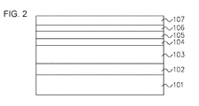
- FIG. 2 is a cross-sectional view schematically illustrating an example of an epitaxial growth process in a process of manufacturing the field effect transistor according to this embodiment.
- FIG. 3 is a cross-sectional view schematically illustrating an example of a process of forming a source electrode and a drain electrode in the process of manufacturing the field effect transistor according to this embodiment.
- FIG. 4 is a cross-sectional view schematically illustrating an example of a process of forming a recess structure in the process of manufacturing the field effect transistor according to this embodiment.
- FIG. 5 is a cross-sectional view schematically illustrating an example of a process of forming a gate insulating film and a gate electrode in the process of manufacturing the field effect transistor according to this embodiment.
- FIG. 6 is a diagram illustrating the distribution of conduction band energy and electron density below the gate electrode in the on and off states of the field effect transistor according to this embodiment.
- FIG. 7 is a characteristic diagram illustrating a variation in a threshold voltage with respect to a change in the thickness of a threshold value control layer in the field effect transistor according to this embodiment.
- FIG. 8 is a diagram schematically illustrating an example of the distribution of conduction band energy and electron density in a region between the source electrode and the gate electrode in the field effect transistor according to this embodiment.
- FIG. 9 is a characteristic diagram illustrating a variation in the connection resistance between a two-dimensional electron gas in the threshold value control layer and a two-dimensional electron gas in a channel layer when the difference between the Al composition of a first electron supply layer and the Al composition of the threshold value control layer is changed in the field effect transistor according to this embodiment.
- FIG. 10 is a characteristic diagram illustrating a variation in the threshold voltage with respect to a change in the thickness of the threshold value control layer in the field effect transistor according to this embodiment.
- FIG. 11 is a characteristic diagram illustrating the rate of change of Vt when the difference between the Al composition of the threshold value control layer and the Al composition of the base layer is changed in the field effect transistor according to this embodiment.
- FIG. 12 is a cross-sectional view illustrating the structure of a normally-off (enhancement) field effect transistor disclosed in Patent Document 1.
- FIG. 13 is a diagram illustrating the distribution of conduction band energy in a region in which a source electrode and a drain electrode are formed in the field effect transistor disclosed in Patent Document 1.
- FIG. 1 is a diagram schematically illustrating an example of the structure of the field effect transistor according to this embodiment.
- a nitride semiconductor applied to the field effect transistor includes a substrate 101 , a buffer layer 102 , a base layer 103 , a channel layer 104 , a first electron supply layer 105 , a threshold value control layer 106 , and a second electron supply layer 107 .
- the base layer 103 is made of Al X Ga 1-X N (0 ⁇ X ⁇ 1) and the channel layer 104 is made of GaN or InGaN.
- the first electron supply layer 105 is an undoped or n-type Al Y Ga 1-Y N layer with a thickness equal to or more than 2 nm and equal to or less than 15 nm.
- the threshold value control layer 106 is an undoped Al Z Ga 1-Z N layer with a thickness equal to or more than 2 nm and equal to or less than 15 nm.
- the second electron supply layer 107 is an undoped or n-type layer.
- the above-mentioned layers are epitaxially grown in this order on the buffer layer formed on the substrate 101 . Therefore, the nitride semiconductor has a laminated structure.
- the Al composition of each of the above-mentioned layers satisfies 0 ⁇ X ⁇ Y ⁇ 1 and 0 ⁇ Z ⁇ Y ⁇ 1.
- the Al composition of each layer may satisfy at least one of Y ⁇ X ⁇ 0.1, Y ⁇ Z ⁇ 0.1, Z ⁇ X ⁇ 0.1, and Y ⁇ W ⁇ 1.
- the field effect transistor includes a source electrode 108 , a drain electrode 109 , and a protective film 110 formed on the surface of the second electron supply layer 107 of the nitride semiconductor.
- the field effect transistor also has a recess structure in which, in a portion of a region between the source electrode 108 and the drain electrode 109 , the entire protective film 110 , the entire second electron supply layer 107 , and a portion of the threshold value control layer 106 are removed by etching.
- the field effect transistor includes a gate electrode 112 that is provided in the recess structure directly or with a gate insulating film 111 interposed therebetween.
- the thickness of the first electron supply layer 105 is equal to or more than 2 nm and equal to or less than 15 nm
- the thickness of the threshold value control layer 106 is equal to or more than 2 nm and equal to or less than 15 nm
- the Al composition of each layer satisfies 0 ⁇ X ⁇ Y ⁇ 1 and 0 ⁇ Z ⁇ Y ⁇ 1. This is based on a variation in the connection resistance between a two-dimensional electron gas in the threshold value control layer 106 and a two-dimensional electron gas in the channel layer 104 and the rate of change of Vt due to a variation in the Al composition of each layer shown in FIGS. 9 and 11 , which will be described below.
- the Al composition of each layer satisfies 0 ⁇ X ⁇ Y ⁇ 1 and 0 ⁇ Z ⁇ Y ⁇ 1, it is possible to obtain the above-mentioned effect of the invention and solve the problems of the invention.
- a threshold voltage shifts closer to a negative side.
- a normally-on type is obtained.
- the thickness of the first electron supply layer 105 is limited to a range of equal to or more than 2 nm and equal to or less than 15 nm and the Al composition of each layer satisfies 0 ⁇ X ⁇ Y ⁇ 1 and Y ⁇ X ⁇ 0.1, a normally-off type can be obtained.
- the rate of change of Vt indicates a variation in threshold voltage (Vt) when the thickness of the threshold value control layer 106 is changed by 1 nm in the field effect transistor according to this embodiment.
- Two-dimensional electron gases 114 and 113 become carriers and a current flows in a given region of the second electron supply layer 107 , which will be described below with reference to FIG. 8 .
- the amount of two-dimensional electron gas increases. Therefore, it is possible to reduce resistance. That is, the Al composition of each layer satisfies Y ⁇ W ⁇ 1 and resistance is reduced.
- a nitride semiconductor applied to a field effect transistor has the following layer structure. That is, a buffer layer 102 , a base layer 103 , a channel layer 104 , a first electron supply layer 105 , a threshold value control layer 106 , and a second electron supply layer 107 are epitaxially grown in this order on a substrate 101 to form the nitride semiconductor.
- the field effect transistor has a source electrode 108 , a drain electrode 109 , and a protective film 110 formed on the surface of the second electron supply layer 107 of the nitride semiconductor.
- the field effect transistor also has a recess structure in which, in a portion of the region between the source electrode 108 and the drain electrode 109 , the entire protective film 110 , the entire second electron supply layer 107 , and a portion of the threshold value control layer 106 are removed by etching.
- the field effect transistor includes a gate electrode 112 that is provided in the recess structure directly or with a gate insulating film 111 interposed therebetween.
- the channel layer 104 is an undoped GaN layer with a thickness of 15 nm.
- the first electron supply layer 105 is an undoped Al 0.15 Ga 0.85 N layer with a thickness of 10 nm.
- the threshold value control layer 106 is an undoped Al 0.07 Ga 0.93 N layer with a thickness of 10 nm.
- the second electron supply layer 107 is an undoped Al 0.25 Ga 0.75 layer with a thickness of 25 nm.
- the Al composition X of the base layer 103 made of Al X Ga 1-X N is 0.07
- the Al composition Y of the first electron supply layer 105 made of Al Y Ga 1-Y N is 0.15
- the Al composition Z of the threshold value control layer 106 made of Al Z Ga 1-Z N is 0.07
- the Al composition W of the second electron supply layer 107 made of Al W Ga 1-W N is 0.25.
- the Al composition of each layer satisfies 0 ⁇ X ⁇ Y ⁇ 1 and 0 ⁇ Z ⁇ Y ⁇ 1.
- the Al composition of each layer also satisfies Y ⁇ X ⁇ 0.1, Y ⁇ Z ⁇ 0.1, Z ⁇ X ⁇ 0.1, and Y ⁇ W ⁇ 1.
- FIGS. 2 to 5 are cross-sectional views schematically illustrating an example of a process of manufacturing the field effect transistor according to this embodiment. Next, an example of a method of manufacturing the field effect transistor according to this embodiment will be described with reference to FIGS. 2 to 5 .
- MOVPE metal organic vapor phase epitaxy
- a Ti/Al (30/180 nm) electrode is formed at a predetermined position on the surface of the second electron supply layer 107 by a vapor deposition/lift-off method using a photoresist mask having an opening pattern in a region in which the source electrode 108 and the drain electrode 109 are formed. Then, rapid thermal annealing (RTA) is performed on the formed Ti/Al (30/180 nm) electrode at 700° C. for 60 seconds to obtain the source electrode 108 and the drain electrode 109 .
- RTA rapid thermal annealing
- the protective film 110 made of SiN is formed with a thickness of 100 nm by a plasma chemical vapor deposition (CVD) method. Then, the protective film 110 is etched by a reactive ion etching (RIE) method using a photoresist mask having an opening pattern at a predetermined position between the source electrode 108 and the drain electrode 109 . After the photoresist mask is removed, the entire second electron supply layer 107 and a portion of the threshold value control layer 106 are removed by an inductively coupled plasma (ICP) dry etching method using the protective film 110 as an etching mask, in a portion of the space between the source electrode 108 and the drain electrode 109 .
- ICP inductively coupled plasma
- the gate insulating film 111 is made of Al 2 O 3 with a thickness of 30 nm by an atomic layer deposition (ALD) method. Then, Ni/Au (30/300 nm) is formed at a predetermined position by a vapor deposition/lift-off method using a photoresist mask having an opening pattern in a region in which the gate electrode 112 is formed, thereby obtaining the gate electrode 112 . Finally, the gate insulating film 111 and the protective film 110 are removed by the reactive ion etching (RIE) method using a photoresist mask having an opening pattern in a region in which the source electrode 108 and the drain electrode 109 are formed. In this way, the field effect transistor is completed.
- RIE reactive ion etching
- FIG. 6 shows a conduction band energy distribution and an electron density distribution in the cross section in a direction vertical to the surface of a wafer, in the vicinity of the center of the region in which the gate electrode 112 is formed in FIG. 1 .
- the conduction band energy is not lower than a Fermi level in the range from the gate insulating film 111 on the surface to the base layer 103 in the conduction band energy distribution. That is, an electron serving as a carrier is not stored in any layer.
- the field effect transistor shown in FIG. 1 when the positive bias voltage Vg is 0 V, the region in which the source electrode 108 is formed and the region in which the drain electrode 109 is formed are electrically isolated from each other below the gate electrode 112 . In this way, the field effect transistor becomes an off state in which no current flows between the source electrode 108 and the drain electrode 109 .
- the two-dimensional electron gas generated in the channel layer 104 electrically connects the region in which the source electrode 108 is formed and the region in which the drain electrode 109 is formed. In this way, the field effect transistor becomes an on state in which a current flows between the source electrode 108 and the drain electrode 109 .
- the field effect transistor according to this embodiment becomes an off state in which no current flows between the source electrode 108 and the drain electrode 109 .
- the field effect transistor according to this embodiment becomes the on state. Therefore, the field effect transistor functions as a normally-off (enhancement) field effect transistor in which a current flows between the source electrode 108 and the drain electrode 109 .
- FIG. 7 shows a variation in the threshold voltage (Vt) when the thickness of the threshold value control layer 106 is changed in the field effect transistor according to this embodiment.
- Vt threshold voltage
- the bottom of the recess structure needs to be formed in the threshold value control layer 106 , and a variation in the etching depth during dry etching is about 3 nm to 4 nm at most. That is, when the thickness of the threshold value control layer 106 is 10 nm as in this embodiment, it is possible to reliably form the bottom of the recess structure in the threshold value control layer 106 .
- FIG. 8 shows the relationship between a conduction band energy distribution and an electron density distribution in the cross section in a direction vertical to the surface of a wafer, in the region between the source electrode 108 and the gate electrode 112 shown in FIG. 1 .
- the conduction band energy is less than the Fermi level in the vicinity of the interface between the second electron supply layer 107 and the threshold value control layer 106 and in the vicinity of the interface between the first electron supply layer 105 and the channel layer 104 .
- An electron serving as a carrier is stored as the two-dimensional electron gas 114 on the side of the threshold value control layer 106 at the interface between the second electron supply layer 107 and the threshold value control layer 106 .
- an electron serving as a carrier is stored as, the two-dimensional electron gas 113 on the side of the channel layer 104 at the interface between the first electron supply layer 105 and the channel layer 104 .
- a two-dimensional electron gas serving as a carrier is stored in two different layers, that is, the threshold value control layer 106 and the channel layer 104 .
- FIG. 9 shows a variation in the connection resistance between the two-dimensional electron gas 114 in the threshold value control layer 106 and the two-dimensional electron gas 113 in the channel layer 104 when the difference (Y ⁇ Z) between the Al composition Y of the first electron supply layer 105 made of Al Y Ga 1-Y N and the Al composition Z of the threshold value control layer 106 made of Al Z Ga 1-Z N is changed in the structure of the field effect transistor according to this embodiment.
- the difference Y ⁇ Z is 0.08.
- the connection resistance between the two-dimensional electron gas 114 in the threshold value control layer 106 and the two-dimensional electron gas 113 in the channel layer 104 is 10 ⁇ 4 ⁇ cm 2 (see reference numeral 201 in FIG. 9 ).
- the connection resistance between the two-dimensional electron gas 114 in the threshold value control layer 106 and the two-dimensional electron gas 113 in the channel layer 104 is 10 0 ⁇ cm 2 (see reference numeral 200 in FIG. 9 ). That is, in the field effect transistor disclosed in Patent Document 1, the connection resistance is four orders of magnitude more than that in the field effect transistor according to this embodiment.
- the Al composition Y of the first electron supply layer 105 and the Al composition Z of the threshold value control layer 106 are considered and the difference between the Al composition Y of the first electron supply layer 105 and the Al composition Z of the threshold value control layer 106 is reduced.
- connection resistance between the two-dimensional electron gas 114 in the threshold value control layer 106 and the two-dimensional electron gas 113 in the channel layer 104 is 10 ⁇ 4 ⁇ cm 2 which is about one order of magnitude more than a connection resistance of 10 ⁇ 5 ⁇ cm 2 between the source and drain electrodes 108 and 109 and the two-dimensional electron gas 114 .
- an example of a structure capable of further reducing the on-resistance will be described below.
- a field effect transistor according to this embodiment is different from that according to the first embodiment in that the threshold value control layer 106 is made of Al 0.15 Ga 0.85 N.
- the Al composition X of the base layer 103 made of Al X Ga 1-X N is 0.07
- the Al composition Y of the first electron supply layer 105 made of Al Y Ga 1-Y N is 0.15
- the Al composition Z of the threshold value control layer 106 made of Al Z Ga 1-Z N is 0.15
- the Al composition W of the second electron supply layer 107 made of Al W Ga 1-W N is 0.25.
- the Al composition of each layer satisfies 0 ⁇ X ⁇ Y ⁇ 1 and 0 ⁇ Z ⁇ Y ⁇ 1.
- each layer satisfies Y ⁇ X ⁇ 0.1, Y ⁇ Z ⁇ 0.1, Z ⁇ X ⁇ 0.1, and Y ⁇ W ⁇ 1.
- a method of manufacturing the field effect transistor according to this embodiment is different from the method of manufacturing the field effect transistor according to the first embodiment described with reference to FIGS. 2 to 5 in that the threshold value control layer 106 may be made of Al 0.15 Ga 0.85 N when the laminated structure of a nitride semiconductor is formed by metal organic vapor phase epitaxy (MOVPE).
- MOVPE metal organic vapor phase epitaxy
- FIG. 9 shows a variation in the connection resistance between the two-dimensional electron gas 114 in the threshold value control layer 106 and the two-dimensional electron gas 113 in the channel layer 104 when the difference (Y ⁇ Z) between the Al composition Y of the first electron supply layer 105 made of Al Y Ga 1-Y N and the Al composition Z of the threshold value control layer 106 made of Al Z Ga 1-Z N is changed in the field effect transistor according to this embodiment.
- the Al composition Y of the first electron supply layer 105 is equal to the Al composition Z of the threshold value control layer 106 , that is, the difference Y ⁇ Z is 0.
- the connection resistance between the two-dimensional electron gas 114 in the threshold value control layer 106 and the two-dimensional electron gas 113 in the channel layer 104 is 10 ⁇ 8 ⁇ cm 2 (see reference numeral 202 in FIG. 9 ).
- This value is three orders of magnitude less than a connection resistance of 10 ⁇ 5 ⁇ cm 2 between the source and drain electrodes 108 and 109 and the two-dimensional electron gas 114 , and the contribution of the value to the on-resistance of the field effect transistor is negligibly small. It is possible to significantly reduce the connection resistance by making the Al composition Y of the first electron supply layer 105 equal to the Al composition Z of the threshold value control layer 106 , that is, by setting the difference Y ⁇ Z to 0.
- the field effect transistor it is possible to significantly reduce the connection resistance between the two-dimensional electron gas 114 in the threshold value control layer 106 and the two-dimensional electron gas 113 in the channel layer 104 . As a result, it is possible to achieve a normally-off field effect transistor with a very low on-resistance.
- FIG. 10 shows a variation in the threshold voltage (Vt) when the thickness of the threshold value control layer 106 is changed in the field effect transistor according to this embodiment.
- FIG. 11 is a characteristic diagram illustrating the rate of change of Vt when the difference (Z ⁇ X) between the Al composition Z of the threshold value control layer 106 and the Al composition X of the base layer 103 is changed.
- the Al composition Z of the threshold value control layer 106 is 0.15 and the Al composition X of the base layer 103 is 0.07. That is, in this embodiment, the difference Z ⁇ X is 0.08.
- the rate of change of Vt is about 58 mV/nm.
- the threshold value controllability of the field effect transistor according to this embodiment is less than that of the field effect transistor according to the first embodiment.
- the field effect transistor according to this embodiment has relatively high threshold value controllability.
- the Al composition Y of the first electron supply layer and the Al composition Z of the threshold value control layer are considered and the difference (Y ⁇ Z) between the Al composition Y of the first electron supply layer and the Al composition Z of the threshold value control layer is reduced.
- the difference (Y ⁇ Z) between the Al composition Y of the first electron supply layer and the Al composition Z of the threshold value control layer is reduced.
- the tradeoff relationship is established between the threshold value controllability and the on-resistance. That is, when the threshold value controllability is improved, the on-resistance increases. When the on-resistance is reduced, the threshold value controllability is reduced.
- the threshold value controllability is reduced.
- a field effect transistor according to this embodiment is different from that according to the first embodiment in that the base layer 103 is made of Al 0.09 Ga 0.91 N and the threshold value control layer 106 is made of Al 0.12 Ga 0.88 N.
- the Al composition X of the base layer 103 made of Al X Ga 1-X N is 0.09
- the Al composition Y of the first electron supply layer 105 made of Al Y Ga 1-Y N is 0.15
- the Al composition Z of the threshold value control layer 106 made of Al Z Ga 1-Z N is 0.12
- the Al composition W of the second electron supply layer 107 made of Al W Ga 1-W N is 0.25.
- the Al composition of each layer satisfies 0 ⁇ X ⁇ Y ⁇ 1 and 0 ⁇ Z ⁇ Y ⁇ 1.
- the Al composition of each layer satisfies Y ⁇ X ⁇ 0.1, Y ⁇ Z ⁇ 0.1, Z ⁇ X ⁇ 0.1, and Y ⁇ W ⁇ 1.
- Y ⁇ Z ⁇ 0.03 and Z ⁇ X ⁇ 0.03 are satisfied.
- the ranges Y ⁇ Z ⁇ 0.03 and Z ⁇ X ⁇ 0.03 are based on the description in FIGS. 9 and 11 .
- a method of manufacturing the field effect transistor according to this embodiment is different from the method of manufacturing the field effect transistor according to the first embodiment shown in FIGS. 2 to 5 in that the base layer 103 is made of Al 0.09 Ga 0.91 N and the threshold value control layer 106 is Al 0.12 Ga 0.88 N when the laminated structure of a nitride semiconductor is obtained by metal organic vapor phase epitaxy (MOVPE).
- MOVPE metal organic vapor phase epitaxy
- FIG. 9 shows a variation in the connection resistance between the two-dimensional electron gas 114 in the threshold value control layer 106 and the two-dimensional electron gas 113 in the channel layer 104 when the difference (Y ⁇ Z) between the Al composition Y of the first electron supply layer 105 made of Al Y Ga 1-Y N and the Al composition Z of the threshold value control layer 106 made of Al Z Ga 1-Z N is changed in the field effect transistor according to this embodiment.
- the Al composition Y of the first electron supply layer 105 is 0.15 and the Al composition Z of the threshold value control layer 106 is 0.12. That is, the difference Y ⁇ Z is 0.03.
- the connection resistance between the two-dimensional electron gas 114 in the threshold value control layer 106 and the two-dimensional electron gas 113 in the channel layer 104 is 10 ⁇ 7 ⁇ cm 2 .
- This value is two orders of magnitude less than a connection resistance of 10 ⁇ 5 ⁇ cm 2 between the source electrode 108 and the drain electrode 109 , and the two-dimensional electron gas 114 , and the contribution of the value to the on-resistance of the field effect transistor is negligibly small.
- connection resistance by reducing the difference (Y ⁇ Z) between the Al composition Y of the first electron supply layer 105 and the Al composition Z of the threshold value control layer 106 , specifically, by reducing the difference Y ⁇ Z to be equal to or less than 0.03.
- the field effect transistor it is possible to reduce the connection resistance between the two-dimensional electron gas 114 in the threshold value control layer 106 and the two-dimensional electron gas 113 in the channel layer 104 . As a result, it is possible to achieve a normally-off field effect transistor with a very small on-resistance.
- FIG. 11 is a characteristic diagram illustrating the rate of change of Vt when the difference (Z ⁇ X) between the Al composition Z of the threshold value control layer 106 and the Al composition X of the base layer 103 is changed.
- the Al composition Z of the threshold value control layer 106 is 0.12 and the Al composition X of the base layer 103 is 0.09. That is, in this embodiment, the difference Z ⁇ X is 0.03.
- the rate of change of Vt is about 21 mV/nm. That is, in this embodiment, it is possible to reduce a variation in the threshold voltage to about one-third of the rate of change of Vt, 58 mV/nm, in the second embodiment. It is possible to reduce the rate of change of Vt by reducing the difference (Z ⁇ X) between the Al composition Z of the threshold value control layer 106 and the Al composition X of the base layer 103 , specifically, by reducing the difference Z ⁇ X to be equal to or less than 0.03.
- the field effect transistor according to this embodiment is a normally-off field effect transistor with very high threshold value controllability.
- the Al composition X of the base layer, the Al composition Y of the first electron supply layer, and the Al composition Z of the threshold value control layer are considered and the differences (Y ⁇ Z) and (Z ⁇ X) are set so as to satisfy Y ⁇ Z ⁇ 0.03 and Z ⁇ X ⁇ 0.03. Therefore, it is possible to achieve a normally-off field effect transistor with both a very small on-resistance and very high threshold value controllability.
- the third embodiment it is possible to improve both a small on-resistance and high threshold value controllability. It is also possible to further improve the on-resistance and the threshold value controllability.
- this embodiment an example of a structure capable of further improving the on-resistance and the threshold value controllability will be described below.
- a field effect transistor according to this embodiment is different from that according to the first embodiment in that, for example, the base layer 103 is made of Al 0.15 Ga 0.85 N and the threshold value control layer 106 is made of Al 0.15 Ga 0.85 N.
- the Al composition X of the base layer 103 made of Al X Ga 1-X N is 0.15
- the Al composition Y of the first electron supply layer 105 made of Al Y Ga 1-Y N is 0.15
- the Al composition Z of the threshold value control layer 106 made of Al Z Ga 1-Z N is 0.15
- the Al composition W of the second electron supply layer 107 made of Al W Ga 1-W N is 0.25.
- the Al composition of each of the above-mentioned layers satisfies 0 ⁇ X ⁇ Y ⁇ 1 and 0 ⁇ Z ⁇ Y ⁇ 1.
- the Al composition of each of the above-mentioned layers satisfies Y ⁇ X ⁇ 0.1, Y ⁇ Z ⁇ 0.1, Z ⁇ X ⁇ 0.1, and Y ⁇ W ⁇ 1.
- a method of manufacturing the field effect transistor according to this embodiment is different from the method of manufacturing the field effect transistor according to the first embodiment shown in FIGS. 2 to 5 in that the base layer 103 is made of Al 0.15 Ga 0.85 N and the threshold value control layer 106 is Al 0.15 Ga 0.85 N when the laminated structure of a nitride semiconductor is obtained by metal organic vapor phase epitaxy (MOVPE).
- MOVPE metal organic vapor phase epitaxy
- FIG. 9 shows a variation in the connection resistance between the two-dimensional electron gas 114 in the threshold value control layer 106 and the two-dimensional electron gas 113 in the channel layer 104 when the difference (Y ⁇ Z) between the Al composition Y of the first electron supply layer 105 made of Al Y Ga 1-Y N and the Al composition Z of the threshold value control layer 106 made of Al Z Ga 1-Z N is changed in the field effect transistor according to this embodiment.
- the Al composition Y of the first electron supply layer 105 is the same as the Al composition Z of the threshold value control layer 106 . That is, in this embodiment, the difference Y ⁇ Z is 0.
- the connection resistance between the two-dimensional electron gas 114 in the threshold value control layer 106 and the two-dimensional electron gas 113 in the channel layer 104 is 10 ⁇ 8 ⁇ cm 2 .
- This value is three orders of magnitude less than a connection resistance of 10 ⁇ 5 ⁇ cm 2 between the source and drain electrodes 108 and 109 and the two-dimensional electron gas 114 , and the contribution of the value to the on-resistance of the field effect transistor is negligibly small. It is possible to significantly reduce the connection resistance by making the Al composition Y of the first electron supply layer 105 equal to the Al composition Z of the threshold value control layer 106 , that is, by setting the difference Y ⁇ Z to 0.
- the field effect transistor it is possible to significantly reduce the connection resistance between the two-dimensional electron gas 114 in the threshold value control layer 106 and the two-dimensional electron gas 113 in the channel layer 104 . As a result, it is possible to achieve a normally-off field effect transistor with a very small on-resistance.
- FIG. 11 is a characteristic diagram illustrating the rate of change of Vt when the difference (Z ⁇ X) between the Al composition Z of the threshold value control layer 106 and the Al composition X of the base layer 103 is changed.
- the Al composition Z of the threshold value control layer 106 is the same as the Al composition X of the base layer 103 . That is, in this embodiment, the difference Z ⁇ X is 0. As can be seen from FIG. 11 , the rate of change of Vt is almost 0 mV/nm. It is possible to significantly reduce the rate of change of Vt by making the Al composition Z of the threshold value control layer 106 equal to the Al composition X of the base layer 103 , that is, by setting the difference Z ⁇ X to 0. As such, the field effect transistor according to this embodiment is a normally-off field effect transistor with very high threshold value controllability.
- the Al composition X of the base layer, the Al composition Y of the first electron supply layer, and the Al composition Z of the threshold value control layer are considered and the Al compositions X, Y, and Z are equal to one another. Therefore, it is possible to achieve a normally-off field effect transistor with both a very small on-resistance and very high threshold value controllability.
- the substrate 101 is not limited to the SiC substrate, but any substrate may be used as long as it can epitaxially grow a nitride-based semiconductor.
- a sapphire substrate, a GaN substrate, a Si substrate, or a SOI substrate may be used.
- the gate insulating film 111 is not limited to the Al 2 O 3 film, but a SiO 2 film, a SiN film, a SiON film, an AlN film, a MgO film, a Sc 2 O 3 film, a ZrO 2 film, a HfO 2 film, or a laminated structure of these films may be used as the gate insulating film 111 .
- a Schottky junction gate in which the gate insulating film 111 is removed and the gate electrode 112 is directly formed in the recess structure may be used.
- the base layer, the channel layer, the first electron supply layer, the threshold value control layer, and the second electron supply layer satisfying at least 0 ⁇ X ⁇ Y ⁇ 1 and 0 ⁇ Z ⁇ Y ⁇ 1 may be laminated in this order.
- the laminated structure of the nitride semiconductor may satisfy at least one of Y ⁇ X ⁇ 0.1, Y ⁇ Z ⁇ 0.1, Z ⁇ X ⁇ 0.1, and Y ⁇ W ⁇ 1.
- the laminated structure of the nitride semiconductor may further include a cap layer.
- a cap layer made of a nitride-based semiconductor is provided on the second electron supply layer, it is possible to stabilize the surface and reduce gate leakage and contact resistance. As such, it is possible to combine various kinds of layers without damaging the effect of the invention.
- the channel layer is made of GaN
- the first electron supply layer is made of Al 0.15 Ga 0.85 N
- the second electron supply layer is made of Al 0.25 Ga 0.75 N.
- the materials and Al compositions of these layers are limited to the above.
- the channel layer may be made of InGaN and the Al compositions of the first and second electron supply layers may be different from those according to the above-described embodiments.
- the thickness of each layer is not limited to that described in the above-described embodiments, but n-type or p-type impurities may be implanted into an appropriate layer or a portion of the layer.
- the value (Y ⁇ Z) is sufficiently small. That is, since the difference between the Al composition of the first electron supply layer and the Al composition of the threshold value control layer is a small value of 0.1 or less, an energy barrier generated by a negative polarized charge and a discontinuous conduction band at the interface between the layers is reduced. Therefore, it is possible to reduce the connection resistance between the two-dimensional electron gas in the threshold value control layer and the two-dimensional electron gas in the channel layer. As a result, it is possible to reduce the on-resistance of a normally-off field effect transistor and thus reduce power consumption.
- the value (Z ⁇ X) is sufficiently small. That is, since the difference between the Al composition of the base layer and the Al composition of the threshold value control layer is a small value of 0.1 or less, it is possible to reduce the rate of change of the threshold voltage (Vt) with respect to the thickness of the threshold value control layer to be equal to or less than several tens of mV/nm.
- the layers forming the laminated structure of the nitride semiconductor are made of different materials.
- the base layer and the threshold value control layer are made of AlGaN and the channel layer is made of GaN or InGaN. Therefore, as described above, in order to reduce the on-resistance and improve threshold value controllability, the difference Y ⁇ Z or Z ⁇ X is reduced, that is, the Al compositions of the base layer and the threshold value control layer increase to be close to the Al composition of the first electron supply layer.
- the channel layer is made of GaN or InGaN with high mobility, it is possible to prevent an increase in channel resistance. Therefore, in a normally-off field effect transistor, it is possible to reduce the on-resistance and improve the threshold value controllability.
- FIGS. 6 to 11 show computer simulation results.
- a symbol “o” or “ ⁇ ” indicates a corresponding point in the first to fourth embodiments or Patent Document 1, that is, a representative point.
- the symbol is not limited to the point.
- the normally-off (enhancement) field effect transistor using the nitride semiconductor according to the invention has a structure that has a low on-resistance and is capable of reducing power consumption. Therefore, the normally-off field effect transistor can be applied to a transistor of a high-power microwave amplifier used in, for example, a base station of a mobile telephone terminal or a satellite communication system, or a transistor used in a power supply of a personal computer (PC) or a power control device of a power steering system of a vehicle, using the above-mentioned advantage.
- PC personal computer
Abstract
Description
d1≦16.4×(1−1.27×(Y−X))/(Y−X)[Å] [Expression 1]
- [Patent Document 1] Japanese Unexamined Patent Publication No. 2008-103617
Claims (10)
Applications Claiming Priority (3)
| Application Number | Priority Date | Filing Date | Title |
|---|---|---|---|
| JP2009-032715 | 2009-02-16 | ||
| JP2009032715 | 2009-02-16 | ||
| PCT/JP2010/000651 WO2010092768A1 (en) | 2009-02-16 | 2010-02-03 | Field effect transistor |
Publications (2)
| Publication Number | Publication Date |
|---|---|
| US20110291160A1 US20110291160A1 (en) | 2011-12-01 |
| US8618578B2 true US8618578B2 (en) | 2013-12-31 |
Family
ID=42561617
Family Applications (1)
| Application Number | Title | Priority Date | Filing Date |
|---|---|---|---|
| US13/147,676 Active 2030-09-11 US8618578B2 (en) | 2009-02-16 | 2010-02-03 | Field effect transistor |
Country Status (3)
| Country | Link |
|---|---|
| US (1) | US8618578B2 (en) |
| JP (1) | JP5697456B2 (en) |
| WO (1) | WO2010092768A1 (en) |
Cited By (2)
| Publication number | Priority date | Publication date | Assignee | Title |
|---|---|---|---|---|
| US9337325B2 (en) | 2011-09-16 | 2016-05-10 | Renesas Electronics Corporation | Semiconductor device and method for manufacturing the same |
| US20200027872A1 (en) * | 2018-07-19 | 2020-01-23 | Macom Technology Solutions Holdings, Inc. | Iii-nitride material semiconductor structures on conductive silicon substrates |
Families Citing this family (15)
| Publication number | Priority date | Publication date | Assignee | Title |
|---|---|---|---|---|
| JP5680987B2 (en) * | 2011-02-18 | 2015-03-04 | 株式会社アドバンテスト | Semiconductor device, test apparatus, and manufacturing method |
| WO2013084020A1 (en) * | 2011-12-09 | 2013-06-13 | Freescale Semiconductor, Inc. | Normally-off high electron mobility transistor and integrated circuit |
| JP6042415B2 (en) * | 2012-04-05 | 2016-12-14 | 東京エレクトロン株式会社 | Manufacturing method of semiconductor device |
| JP2014029990A (en) * | 2012-06-29 | 2014-02-13 | Sharp Corp | Electrode structure of nitride semiconductor device and manufacturing method of the same, and nitride semiconductor field effect transistor |
| TWI506788B (en) * | 2012-12-25 | 2015-11-01 | Huga Optotech Inc | Field effect transistor |
| EP3285302B1 (en) * | 2013-02-15 | 2019-09-11 | AZUR SPACE Solar Power GmbH | Layer structure for a group-iii-nitride normally-off transistor |
| CN103219239B (en) * | 2013-03-27 | 2015-05-27 | 中国电子科技集团公司第五十五研究所 | Method for manufacturing AlGaN/GaN HEMT (High Electron Mobility Transistor) with high thermal stability |
| JP6214978B2 (en) | 2013-09-17 | 2017-10-18 | 株式会社東芝 | Semiconductor device |
| CN103500763B (en) * | 2013-10-15 | 2017-03-15 | 苏州晶湛半导体有限公司 | III nitride semiconductor devices and its manufacture method |
| JP6169958B2 (en) * | 2013-12-02 | 2017-07-26 | 日本電信電話株式会社 | Field effect transistor |
| CN103745922A (en) * | 2013-12-09 | 2014-04-23 | 中国电子科技集团公司第五十五研究所 | Method for manufacturing GaN high electron mobility transistor composite medium insulated gate |
| WO2015166572A1 (en) * | 2014-05-01 | 2015-11-05 | ルネサスエレクトロニクス株式会社 | Semiconductor device and semiconductor device manufacturing method |
| DE112016005025T5 (en) * | 2015-11-02 | 2018-08-23 | Ngk Insulators, Ltd. | EPITAXIAL SUBSTRATE FOR SEMICONDUCTOR ELEMENTS, SEMICONDUCTOR ELEMENTS AND PRODUCTION PROCESS FOR EPITAXIAL SUBSTRATES FOR SEMICONDUCTOR ELEMENTS |
| US10644142B2 (en) * | 2017-12-22 | 2020-05-05 | Nxp Usa, Inc. | Semiconductor devices with doped regions functioning as enhanced resistivity regions or diffusion barriers, and methods of fabrication therefor |
| JP7038765B2 (en) * | 2020-07-22 | 2022-03-18 | ローム株式会社 | Nitride semiconductor equipment |
Citations (7)
| Publication number | Priority date | Publication date | Assignee | Title |
|---|---|---|---|---|
| US6166404A (en) * | 1998-12-28 | 2000-12-26 | Sony Corporation | Semiconductor device in which at least two field effect transistors having different threshold voltages are formed on a common base |
| JP2001085670A (en) | 1999-09-14 | 2001-03-30 | Nec Corp | Field effect type transistor and its manufacturing method |
| JP2006032911A (en) | 2004-06-15 | 2006-02-02 | Ngk Insulators Ltd | Semiconductor laminated structure, semiconductor device, and hemt element |
| JP2007067240A (en) | 2005-08-31 | 2007-03-15 | Toshiba Corp | Nitride semiconductor device |
| WO2007077666A1 (en) | 2005-12-28 | 2007-07-12 | Nec Corporation | Field effect transistor, and multilayered epitaxial film for use in preparation of field effect transistor |
| US20080093626A1 (en) * | 2006-10-20 | 2008-04-24 | Kabushiki Kaisha Toshiba | Nitride semiconductor device |
| US8198652B2 (en) * | 2006-03-29 | 2012-06-12 | Nec Corporation | Field effect transistor with reduced gate leakage current |
Family Cites Families (2)
| Publication number | Priority date | Publication date | Assignee | Title |
|---|---|---|---|---|
| WO2003050849A2 (en) * | 2001-12-06 | 2003-06-19 | Hrl Laboratories, Llc | High power-low noise microwave gan heterojunction field effet transistor |
| CN101604704B (en) * | 2008-06-13 | 2012-09-05 | 西安能讯微电子有限公司 | HEMT device and manufacturing method thereof |
-
2010
- 2010-02-03 JP JP2010550438A patent/JP5697456B2/en active Active
- 2010-02-03 WO PCT/JP2010/000651 patent/WO2010092768A1/en active Application Filing
- 2010-02-03 US US13/147,676 patent/US8618578B2/en active Active
Patent Citations (9)
| Publication number | Priority date | Publication date | Assignee | Title |
|---|---|---|---|---|
| US6166404A (en) * | 1998-12-28 | 2000-12-26 | Sony Corporation | Semiconductor device in which at least two field effect transistors having different threshold voltages are formed on a common base |
| JP2001085670A (en) | 1999-09-14 | 2001-03-30 | Nec Corp | Field effect type transistor and its manufacturing method |
| JP2006032911A (en) | 2004-06-15 | 2006-02-02 | Ngk Insulators Ltd | Semiconductor laminated structure, semiconductor device, and hemt element |
| US7199408B2 (en) * | 2004-06-15 | 2007-04-03 | Ngk Insulators, Ltd. | Semiconductor multilayer structure, semiconductor device and HEMT device |
| JP2007067240A (en) | 2005-08-31 | 2007-03-15 | Toshiba Corp | Nitride semiconductor device |
| WO2007077666A1 (en) | 2005-12-28 | 2007-07-12 | Nec Corporation | Field effect transistor, and multilayered epitaxial film for use in preparation of field effect transistor |
| US8198652B2 (en) * | 2006-03-29 | 2012-06-12 | Nec Corporation | Field effect transistor with reduced gate leakage current |
| US20080093626A1 (en) * | 2006-10-20 | 2008-04-24 | Kabushiki Kaisha Toshiba | Nitride semiconductor device |
| JP2008103617A (en) | 2006-10-20 | 2008-05-01 | Toshiba Corp | Nitride semiconductor device |
Non-Patent Citations (1)
| Title |
|---|
| International Search Report for PCT/JP2010/00065 mailed Apr. 20, 2010. |
Cited By (4)
| Publication number | Priority date | Publication date | Assignee | Title |
|---|---|---|---|---|
| US9337325B2 (en) | 2011-09-16 | 2016-05-10 | Renesas Electronics Corporation | Semiconductor device and method for manufacturing the same |
| US20200027872A1 (en) * | 2018-07-19 | 2020-01-23 | Macom Technology Solutions Holdings, Inc. | Iii-nitride material semiconductor structures on conductive silicon substrates |
| US11038023B2 (en) * | 2018-07-19 | 2021-06-15 | Macom Technology Solutions Holdings, Inc. | III-nitride material semiconductor structures on conductive silicon substrates |
| US11942518B2 (en) | 2018-07-19 | 2024-03-26 | Macom Technology Solutions Holdings, Inc. | Reduced interfacial area III-nitride material semiconductor structures |
Also Published As
| Publication number | Publication date |
|---|---|
| US20110291160A1 (en) | 2011-12-01 |
| WO2010092768A1 (en) | 2010-08-19 |
| JPWO2010092768A1 (en) | 2012-08-16 |
| JP5697456B2 (en) | 2015-04-08 |
Similar Documents
| Publication | Publication Date | Title |
|---|---|---|
| US8618578B2 (en) | Field effect transistor | |
| US8441035B2 (en) | Field effect transistor and method of manufacturing the same | |
| JP5383652B2 (en) | Field effect transistor and manufacturing method thereof | |
| JP5064824B2 (en) | Semiconductor element | |
| US8569797B2 (en) | Field effect transistor and method of manufacturing the same | |
| US7956383B2 (en) | Field effect transistor | |
| CN108028273B (en) | Semiconductor device and method for manufacturing semiconductor device | |
| JP6056435B2 (en) | Semiconductor device | |
| US9171946B2 (en) | Nitride semiconductor device and method of manufacturing the same | |
| JP5587564B2 (en) | Field effect transistor and method of manufacturing field effect transistor | |
| US20130161641A1 (en) | Transistor with enhanced channel charge inducing material layer and threshold voltage control | |
| US20140252371A1 (en) | Heterojunction transistor and method of fabricating the same | |
| KR20100015747A (en) | Cascode circuit employing a depletion-mode, gan-based fet | |
| JP2008010803A (en) | Nitride semiconductor field-effect transistor | |
| US20100148184A1 (en) | Gan-based field effect transistor | |
| CN102856374B (en) | GaN enhanced MIS-HFET device and preparation method of same | |
| JP4474292B2 (en) | Semiconductor device | |
| JP5546104B2 (en) | GaN-based field effect transistor | |
| US10128363B2 (en) | Field effect transistor | |
| CN106531789A (en) | Method for achieving enhanced HEMT through polarity control and enhanced HEMT | |
| JP4748501B2 (en) | High electron mobility transistor | |
| KR20110058332A (en) | Enhancement nitride based semiconductor device employing floating gate structure | |
| JP2010287594A (en) | Field effect transistor | |
| JP2010153748A (en) | Method of manufacturing field effect semiconductor device | |
| JP5655333B2 (en) | Semiconductor structure and manufacturing method thereof |
Legal Events
| Date | Code | Title | Description |
|---|---|---|---|
| AS | Assignment |
Owner name: NEC CORPORATION, JAPAN Free format text: ASSIGNMENT OF ASSIGNORS INTEREST;ASSIGNORS:OTA, KAZUKI;OKAMOTO, YASUHIRO;MIYAMOTO, HIRONOBU;REEL/FRAME:026713/0301 Effective date: 20110728 |
|
| AS | Assignment |
Owner name: RENESAS ELECTRONICS CORPORATION, JAPAN Free format text: ASSIGNMENT OF ASSIGNORS INTEREST;ASSIGNOR:NEC CORPORATION;REEL/FRAME:030811/0968 Effective date: 20130621 |
|
| AS | Assignment |
Owner name: RENESAS ELECTRONICS CORPORATION, JAPAN Free format text: ASSIGNMENT OF ASSIGNORS INTEREST;ASSIGNOR:NEC CORPORATION;REEL/FRAME:030862/0450 Effective date: 20130621 |
|
| STCF | Information on status: patent grant |
Free format text: PATENTED CASE |
|
| FPAY | Fee payment |
Year of fee payment: 4 |
|
| AS | Assignment |
Owner name: RENESAS ELECTRONICS CORPORATION, JAPAN Free format text: CHANGE OF ADDRESS;ASSIGNOR:RENESAS ELECTRONICS CORPORATION;REEL/FRAME:044928/0001 Effective date: 20150806 |
|
| MAFP | Maintenance fee payment |
Free format text: PAYMENT OF MAINTENANCE FEE, 8TH YEAR, LARGE ENTITY (ORIGINAL EVENT CODE: M1552); ENTITY STATUS OF PATENT OWNER: LARGE ENTITY Year of fee payment: 8 |