US10566183B2 - Method of manufacturing semiconductor device and the semiconductor device - Google Patents
Method of manufacturing semiconductor device and the semiconductor device Download PDFInfo
- Publication number
- US10566183B2 US10566183B2 US16/052,929 US201816052929A US10566183B2 US 10566183 B2 US10566183 B2 US 10566183B2 US 201816052929 A US201816052929 A US 201816052929A US 10566183 B2 US10566183 B2 US 10566183B2
- Authority
- US
- United States
- Prior art keywords
- film
- nitride semiconductor
- semiconductor layer
- insulating film
- gate insulating
- Prior art date
- Legal status (The legal status is an assumption and is not a legal conclusion. Google has not performed a legal analysis and makes no representation as to the accuracy of the status listed.)
- Active
Links
- 239000004065 semiconductor Substances 0.000 title claims abstract description 363
- 238000004519 manufacturing process Methods 0.000 title claims abstract description 53
- 150000004767 nitrides Chemical class 0.000 claims abstract description 231
- VYPSYNLAJGMNEJ-UHFFFAOYSA-N Silicium dioxide Chemical compound O=[Si]=O VYPSYNLAJGMNEJ-UHFFFAOYSA-N 0.000 claims abstract description 186
- 238000010438 heat treatment Methods 0.000 claims abstract description 34
- 229910052814 silicon oxide Inorganic materials 0.000 claims description 178
- TWNQGVIAIRXVLR-UHFFFAOYSA-N oxo(oxoalumanyloxy)alumane Chemical compound O=[Al]O[Al]=O TWNQGVIAIRXVLR-UHFFFAOYSA-N 0.000 claims description 172
- 229910052751 metal Inorganic materials 0.000 claims description 54
- 239000002184 metal Substances 0.000 claims description 54
- 238000000034 method Methods 0.000 claims description 54
- PNEYBMLMFCGWSK-UHFFFAOYSA-N aluminium oxide Inorganic materials [O-2].[O-2].[O-2].[Al+3].[Al+3] PNEYBMLMFCGWSK-UHFFFAOYSA-N 0.000 abstract 8
- 229910052593 corundum Inorganic materials 0.000 abstract 8
- 229910001845 yogo sapphire Inorganic materials 0.000 abstract 8
- 229910052681 coesite Inorganic materials 0.000 abstract 4
- 229910052906 cristobalite Inorganic materials 0.000 abstract 4
- 239000000377 silicon dioxide Substances 0.000 abstract 4
- 235000012239 silicon dioxide Nutrition 0.000 abstract 4
- 229910052682 stishovite Inorganic materials 0.000 abstract 4
- 229910052905 tridymite Inorganic materials 0.000 abstract 4
- 239000010408 film Substances 0.000 description 743
- 239000010410 layer Substances 0.000 description 341
- 230000008569 process Effects 0.000 description 40
- 230000015572 biosynthetic process Effects 0.000 description 35
- 229920002120 photoresistant polymer Polymers 0.000 description 32
- 239000000758 substrate Substances 0.000 description 32
- 239000011229 interlayer Substances 0.000 description 19
- JMASRVWKEDWRBT-UHFFFAOYSA-N Gallium nitride Chemical compound [Ga]#N JMASRVWKEDWRBT-UHFFFAOYSA-N 0.000 description 17
- 230000000694 effects Effects 0.000 description 17
- 239000007789 gas Substances 0.000 description 17
- IJGRMHOSHXDMSA-UHFFFAOYSA-N Atomic nitrogen Chemical compound N#N IJGRMHOSHXDMSA-UHFFFAOYSA-N 0.000 description 16
- 229910002704 AlGaN Inorganic materials 0.000 description 15
- 229910002601 GaN Inorganic materials 0.000 description 15
- 230000000052 comparative effect Effects 0.000 description 15
- 238000012545 processing Methods 0.000 description 13
- 238000000151 deposition Methods 0.000 description 12
- 230000008021 deposition Effects 0.000 description 12
- 238000010586 diagram Methods 0.000 description 12
- 229910052710 silicon Inorganic materials 0.000 description 12
- 238000002955 isolation Methods 0.000 description 11
- XUIMIQQOPSSXEZ-UHFFFAOYSA-N Silicon Chemical compound [Si] XUIMIQQOPSSXEZ-UHFFFAOYSA-N 0.000 description 10
- 230000004888 barrier function Effects 0.000 description 10
- 238000001312 dry etching Methods 0.000 description 10
- 229910052757 nitrogen Inorganic materials 0.000 description 10
- 230000001681 protective effect Effects 0.000 description 10
- 239000010703 silicon Substances 0.000 description 10
- 229910052581 Si3N4 Inorganic materials 0.000 description 9
- HQVNEWCFYHHQES-UHFFFAOYSA-N silicon nitride Chemical compound N12[Si]34N5[Si]62N3[Si]51N64 HQVNEWCFYHHQES-UHFFFAOYSA-N 0.000 description 9
- 230000008878 coupling Effects 0.000 description 8
- 238000010168 coupling process Methods 0.000 description 8
- 238000005859 coupling reaction Methods 0.000 description 8
- 238000005530 etching Methods 0.000 description 8
- 238000004518 low pressure chemical vapour deposition Methods 0.000 description 8
- 230000006911 nucleation Effects 0.000 description 8
- 238000010899 nucleation Methods 0.000 description 8
- NRTOMJZYCJJWKI-UHFFFAOYSA-N Titanium nitride Chemical compound [Ti]#N NRTOMJZYCJJWKI-UHFFFAOYSA-N 0.000 description 7
- 238000000231 atomic layer deposition Methods 0.000 description 7
- 239000000470 constituent Substances 0.000 description 7
- 238000011835 investigation Methods 0.000 description 7
- 238000004544 sputter deposition Methods 0.000 description 7
- 229910052796 boron Inorganic materials 0.000 description 6
- 238000005229 chemical vapour deposition Methods 0.000 description 6
- 230000005684 electric field Effects 0.000 description 6
- 239000011261 inert gas Substances 0.000 description 6
- 239000000463 material Substances 0.000 description 6
- 238000000206 photolithography Methods 0.000 description 6
- PIGFYZPCRLYGLF-UHFFFAOYSA-N Aluminum nitride Chemical compound [Al]#N PIGFYZPCRLYGLF-UHFFFAOYSA-N 0.000 description 5
- 229910052782 aluminium Inorganic materials 0.000 description 5
- 238000002425 crystallisation Methods 0.000 description 5
- 230000008025 crystallization Effects 0.000 description 5
- 229920001721 polyimide Polymers 0.000 description 5
- 239000010936 titanium Substances 0.000 description 5
- 230000005533 two-dimensional electron gas Effects 0.000 description 5
- QGZKDVFQNNGYKY-UHFFFAOYSA-N Ammonia Chemical compound N QGZKDVFQNNGYKY-UHFFFAOYSA-N 0.000 description 4
- ZAMOUSCENKQFHK-UHFFFAOYSA-N Chlorine atom Chemical compound [Cl] ZAMOUSCENKQFHK-UHFFFAOYSA-N 0.000 description 4
- KRHYYFGTRYWZRS-UHFFFAOYSA-N Fluorane Chemical compound F KRHYYFGTRYWZRS-UHFFFAOYSA-N 0.000 description 4
- YCKRFDGAMUMZLT-UHFFFAOYSA-N Fluorine atom Chemical compound [F] YCKRFDGAMUMZLT-UHFFFAOYSA-N 0.000 description 4
- 239000000460 chlorine Substances 0.000 description 4
- 229910052801 chlorine Inorganic materials 0.000 description 4
- 150000001875 compounds Chemical class 0.000 description 4
- 230000009647 facial growth Effects 0.000 description 4
- 229910052731 fluorine Inorganic materials 0.000 description 4
- 239000011737 fluorine Substances 0.000 description 4
- 230000012010 growth Effects 0.000 description 4
- XCZXGTMEAKBVPV-UHFFFAOYSA-N trimethylgallium Chemical compound C[Ga](C)C XCZXGTMEAKBVPV-UHFFFAOYSA-N 0.000 description 4
- -1 boron ions Chemical class 0.000 description 3
- 229910052733 gallium Inorganic materials 0.000 description 3
- 238000002513 implantation Methods 0.000 description 3
- 229910044991 metal oxide Inorganic materials 0.000 description 3
- ZOXJGFHDIHLPTG-UHFFFAOYSA-N Boron Chemical compound [B] ZOXJGFHDIHLPTG-UHFFFAOYSA-N 0.000 description 2
- BOTDANWDWHJENH-UHFFFAOYSA-N Tetraethyl orthosilicate Chemical compound CCO[Si](OCC)(OCC)OCC BOTDANWDWHJENH-UHFFFAOYSA-N 0.000 description 2
- XAGFODPZIPBFFR-UHFFFAOYSA-N aluminium Chemical compound [Al] XAGFODPZIPBFFR-UHFFFAOYSA-N 0.000 description 2
- 229910021529 ammonia Inorganic materials 0.000 description 2
- 238000004458 analytical method Methods 0.000 description 2
- PMHQVHHXPFUNSP-UHFFFAOYSA-M copper(1+);methylsulfanylmethane;bromide Chemical compound Br[Cu].CSC PMHQVHHXPFUNSP-UHFFFAOYSA-M 0.000 description 2
- 238000013461 design Methods 0.000 description 2
- 230000005669 field effect Effects 0.000 description 2
- 239000012535 impurity Substances 0.000 description 2
- 150000002500 ions Chemical class 0.000 description 2
- 150000002739 metals Chemical class 0.000 description 2
- 230000004048 modification Effects 0.000 description 2
- 238000012986 modification Methods 0.000 description 2
- 238000005268 plasma chemical vapour deposition Methods 0.000 description 2
- 229910052594 sapphire Inorganic materials 0.000 description 2
- 239000010980 sapphire Substances 0.000 description 2
- 239000002356 single layer Substances 0.000 description 2
- JLTRXTDYQLMHGR-UHFFFAOYSA-N trimethylaluminium Chemical compound C[Al](C)C JLTRXTDYQLMHGR-UHFFFAOYSA-N 0.000 description 2
- 229910016920 AlzGa1−z Inorganic materials 0.000 description 1
- GYHNNYVSQQEPJS-UHFFFAOYSA-N Gallium Chemical compound [Ga] GYHNNYVSQQEPJS-UHFFFAOYSA-N 0.000 description 1
- 229910001218 Gallium arsenide Inorganic materials 0.000 description 1
- 101000831940 Homo sapiens Stathmin Proteins 0.000 description 1
- 102100024237 Stathmin Human genes 0.000 description 1
- 230000004075 alteration Effects 0.000 description 1
- QVGXLLKOCUKJST-UHFFFAOYSA-N atomic oxygen Chemical compound [O] QVGXLLKOCUKJST-UHFFFAOYSA-N 0.000 description 1
- 239000012159 carrier gas Substances 0.000 description 1
- 230000008859 change Effects 0.000 description 1
- 238000000576 coating method Methods 0.000 description 1
- 239000002019 doping agent Substances 0.000 description 1
- 238000005516 engineering process Methods 0.000 description 1
- 229910052737 gold Inorganic materials 0.000 description 1
- 230000006872 improvement Effects 0.000 description 1
- 238000009413 insulation Methods 0.000 description 1
- 238000005468 ion implantation Methods 0.000 description 1
- 150000004706 metal oxides Chemical class 0.000 description 1
- 229910052759 nickel Inorganic materials 0.000 description 1
- 229910052760 oxygen Inorganic materials 0.000 description 1
- 239000001301 oxygen Substances 0.000 description 1
- 238000002161 passivation Methods 0.000 description 1
- 229910052697 platinum Inorganic materials 0.000 description 1
- 229910021420 polycrystalline silicon Inorganic materials 0.000 description 1
- 238000005381 potential energy Methods 0.000 description 1
- 239000002994 raw material Substances 0.000 description 1
- 230000009467 reduction Effects 0.000 description 1
- 238000012827 research and development Methods 0.000 description 1
- 239000007787 solid Substances 0.000 description 1
- 230000001629 suppression Effects 0.000 description 1
- 239000010409 thin film Substances 0.000 description 1
- 229910052719 titanium Inorganic materials 0.000 description 1
- 238000001039 wet etching Methods 0.000 description 1
Images


Classifications
-
- H—ELECTRICITY
- H01—ELECTRIC ELEMENTS
- H01L—SEMICONDUCTOR DEVICES NOT COVERED BY CLASS H10
- H01L21/00—Processes or apparatus adapted for the manufacture or treatment of semiconductor or solid state devices or of parts thereof
- H01L21/02—Manufacture or treatment of semiconductor devices or of parts thereof
- H01L21/02104—Forming layers
- H01L21/02107—Forming insulating materials on a substrate
- H01L21/02109—Forming insulating materials on a substrate characterised by the type of layer, e.g. type of material, porous/non-porous, pre-cursors, mixtures or laminates
- H01L21/02112—Forming insulating materials on a substrate characterised by the type of layer, e.g. type of material, porous/non-porous, pre-cursors, mixtures or laminates characterised by the material of the layer
- H01L21/02123—Forming insulating materials on a substrate characterised by the type of layer, e.g. type of material, porous/non-porous, pre-cursors, mixtures or laminates characterised by the material of the layer the material containing silicon
- H01L21/02164—Forming insulating materials on a substrate characterised by the type of layer, e.g. type of material, porous/non-porous, pre-cursors, mixtures or laminates characterised by the material of the layer the material containing silicon the material being a silicon oxide, e.g. SiO2
-
- H—ELECTRICITY
- H01—ELECTRIC ELEMENTS
- H01L—SEMICONDUCTOR DEVICES NOT COVERED BY CLASS H10
- H01L21/00—Processes or apparatus adapted for the manufacture or treatment of semiconductor or solid state devices or of parts thereof
- H01L21/02—Manufacture or treatment of semiconductor devices or of parts thereof
- H01L21/02104—Forming layers
- H01L21/02107—Forming insulating materials on a substrate
- H01L21/02109—Forming insulating materials on a substrate characterised by the type of layer, e.g. type of material, porous/non-porous, pre-cursors, mixtures or laminates
- H01L21/02112—Forming insulating materials on a substrate characterised by the type of layer, e.g. type of material, porous/non-porous, pre-cursors, mixtures or laminates characterised by the material of the layer
- H01L21/02172—Forming insulating materials on a substrate characterised by the type of layer, e.g. type of material, porous/non-porous, pre-cursors, mixtures or laminates characterised by the material of the layer the material containing at least one metal element, e.g. metal oxides, metal nitrides, metal oxynitrides or metal carbides
- H01L21/02175—Forming insulating materials on a substrate characterised by the type of layer, e.g. type of material, porous/non-porous, pre-cursors, mixtures or laminates characterised by the material of the layer the material containing at least one metal element, e.g. metal oxides, metal nitrides, metal oxynitrides or metal carbides characterised by the metal
- H01L21/02178—Forming insulating materials on a substrate characterised by the type of layer, e.g. type of material, porous/non-porous, pre-cursors, mixtures or laminates characterised by the material of the layer the material containing at least one metal element, e.g. metal oxides, metal nitrides, metal oxynitrides or metal carbides characterised by the metal the material containing aluminium, e.g. Al2O3
-
- H—ELECTRICITY
- H01—ELECTRIC ELEMENTS
- H01L—SEMICONDUCTOR DEVICES NOT COVERED BY CLASS H10
- H01L21/00—Processes or apparatus adapted for the manufacture or treatment of semiconductor or solid state devices or of parts thereof
- H01L21/02—Manufacture or treatment of semiconductor devices or of parts thereof
- H01L21/02104—Forming layers
- H01L21/02107—Forming insulating materials on a substrate
- H01L21/02109—Forming insulating materials on a substrate characterised by the type of layer, e.g. type of material, porous/non-porous, pre-cursors, mixtures or laminates
- H01L21/022—Forming insulating materials on a substrate characterised by the type of layer, e.g. type of material, porous/non-porous, pre-cursors, mixtures or laminates the layer being a laminate, i.e. composed of sublayers, e.g. stacks of alternating high-k metal oxides
-
- H—ELECTRICITY
- H01—ELECTRIC ELEMENTS
- H01L—SEMICONDUCTOR DEVICES NOT COVERED BY CLASS H10
- H01L21/00—Processes or apparatus adapted for the manufacture or treatment of semiconductor or solid state devices or of parts thereof
- H01L21/02—Manufacture or treatment of semiconductor devices or of parts thereof
- H01L21/02104—Forming layers
- H01L21/02107—Forming insulating materials on a substrate
- H01L21/02225—Forming insulating materials on a substrate characterised by the process for the formation of the insulating layer
- H01L21/0226—Forming insulating materials on a substrate characterised by the process for the formation of the insulating layer formation by a deposition process
- H01L21/02263—Forming insulating materials on a substrate characterised by the process for the formation of the insulating layer formation by a deposition process deposition from the gas or vapour phase
- H01L21/02271—Forming insulating materials on a substrate characterised by the process for the formation of the insulating layer formation by a deposition process deposition from the gas or vapour phase deposition by decomposition or reaction of gaseous or vapour phase compounds, i.e. chemical vapour deposition
- H01L21/0228—Forming insulating materials on a substrate characterised by the process for the formation of the insulating layer formation by a deposition process deposition from the gas or vapour phase deposition by decomposition or reaction of gaseous or vapour phase compounds, i.e. chemical vapour deposition deposition by cyclic CVD, e.g. ALD, ALE, pulsed CVD
-
- H—ELECTRICITY
- H01—ELECTRIC ELEMENTS
- H01L—SEMICONDUCTOR DEVICES NOT COVERED BY CLASS H10
- H01L21/00—Processes or apparatus adapted for the manufacture or treatment of semiconductor or solid state devices or of parts thereof
- H01L21/02—Manufacture or treatment of semiconductor devices or of parts thereof
- H01L21/02104—Forming layers
- H01L21/02107—Forming insulating materials on a substrate
- H01L21/02296—Forming insulating materials on a substrate characterised by the treatment performed before or after the formation of the layer
- H01L21/02318—Forming insulating materials on a substrate characterised by the treatment performed before or after the formation of the layer post-treatment
- H01L21/02356—Forming insulating materials on a substrate characterised by the treatment performed before or after the formation of the layer post-treatment treatment to change the morphology of the insulating layer, e.g. transformation of an amorphous layer into a crystalline layer
-
- H—ELECTRICITY
- H01—ELECTRIC ELEMENTS
- H01L—SEMICONDUCTOR DEVICES NOT COVERED BY CLASS H10
- H01L29/00—Semiconductor devices adapted for rectifying, amplifying, oscillating or switching, or capacitors or resistors with at least one potential-jump barrier or surface barrier, e.g. PN junction depletion layer or carrier concentration layer; Details of semiconductor bodies or of electrodes thereof ; Multistep manufacturing processes therefor
- H01L29/40—Electrodes ; Multistep manufacturing processes therefor
- H01L29/43—Electrodes ; Multistep manufacturing processes therefor characterised by the materials of which they are formed
- H01L29/49—Metal-insulator-semiconductor electrodes, e.g. gates of MOSFET
- H01L29/51—Insulating materials associated therewith
- H01L29/511—Insulating materials associated therewith with a compositional variation, e.g. multilayer structures
- H01L29/513—Insulating materials associated therewith with a compositional variation, e.g. multilayer structures the variation being perpendicular to the channel plane
-
- H—ELECTRICITY
- H01—ELECTRIC ELEMENTS
- H01L—SEMICONDUCTOR DEVICES NOT COVERED BY CLASS H10
- H01L29/00—Semiconductor devices adapted for rectifying, amplifying, oscillating or switching, or capacitors or resistors with at least one potential-jump barrier or surface barrier, e.g. PN junction depletion layer or carrier concentration layer; Details of semiconductor bodies or of electrodes thereof ; Multistep manufacturing processes therefor
- H01L29/66—Types of semiconductor device ; Multistep manufacturing processes therefor
- H01L29/66007—Multistep manufacturing processes
- H01L29/66075—Multistep manufacturing processes of devices having semiconductor bodies comprising group 14 or group 13/15 materials
- H01L29/66227—Multistep manufacturing processes of devices having semiconductor bodies comprising group 14 or group 13/15 materials the devices being controllable only by the electric current supplied or the electric potential applied, to an electrode which does not carry the current to be rectified, amplified or switched, e.g. three-terminal devices
- H01L29/66409—Unipolar field-effect transistors
- H01L29/66446—Unipolar field-effect transistors with an active layer made of a group 13/15 material, e.g. group 13/15 velocity modulation transistor [VMT], group 13/15 negative resistance FET [NERFET]
- H01L29/66462—Unipolar field-effect transistors with an active layer made of a group 13/15 material, e.g. group 13/15 velocity modulation transistor [VMT], group 13/15 negative resistance FET [NERFET] with a heterojunction interface channel or gate, e.g. HFET, HIGFET, SISFET, HJFET, HEMT
-
- H—ELECTRICITY
- H01—ELECTRIC ELEMENTS
- H01L—SEMICONDUCTOR DEVICES NOT COVERED BY CLASS H10
- H01L29/00—Semiconductor devices adapted for rectifying, amplifying, oscillating or switching, or capacitors or resistors with at least one potential-jump barrier or surface barrier, e.g. PN junction depletion layer or carrier concentration layer; Details of semiconductor bodies or of electrodes thereof ; Multistep manufacturing processes therefor
- H01L29/66—Types of semiconductor device ; Multistep manufacturing processes therefor
- H01L29/68—Types of semiconductor device ; Multistep manufacturing processes therefor controllable by only the electric current supplied, or only the electric potential applied, to an electrode which does not carry the current to be rectified, amplified or switched
- H01L29/76—Unipolar devices, e.g. field effect transistors
- H01L29/772—Field effect transistors
- H01L29/778—Field effect transistors with two-dimensional charge carrier gas channel, e.g. HEMT ; with two-dimensional charge-carrier layer formed at a heterojunction interface
- H01L29/7782—Field effect transistors with two-dimensional charge carrier gas channel, e.g. HEMT ; with two-dimensional charge-carrier layer formed at a heterojunction interface with confinement of carriers by at least two heterojunctions, e.g. DHHEMT, quantum well HEMT, DHMODFET
- H01L29/7783—Field effect transistors with two-dimensional charge carrier gas channel, e.g. HEMT ; with two-dimensional charge-carrier layer formed at a heterojunction interface with confinement of carriers by at least two heterojunctions, e.g. DHHEMT, quantum well HEMT, DHMODFET using III-V semiconductor material
-
- H—ELECTRICITY
- H01—ELECTRIC ELEMENTS
- H01L—SEMICONDUCTOR DEVICES NOT COVERED BY CLASS H10
- H01L29/00—Semiconductor devices adapted for rectifying, amplifying, oscillating or switching, or capacitors or resistors with at least one potential-jump barrier or surface barrier, e.g. PN junction depletion layer or carrier concentration layer; Details of semiconductor bodies or of electrodes thereof ; Multistep manufacturing processes therefor
- H01L29/02—Semiconductor bodies ; Multistep manufacturing processes therefor
- H01L29/12—Semiconductor bodies ; Multistep manufacturing processes therefor characterised by the materials of which they are formed
- H01L29/20—Semiconductor bodies ; Multistep manufacturing processes therefor characterised by the materials of which they are formed including, apart from doping materials or other impurities, only AIIIBV compounds
- H01L29/2003—Nitride compounds
-
- H—ELECTRICITY
- H01—ELECTRIC ELEMENTS
- H01L—SEMICONDUCTOR DEVICES NOT COVERED BY CLASS H10
- H01L29/00—Semiconductor devices adapted for rectifying, amplifying, oscillating or switching, or capacitors or resistors with at least one potential-jump barrier or surface barrier, e.g. PN junction depletion layer or carrier concentration layer; Details of semiconductor bodies or of electrodes thereof ; Multistep manufacturing processes therefor
- H01L29/40—Electrodes ; Multistep manufacturing processes therefor
- H01L29/41—Electrodes ; Multistep manufacturing processes therefor characterised by their shape, relative sizes or dispositions
- H01L29/417—Electrodes ; Multistep manufacturing processes therefor characterised by their shape, relative sizes or dispositions carrying the current to be rectified, amplified or switched
- H01L29/41725—Source or drain electrodes for field effect devices
- H01L29/41758—Source or drain electrodes for field effect devices for lateral devices with structured layout for source or drain region, i.e. the source or drain region having cellular, interdigitated or ring structure or being curved or angular
-
- H—ELECTRICITY
- H01—ELECTRIC ELEMENTS
- H01L—SEMICONDUCTOR DEVICES NOT COVERED BY CLASS H10
- H01L29/00—Semiconductor devices adapted for rectifying, amplifying, oscillating or switching, or capacitors or resistors with at least one potential-jump barrier or surface barrier, e.g. PN junction depletion layer or carrier concentration layer; Details of semiconductor bodies or of electrodes thereof ; Multistep manufacturing processes therefor
- H01L29/40—Electrodes ; Multistep manufacturing processes therefor
- H01L29/41—Electrodes ; Multistep manufacturing processes therefor characterised by their shape, relative sizes or dispositions
- H01L29/423—Electrodes ; Multistep manufacturing processes therefor characterised by their shape, relative sizes or dispositions not carrying the current to be rectified, amplified or switched
- H01L29/42312—Gate electrodes for field effect devices
- H01L29/42316—Gate electrodes for field effect devices for field-effect transistors
- H01L29/4232—Gate electrodes for field effect devices for field-effect transistors with insulated gate
- H01L29/42356—Disposition, e.g. buried gate electrode
- H01L29/4236—Disposition, e.g. buried gate electrode within a trench, e.g. trench gate electrode, groove gate electrode
-
- H—ELECTRICITY
- H01—ELECTRIC ELEMENTS
- H01L—SEMICONDUCTOR DEVICES NOT COVERED BY CLASS H10
- H01L29/00—Semiconductor devices adapted for rectifying, amplifying, oscillating or switching, or capacitors or resistors with at least one potential-jump barrier or surface barrier, e.g. PN junction depletion layer or carrier concentration layer; Details of semiconductor bodies or of electrodes thereof ; Multistep manufacturing processes therefor
- H01L29/40—Electrodes ; Multistep manufacturing processes therefor
- H01L29/41—Electrodes ; Multistep manufacturing processes therefor characterised by their shape, relative sizes or dispositions
- H01L29/423—Electrodes ; Multistep manufacturing processes therefor characterised by their shape, relative sizes or dispositions not carrying the current to be rectified, amplified or switched
- H01L29/42312—Gate electrodes for field effect devices
- H01L29/42316—Gate electrodes for field effect devices for field-effect transistors
- H01L29/4232—Gate electrodes for field effect devices for field-effect transistors with insulated gate
- H01L29/42372—Gate electrodes for field effect devices for field-effect transistors with insulated gate characterised by the conducting layer, e.g. the length, the sectional shape or the lay-out
- H01L29/42376—Gate electrodes for field effect devices for field-effect transistors with insulated gate characterised by the conducting layer, e.g. the length, the sectional shape or the lay-out characterised by the length or the sectional shape
-
- H—ELECTRICITY
- H01—ELECTRIC ELEMENTS
- H01L—SEMICONDUCTOR DEVICES NOT COVERED BY CLASS H10
- H01L29/00—Semiconductor devices adapted for rectifying, amplifying, oscillating or switching, or capacitors or resistors with at least one potential-jump barrier or surface barrier, e.g. PN junction depletion layer or carrier concentration layer; Details of semiconductor bodies or of electrodes thereof ; Multistep manufacturing processes therefor
- H01L29/40—Electrodes ; Multistep manufacturing processes therefor
- H01L29/43—Electrodes ; Multistep manufacturing processes therefor characterised by the materials of which they are formed
- H01L29/432—Heterojunction gate for field effect devices
Definitions
- the present invention relates to a method of manufacturing a semiconductor device and the semiconductor device.
- the invention can be preferably applied to a semiconductor device using a nitride semiconductor.
- GaN-based nitride semiconductor is expected to be used for a transistor in applications of high withstand voltage, high output, and high frequency because of its wide bandgap and high electron mobility compared with Si or GaAs, and has been actively developed in recent years.
- a transistor having normally-off characteristics is useful, and a structure is earnestly investigated so that the transistor has the normally-off characteristics.
- Japanese Patent No. 5684574 discloses a semiconductor device including an under layer, an electron supply layer, a two-dimensional electron gas cancel layer, a first insulating film, and a gate electrode.
- the inventors have engaged in research and development of a semiconductor device using a nitride semiconductor, and have made earnest investigations on improvement in characteristics of the semiconductor device. Specifically, the inventors have made investigations on a structure (mesa-type MOS structure) of the transistor so that the transistor has the normally-off characteristics.
- threshold voltage of the mesa-type MOS structure is low, roughly 0 V, for example; hence, the threshold voltage is desirably increased so that the normally-off characteristics are effectively exhibited.
- the film stack including Al 2 O 3 stacked on SiO 2 is used to increase a threshold voltage as described in the literature “Origin of electric dipoles formed at high-k/SiO 2 interface”.
- the inventors have examined threshold voltage of a nitride semiconductor device using the film stack including Al 2 O 3 stacked on SiO 2 as a gate insulating film. As a result, the threshold voltage has not increased significantly and reproducibly. Through further investigations, the inventors have examined various film stacks as a gate insulating film. As a result, contrary to the case of a silicon device, when a film stack including SiO 2 stacked on Al 2 O 3 is used, an effect of increasing a threshold voltage has been confirmed in some nitride semiconductor devices. Through analysis, it has been found that the effect of increasing the threshold voltage is given in the case where a lower layer, Al 2 O 3 , is crystallized. Furthermore, a relationship between Vt and thickness of the SiO 2 film has revealed that the effect of increasing the threshold voltage is explained by a dipole model.
- the inventors have made earnest investigations on a structure and a manufacturing method of a nitride semiconductor device to secure an effect of further increasing a threshold voltage, and have achieved a semiconductor device that has good normally-off characteristics while suppressing the reduction in threshold voltage.
- a method of manufacturing a semiconductor device includes a step of forming a gate insulating film over a nitride semiconductor layer.
- the step includes steps of forming a crystalline oxide film of a first metal, forming an oxide film of a second metal over the crystalline oxide film of the first metal, and forming an amorphous oxide film of the first metal over the oxide film of the second metal.
- a semiconductor device includes a gate insulating film formed over a nitride semiconductor layer.
- the gate insulating film includes a stack formed by stacking a crystalline oxide film of a first metal, an oxide film of a second metal, a crystalline oxide film of the first metal, and an oxide film of the second metal in order from a bottom side.
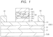
- FIG. 1 is a sectional view illustrating a schematic configuration of a semiconductor device of a first embodiment.
- FIGS. 2A and 2B are each an energy band diagram of the semiconductor device of the first embodiment.
- FIG. 3 is a sectional view illustrating a formation process of a gate insulating film and a gate electrode of the first embodiment.
- FIG. 4 is a sectional view illustrating the formation process of the gate insulating film and the gate electrode of the first embodiment.
- FIG. 5 is a sectional view illustrating the formation process of the gate insulating film and the gate electrode of the first embodiment.
- FIG. 6 is a sectional view illustrating the formation process of the gate insulating film and the gate electrode of the first embodiment.
- FIG. 7 is a sectional view illustrating the formation process of the gate insulating film and the gate electrode of the first embodiment.
- FIG. 8 is a sectional view illustrating the formation process of the gate insulating film and the gate electrode of the first embodiment.
- FIG. 9 is a sectional view illustrating a configuration of a semiconductor device of a first comparative example.
- FIG. 10 is an energy band diagram of the semiconductor device of the first comparative example.
- FIG. 11 is a sectional view illustrating a configuration of a semiconductor device of a second comparative example.
- FIG. 12 is an energy band diagram of the semiconductor device of the second comparative example.
- FIG. 13 is a sectional view illustrating a structure of a semiconductor device using a film stack of a crystalline Al 2 O 3 film and an overlying SiO 2 film as a gate insulating film.
- FIG. 14 is an energy band diagram of the semiconductor device using the film stack of the crystalline Al 2 O 3 film and an overlying SiO 2 film as the gate insulating film.
- FIG. 15 is a sectional view illustrating the configuration of the semiconductor device of the first embodiment.
- FIG. 16 is a plan view illustrating a configuration of the semiconductor device of the first embodiment.
- FIG. 17 is a sectional view illustrating a manufacturing process of the semiconductor device of the first embodiment.
- FIG. 18 is a sectional view illustrating the manufacturing process of the semiconductor device of the first embodiment.
- FIG. 19 is a sectional view illustrating the manufacturing process of the semiconductor device of the first embodiment.
- FIG. 20 is a sectional view illustrating the manufacturing process of the semiconductor device of the first embodiment.
- FIG. 21 is a sectional view illustrating the manufacturing process of the semiconductor device of the first embodiment.
- FIG. 22 is a sectional view illustrating the manufacturing process of the semiconductor device of the first embodiment.
- FIG. 23 is a sectional view illustrating the manufacturing process of the semiconductor device of the first embodiment.
- FIG. 24 is a sectional view illustrating the manufacturing process of the semiconductor device of the first embodiment.
- FIG. 25 is a sectional view illustrating the manufacturing process of the semiconductor device of the first embodiment.
- FIG. 26 is a sectional view illustrating the manufacturing process of the semiconductor device of the first embodiment.
- FIG. 27 is a sectional view illustrating the manufacturing process of the semiconductor device of the first embodiment.
- FIG. 28 is a sectional view illustrating the manufacturing process of the semiconductor device of the first embodiment.
- FIG. 29 is a sectional view illustrating the manufacturing process of the semiconductor device of the first embodiment.
- FIG. 30 is a sectional view illustrating the manufacturing process of the semiconductor device of the first embodiment.
- FIG. 31 is a sectional view illustrating the manufacturing process of the semiconductor device of the first embodiment.
- FIG. 32 is a sectional view illustrating the manufacturing process of the semiconductor device of the first embodiment.
- FIG. 33 is a sectional view illustrating the manufacturing process of the semiconductor device of the first embodiment.
- FIG. 34 is a sectional view illustrating a configuration of a semiconductor device of a second embodiment.
- FIG. 35 is a sectional view illustrating a manufacturing process of the semiconductor device of the second embodiment.
- FIG. 36 is a sectional view illustrating the manufacturing process of the semiconductor device of the second embodiment.
- FIG. 37 is a sectional view illustrating the manufacturing process of the semiconductor device of the second embodiment.
- FIG. 38 is a sectional view illustrating the manufacturing process of the semiconductor device of the second embodiment.
- FIG. 39 is a sectional view illustrating the manufacturing process of the semiconductor device of the second embodiment.
- FIG. 40 is a sectional view illustrating the manufacturing process of the semiconductor device of the second embodiment.
- FIG. 41 is a sectional view illustrating the manufacturing process of the semiconductor device of the second embodiment.
- FIG. 42 is a sectional view illustrating the manufacturing process of the semiconductor device of the second embodiment.
- FIG. 43 is a sectional view illustrating the manufacturing process of the semiconductor device of the second embodiment.
- FIG. 44 is a sectional view illustrating the manufacturing process of the semiconductor device of the second embodiment.
- FIG. 45 is a sectional view illustrating the manufacturing process of the semiconductor device of the second embodiment.
- FIG. 46 is a sectional view illustrating the manufacturing process of the semiconductor device of the second embodiment.
- FIG. 47 is a sectional view illustrating the manufacturing process of the semiconductor device of the second embodiment.
- FIG. 48 is a sectional view illustrating the manufacturing process of the semiconductor device of the second embodiment.
- FIG. 49 is a sectional view illustrating the manufacturing process of the semiconductor device of the second embodiment.
- FIG. 50 is a sectional view illustrating the manufacturing process of the semiconductor device of the second embodiment.
- FIG. 51 is a sectional view illustrating the manufacturing process of the semiconductor device of the second embodiment.
- FIG. 52 is a sectional view illustrating a configuration of a semiconductor device of a first application of a third embodiment.
- FIG. 53 is a sectional view illustrating a configuration of a semiconductor device of a second application of the third embodiment.
- FIG. 54 illustrates a Table of Pauling's electronegativity.
- each of the following embodiments may be dividedly described in a plurality of sections or embodiments for convenience as necessary, they are not unrelated to one another except for the particularly defined case, and are in a relationship where one is a modification, an application, detailed explanation, supplementary explanation, or the like of part or all of another one.
- the number of elements and others including the number, a numerical value, amount, and a range
- the number is not limited to a specified number except for the particularly defined case and for the case where the number is principally clearly limited to the specified number. In other words, the number may be not less than or not more than the specified number.
- a constituent element (including an element step etc.) of the embodiment is not necessarily indispensable except for the particularly defined case and for the case where the constituent element is considered to be indispensable in principle.
- any configuration substantially closely related to or similar to such a shape or the like should be included except for the particularly defined case and for the case where such a configuration is considered to be not included in principle. The same holds true in each of the number of elements and others (including the number, a numerical value, amount, and a range).
- a sectional view for explaining each embodiment may not be hatched for better viewability.
- a plan view may be hatched for better viewability.
- each site does not correspond to size of an actual device, and a particular site may be illustrated to be relatively large for better viewability. Even if a sectional view corresponds to a plan view, a particular site may be illustrated to be relatively large for better viewability.
- FIG. 1 is a sectional view illustrating a schematic configuration of the semiconductor device of the first embodiment.
- the semiconductor device of FIG. 1 is a metal-oxide-semiconductor field effect transistor (MOSFET, MISFET) using a nitride semiconductor.
- MOSFET metal-oxide-semiconductor field effect transistor
- HEMT high electron mobility transistor
- the semiconductor device of FIG. 1 has a structure where a gate electrode is disposed over a mesa part with a gate insulating film in between as described later, and thus may also be referred to as “mesa-type MOS structure”.
- a first nitride semiconductor layer S 1 , a second nitride semiconductor layer S 2 , and a third nitride semiconductor layer S 3 are formed in order over a substrate SUB.
- a mesa part including a fourth nitride semiconductor layer S 4 is formed on a part (substantially the middle in FIG. 1 ) of the third nitride semiconductor layer S 3 .
- the second nitride semiconductor layer S 2 has an electron affinity equal to or larger than that of the first nitride semiconductor layer S 1 (S 1 ⁇ S 2 ).
- the third nitride semiconductor layer S 3 has an electron affinity smaller than that of the first nitride semiconductor layer S 1 (S 1 >S 3 ).
- the fourth nitride semiconductor layer S 4 has an electron affinity larger than that of the first nitride semiconductor layer S 1 (S 4 >S 1 ).
- the first nitride semiconductor layer S 1 which may be referred to as buffer layer, is made of AlGaN, for example.
- the second nitride semiconductor layer S 2 which may be referred to as channel layer, is made of GaN, for example.
- the third nitride semiconductor layer S 3 which may be referred to as barrier layer (electron supply layer), is made of AlGaN, for example.
- the third nitride semiconductor layer S 3 has a larger proportion of Al than the first nitride semiconductor layer S 1 .
- the mesa part including the fourth nitride semiconductor layer S 4 which may be referred to as 2DEG cancel layer (2DEG suppression layer, cap layer), is made of GaN, for example.
- the planar shape of the mesa part including the fourth nitride semiconductor layer S 4 is, for example, a rectangular shape having a long side in a paper depth direction.
- a gate electrode GE is formed over the mesa part including the fourth nitride semiconductor layer S 4 with a gate insulating film GI in between.
- a source electrode SE is formed over the third nitride semiconductor layer S 3 on one side (left side in FIG. 1 ) of the mesa part including the fourth nitride semiconductor layer S 4 , and a drain electrode DE is formed over the third nitride semiconductor layer S 3 on the other side (right side in FIG. 1 ) thereof.
- the planar shape of a stack of the gate electrode GE and the gate insulating film (GI) is a rectangular shape having a long side in the paper depth direction (see FIG. 16 ).
- the planar shape of each of the source electrode SE and the drain electrode DE is also a rectangular shape having a long side in the paper depth direction (see FIG. 16 ).
- the paper depth direction corresponds to a Y direction in FIG. 16 .
- the two-dimensional electron gas (2DEG) is generated in the vicinity of the interface between the second nitride semiconductor layer (channel layer) S 2 and the third nitride semiconductor layer (barrier layer) S 3 and in the second nitride semiconductor layer S 2 .
- the fourth nitride semiconductor layer S 4 has a function of suppressing the 2DEG.
- the function of suppressing the 2DEG may be a function of reducing concentration of the two-dimensional electron gas (2DEG).
- the fourth nitride semiconductor layer S 4 therefore may also be referred to as 2DEG cancel layer.
- a predetermined voltage threshold voltage
- a channel is formed below the gate electrode GE, and a portion between the 2DEG regions becomes conductive by the channel, leading to an on state of the transistor. That is, normally-off operation can be achieved.
- the gate insulating film GI includes a first gate insulating film GIa formed on the mesa part including the fourth nitride semiconductor layer S 4 , a second gate insulating film GIb formed on the first gate insulating film GIa, a third gate insulating film GIc formed on the second gate insulating film GIb, and a fourth gate insulating film GId formed on the third gate insulating film GIc.
- the first gate insulating film GIa and the third gate insulating film GIc are made of crystalline aluminum oxide (c-Al 2 O 3 ).
- the second gate insulating film GIb and the fourth gate insulating film GId are made of silicon oxide (SiO 2 ).
- the first embodiment uses a film stack, which is formed by alternately stacking the crystalline Al 2 O 3 films and the SiO 2 films from the bottom side, as the gate insulating film GI.
- the first embodiment uses a film stack, which is formed by repeatedly stacking the two-layer films including the crystalline Al 2 O 3 films and the overlying SiO 2 films, (uses a film stack of at least two layers) as the gate insulating film GI.
- the above-described compositional ratio between Al, Si, and oxygen (O) is not limitative.
- the film stack which is formed by alternately stacking the crystalline Al 2 O 3 films and the SiO 2 films from the bottom side, is used as the gate insulating film GI; hence, a threshold voltage (Vt) can be shifted in a positive direction. That is, the threshold voltage (Vt) can be increased.
- FIGS. 2A and 2B are each an energy band diagram of the semiconductor device of the first embodiment.
- FIGS. 3 to 8 are each a sectional view illustrating a formation process of the gate insulating film and the gate electrode of the first embodiment.
- FIG. 9 is a sectional view illustrating a structure of a semiconductor device of a first comparative example.
- FIG. 10 is an energy band diagram of the semiconductor device of the first comparative example.
- FIG. 11 is a sectional view illustrating a structure of a semiconductor device of a second comparative example.
- FIG. 12 is an energy band diagram of the semiconductor device of the second comparative example.
- FIG. 13 is a sectional view illustrating a structure of a semiconductor device using a film stack of a crystalline Al 2 O 3 film and an overlying SiO 2 film as a gate insulating film.
- FIG. 14 is an energy band diagram of the semiconductor device using the film stack of the crystalline Al 2 O 3 film and the overlying SiO 2 film as the gate insulating film. The energy band diagram corresponds to the gate electrode, and the gate insulating film and the nitride semiconductor layer below the gate electrode.
- a single-layer amorphous Al 2 O 3 film is used as the gate insulating film GI in the semiconductor device of the first comparative example shown in FIG. 9 .
- a level of a gate electrode GE portion is located below the Fermi level (Ef) as shown by a broken line in FIG. 10 .
- Fermi level Ef
- a direction of an electric field applied to the gate insulating film (a-Al 2 O 3 film) GI is inverted and the threshold voltage (Vt) is reduced due to an interfacial positive charge Q int occurring at an interface between the mesa part including the fourth nitride semiconductor layer S 4 and the gate insulating film (a-Al 2 O 3 film) GI.
- the film stack of the SiO 2 film and the overlying amorphous Al 2 O 3 film provides the effect of increasing the threshold voltage in silicon devices, using such a film stack as the gate insulating film does not increase the threshold voltage in nitride semiconductor devices.
- the energy band is as shown by a thick black solid line in FIG. 12 . That is, since the interfacial positive charge Q int occurring at an interface between the mesa part including the fourth nitride semiconductor layer S 4 and the gate insulating film (a-Al 2 O 3 film) GI is not changed, the direction of the electric field remains inverted.
- SiO 2 has a smaller electron affinity and a lower dielectric constant than Al 2 O 3 , causing a high field strength.
- the threshold voltage (Vt) is further reduced compared with the case of the first comparative example ( FIGS. 9 and 10 ).
- the threshold voltage (Vt) can be increased compared with the case of the second comparative example ( FIGS. 11 and 12 ) as shown in FIG. 14 . In other words, the threshold voltage (Vt) can be shifted in a positive direction.
- Vt threshold voltage
- dipole is formed at a boundary between the crystalline Al 2 O 3 film and the SiO 2 film in the film stack of the crystalline Al 2 O 3 film and the overlying SiO 2 film.
- Such dipole has negative charge ( ⁇ ) on a crystalline Al 2 O 3 film side and positive charge (+) on a SiO 2 film side (see FIG. 14 ).
- a distance between the positive charge and the negative charge is 1 nm or less.
- charge amount charge amount of each of positive charge and negative charge
- charge amount is about one order higher than the amount of the interfacial positive charge Q int , leading to a change in potential energy effective in increasing the threshold voltage.
- the threshold voltage (Vt) can be further increased as shown in FIGS. 2A and 2B .
- the films configuring the gate insulating film GI include a crystalline Al 2 O 3 film (GIa), a SiO 2 film (GIb), a crystalline Al 2 O 3 film (GIc), and a SiO 2 film (GId) in order from the bottom side.
- FIG. 2A shows a band diagram for a stack of two layers of the two-layer film including the crystalline Al 2 O 3 film and the overlying SiO 2 film (four layers in total).
- FIG. 2B shows a band diagram for a stack of three layers of the two-layer film including the crystalline Al 2 O 3 film and the overlying SiO 2 film (six layers in total).
- a level of the gate electrode GE portion is located below the Fermi level (Ef).
- the threshold voltage (Vt) can be increased. Furthermore, when the film stacks including the crystalline Al 2 O 3 films and the SiO 2 films are repeatedly stacked, the amorphous Al 2 O 3 film stacked on the SiO 2 film prevents formation of the reverse dipole that cancels the effect of the dipole. In addition, even if the amorphous Al 2 O 3 film is formed and then crystallized, the reverse dipole is not formed.
- the film stacks including the crystalline Al 2 O 3 films and the SiO 2 films are repeatedly stacked, thereby the threshold voltage is cumulatively increased, so that the threshold voltage (Vt) can be made positive.
- the threshold voltage (Vt) can be easily adjusted.
- the Al 2 O 3 film as the lower layer may be amorphous.
- the Al 2 O 3 film is exposed to the above atmosphere, thereby the SiO 2 film is formed on the Al 2 O 3 film of which at least the surficial portion is concurrently crystallized; hence, the dipole is formed.
- the effect of increasing the threshold voltage by the dipole is now quantitatively described from the viewpoint of charge.
- thickness of the Al 2 O 3 film on the interface, at which the interfacial positive charge Q int of 1 ⁇ 10 12 cm ⁇ 2 exists is assumed to be 60 nm
- the threshold voltage is reduced by 1.2 V.
- the dipole charge occurring at the interface between the crystalline Al 2 O 3 film and the SiO 2 film in the first embodiment is 3.5 ⁇ 10 13 cm ⁇ 2 , which is an order of magnitude greater than the interfacial positive charge Q int , leading to the effect of an increase in the threshold voltage of 0.7 V.
- the effect of an increase in the threshold voltage of 1.4 V is given by stacking the film stacks two times, and an increase of 2.1 V is given by stacking the film stacks three times.
- the film stacks are stacked at least two times, thereby the effect of increasing the threshold voltage is obtained beyond the effect of reducing the threshold voltage by the interfacial positive charge Q int .
- a manufacturing process of the gate insulating film, the gate electrode, and the like of the semiconductor device of the first embodiment is now described with reference to FIGS. 3 to 8 , while a stacking state of the Al 2 O 3 film and the SiO 2 film and formation of the dipole are described.
- a substrate SUB as shown in FIG. 3 is provided, and first to third nitride semiconductor layers (S 1 to S 3 ) are formed in order.
- a semiconductor substrate made of, for example, silicon (Si) is used as the substrate SUB.
- a GaN layer as the second nitride semiconductor layer (channel layer) S 2
- an AlGaN layer (Al proportion 22%) as the third nitride semiconductor layer (barrier layer) S 3 are epitaxially grown in order over the substrate SUB.
- a GaN layer is epitaxially grown as a fourth nitride semiconductor layer S 4 on the third nitride semiconductor layer S 3 , and then an undepicted mask film is formed in a formation region of a mesa part, and the fourth nitride semiconductor layer S 4 is etched with the mask film as a mask. As a result, the mesa part is formed.
- the gate insulating film GI and the gate electrode GE are formed over the mesa part including the fourth nitride semiconductor layer S 4 .
- a crystalline aluminum oxide c-Al 2 O 3
- amorphous aluminum oxide a-Al 2 O 3
- ALD atomic layer deposition
- the amorphous aluminum oxide (a-Al 2 O 3 ) is subjected to heat treatment for 10 min at 800° C. in an inert gas (for example, nitrogen) atmosphere. Through the heat treatment, the amorphous aluminum oxide (a-Al 2 O 3 ) is crystallized and thus formed into the crystalline aluminum oxide (c-Al 2 O 3 ).
- an inert gas for example, nitrogen
- crystallization means treatment to produce grains
- the crystalline aluminum oxide (c-Al 2 O 3 ) has a number of grains.
- the crystalline aluminum oxide may therefore referred to as polycrystalline aluminum oxide.
- the average grain size of the grains is preferably similar ( ⁇ 80%) to the thickness of the aluminum oxide film (a-Al 2 O 3 , c-Al 2 O 3 ).
- the thickness of the aluminum oxide film (a-Al 2 O 3 , c-Al 2 O 3 ) is about 5 nm in this case, the thickness can be adjusted within a range from 2 to 20 nm, more preferably 5 to 10 nm.
- the thickness of 2 nm or more allows dipole formation.
- the thickness is preferably 5 nm or more to secure a sufficiently large dipole (increase the charge amount).
- the thickness has no upper limit, when the two-layer films including the crystalline Al 2 O 3 films and the overlying SiO 2 films are repeatedly stacked, the thickness is sufficiently 20 nm or less.
- the thickness is more preferably 10 nm or less to suppress influence of the interfacial positive charge Q int .
- a silicon oxide film (SiO 2 film) is formed as the second gate insulating film GIb on the first gate insulating film GIa.
- the silicon oxide film (SiO 2 film) is formed at a deposition temperature of 400° C. so as to have a thickness of 10 nm using a low pressure chemical vapor deposition (LPCVD) process.
- LPCVD low pressure chemical vapor deposition
- the thickness of the silicon oxide film (SiO 2 film) is about 10 nm in this case, the thickness can be adjusted within a range from 5 to 20 nm, more preferably 5 to 10 nm. The thickness of 5 nm or more allows dipole formation.
- the thickness has no upper limit, when the two-layer films including the crystalline Al 2 O 3 films and the overlying SiO 2 films are repeatedly stacked, the thickness is sufficiently 20 nm or less.
- the thickness is more preferably nm or less to suppress influence of the interfacial positive charge Q int .
- the silicon oxide film (SiO 2 film) is formed as the second gate insulating film GIb on the crystalline aluminum oxide (c-Al 2 O 3 ); hence, dipole is formed at the interface between such films.
- the crystalline aluminum oxide (c-Al 2 O 3 ) is formed as the third gate insulating film GIc on the second gate insulating film GIb.
- the amorphous aluminum oxide (a-Al 2 O 3 ) is formed at a deposition temperature of 300° C. so as to have a thickness of 10 nm using an ALD process.
- the amorphous aluminum oxide (a-Al 2 O 3 ) film is formed on the silicon oxide film (SiO 2 film) as the second gate insulating film GIb; hence, no dipole is formed at the interface between such films.
- the amorphous aluminum oxide (a-Al 2 O 3 ) is subjected to heat treatment for 10 min at 800° C. in an inert gas (for example, nitrogen) atmosphere.
- an inert gas for example, nitrogen
- the amorphous aluminum oxide (a-Al 2 O 3 ) is crystallized and thus formed into the crystalline aluminum oxide (c-Al 2 O 3 ) ( FIG. 6 ).
- the above heat treatment condition is an exemplary condition. However, heat treatment at 800° C. or higher is preferably performed to crystallize the amorphous aluminum oxide (a-Al 2 O 3 ).
- the thickness of the aluminum oxide film (a-Al 2 O 3 , c-Al 2 O 3 ) to be the third gate insulating film GIc can be adjusted within a range from 2 to 20 nm, more preferably 5 to 10 nm.
- the thickness of 2 nm or more allows dipole formation.
- the thickness is preferably 5 nm or more to secure a sufficiently large dipole (increase the charge amount).
- the thickness has no upper limit, when the two-layer films including the crystalline Al 2 O 3 films and the overlying SiO 2 films are repeatedly stacked, the thickness is sufficiently 20 nm or less.
- the thickness is more preferably 10 nm or less to suppress influence of the interfacial positive charge Q int .
- a silicon oxide film (SiO 2 film) is formed as the fourth gate insulating film GId on the third gate insulating film GIc.
- the silicon oxide film (SiO 2 film) is formed at a deposition temperature of 400° C. so as to have a thickness of 10 nm using a LPCVD process.
- the thickness of the silicon oxide film (SiO 2 film) to be the fourth gate insulating film GId can be adjusted within a range from 5 to 20 nm, more preferably 5 to 10 nm. The thickness of 5 nm or more allows dipole formation.
- the thickness has no upper limit, when the two-layer films including the crystalline Al 2 O 3 film and the overlying SiO 2 film are repeatedly stacked, the thickness is sufficiently 20 nm or less.
- the thickness is more preferably 10 nm or less to suppress influence of the interfacial positive charge Q int .
- the silicon oxide film (SiO 2 film) is formed as the fourth gate insulating film GId on the crystalline aluminum oxide (c-Al 2 O 3 ); hence, dipole is formed at the interface between such films.
- formation of dipole is not simply due to contact of the Al 2 O 3 film and the SiO 2 film, but is due to crystallinity of the Al 2 O 3 film and a stacking order of the films.
- the experimental facts of “dipole is formed by forming the silicon oxide film (SiO 2 film) on the crystalline aluminum oxide (c-Al 2 O 3 )” and “no dipole is formed in the case where the amorphous aluminum oxide (a-Al 2 O 3 ) is formed on the silicon oxide film (SiO 2 film) and crystallized” are used, so that the threshold voltage can be cumulatively increased using the gate insulating film formed by repeatedly stacking the two-layer films including the crystalline Al 2 O 3 films and the overlying SiO 2 films.
- the gate insulating film GI includes four layers (GIa to GId) in this case, the gate insulating film GI may include six, eight, or at least ten layers.
- the films configuring the gate insulating film GI include the crystalline Al 2 O 3 film (GIa) 5 nm thick, the SiO 2 film (GIb) 10 nm thick, the crystalline Al 2 O 3 film (GIc) 10 nm thick, and the SiO 2 film (GId) 10 nm thick from the bottom side.
- GIa crystalline Al 2 O 3 film
- GIb SiO 2 film
- GIc crystalline Al 2 O 3 film
- GId SiO 2 film
- the gate insulating film may include the crystalline Al 2 O 3 film (GIa) 5 nm thick, the SiO 2 film (GIb) 5 nm thick, the crystalline Al 2 O 3 film (GIc) 5 nm thick, the SiO 2 film (GIb) 5 nm thick, the crystalline Al 2 O 3 film (GIc) 5 nm thick, and the SiO 2 film (GId) 10 nm thick, which are stacked in order from the bottom side.
- GIa crystalline Al 2 O 3 film
- GIb SiO 2 film
- GIc crystalline Al 2 O 3 film
- GId SiO 2 film
- a titanium nitride (TiN) film is deposited as a conductive film for the gate electrode GE on the gate insulating film (fourth gate insulating film GId) GI at a thickness of about 100 nm using a sputtering process or the like.
- an undepicted photoresist film is formed in the formation region of the gate electrode GE, and the conductive film for the gate electrode GE and the underlying gate insulating film GI (GIa to GId) are etched with the photoresist film as a mask.
- the gate electrode GE is formed, and the gate insulating film GI (GIa to GId) having the same planar shape as the gate electrode GE is formed under the gate electrode GE (see FIG. 1 ). Subsequently, the photoresist film is removed.
- a source electrode SE and a drain electrode DE are formed.
- the source electrode SE and the drain electrode DE are formed using a liftoff process, for example.
- regions other than the formation regions of the source electrode SE and the drain electrode DE are covered with an undepicted photoresist film, and a conductive film is formed above the substrate SUB.
- an aluminum film is deposited using a sputtering process or the like.
- the photoresist film is removed, and the conductive film in the regions other than the formation regions of the source and drain electrodes SE and DE are removed.
- the semiconductor device of FIG. 1 can be formed.
- the semiconductor device of the first embodiment is further described in detail with reference to FIGS. 15 to 33 .
- FIG. 15 is a sectional view illustrating a configuration of the semiconductor device of the first embodiment.
- FIG. is a plan view illustrating the configuration of the semiconductor device of the first embodiment.
- the sectional view of FIG. 15 corresponds to a portion A-A in FIG. 16 , for example.
- the first nitride semiconductor layer S 1 , the second nitride semiconductor layer S 2 , and the third nitride semiconductor layer S 3 are formed in order over the substrate SUB.
- the mesa part including the fourth nitride semiconductor layer S 4 is formed on a part of the third nitride semiconductor layer S 3 .
- a nucleation layer and an overlying high-resistance buffer layer may be formed over the substrate SUB before formation of the first nitride semiconductor layer S 1 and others.
- a semiconductor substrate made of silicon (Si) exposing a (111) plane may be used as the substrate SUB.
- a SiC or sapphire substrate may be used as the substrate SUB.
- a substrate made of GaN may also be used. In such a case, the nucleation layer may be omitted.
- the nucleation layer includes a nitride semiconductor layer.
- a nitride semiconductor layer For example, an aluminum nitride (AlN) layer can be used as the nucleation layer.
- the high-resistance buffer layer includes one or more nitride semiconductor layers each including a nitride semiconductor doped with an impurity forming a deep level.
- a superlattice structure (superlattice layer) including a plurality of nitride semiconductor layers can be formed by repeatedly stacking film stacks (AlN/GaN film) including gallium nitride (GaN) layers and aluminum nitride (AlN) layers so as to be used as the high-resistance buffer layer.
- any of the nitride semiconductor layers (III-V compound semiconductor layers) over the substrate SUB is typically formed by group III face growth.
- the first nitride semiconductor layer S 1 , the second nitride semiconductor layer S 2 , and the third nitride semiconductor layer S 3 are formed in order over the substrate SUB.
- the mesa part including the fourth nitride semiconductor layer S 4 is formed on a part of the third nitride semiconductor layer S 3 .
- the second nitride semiconductor layer S 2 has an electron affinity equal to or larger than that of the first nitride semiconductor layer S 1 (S 1 ⁇ S 2 ).
- the third nitride semiconductor layer S 3 has an electron affinity smaller than that of the first nitride semiconductor layer S 1 (S 1 >S 3 ).
- the fourth nitride semiconductor layer S 4 has an electron affinity larger than that of the first nitride semiconductor layer S 1 (S 4 >S 1 ).
- the first nitride semiconductor layer S 1 which may be referred to as buffer layer, is made of AlGaN, for example.
- the second nitride semiconductor layer S 2 which may be referred to as channel layer, is made of GaN, for example.
- the third nitride semiconductor layer S 3 which may be referred to as barrier layer (electron supply layer), is made of AlGaN, for example.
- the third nitride semiconductor layer S 3 has a larger Al proportion than the first nitride semiconductor layer S 1 .
- the Al proportion of the first nitride semiconductor layer S 1 is 0 to 10%, more preferably 3 to 8%.
- the Al proportion of the third nitride semiconductor layer S 3 is 15 to 30%, more preferably 18 to 22%.
- the fourth nitride semiconductor layer (2DEG cancel layer) S 4 is an undoped layer, and includes, for example, i-GaN, but may include AlGaN having a smaller Al proportion than the first nitride semiconductor layer S 1 .
- the fourth nitride semiconductor layer S 4 may also include InGaN.
- the gate electrode GE is formed over the mesa part including the fourth nitride semiconductor layer S 4 with the gate insulating film GI in between.
- the planar shape of the mesa part is a rectangular shape having a long side in the paper depth direction.
- a stack of the gate insulating film (GI) and the gate electrode GE has a planar shape being a rectangular shape having a long side in the paper depth direction (Y direction) (see FIG. 16 ).
- the width (length in the X direction, length in the current flow direction from the drain electrode to the source electrode, i.e., in the gate length direction) of the gate electrode GE is larger than the width (length in the X direction) of the mesa part.
- a film including four layers (GIa to GId) is formed as the gate insulating film GI in the first embodiment.
- the gate insulating film including a stack of two layers of two-layer film including the crystalline Al 2 O 3 as the lower layer and the silicon oxide (SiO 2 ) as the upper layer.
- the first embodiment uses film stack, which is formed by repeatedly stacking the two-layer films including the crystalline Al 2 O 3 films and the overlying SiO 2 films, as the gate insulating film GI.
- the Al 2 O 3 film on the SiO 2 film is formed in an amorphous state and then crystallized.
- Such a film stack is used as the gate insulating film GI, thereby the threshold voltage (Vt) can be increased as described above.
- a field plate insulating film FP is formed on the third nitride semiconductor layer S 3 on both sides of the mesa part.
- the field plate insulating film FP having an opening is formed over the third nitride semiconductor layer S 3 , and the mesa part is disposed in the opening.
- the gate insulating film GI and the gate electrode GE are disposed so as to cover the opening of the field plate insulating film FP. Consequently, the width (length in the X direction) of the opening of the field plate insulating film FP is smaller than the width (length in the X direction) of the gate electrode GE, but larger than the width (length in the X direction) of the mesa part. In this way, the field plate insulating film FP is provided below the end portion of the gate electrode GE, making it possible to increase the withstand voltage of the semiconductor device.
- An interlayer insulating film IL 1 is formed over the gate electrode GE.
- the source electrode SE and the drain electrode DE are formed over the third nitride semiconductor layer S 3 on the two respective sides of the mesa part (S 4 ).
- contact holes (coupling holes) C 1 are formed in the interlayer insulating film IL 1 , and the source electrode SE and the drain electrode DE are disposed in and on the respective contact holes C 1 .
- An insulating film IL 2 is formed over the source electrode SE and the drain electrode DE.
- the insulating film IL 2 is a film stack of a lower film IL 2 a and an upper film IL 2 b.
- the planar shape of the drain electrode DE is a rectangular shape having a long side in the Y direction.
- the planar shape of the source electrode SE is also a rectangular shape having a long side in the Y direction.
- a contact hole C 1 to be a coupling part (coupling region) between the drain electrode DE and the third nitride semiconductor layer S 3 is disposed below the drain electrode DE.
- the planar shape of the contact hole C 1 is a rectangular shape having a long side in the Y direction.
- a contact hole C 1 to be a coupling part (coupling region) between the source electrode SE and the third nitride semiconductor layer S 3 is disposed below the source electrode SE.
- the planar shape of the contact hole C 1 is a rectangular shape having a long side in the Y direction.
- the gate electrode GE is disposed between the drain electrode DE and the source electrode SE. As described above, the gate electrode GE has a rectangular shape having the long side in the Y direction.
- drain electrodes DE As shown in FIG. 16 , a plurality of drain electrodes DE, gate electrodes GE, and source electrodes SE are repeatedly disposed.
- the planar shape of the drain electrode DE is the rectangular shape having the long side in the Y direction.
- the plurality of linear drain electrodes DE are arranged in the X direction at a certain interval.
- the planar shape of the source electrode SE is the rectangular shape having the long side in the Y direction.
- the plurality of linear source electrodes SE each have a linear shape, and are arranged in the X direction at a certain interval.
- the source electrodes SE and the drain electrodes DE are alternately arranged along the X direction.
- the gate electrode GE is disposed between the contact hole C 1 below the drain electrode DE and the contact hole C 1 below the source electrode SE.
- the drain electrodes DE are coupled to one another by a drain pad (terminal part) DP.
- the drain pad DP is disposed so as to extend in the X direction on one end side (for example, the upper side in FIG. 16 ) of the drain electrode DE.
- the drain electrodes DE are disposed so as to protrude in the Y direction from the drain pad D 1 extending in the X direction.
- Such a shape may be referred to as comblike shape.
- the source electrodes SE are coupled to one another by a source pad (terminal part) SP.
- the source pad SP is disposed so as to extend in the X direction on one end side (for example, the lower side in FIG. 16 ) of the source electrode SE.
- the source electrodes SE are disposed so as to protrude in the Y direction from the source pad SP extending in the X direction.
- Such a shape may be referred to as comblike shape.
- the gate electrodes GE are coupled to one another by a gate line GL.
- the gate line GL is disposed so as to extend in the X direction on one end side (for example, the lower side in FIG. 16 ) of the gate electrode GE.
- the gate electrodes GE are disposed so as to protrude in the Y direction from the gate line GL extending in the X direction.
- the gate line GL is coupled to a gate pad GP provided on each side (for example, each of right and left sides in FIG. 16 ) in the X direction of the gate line GL.
- the mesa part of the fourth nitride semiconductor layer S 4 is disposed below the gate electrodes GE and the gate line GL with the gate insulating film (GI) in between.
- the source electrodes SE, the drain electrodes DE, and the gate electrodes GE are disposed mainly over an active region AC surrounded by an element isolation region ISO.
- the planar shape of the active region AC is a rectangular shape having a long side in the X direction.
- the drain pad DP, the gate line GL, and the source pad SP are disposed over the element isolation region ISO.
- the gate line GL is disposed between the active region AC and the source pad SP.
- an ion species such as boron (B) or nitrogen (N) is implanted by ion implantation or the like, so that crystallinity of the nitride semiconductor layer is disrupted.
- FIGS. 17 to 33 are each a sectional view illustrating a manufacturing process of the semiconductor device of the first embodiment.
- the substrate SUB is provided, and the first to fourth nitride semiconductor layers (S 1 to S 4 ) are formed in order.
- a semiconductor substrate made of silicon (Si) exposing a (111) plane is used as the substrate SUB.
- a substrate made of SiC or sapphire may be used as the substrate SUB.
- a substrate made of GaN may also be used.
- Any of subsequently formed nitride semiconductor layers (III-V compound semiconductor layers) is typically formed by group III face growth (herein, gallium face growth or aluminum face growth).
- a nucleation layer and a high-resistance buffer layer may be formed on the substrate SUB before the first to fourth nitride semiconductor layers (S 1 to S 4 ) are formed in order.
- an aluminum nitride (AlN) layer can be used as the nucleation layer, which can be formed by epitaxial growth using a metal organic chemical vapor deposition (MOCVD) process, for example.
- a superlattice structure which is formed by repeatedly stacking film stacks (AlN/GaN film) including gallium nitride (GaN) layers and aluminum nitride (AlN) layers, can be used as the high-resistance buffer layer.
- Such a superlattice structure can be formed by alternate epitaxial growth of the gallium nitride (GaN) layer and the aluminum nitride (AlN) layer using the metal organic chemical vapor deposition process, for example.
- an AlGaN layer (Al proportion 5%) is epitaxially grown about 1 ⁇ m as the first nitride semiconductor layer (buffer layer) S 1 over the substrate SUB using a metal organic chemical vapor deposition process or the like.
- the constituent element ratio of the AlGaN layer can be adjusted within a range of X of 0 to 0.1 (0 ⁇ X ⁇ 0.1), more preferably X of 0.03 to 0.08 (0.03 ⁇ X ⁇ 0.08) for Al x Ga 1-x N, for example.
- X is 0.05.
- the AlGaN layer is an undoped layer, for example. That is, the AlGaN layer is not intentionally doped with an n-type or p-type impurity.
- a GaN layer is epitaxially grown about 40 nm as the second nitride semiconductor layer (channel layer) S 2 on the first nitride semiconductor layer S 1 using a metal organic chemical vapor deposition process or the like.
- an AlGaN layer (Al proportion 22%) is epitaxially grown about 14 nm as the third nitride semiconductor layer (barrier layer) S 3 on the second nitride semiconductor layer S 2 using a metal organic chemical vapor deposition process or the like.
- Z is larger than X, 0.15 to less than 0.3 (0.15 ⁇ Z ⁇ 0.3), more preferably 0.18 to 0.22 (0.18 ⁇ Z ⁇ 0.22) for Al z Ga 1-z N, for example.
- the two-dimensional electron gas (2DEG) is generated at the interface between the second nitride semiconductor layer (channel layer) S 2 and the third nitride semiconductor layer (barrier layer) S 3 and in the second nitride semiconductor layer S 2 .
- a GaN layer is epitaxially grown about 25 nm as the fourth nitride semiconductor layer S 4 on the third nitride semiconductor layer S 3 using a metal organic chemical vapor deposition process or the like.
- the 2DEG disappears through such formation of the fourth nitride semiconductor layer S 4 .
- the first to fourth nitride semiconductor layers S 1 to S 4 are each grown while a carrier gas and a source gas are introduced into an apparatus, for example.
- a gas containing constituent elements of the nitride semiconductor layer (herein, AlGaN layer or GaN layer) is used as the source gas.
- AlGaN layer trimethyl aluminum (TMA 1 ), trimethyl gallium (TMG), and ammonia are used as the source gases of Al, Ga, and N, respectively.
- TMG trimethyl gallium
- ammonia are used as the source gases of Ga and N, respectively.
- an element isolation region (ISO), which cannot be shown in the section of FIG. 17 is formed (see FIG. 16 ).
- a protective film such as an insulating film is formed to cover over the fourth nitride semiconductor layer S 4 , and an undepicted photoresist film to open the element isolation region is formed on the protective film by photolithography processing.
- boron ions are implanted through the protective film with the photoresist film as a mask to form the element isolation region (ISO).
- the ion species such as boron (B) or nitrogen (N) is implanted, thereby crystallinity of the nitride semiconductor layer is disrupted, so that the element isolation region (ISO) is formed.
- boron ions are implanted at a density of about 1 ⁇ 10 14 to 4 ⁇ 10 14 cm ⁇ 2 into part of the stack including the first to fourth nitride semiconductor layers S 1 to S 4 .
- the implantation energy is about 100 to 200 keV, for example.
- the implantation condition of the boron ions is adjusted such that the implantation depth, i.e., the bottom of the element isolation region (ISO) is located below the bottom surface of the third nitride semiconductor layer (barrier layer) S 3 , for example. In this way, the element isolation region (ISO) is formed.
- the region surrounded by the element isolation region (ISO) corresponds to the active region AC. As shown in FIG. 16 , the active region AC has a substantially rectangular shape. Subsequently, the photoresist film is removed by plasma stripping processing or the like, and then the protective film is removed.
- a silicon oxide film is formed as a mask film MK on the fourth nitride semiconductor layer S 4 so as to have a thickness of 100 nm using an LPCVD process or the like.
- a photoresist film PR 1 is formed in a mesa part formation region on the mask film MK by photolithography processing.
- the mask film MK is etched with the photoresist film as a mask ( FIG. 19 ).
- a silicon oxide film is used as the mask film MK, dry etching is performed using a fluorine-based gas, for example.
- the photoresist film PR 1 is removed by plasma stripping processing or the like.
- the mesa part including the fourth nitride semiconductor layer S 4 is formed.
- the fourth nitride semiconductor layer S 4 is removed by dry etching using a chlorine-based gas with the mask film MK as a mask.
- the mesa part is formed partially (for example, in a rectangular shape having a long side in the Y direction) over the third nitride semiconductor layer (barrier layer) S 3 , and 2DEG reoccurs on both sides of the mesa part while remaining nonexistent below the mesa part.
- the mask film MK is removed by etching.
- the mask film MK is removed by wet etching using a buffered hydrofluoric acid, for example.
- the field plate insulating film FP is formed on the third nitride semiconductor layer S 3 on both sides of the mesa part.
- a silicon nitride film is deposited about 90 nm as a film for the field plate insulating film FP over the third nitride semiconductor layer S 3 and the fourth nitride semiconductor layer S 4 by a plasma CVD process or the like.
- a photoresist film PR 2 having an opening on the mesa part is formed on the silicon nitride film.
- the film for the field plate insulating film FP is etched with the photoresist film PR 2 as a mask.
- the film for the field plate insulating film FP is etched by dry etching using a hydrofluoric acid-based gas ( FIG. 22 ).
- the photoresist film PR 2 is removed by plasma stripping processing or the like. As a result, as shown in FIG. 22 , the field plate insulating film FP having an opening wider than the width of the mesa part can be formed.
- the gate insulating film GI and the gate electrode GE are formed over the mesa part including the fourth nitride semiconductor layer S 4 .
- the amorphous aluminum oxide (a-Al 2 O 3 ) is formed at a deposition temperature of 300° C. so as to have a thickness of 5 nm using an ALD process over the mesa part including the fourth nitride semiconductor layer S 4 , the third nitride semiconductor layer S 3 , and the field plate insulating film FP.
- the amorphous aluminum oxide (a-Al 2 O 3 ) is subjected to heat treatment for 10 min at 800° C.
- the amorphous aluminum oxide (a-Al 2 O 3 ) is crystallized and formed into crystalline aluminum oxide (c-Al 2 O 3 ) ( FIG. 23 ).
- the thickness of the amorphous aluminum oxide (a-Al 2 O 3 ) or the crystalline aluminum oxide (c-Al 2 O 3 ) can be adjusted within a range from 2 to 20 nm, more preferably 5 to 10 nm.
- a silicon oxide film (SiO 2 film) is formed as the second gate insulating film GIb on the first gate insulating film GIa.
- the silicon oxide film (SiO 2 film) is formed at a deposition temperature of 400° C. so as to have a thickness of 10 nm using a LPCVD process.
- the thickness of the silicon oxide film (SiO 2 film) can be adjusted within a range from 5 to 20 nm, more preferably 5 to 10 nm.
- the silicon oxide film (SiO 2 film) is formed as the second gate insulating film GIb on the crystalline aluminum oxide (c-Al 2 O 3 ); hence, dipole is formed at the interface between such films.
- the amorphous aluminum oxide (a-Al 2 O 3 ) is formed on the second gate insulating film GIb at a deposition temperature of 300° C. so as to have a thickness of 10 nm using an ALD process.
- the amorphous aluminum oxide (a-Al 2 O 3 ) is subjected to heat treatment for 10 min at 800° C. in an inert gas (for example, nitrogen) atmosphere. Through the heat treatment, the amorphous aluminum oxide (a-Al 2 O 3 ) is crystallized and formed into crystalline aluminum oxide (c-Al 2 O 3 ) ( FIG. 25 ).
- the above heat treatment condition is an exemplary condition. However, heat treatment at 800° C. or higher is preferably performed to crystallize the amorphous aluminum oxide (a-Al 2 O 3 ).
- the thickness of the amorphous aluminum oxide (a-Al 2 O 3 ) or the crystalline aluminum oxide (c-Al 2 O 3 ) to be the third gate insulating film GIc can be adjusted within a range from 2 to 20 nm, more preferably 5 to 10 nm.
- a silicon oxide film (SiO 2 film) is formed as the fourth gate insulating film GId on the third gate insulating film GIc.
- the silicon oxide film (SiO 2 film) is formed at a deposition temperature of 400° C. so as to have a thickness of 10 nm using a LPCVD process.
- the thickness of the silicon oxide film (SiO 2 film) to be the fourth gate insulating film GId can be adjusted within a range from 5 to 20 nm, more preferably 5 to 10 nm.
- the gate insulating film GI including the four-layer insulating film (GIa to GId) can be formed.
- the SiO 2 film may be formed in an atmosphere of 800° C. or higher so that the Al 2 O 3 film as the lower layer is crystallized.
- the silicon oxide film (SiO 2 film) is formed as the fourth gate insulating film GId on the crystalline aluminum oxide (c-Al 2 O 3 ); hence, dipole is formed at the interface between such films.
- the threshold voltage can be cumulatively increased by repeatedly stacking the two-layer films including the crystalline Al 2 O 3 films and the overlying SiO 2 films ( FIG. 2 ).
- the gate insulating film GI includes four layers (GIa to GId) in this case, the gate insulating film GI may include six, eight, or at least ten layers.
- a film, which is formed by stacking the crystalline Al 2 O 3 film (GIa) 5 nm thick, the SiO 2 film (GIb) 10 nm thick, the crystalline Al 2 O 3 film (GIc) 10 nm thick, and the SiO 2 film (GId) 10 nm thick in order from the bottom side may be used as the gate insulating film.
- a film which is formed by stacking a crystalline Al 2 O 3 film 5 nm thick, a SiO 2 film 5 nm thick, a crystalline Al 2 O 3 film 5 nm thick, a SiO 2 film 10 nm thick, a crystalline Al 2 O 3 film 5 nm thick, and a SiO 2 film 10 nm thick in order from the bottom side, may be used as the gate insulating film.
- a titanium nitride (TiN) film is deposited as a conductive film 10 for the gate electrode GE on the insulating film for the gate insulating film GI at a thickness of about 100 nm using a sputtering process or the like.
- the constitutional material or thickness of the conductive film can be appropriately adjusted.
- Polycrystalline silicon doped with a dopant such as B or P may be used in addition to TiN for the conductive film for the gate electrode GE.
- Ti, Al, Ni, Pt, and Au, and Si compounds or N compounds thereof may also be used.
- a multilayer film formed by stacking such material films may also be used. For example, a film including an Au film stacked on the Ni film may also be used as the conductive film.
- an undepicted photoresist film is formed in a formation region of the gate electrode GE on the conductive film for the gate electrode GE by photolithography processing.
- the conductive film for the gate electrode GE and the gate insulating film GI are etched with the photoresist film as a mask.
- the TiN film and the aluminum oxide film are etched by dry etching using a chlorine-based gas, and the silicon oxide film is etched by dry etching using a fluorine-based gas.
- a patterned insulating film for example, silicon oxide film
- the photoresist film is removed by plasma stripping processing or the like. Consequently, as shown in FIG. 28 , the gate electrode GE is formed over the fourth nitride semiconductor layer S 4 with the gate insulating film GI in between.
- an interlayer insulating film IL 1 is formed over the gate electrode GE.
- a silicon oxide film is deposited about 1 ⁇ m as the interlayer insulating film IL 1 using a CVD process or the like.
- a silicon nitride film about 100 nm thick may be formed under the silicon oxide film.
- a so-called TEOS film, which is formed from tetraethyl orthosilicate as a raw material, may be used as the silicon oxide film.
- contact holes C 1 are formed in the interlayer insulating film IL 1 using a photolithography technique and an etching technique.
- a photoresist film PR 3 having an opening in each of the source electrode coupling region and the drain electrode coupling region is formed over the interlayer insulating film IL 1 .
- the contact holes C 1 are formed by etching the interlayer insulating film IL 1 with the photoresist film PR 3 as a mask.
- the photoresist film PR 3 is removed by plasma stripping processing or the like.
- the source electrode SE and the drain electrode DE are formed in the contact holes C 1 and over the interlayer insulating film IL 1 .
- a conductive film 20 is formed over the interlayer insulating film IL 1 including within the contact holes C 1 .
- an Al film is formed as the conductive film 20 .
- an Al film is formed at a thickness of about 5 ⁇ m using a sputtering process or the like over the interlayer insulating film IL 1 including within the contact holes C 1 .
- a photoresist film PR 4 is formed over the conductive film (Al film) in each of the formation regions of the source electrode SE and the drain electrode DE, and the conductive film (Al film) 20 is etched with the photoresist film PR 4 as a mask.
- the conductive film (Al film) 20 is etched by dry etching using a gas mainly containing C 12 , for example.
- the photoresist film PR 4 is removed by plasma stripping processing or the like. Consequently, the source electrode SE and the drain electrode DE can be formed.
- the conductive film (Al film) 20 is patterned and then subjected to heat treatment. For example, heat treatment is performed for 30 min at 550° C. As a result, ohmic contact can be established between the conductive film (Al film) 20 and an underlying layer.
- the conductive film (Al film) 20 may be patterned after the heat treatment.
- An Al/Ti film may be used as the conductive film 20 .
- a Ti film is formed at a thickness of about 16 nm using a sputtering process or the like, and an Al film is formed on the Ti film at a thickness of about 2 ⁇ m using a sputtering process or the like. Further good ohmic contact can be provided by using the Al/Ti film.
- An Al/Cu film may also be used as the conductive film 20 . In this way, the constitutional material or thickness of the conductive film configuring the source electrode SE or the drain electrode DE can be appropriately adjusted.
- a material, which can be in ohmic contact with the nitride semiconductor layer, is preferably used for such a conductive film.
- an insulating film (protective film) IL 2 is formed on the interlayer insulating film IL 1 including over the source electrode SE and the drain electrode DE.
- a silicon nitride film is deposited about 90 nm using a CVD process or the like as a lower film (passivation film) of the insulating film (protective film) IL 2 .
- a polyimide film is deposited about 7 ⁇ m as an upper film on the silicon nitride film using a coating process or the like.
- the insulating film (protective film) including the polyimide film and the like may be formed on the top interconnection after formation of multilayer interconnections to be coupled to the source electrode SE and the drain electrode DE. After that, the insulating film (the film stack of the polyimide film and the silicon nitride film) is removed so that part of the underlying conductive film (interconnection) is exposed to form an undepicted pad in each of regions where the gate pad GP, the source pad SP, and the drain pad DP are necessary to be electrically coupled to external components.
- the semiconductor device of the first embodiment can be formed through the above-described steps.
- the steps are merely shown as an example, and the semiconductor device of the first embodiment may be manufactured through other steps.
- any configuration other than the gate electrode and the gate insulating film is the same as that in the first embodiment, and can be formed in the same manufacturing method as in the first embodiment.
- FIG. 34 is a sectional view illustrating a configuration of the semiconductor device of the second embodiment.
- the semiconductor device of FIG. 34 is a MOS field effect transistor using a nitride semiconductor.
- the semiconductor device of the second embodiment is a so-called recessed-gate semiconductor device.
- the same configuration as that in the first embodiment is designated by the same reference numeral, and detailed description thereof is omitted.
- the plan view of the semiconductor device of the second embodiment is similar to FIG. 16 , and FIG. 34 corresponds to a portion A-A in FIG. 16 .
- the first nitride semiconductor layer Si, the second nitride semiconductor layer S 2 , and the third nitride semiconductor layer S 3 are formed in order over the substrate SUB.
- a nucleation layer and an overlying high-resistance buffer layer may be formed over the substrate SUB before formation of the first nitride semiconductor layer S 1 and others.
- the substrate SUB, the first to third nitride semiconductor layers (S 1 to S 3 ), the nucleation layer, and the high-resistance buffer layer can each be formed from a material and at a thickness similar to those in the first embodiment.
- the second nitride semiconductor layer S 2 has an electron affinity equal to or larger than that of the first nitride semiconductor layer S 1 (S 1 ⁇ S 2 ).
- the third nitride semiconductor layer S 3 has an electron affinity smaller than that of the first nitride semiconductor layer S 1 (S 1 >S 3 ).
- the gate electrode GE is formed over the inside of a trench (recess) T, which runs up to a slight depth of the second nitride semiconductor layer S 2 through the field plate insulating film FP and the third nitride semiconductor layer S 3 , with the gate insulating film GI in between.
- the 2DEG which is generated in the vicinity of the interface between the second nitride semiconductor layer (channel layer) S 2 and the third nitride semiconductor layer (barrier layer) S 3 and in the second nitride semiconductor layer S 2 , is therefore separated by the trench T.
- a predetermined voltage threshold voltage
- a channel is formed below the gate electrode GE, and a portion between the 2DEG regions becomes conductive by the channel, leading to an on state of the transistor. That is, normally-off operation can be achieved.
- the planar shape of the trench T is a rectangular shape having a long side in a paper depth direction (Y direction in FIG. 16 ).
- the planar shape of the stack of the gate insulating film (GI) and the gate electrode GE is a rectangular shape having a long side in the Y direction (see FIG. 16 ).
- the width (length in the X direction, length in the current flow direction from the drain electrode to the source electrode, i.e., in the gate length direction) of the gate electrode GE is larger than the width (length in the X direction) of the trench T.
- a film including four layers (GIa to GId) is formed as the gate insulating film GI in the second embodiment.
- the gate insulating film including a stack of two layers of two-layer film including the crystalline Al 2 O 3 as the lower layer and the silicon oxide (SiO 2 ) as the upper layer.
- the second embodiment uses the film stack, which is formed by repeatedly stacking the two-layer films including the crystalline Al 2 O 3 films and the overlying SiO 2 films, as the gate insulating film GI.
- the Al 2 O 3 film on the SiO 2 film is formed in an amorphous state and then crystallized.
- Such a film stack is used as the gate insulating film GI, thereby the threshold voltage (Vt) can be increased as described above.
- the field plate insulating film FP is formed on the third nitride semiconductor layer S 3 on both sides of the trench T. In this way, the field plate insulating film FP is provided below the end portion of the gate electrode GE, making it possible to increase the withstand voltage of the semiconductor device.
- the interlayer insulating film IL 1 is formed over the gate electrode GE.
- the source electrode SE and the drain electrode DE are formed over the third nitride semiconductor layer S 3 on the two respective sides of the trench T.
- contact holes (coupling holes) C 1 are formed in the interlayer insulating film IL 1 , and the source electrode SE and the drain electrode DE are disposed in and on the respective contact holes C 1 .
- the insulating film IL 2 is formed over the source electrode SE and the drain electrode DE.
- the insulating film IL 2 includes a film stack of the lower film IL 2 a and the upper film IL 2 b.
- FIGS. 35 to 51 are each a sectional view illustrating a manufacturing process of the semiconductor device of the second embodiment. A configuration and a step similar to those in the first embodiment are not described in detail.
- the substrate SUB is provided, and the first to third nitride semiconductor layers (S 1 to S 3 ) are formed in order.
- a substrate similar to that in the first embodiment can be used as the substrate SUB.
- Each of the first to third nitride semiconductor layers (S 1 to S 3 ) can be formed using the same material and in the same way as in the first embodiment.
- the two-dimensional electron gas (2DEG) is generated at the interface between the second nitride semiconductor layer (channel layer) S 2 and the third nitride semiconductor layer (barrier layer) S 3 and in the second nitride semiconductor layer S 2 .
- an element isolation region (ISO) which cannot be shown in the section of FIG. 35 , is formed as in the first embodiment (see FIG. 16 ).
- the field plate insulating film FP having an opening is formed on the third nitride semiconductor layer S 3 .
- a silicon nitride film is deposited about 90 nm as a film for the field plate insulating film FP over the third nitride semiconductor layer S 3 by a plasma CVD process or the like.
- a photoresist film PR 21 having an opening in a formation region of the trench T is formed on the silicon nitride film ( FIG. 37 ).
- the film for the field plate insulating film FP is etched with the photoresist film PR 21 as a mask.
- the film for the field plate insulating film FP is etched by dry etching using a fluorine-based gas ( FIG. 38 ). Subsequently, the photoresist film PR 21 is removed by plasma stripping processing or the like. As a result, as shown in FIG. 39 , the field plate insulating film FP having the opening in the formation region of the trench T can be formed.
- the third nitride semiconductor layer S 3 and the second nitride semiconductor layer S 2 are etched with the field plate insulating film FP as a mask to form the trench T that exposes the second nitride semiconductor layer S 2 while running through the field plate insulating film FP and the third nitride semiconductor layer S 3 .
- the trench T is formed by dry etching using a chlorine-based gas. After the etching, heat treatment (anneal) may be performed to recover etching damage.
- the gate insulating film GI and the gate electrode GE are formed in the trench T having the bottom surface, from which the second nitride semiconductor layer (channel layer) S 2 is exposed, and over the field plate insulating film FP.
- amorphous aluminum oxide a-Al 2 O 3
- a-Al 2 O 3 is formed at a deposition temperature of 300° C. so as to have a thickness of 5 nm using an ALD process over the bottom surface and the side surface of the trench T and over the field plate insulating film FP as shown in FIG. 41 .
- the amorphous aluminum oxide (a-Al 2 O 3 ) is subjected to heat treatment for 10 min at 800° C. in an inert gas (for example, nitrogen) atmosphere.
- an inert gas for example, nitrogen
- the amorphous aluminum oxide (a-Al 2 O 3 ) is crystallized and formed into crystalline aluminum oxide (c-Al 2 O 3 ) ( FIG. 41 ).
- the thickness of the amorphous aluminum oxide (a-Al 2 O 3 ) or the crystalline aluminum oxide (c-Al 2 O 3 ) can be adjusted within a range from 2 to 20 nm, more preferably 5 to 10 nm.
- a silicon oxide film (SiO 2 film) is formed as the second gate insulating film GIb on the first gate insulating film GIa.
- the silicon oxide film (SiO 2 film) is formed at a deposition temperature of 400° C. so as to have a thickness of 10 nm using a LPCVD process.
- the thickness of the silicon oxide film (SiO 2 film) can be adjusted within a range from 5 to 20 nm, more preferably 5 to 10 nm.
- the silicon oxide film (SiO 2 film) is formed as the second gate insulating film GIb on the crystalline aluminum oxide (c-Al 2 O 3 ); hence, dipole is formed at the interface between such films.
- the amorphous aluminum oxide (a-Al 2 O 3 ) is formed on the second gate insulating film GIb at a deposition temperature of 300° C. so as to have a thickness of 10 nm using an ALD process.
- the amorphous aluminum oxide (a-Al 2 O 3 ) is subjected to heat treatment for 10 min at 800° C. in an inert gas (for example, nitrogen) atmosphere. Through the heat treatment, the amorphous aluminum oxide (a-Al 2 O 3 ) is crystallized and formed into crystalline aluminum oxide (c-Al 2 O 3 ) ( FIG. 43 ).
- the above heat treatment condition is an exemplary condition. However, heat treatment at 800° C. or higher is preferably performed to crystallize the amorphous aluminum oxide (a-Al 2 O 3 ).
- the thickness of the amorphous aluminum oxide (a-Al 2 O 3 ) or the crystalline aluminum oxide (c-Al 2 O 3 ) to be the third gate insulating film GIc can be adjusted within a range from 2 to 20 nm, more preferably 5 to 10 nm.
- a silicon oxide film (SiO 2 film) is formed as the fourth gate insulating film GId on the third gate insulating film GIc.
- the silicon oxide film (SiO 2 film) is formed at a deposition temperature of 400° C. so as to have a thickness of 10 nm using a LPCVD process.
- the thickness of the silicon oxide film (SiO 2 film) to be the fourth gate insulating film GId can be adjusted within a range from 5 to 20 nm, more preferably 5 to 10 nm.
- the gate insulating film GI including the four-layer insulating film (GIa to GId) can be formed.
- the SiO 2 film may be formed in an atmosphere of 800° C. or higher so that the Al 2 O 3 film as the lower layer is crystallized.
- the silicon oxide film (SiO 2 film) is formed as the fourth gate insulating film GId on the crystalline aluminum oxide (c-Al 2 O 3 ); hence, dipole is formed at the interface between such films.
- the threshold voltage can be cumulatively increased by repeatedly stacking the two-layer films including the crystalline Al 2 O 3 films and the overlying SiO 2 films (see FIG. 2 ).
- the gate insulating film GI includes four layers (GIa to GId) in this case, the gate insulating film GI may include six, eight, or at least 10 layers.
- a film which is formed by stacking the crystalline Al 2 O 3 film (GIa) 5 nm thick, the SiO 2 film (GIb) 10 nm thick, the crystalline Al 2 O 3 film (GIc) 10 nm thick, and the SiO 2 film (GId) 10 nm thick in order from the bottom side, may be used as the gate insulating film.
- a film which is formed by stacking a crystalline Al 2 O 3 film 5 nm thick, a SiO 2 film 5 nm thick, a crystalline Al 2 O 3 film 5 nm thick, and a SiO 2 film 10 nm thick in order from the bottom side, may be used as the gate insulating film.
- a titanium nitride (TiN) film is deposited as a conductive film 10 for the gate electrode GE on the insulating film for the gate insulating film GI at a thickness of about 100 nm using a sputtering process or the like ( FIG. 45 ).
- a film other than the TiN film may be used as the conductive film 10 for the gate electrode GE.
- an undepicted photoresist film is formed in a formation region of the gate electrode GE on the conductive film for the gate electrode GE by photolithography processing.
- the conductive film for the gate electrode GE and the gate insulating film GI are etched with the photoresist film as a mask.
- the TiN film and the aluminum oxide film are etched by dry etching using a chlorine-based gas, and the silicon oxide film is etched by dry etching using a fluorine-based gas.
- a patterned insulating film for example, silicon oxide film
- the photoresist film is removed by plasma stripping processing or the like. Consequently, as shown in FIG. 46 , the gate electrode GE is formed over the third nitride semiconductor layer S 3 with the gate insulating film GI in between.
- the interlayer insulating film IL 1 , the source electrode SE, the drain electrode DE, and the insulating film (protective film) IL 2 as shown below can each be formed in the same way as in the first embodiment.
- the interlayer insulating film IL 1 is formed over the gate electrode GE.
- contact holes C 1 are formed in the interlayer insulating film IL 1 using a photolithography technique and an etching technique.
- the contact holes C 1 are formed by etching the interlayer insulating film IL 1 with the photoresist film PR 22 as a mask.
- the conductive film 20 is formed over the interlayer insulating film IL 1 including within the contact holes C 1 , and then, as shown in FIG.
- the conductive film (Al film) 20 is etched with the photoresist film PR 23 on the conductive film (Al film) as a mask to form the source electrode SE and the drain electrode DE. Subsequently, the photoresist film PR 23 is removed by plasma stripping processing or the like, and then, as shown in FIG. 51 , the insulating film (protective film) IL 2 is formed over the interlayer insulating film IL 1 including over the source electrode SE and the drain electrode DE.
- the insulating film (protective film) including the polyimide film and the like may be formed on the top interconnection after formation of multilayer interconnections to be coupled to the source electrode SE and the drain electrode DE. After that, the insulating film (the film stack of the polyimide film and the silicon nitride film) is removed so that part of the underlying conductive film (interconnection) is exposed to form an undepicted pad in each of regions where the gate pad GP, the source pad SP, and the drain pad DP are necessary to be electrically coupled to external components.
- the semiconductor device of the second embodiment can be formed through the above-described steps.
- the steps are merely shown as an example, and the semiconductor device of the second embodiment may be manufactured through other steps.
- the gate insulating film has been configured by a film including at least four layers in the first and second embodiments, the film may be configured by a two-layer film.
- the first and second embodiments have been exemplarily described with the film stack of the crystalline aluminum oxide (Al 2 O 3 ) film and the silicon oxide (SiO 2 ) film, a film stack of a first-metal oxide film (M 10 ) and a second-metal oxide film (M 20 ) may also be used.
- FIG. 52 is a sectional view illustrating a configuration of a semiconductor device of a first application of the third embodiment.
- any configuration other than the gate insulating film GI is the same as that of the semiconductor device of the first embodiment ( FIG. 1 ).
- the gate insulating film GI including the four-layer insulating film (GIa to GId) is used in the semiconductor device of the first embodiment ( FIG. 1 ), a gate insulating film GI including a two-layer insulating film (GIa, GIb) is used in the first application.
- a film stack of a first gate insulating film GIa made of a crystalline aluminum oxide (Al 2 O 3 ) and a second gate insulating film GIb made of an overlying silicon oxide (SiO 2 ) is used as the gate insulating film GI.
- dipole is also formed at the boundary between the crystalline Al 2 O 3 film and the SiO 2 film and cancels the electric field caused by the interfacial positive charge Q int as described with reference to FIGS. 13 and 14 in the first embodiment.
- the threshold voltage (Vt) can be increased
- the threshold voltage (Vt) can also be increased in the case where the two-layer film including the crystalline Al 2 O 3 film and the overlying SiO 2 film is used as the gate insulating film GI.
- the second gate insulating film GIb made of the silicon oxide (SiO 2 ) for the upper layer has a large thickness, the threshold voltage (Vt) is reduced beyond the effect of the dipole (see FIG. 13 ).
- the second gate insulating film GIb made of the silicon oxide (SiO 2 ) for the upper layer preferably has a thickness of 5 to 10 nm.
- the first gate insulating film GIa made of the crystalline Al 2 O 3 for the lower layer preferably has a thickness having a lower limit of 2 nm or more, more preferably 5 nm or more.
- the aluminum oxide GIa may have a thickness of 37.5 nm
- the silicon oxide GIb may have a thickness of 10 nm, for example.
- the two-layer gate insulating film of the first application may be applied to the semiconductor device having the mesa MOS structure ( FIG. 15 ) and the recessed-gate semiconductor device ( FIG. 34 ) described in the first and second embodiments.
- the method of manufacturing the semiconductor device of the first application may correspond to the method of manufacturing the semiconductor device of the first or second embodiment, in which, however, the formation steps of the two upper insulating films (GIc, GId) in the four insulating films (GIa to GId) are omitted.
- FIG. 53 is a sectional view illustrating a configuration of a semiconductor device of a second application of the third embodiment.
- any configuration other than the gate insulating film GI is the same as that of the semiconductor device of the first embodiment ( FIG. 1 ).
- the gate insulating film GI is configured by the crystalline Al 2 O 3 film (GIa), the SiO 2 film (GIb), the crystalline Al 2 O 3 film (GIc), and the SiO 2 film (GId) in order from the bottom side in the semiconductor device of the first embodiment ( FIG. 1 ), the gate insulating film GI may be configured by oxide films of various metals (elements).
- a four-layer film which includes a crystalline oxide film (M 1 O, GIa) of a first metal, an oxide film (M 2 O, GIb) of a second metal, a crystalline oxide film (M 1 O, GIc) of the first metal, and an oxide film (M 2 O, GId) of the second metal in order from the bottom side, is used as the gate insulating film GI.
- the first metal (M 1 ) has a lower electronegativity than the second metal (M 2 ). It will be appreciated that a compositional ratio of M 1 or M 2 to O varies depending on an element to be selected.
- Such a gate insulating film GI is formed by the following steps.
- the crystalline first film made of the oxide of the first metal is formed on the mesa part, and the second film made of the second metal oxide is formed on the crystalline first film.
- an amorphous third film made of the oxide of the first metal is formed on the second film, and is subjected to heat treatment and crystallized, thereby a crystalline third film made of the oxide of the first metal is formed.
- a fourth film made of the oxide of the second metal is formed on the crystalline third film.
- the first metal is Al
- the second metal (element) is Si
- the first film (GIa) and the third film (GIc) are each the aluminum oxide (Al 2 O 3 ) film
- the second film (GIb) and the fourth film (GId) are each the silicon oxide (SiO 2 ) film.
- the first metal M 1 and the second metal are each selected from elements of group II, group III, group IV, group V, and group XIII shown in FIG. 54 (Pauling's electronegativity Table).
- the oxide of each of the first metal M 1 and the second metal preferably exists as solid at a temperature in a device operation range (for example, lower than 200° C.), and has good insulation performance in a thin-film state.
- a combination of the lower oxide film and the upper oxide film may be appropriately selected from among such metals in light of the electronegativity relationship.
- the gate insulating film of the second application may be formed as a two-layer film and applied to the semiconductor device described in the first application.
- a semiconductor device includes:
- a gate electrode disposed over the inside of the trench with a gate insulating film in between
- the gate insulating film includes a stack formed by stacking a crystalline first film made of oxide of a first metal, a second film made of oxide of a second metal, a crystalline third film made of the oxide of the first metal, and a fourth film made of the oxide of the second metal in order from a bottom side.
- the semiconductor device according to supplementary Note 1, where the first metal has a lower electronegativity than the second metal.
- the semiconductor device according to supplementary Note 1, where the first film and the third film are each an aluminum oxide film, and
- the second film and the fourth film are each a silicon oxide film.
- a method of manufacturing a semiconductor device includes the steps of:
- step (d) includes the steps of
- the aluminum oxide film has a thickness of 2 to 20 nm
- the silicon oxide film has a thickness of 5 to 20 nm.
- step (d1) the amorphous aluminum oxide film is subjected to heat treatment and crystallized, thereby the crystalline aluminum oxide film is formed.
- a semiconductor device includes:
- a mesa part including a fourth nitride semiconductor layer formed over the third nitride semiconductor layer;
- a gate electrode disposed over the mesa part with a gate insulating film in between
- the gate insulating film includes a stack formed by stacking a crystalline aluminum oxide film and a silicon oxide film in order from a bottom side
- the aluminum oxide film has a thickness of 2 to 20 nm
- the silicon oxide film has a thickness of 5 to 10 nm.
- a semiconductor device includes:
- a gate electrode disposed over the inside of the trench with a gate insulating film in between
- the gate insulating film includes a stack formed by stacking a crystalline aluminum oxide film and a silicon oxide film in order from a bottom side
- the aluminum oxide film has a thickness of 2 to 20 nm
- the silicon oxide film has a thickness of 5 to 10 nm.
Abstract
Description
Claims (9)
Applications Claiming Priority (2)
| Application Number | Priority Date | Filing Date | Title |
|---|---|---|---|
| JP2017-172307 | 2017-09-07 | ||
| JP2017172307A JP2019050232A (en) | 2017-09-07 | 2017-09-07 | Semiconductor device and manufacturing method for semiconductor device |
Publications (2)
| Publication Number | Publication Date |
|---|---|
| US20190074174A1 US20190074174A1 (en) | 2019-03-07 |
| US10566183B2 true US10566183B2 (en) | 2020-02-18 |
Family
ID=65518792
Family Applications (1)
| Application Number | Title | Priority Date | Filing Date |
|---|---|---|---|
| US16/052,929 Active US10566183B2 (en) | 2017-09-07 | 2018-08-02 | Method of manufacturing semiconductor device and the semiconductor device |
Country Status (2)
| Country | Link |
|---|---|
| US (1) | US10566183B2 (en) |
| JP (1) | JP2019050232A (en) |
Families Citing this family (2)
| Publication number | Priority date | Publication date | Assignee | Title |
|---|---|---|---|---|
| US11489061B2 (en) * | 2018-09-24 | 2022-11-01 | Intel Corporation | Integrated programmable gate radio frequency (RF) switch |
| CN117461141A (en) * | 2021-06-14 | 2024-01-26 | 三菱电机株式会社 | Semiconductor device and method for manufacturing semiconductor device |
Citations (5)
| Publication number | Priority date | Publication date | Assignee | Title |
|---|---|---|---|---|
| US20090058532A1 (en) * | 2007-08-31 | 2009-03-05 | Fujitsu Limited | Nitride semiconductor device, doherty amplifier and drain voltage controlled amplifier |
| WO2010064706A1 (en) | 2008-12-04 | 2010-06-10 | 日本電気株式会社 | Semiconductor device |
| US20150221758A1 (en) * | 2014-02-06 | 2015-08-06 | Renesas Electronics Corporation | Semiconductor device |
| US20150221757A1 (en) * | 2014-02-05 | 2015-08-06 | Renesas Electronics Corporation | Semiconductor device |
| US20180097096A1 (en) * | 2016-10-03 | 2018-04-05 | Kabushiki Kaisha Toshiba | Semiconductor device |
-
2017
- 2017-09-07 JP JP2017172307A patent/JP2019050232A/en active Pending
-
2018
- 2018-08-02 US US16/052,929 patent/US10566183B2/en active Active
Patent Citations (6)
| Publication number | Priority date | Publication date | Assignee | Title |
|---|---|---|---|---|
| US20090058532A1 (en) * | 2007-08-31 | 2009-03-05 | Fujitsu Limited | Nitride semiconductor device, doherty amplifier and drain voltage controlled amplifier |
| WO2010064706A1 (en) | 2008-12-04 | 2010-06-10 | 日本電気株式会社 | Semiconductor device |
| JP5684574B2 (en) | 2008-12-04 | 2015-03-11 | ルネサスエレクトロニクス株式会社 | Semiconductor device |
| US20150221757A1 (en) * | 2014-02-05 | 2015-08-06 | Renesas Electronics Corporation | Semiconductor device |
| US20150221758A1 (en) * | 2014-02-06 | 2015-08-06 | Renesas Electronics Corporation | Semiconductor device |
| US20180097096A1 (en) * | 2016-10-03 | 2018-04-05 | Kabushiki Kaisha Toshiba | Semiconductor device |
Non-Patent Citations (1)
| Title |
|---|
| K. Kita and A. Toriumi "Origin of electric dipoles formed at high-k/SiO2 interface," Applied Physics Letters, vol. 94, 132902 (2009). |
Also Published As
| Publication number | Publication date |
|---|---|
| JP2019050232A (en) | 2019-03-28 |
| US20190074174A1 (en) | 2019-03-07 |
Similar Documents
| Publication | Publication Date | Title |
|---|---|---|
| US10084077B2 (en) | Semiconductor device and method of manufacturing semiconductor device | |
| JP6251071B2 (en) | Semiconductor device | |
| US10014403B2 (en) | Semiconductor device | |
| US10229992B2 (en) | Semiconductor device and manufacturing method of semiconductor device | |
| JP6368197B2 (en) | Semiconductor device and manufacturing method of semiconductor device | |
| US9978642B2 (en) | III-V nitride semiconductor device having reduced contact resistance | |
| JP6401053B2 (en) | Semiconductor device and manufacturing method of semiconductor device | |
| JP6527423B2 (en) | Semiconductor device and method of manufacturing the same | |
| US20190051740A1 (en) | Manufacturing method of semiconductor device and semiconductor device | |
| US10396190B2 (en) | Semiconductor device and method of manufacturing semiconductor device | |
| US10566183B2 (en) | Method of manufacturing semiconductor device and the semiconductor device | |
| US10396153B2 (en) | Semiconductor device and method of manufacturing semiconductor device | |
| JP6639593B2 (en) | Semiconductor device and method of manufacturing semiconductor device | |
| JP2019009462A (en) | Semiconductor device | |
| JP2018093239A (en) | Semiconductor device |
Legal Events
| Date | Code | Title | Description |
|---|---|---|---|
| AS | Assignment |
Owner name: RENESAS ELECTRONICS CORPORATION, JAPAN Free format text: ASSIGNMENT OF ASSIGNORS INTEREST;ASSIGNORS:OKAMOTO, YASUHIRO;IDE, TAKASHI;SIGNING DATES FROM 20180528 TO 20180529;REEL/FRAME:046537/0226 |
|
| FEPP | Fee payment procedure |
Free format text: ENTITY STATUS SET TO UNDISCOUNTED (ORIGINAL EVENT CODE: BIG.); ENTITY STATUS OF PATENT OWNER: LARGE ENTITY |
|
| STPP | Information on status: patent application and granting procedure in general |
Free format text: DOCKETED NEW CASE - READY FOR EXAMINATION |
|
| STPP | Information on status: patent application and granting procedure in general |
Free format text: NON FINAL ACTION MAILED |
|
| STPP | Information on status: patent application and granting procedure in general |
Free format text: RESPONSE TO NON-FINAL OFFICE ACTION ENTERED AND FORWARDED TO EXAMINER |
|
| STPP | Information on status: patent application and granting procedure in general |
Free format text: NOTICE OF ALLOWANCE MAILED -- APPLICATION RECEIVED IN OFFICE OF PUBLICATIONS |
|
| STPP | Information on status: patent application and granting procedure in general |
Free format text: AWAITING TC RESP., ISSUE FEE NOT PAID |
|
| STPP | Information on status: patent application and granting procedure in general |
Free format text: AWAITING TC RESP, ISSUE FEE PAYMENT RECEIVED |
|
| STPP | Information on status: patent application and granting procedure in general |
Free format text: PUBLICATIONS -- ISSUE FEE PAYMENT RECEIVED |
|
| STCF | Information on status: patent grant |
Free format text: PATENTED CASE |
|
| MAFP | Maintenance fee payment |
Free format text: PAYMENT OF MAINTENANCE FEE, 4TH YEAR, LARGE ENTITY (ORIGINAL EVENT CODE: M1551); ENTITY STATUS OF PATENT OWNER: LARGE ENTITY Year of fee payment: 4 |