WO2015163232A1 - 接合体の製造方法、パワーモジュール用基板の製造方法 - Google Patents
接合体の製造方法、パワーモジュール用基板の製造方法 Download PDFInfo
- Publication number
- WO2015163232A1 WO2015163232A1 PCT/JP2015/061719 JP2015061719W WO2015163232A1 WO 2015163232 A1 WO2015163232 A1 WO 2015163232A1 JP 2015061719 W JP2015061719 W JP 2015061719W WO 2015163232 A1 WO2015163232 A1 WO 2015163232A1
- Authority
- WO
- WIPO (PCT)
- Prior art keywords
- ceramic
- brazing material
- manufacturing
- substrate
- power module
- Prior art date
Links
Images


Classifications
-
- C—CHEMISTRY; METALLURGY
- C04—CEMENTS; CONCRETE; ARTIFICIAL STONE; CERAMICS; REFRACTORIES
- C04B—LIME, MAGNESIA; SLAG; CEMENTS; COMPOSITIONS THEREOF, e.g. MORTARS, CONCRETE OR LIKE BUILDING MATERIALS; ARTIFICIAL STONE; CERAMICS; REFRACTORIES; TREATMENT OF NATURAL STONE
- C04B37/00—Joining burned ceramic articles with other burned ceramic articles or other articles by heating
- C04B37/02—Joining burned ceramic articles with other burned ceramic articles or other articles by heating with metallic articles
- C04B37/021—Joining burned ceramic articles with other burned ceramic articles or other articles by heating with metallic articles in a direct manner, e.g. direct copper bonding [DCB]
-
- B—PERFORMING OPERATIONS; TRANSPORTING
- B23—MACHINE TOOLS; METAL-WORKING NOT OTHERWISE PROVIDED FOR
- B23K—SOLDERING OR UNSOLDERING; WELDING; CLADDING OR PLATING BY SOLDERING OR WELDING; CUTTING BY APPLYING HEAT LOCALLY, e.g. FLAME CUTTING; WORKING BY LASER BEAM
- B23K1/00—Soldering, e.g. brazing, or unsoldering
- B23K1/19—Soldering, e.g. brazing, or unsoldering taking account of the properties of the materials to be soldered
-
- B—PERFORMING OPERATIONS; TRANSPORTING
- B23—MACHINE TOOLS; METAL-WORKING NOT OTHERWISE PROVIDED FOR
- B23K—SOLDERING OR UNSOLDERING; WELDING; CLADDING OR PLATING BY SOLDERING OR WELDING; CUTTING BY APPLYING HEAT LOCALLY, e.g. FLAME CUTTING; WORKING BY LASER BEAM
- B23K1/00—Soldering, e.g. brazing, or unsoldering
- B23K1/20—Preliminary treatment of work or areas to be soldered, e.g. in respect of a galvanic coating
-
- B—PERFORMING OPERATIONS; TRANSPORTING
- B23—MACHINE TOOLS; METAL-WORKING NOT OTHERWISE PROVIDED FOR
- B23K—SOLDERING OR UNSOLDERING; WELDING; CLADDING OR PLATING BY SOLDERING OR WELDING; CUTTING BY APPLYING HEAT LOCALLY, e.g. FLAME CUTTING; WORKING BY LASER BEAM
- B23K35/00—Rods, electrodes, materials, or media, for use in soldering, welding, or cutting
- B23K35/22—Rods, electrodes, materials, or media, for use in soldering, welding, or cutting characterised by the composition or nature of the material
- B23K35/24—Selection of soldering or welding materials proper
- B23K35/30—Selection of soldering or welding materials proper with the principal constituent melting at less than 1550 degrees C
- B23K35/302—Cu as the principal constituent
-
- C—CHEMISTRY; METALLURGY
- C04—CEMENTS; CONCRETE; ARTIFICIAL STONE; CERAMICS; REFRACTORIES
- C04B—LIME, MAGNESIA; SLAG; CEMENTS; COMPOSITIONS THEREOF, e.g. MORTARS, CONCRETE OR LIKE BUILDING MATERIALS; ARTIFICIAL STONE; CERAMICS; REFRACTORIES; TREATMENT OF NATURAL STONE
- C04B35/00—Shaped ceramic products characterised by their composition; Ceramics compositions; Processing powders of inorganic compounds preparatory to the manufacturing of ceramic products
- C04B35/622—Forming processes; Processing powders of inorganic compounds preparatory to the manufacturing of ceramic products
- C04B35/64—Burning or sintering processes
- C04B35/645—Pressure sintering
-
- C—CHEMISTRY; METALLURGY
- C04—CEMENTS; CONCRETE; ARTIFICIAL STONE; CERAMICS; REFRACTORIES
- C04B—LIME, MAGNESIA; SLAG; CEMENTS; COMPOSITIONS THEREOF, e.g. MORTARS, CONCRETE OR LIKE BUILDING MATERIALS; ARTIFICIAL STONE; CERAMICS; REFRACTORIES; TREATMENT OF NATURAL STONE
- C04B37/00—Joining burned ceramic articles with other burned ceramic articles or other articles by heating
- C04B37/02—Joining burned ceramic articles with other burned ceramic articles or other articles by heating with metallic articles
- C04B37/023—Joining burned ceramic articles with other burned ceramic articles or other articles by heating with metallic articles characterised by the interlayer used
- C04B37/026—Joining burned ceramic articles with other burned ceramic articles or other articles by heating with metallic articles characterised by the interlayer used consisting of metals or metal salts
-
- C—CHEMISTRY; METALLURGY
- C22—METALLURGY; FERROUS OR NON-FERROUS ALLOYS; TREATMENT OF ALLOYS OR NON-FERROUS METALS
- C22C—ALLOYS
- C22C9/00—Alloys based on copper
-
- C—CHEMISTRY; METALLURGY
- C22—METALLURGY; FERROUS OR NON-FERROUS ALLOYS; TREATMENT OF ALLOYS OR NON-FERROUS METALS
- C22C—ALLOYS
- C22C9/00—Alloys based on copper
- C22C9/01—Alloys based on copper with aluminium as the next major constituent
-
- C—CHEMISTRY; METALLURGY
- C22—METALLURGY; FERROUS OR NON-FERROUS ALLOYS; TREATMENT OF ALLOYS OR NON-FERROUS METALS
- C22C—ALLOYS
- C22C9/00—Alloys based on copper
- C22C9/02—Alloys based on copper with tin as the next major constituent
-
- H—ELECTRICITY
- H01—ELECTRIC ELEMENTS
- H01L—SEMICONDUCTOR DEVICES NOT COVERED BY CLASS H10
- H01L23/00—Details of semiconductor or other solid state devices
- H01L23/34—Arrangements for cooling, heating, ventilating or temperature compensation ; Temperature sensing arrangements
- H01L23/36—Selection of materials, or shaping, to facilitate cooling or heating, e.g. heatsinks
- H01L23/373—Cooling facilitated by selection of materials for the device or materials for thermal expansion adaptation, e.g. carbon
- H01L23/3735—Laminates or multilayers, e.g. direct bond copper ceramic substrates
-
- H—ELECTRICITY
- H01—ELECTRIC ELEMENTS
- H01L—SEMICONDUCTOR DEVICES NOT COVERED BY CLASS H10
- H01L23/00—Details of semiconductor or other solid state devices
- H01L23/34—Arrangements for cooling, heating, ventilating or temperature compensation ; Temperature sensing arrangements
- H01L23/40—Mountings or securing means for detachable cooling or heating arrangements ; fixed by friction, plugs or springs
-
- B—PERFORMING OPERATIONS; TRANSPORTING
- B23—MACHINE TOOLS; METAL-WORKING NOT OTHERWISE PROVIDED FOR
- B23K—SOLDERING OR UNSOLDERING; WELDING; CLADDING OR PLATING BY SOLDERING OR WELDING; CUTTING BY APPLYING HEAT LOCALLY, e.g. FLAME CUTTING; WORKING BY LASER BEAM
- B23K35/00—Rods, electrodes, materials, or media, for use in soldering, welding, or cutting
- B23K35/22—Rods, electrodes, materials, or media, for use in soldering, welding, or cutting characterised by the composition or nature of the material
- B23K35/24—Selection of soldering or welding materials proper
- B23K35/26—Selection of soldering or welding materials proper with the principal constituent melting at less than 400 degrees C
-
- B—PERFORMING OPERATIONS; TRANSPORTING
- B23—MACHINE TOOLS; METAL-WORKING NOT OTHERWISE PROVIDED FOR
- B23K—SOLDERING OR UNSOLDERING; WELDING; CLADDING OR PLATING BY SOLDERING OR WELDING; CUTTING BY APPLYING HEAT LOCALLY, e.g. FLAME CUTTING; WORKING BY LASER BEAM
- B23K35/00—Rods, electrodes, materials, or media, for use in soldering, welding, or cutting
- B23K35/22—Rods, electrodes, materials, or media, for use in soldering, welding, or cutting characterised by the composition or nature of the material
- B23K35/24—Selection of soldering or welding materials proper
- B23K35/28—Selection of soldering or welding materials proper with the principal constituent melting at less than 950 degrees C
-
- B—PERFORMING OPERATIONS; TRANSPORTING
- B23—MACHINE TOOLS; METAL-WORKING NOT OTHERWISE PROVIDED FOR
- B23K—SOLDERING OR UNSOLDERING; WELDING; CLADDING OR PLATING BY SOLDERING OR WELDING; CUTTING BY APPLYING HEAT LOCALLY, e.g. FLAME CUTTING; WORKING BY LASER BEAM
- B23K35/00—Rods, electrodes, materials, or media, for use in soldering, welding, or cutting
- B23K35/22—Rods, electrodes, materials, or media, for use in soldering, welding, or cutting characterised by the composition or nature of the material
- B23K35/24—Selection of soldering or welding materials proper
- B23K35/30—Selection of soldering or welding materials proper with the principal constituent melting at less than 1550 degrees C
-
- C—CHEMISTRY; METALLURGY
- C04—CEMENTS; CONCRETE; ARTIFICIAL STONE; CERAMICS; REFRACTORIES
- C04B—LIME, MAGNESIA; SLAG; CEMENTS; COMPOSITIONS THEREOF, e.g. MORTARS, CONCRETE OR LIKE BUILDING MATERIALS; ARTIFICIAL STONE; CERAMICS; REFRACTORIES; TREATMENT OF NATURAL STONE
- C04B2235/00—Aspects relating to ceramic starting mixtures or sintered ceramic products
- C04B2235/65—Aspects relating to heat treatments of ceramic bodies such as green ceramics or pre-sintered ceramics, e.g. burning, sintering or melting processes
- C04B2235/656—Aspects relating to heat treatments of ceramic bodies such as green ceramics or pre-sintered ceramics, e.g. burning, sintering or melting processes characterised by specific heating conditions during heat treatment
- C04B2235/6567—Treatment time
-
- C—CHEMISTRY; METALLURGY
- C04—CEMENTS; CONCRETE; ARTIFICIAL STONE; CERAMICS; REFRACTORIES
- C04B—LIME, MAGNESIA; SLAG; CEMENTS; COMPOSITIONS THEREOF, e.g. MORTARS, CONCRETE OR LIKE BUILDING MATERIALS; ARTIFICIAL STONE; CERAMICS; REFRACTORIES; TREATMENT OF NATURAL STONE
- C04B2235/00—Aspects relating to ceramic starting mixtures or sintered ceramic products
- C04B2235/65—Aspects relating to heat treatments of ceramic bodies such as green ceramics or pre-sintered ceramics, e.g. burning, sintering or melting processes
- C04B2235/658—Atmosphere during thermal treatment
- C04B2235/6581—Total pressure below 1 atmosphere, e.g. vacuum
-
- C—CHEMISTRY; METALLURGY
- C04—CEMENTS; CONCRETE; ARTIFICIAL STONE; CERAMICS; REFRACTORIES
- C04B—LIME, MAGNESIA; SLAG; CEMENTS; COMPOSITIONS THEREOF, e.g. MORTARS, CONCRETE OR LIKE BUILDING MATERIALS; ARTIFICIAL STONE; CERAMICS; REFRACTORIES; TREATMENT OF NATURAL STONE
- C04B2237/00—Aspects relating to ceramic laminates or to joining of ceramic articles with other articles by heating
- C04B2237/02—Aspects relating to interlayers, e.g. used to join ceramic articles with other articles by heating
- C04B2237/12—Metallic interlayers
- C04B2237/121—Metallic interlayers based on aluminium
-
- C—CHEMISTRY; METALLURGY
- C04—CEMENTS; CONCRETE; ARTIFICIAL STONE; CERAMICS; REFRACTORIES
- C04B—LIME, MAGNESIA; SLAG; CEMENTS; COMPOSITIONS THEREOF, e.g. MORTARS, CONCRETE OR LIKE BUILDING MATERIALS; ARTIFICIAL STONE; CERAMICS; REFRACTORIES; TREATMENT OF NATURAL STONE
- C04B2237/00—Aspects relating to ceramic laminates or to joining of ceramic articles with other articles by heating
- C04B2237/02—Aspects relating to interlayers, e.g. used to join ceramic articles with other articles by heating
- C04B2237/12—Metallic interlayers
- C04B2237/123—Metallic interlayers based on iron group metals, e.g. steel
-
- C—CHEMISTRY; METALLURGY
- C04—CEMENTS; CONCRETE; ARTIFICIAL STONE; CERAMICS; REFRACTORIES
- C04B—LIME, MAGNESIA; SLAG; CEMENTS; COMPOSITIONS THEREOF, e.g. MORTARS, CONCRETE OR LIKE BUILDING MATERIALS; ARTIFICIAL STONE; CERAMICS; REFRACTORIES; TREATMENT OF NATURAL STONE
- C04B2237/00—Aspects relating to ceramic laminates or to joining of ceramic articles with other articles by heating
- C04B2237/02—Aspects relating to interlayers, e.g. used to join ceramic articles with other articles by heating
- C04B2237/12—Metallic interlayers
- C04B2237/124—Metallic interlayers based on copper
-
- C—CHEMISTRY; METALLURGY
- C04—CEMENTS; CONCRETE; ARTIFICIAL STONE; CERAMICS; REFRACTORIES
- C04B—LIME, MAGNESIA; SLAG; CEMENTS; COMPOSITIONS THEREOF, e.g. MORTARS, CONCRETE OR LIKE BUILDING MATERIALS; ARTIFICIAL STONE; CERAMICS; REFRACTORIES; TREATMENT OF NATURAL STONE
- C04B2237/00—Aspects relating to ceramic laminates or to joining of ceramic articles with other articles by heating
- C04B2237/02—Aspects relating to interlayers, e.g. used to join ceramic articles with other articles by heating
- C04B2237/12—Metallic interlayers
- C04B2237/126—Metallic interlayers wherein the active component for bonding is not the largest fraction of the interlayer
- C04B2237/128—The active component for bonding being silicon
-
- C—CHEMISTRY; METALLURGY
- C04—CEMENTS; CONCRETE; ARTIFICIAL STONE; CERAMICS; REFRACTORIES
- C04B—LIME, MAGNESIA; SLAG; CEMENTS; COMPOSITIONS THEREOF, e.g. MORTARS, CONCRETE OR LIKE BUILDING MATERIALS; ARTIFICIAL STONE; CERAMICS; REFRACTORIES; TREATMENT OF NATURAL STONE
- C04B2237/00—Aspects relating to ceramic laminates or to joining of ceramic articles with other articles by heating
- C04B2237/30—Composition of layers of ceramic laminates or of ceramic or metallic articles to be joined by heating, e.g. Si substrates
- C04B2237/32—Ceramic
- C04B2237/34—Oxidic
- C04B2237/343—Alumina or aluminates
-
- C—CHEMISTRY; METALLURGY
- C04—CEMENTS; CONCRETE; ARTIFICIAL STONE; CERAMICS; REFRACTORIES
- C04B—LIME, MAGNESIA; SLAG; CEMENTS; COMPOSITIONS THEREOF, e.g. MORTARS, CONCRETE OR LIKE BUILDING MATERIALS; ARTIFICIAL STONE; CERAMICS; REFRACTORIES; TREATMENT OF NATURAL STONE
- C04B2237/00—Aspects relating to ceramic laminates or to joining of ceramic articles with other articles by heating
- C04B2237/30—Composition of layers of ceramic laminates or of ceramic or metallic articles to be joined by heating, e.g. Si substrates
- C04B2237/32—Ceramic
- C04B2237/36—Non-oxidic
- C04B2237/366—Aluminium nitride
-
- C—CHEMISTRY; METALLURGY
- C04—CEMENTS; CONCRETE; ARTIFICIAL STONE; CERAMICS; REFRACTORIES
- C04B—LIME, MAGNESIA; SLAG; CEMENTS; COMPOSITIONS THEREOF, e.g. MORTARS, CONCRETE OR LIKE BUILDING MATERIALS; ARTIFICIAL STONE; CERAMICS; REFRACTORIES; TREATMENT OF NATURAL STONE
- C04B2237/00—Aspects relating to ceramic laminates or to joining of ceramic articles with other articles by heating
- C04B2237/30—Composition of layers of ceramic laminates or of ceramic or metallic articles to be joined by heating, e.g. Si substrates
- C04B2237/32—Ceramic
- C04B2237/36—Non-oxidic
- C04B2237/368—Silicon nitride
-
- C—CHEMISTRY; METALLURGY
- C04—CEMENTS; CONCRETE; ARTIFICIAL STONE; CERAMICS; REFRACTORIES
- C04B—LIME, MAGNESIA; SLAG; CEMENTS; COMPOSITIONS THEREOF, e.g. MORTARS, CONCRETE OR LIKE BUILDING MATERIALS; ARTIFICIAL STONE; CERAMICS; REFRACTORIES; TREATMENT OF NATURAL STONE
- C04B2237/00—Aspects relating to ceramic laminates or to joining of ceramic articles with other articles by heating
- C04B2237/30—Composition of layers of ceramic laminates or of ceramic or metallic articles to be joined by heating, e.g. Si substrates
- C04B2237/40—Metallic
- C04B2237/402—Aluminium
-
- C—CHEMISTRY; METALLURGY
- C04—CEMENTS; CONCRETE; ARTIFICIAL STONE; CERAMICS; REFRACTORIES
- C04B—LIME, MAGNESIA; SLAG; CEMENTS; COMPOSITIONS THEREOF, e.g. MORTARS, CONCRETE OR LIKE BUILDING MATERIALS; ARTIFICIAL STONE; CERAMICS; REFRACTORIES; TREATMENT OF NATURAL STONE
- C04B2237/00—Aspects relating to ceramic laminates or to joining of ceramic articles with other articles by heating
- C04B2237/30—Composition of layers of ceramic laminates or of ceramic or metallic articles to be joined by heating, e.g. Si substrates
- C04B2237/40—Metallic
- C04B2237/407—Copper
-
- C—CHEMISTRY; METALLURGY
- C04—CEMENTS; CONCRETE; ARTIFICIAL STONE; CERAMICS; REFRACTORIES
- C04B—LIME, MAGNESIA; SLAG; CEMENTS; COMPOSITIONS THEREOF, e.g. MORTARS, CONCRETE OR LIKE BUILDING MATERIALS; ARTIFICIAL STONE; CERAMICS; REFRACTORIES; TREATMENT OF NATURAL STONE
- C04B2237/00—Aspects relating to ceramic laminates or to joining of ceramic articles with other articles by heating
- C04B2237/50—Processing aspects relating to ceramic laminates or to the joining of ceramic articles with other articles by heating
- C04B2237/55—Pre-treatments of a coated or not coated substrate other than oxidation treatment in order to form an active joining layer
-
- C—CHEMISTRY; METALLURGY
- C04—CEMENTS; CONCRETE; ARTIFICIAL STONE; CERAMICS; REFRACTORIES
- C04B—LIME, MAGNESIA; SLAG; CEMENTS; COMPOSITIONS THEREOF, e.g. MORTARS, CONCRETE OR LIKE BUILDING MATERIALS; ARTIFICIAL STONE; CERAMICS; REFRACTORIES; TREATMENT OF NATURAL STONE
- C04B2237/00—Aspects relating to ceramic laminates or to joining of ceramic articles with other articles by heating
- C04B2237/50—Processing aspects relating to ceramic laminates or to the joining of ceramic articles with other articles by heating
- C04B2237/59—Aspects relating to the structure of the interlayer
- C04B2237/592—Aspects relating to the structure of the interlayer whereby the interlayer is not continuous, e.g. not the whole surface of the smallest substrate is covered by the interlayer
-
- C—CHEMISTRY; METALLURGY
- C04—CEMENTS; CONCRETE; ARTIFICIAL STONE; CERAMICS; REFRACTORIES
- C04B—LIME, MAGNESIA; SLAG; CEMENTS; COMPOSITIONS THEREOF, e.g. MORTARS, CONCRETE OR LIKE BUILDING MATERIALS; ARTIFICIAL STONE; CERAMICS; REFRACTORIES; TREATMENT OF NATURAL STONE
- C04B2237/00—Aspects relating to ceramic laminates or to joining of ceramic articles with other articles by heating
- C04B2237/50—Processing aspects relating to ceramic laminates or to the joining of ceramic articles with other articles by heating
- C04B2237/70—Forming laminates or joined articles comprising layers of a specific, unusual thickness
- C04B2237/704—Forming laminates or joined articles comprising layers of a specific, unusual thickness of one or more of the ceramic layers or articles
-
- C—CHEMISTRY; METALLURGY
- C04—CEMENTS; CONCRETE; ARTIFICIAL STONE; CERAMICS; REFRACTORIES
- C04B—LIME, MAGNESIA; SLAG; CEMENTS; COMPOSITIONS THEREOF, e.g. MORTARS, CONCRETE OR LIKE BUILDING MATERIALS; ARTIFICIAL STONE; CERAMICS; REFRACTORIES; TREATMENT OF NATURAL STONE
- C04B2237/00—Aspects relating to ceramic laminates or to joining of ceramic articles with other articles by heating
- C04B2237/50—Processing aspects relating to ceramic laminates or to the joining of ceramic articles with other articles by heating
- C04B2237/72—Forming laminates or joined articles comprising at least two interlayers directly next to each other
-
- C—CHEMISTRY; METALLURGY
- C22—METALLURGY; FERROUS OR NON-FERROUS ALLOYS; TREATMENT OF ALLOYS OR NON-FERROUS METALS
- C22C—ALLOYS
- C22C12/00—Alloys based on antimony or bismuth
-
- C—CHEMISTRY; METALLURGY
- C22—METALLURGY; FERROUS OR NON-FERROUS ALLOYS; TREATMENT OF ALLOYS OR NON-FERROUS METALS
- C22C—ALLOYS
- C22C13/00—Alloys based on tin
-
- C—CHEMISTRY; METALLURGY
- C22—METALLURGY; FERROUS OR NON-FERROUS ALLOYS; TREATMENT OF ALLOYS OR NON-FERROUS METALS
- C22C—ALLOYS
- C22C21/00—Alloys based on aluminium
-
- C—CHEMISTRY; METALLURGY
- C22—METALLURGY; FERROUS OR NON-FERROUS ALLOYS; TREATMENT OF ALLOYS OR NON-FERROUS METALS
- C22C—ALLOYS
- C22C24/00—Alloys based on an alkali or an alkaline earth metal
-
- C—CHEMISTRY; METALLURGY
- C22—METALLURGY; FERROUS OR NON-FERROUS ALLOYS; TREATMENT OF ALLOYS OR NON-FERROUS METALS
- C22C—ALLOYS
- C22C28/00—Alloys based on a metal not provided for in groups C22C5/00 - C22C27/00
-
- H—ELECTRICITY
- H01—ELECTRIC ELEMENTS
- H01L—SEMICONDUCTOR DEVICES NOT COVERED BY CLASS H10
- H01L2924/00—Indexing scheme for arrangements or methods for connecting or disconnecting semiconductor or solid-state bodies as covered by H01L24/00
- H01L2924/0001—Technical content checked by a classifier
- H01L2924/0002—Not covered by any one of groups H01L24/00, H01L24/00 and H01L2224/00
Definitions
- the present invention relates to a method for manufacturing a bonded body in which a ceramic member and a Cu member are firmly bonded, and a method for manufacturing a power module substrate using the method for manufacturing the bonded body.
- a semiconductor device such as an LED or a power module has a structure in which a semiconductor element is bonded on a circuit layer made of a conductive material.
- Power semiconductor elements used to control large power such as wind power generation and electric vehicles such as electric vehicles, generate a large amount of heat.
- a substrate on which such a power semiconductor element is mounted for example, Si 3 N 4 (silicon nitride), AlN (aluminum nitride), Al 2 O 3 (alumina), etc. are excellent in heat resistance and insulation.
- a ceramic substrate is used. And the board
- the power module substrate shown in Patent Document 1 has a structure in which a circuit layer is formed by bonding a Cu plate (Cu member) to one surface of a ceramic substrate (ceramic member).
- the Cu plate is bonded to one surface of the ceramic substrate by performing heat treatment in a state where the Cu plate is disposed with the Cu—Mg—Ti brazing material interposed.
- Patent Document 1 when a ceramic substrate and a Cu plate are bonded via a Cu—Mg—Ti brazing material to form a circuit layer, Cu, A thick intermetallic compound layer containing Mg or Ti is formed. Since the intermetallic compound layer formed at the bonding interface between the ceramic substrate and the brazing material is hard, there is a concern that the bonding reliability between the ceramic substrate and the circuit layer may be reduced when a thermal cycle is applied.
- the present invention has been made in view of the circumstances described above, and can satisfactorily bond a ceramic member and a Cu member, and a method of manufacturing a bonded body with high bonding reliability, and manufacturing of the bonded body It aims at providing the manufacturing method of the board
- a method for manufacturing a joined body according to the first aspect of the present invention is a method for producing a joined body in which a ceramic member made of ceramics and a Cu member made of Cu or a Cu alloy are joined.
- a lamination step of laminating the Cu member on one surface side of the ceramic member via an active metal material and a brazing material containing Cu and a eutectic element that undergoes a eutectic reaction with the Cu, and the laminated step A heat treatment step of heat-treating the ceramic member and the Cu member.
- the brazing material containing Cu and a eutectic element that undergoes a eutectic reaction with Cu is joined via the active metal material. Accordingly, the ceramic member and the Cu member can be bonded at a low bonding temperature and with a high bonding strength, and a bonded body with high bonding reliability can be obtained.
- the brazing material is disposed on the ceramic member side, and the active metal material is disposed on the Cu member side.
- the brazing material melted in the heating step is surely brought into contact with the ceramic member, and the ceramic member and the Cu member can be satisfactorily joined.
- the eutectic element is one or more elements selected from Ca, Ge, Sr, Sn, Sb, Ba, La, Ce, and Al.
- an Al member made of Al or an Al alloy is further laminated on the other surface side of the ceramic member, and in the heat treatment step, the laminated ceramic member, the Cu member, and the Al member are heated.
- the brazing material composed of Cu and an element that eutectically reacts with Cu is used, the brazing material can be melted at a temperature lower than the melting point of Al, and the process of joining the Cu member to one surface of the ceramic member And the step of joining the Al member to the other surface can be performed in one step.
- the ceramic member is made of any one of Si 3 N 4 , AlN, and Al 2 O 3 .
- Si 3 N 4 , AlN, or Al 2 O 3 as the ceramic member, it is possible to manufacture a bonded body that is excellent in insulation and heat dissipation.
- the method for manufacturing a power module substrate according to the second aspect of the present invention is a method for manufacturing a power module substrate in which a Cu plate made of Cu or a Cu alloy is disposed on one surface of a ceramic substrate, The ceramic substrate and the Cu plate are bonded together by the method for manufacturing a bonded body described in the above items.
- a brazing material comprising Cu and a eutectic element that undergoes a eutectic reaction with the Cu,
- the Cu plate bonded to the ceramic substrate becomes a metal layer formed on the surface opposite to the circuit layer or the surface of the ceramic substrate on which the circuit layer is bonded.
- FIG. 1 is a cross-sectional view showing an example of a joined body obtained by a method for manufacturing a joined body according to an embodiment of the present invention.
- the joined body 10 includes a ceramic member 11, a Cu member 12 disposed on one surface 11 a (upper surface in FIG. 1) side of the ceramic member 11, and joined via a brazing material. It consists of.
- the ceramic member 11 is made of ceramics such as Si 3 N 4 (silicon nitride), AlN (aluminum nitride), and Al 2 O 3 (alumina) that are excellent in insulation and heat dissipation.
- the ceramic member 11 is made of AlN (aluminum nitride) that is particularly excellent in heat dissipation.
- the thickness of the ceramic member 11 is set within a range of 0.2 to 1.5 mm, for example, and is set to 0.635 mm in the present embodiment.
- Cu member 12 is made of Cu or Cu alloy.
- the Cu member is made of oxygen-free copper, and the thickness is set, for example, within a range of 0.1 mm to 1.0 mm. In this embodiment, 0.6 mm Is set to
- the Cu member 12 is joined to one surface 11a of the ceramic member 11 by a brazing material and an active metal material.
- the brazing material is composed of Cu and a eutectic element that undergoes a eutectic reaction with Cu.
- the eutectic element used for the brazing material is selected from elements that form an alloy having a melting point lower than that of Al by eutectic reaction with Cu, for example. Examples of elements that undergo eutectic reaction with Cu include Ca, Ge, Sr, Sn, Sb, Ba, La, Ce, and Al (hereinafter, these elements are referred to as eutectic elements).
- eutectic elements One or more elements selected from these eutectic elements are contained in the brazing material.
- the eutectic element contained in the brazing material can be within the following range (mass%).
- a brazing material having a composition of Cu 25 mass% and Ba 75 mass% is used as the brazing material.
- Such a brazing material contains Cu and a eutectic element that undergoes a eutectic reaction with Cu, for example, it can be melted at a temperature lower than the melting point of Al. Then, the Cu member 12 made of Cu or Cu alloy and the ceramic member 11 can be firmly bonded at a low bonding temperature. That is, the Cu member 12 and the ceramic member 11 can be bonded at a bonding temperature lower than the melting point of Al.
- the active metal material contains one or more active elements such as Ti, Zr, Nb, and Hf.
- Ti is used as the active metal material.
- an Al member made of Al or an Al alloy is further joined to the other surface 11b side of the ceramic member 11.
- An example of such an Al member is an Al member made of 4N—Al.
- an Al—Si brazing material or the like can be used for joining the ceramic member 11 and the Al member.
- the Si concentration contained in the Al—Si brazing material is preferably in the range of 1 mass% to 12 mass%, but is not limited thereto.
- FIG. 2 is a cross-sectional view illustrating a method of manufacturing a joined body according to an embodiment of the present invention step by step.
- a ceramic member 21 made of ceramics such as Si 3 N 4 (silicon nitride), AlN (aluminum nitride), Al 2 O 3 (alumina), or the like. Is prepared (see FIG. 2A).
- a ceramic substrate made of AlN and having a thickness of 0.635 mm was used.
- the brazing filler metal 22 is one or more selected from Cu and a eutectic element that reacts with Cu, that is, Ca, Ge, Sr, Sn, Sb, Ba, La, Ce, and Al. It is composed of the elements.
- the brazing material 22 is formed by mixing Cu powder and eutectic element powder and applying a paste (brazing material paste) to the one surface 21a of the ceramic member 21 through an appropriate binder. Further, an alloy powder of Cu and a eutectic element that is made into a paste via a suitable binder (a brazing material paste) can be applied to one surface 21 a of the ceramic member 21. Also, a foil-like brazing material made of Cu and a eutectic element can be disposed between the ceramic member 21 and the active metal material 23.
- the brazing material 22 is a paste-like material in which 60 parts by weight of alloy powder having a mass ratio of Cu and Ba of 25:75, 4 parts by weight of acrylic resin, and 36 parts by weight of texanol as a solvent are mixed.
- a brazing material is applied to one surface 21 a of the ceramic member 21.
- the brazing material 22 is applied so as to have a thickness of about 5 to 80 ⁇ m, for example.
- the active metal material 23 contains one or more active elements such as Ti, Zr, Nb, and Hf.
- the active metal material 23 can be provided using foil, powder, or a paste obtained by adding an appropriate binder to the powder and kneading. Further, when used as a paste, a hydride of an active element (for example, TiH 2 or ZrH 2 ) can be used. Furthermore, it can also be provided by vapor deposition on the Cu member 24 or the ceramic member 21.
- the thickness of the active metal material 23 is 0.05 ⁇ m or more and 25 ⁇ m or less. In addition, when the thickness of the active metal material 23 is thin, it is preferable to form by vapor deposition, and when it is relatively thick, it is formed using foil or paste. In the present embodiment, Ti is deposited on the Cu member 24 as the active metal material.
- the active metal material 23 is disposed on the Cu member 24 side as shown in FIG. 2, but may be disposed on the ceramic member 21 side.
- the stacking order of the stacked body 25 is in the order of the ceramic member 21, the active metal material 23, the brazing material 22, and the Cu member 24.
- the laminated body 25 is placed in, for example, a vacuum heat treatment furnace H, and heated until the laminated body 25 is heated to a temperature equal to or higher than the melting temperature (joining temperature) of the brazing material 22. (Heat treatment process). As a result, the brazing filler metal 22 melts. Thereafter, when cooled, a joined body 26 in which the ceramic member 21 and the Cu member 24 are joined is obtained as shown in FIG.
- the brazing material 22 in the embodiment of the present invention will be further described.
- the brazing material 22 contains one or more elements selected from Ca, Ge, Sr, Sn, Sb, Ba, La, Ce, and Al.
- the melting point of the brazing material can be reliably lowered by the eutectic reaction with Cu.
- the melting point can be lowered to 530 ° C. as compared with the case of using only Cu. Further, by selecting two or more eutectic elements, the melting point of the brazing material 22 is suppressed from increasing, and the fluidity of the brazing material 22 is suppressed from decreasing. The bondability with 24 can be further improved.
- the heating temperature is set within a range of 600 ° C. or higher and 650 ° C. or lower.
- the heating temperature is 600 ° C. or higher, the brazing filler metal 22 can be reliably melted at the bonding interface between the ceramic member 21 and the Cu member 24, and the ceramic member 21 and the Cu member 24 can be reliably bonded.
- the heating temperature is 650 ° C. or lower, the thermal degradation of the ceramic member 21 can be suppressed and the thermal stress generated in the ceramic member 21 can be reduced.
- the pressure applied to the laminate 24 is 1 kgf / cm 2 (0.10 MPa) or more, the ceramic member 21 and the liquid phase of the molten brazing material 22 can be brought into close contact with each other.
- the ceramic member 21 and the Cu member 24 can be firmly joined.
- the applied pressure is 35 kgf / cm 2 (3.43 MPa) or less, the ceramic member 21 can be prevented from being cracked by stress.
- the pressure applied to the laminate 24 is set in the range of 1 kgf / cm 2 or more 35 kgf / cm 2 or less (0.10 MPa or more 3.43MPa or less).
- the heating time when the heating time is 30 minutes or longer, the molten brazing material 22 enters the surface layer of the ceramic member 21 or the Cu member 24 at the bonding interface between the ceramic member 21 and the Cu member 24, and the ceramic member 21. And the Cu member 24 can be reliably bonded.
- the heating time is set within a range of 30 minutes to 360 minutes.
- FIG. 3A when manufacturing a power module substrate, first, a ceramic substrate 31 made of ceramics is prepared. Then, the brazing material 32, the active metal material 33, and the Cu plate 34 are sequentially laminated on the one surface 31 a side of the ceramic substrate 31. Further, the brazing material 35 and the Al plate 36 are sequentially laminated on the other surface 31b side of the ceramic member 31 to form a laminated body 37 (lamination step).
- Examples of the ceramic constituting the ceramic substrate 31 include Si 3 N 4 (silicon nitride), AlN (aluminum nitride), Al 2 O 3 (alumina), and the like. In this embodiment, a ceramic substrate made of AlN and having a thickness of 0.635 mm was used.
- the brazing filler metal 32 is one or more selected from Cu and a eutectic element that reacts with Cu, that is, Ca, Ge, Sr, Sn, Sb, Ba, La, Ce, and Al. It is composed of the elements.
- the same brazing material as the brazing material 22 described above is used as the brazing material 32.
- the active metal material 33 contains, for example, one or more active elements such as Ti, Zr, Nb, and Hf.
- the active metal material 33 can be provided using foil, powder, or a paste obtained by adding an appropriate binder to the powder and kneading. Further, when used as a paste, a hydride of an active element (for example, TiH 2 or ZrH 2 ) can be used. Furthermore, it can also be provided by vapor deposition on the Cu plate 34 or the ceramic substrate 31.
- the thickness of the active metal material 23 is 0.05 ⁇ m or more and 25 ⁇ m or less. In addition, when the thickness of the active metal material 33 is thin, it is preferable to form by vapor deposition, and when it is relatively thick, it is formed using foil or paste. In the present embodiment, the active metal material is formed by evaporating Ti on the Cu plate 34.
- the active metal material 33 is disposed on the Cu plate 34 side as shown in FIG. 3, but may be disposed on the ceramic substrate 31 side.
- the stacking order of the stacked body 37 is the ceramic substrate 31, the active metal material 33, the brazing material 32, and the Cu plate 34.
- the active metal material 33 can also be arrange
- the Al plate 36 is made of Al or an Al alloy. In this embodiment, 4N—Al is used. Further, as the brazing material 35, a brazing material capable of joining ceramics and Al and having the same degree as the brazing material 32 is melted at a lower temperature than that, for example, an Al—Si based brazing material is used. In this case, the Si concentration contained in the Al—Si brazing material is preferably in the range of 1 mass% to 12 mass%.
- the laminated body 37 is placed in, for example, a vacuum heat treatment furnace H, and a predetermined pressure is applied until the temperature becomes equal to or higher than the melting temperature (joining temperature) of the brazing materials 32 and 35. Heat (heat treatment process). As a result, the brazing filler metals 32 and 35 are melted. Then, when cooled, the power obtained by bonding the Cu plate 34 to the one surface 31a side of the ceramic substrate 31 and the Al plate 36 to the other surface 31b side of the ceramic substrate 31 as shown in FIG. A module substrate 39 is obtained.
- the brazing material 32 is melted at a temperature sufficiently lower than the melting point of Al, and the ceramic substrate 31.
- the Cu plate 34 can be joined. Thereby, even when the Al plate 36 having a relatively low melting point is joined to the other surface 31 b side of the ceramic substrate 31, the Cu plate 34 and the Al plate 36 are heated once for the ceramic substrate 31. They can be joined simultaneously in the process.
- the power module 40 can be manufactured by joining the semiconductor element 42 to the Cu plate 33 via the solder layer 41 using the power module substrate 39.
- the Cu plate 34 functions as a circuit layer constituting the wiring pattern of the power module 40.
- the Al plate 36 functions as a metal layer of the power module 40, for example, a heat radiating plate.
- the Cu plate 34 is a circuit layer, but the Cu plate 34 is not necessarily a circuit layer.
- a Cu plate can be bonded to the surface opposite to the circuit layer of the power module to form a metal layer.
- a heat sink is disposed on the Al plate 36 (lower side in FIG. 4) of the power module 40, and it can be used as a power module with a heat sink.
- the heat sink is for cooling the power module 40 and includes a top plate portion joined to the power module 40 and a flow path for circulating a cooling medium (for example, cooling water).
- the heat sink is preferably made of a material having good thermal conductivity, and can be made of, for example, pure copper such as oxygen-free copper, a copper alloy, pure aluminum, or an aluminum alloy such as A6063 (aluminum alloy).
- the heat sink (top plate portion) is joined to the Al plate 36 of the power module 40 by, for example, soldering or brazing.
- Example 1 On one side of a ceramic substrate made of AlN (40 mm ⁇ 40 mm ⁇ thickness 0.635 mm), a brazing material shown in Table 1, an active metal material (foil having a thickness of 6 ⁇ m), and a Cu plate made of oxygen-free copper (37 mm ⁇ 37 mm ⁇ thickness 0.3 mm) were laminated in order.
- a brazing material shown in Table 1
- an active metal material foil having a thickness of 6 ⁇ m
- a Cu plate made of oxygen-free copper 37 mm ⁇ 37 mm ⁇ thickness 0.3 mm
- Comparative Example 2 an element (Ni) that does not cause a eutectic reaction with Cu was used as the brazing material.
- Comparative Example 2 a Cu foil was interposed between the ceramic substrate and the Cu plate.
- the initial joining rate between the Cu plate and the ceramic substrate was evaluated.
- the bonding rate at the interface between the ceramic substrate and the Cu plate was evaluated for the bonded body using an ultrasonic flaw detector (FineSAT 200 manufactured by Hitachi Power Solutions Co., Ltd.), and the bonding rate was calculated from the following equation.
- the initial bonding area is an area to be bonded before bonding, and in this example, was the area of the Cu plate (37 mm ⁇ 37 mm).
- the peeling is indicated by the white portion in the joint portion.
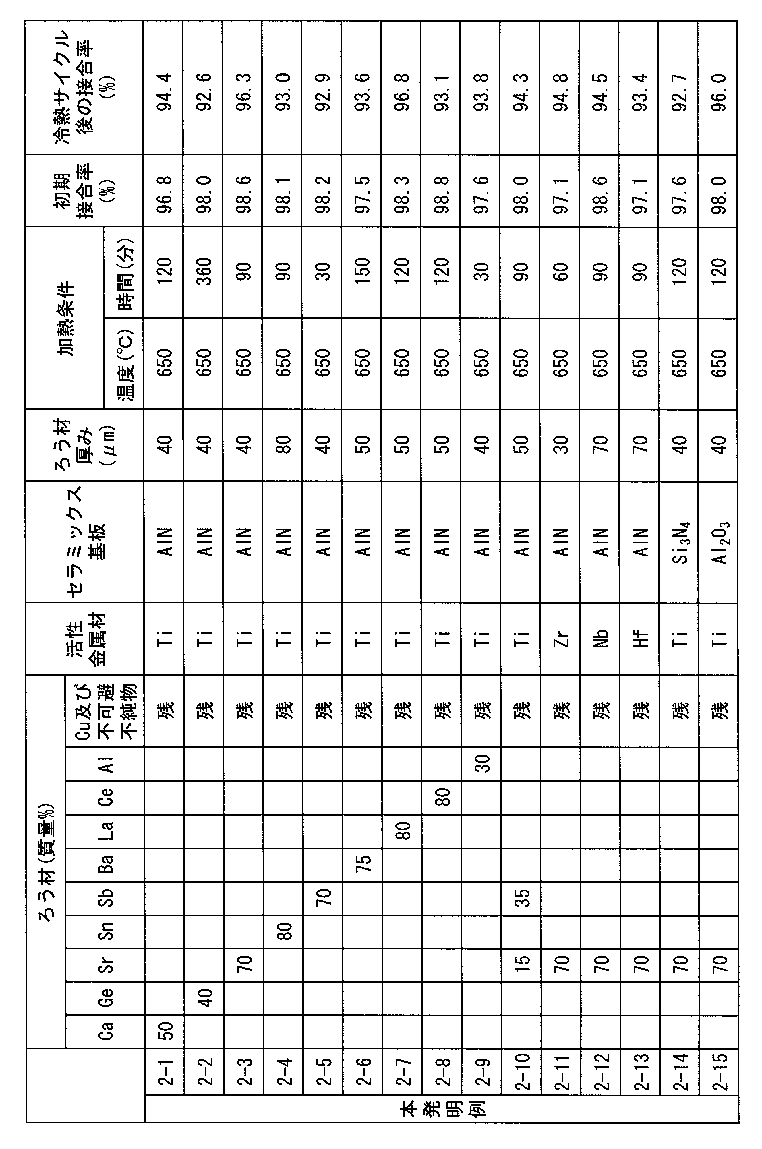
- Example 2 On one surface of the ceramic substrate shown in Table 2 (40 mm ⁇ 40 mm ⁇ thickness 0.635 mm), a Cu plate (37 mm) made of brazing material, active metal material (1 ⁇ m thick foil) shown in Table 2 and oxygen-free copper is provided. ⁇ 37 mm ⁇ thickness 0.3 mm) were laminated in order. Then, an aluminum plate (37 mm ⁇ 37 mm ⁇ thickness 0.6 mm) having a purity of 99.99% or more is laminated on the other surface of the ceramic substrate via an Al-10 mass% Si brazing foil (thickness 20 ⁇ m), A laminate was produced.
- the laminated body is put in a vacuum heating furnace in a state of being pressurized in the laminating direction at a pressure of 15 kgf / cm 2 (1.47 MPa), and heated to place a Cu plate on one surface of the ceramic substrate and on the other surface.
- Aluminum plates were joined.
- the pressure in the vacuum heating furnace was set to 10 ⁇ 3 Pa, and the heating temperature and heating time were set to the conditions shown in Table 2. In this way, power module substrates of Invention Examples 2-1 to 2-15 were obtained.
- the initial bonding rate between the ceramic substrate and the Cu plate and the bonding rate after the thermal cycle test were evaluated.
- a thermal shock tester (TSB-51 manufactured by Espec Co., Ltd.) was used, and it was 5 minutes at ⁇ 40 ° C. for 5 minutes and 125 ° C. for 5 minutes with respect to the power module substrate.
- the cycle of minutes was set to 1 cycle, and 3000 cycles were performed.
- the joining rate was calculated by the same method as in Example 1. The results are shown in Table 2.
- the ceramic member and the Cu member can be satisfactorily joined. Therefore, according to the method for manufacturing a joined body and the method for manufacturing a power module substrate according to the present invention, such as a power semiconductor element for high power control used for controlling an electric vehicle such as wind power generation and an electric vehicle, It is possible to manufacture a bonded body and a power module substrate suitable for a power module having a severe use environment.
Abstract
Description
本願は、2014年4月25日に、日本に出願された特願2014-091955号に基づき優先権を主張し、その内容をここに援用する。
風力発電、電気自動車等の電気車両など、大電力を制御するために用いられるパワー半導体素子は、発熱量が多い。このため、このようなパワー半導体素子を搭載する基板としては、例えば、Si3N4(窒化ケイ素)、AlN(窒化アルミニウム)、Al2O3(アルミナ)など、耐熱性、および絶縁性に優れたセラミックス基板が用いられる。そして、このセラミックス基板の一方の面に、導電性の優れた金属板を回路層として接合したパワーモジュール用基板が、従来から広く用いられている。また、セラミックス基板の他方の面にも、他の金属板を接合することもある。
このセラミックス基板とろう材との接合界面に形成される金属間化合物層は、硬いため、冷熱サイクルが負荷された場合、セラミックス基板と回路層との接合信頼性が低下するおそれがあった。
この構成では、前記加熱工程において溶融したろう材がセラミックス部材と確実に接触することとなり、セラミックス部材とCu部材とを良好に接合することが可能である。
これらの共晶元素を採用することによって、Cuに対して共晶反応させ、ろう材の溶融温度を大きく低下させることが可能になる。従って、低い温度でセラミックス部材とCu部材とを接合することが可能になる。
Cuと、該Cuと共晶反応する元素とからなるろう材を用いれば、Alの融点よりも低い温度でろう材を溶融することができ、セラミックス部材の一方の面にCu部材を接合する工程と、他方の面にAl部材を接合する工程とを一工程で行うことが可能になる。
セラミックス部材としてSi3N4、AlN、Al2O3を選択することで、絶縁性、および放熱性に優れた接合体を製造することができる。
なお、セラミックス基板に接合されたCu板は、回路層、あるいはセラミックス基板における回路層を接合した面とは反対の面に形成された金属層となる。
図1は、本発明の実施形態に係る接合体の製造方法によって得られる接合体の一例を示す断面図である。
接合体10は、図1に示すように、セラミックス部材11と、このセラミックス部材11の一方の面11a(図1において上面)側に配設され、ろう材を介して接合されたCu部材12と、からなる。
ろう材は、Cuと、このCuと共晶反応する共晶元素とからなる。ろう材に用いられる共晶元素は、例えば、Cuとの共晶反応によってAlよりも低い融点を持つ合金を形成する元素から選択される。Cuと共晶反応する元素としては、Ca,Ge,Sr,Sn,Sb,Ba,La,Ce,Al(以下、これら元素は共晶元素と称する)が挙げられる。そして、これら共晶元素のうちから選択される1種または2種以上の元素がろう材に含有される。
Ca:32%以上78%以下(より望ましくは34%以上75%以下)
Ge:37%以上41%以下(より望ましくは38%以上40%以下)
Sr:58%以上93%以下(より望ましくは62%以上90%以下)
Sn:56%以上90%以下(より望ましくは74%以上84%以下)
Sb:52%以上97%以下(より望ましくは57%以上92%以下)
Ba:62%以上95%以下(より望ましくは68%以上91%以下)
La:72%以上89%以下(より望ましくは74%以上87%以下)
Ce:73%以上93%以下(より望ましくは75%以上90%以下)
Al:40%以上95%以下(より望ましくは50%以上85%以下)
すなわち、Alの融点よりも低い接合温度でCu部材12とセラミックス部材11とを接合することができる。
図2は、本発明の実施形態に係る接合体の製造方法を段階的に示した断面図である。
例えば、パワーモジュール用基板として用いられる接合体を製造する際には、まず、Si3N4(窒化ケイ素)、AlN(窒化アルミニウム)、Al2O3(アルミナ)等のセラミックスからなるセラミックス部材21を用意する(図2(a)参照)。本実施形態では、AlNからなり、厚みが0.635mmのセラミックス基板を用いた。
また、Cuと共晶元素との合金粉末を、適切なバインダーを介してペースト状にしたもの(ろう材ペースト)を、セラミックス部材21の一面21aに塗布することもできる。
また、Cuと共晶元素からなる箔状のろう材を、セラミックス部材21と活性金属材23との間に配置することもできる。
なお、活性金属材23の厚さが薄い場合には蒸着を、比較的厚い場合には箔や、ペーストを用いて形成することが好ましい。
本実施形態では、活性金属材として、TiをCu部材24に蒸着することで形成されている。
また、共晶元素のうち、2種以上を選択することによって、ろう材22の融点が上昇することを抑制し、かつろう材22の流動性が低下することを抑え、セラミックス部材21とCu部材24との接合性を更に向上させることができる。
図3、図4は、本発明の実施形態であるパワーモジュール用基板の製造方法を段階的に示した断面図である。
図3(a)に示すように、パワーモジュール用基板を製造する際には、まず、セラミックスからなるセラミックス基板31を用意する。そして、このセラミックス基板31の一面31a側に、ろう材32、活性金属材33、およびCu板34を順に積層する。また、セラミックス部材31の他面31b側に、ろう材35、およびAl板36を順に積層し、積層体37を形成する(積層工程)。
本実施形態では、ろう材32として、上述したろう材22と同じろう材を用いた。
なお、活性金属材33の厚さが薄い場合には蒸着を、比較的厚い場合には箔や、ペーストを用いて形成することが好ましい。
本実施形態では、活性金属材が、TiをCu板34に蒸着することで形成されている。
また、活性金属材33は、ろう材32と一部または全部が混合された状態で、セラミックス基板31とCu板34との間に配置することもできる。
(実施例1)
AlNからなるセラミックス基板(40mm×40mm×厚さ0.635mm)の一方の面に、表1記載のろう材、活性金属材(厚さ6μmの箔)、無酸素銅からなるCu板(37mm×37mm×厚さ0.3mm)を順に積層した。
また、比較例1は、ろう材として、Cuに対して共晶反応を起こさない元素(Ni)を用いた。比較例2は、セラミックス基板とCu板との間にCu箔を介在させる構成とした。
接合率評価は、接合体に対し、セラミックス基板とCu板との界面の接合率について超音波探傷装置(株式会社日立パワーソリューションズ製FineSAT200)を用いて評価し、以下の式から接合率を算出した。
ここで、初期接合面積とは、接合前における接合すべき面積であり、本実施例ではCu板の面積(37mm×37mm)とした。超音波探傷像を二値化処理した画像において剥離は接合部内の白色部で示されることから、この白色部の面積を剥離面積とした。
(接合率(%))={(初期接合面積)-(剥離面積)}/(初期接合面積)×100
以上のような確認実験の結果を表1に示す。

一方、セラミックス基板とCu板との接合の際に、Cuと、このCuと共晶合金を形成しない元素を用いて接合した比較例1や共晶合金を形成する元素を用いなかった比較例2では、セラミックス基板とCu板とが接合されなかった。
表2記載のセラミックス基板(40mm×40mm×厚さ0.635mm)の一方の面に、表2記載のろう材、活性金属材(厚さ1μmの箔)、無酸素銅からなるCu板(37mm×37mm×厚さ0.3mm)を順に積層した。そして、セラミックス基板の他方の面にAl-10質量%Siろう材箔(厚さ20μm)を介して純度99.99%以上のアルミニウム板(37mm×37mm×厚さ0.6mm)を積層し、積層体を作製した。
そして、積層体を積層方向に圧力15kgf/cm2(1.47MPa)で加圧した状態で真空加熱炉に投入し、加熱することによってセラミックス基板の一方の面にCu板を、他方の面にアルミニウム板を接合した。なお、真空加熱炉内の圧力は10-3Paに設定し、加熱温度及び加熱時間は、表2の条件に設定した。このようにして、本発明例2-1~2-15のパワーモジュール用基板を得た。
接合率は実施例1と同様の方法で算出した。
以上の結果を表2に示す。
11 セラミックス部材
12 Cu部材
21 セラミックス部材
22 ろう材
23 活性金属材
24 Cu部材
26 接合体
39 パワーモジュール用基板
Claims (6)
- セラミックスからなるセラミックス部材と、Cu又はCu合金からなるCu部材とが接合されてなる接合体の製造方法であって、
Cuおよび該Cuと共晶反応する共晶元素を含むろう材と、活性金属材とを介して、前記セラミックス部材の一面側に前記Cu部材を積層する積層工程と、
積層された前記セラミックス部材および前記Cu部材を加熱処理する加熱処理工程と、を備えている接合体の製造方法。 - 前記積層工程において、前記セラミックス部材側に前記ろう材を配置し、前記Cu部材側に前記活性金属材を配置する請求項1記載の接合体の製造方法。
- 前記共晶元素は、Ca,Ge,Sr,Sn,Sb,Ba,La,Ce,Alのうちから選択される1種または2種以上の元素である請求項1または2記載の接合体の製造方法。
- 前記積層工程では、前記セラミックス部材の他面側に、Al又はAl合金からなるAl部材を更に積層し、
前記加熱処理工程では、積層された前記セラミックス部材、前記Cu部材、および前記Al部材を加熱処理する請求項1ないし3いずれか一項記載の接合体の製造方法。 - 前記セラミックス部材は、Si3N4、AlN、Al2O3のうち、いずれかより構成される請求項1ないし4いずれか一項記載の接合体の製造方法。
- セラミックス基板の一方の面にCu又はCu合金からなるCu板が配設されたパワーモジュール用基板の製造方法であって、
前記セラミックス基板と前記Cu板とを、請求項1から請求項5いずれか一項に記載の接合体の製造方法によって接合するパワーモジュール用基板の製造方法。
Priority Applications (4)
| Application Number | Priority Date | Filing Date | Title |
|---|---|---|---|
| US15/304,544 US10370303B2 (en) | 2014-04-25 | 2015-04-16 | Process for producing bonded body and process for producing power module substrate |
| EP15783486.2A EP3135653B1 (en) | 2014-04-25 | 2015-04-16 | Process for producing united object and process for producing a substrate for a power module |
| CN201580013381.XA CN106103386A (zh) | 2014-04-25 | 2015-04-16 | 接合体的制造方法及功率模块用基板的制造方法 |
| KR1020167028410A KR102330134B1 (ko) | 2014-04-25 | 2015-04-16 | 접합체의 제조 방법, 파워 모듈용 기판의 제조 방법 |
Applications Claiming Priority (2)
| Application Number | Priority Date | Filing Date | Title |
|---|---|---|---|
| JP2014-091955 | 2014-04-25 | ||
| JP2014091955A JP6256176B2 (ja) | 2014-04-25 | 2014-04-25 | 接合体の製造方法、パワーモジュール用基板の製造方法 |
Publications (1)
| Publication Number | Publication Date |
|---|---|
| WO2015163232A1 true WO2015163232A1 (ja) | 2015-10-29 |
Family
ID=54332398
Family Applications (1)
| Application Number | Title | Priority Date | Filing Date |
|---|---|---|---|
| PCT/JP2015/061719 WO2015163232A1 (ja) | 2014-04-25 | 2015-04-16 | 接合体の製造方法、パワーモジュール用基板の製造方法 |
Country Status (7)
| Country | Link |
|---|---|
| US (1) | US10370303B2 (ja) |
| EP (1) | EP3135653B1 (ja) |
| JP (1) | JP6256176B2 (ja) |
| KR (1) | KR102330134B1 (ja) |
| CN (1) | CN106103386A (ja) |
| TW (1) | TWI642645B (ja) |
| WO (1) | WO2015163232A1 (ja) |
Cited By (1)
| Publication number | Priority date | Publication date | Assignee | Title |
|---|---|---|---|---|
| WO2024071018A1 (ja) * | 2022-09-26 | 2024-04-04 | 日本発條株式会社 | 接合用ろう材および接合体 |
Families Citing this family (5)
| Publication number | Priority date | Publication date | Assignee | Title |
|---|---|---|---|---|
| JP6645368B2 (ja) * | 2016-06-23 | 2020-02-14 | 三菱マテリアル株式会社 | 接合体、パワーモジュール用基板、接合体の製造方法、及び、パワーモジュール用基板の製造方法 |
| WO2020044594A1 (ja) * | 2018-08-28 | 2020-03-05 | 三菱マテリアル株式会社 | 銅/セラミックス接合体、絶縁回路基板、及び、銅/セラミックス接合体の製造方法、及び、絶縁回路基板の製造方法 |
| JP6703584B2 (ja) * | 2018-11-01 | 2020-06-03 | 國家中山科學研究院 | セラミックス搭載板と厚膜回路の接着力を高める方法 |
| DE102019126954A1 (de) * | 2019-10-08 | 2021-04-08 | Rogers Germany Gmbh | Verfahren zur Herstellung eines Metall-Keramik-Substrats, Lötsystem und Metall-Keramik-Substrat, hergestellt mit einem solchen Verfahren |
| DE102019135099A1 (de) * | 2019-12-19 | 2021-06-24 | Rogers Germany Gmbh | Verfahren zur Herstellung eines Metall-Keramik-Substrats und Metall-Keramik-Substrat, hergestellt mit einem solchen Verfahren |
Citations (3)
| Publication number | Priority date | Publication date | Assignee | Title |
|---|---|---|---|---|
| JP2003188310A (ja) * | 2001-12-18 | 2003-07-04 | Denki Kagaku Kogyo Kk | 電極端子付き回路基板の製造方法 |
| JP2003197826A (ja) * | 2001-12-26 | 2003-07-11 | Toshiba Corp | セラミックス回路基板およびそれを用いた半導体モジュール |
| JP2003285195A (ja) * | 2002-03-26 | 2003-10-07 | Ngk Spark Plug Co Ltd | セラミック回路基板及びその製造方法 |
Family Cites Families (16)
| Publication number | Priority date | Publication date | Assignee | Title |
|---|---|---|---|---|
| JPS6081071A (ja) | 1983-10-11 | 1985-05-09 | 三井造船株式会社 | セラミツクス接合用金属シ−ト材 |
| US5403651A (en) * | 1991-10-14 | 1995-04-04 | Fuji Electric Co., Ltd. | Insulating substrate for mounting semiconductor devices |
| JP3495051B2 (ja) * | 1992-07-03 | 2004-02-09 | 株式会社東芝 | セラミックス−金属接合体 |
| JP3866320B2 (ja) | 1995-02-09 | 2007-01-10 | 日本碍子株式会社 | 接合体、および接合体の製造方法 |
| KR100255027B1 (ko) * | 1995-05-17 | 2000-05-01 | 니시무로 타이죠 | 세라믹 금속접합재 및 이를 사용한 세라믹 금속접합체 제조방법 및 이를 이용하여 제작한 진공기밀용기 |
| US6261703B1 (en) * | 1997-05-26 | 2001-07-17 | Sumitomo Electric Industries, Ltd. | Copper circuit junction substrate and method of producing the same |
| JPH11130555A (ja) | 1997-10-28 | 1999-05-18 | Kyocera Corp | セラミックス−銅接合用ろう材 |
| US6660133B2 (en) * | 2002-03-14 | 2003-12-09 | Kennametal Inc. | Nanolayered coated cutting tool and method for making the same |
| JP2004146650A (ja) * | 2002-10-25 | 2004-05-20 | Sumitomo Metal Electronics Devices Inc | パワーモジュール用基板 |
| JP4394477B2 (ja) * | 2003-03-27 | 2010-01-06 | Dowaホールディングス株式会社 | 金属−セラミックス接合基板の製造方法 |
| JP4375730B2 (ja) | 2004-04-23 | 2009-12-02 | 本田技研工業株式会社 | 銅とセラミックス又は炭素基銅複合材料との接合用ろう材及び同接合方法 |
| CN101972901B (zh) * | 2010-10-25 | 2012-06-06 | 北京科技大学 | 一种钎焊铝碳化硅复合材料的中温钎料及制备和钎焊方法 |
| TWI575680B (zh) * | 2011-08-12 | 2017-03-21 | 三菱綜合材料股份有限公司 | 功率模組用基板、附有散熱片功率模組用基板、功率模組及功率模組用基板之製造方法 |
| JP6127540B2 (ja) * | 2012-03-30 | 2017-05-17 | 三菱マテリアル株式会社 | パワーモジュール用基板の製造方法 |
| JP5672324B2 (ja) * | 2013-03-18 | 2015-02-18 | 三菱マテリアル株式会社 | 接合体の製造方法及びパワーモジュール用基板の製造方法 |
| JP6111764B2 (ja) * | 2013-03-18 | 2017-04-12 | 三菱マテリアル株式会社 | パワーモジュール用基板の製造方法 |
-
2014
- 2014-04-25 JP JP2014091955A patent/JP6256176B2/ja active Active
-
2015
- 2015-04-16 US US15/304,544 patent/US10370303B2/en not_active Expired - Fee Related
- 2015-04-16 KR KR1020167028410A patent/KR102330134B1/ko active IP Right Grant
- 2015-04-16 EP EP15783486.2A patent/EP3135653B1/en not_active Not-in-force
- 2015-04-16 WO PCT/JP2015/061719 patent/WO2015163232A1/ja active Application Filing
- 2015-04-16 CN CN201580013381.XA patent/CN106103386A/zh active Pending
- 2015-04-22 TW TW104112861A patent/TWI642645B/zh active
Patent Citations (3)
| Publication number | Priority date | Publication date | Assignee | Title |
|---|---|---|---|---|
| JP2003188310A (ja) * | 2001-12-18 | 2003-07-04 | Denki Kagaku Kogyo Kk | 電極端子付き回路基板の製造方法 |
| JP2003197826A (ja) * | 2001-12-26 | 2003-07-11 | Toshiba Corp | セラミックス回路基板およびそれを用いた半導体モジュール |
| JP2003285195A (ja) * | 2002-03-26 | 2003-10-07 | Ngk Spark Plug Co Ltd | セラミック回路基板及びその製造方法 |
Cited By (1)
| Publication number | Priority date | Publication date | Assignee | Title |
|---|---|---|---|---|
| WO2024071018A1 (ja) * | 2022-09-26 | 2024-04-04 | 日本発條株式会社 | 接合用ろう材および接合体 |
Also Published As
| Publication number | Publication date |
|---|---|
| KR20160148529A (ko) | 2016-12-26 |
| TW201605766A (zh) | 2016-02-16 |
| JP2015209356A (ja) | 2015-11-24 |
| EP3135653B1 (en) | 2018-10-03 |
| EP3135653A1 (en) | 2017-03-01 |
| US20170044072A1 (en) | 2017-02-16 |
| CN106103386A (zh) | 2016-11-09 |
| KR102330134B1 (ko) | 2021-11-22 |
| JP6256176B2 (ja) | 2018-01-10 |
| TWI642645B (zh) | 2018-12-01 |
| US10370303B2 (en) | 2019-08-06 |
| EP3135653A4 (en) | 2017-09-27 |
Similar Documents
| Publication | Publication Date | Title |
|---|---|---|
| KR102459745B1 (ko) | 구리/세라믹스 접합체, 절연 회로 기판, 및, 구리/세라믹스 접합체의 제조 방법, 절연 회로 기판의 제조 방법 | |
| JP6111764B2 (ja) | パワーモジュール用基板の製造方法 | |
| TWI641300B (zh) | 接合體及功率模組用基板 | |
| TWI623065B (zh) | 接合體之製造方法及功率模組用基板之製造方法 | |
| TWI609461B (zh) | 接合體之製造方法及功率模組用基板之製造方法 | |
| WO2015163232A1 (ja) | 接合体の製造方法、パワーモジュール用基板の製造方法 | |
| TWI637466B (zh) | 接合體及功率模組用基板 | |
| TWI619207B (zh) | 接合體、電源模組用基板、電源模組及接合體之製造方法 | |
| TWI569914B (zh) | 接合體及功率模組用基板 | |
| JP2013229545A (ja) | パワーモジュール用基板、ヒートシンク付パワーモジュール用基板、パワーモジュール、及びパワーモジュール用基板の製造方法 | |
| WO2019088222A1 (ja) | 接合体、及び、絶縁回路基板 | |
| JP2017183716A (ja) | ヒートシンク付絶縁回路基板の製造方法、及び、ヒートシンク付絶縁回路基板 | |
| TWI737894B (zh) | 附有散熱片絕緣電路基板之製造方法 | |
| JP5828352B2 (ja) | 銅/セラミックス接合体、及び、パワーモジュール用基板 | |
| JP6343993B2 (ja) | パワーモジュール用基板、およびその製造方法 | |
| JP2019085327A (ja) | 接合体、及び、絶縁回路基板 | |
| JP6645368B2 (ja) | 接合体、パワーモジュール用基板、接合体の製造方法、及び、パワーモジュール用基板の製造方法 | |
| JP5825380B2 (ja) | 銅/セラミックス接合体、及び、パワーモジュール用基板 | |
| JP6561886B2 (ja) | ヒートシンク付パワーモジュール用基板の製造方法 | |
| WO2020045403A1 (ja) | 銅/セラミックス接合体、絶縁回路基板、及び、銅/セラミックス接合体の製造方法、及び、絶縁回路基板の製造方法 | |
| WO2019159257A1 (ja) | セラミックス/Al-SiC複合材料接合体の製造方法、及びヒートシンク付パワーモジュール用基板の製造方法 | |
| JP2018032731A (ja) | ヒートシンク付パワーモジュール用基板、及びヒートシンク付パワーモジュール用基板の製造方法 | |
| TW201934523A (zh) | 陶瓷/鋁-碳化矽複合材料接合體之製造方法、及附散熱塊之功率模組用基板之製造方法 | |
| JP7363027B2 (ja) | 接合体の製造方法、及び、絶縁回路基板の製造方法 | |
| JP6680144B2 (ja) | セラミックス/Al−SiC複合材料接合体の製造方法、及びヒートシンク付パワーモジュール用基板の製造方法 |
Legal Events
| Date | Code | Title | Description |
|---|---|---|---|
| 121 | Ep: the epo has been informed by wipo that ep was designated in this application |
Ref document number: 15783486 Country of ref document: EP Kind code of ref document: A1 |
|
| ENP | Entry into the national phase |
Ref document number: 20167028410 Country of ref document: KR Kind code of ref document: A |
|
| REEP | Request for entry into the european phase |
Ref document number: 2015783486 Country of ref document: EP |
|
| WWE | Wipo information: entry into national phase |
Ref document number: 15304544 Country of ref document: US Ref document number: 2015783486 Country of ref document: EP |
|
| NENP | Non-entry into the national phase |
Ref country code: DE |