WO2015159952A1 - Élément de conversion photoélectrique, cellule solaire l'utilisant et procédé de fabrication d'élément de conversion photoélectrique - Google Patents
Élément de conversion photoélectrique, cellule solaire l'utilisant et procédé de fabrication d'élément de conversion photoélectrique Download PDFInfo
- Publication number
- WO2015159952A1 WO2015159952A1 PCT/JP2015/061724 JP2015061724W WO2015159952A1 WO 2015159952 A1 WO2015159952 A1 WO 2015159952A1 JP 2015061724 W JP2015061724 W JP 2015061724W WO 2015159952 A1 WO2015159952 A1 WO 2015159952A1
- Authority
- WO
- WIPO (PCT)
- Prior art keywords
- group
- formula
- photoelectric conversion
- conversion element
- atom
- Prior art date
Links
- 238000006243 chemical reaction Methods 0.000 title claims abstract description 210
- 238000004519 manufacturing process Methods 0.000 title claims abstract description 40
- 238000000034 method Methods 0.000 title abstract description 40
- 150000001875 compounds Chemical class 0.000 claims abstract description 91
- 125000001424 substituent group Chemical group 0.000 claims abstract description 65
- 239000006096 absorbing agent Substances 0.000 claims abstract description 59
- 125000000217 alkyl group Chemical group 0.000 claims abstract description 53
- 239000013078 crystal Substances 0.000 claims abstract description 44
- 229910052751 metal Inorganic materials 0.000 claims abstract description 44
- 239000002184 metal Substances 0.000 claims abstract description 44
- 150000001450 anions Chemical class 0.000 claims abstract description 40
- 125000004429 atom Chemical group 0.000 claims abstract description 37
- 150000001768 cations Chemical class 0.000 claims abstract description 35
- 125000004435 hydrogen atom Chemical group [H]* 0.000 claims abstract description 32
- 150000002892 organic cations Chemical class 0.000 claims abstract description 31
- 125000005647 linker group Chemical group 0.000 claims abstract description 21
- 239000007788 liquid Substances 0.000 claims abstract description 11
- 230000005525 hole transport Effects 0.000 claims description 58
- 125000003118 aryl group Chemical group 0.000 claims description 29
- 125000001072 heteroaryl group Chemical group 0.000 claims description 23
- 125000005843 halogen group Chemical group 0.000 claims description 17
- 125000003342 alkenyl group Chemical group 0.000 claims description 16
- 125000000304 alkynyl group Chemical group 0.000 claims description 15
- 125000004433 nitrogen atom Chemical group N* 0.000 claims description 15
- 229910052717 sulfur Inorganic materials 0.000 claims description 15
- 125000004434 sulfur atom Chemical group 0.000 claims description 15
- 125000004430 oxygen atom Chemical group O* 0.000 claims description 14
- 125000000753 cycloalkyl group Chemical group 0.000 claims description 13
- 229910052757 nitrogen Inorganic materials 0.000 claims description 12
- 125000000962 organic group Chemical group 0.000 claims description 11
- XEEYBQQBJWHFJM-UHFFFAOYSA-N Iron Chemical compound [Fe] XEEYBQQBJWHFJM-UHFFFAOYSA-N 0.000 claims description 10
- 125000002091 cationic group Chemical group 0.000 claims description 9
- 125000005842 heteroatom Chemical group 0.000 claims description 7
- ATJFFYVFTNAWJD-UHFFFAOYSA-N Tin Chemical compound [Sn] ATJFFYVFTNAWJD-UHFFFAOYSA-N 0.000 claims description 5
- 239000010410 layer Substances 0.000 description 304
- 239000000243 solution Substances 0.000 description 49
- 230000000903 blocking effect Effects 0.000 description 38
- 239000000463 material Substances 0.000 description 37
- 239000010408 film Substances 0.000 description 35
- -1 guanidinium cation Chemical class 0.000 description 34
- LFQSCWFLJHTTHZ-UHFFFAOYSA-N Ethanol Chemical compound CCO LFQSCWFLJHTTHZ-UHFFFAOYSA-N 0.000 description 22
- 125000003277 amino group Chemical group 0.000 description 21
- WEVYAHXRMPXWCK-UHFFFAOYSA-N Acetonitrile Chemical compound CC#N WEVYAHXRMPXWCK-UHFFFAOYSA-N 0.000 description 18
- 125000004432 carbon atom Chemical group C* 0.000 description 18
- OKTJSMMVPCPJKN-UHFFFAOYSA-N Carbon Chemical compound [C] OKTJSMMVPCPJKN-UHFFFAOYSA-N 0.000 description 16
- 239000010419 fine particle Substances 0.000 description 16
- 230000002829 reductive effect Effects 0.000 description 16
- OKKJLVBELUTLKV-UHFFFAOYSA-N Methanol Chemical compound OC OKKJLVBELUTLKV-UHFFFAOYSA-N 0.000 description 15
- ZMXDDKWLCZADIW-UHFFFAOYSA-N N,N-Dimethylformamide Chemical compound CN(C)C=O ZMXDDKWLCZADIW-UHFFFAOYSA-N 0.000 description 15
- 239000002904 solvent Substances 0.000 description 15
- GWEVSGVZZGPLCZ-UHFFFAOYSA-N Titan oxide Chemical compound O=[Ti]=O GWEVSGVZZGPLCZ-UHFFFAOYSA-N 0.000 description 14
- 238000000576 coating method Methods 0.000 description 14
- 239000012043 crude product Substances 0.000 description 13
- QGZKDVFQNNGYKY-UHFFFAOYSA-O Ammonium Chemical compound [NH4+] QGZKDVFQNNGYKY-UHFFFAOYSA-O 0.000 description 12
- RTZKZFJDLAIYFH-UHFFFAOYSA-N Diethyl ether Chemical compound CCOCC RTZKZFJDLAIYFH-UHFFFAOYSA-N 0.000 description 12
- 239000011248 coating agent Substances 0.000 description 11
- 238000010304 firing Methods 0.000 description 11
- 239000000203 mixture Substances 0.000 description 11
- 229920001343 polytetrafluoroethylene Polymers 0.000 description 11
- 239000004810 polytetrafluoroethylene Substances 0.000 description 11
- 239000006185 dispersion Substances 0.000 description 9
- 239000011521 glass Substances 0.000 description 9
- 239000002245 particle Substances 0.000 description 8
- 239000010409 thin film Substances 0.000 description 8
- 239000011135 tin Substances 0.000 description 8
- OGIDPMRJRNCKJF-UHFFFAOYSA-N titanium oxide Inorganic materials [Ti]=O OGIDPMRJRNCKJF-UHFFFAOYSA-N 0.000 description 8
- 239000002250 absorbent Substances 0.000 description 7
- 230000002745 absorbent Effects 0.000 description 7
- 125000002252 acyl group Chemical group 0.000 description 7
- 239000002041 carbon nanotube Substances 0.000 description 7
- 229910021393 carbon nanotube Inorganic materials 0.000 description 7
- 238000001914 filtration Methods 0.000 description 7
- BASFCYQUMIYNBI-UHFFFAOYSA-N platinum Chemical compound [Pt] BASFCYQUMIYNBI-UHFFFAOYSA-N 0.000 description 7
- 229910052718 tin Inorganic materials 0.000 description 7
- BAVYZALUXZFZLV-UHFFFAOYSA-N Methylamine Chemical compound NC BAVYZALUXZFZLV-UHFFFAOYSA-N 0.000 description 6
- PXHVJJICTQNCMI-UHFFFAOYSA-N Nickel Chemical compound [Ni] PXHVJJICTQNCMI-UHFFFAOYSA-N 0.000 description 6
- KDLHZDBZIXYQEI-UHFFFAOYSA-N Palladium Chemical compound [Pd] KDLHZDBZIXYQEI-UHFFFAOYSA-N 0.000 description 6
- 238000001035 drying Methods 0.000 description 6
- 125000000623 heterocyclic group Chemical group 0.000 description 6
- 150000002500 ions Chemical class 0.000 description 6
- 229910044991 metal oxide Inorganic materials 0.000 description 6
- 150000004706 metal oxides Chemical class 0.000 description 6
- 239000004033 plastic Substances 0.000 description 6
- 229920003023 plastic Polymers 0.000 description 6
- 239000011148 porous material Substances 0.000 description 6
- 239000004065 semiconductor Substances 0.000 description 6
- XOLBLPGZBRYERU-UHFFFAOYSA-N tin dioxide Chemical compound O=[Sn]=O XOLBLPGZBRYERU-UHFFFAOYSA-N 0.000 description 6
- 229910001887 tin oxide Inorganic materials 0.000 description 6
- VYPSYNLAJGMNEJ-UHFFFAOYSA-N Silicium dioxide Chemical compound O=[Si]=O VYPSYNLAJGMNEJ-UHFFFAOYSA-N 0.000 description 5
- MVPPADPHJFYWMZ-UHFFFAOYSA-N chlorobenzene Chemical compound ClC1=CC=CC=C1 MVPPADPHJFYWMZ-UHFFFAOYSA-N 0.000 description 5
- 229910052731 fluorine Inorganic materials 0.000 description 5
- 125000001153 fluoro group Chemical group F* 0.000 description 5
- 229910021389 graphene Inorganic materials 0.000 description 5
- 238000010438 heat treatment Methods 0.000 description 5
- XMBWDFGMSWQBCA-UHFFFAOYSA-N hydrogen iodide Chemical compound I XMBWDFGMSWQBCA-UHFFFAOYSA-N 0.000 description 5
- 229940071870 hydroiodic acid Drugs 0.000 description 5
- 125000001841 imino group Chemical group [H]N=* 0.000 description 5
- 239000012212 insulator Substances 0.000 description 5
- 230000009467 reduction Effects 0.000 description 5
- 239000000126 substance Substances 0.000 description 5
- 125000000547 substituted alkyl group Chemical group 0.000 description 5
- ZCYVEMRRCGMTRW-UHFFFAOYSA-N 7553-56-2 Chemical group [I] ZCYVEMRRCGMTRW-UHFFFAOYSA-N 0.000 description 4
- WKBOTKDWSSQWDR-UHFFFAOYSA-N Bromine atom Chemical group [Br] WKBOTKDWSSQWDR-UHFFFAOYSA-N 0.000 description 4
- KFZMGEQAYNKOFK-UHFFFAOYSA-N Isopropanol Chemical compound CC(C)O KFZMGEQAYNKOFK-UHFFFAOYSA-N 0.000 description 4
- 150000004770 chalcogenides Chemical class 0.000 description 4
- 229910052801 chlorine Inorganic materials 0.000 description 4
- 125000001309 chloro group Chemical group Cl* 0.000 description 4
- 239000004020 conductor Substances 0.000 description 4
- 239000010949 copper Substances 0.000 description 4
- 125000004093 cyano group Chemical group *C#N 0.000 description 4
- 230000000694 effects Effects 0.000 description 4
- 238000011156 evaluation Methods 0.000 description 4
- 239000010931 gold Substances 0.000 description 4
- 229910052740 iodine Inorganic materials 0.000 description 4
- 125000002496 methyl group Chemical group [H]C([H])([H])* 0.000 description 4
- 239000012046 mixed solvent Substances 0.000 description 4
- 239000011368 organic material Substances 0.000 description 4
- TWNQGVIAIRXVLR-UHFFFAOYSA-N oxo(oxoalumanyloxy)alumane Chemical compound O=[Al]O[Al]=O TWNQGVIAIRXVLR-UHFFFAOYSA-N 0.000 description 4
- 238000004528 spin coating Methods 0.000 description 4
- 239000000758 substrate Substances 0.000 description 4
- JYEUMXHLPRZUAT-UHFFFAOYSA-N 1,2,3-triazine Chemical group C1=CN=NN=C1 JYEUMXHLPRZUAT-UHFFFAOYSA-N 0.000 description 3
- BAVYZALUXZFZLV-UHFFFAOYSA-O Methylammonium ion Chemical compound [NH3+]C BAVYZALUXZFZLV-UHFFFAOYSA-O 0.000 description 3
- JUJWROOIHBZHMG-UHFFFAOYSA-N Pyridine Chemical group C1=CC=NC=C1 JUJWROOIHBZHMG-UHFFFAOYSA-N 0.000 description 3
- YTPLMLYBLZKORZ-UHFFFAOYSA-N Thiophene Chemical group C=1C=CSC=1 YTPLMLYBLZKORZ-UHFFFAOYSA-N 0.000 description 3
- RTAQQCXQSZGOHL-UHFFFAOYSA-N Titanium Chemical group [Ti] RTAQQCXQSZGOHL-UHFFFAOYSA-N 0.000 description 3
- 229910052782 aluminium Inorganic materials 0.000 description 3
- XAGFODPZIPBFFR-UHFFFAOYSA-N aluminium Chemical compound [Al] XAGFODPZIPBFFR-UHFFFAOYSA-N 0.000 description 3
- AOWKSNWVBZGMTJ-UHFFFAOYSA-N calcium titanate Chemical compound [Ca+2].[O-][Ti]([O-])=O AOWKSNWVBZGMTJ-UHFFFAOYSA-N 0.000 description 3
- 229910052799 carbon Inorganic materials 0.000 description 3
- 230000006866 deterioration Effects 0.000 description 3
- 239000000975 dye Substances 0.000 description 3
- PCHJSUWPFVWCPO-UHFFFAOYSA-N gold Chemical compound [Au] PCHJSUWPFVWCPO-UHFFFAOYSA-N 0.000 description 3
- 229910052737 gold Inorganic materials 0.000 description 3
- 229910052738 indium Inorganic materials 0.000 description 3
- APFVFJFRJDLVQX-UHFFFAOYSA-N indium atom Chemical compound [In] APFVFJFRJDLVQX-UHFFFAOYSA-N 0.000 description 3
- 229910052745 lead Inorganic materials 0.000 description 3
- VNWKTOKETHGBQD-UHFFFAOYSA-N methane Chemical compound C VNWKTOKETHGBQD-UHFFFAOYSA-N 0.000 description 3
- 229910052697 platinum Inorganic materials 0.000 description 3
- 230000002265 prevention Effects 0.000 description 3
- 230000008569 process Effects 0.000 description 3
- 238000007650 screen-printing Methods 0.000 description 3
- 229910052814 silicon oxide Inorganic materials 0.000 description 3
- 239000007787 solid Substances 0.000 description 3
- 238000003756 stirring Methods 0.000 description 3
- 238000012360 testing method Methods 0.000 description 3
- 125000003441 thioacyl group Chemical group 0.000 description 3
- XDXWNHPWWKGTKO-UHFFFAOYSA-N 207739-72-8 Chemical compound C1=CC(OC)=CC=C1N(C=1C=C2C3(C4=CC(=CC=C4C2=CC=1)N(C=1C=CC(OC)=CC=1)C=1C=CC(OC)=CC=1)C1=CC(=CC=C1C1=CC=C(C=C13)N(C=1C=CC(OC)=CC=1)C=1C=CC(OC)=CC=1)N(C=1C=CC(OC)=CC=1)C=1C=CC(OC)=CC=1)C1=CC=C(OC)C=C1 XDXWNHPWWKGTKO-UHFFFAOYSA-N 0.000 description 2
- BMYNFMYTOJXKLE-UHFFFAOYSA-N 3-azaniumyl-2-hydroxypropanoate Chemical compound NCC(O)C(O)=O BMYNFMYTOJXKLE-UHFFFAOYSA-N 0.000 description 2
- YEJRWHAVMIAJKC-UHFFFAOYSA-N 4-Butyrolactone Chemical compound O=C1CCCO1 YEJRWHAVMIAJKC-UHFFFAOYSA-N 0.000 description 2
- XMWRBQBLMFGWIX-UHFFFAOYSA-N C60 fullerene Chemical class C12=C3C(C4=C56)=C7C8=C5C5=C9C%10=C6C6=C4C1=C1C4=C6C6=C%10C%10=C9C9=C%11C5=C8C5=C8C7=C3C3=C7C2=C1C1=C2C4=C6C4=C%10C6=C9C9=C%11C5=C5C8=C3C3=C7C1=C1C2=C4C6=C2C9=C5C3=C12 XMWRBQBLMFGWIX-UHFFFAOYSA-N 0.000 description 2
- VTYYLEPIZMXCLO-UHFFFAOYSA-L Calcium carbonate Chemical compound [Ca+2].[O-]C([O-])=O VTYYLEPIZMXCLO-UHFFFAOYSA-L 0.000 description 2
- 239000004215 Carbon black (E152) Substances 0.000 description 2
- RYGMFSIKBFXOCR-UHFFFAOYSA-N Copper Chemical compound [Cu] RYGMFSIKBFXOCR-UHFFFAOYSA-N 0.000 description 2
- QUSNBJAOOMFDIB-UHFFFAOYSA-N Ethylamine Chemical compound CCN QUSNBJAOOMFDIB-UHFFFAOYSA-N 0.000 description 2
- YLQBMQCUIZJEEH-UHFFFAOYSA-N Furan Chemical group C=1C=COC=1 YLQBMQCUIZJEEH-UHFFFAOYSA-N 0.000 description 2
- 229920001609 Poly(3,4-ethylenedioxythiophene) Polymers 0.000 description 2
- 229910006404 SnO 2 Inorganic materials 0.000 description 2
- FZWLAAWBMGSTSO-UHFFFAOYSA-N Thiazole Chemical group C1=CSC=N1 FZWLAAWBMGSTSO-UHFFFAOYSA-N 0.000 description 2
- 229910010413 TiO 2 Inorganic materials 0.000 description 2
- HCHKCACWOHOZIP-UHFFFAOYSA-N Zinc Chemical compound [Zn] HCHKCACWOHOZIP-UHFFFAOYSA-N 0.000 description 2
- XLOMVQKBTHCTTD-UHFFFAOYSA-N Zinc monoxide Chemical compound [Zn]=O XLOMVQKBTHCTTD-UHFFFAOYSA-N 0.000 description 2
- QCWXUUIWCKQGHC-UHFFFAOYSA-N Zirconium Chemical compound [Zr] QCWXUUIWCKQGHC-UHFFFAOYSA-N 0.000 description 2
- 125000002723 alicyclic group Chemical group 0.000 description 2
- 125000003545 alkoxy group Chemical group 0.000 description 2
- 125000004453 alkoxycarbonyl group Chemical group 0.000 description 2
- 125000005196 alkyl carbonyloxy group Chemical group 0.000 description 2
- 125000004414 alkyl thio group Chemical group 0.000 description 2
- 150000001408 amides Chemical class 0.000 description 2
- 150000001410 amidinium cations Chemical class 0.000 description 2
- 239000012491 analyte Substances 0.000 description 2
- 125000005199 aryl carbonyloxy group Chemical group 0.000 description 2
- 125000005161 aryl oxy carbonyl group Chemical group 0.000 description 2
- 125000004104 aryloxy group Chemical group 0.000 description 2
- 229910002113 barium titanate Inorganic materials 0.000 description 2
- 239000011575 calcium Substances 0.000 description 2
- 125000003739 carbamimidoyl group Chemical group C(N)(=N)* 0.000 description 2
- 125000003917 carbamoyl group Chemical group [H]N([H])C(*)=O 0.000 description 2
- 150000001721 carbon Chemical group 0.000 description 2
- 239000003575 carbonaceous material Substances 0.000 description 2
- 229920001940 conductive polymer Polymers 0.000 description 2
- 239000000470 constituent Substances 0.000 description 2
- 229910052802 copper Inorganic materials 0.000 description 2
- 230000007547 defect Effects 0.000 description 2
- 238000007598 dipping method Methods 0.000 description 2
- 239000002612 dispersion medium Substances 0.000 description 2
- POULHZVOKOAJMA-UHFFFAOYSA-N dodecanoic acid Chemical compound CCCCCCCCCCCC(O)=O POULHZVOKOAJMA-UHFFFAOYSA-N 0.000 description 2
- 239000002079 double walled nanotube Substances 0.000 description 2
- 125000001495 ethyl group Chemical group [H]C([H])([H])C([H])([H])* 0.000 description 2
- 125000004005 formimidoyl group Chemical group [H]\N=C(/[H])* 0.000 description 2
- 229930195733 hydrocarbon Natural products 0.000 description 2
- 150000002430 hydrocarbons Chemical class 0.000 description 2
- 125000002883 imidazolyl group Chemical group 0.000 description 2
- 239000011810 insulating material Substances 0.000 description 2
- 230000031700 light absorption Effects 0.000 description 2
- 239000000395 magnesium oxide Substances 0.000 description 2
- CPLXHLVBOLITMK-UHFFFAOYSA-N magnesium oxide Inorganic materials [Mg]=O CPLXHLVBOLITMK-UHFFFAOYSA-N 0.000 description 2
- AXZKOIWUVFPNLO-UHFFFAOYSA-N magnesium;oxygen(2-) Chemical compound [O-2].[Mg+2] AXZKOIWUVFPNLO-UHFFFAOYSA-N 0.000 description 2
- 239000011572 manganese Substances 0.000 description 2
- 229910001507 metal halide Inorganic materials 0.000 description 2
- 150000005309 metal halides Chemical class 0.000 description 2
- 238000002156 mixing Methods 0.000 description 2
- 239000002048 multi walled nanotube Substances 0.000 description 2
- 229910052759 nickel Inorganic materials 0.000 description 2
- 150000002825 nitriles Chemical class 0.000 description 2
- 125000002971 oxazolyl group Chemical group 0.000 description 2
- 239000007800 oxidant agent Substances 0.000 description 2
- 230000001590 oxidative effect Effects 0.000 description 2
- 229910052763 palladium Inorganic materials 0.000 description 2
- 125000002080 perylenyl group Chemical group C1(=CC=C2C=CC=C3C4=CC=CC5=CC=CC(C1=C23)=C45)* 0.000 description 2
- 125000001997 phenyl group Chemical group [H]C1=C([H])C([H])=C(*)C([H])=C1[H] 0.000 description 2
- 239000002243 precursor Substances 0.000 description 2
- 238000007639 printing Methods 0.000 description 2
- 125000003373 pyrazinyl group Chemical group 0.000 description 2
- 125000003226 pyrazolyl group Chemical group 0.000 description 2
- 125000000714 pyrimidinyl group Chemical group 0.000 description 2
- 125000000168 pyrrolyl group Chemical group 0.000 description 2
- 230000002441 reversible effect Effects 0.000 description 2
- 239000010948 rhodium Substances 0.000 description 2
- 229910052710 silicon Inorganic materials 0.000 description 2
- 239000002356 single layer Substances 0.000 description 2
- 239000002109 single walled nanotube Substances 0.000 description 2
- 238000005118 spray pyrolysis Methods 0.000 description 2
- 229910052712 strontium Inorganic materials 0.000 description 2
- CIOAGBVUUVVLOB-UHFFFAOYSA-N strontium atom Chemical compound [Sr] CIOAGBVUUVVLOB-UHFFFAOYSA-N 0.000 description 2
- VEALVRVVWBQVSL-UHFFFAOYSA-N strontium titanate Chemical compound [Sr+2].[O-][Ti]([O-])=O VEALVRVVWBQVSL-UHFFFAOYSA-N 0.000 description 2
- 238000006467 substitution reaction Methods 0.000 description 2
- 125000000446 sulfanediyl group Chemical group *S* 0.000 description 2
- 229910052719 titanium Inorganic materials 0.000 description 2
- 239000010936 titanium Substances 0.000 description 2
- 125000001425 triazolyl group Chemical group 0.000 description 2
- 238000007740 vapor deposition Methods 0.000 description 2
- 229910052725 zinc Inorganic materials 0.000 description 2
- 239000011701 zinc Substances 0.000 description 2
- 229910052726 zirconium Inorganic materials 0.000 description 2
- DYLIWHYUXAJDOJ-OWOJBTEDSA-N (e)-4-(6-aminopurin-9-yl)but-2-en-1-ol Chemical compound NC1=NC=NC2=C1N=CN2C\C=C\CO DYLIWHYUXAJDOJ-OWOJBTEDSA-N 0.000 description 1
- OLRBYEHWZZSYQQ-VVDZMTNVSA-N (e)-4-hydroxypent-3-en-2-one;propan-2-ol;titanium Chemical compound [Ti].CC(C)O.CC(C)O.C\C(O)=C/C(C)=O.C\C(O)=C/C(C)=O OLRBYEHWZZSYQQ-VVDZMTNVSA-N 0.000 description 1
- UGUHFDPGDQDVGX-UHFFFAOYSA-N 1,2,3-thiadiazole Chemical group C1=CSN=N1 UGUHFDPGDQDVGX-UHFFFAOYSA-N 0.000 description 1
- 125000000355 1,3-benzoxazolyl group Chemical group O1C(=NC2=C1C=CC=C2)* 0.000 description 1
- 125000006021 1-methyl-2-propenyl group Chemical group 0.000 description 1
- FFQALBCXGPYQGT-UHFFFAOYSA-N 2,4-difluoro-5-(trifluoromethyl)aniline Chemical compound NC1=CC(C(F)(F)F)=C(F)C=C1F FFQALBCXGPYQGT-UHFFFAOYSA-N 0.000 description 1
- 125000003903 2-propenyl group Chemical group [H]C([*])([H])C([H])=C([H])[H] 0.000 description 1
- UUIMDJFBHNDZOW-UHFFFAOYSA-N 2-tert-butylpyridine Chemical compound CC(C)(C)C1=CC=CC=N1 UUIMDJFBHNDZOW-UHFFFAOYSA-N 0.000 description 1
- WUPHOULIZUERAE-UHFFFAOYSA-N 3-(oxolan-2-yl)propanoic acid Chemical compound OC(=O)CCC1CCCO1 WUPHOULIZUERAE-UHFFFAOYSA-N 0.000 description 1
- MNFZZNNFORDXSV-UHFFFAOYSA-N 4-(diethylamino)benzaldehyde Chemical compound CCN(CC)C1=CC=C(C=O)C=C1 MNFZZNNFORDXSV-UHFFFAOYSA-N 0.000 description 1
- 229910018072 Al 2 O 3 Inorganic materials 0.000 description 1
- ROFVEXUMMXZLPA-UHFFFAOYSA-N Bipyridyl Chemical group N1=CC=CC=C1C1=CC=CC=N1 ROFVEXUMMXZLPA-UHFFFAOYSA-N 0.000 description 1
- NLZUEZXRPGMBCV-UHFFFAOYSA-N Butylhydroxytoluene Chemical compound CC1=CC(C(C)(C)C)=C(O)C(C(C)(C)C)=C1 NLZUEZXRPGMBCV-UHFFFAOYSA-N 0.000 description 1
- OYPRJOBELJOOCE-UHFFFAOYSA-N Calcium Chemical compound [Ca] OYPRJOBELJOOCE-UHFFFAOYSA-N 0.000 description 1
- 229910052684 Cerium Inorganic materials 0.000 description 1
- 229910020366 ClO 4 Inorganic materials 0.000 description 1
- 239000001856 Ethyl cellulose Substances 0.000 description 1
- ZZSNKZQZMQGXPY-UHFFFAOYSA-N Ethyl cellulose Chemical compound CCOCC1OC(OC)C(OCC)C(OCC)C1OC1C(O)C(O)C(OC)C(CO)O1 ZZSNKZQZMQGXPY-UHFFFAOYSA-N 0.000 description 1
- PIICEJLVQHRZGT-UHFFFAOYSA-N Ethylenediamine Chemical compound NCCN PIICEJLVQHRZGT-UHFFFAOYSA-N 0.000 description 1
- 229910052693 Europium Inorganic materials 0.000 description 1
- PNKUSGQVOMIXLU-UHFFFAOYSA-N Formamidine Chemical compound NC=N PNKUSGQVOMIXLU-UHFFFAOYSA-N 0.000 description 1
- 239000005639 Lauric acid Substances 0.000 description 1
- PWHULOQIROXLJO-UHFFFAOYSA-N Manganese Chemical compound [Mn] PWHULOQIROXLJO-UHFFFAOYSA-N 0.000 description 1
- FXHOOIRPVKKKFG-UHFFFAOYSA-N N,N-Dimethylacetamide Chemical compound CN(C)C(C)=O FXHOOIRPVKKKFG-UHFFFAOYSA-N 0.000 description 1
- 239000004372 Polyvinyl alcohol Substances 0.000 description 1
- KJTLSVCANCCWHF-UHFFFAOYSA-N Ruthenium Chemical compound [Ru] KJTLSVCANCCWHF-UHFFFAOYSA-N 0.000 description 1
- BQCADISMDOOEFD-UHFFFAOYSA-N Silver Chemical compound [Ag] BQCADISMDOOEFD-UHFFFAOYSA-N 0.000 description 1
- 229910052769 Ytterbium Inorganic materials 0.000 description 1
- 229910021536 Zeolite Inorganic materials 0.000 description 1
- WOIHABYNKOEWFG-UHFFFAOYSA-N [Sr].[Ba] Chemical compound [Sr].[Ba] WOIHABYNKOEWFG-UHFFFAOYSA-N 0.000 description 1
- XPOLVIIHTDKJRY-UHFFFAOYSA-N acetic acid;methanimidamide Chemical compound NC=N.CC(O)=O XPOLVIIHTDKJRY-UHFFFAOYSA-N 0.000 description 1
- 125000000783 acetimidoyl group Chemical group C(C)(=N)* 0.000 description 1
- 125000002777 acetyl group Chemical group [H]C([H])([H])C(*)=O 0.000 description 1
- 239000002253 acid Substances 0.000 description 1
- 125000004442 acylamino group Chemical group 0.000 description 1
- 239000000654 additive Substances 0.000 description 1
- 239000000853 adhesive Substances 0.000 description 1
- 230000001070 adhesive effect Effects 0.000 description 1
- 125000001931 aliphatic group Chemical group 0.000 description 1
- HSFWRNGVRCDJHI-UHFFFAOYSA-N alpha-acetylene Natural products C#C HSFWRNGVRCDJHI-UHFFFAOYSA-N 0.000 description 1
- WUOACPNHFRMFPN-UHFFFAOYSA-N alpha-terpineol Chemical compound CC1=CCC(C(C)(C)O)CC1 WUOACPNHFRMFPN-UHFFFAOYSA-N 0.000 description 1
- 150000001412 amines Chemical class 0.000 description 1
- 125000004397 aminosulfonyl group Chemical group NS(=O)(=O)* 0.000 description 1
- 125000000129 anionic group Chemical group 0.000 description 1
- 238000000137 annealing Methods 0.000 description 1
- 239000007864 aqueous solution Substances 0.000 description 1
- 239000012298 atmosphere Substances 0.000 description 1
- QVGXLLKOCUKJST-UHFFFAOYSA-N atomic oxygen Chemical compound [O] QVGXLLKOCUKJST-UHFFFAOYSA-N 0.000 description 1
- 229910052788 barium Inorganic materials 0.000 description 1
- IQONKZQQCCPWMS-UHFFFAOYSA-N barium lanthanum Chemical compound [Ba].[La] IQONKZQQCCPWMS-UHFFFAOYSA-N 0.000 description 1
- JRPBQTZRNDNNOP-UHFFFAOYSA-N barium titanate Chemical compound [Ba+2].[Ba+2].[O-][Ti]([O-])([O-])[O-] JRPBQTZRNDNNOP-UHFFFAOYSA-N 0.000 description 1
- 229910021523 barium zirconate Inorganic materials 0.000 description 1
- DQBAOWPVHRWLJC-UHFFFAOYSA-N barium(2+);dioxido(oxo)zirconium Chemical compound [Ba+2].[O-][Zr]([O-])=O DQBAOWPVHRWLJC-UHFFFAOYSA-N 0.000 description 1
- 125000003785 benzimidazolyl group Chemical group N1=C(NC2=C1C=CC=C2)* 0.000 description 1
- IOJUPLGTWVMSFF-UHFFFAOYSA-N benzothiazole Chemical group C1=CC=C2SC=NC2=C1 IOJUPLGTWVMSFF-UHFFFAOYSA-N 0.000 description 1
- 229910052797 bismuth Inorganic materials 0.000 description 1
- JCXGWMGPZLAOME-UHFFFAOYSA-N bismuth atom Chemical compound [Bi] JCXGWMGPZLAOME-UHFFFAOYSA-N 0.000 description 1
- 229910002115 bismuth titanate Inorganic materials 0.000 description 1
- 125000004369 butenyl group Chemical group C(=CCC)* 0.000 description 1
- 125000000480 butynyl group Chemical group [*]C#CC([H])([H])C([H])([H])[H] 0.000 description 1
- 229910052793 cadmium Inorganic materials 0.000 description 1
- BDOSMKKIYDKNTQ-UHFFFAOYSA-N cadmium atom Chemical compound [Cd] BDOSMKKIYDKNTQ-UHFFFAOYSA-N 0.000 description 1
- 229910052980 cadmium sulfide Inorganic materials 0.000 description 1
- UHYPYGJEEGLRJD-UHFFFAOYSA-N cadmium(2+);selenium(2-) Chemical compound [Se-2].[Cd+2] UHYPYGJEEGLRJD-UHFFFAOYSA-N 0.000 description 1
- FJDQFPXHSGXQBY-UHFFFAOYSA-L caesium carbonate Chemical compound [Cs+].[Cs+].[O-]C([O-])=O FJDQFPXHSGXQBY-UHFFFAOYSA-L 0.000 description 1
- 229910000024 caesium carbonate Inorganic materials 0.000 description 1
- 229910052791 calcium Inorganic materials 0.000 description 1
- 229910000019 calcium carbonate Inorganic materials 0.000 description 1
- 125000003178 carboxy group Chemical group [H]OC(*)=O 0.000 description 1
- 239000000919 ceramic Substances 0.000 description 1
- ZMIGMASIKSOYAM-UHFFFAOYSA-N cerium Chemical compound [Ce][Ce][Ce][Ce][Ce][Ce][Ce][Ce][Ce][Ce][Ce][Ce][Ce][Ce][Ce][Ce][Ce][Ce][Ce][Ce][Ce][Ce][Ce][Ce][Ce][Ce][Ce][Ce][Ce][Ce][Ce][Ce][Ce][Ce][Ce][Ce][Ce][Ce] ZMIGMASIKSOYAM-UHFFFAOYSA-N 0.000 description 1
- 239000003795 chemical substances by application Substances 0.000 description 1
- 239000000460 chlorine Substances 0.000 description 1
- 150000008422 chlorobenzenes Chemical class 0.000 description 1
- 229910017052 cobalt Inorganic materials 0.000 description 1
- 239000010941 cobalt Substances 0.000 description 1
- GUTLYIVDDKVIGB-UHFFFAOYSA-N cobalt atom Chemical compound [Co] GUTLYIVDDKVIGB-UHFFFAOYSA-N 0.000 description 1
- 238000007796 conventional method Methods 0.000 description 1
- 238000007766 curtain coating Methods 0.000 description 1
- 125000004966 cyanoalkyl group Chemical group 0.000 description 1
- 125000000113 cyclohexyl group Chemical group [H]C1([H])C([H])([H])C([H])([H])C([H])(*)C([H])([H])C1([H])[H] 0.000 description 1
- 125000001511 cyclopentyl group Chemical group [H]C1([H])C([H])([H])C([H])([H])C([H])(*)C1([H])[H] 0.000 description 1
- 125000001559 cyclopropyl group Chemical group [H]C1([H])C([H])([H])C1([H])* 0.000 description 1
- 230000002950 deficient Effects 0.000 description 1
- SQIFACVGCPWBQZ-UHFFFAOYSA-N delta-terpineol Natural products CC(C)(O)C1CCC(=C)CC1 SQIFACVGCPWBQZ-UHFFFAOYSA-N 0.000 description 1
- 230000000779 depleting effect Effects 0.000 description 1
- 238000007607 die coating method Methods 0.000 description 1
- NKZSPGSOXYXWQA-UHFFFAOYSA-N dioxido(oxo)titanium;lead(2+) Chemical compound [Pb+2].[O-][Ti]([O-])=O NKZSPGSOXYXWQA-UHFFFAOYSA-N 0.000 description 1
- HNPSIPDUKPIQMN-UHFFFAOYSA-N dioxosilane;oxo(oxoalumanyloxy)alumane Chemical compound O=[Si]=O.O=[Al]O[Al]=O HNPSIPDUKPIQMN-UHFFFAOYSA-N 0.000 description 1
- 238000003618 dip coating Methods 0.000 description 1
- 239000002270 dispersing agent Substances 0.000 description 1
- IVUXZQJWTQMSQN-UHFFFAOYSA-N distrontium;oxygen(2-);tantalum(5+) Chemical compound [O-2].[O-2].[O-2].[O-2].[O-2].[O-2].[O-2].[Sr+2].[Sr+2].[Ta+5].[Ta+5] IVUXZQJWTQMSQN-UHFFFAOYSA-N 0.000 description 1
- 239000003792 electrolyte Substances 0.000 description 1
- 239000008151 electrolyte solution Substances 0.000 description 1
- 229920001249 ethyl cellulose Polymers 0.000 description 1
- 235000019325 ethyl cellulose Nutrition 0.000 description 1
- 125000002534 ethynyl group Chemical group [H]C#C* 0.000 description 1
- OGPBJKLSAFTDLK-UHFFFAOYSA-N europium atom Chemical compound [Eu] OGPBJKLSAFTDLK-UHFFFAOYSA-N 0.000 description 1
- 230000005284 excitation Effects 0.000 description 1
- 238000001125 extrusion Methods 0.000 description 1
- XUCNUKMRBVNAPB-UHFFFAOYSA-N fluoroethene Chemical group FC=C XUCNUKMRBVNAPB-UHFFFAOYSA-N 0.000 description 1
- 125000002485 formyl group Chemical group [H]C(*)=O 0.000 description 1
- 229910003472 fullerene Inorganic materials 0.000 description 1
- 229910052732 germanium Inorganic materials 0.000 description 1
- GNPVGFCGXDBREM-UHFFFAOYSA-N germanium atom Chemical compound [Ge] GNPVGFCGXDBREM-UHFFFAOYSA-N 0.000 description 1
- 229910002804 graphite Inorganic materials 0.000 description 1
- 239000010439 graphite Substances 0.000 description 1
- 230000005283 ground state Effects 0.000 description 1
- 229910052735 hafnium Inorganic materials 0.000 description 1
- VBJZVLUMGGDVMO-UHFFFAOYSA-N hafnium atom Chemical compound [Hf] VBJZVLUMGGDVMO-UHFFFAOYSA-N 0.000 description 1
- 229910052736 halogen Inorganic materials 0.000 description 1
- 150000002367 halogens Chemical class 0.000 description 1
- 125000003104 hexanoyl group Chemical group O=C([*])C([H])([H])C([H])([H])C([H])([H])C([H])([H])C([H])([H])[H] 0.000 description 1
- 125000006038 hexenyl group Chemical group 0.000 description 1
- 125000005980 hexynyl group Chemical group 0.000 description 1
- 125000002887 hydroxy group Chemical group [H]O* 0.000 description 1
- 238000007654 immersion Methods 0.000 description 1
- 230000006872 improvement Effects 0.000 description 1
- 125000003453 indazolyl group Chemical group N1N=C(C2=C1C=CC=C2)* 0.000 description 1
- 229910003437 indium oxide Inorganic materials 0.000 description 1
- PJXISJQVUVHSOJ-UHFFFAOYSA-N indium(iii) oxide Chemical compound [O-2].[O-2].[O-2].[In+3].[In+3] PJXISJQVUVHSOJ-UHFFFAOYSA-N 0.000 description 1
- AMGQUBHHOARCQH-UHFFFAOYSA-N indium;oxotin Chemical compound [In].[Sn]=O AMGQUBHHOARCQH-UHFFFAOYSA-N 0.000 description 1
- 125000003387 indolinyl group Chemical group N1(CCC2=CC=CC=C12)* 0.000 description 1
- 229910010272 inorganic material Inorganic materials 0.000 description 1
- 239000011147 inorganic material Substances 0.000 description 1
- 229910052741 iridium Inorganic materials 0.000 description 1
- GKOZUEZYRPOHIO-UHFFFAOYSA-N iridium atom Chemical compound [Ir] GKOZUEZYRPOHIO-UHFFFAOYSA-N 0.000 description 1
- 230000001678 irradiating effect Effects 0.000 description 1
- ZLTPDFXIESTBQG-UHFFFAOYSA-N isothiazole Chemical group C=1C=NSC=1 ZLTPDFXIESTBQG-UHFFFAOYSA-N 0.000 description 1
- 125000000842 isoxazolyl group Chemical group 0.000 description 1
- 150000002596 lactones Chemical class 0.000 description 1
- 229910052746 lanthanum Inorganic materials 0.000 description 1
- FZLIPJUXYLNCLC-UHFFFAOYSA-N lanthanum atom Chemical compound [La] FZLIPJUXYLNCLC-UHFFFAOYSA-N 0.000 description 1
- 230000000670 limiting effect Effects 0.000 description 1
- 239000011344 liquid material Substances 0.000 description 1
- 229910003473 lithium bis(trifluoromethanesulfonyl)imide Inorganic materials 0.000 description 1
- QSZMZKBZAYQGRS-UHFFFAOYSA-N lithium;bis(trifluoromethylsulfonyl)azanide Chemical compound [Li+].FC(F)(F)S(=O)(=O)[N-]S(=O)(=O)C(F)(F)F QSZMZKBZAYQGRS-UHFFFAOYSA-N 0.000 description 1
- 229910052748 manganese Inorganic materials 0.000 description 1
- 238000005259 measurement Methods 0.000 description 1
- 239000000434 metal complex dye Substances 0.000 description 1
- 150000002739 metals Chemical class 0.000 description 1
- RIFHJAODNHLCBH-UHFFFAOYSA-N methanethione Chemical group S=[CH] RIFHJAODNHLCBH-UHFFFAOYSA-N 0.000 description 1
- 150000004702 methyl esters Chemical class 0.000 description 1
- 239000011859 microparticle Substances 0.000 description 1
- JGOAZQAXRONCCI-SDNWHVSQSA-N n-[(e)-benzylideneamino]aniline Chemical compound C=1C=CC=CC=1N\N=C\C1=CC=CC=C1 JGOAZQAXRONCCI-SDNWHVSQSA-N 0.000 description 1
- 125000004108 n-butyl group Chemical group [H]C([H])([H])C([H])([H])C([H])([H])C([H])([H])* 0.000 description 1
- 125000001280 n-hexyl group Chemical group C(CCCCC)* 0.000 description 1
- 125000000740 n-pentyl group Chemical group [H]C([H])([H])C([H])([H])C([H])([H])C([H])([H])C([H])([H])* 0.000 description 1
- 125000004123 n-propyl group Chemical group [H]C([H])([H])C([H])([H])C([H])([H])* 0.000 description 1
- 239000002070 nanowire Substances 0.000 description 1
- 229910052758 niobium Inorganic materials 0.000 description 1
- 239000010955 niobium Substances 0.000 description 1
- GUCVJGMIXFAOAE-UHFFFAOYSA-N niobium atom Chemical compound [Nb] GUCVJGMIXFAOAE-UHFFFAOYSA-N 0.000 description 1
- 229910000484 niobium oxide Inorganic materials 0.000 description 1
- URLJKFSTXLNXLG-UHFFFAOYSA-N niobium(5+);oxygen(2-) Chemical compound [O-2].[O-2].[O-2].[O-2].[O-2].[Nb+5].[Nb+5] URLJKFSTXLNXLG-UHFFFAOYSA-N 0.000 description 1
- QGLKJKCYBOYXKC-UHFFFAOYSA-N nonaoxidotritungsten Chemical compound O=[W]1(=O)O[W](=O)(=O)O[W](=O)(=O)O1 QGLKJKCYBOYXKC-UHFFFAOYSA-N 0.000 description 1
- 230000003287 optical effect Effects 0.000 description 1
- 239000003960 organic solvent Substances 0.000 description 1
- WCPAKWJPBJAGKN-UHFFFAOYSA-N oxadiazole Chemical group C1=CON=N1 WCPAKWJPBJAGKN-UHFFFAOYSA-N 0.000 description 1
- 229910052760 oxygen Inorganic materials 0.000 description 1
- 239000001301 oxygen Substances 0.000 description 1
- BPUBBGLMJRNUCC-UHFFFAOYSA-N oxygen(2-);tantalum(5+) Chemical compound [O-2].[O-2].[O-2].[O-2].[O-2].[Ta+5].[Ta+5] BPUBBGLMJRNUCC-UHFFFAOYSA-N 0.000 description 1
- 230000036961 partial effect Effects 0.000 description 1
- CSHWQDPOILHKBI-UHFFFAOYSA-N peryrene Natural products C1=CC(C2=CC=CC=3C2=C2C=CC=3)=C3C2=CC=CC3=C1 CSHWQDPOILHKBI-UHFFFAOYSA-N 0.000 description 1
- 238000005424 photoluminescence Methods 0.000 description 1
- 229920000301 poly(3-hexylthiophene-2,5-diyl) polymer Polymers 0.000 description 1
- 229920000548 poly(silane) polymer Polymers 0.000 description 1
- 229920000767 polyaniline Polymers 0.000 description 1
- 229920000642 polymer Polymers 0.000 description 1
- 229920006254 polymer film Polymers 0.000 description 1
- 229920000128 polypyrrole Polymers 0.000 description 1
- 229920000123 polythiophene Polymers 0.000 description 1
- 229920002635 polyurethane Polymers 0.000 description 1
- 239000004814 polyurethane Substances 0.000 description 1
- 229920002451 polyvinyl alcohol Polymers 0.000 description 1
- UKDIAJWKFXFVFG-UHFFFAOYSA-N potassium;oxido(dioxo)niobium Chemical compound [K+].[O-][Nb](=O)=O UKDIAJWKFXFVFG-UHFFFAOYSA-N 0.000 description 1
- 125000002924 primary amino group Chemical group [H]N([H])* 0.000 description 1
- 239000011164 primary particle Substances 0.000 description 1
- 239000000047 product Substances 0.000 description 1
- 125000001501 propionyl group Chemical group O=C([*])C([H])([H])C([H])([H])[H] 0.000 description 1
- PBMFSQRYOILNGV-UHFFFAOYSA-N pyridazine Chemical group C1=CC=NN=C1 PBMFSQRYOILNGV-UHFFFAOYSA-N 0.000 description 1
- 125000002294 quinazolinyl group Chemical group N1=C(N=CC2=CC=CC=C12)* 0.000 description 1
- 125000002943 quinolinyl group Chemical group N1=C(C=CC2=CC=CC=C12)* 0.000 description 1
- 239000002994 raw material Substances 0.000 description 1
- 230000001105 regulatory effect Effects 0.000 description 1
- 230000002040 relaxant effect Effects 0.000 description 1
- 238000011160 research Methods 0.000 description 1
- 239000011347 resin Substances 0.000 description 1
- 229920005989 resin Polymers 0.000 description 1
- 230000027756 respiratory electron transport chain Effects 0.000 description 1
- 238000012552 review Methods 0.000 description 1
- 229910052703 rhodium Inorganic materials 0.000 description 1
- MHOVAHRLVXNVSD-UHFFFAOYSA-N rhodium atom Chemical compound [Rh] MHOVAHRLVXNVSD-UHFFFAOYSA-N 0.000 description 1
- 125000006413 ring segment Chemical group 0.000 description 1
- 229910052707 ruthenium Inorganic materials 0.000 description 1
- 150000003839 salts Chemical class 0.000 description 1
- 150000003346 selenoethers Chemical class 0.000 description 1
- 238000000926 separation method Methods 0.000 description 1
- 230000001568 sexual effect Effects 0.000 description 1
- 239000010703 silicon Substances 0.000 description 1
- 239000000377 silicon dioxide Substances 0.000 description 1
- 235000012239 silicon dioxide Nutrition 0.000 description 1
- 229910052709 silver Inorganic materials 0.000 description 1
- 239000004332 silver Substances 0.000 description 1
- 238000002791 soaking Methods 0.000 description 1
- GROMGGTZECPEKN-UHFFFAOYSA-N sodium metatitanate Chemical compound [Na+].[Na+].[O-][Ti](=O)O[Ti](=O)O[Ti]([O-])=O GROMGGTZECPEKN-UHFFFAOYSA-N 0.000 description 1
- 239000011343 solid material Substances 0.000 description 1
- 238000001179 sorption measurement Methods 0.000 description 1
- 125000006850 spacer group Chemical group 0.000 description 1
- 150000003413 spiro compounds Chemical class 0.000 description 1
- 238000005507 spraying Methods 0.000 description 1
- 230000006641 stabilisation Effects 0.000 description 1
- 238000011105 stabilization Methods 0.000 description 1
- 229940071182 stannate Drugs 0.000 description 1
- 150000004763 sulfides Chemical class 0.000 description 1
- 125000000565 sulfonamide group Chemical group 0.000 description 1
- 239000004094 surface-active agent Substances 0.000 description 1
- 239000000725 suspension Substances 0.000 description 1
- 238000001308 synthesis method Methods 0.000 description 1
- 229910001936 tantalum oxide Inorganic materials 0.000 description 1
- 230000002123 temporal effect Effects 0.000 description 1
- 229940116411 terpineol Drugs 0.000 description 1
- 125000003396 thiol group Chemical group [H]S* 0.000 description 1
- 230000036962 time dependent Effects 0.000 description 1
- 238000012546 transfer Methods 0.000 description 1
- 229910000314 transition metal oxide Inorganic materials 0.000 description 1
- 238000002834 transmittance Methods 0.000 description 1
- 230000005068 transpiration Effects 0.000 description 1
- 125000005259 triarylamine group Chemical group 0.000 description 1
- 125000005580 triphenylene group Chemical group 0.000 description 1
- WFKWXMTUELFFGS-UHFFFAOYSA-N tungsten Chemical compound [W] WFKWXMTUELFFGS-UHFFFAOYSA-N 0.000 description 1
- 229910052721 tungsten Inorganic materials 0.000 description 1
- 239000010937 tungsten Substances 0.000 description 1
- 229910001930 tungsten oxide Inorganic materials 0.000 description 1
- 238000001771 vacuum deposition Methods 0.000 description 1
- 229910052720 vanadium Inorganic materials 0.000 description 1
- GPPXJZIENCGNKB-UHFFFAOYSA-N vanadium Chemical compound [V]#[V] GPPXJZIENCGNKB-UHFFFAOYSA-N 0.000 description 1
- 125000000391 vinyl group Chemical group [H]C([*])=C([H])[H] 0.000 description 1
- 229910052724 xenon Inorganic materials 0.000 description 1
- FHNFHKCVQCLJFQ-UHFFFAOYSA-N xenon atom Chemical compound [Xe] FHNFHKCVQCLJFQ-UHFFFAOYSA-N 0.000 description 1
- NAWDYIZEMPQZHO-UHFFFAOYSA-N ytterbium Chemical compound [Yb] NAWDYIZEMPQZHO-UHFFFAOYSA-N 0.000 description 1
- 229910052727 yttrium Inorganic materials 0.000 description 1
- VWQVUPCCIRVNHF-UHFFFAOYSA-N yttrium atom Chemical compound [Y] VWQVUPCCIRVNHF-UHFFFAOYSA-N 0.000 description 1
- 239000010457 zeolite Substances 0.000 description 1
- 239000011787 zinc oxide Substances 0.000 description 1
Images


Classifications
-
- H—ELECTRICITY
- H10—SEMICONDUCTOR DEVICES; ELECTRIC SOLID-STATE DEVICES NOT OTHERWISE PROVIDED FOR
- H10K—ORGANIC ELECTRIC SOLID-STATE DEVICES
- H10K85/00—Organic materials used in the body or electrodes of devices covered by this subclass
- H10K85/30—Coordination compounds
-
- H—ELECTRICITY
- H01—ELECTRIC ELEMENTS
- H01G—CAPACITORS; CAPACITORS, RECTIFIERS, DETECTORS, SWITCHING DEVICES OR LIGHT-SENSITIVE DEVICES, OF THE ELECTROLYTIC TYPE
- H01G9/00—Electrolytic capacitors, rectifiers, detectors, switching devices, light-sensitive or temperature-sensitive devices; Processes of their manufacture
- H01G9/20—Light-sensitive devices
- H01G9/2027—Light-sensitive devices comprising an oxide semiconductor electrode
- H01G9/2031—Light-sensitive devices comprising an oxide semiconductor electrode comprising titanium oxide, e.g. TiO2
-
- H—ELECTRICITY
- H10—SEMICONDUCTOR DEVICES; ELECTRIC SOLID-STATE DEVICES NOT OTHERWISE PROVIDED FOR
- H10K—ORGANIC ELECTRIC SOLID-STATE DEVICES
- H10K30/00—Organic devices sensitive to infrared radiation, light, electromagnetic radiation of shorter wavelength or corpuscular radiation
- H10K30/10—Organic devices sensitive to infrared radiation, light, electromagnetic radiation of shorter wavelength or corpuscular radiation comprising heterojunctions between organic semiconductors and inorganic semiconductors
-
- H—ELECTRICITY
- H10—SEMICONDUCTOR DEVICES; ELECTRIC SOLID-STATE DEVICES NOT OTHERWISE PROVIDED FOR
- H10K—ORGANIC ELECTRIC SOLID-STATE DEVICES
- H10K30/00—Organic devices sensitive to infrared radiation, light, electromagnetic radiation of shorter wavelength or corpuscular radiation
- H10K30/80—Constructional details
- H10K30/81—Electrodes
-
- H—ELECTRICITY
- H10—SEMICONDUCTOR DEVICES; ELECTRIC SOLID-STATE DEVICES NOT OTHERWISE PROVIDED FOR
- H10K—ORGANIC ELECTRIC SOLID-STATE DEVICES
- H10K85/00—Organic materials used in the body or electrodes of devices covered by this subclass
-
- H—ELECTRICITY
- H10—SEMICONDUCTOR DEVICES; ELECTRIC SOLID-STATE DEVICES NOT OTHERWISE PROVIDED FOR
- H10K—ORGANIC ELECTRIC SOLID-STATE DEVICES
- H10K85/00—Organic materials used in the body or electrodes of devices covered by this subclass
- H10K85/50—Organic perovskites; Hybrid organic-inorganic perovskites [HOIP], e.g. CH3NH3PbI3
-
- H—ELECTRICITY
- H01—ELECTRIC ELEMENTS
- H01G—CAPACITORS; CAPACITORS, RECTIFIERS, DETECTORS, SWITCHING DEVICES OR LIGHT-SENSITIVE DEVICES, OF THE ELECTROLYTIC TYPE
- H01G9/00—Electrolytic capacitors, rectifiers, detectors, switching devices, light-sensitive or temperature-sensitive devices; Processes of their manufacture
- H01G9/20—Light-sensitive devices
- H01G9/2059—Light-sensitive devices comprising an organic dye as the active light absorbing material, e.g. adsorbed on an electrode or dissolved in solution
-
- H—ELECTRICITY
- H10—SEMICONDUCTOR DEVICES; ELECTRIC SOLID-STATE DEVICES NOT OTHERWISE PROVIDED FOR
- H10K—ORGANIC ELECTRIC SOLID-STATE DEVICES
- H10K30/00—Organic devices sensitive to infrared radiation, light, electromagnetic radiation of shorter wavelength or corpuscular radiation
- H10K30/10—Organic devices sensitive to infrared radiation, light, electromagnetic radiation of shorter wavelength or corpuscular radiation comprising heterojunctions between organic semiconductors and inorganic semiconductors
- H10K30/15—Sensitised wide-bandgap semiconductor devices, e.g. dye-sensitised TiO2
- H10K30/151—Sensitised wide-bandgap semiconductor devices, e.g. dye-sensitised TiO2 the wide bandgap semiconductor comprising titanium oxide, e.g. TiO2
-
- H—ELECTRICITY
- H10—SEMICONDUCTOR DEVICES; ELECTRIC SOLID-STATE DEVICES NOT OTHERWISE PROVIDED FOR
- H10K—ORGANIC ELECTRIC SOLID-STATE DEVICES
- H10K30/00—Organic devices sensitive to infrared radiation, light, electromagnetic radiation of shorter wavelength or corpuscular radiation
- H10K30/50—Photovoltaic [PV] devices
-
- Y—GENERAL TAGGING OF NEW TECHNOLOGICAL DEVELOPMENTS; GENERAL TAGGING OF CROSS-SECTIONAL TECHNOLOGIES SPANNING OVER SEVERAL SECTIONS OF THE IPC; TECHNICAL SUBJECTS COVERED BY FORMER USPC CROSS-REFERENCE ART COLLECTIONS [XRACs] AND DIGESTS
- Y02—TECHNOLOGIES OR APPLICATIONS FOR MITIGATION OR ADAPTATION AGAINST CLIMATE CHANGE
- Y02E—REDUCTION OF GREENHOUSE GAS [GHG] EMISSIONS, RELATED TO ENERGY GENERATION, TRANSMISSION OR DISTRIBUTION
- Y02E10/00—Energy generation through renewable energy sources
- Y02E10/50—Photovoltaic [PV] energy
- Y02E10/542—Dye sensitized solar cells
-
- Y—GENERAL TAGGING OF NEW TECHNOLOGICAL DEVELOPMENTS; GENERAL TAGGING OF CROSS-SECTIONAL TECHNOLOGIES SPANNING OVER SEVERAL SECTIONS OF THE IPC; TECHNICAL SUBJECTS COVERED BY FORMER USPC CROSS-REFERENCE ART COLLECTIONS [XRACs] AND DIGESTS
- Y02—TECHNOLOGIES OR APPLICATIONS FOR MITIGATION OR ADAPTATION AGAINST CLIMATE CHANGE
- Y02E—REDUCTION OF GREENHOUSE GAS [GHG] EMISSIONS, RELATED TO ENERGY GENERATION, TRANSMISSION OR DISTRIBUTION
- Y02E10/00—Energy generation through renewable energy sources
- Y02E10/50—Photovoltaic [PV] energy
- Y02E10/549—Organic PV cells
-
- Y—GENERAL TAGGING OF NEW TECHNOLOGICAL DEVELOPMENTS; GENERAL TAGGING OF CROSS-SECTIONAL TECHNOLOGIES SPANNING OVER SEVERAL SECTIONS OF THE IPC; TECHNICAL SUBJECTS COVERED BY FORMER USPC CROSS-REFERENCE ART COLLECTIONS [XRACs] AND DIGESTS
- Y02—TECHNOLOGIES OR APPLICATIONS FOR MITIGATION OR ADAPTATION AGAINST CLIMATE CHANGE
- Y02P—CLIMATE CHANGE MITIGATION TECHNOLOGIES IN THE PRODUCTION OR PROCESSING OF GOODS
- Y02P70/00—Climate change mitigation technologies in the production process for final industrial or consumer products
- Y02P70/50—Manufacturing or production processes characterised by the final manufactured product
Definitions
- the present invention relates to a photoelectric conversion element, a solar cell using the photoelectric conversion element, and a method for manufacturing the photoelectric conversion element.
- Photoelectric conversion elements are used in various optical sensors, copiers, solar cells and the like. Solar cells are expected to be put into full-scale practical use as non-depleting solar energy. Among these, dye-sensitized solar cells using organic dyes or Ru bipyridyl complexes as sensitizers have been actively researched and developed, and the photoelectric conversion efficiency has reached about 11%.
- Patent Document 1 includes a photosensitive layer having a perovskite represented by CH 3 NH 3 MX 3 (M represents Pb or Sn, and X represents a halogen atom) and an electrolyte layer made of an electrolytic solution.
- Patent Document 2 describes a compound containing a monovalent organic cation such as a methylammonium cation or a guanidinium cation as an A / M / X metal halide for photoluminescence.
- Non-Patent Document 1 describes a photovoltaic device using perovskite: APbI 3 having a mixture of formamidinium cation and methylammonium cation as cation A.
- an object of the present invention is to provide a photoelectric conversion element that exhibits a stable variation in wet heat resistance and exhibits stable battery performance, and a solar cell using the photoelectric conversion element. It is another object of the present invention to provide a method for producing a photoelectric conversion element that exhibits stable battery performance.
- the present inventors have made various studies on solar cells using a perovskite compound as a light absorber (hereinafter also referred to as perovskite-sensitized solar cells).
- the structure and properties of the perovskite-type crystals are related to the wet heat of the perovskite-sensitized solar cells.
- a photosensitive layer is provided using a perovskite compound containing two specific types of organic ammonium cations, the battery performance under high temperature and high humidity conditions will be degraded. It was found that the fluctuation range of the amount can be reduced and stable battery performance is exhibited.
- the present invention has been completed based on these findings.
- RA represents an alkyl group, a cycloalkyl group, an alkenyl group, an alkynyl group, an aryl group, a heteroaryl group, or a group that can be represented by the following formula (2).
- R B represents NR 1 R 2 or (NR 1 R 2 R 3 ) + , and R 1 , R 2 and R 3 each independently represent a hydrogen atom or a substituent.
- L represents a linking group.
- n2 represents an integer of 1 or more. However, (R B ) n2 -L is a group different from R A. n represents a number satisfying 0 ⁇ n ⁇ 1.00.
- Xa represents NR ⁇ 1c> , an oxygen atom, or a sulfur atom.
- R 1b and R 1c each independently represent a hydrogen atom or a substituent.
- *** represents a bonding position with the N atom in the formula (IA).
- ⁇ 2> The photoelectric conversion element according to ⁇ 1>, wherein the compound having the perovskite crystal structure is represented by the following formula (I).
- A represents a cationic organic group.
- M represents a metal atom.
- X represents an anionic atom or atomic group.
- a represents 1 or 2
- ⁇ 3> The photoelectric conversion device according to ⁇ 1> or ⁇ 2>, wherein R 1 , R 2, and R 3 are all hydrogen atoms.
- ⁇ 4> The photoelectric conversion element according to any one of ⁇ 1> to ⁇ 3>, wherein n represents a number satisfying 0.10 ⁇ n ⁇ 0.50.
- ⁇ 5> n represents a number satisfying 0.15 ⁇ n ⁇ 0.30.
- ⁇ 6> L according to any one of ⁇ 1> to ⁇ 5>, wherein L has at least one group selected from the group consisting of groups represented by the following formulas L-1 to L-9 Photoelectric conversion element.
- * represents a connecting position with R B , NH 2 or a group represented by the above formula.
- D 1 represents a nitrogen atom or CR 10 .
- D 2 represents an oxygen atom, a sulfur atom or NR 11 .
- E represents an oxygen atom, a sulfur atom or NR 12 .
- Ring G represents an aryl ring or a heteroaryl ring.
- Z 1 represents a hetero atom or NR 13 .
- R 8 and R 9 each independently represent a substituent, and R 4 to R 7 and R 10 to R 13 each independently represent a hydrogen atom or a substituent.
- m1, m2, m4 and m5 each independently represents an integer of 0 or more, and m3 and m6 each independently represents an integer of 2 or more.
- L has at least one group selected from the group consisting of groups represented by the following formulas L-2, L-3, L-10, and L-11 ⁇ 1> to ⁇
- * represents a connecting position with R B , NH 2 or a group represented by the above formula.
- D 1 represents a nitrogen atom or CR 10
- ring G represents an aryl ring or heteroaryl ring
- Z 1 represents a hetero atom or NR 13 .
- R 10 and R 13 each independently represents a hydrogen atom or a substituent.
- m5 and m7 each independently represents an integer of 0 or more, and m8 and m9 each independently represents an integer of 3 or more.
- ⁇ 8> The photoelectric conversion device according to any one of ⁇ 1> to ⁇ 7>, wherein R A is an alkyl group substituted with a halogen atom.
- n2 is an integer of 2 or more.
- ⁇ 10> The photoelectric conversion element according to any one of ⁇ 1> to ⁇ 9>, wherein the cation of the metal atom is at least one metal cation selected from the group consisting of lead and tin.
- the anion is an anion of a halogen atom.
- ⁇ 12> The photoelectric conversion element according to any one of ⁇ 1> to ⁇ 11>, which has a porous layer between the conductive support and the photosensitive layer.
- ⁇ 13> The photoelectric conversion element according to any one of ⁇ 1> to ⁇ 12>, which has a hole transport layer between the first electrode and the second electrode.
- ⁇ 14> A solar cell using the photoelectric conversion element according to any one of ⁇ 1> to ⁇ 13>.
- a layer provided on a conductive support and on which a photosensitive layer is formed includes an organic cation represented by the following formula (IA), a cation of a metal atom, and an anion of an anionic atom or atomic group
- IA organic cation represented by the following formula (IA)
- a cation of a metal atom a cation of a metal atom
- an anion of an anionic atom or atomic group The manufacturing method of the photoelectric conversion element made to contact the liquid containing the compound which has perovskite type crystal structure which has these.
- RA represents an alkyl group, a cycloalkyl group, an alkenyl group, an alkynyl group, an aryl group, a heteroaryl group, or a group that can be represented by the following formula (2).
- R B represents NR 1 R 2 or (NR 1 R 2 R 3 ) + , and R 1 , R 2 and R 3 each independently represent a hydrogen atom or a substituent.
- L represents a linking group.
- n2 represents an integer of 1 or more. However, (R B ) n2 -L is a group different from R A. n represents a number satisfying 0 ⁇ n ⁇ 1.00.
- Xa represents NR ⁇ 1c> , an oxygen atom, or a sulfur atom.
- R 1b and R 1c each independently represent a hydrogen atom or a substituent.
- *** represents a bonding position with the N atom in the formula (IA).
- each formula may be expressed as a sexual formula in order to understand the chemical structure of the compound. Accordingly, in each formula, the partial structure is referred to as a (substituted) group, ion, atom, or the like. In this specification, these are represented by the above formula in addition to the (substituted) group, ion, atom, or the like. It may mean an element group or an element constituting a (substituted) group or ion.
- the display of a compound is used to mean not only the compound itself but also its salt and its ion.
- a compound that does not clearly indicate substitution or non-substitution means that it may have an arbitrary substituent within a range that exhibits a desired effect.
- substituents and linking groups hereinafter referred to as substituents and the like).
- a numerical range expressed using “to” means a range including numerical values described before and after “to” as a lower limit value and an upper limit value.
- FIG. 1 is a cross-sectional view schematically showing a preferred embodiment of the photoelectric conversion element of the present invention, including an enlarged view of a circular portion in a layer.
- FIG. 2 is a cross-sectional view schematically showing a preferred embodiment having a thick photosensitive layer of the photoelectric conversion element of the present invention.
- FIG. 3 is a cross-sectional view schematically showing another preferred embodiment of the photoelectric conversion element of the present invention.
- FIG. 4 is a sectional view schematically showing still another preferred embodiment of the photoelectric conversion element of the present invention.
- FIG. 5 is a cross-sectional view schematically showing still another preferred embodiment of the photoelectric conversion element of the present invention.
- FIG. 6 is a cross-sectional view schematically showing still another preferred embodiment of the photoelectric conversion element of the present invention.
- the photoelectric conversion element of the present invention has a first electrode having a conductive support and a photosensitive layer provided on the conductive support, and a second electrode facing the first electrode.
- This photosensitive layer is a compound having a perovskite crystal structure (also called a perovskite light absorber) having an organic cation represented by the above formula (IA), a cation of a metal atom, and an anion atom or an anion of an atomic group. ).
- providing a photosensitive layer on a conductive support means an embodiment in which a photosensitive layer is provided (directly provided) in contact with the surface of the conductive support, and another layer is provided above the surface of the conductive support. It includes a mode in which a photosensitive layer is provided.
- the other layer provided between the conductive support and the photosensitive layer does not deteriorate the battery performance of the solar cell.
- a porous layer, a blocking layer, etc. are mentioned.
- the photosensitive layer is provided in the form of a thin film on the surface of the porous layer (see FIG. 1). ), A mode (see FIGS. 2 and 6) provided on the surface of the porous layer (see FIG. 2 and FIG. 6), a mode provided on the surface of the blocking layer as a thin film, and a thick film on the surface of the blocking layer Aspect (see FIG.
- the photosensitive layer may be provided in a linear or dispersed form, but is preferably provided in a film form.
- the photoelectric conversion element of the present invention is not particularly limited in structure other than the structure defined in the present invention, and known structures relating to the photoelectric conversion element and the solar cell can be adopted.
- Each layer constituting the photoelectric conversion element of the present invention is designed according to the purpose, and may be formed in a single layer or multiple layers, for example.
- a porous layer can be provided between the conductive support and the photosensitive layer (see FIGS. 1, 2 and 6).
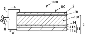
- the same reference numerals mean the same components (members). 1, 2, and 6 emphasize the size of the fine particles forming the porous layer 12. These fine particles are preferably clogged (deposited or adhered) in the horizontal and vertical directions with respect to the conductive support 11 to form a porous structure.
- the term “photoelectric conversion element 10” means the photoelectric conversion elements 10A to 10F unless otherwise specified.
- the simple term “photosensitive layer 13” means the photosensitive layers 13A to 13C unless otherwise specified.
- the hole transport layer 3 means the hole transport layers 3A and 3B unless otherwise specified.
- a system 100A shown in FIG. 1 is a system applied to a battery for causing an operation circuit M (for example, an electric motor) to perform work by the external circuit 6 using the photoelectric conversion element 10A.
- the photoelectric conversion element 10A includes a first electrode 1A, a second electrode 2, and a hole transport layer 3A.
- the first electrode 1A is porous as schematically shown in a conductive support 11 composed of a support 11a and a transparent electrode 11b, a porous layer 12, and an enlarged cross-sectional area a that is an enlarged cross-sectional area a in FIG.
- the surface of the material layer 12 has a photosensitive layer 13A provided with a perovskite light absorber. Further, the blocking layer 14 is provided on the transparent electrode 11 b, and the porous layer 12 is formed on the blocking layer 14. Thus, it is estimated that the photoelectric conversion element 10A having the porous layer 12 improves the charge separation and charge transfer efficiency because the surface area of the photosensitive layer 13A is increased.
- the photoelectric conversion element 10B shown in FIG. 2 schematically shows a preferred embodiment in which the photosensitive layer 13A of the photoelectric conversion element 10A shown in FIG. In the photoelectric conversion element 10B, the hole transport layer 3B is thinly provided.
- the photoelectric conversion element 10B differs from the photoelectric conversion element 10A shown in FIG. 1 in the film thicknesses of the photosensitive layer 13B and the hole transport layer 3B, but is configured in the same manner as the photoelectric conversion element 10A except for these points. ing.
- a photoelectric conversion element 10C shown in FIG. 3 schematically shows another preferred embodiment of the photoelectric conversion element of the present invention.
- the photoelectric conversion element 10C is different from the photoelectric conversion element 10B illustrated in FIG. 2 in that the porous layer 12 is not provided, but is configured in the same manner as the photoelectric conversion element 10B except for this point. That is, in the photoelectric conversion element 10 ⁇ / b> C, the photosensitive layer 13 ⁇ / b> C is formed in a thick film shape on the surface of the blocking layer 14. In the photoelectric conversion element 10 ⁇ / b> C, the hole transport layer 3 ⁇ / b> B can be provided thick like the hole transport layer 3 ⁇ / b> A.
- a photoelectric conversion element 10D shown in FIG. 4 schematically shows another preferred embodiment of the photoelectric conversion element of the present invention.
- This photoelectric conversion element 10D is different from the photoelectric conversion element 10C shown in FIG. 3 in that an electron transport layer 15 is provided instead of the blocking layer 14, but is otherwise configured in the same manner as the photoelectric conversion element 10C.
- the first electrode 1 ⁇ / b> D includes a conductive support 11 and an electron transport layer 15 and a photosensitive layer 13 ⁇ / b> C that are sequentially formed on the conductive support 11.
- This photoelectric conversion element 10D is preferable in that each layer can be formed of an organic material. As a result, the productivity of the photoelectric conversion element is improved, and it is possible to make it thinner or flexible.
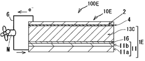
- a photoelectric conversion element 10E shown in FIG. 5 schematically shows still another preferred embodiment of the photoelectric conversion element of the present invention.
- a system 100E including the photoelectric conversion element 10E is a system applied to battery use as in the system 100A.
- the photoelectric conversion element 10 ⁇ / b> E has a first electrode 1 ⁇ / b> E, a second electrode 2, and an electron transport layer 4 between the first electrode 1 ⁇ / b> E and the second electrode 2.
- the first electrode 1 ⁇ / b> E includes a conductive support 11 and a hole transport layer 16 and a photosensitive layer 13 ⁇ / b> C, which are sequentially formed on the conductive support 11.
- This photoelectric conversion element 10E is preferable in that each layer can be formed of an organic material, like the photoelectric conversion element 10D.
- a photoelectric conversion element 10F shown in FIG. 6 schematically shows still another preferred embodiment of the photoelectric conversion element of the present invention.
- the photoelectric conversion element 10F is different from the photoelectric conversion element 10B illustrated in FIG. 2 in that the hole transport layer 3B is not provided, but is configured in the same manner as the photoelectric conversion element 10B except for this point.
- the system 100 to which the photoelectric conversion element 10 is applied functions as a solar cell as follows. That is, in the photoelectric conversion element 10, light that has passed through the conductive support 11 or passed through the second electrode 2 and entered the photosensitive layer 13 excites the light absorber. The excited light absorber has electrons with high energy and can emit these electrons. The light absorber that has released electrons with high energy becomes an oxidant.
- the photoelectric conversion elements 10A to 10D and 10F electrons emitted from the light absorber move between the light absorbers and reach the conductive support 11. After the electrons that have reached the conductive support 11 work in the external circuit 6, they pass through the second electrode 2 (if there is a hole transport layer 3, further via the hole transport layer 3), and then the photosensitive layer Return to 13. The light absorber is reduced by the electrons returning to the photosensitive layer 13.
- the photoelectric conversion element 10E the electrons emitted from the light absorber reach the second electrode 2 from the photosensitive layer 13C through the electron transport layer 4, and after working in the external circuit 6, the conductive support 11 Then, the process returns to the photosensitive layer 13. The light absorber is reduced by the electrons returning to the photosensitive layer 13.
- the system 100 functions as a solar cell by repeating such a cycle of excitation and electron transfer of the light absorber.
- the way in which electrons flow from the photosensitive layer 13 to the conductive support 11 differs depending on the presence and type of the porous layer 12 and the like.
- the porous layer 12 can be formed with an insulator other than the conventional semiconductor.
- the porous layer 12 is formed of a semiconductor, electron conduction in which electrons move inside or between the semiconductor particles of the porous layer 12 also occurs.
- the porous layer 12 is formed of an insulator, electron conduction in the porous layer 12 does not occur.
- a relatively high electromotive force can be obtained by using aluminum oxide (Al 2 O 3 ) particles as the insulator particles.
- Al 2 O 3 aluminum oxide
- the blocking layer 14 as the other layer is formed of a conductor or a semiconductor, electron conduction in the blocking layer 14 occurs. Electron conduction also occurs in the electron transport layer 15.
- the photoelectric conversion element and the solar cell of the present invention are not limited to the above-described preferred embodiments, and the configuration of each embodiment can be appropriately combined between the respective embodiments without departing from the spirit of the present invention.
- the photoelectric conversion element 10C or 10D may have a configuration in which the hole transport layer 3B is not provided as in the photoelectric conversion element 10F.
- the material and each member which are used for a photoelectric conversion element or a solar cell can be prepared by a conventional method except the material and member prescribed
- it can refer also about the material and each member which are used for a dye-sensitized solar cell.
- the dye-sensitized solar cell include Japanese Patent Application Laid-Open No. 2001-291534, US Pat. No. 4,927,721, US Pat. No. 4,684,537, US Pat. No. 5,0843,65.
- the first electrode 1 has a conductive support 11 and a photosensitive layer 13 and functions as a working electrode in the photoelectric conversion element 10. As shown in FIGS. 1 to 6, the first electrode 1 preferably has at least one of a porous layer 12, a blocking layer 14, an electron transport layer 15 and a hole transport layer 16. The first electrode 1 preferably has at least the blocking layer 14 in terms of prevention of short circuit, and more preferably has the porous layer 12 and the blocking layer 14 in terms of light absorption efficiency and prevention of short circuit. Moreover, it is preferable that the 1st electrode 1 has the electron transport layer 15 or the hole transport layer 16 formed with the organic material from the point of the improvement of productivity of a photoelectric conversion element, thickness reduction, or flexibility.
- the conductive support 11 is not particularly limited as long as it has conductivity and can support the photosensitive layer 13 and the like.
- the conductive support 11 includes a conductive material such as a metal, or a glass or plastic support 11a and a transparent electrode 11b as a conductive film formed on the surface of the support 11a. The structure which has is preferable.
- a conductive support 11 in which a transparent metal electrode 11b is formed by coating a conductive metal oxide on the surface of a glass or plastic support 11a is more preferable.
- the support 11a formed of plastic include a transparent polymer film described in paragraph No. 0153 of JP-A-2001-291534.
- ceramic Japanese Patent Laid-Open No. 2005-135902
- conductive resin Japanese Patent Laid-Open No. 2001-160425
- tin oxide As the metal oxide, tin oxide (TO) is preferable, and fluorine-doped tin oxide such as indium-tin oxide (tin-doped indium oxide; ITO) and fluorine-doped tin oxide (FTO) is particularly preferable.
- the coating amount of the metal oxide at this time is preferably 0.1 to 100 g per 1 m 2 of the surface area of the support 11a. When the conductive support 11 is used, light is preferably incident from the support 11a side.
- the conductive support 11 is substantially transparent.
- substantially transparent means that the transmittance of light (wavelength 300 to 1200 nm) is 10% or more, preferably 50% or more, and particularly preferably 80% or more.
- the thicknesses of the support 11a and the conductive support 11 are not particularly limited, and are set to appropriate thicknesses.
- the thickness is preferably 0.01 ⁇ m to 10 mm, more preferably 0.1 ⁇ m to 5 mm, and particularly preferably 0.3 ⁇ m to 4 mm.
- the film thickness of the transparent electrode 11b is not particularly limited, and is preferably 0.01 to 30 ⁇ m, more preferably 0.03 to 25 ⁇ m, and more preferably 0.05 to 20 ⁇ m. It is particularly preferred that
- the conductive support 11 or the support 11a may have a light management function on the surface.
- the surface of the conductive support 11 or the support 11a may have an antireflection film in which high refractive films and low refractive index oxide films are alternately stacked as described in JP-A-2003-123859.
- the light guide function described in JP-A-2002-260746 may be provided.
- a blocking layer 14 is provided.
- a photoelectric conversion element and a solar cell for example, when the photosensitive layer 13 or the hole transport layer 3 and the transparent electrode 11b are electrically connected, a reverse current is generated.
- the blocking layer 14 functions to prevent this reverse current.
- the blocking layer 14 is also referred to as a short circuit prevention layer.
- the blocking layer 14 can also function as a scaffold carrying the light absorber.
- This blocking layer 14 may also be provided when the photoelectric conversion element has an electron transport layer.
- the photoelectric conversion element 10D it may be provided between the conductive support 11 and the electron transport layer 15, and in the case of the photoelectric conversion element 10E, it is provided between the second electrode 2 and the electron transport layer 4. May be.
- the material for forming the blocking layer 14 is not particularly limited as long as it is a material capable of fulfilling the above functions, but is a substance that transmits visible light and is an insulating substance for the conductive support 11 (transparent electrode 11b) and the like. It is preferable that Specifically, the “insulating substance with respect to the conductive support 11 (transparent electrode 11b)” specifically refers to a material whose conduction band energy level forms the conductive support 11 (metal oxide forming the transparent electrode 11b). A compound (n-type semiconductor compound) that is higher than the energy level of the conduction band of the material and lower than the energy level of the conduction band of the material constituting the porous layer 12 and the ground state of the light absorber.
- Examples of the material for forming the blocking layer 14 include silicon oxide, magnesium oxide, aluminum oxide, calcium carbonate, cesium carbonate, polyvinyl alcohol, and polyurethane.
- the material generally used for the photoelectric conversion material may be used, and examples thereof include titanium oxide, tin oxide, zinc oxide, niobium oxide, and tungsten oxide. Of these, titanium oxide, tin oxide, magnesium oxide, aluminum oxide and the like are preferable.
- the thickness of the blocking layer 14 is preferably 0.001 to 10 ⁇ m, more preferably 0.005 to 1 ⁇ m, and particularly preferably 0.01 to 0.1 ⁇ m.
- the film thickness of each layer can be measured by observing the cross section of the photoelectric conversion element 10 using a scanning electron microscope (SEM) or the like.
- the porous layer 12 is preferably provided on the transparent electrode 11b.
- the blocking layer 14 is preferably formed on the blocking layer 14.
- the porous layer 12 is a layer that functions as a scaffold for carrying the photosensitive layer 13 on the surface.
- the porous layer 12 is preferably a fine particle layer having pores, in which fine particles of the material forming the porous layer 12 are deposited or adhered.
- the porous layer 12 may be a fine particle layer in which two or more kinds of fine particles are deposited.
- the amount of light absorbent supported (adsorption amount) can be increased.
- the surface area of the porous layer 12 it is preferable to increase the surface area of the individual fine particles constituting the porous layer 12.
- the surface area of the fine particles is preferably 10 times or more, more than 100 times the projected area. It is more preferable.
- the particle diameter of the fine particles forming the porous layer 12 is preferably 0.001 to 1 ⁇ m as the primary particle in the average particle diameter using the diameter when the projected area is converted into a circle.
- the average particle diameter of the fine particles is preferably 0.01 to 100 ⁇ m as the average particle diameter of the dispersion.
- the material for forming the porous layer 12 is not particularly limited with respect to conductivity, and may be an insulator (insulating material), a conductive material, or a semiconductor (semiconductive material).
- Examples of the material for forming the porous layer 12 include metal chalcogenides (eg, oxides, sulfides, selenides, etc.), compounds having a perovskite crystal structure (excluding perovskite compounds used as a light absorber), silicon. These oxides (for example, silicon dioxide, zeolite) or carbon nanotubes (including carbon nanowires and carbon nanorods) can be used.
- the metal chalcogenide is not particularly limited, but is preferably titanium, tin, zinc, tungsten, zirconium, hafnium, strontium, indium, cerium, yttrium, lanthanum, vanadium, niobium, aluminum or tantalum oxide, cadmium sulfide. , Cadmium selenide and the like.
- Examples of the crystal structure of the metal chalcogenide include an anatase type, brookite type and rutile type, and anatase type and brookite type are preferable.
- the compound having a perovskite crystal structure is not particularly limited, and examples thereof include transition metal oxides.
- transition metal oxides For example, strontium titanate, calcium titanate, barium titanate, lead titanate, barium zirconate, barium stannate, lead zirconate, strontium zirconate, strontium tantalate, potassium niobate, bismuth ferrate, strontium barium titanate , Barium lanthanum titanate, calcium titanate, sodium titanate, bismuth titanate.
- strontium titanate, calcium titanate and the like are preferable.
- the carbon nanotube has a shape obtained by rounding a carbon film (graphene sheet) into a cylindrical shape.
- Carbon nanotubes are single-walled carbon nanotubes (SWCNT) in which one graphene sheet is wound in a cylindrical shape, double-walled carbon nanotubes (DWCNT) in which two graphene sheets are wound in a concentric shape, and multiple graphene sheets are concentric
- SWCNT single-walled carbon nanotubes
- DWCNT double-walled carbon nanotubes
- MWCNT multi-walled carbon nanotubes
- any carbon nanotube is not particularly limited and can be used.
- the material for forming the porous layer 12 is preferably titanium, tin, zinc, zirconium, aluminum or silicon oxide, or carbon nanotube, more preferably titanium oxide or aluminum oxide.
- the porous layer 12 may be formed of at least one of the above-described metal chalcogenide, compound having a perovskite crystal structure, silicon oxide, and carbon nanotube, and may be formed of a plurality of types. .
- the thickness of the porous layer 12 is not particularly limited, but is usually in the range of 0.05 to 100 ⁇ m, preferably in the range of 0.1 to 100 ⁇ m. When used as a solar cell, the thickness is preferably 0.1 to 50 ⁇ m, more preferably 0.2 to 30 ⁇ m, and still more preferably 0.3 to 30 ⁇ m.
- the electron transport layer 15 is preferably provided on the surface of the transparent electrode 11b.
- the electron transport layer 15 has a function of transporting electrons generated in the photosensitive layer 13 to the conductive support 11.
- the electron transport layer 15 is formed of an electron transport material that can exhibit this function.
- the electron transport material is not particularly limited, but an organic material (organic electron transport material) is preferable.
- the organic electron transport material examples include fullerene compounds such as [6,6] -Phenyl-C61-Butylic Acid Methyl Ester (PC 61 BM), perylene compounds such as perylene tetracarboxydiimide (PTCDI), and other tetracyanoquinodimethanes. Examples thereof include a low molecular compound such as (TCNQ) or a high molecular compound.
- the thickness of the electron transport layer 15 is not particularly limited, but is preferably 0.001 to 10 ⁇ m, and more preferably 0.01 to 1 ⁇ m.
- the hole transport layer 16 is preferably provided on the surface of the transparent electrode 11b.
- the hole transport layer 16 is the same as the hole transport layer 3 described later except that the position where it is formed is different.
- the photosensitive layer 13 has a perovskite crystal structure having an organic cation represented by the above formula (IA), a cation of a metal atom, and an anion of an anionic atom or atomic group.
- a porous layer 12 photoelectric conversion elements 10A, 10B and 10F
- a blocking layer 14 photoelectric conversion element 10C
- an electron transport layer 15 photoelectric conversion element 10D
- It is provided on the surface of each layer of the hole transport layer 16 (photoelectric conversion element 10E) (including the inner surface of the recess when the surface on which the photosensitive layer 13 is provided is uneven).
- the light absorber only needs to contain at least one of the specific perovskite compounds, and may contain two or more perovskite compounds.
- the light absorber may contain a light absorber other than the perovskite compound in combination with the perovskite compound.
- Examples of the light absorber other than the perovskite compound include metal complex dyes and organic dyes.
- the ratio of the perovskite compound to other light absorbers is not particularly limited.
- the photosensitive layer 13 may be a single layer or a laminate of two or more layers.
- the photosensitive layer 13 may be a laminated structure in which layers made of different light absorbers are laminated, and an intermediate including a hole transport material between the photosensitive layer and the photosensitive layer.
- a laminated structure having layers may also be used.
- the form that the photosensitive layer 13 can take is as described above.
- the photosensitive layer 13 is preferably provided on the surface of the porous layer 12 or the blocking layer 14 so that electrons excited on the conductive support 11 flow. At this time, the photosensitive layer 13 may be provided on the entire surface, or may be provided on a part of the surface. When the porous layer 12 is used, the photosensitive layer 13 is provided inside the pores of the porous layer 12. May be.
- the film thickness of the photosensitive layer 13 is appropriately set according to the form that the photosensitive layer can take, and is not particularly limited.
- the film thickness of the photosensitive layer 13 is, for example, preferably 0.001 to 100 ⁇ m, more preferably 0.01 to 10 ⁇ m, and particularly preferably 0.01 to 5 ⁇ m.
- the total film thickness with the porous layer 12 is preferably 0.01 ⁇ m or more, more preferably 0.05 ⁇ m or more, further preferably 0.1 ⁇ m or more, and 0.2 ⁇ m or more. Particularly preferred.
- the total film thickness is preferably 100 ⁇ m or less, more preferably 50 ⁇ m or less, further preferably 30 ⁇ m or less, and particularly preferably 3 ⁇ m or less.
- the total film thickness can be in a range where the above values are appropriately combined.
- the total film thickness with the porous layer 12 is preferably 0.1 to 100 ⁇ m, more preferably 0.1 to 50 ⁇ m, and particularly preferably 0.2 to 3 ⁇ m.
- the film thickness of the photosensitive layer 13 is the interface with the porous layer 12 along the direction perpendicular to the surface of the porous layer 12. This is the distance from the interface with the hole transport layer 3 described later.
- the total film thickness of the porous layer 12, the photosensitive layer 13, and the hole transport layer 3 is not particularly limited, but is preferably 0.01 ⁇ m or more, more preferably 0.05 ⁇ m or more, and 0 .1 ⁇ m or more is more preferable, and 0.3 ⁇ m or more is particularly preferable.
- the total film thickness is preferably 200 ⁇ m or less, more preferably 50 ⁇ m or less, further preferably 30 ⁇ m or less, and particularly preferably 5 ⁇ m or less.
- the total film thickness can be in a range where the above values are appropriately combined.
- the thickness of the photosensitive layer is larger than that of the photosensitive layer shown in FIG. 1, but the perovskite type light absorber represented by the formula (I) used in the present invention is different from other perovskite types. Like a compound, it can be a hole transport material.
- the perovskite type light absorber may be used in an amount that covers at least a part of the surface of the porous layer 12 or the blocking layer 14 where light is incident, and is preferably an amount that covers the entire surface.
- the content of the perovskite compound is usually 1 to 100% by mass.
- the photosensitive layer 13 contains at least one perovskite compound having a cationic organic group, a metal atom, and an anionic atom or atomic group as a light absorber.
- the cationic organic group, metal atom, and anionic atom or atomic group of the perovskite compound are respectively an organic cation (sometimes referred to as an organic cation A for convenience) and a metal cation (referred to as a cation M for convenience).
- anion sometimes referred to as anion X for convenience).
- the cationic organic group means an organic group having a property of becoming an organic cation in a perovskite crystal structure
- the anionic atom or atomic group is an atom or atom having a property of becoming an anion in a perovskite crystal structure.
- the perovskite compound used in the present invention is a compound having a perovskite crystal structure having an organic cation represented by the following formula (IA), a cation of a metal atom, and an anion of an anionic atom or atomic group.
- RA represents an alkyl group, a cycloalkyl group, an alkenyl group, an alkynyl group, an aryl group, a heteroaryl group, or a group that can be represented by the following formula (2).
- R B represents NR 1 R 2 or (NR 1 R 2 R 3 ) + , and R 1 , R 2 and R 3 each independently represent a hydrogen atom or a substituent.
- L represents a linking group.
- n2 represents an integer of 1 or more. However, (R B ) n2 -L is a group different from R A. n represents a number satisfying 0 ⁇ n ⁇ 1.00.
- Xa represents NR ⁇ 1c> , an oxygen atom, or a sulfur atom.
- R 1b and R 1c each independently represent a hydrogen atom or a substituent.
- *** represents a bond with the nitrogen atom of formula (IA).
- the reason why the variation in wet heat durability can be reduced is as follows. Although not sure yet, it is estimated as follows. That is, in the perovskite compound, when two different organic ammonium cations, ie, an organic ammonium cation having one amino group and an organic ammonium cation having two or more amino groups, are used, the organic ammonium cation having one amino group is used.
- the perovskite crystal structure is stabilized by the amino group of the ammonium cation having two or more amino groups, and defects in the crystal lattice are less likely to occur.
- the interface state with the layer adjacent to the photosensitive layer 13 becomes uniform, and the deterioration in performance caused by moisture or heat under high temperature and high humidity occurs on the interface or in the crystal. It is considered that the variation was reduced by always relaxing a certain part with a certain effect.
- defective crystal parts are greatly affected by the deterioration of performance due to moisture and heat entering the interior due to being placed under high temperature and high humidity, and the fact that the number of defects is reduced by the present invention itself is considered to be the reason why variation can be reduced. It is done.
- the excellent photoelectric conversion efficiency exhibited by the organic ammonium cation having one amino group is not lowered by the presence of an ammonium cation having two or more amino groups, and the battery performance of the perovskite sensitized solar cell is maintained. .
- the light absorber used in the present invention two kinds of cations represented by the above formula (IA) are used in combination as the organic cation constituting the perovskite crystal structure. That is, one is [R A —NH 2 (H + )] and the other is ⁇ [(R B ) n2 —L—NH 2 ] (H + ) ⁇ .
- the perovskite compound only needs to have the two organic cations as the entire light absorber.
- the perovskite compound may be a perovskite compound having two organic cations, a perovskite compound having [R A —NH 2 (H + )], and ⁇ [(R B ) n2 -L—NH 2 ]. It may be a mixture with a perovskite compound having (H + ) ⁇ .
- the organic cation represented by [R A —NH 2 (H + )] is an ammonium cation formed by combining R A and NH 2 in the above formula (IA).
- An organic ammonium cation (R A —NH 3 + ) composed of a reactive organic group A is preferred.
- the organic ammonium cation can take a resonance structure
- the organic cation includes a cation having a resonance structure in addition to the organic ammonium cation.
- the organic cation is bonded to the group that can be represented by the above formula (2) and NH 2.
- an organic amidinium cation which is one of the resonance structures of the organic ammonium cation is also included.
- Examples of the organic amidinium cation comprising an amidinium cationic organic group include a cation represented by the following formula (A am ).
- a cation represented by the following formula (A am ) may be represented as “R 1b C ( ⁇ NH) —NH 3 ” for convenience.
- the alkyl group as R A in formula (IA) may be an unsubstituted alkyl group having no substituent or a substituted alkyl group having a substituent.
- the unsubstituted alkyl group is also a linear alkyl group and is not particularly limited, but is preferably an alkyl group having 1 to 18 carbon atoms, more preferably an alkyl group having 1 to 6 carbon atoms, and an alkyl group having 1 to 3 carbon atoms. More preferred are groups. Examples of such an alkyl group include methyl, ethyl, n-propyl, n-butyl, n-pentyl, n-hexyl, n-decyl and the like.
- the substituted alkyl group is not particularly limited as long as the above-described unsubstituted alkyl group has a substituent T described later, and may be linear or branched.
- the unsubstituted alkyl group before the substituted alkyl group is substituted with the substituent T may be the above-mentioned unsubstituted alkyl group, preferably an alkyl group having 1 to 4 carbon atoms, more preferably 1 to carbon atoms. 3 alkyl group, and more preferably an alkyl group having 1 or 2 carbon atoms.
- the cycloalkyl group is preferably a cycloalkyl group having 3 to 8 carbon atoms, and examples thereof include cyclopropyl, cyclopentyl, and cyclohexyl.
- the alkenyl group may be linear or branched and is preferably an alkenyl group having 2 to 18 carbon atoms, more preferably an alkenyl group having 2 to 6 carbon atoms.
- alkenyl group having 2 to 18 carbon atoms
- alkenyl group having 2 to 6 carbon atoms For example, ethenyl, allyl, butenyl, hexenyl and the like can be mentioned.
- Examples of the branched alkenyl group include 1-methyl-2-propenyl.
- the alkynyl group is preferably an alkynyl group having 2 to 18 carbon atoms, more preferably an alkynyl group having 2 to 4 carbon atoms, and examples thereof include ethynyl, butynyl and hexynyl.
- the aryl group is preferably an aryl group having 6 to 14 carbon atoms, more preferably an aryl group having 6 to 12 carbon atoms, and examples thereof include phenyl.
- the heteroaryl group includes a group consisting only of an aromatic heterocycle and a group consisting of a condensed heterocycle obtained by condensing an aromatic heterocycle with another ring such as an aromatic ring, an aliphatic ring or a heterocycle.
- a ring-constituting hetero atom constituting the aromatic hetero ring a nitrogen atom, an oxygen atom and a sulfur atom are preferable.
- the number of ring members of the aromatic heterocycle is preferably a 3- to 8-membered ring, and more preferably a 5-membered ring or a 6-membered ring.
- the condensed heterocycle including a 5-membered aromatic heterocycle and a 5-membered aromatic heterocycle include a pyrrole ring, an imidazole ring, a pyrazole ring, an oxazole ring, a thiazole ring, a triazole ring, a furan ring, and a thiophene ring. , Benzimidazole ring, benzoxazole ring, benzothiazole ring, indoline ring, and indazole ring.
- Examples of the condensed heterocycle including a 6-membered aromatic heterocycle and a 6-membered aromatic heterocycle include, for example, pyridine ring, pyrimidine ring, pyrazine ring, triazine ring, quinoline ring, and quinazoline ring. Is mentioned.
- X a represents NR 1c , an oxygen atom or a sulfur atom, and NR 1c is preferable.
- R 1c represents a hydrogen atom or a substituent, and is preferably a hydrogen atom, an alkyl group, a cycloalkyl group, an alkenyl group, an alkynyl group, an aryl group or a heteroaryl group, and more preferably a hydrogen atom.
- R 1b represents a hydrogen atom or a substituent, and preferably a hydrogen atom.
- R 1b examples include an alkyl group, a cycloalkyl group, an alkenyl group, an alkynyl group, an aryl group, a heteroaryl group, and an amino group.
- An alkyl group, a cycloalkyl group, an alkenyl group, an alkynyl group, an aryl group and a heteroaryl group, which can be adopted as R 1b and R 1c have the same meanings as those of the above-mentioned groups of RA , and preferred ones are also the same.
- Examples of the group that can be represented by the formula (2) include a (thio) acyl group, a (thio) carbamoyl group, an imidoyl group, and an amidino group.
- the (thio) acyl group includes an acyl group and a thioacyl group.
- the acyl group is preferably an acyl group having 1 to 7 carbon atoms, and examples thereof include formyl, acetyl, propionyl, hexanoyl and the like.
- the thioacyl group is preferably a thioacyl group having 1 to 7 carbon atoms in total, and examples thereof include thioformyl, thioacetyl, thiopropionyl and the like.
- the (thio) carbamoyl group includes a carbamoyl group and a thiocarbamoyl group.
- the amidino group as a group that can be represented by the formula (2) has a structure in which R 1b of the imidoyl group is an amino group and R 1c is a hydrogen atom.
- each group of RA may have is not particularly limited as long as it is a group other than an amino group and a substituted amino group. That is, R A which may have a substituent is different from “(R B ) n2 -L” of another cation described later.
- the substituted amino group includes, for example, a mono- or di-alkylamino group (including a nitrogen-containing aliphatic heterocycle), a mono- or di-arylamino group, an acylamino group, a sulfonamide group, a carbamoyl group, a sulfamoyl group, and the like. Can be mentioned.
- the following substituent T is mentioned as a substituent which each group of RA may have.
- the substituent T is not particularly limited, and examples thereof include an alkyl group, a cycloalkyl group, an alkenyl group, an alkynyl group, an aryl group, a heteroaryl group, an alkoxy group, an alkylthio group, an acyl group, an alkoxycarbonyl group, an alkylcarbonyloxy group, An aryloxycarbonyl group, an aryloxy group, an arylcarbonyloxy group, a halogen atom, a cyano group, a hydroxy group, a mercapto group or a carboxy group can be mentioned.
- R A is a methyl group
- the substituent T does not include an imino ( ⁇ NH) group.
- the substituent T is more preferably an alkyl group, a halogen atom, a cyano group, an aryl group, or a group obtained by combining these, and a halogen atom is particularly preferable.
- an alkyl group, a cycloalkyl group, an alkenyl group, an alkynyl group and an aryl group have the same meaning as the alkyl group, cycloalkyl group, alkenyl group, alkynyl group and aryl group of the above R A , and preferred ones Is the same.
- the heteroaryl group has the same meaning as the heteroaryl group of R A , but a heteroaryl group that does not contain a nitrogen atom as a ring atom is preferable.
- Each of the alkoxy group and the alkylthio group is preferably an alkyl group in which the alkyl portion is the same as the alkyl group of the above RA .
- the acyl group, alkoxycarbonyl group, and alkylcarbonyloxy group each preferably have the same alkyl moiety as the alkyl group of RA above.
- the aryloxycarbonyl group, aryloxy group, and arylcarbonyloxy group each preferably have the same aryl group or heteroaryl group as the aryl group of R A described above.
- the halogen atom is preferably a fluorine atom, a chlorine atom, a bromine atom or an iodine atom, more preferably a fluorine atom, a chlorine atom or a bromine atom, and particularly preferably a fluorine atom.
- each substituent may be further substituted with a substituent.
- the group is not particularly limited as long as it is a group obtained by combining at least two kinds of the above-described substituents. ), A cyanoalkyl group, and the like.
- each substituent T may be the same as or different from each other. Moreover, when several substituent T adjoins (especially when adjoining), they may mutually connect and a ring may be formed.
- a ring for example, an alicyclic ring, an aromatic ring, or a heterocyclic ring, may form a condensed ring in which these are condensed.
- R A is preferably a substituted alkyl group, an unsubstituted alkyl group, an aryl group, a heteroaryl group, or a group that can be represented by the formula (2) among the above-mentioned groups in that variation in photoelectric conversion efficiency can be reduced.
- a substituted alkyl group, an unsubstituted alkyl group, or a group that can be represented by formula (2) is more preferred, an alkyl group that is substituted with a halogen atom or a group that can be represented by formula (2) is more preferred, and a fluorine atom is substituted.
- Particularly preferred are alkyl groups.
- RA and NH 2 or NH 3 + become one of the organic cations.
- the following r-1 to r-23 are shown as specific examples of R A below, but the present invention is not limited thereto.
- “*” represents a bond with a nitrogen atom
- “Me” represents a methyl group
- “Et” represents an ethyl group.
- R B represents an amino group or a substituted amino group or a cation thereof, and specifically represents NR 1 R 2 or (NR 1 R 2 R 3 ) + .
- R 1 , R 2 and R 3 are each independently a hydrogen atom or a substituent.
- R 1 , R 2 and R 3 are each preferably a hydrogen atom from the viewpoint that the perovskite crystal structure can be stabilized and variation in wet heat durability can be kept small.
- R 1 , R 2 or R 3 is a substituent, the substituent is not particularly limited, and examples thereof include the above-described substituent T, and the preferable one is the same, and an alkyl group is particularly preferable.
- the cation may have a counter anion Y B- .
- the counter anion Y B- is not particularly limited, and various anions can be mentioned. Examples of the anion include halide ions (F ⁇ , I ⁇ , Br ⁇ , Cl ⁇ and the like), OH ⁇ , CF 3 SO 3 ⁇ , CH 3 COO ⁇ , SH ⁇ , SCN ⁇ , ClO 4 ⁇ and the like. Of these, halide ions are preferable, and I ⁇ is more preferable.
- Y B- may be incorporated into the perovskite structure represented by the adjacent formula (I).
- L is a linking group, and preferably has at least one group selected from the group consisting of groups represented by the following formulas L-1 to L-9.
- the linking group L has at least one group selected from the group consisting of groups represented by the formulas L-1 to L-9 means that the linking group L has the following formulas L-1 to L-9 A group formed by combining at least two groups selected from the group consisting of groups represented by the following formulas L-1 to L-9 with a group represented by any one of L-9 Including the case of
- R 4 and R 5 are each independently a hydrogen atom or a substituent, and each is preferably a hydrogen atom.
- substituents include the above-described substituent T, preferably an alkyl group and a halogen atom.
- the alkyl group is synonymous with the alkyl group of RA , and the preferred one is the same, but methyl is particularly preferred.
- D 1 represents a nitrogen atom or CR 10 .
- R 10 represents a hydrogen atom or a substituent, and preferably a hydrogen atom.
- substituents include the above-described substituent T, preferably an alkyl group, an alkenyl group, an alkynyl group, an aryl group, a heteroaryl group, and a halogen atom, and more preferably an alkyl group.
- the alkyl group has the same meaning as the alkyl group for RA , but is preferably an alkyl group having 1 to 30 carbon atoms, and more preferably an alkyl group having 1 to 10 carbon atoms.
- R 6 and R 7 are each independently a hydrogen atom or a substituent. When R 6 and R 7 are substituents, they may be the same or different substituents.
- the substituent for R 6 and R 7 is preferably as defined for the above substituent T, and among them, an alkyl group, a cyano group, and a halogen atom are preferable.
- the above formula L-4 is represented as a trans isomer, but may be a cis isomer.
- D 2 represents an oxygen atom, a sulfur atom or NR 11 .
- R 11 has the same meaning as R 10 , and preferred ones are also the same.
- E represents an oxygen atom, a sulfur atom or NR 12 .
- R 12 has the same meaning as R 10 , and preferred ones are also the same.
- R 8 represents a substituent, and has the same meaning as that of the substituent of R 10 , and preferred examples thereof are also the same.
- m1 represents an integer of 0 or more, preferably an integer of 0 to 2, and more preferably 0.
- m2 represents an integer of 0 or more, preferably an integer of 0 to 3, and more preferably 0 (5-membered ring) or 1 (6-membered ring).
- m3 represents an integer of 2 or more, preferably an integer of 2 to 5, and more preferably 3 or 4.
- the ring G represents an aryl ring composed of a carbon atom group necessary for constituting the ring, or a heteroaryl ring composed of the above carbon atom group and Z 1 .
- Z 1 represents a hetero atom or NR 13 .
- the hetero atom include a nitrogen atom, an oxygen atom, and a sulfur atom, and a nitrogen atom or a sulfur atom is preferable.
- R 13 has the same meaning as R 10 , and preferred ones are also the same.
- R 9 represents a substituent, has the same meaning as R 8 , and preferred ones are also the same.
- m4 represents an integer of 0 or more, preferably an integer of 0 to 3, and more preferably 0.
- n5 represents an integer of 0 or more, preferably an integer of 0 to 3, and more preferably 0 (aryl ring) or 1 (heteroaryl ring).
- m6 represents an integer of 2 or more, preferably an integer of 2 to 5, and more preferably 3 or 4.
- the group represented by the formula L-8 is preferably a group represented by the following formula L-10, and the group represented by the formula L-9 is a group represented by the following formula L-11. Is preferred.
- * represents a connecting position with R B , NH 2 or a group represented by the above formula.
- m7 represents an integer of 0 or more, and is synonymous with m2 in the formula L-8, and preferred examples thereof are also the same.
- m8 represents an integer of 3 or more, preferably an integer of 3 to 5, and more preferably 3 or 4.
- Z 1 has the same meaning as Z 1 of the formula L-9, it is preferable also the same.
- m5 represents an integer of 0 or more, and is synonymous with m5 in Formula L-9, and preferred examples are also the same.
- m9 represents an integer of 3 or more, preferably an integer of 3 to 5, and more preferably 3 or 4.
- Ring G represented by formula L-9 and formula L-11 is not particularly limited, but is an aryl ring such as a benzene ring, pyrrole ring, thiophene ring, furan ring, imidazole ring, pyrazole ring, oxazole ring, Examples include a heteroaryl ring such as a thiazole ring, an oxadiazole ring, a thiadiazole ring, an isoxazole ring, an isothiazole ring, a triazole ring, a pyridine ring, a pyrazine ring, a pyrimidine ring, a pyridazine ring, and a triazine ring.
- a pyridine ring or a triazine ring is preferable, and a thiophene ring is more preferable.
- the linking group L is a group formed by combining at least two groups selected from the group consisting of the groups represented by the formulas L-1 to L-9
- the type of group to be combined is particularly It is not limited, A plurality of the same kind of groups may be combined, or all different groups may be combined. In this case, at least two groups selected from the group consisting of the groups represented by the above formulas L-1 to L-9 may be linked to form a ring structure.
- the number of groups to be combined is not particularly limited, and is preferably 2 to 50, for example, and more preferably 2 to 10.
- the chain length of the combined linking group is preferably from 0 to 10, more preferably from 0 to 5.
- the length of the chain of the linking group is the minimum number of atoms constituting a chain between atoms bonded to two amino groups. In the case of having 3 or more amino groups (when there are 3 or more linking positions *), the chain length of each combination of two amino groups is determined, and the largest of these is determined. For example, the minimum number of atoms between two amino groups of the following compound L-2-2 is 5 and the chain length of the linking group is 5.
- the minimum number of atoms between two amino groups of compound L-8-4 is all 3, and the chain length of the linking group is 3.
- the minimum number of atoms between the two amino groups of compound L-9-4 is 2, 3 and 4, and the chain length of the linking group is 4.
- a group formed by combining at least two groups selected from the group consisting of groups represented by formula L-1 to formula L-9 is represented by any one of formulas Lp-1 to Lp-9 below. It is preferably a group.
- R 4 and R 5 have the same meanings as R 4 and R 5 of the group represented by the formula L-1, respectively, and preferred ones are also the same.
- p represents an integer of 2 or more, preferably an integer of 2 to 5, and more preferably 2.
- L p1 represents a single bond or a group represented by the formula Lp-1, and at least one of the plurality of L p1 Is a group represented by the above formula Lp-1, and a plurality of L p1 may be the same or different.
- D 1 has the same meaning as D 1 of the group represented by the formula L-2, and preferred ones are also the same.
- R 6 and R 7 have the same meanings as R 6 and R 7 in the group represented by the formula L-4, respectively, and preferred examples thereof are also the same.
- D 2 has the same meaning as D 2 of the group represented by the formula L-6, and preferred ones are also the same.
- E has the same meaning as E in the group represented by the formula L-7, and the preferable ones are also the same, and two Es may be the same as or different from each other.
- D 2 has the same meaning as D 2 of the group represented by Formula L-6, and preferred ones are also the same.
- R 8 , m1, m2 and m3 are the same as R 8 , m1, m2 and m3 of the group represented by the formula L-8, respectively, and preferred ones are also the same.
- the group formed by the combination is more preferably a group formed by the following combination.
- a group represented by the above formula Lp-1 comprising a combination of a plurality of, preferably 2 to 5, more preferably two groups represented by the formula L-1 (having this group, [(R B ) As amine compounds represented by n2 -L-NH 2 ], for example, the following compounds L-1-1 to L-1-4),
- a group consisting of a combination of one or more groups represented by formula L-3 and one or more groups represented by formula L-1 preferably one group represented by formula L-3 and 4 Examples of the group represented by the above formula Lp-3 consisting of a group represented
- the linking group L has at least one selected from the group consisting of groups represented by formula L-1, formula L-2, formula L-3, formula L-8 and formula L-9. However, it is preferable in that the variation in wet heat durability can be suppressed small. More preferably, it has at least one selected from the group consisting of groups represented by formula L-1, formula L-2, formula L-3, formula L-10, and formula L-11.
- the linking group L more preferably has at least one group selected from the group consisting of groups represented by formula L-2, formula L-3, formula L-10 and formula L-11. Particularly preferably, a group represented by the formula Lp-1, a group represented by the formula Lp-2, a group represented by the formula Lp-3, a group represented by the formula L-10, a group represented by the formula L-11 Group.
- the linking group L preferably has a symmetric structure.
- the symmetry structure may be any of line symmetry, point symmetry, rotational symmetry, and the like.
- the plurality of L p1 are preferably the same.
- n2 represents an integer of 1 or more, preferably an integer of 1 to 5, and more preferably 2 or 3.
- n2 is within the above range, the stability of the perovskite crystal is improved, and variation in wet heat durability can be suppressed to a low level.
- amine compound represented by [(R B ) n2 -L-NH 2 ] in the formula (IA) are shown below, but the present invention is not limited thereto.
- Compound No. “NL” in “L-nL-mL” represents a number corresponding to Formula L-1 to Formula L-9 or Formula Lp-1 to Formula Lp-9, and “mL” represents the number of the exemplified compound in each formula.
- the linking group L in the following compound is a residue obtained by removing all amino groups (excluding those corresponding to the above D 1 , D 2 and E) from the following compound.
- n represents a number satisfying 0 ⁇ n ⁇ 1.00, preferably a number satisfying 0.05 ⁇ n ⁇ 0.90, more preferably 0.10 ⁇ n ⁇ It is a number that satisfies 0.50, and more preferably a number that satisfies 0.15 ⁇ n ⁇ 0.30.
- the above n is determined by the composition ratio (molar ratio) of the synthetic raw material of the perovskite type light absorber.
- the perovskite compound used in the present invention has a metal atom cation (metal cation) in its crystal structure.
- the metal cation is not particularly limited as long as it is a metal atom cation capable of having a perovskite crystal structure.
- metal atoms include calcium (Ca), strontium (Sr), cadmium (Cd), copper (Cu), nickel (Ni), manganese (Mn), iron (Fe), cobalt (Co), Metal atoms such as palladium (Pd), germanium (Ge), tin (Sn), lead (Pb), ytterbium (Yb), europium (Eu), indium (In), and the like can be given.
- the metal cation is particularly preferably a Pb atom or a Sn atom cation.
- the metal cation may be one type or two or more types. In the case of two or more kinds of metal cations, two kinds of cations of Pb atom and Sn atom are preferable.
- the ratio of the metal cation at this time is not particularly limited.
- the perovskite compound used in the present invention has an anion in its crystal structure.
- the anion is preferably an anionic atom such as a halogen atom, or each anion of an anionic atomic group of NCS ⁇ , NCO ⁇ , CH 3 COO ⁇ or HCOO ⁇ .
- a halogen atom anion is more preferable.
- a fluorine atom, a chlorine atom, a bromine atom, an iodine atom, etc. are mentioned, for example.
- the anion may be an anion of one kind of atom or atomic group, or may be an anion of two or more kinds of atoms or atomic groups.
- an anion of iodine atom is preferable.
- there are two or more anions those represented by the following formula (x) are preferred.
- X A1 and X A2 each independently represent an anion different from each other, preferably an anions having different halogen atoms, one being an anion having an iodine atom, and the other being an anion having a chlorine atom or a bromine atom More preferably, it is an anion.
- m is preferably 0.01 to 2.99, more preferably 0.1 to 1.4, and still more preferably 0.5 to 1.0.
- the perovskite compound having each constituent ion described above may be a compound that can have a perovskite crystal structure including each constituent ion, and is preferably a perovskite compound represented by the following formula (I).
- A represents a cationic organic group.
- M represents a metal atom.
- X represents an anionic atom or atomic group.
- a represents 1 or 2
- the cationic organic group represented by A forms an organic cation represented by the above formula (IA) in the perovskite crystal structure. Therefore, the cationic organic group has the same meaning as R A —NH 2 and [(R B ) n2 -L—NH 2 ] in the above formula (IA) described above for the organic cation, and preferable ones are also the same. is there.
- R A , R B , n2 and L are as described above.
- the metal atom represented by M is a metal atom that forms the metal cation in the perovskite crystal structure. Such a metal atom is synonymous with the metal atom demonstrated by the said metal cation, and a preferable thing is also the same.
- the anionic atom or atomic group represented by X is an anionic atom or atomic group forming the anion in the perovskite crystal structure.
- Such an anionic atom or atomic group is synonymous with the anionic atom or atomic group described in the above anion, and preferred ones are also the same.
- the perovskite compound represented by formula (I) is a perovskite compound represented by the following formula (I-1) when a is 1, and when a is 2, the perovskite compound represented by formula (I-2) It is a perovskite compound represented.
- A represents a cationic organic group and has the same meaning as A in the formula (I), and the preferred ones are also the same.
- M represents a metal atom and is synonymous with M in the above formula (I), and preferred ones are also the same.
- X represents an anionic atom or an atomic group, and is synonymous with X in the formula (I), and preferred ones are also the same.
- the perovskite compound used in the present invention may be either a compound represented by formula (I-1) or a compound represented by formula (I-2), or a mixture thereof. Therefore, in the present invention, at least one perovskite compound only needs to be present as a light absorber, and it is not necessary to clearly distinguish which compound is strictly based on the composition formula, molecular formula, crystal structure, and the like. .
- the method for producing the perovskite light absorber used in the present invention is not particularly limited, and can be synthesized according to a known method using R A —NH 2 and (R B ) n2 —L—NH 2 .
- Known methods include, for example, the methods described in Patent Documents 1 and 2 and Non-Patent Document 1.
- the method described in 6050-6051 is also included.
- perovskite type represented by the formula (I) using MX 2 and R A —NH 3 X, (R B ) n2 -L—NH 3 X and MX 2 Light absorbers can be synthesized.
- X represents an atom or atomic group to be an anion, and has the same meaning as X in the above formula (I).
- R A has the same meaning as R A in the above formula (IA)
- R B is L and n2 have the same meanings as R B, L and n2 in each of the aforementioned formula (IA).
- the molar ratio of MX 2 to R A —NH 3 X and (R B ) n2 —L—NH 3 X is adjusted in accordance with n in formula (IA).
- the hole transport layer 3 is provided between the first electrode 1 and the second electrode 2 as in the photoelectric conversion elements 10A to 10D.
- the hole transport layer 3 is preferably provided between the photosensitive layer 13 of the first electrode 1 and the second electrode 2.
- the hole transport layer 3 has a function of replenishing electrons to the oxidant of the light absorber, and is preferably a solid layer (solid hole transport layer).
- the hole transport material forming the hole transport layer 3 may be a liquid material or a solid material, and is not particularly limited. Examples thereof include inorganic materials such as CuI and CuNCS, and organic hole transport materials described in paragraph numbers 0209 to 0212 of JP-A No. 2001-291534, for example.
- the organic hole transport material is preferably a conductive polymer such as polythiophene, polyaniline, polypyrrole and polysilane, a spiro compound in which two rings share a tetrahedral structure such as C and Si, and triarylamine. And aromatic amine compounds such as triphenylene compounds, nitrogen-containing heterocyclic compounds, and liquid crystalline cyano compounds.
- the hole transporting material is preferably an organic hole transporting material that can be applied by solution and becomes solid.
- 2,2 ′, 7,7′-tetrakis- (N, N-di-p-methoxyphenyl) Amine) -9,9-spirobifluorene also referred to as spiro-OMeTAD
- 4- (diethylamino) benzaldehyde diphenylhydrazone
- PEDOT polyethylenedioxythiophene
- the thickness of the hole transport layer 3 is not particularly limited, but is preferably 50 ⁇ m or less, more preferably 1 nm to 10 ⁇ m, further preferably 5 nm to 5 ⁇ m, and particularly preferably 10 nm to 1 ⁇ m.
- the film thickness of the hole transport layer 3 corresponds to the average distance between the second electrode 2 and the surface of the photosensitive layer 13, and the cross section of the photoelectric conversion element is observed using a scanning electron microscope (SEM) or the like. Can be measured.
- the photoelectric conversion element of this invention has the electron carrying layer 4 between the 1st electrode 1 and the 2nd electrode 2 like the photoelectric conversion element 10E.
- the electron transport layer 4 is preferably in contact (laminated) with the photosensitive layer 3C.
- the electron transport layer 4 is the same as the electron transport layer 15 except that the electron transport destination is the second electrode and the position where the electron transport layer 4 is formed is different.
- the second electrode 2 functions as a positive electrode in the solar cell.
- the 2nd electrode 2 will not be specifically limited if it has electroconductivity, Usually, it can be set as the same structure as the electroconductive support body 11. FIG. If the strength is sufficiently maintained, the support 11a is not necessarily required.
- the structure of the second electrode 2 is preferably a structure having a high current collecting effect. In order for light to reach the photosensitive layer 13, at least one of the conductive support 11 and the second electrode 2 must be substantially transparent. In the solar cell of this invention, it is preferable that the electroconductive support body 11 is transparent and sunlight is entered from the support body 11a side. In this case, it is more preferable that the second electrode 2 has a property of reflecting light.
- the second electrode 2 As a material for forming the second electrode 2, for example, platinum (Pt), gold (Au), nickel (Ni), copper (Cu), silver (Ag), indium (In), ruthenium (Ru), palladium (Pd ), Rhodium (Rh), iridium (Ir), osnium (Os), aluminum (Al), and other metals, the above-described conductive metal oxides, carbon materials, and conductive polymers.
- the carbon material may be a conductive material formed by bonding carbon atoms to each other, and examples thereof include fullerene, carbon nanotube, graphite, and graphene.
- the second electrode 2 is preferably a metal or conductive metal oxide thin film (including a thin film formed by vapor deposition), or a glass substrate or plastic substrate having this thin film.
- a metal or conductive metal oxide thin film including a thin film formed by vapor deposition
- a glass substrate or plastic substrate having this thin film.
- glass substrate or plastic substrate glass having a thin film of gold or platinum or glass on which platinum is deposited is preferable.
- the film thickness of the second electrode 2 is not particularly limited, but is preferably 0.01 to 100 ⁇ m, more preferably 0.01 to 10 ⁇ m, and particularly preferably 0.01 to 1 ⁇ m.
- a spacer or a separator can be used instead of the blocking layer 14 or together with the blocking layer 14.
- a hole blocking layer may be provided between the second electrode 2 and the hole transport layer 3.
- the solar cell of this invention is comprised using the photoelectric conversion element of this invention.
- a photoelectric conversion element 10 configured to cause the external circuit 6 to work can be used as a solar cell.
- the external circuit 6 connected to the first electrode 1 (conductive support 11) and the second electrode 2 known ones can be used without particular limitation.
- the present invention is disclosed in, for example, Patent Documents 1 and 2 and Non-Patent Document 1, J. Pat. Am. Chem. Soc. 2009, 131 (17), p. 6050-6051 and Science, 338, p. 643 (2012).
- the photoelectric conversion element and the solar cell of the present invention include the photosensitive layer 13 formed of the perovskite compound represented by the formula (I), and the amount of decrease in battery performance under a high temperature and high humidity environment. Is small among solar cells and exhibits stable battery performance.
- the photoelectric conversion element and solar cell of the present invention can be produced by known production methods such as Patent Documents 1 and 2 and Non-Patent Document 1, and J. Org. Am. Chem. Soc. 2009, 131 (17), p. 6050-6051, Science, 338, p. 643 (2012) and the like.
- the method for producing a photoelectric conversion element and a solar cell of the present invention contains a perovskite type light absorber represented by the above formula (I) as a layer on which a photosensitive layer is formed. And a step of contacting with the liquid. If the manufacturing method of this invention has this process, another process will not be specifically limited.
- At least one of the blocking layer 14, the porous layer 12, the electron transport layer 15, and the hole transport layer 16 is formed on the conductive support 11 as desired.
- the blocking layer 14 can be formed by, for example, a method of applying a dispersion containing the insulating material or a precursor compound thereof on the surface of the conductive support 11 and baking it, or a spray pyrolysis method.
- the material forming the porous layer 12 is preferably used as fine particles, and more preferably used as a dispersion containing fine particles.
- the method for forming the porous layer 12 is not particularly limited, and examples thereof include a wet method, a dry method, and other methods (for example, a method described in Chemical Review, Vol. 110, page 6595 (2010)). It is done. In these methods, the dispersion (paste) is applied to the surface of the conductive support 11 or the surface of the blocking layer 14, and then fired at a temperature of 100 to 800 ° C. for 10 minutes to 10 hours, for example, in air. preferable. Thereby, microparticles
- the firing temperature other than the last firing is preferably performed at a temperature lower than the last firing temperature (the last firing temperature).
- the firing temperature other than the last can be set within a range of 50 to 300 ° C.
- the final firing temperature can be set to be higher than the firing temperature other than the last within the range of 100 to 600 ° C.
- the firing temperature is preferably 60 to 500 ° C.
- the coating amount of the porous material when forming the porous layer 12 is appropriately set according to the thickness of the porous layer 12 and the number of coatings, and is not particularly limited.
- the coating amount of the porous material per 1 m 2 of the surface area of the conductive support 11 is preferably 0.5 to 500 g, and more preferably 5 to 100 g.
- the electron transport layer 15 or the hole transport layer 16 When the electron transport layer 15 or the hole transport layer 16 is provided, it can be formed in the same manner as the hole transport layer 3 or the electron transport layer 4 described later.
- the method for providing the photosensitive layer 13 includes a wet method and a dry method, and is not particularly limited.
- a wet method is preferable, and for example, a method of contacting with a liquid containing a perovskite light absorber (the following forming liquid) is preferable.
- a forming solution for forming a photosensitive layer is prepared.
- This forming solution contains R A —NH 3 X (where R A and X are as described above) and (R B ) n2 -L—NH 3 X (where R B , L, n2 and X is as described above) and MX 2 (wherein M and X are as described above) are mixed at a predetermined molar ratio and then heated.
- This forming liquid is usually a solution (also referred to as a light absorber solution), but may be a suspension.
- the molar ratio of each component in the forming liquid is set according to n in the above formula (IA).
- the heating conditions are not particularly limited, but the heating temperature is preferably 30 to 200 ° C, more preferably 70 to 150 ° C.
- the heating time is preferably 0.5 to 100 hours, more preferably 1 to 3 hours.
- the solvent or dispersion medium those described later can be used.
- the prepared light absorber solution is a layer on which the photosensitive layer 13 is formed (in the photoelectric conversion element 10, any one of the porous layer 12, the blocking layer 14, the electron transport layer 15 and the hole transport layer 16). The surface of the layer).
- the contact temperature is preferably 5 to 100 ° C.
- the immersion time is preferably 5 seconds to 24 hours, more preferably 20 seconds to 1 hour.
- coating a dipping method is included
- any solution may be applied first, but preferably the MX 2 solution is applied first.
- the molar ratio of R A —NH 3 X and (R B ) n2 -L—NH 3 X to MX 2 , coating conditions and drying conditions are the same as in the above method.
- R A —NH 3 X, (R B ) n2 -L—NH 3 X or MX 2 is vapor-deposited instead of applying the R A solution, the R B solution, and the MX 2 solution. You can also.
- the hole transport layer 3 or the electron transport layer 4 is preferably formed on the photosensitive layer 13 thus formed.
- the hole transport layer 3 can be formed by applying a hole transport material solution containing a hole transport material to the photosensitive layer 13 and drying it.
- the hole transport material solution has a coating solution concentration of 0.1 to 1.0 M in that it has excellent coating properties, and if it has the porous layer 12, it easily penetrates into the pores of the porous layer 12. (Mol / L) is preferred.
- the electron transport layer 4 can be formed by applying an electron transport material solution containing an electron transport material to the photosensitive layer 13 and drying it.
- the second electrode 2 is formed, and the photoelectric conversion element is manufactured.
- the film thickness of each layer can be adjusted by appropriately changing the concentration of each dispersion or solution and the number of coatings. For example, when the thick photosensitive layers 13B and 13C are provided, the forming solution may be applied and dried a plurality of times.
- Each of the above-mentioned dispersions and solutions may contain additives such as a dispersion aid and a surfactant as necessary.
- Examples of the solvent or dispersion medium used in the solar cell manufacturing method include, but are not limited to, the solvents described in JP-A No. 2001-291534.
- an organic solvent is preferable, and an alcohol solvent, an amide solvent, a nitrile solvent, a hydrocarbon solvent, a lactone solvent, a halogen solvent, and a mixed solvent of two or more of these are preferable.
- the mixed solvent a mixed solvent of an alcohol solvent and a solvent selected from an amide solvent, a nitrile solvent, or a hydrocarbon solvent is preferable.
- methanol, ethanol, isopropanol, ⁇ -butyrolactone, chlorobenzene, acetonitrile, N, N′-dimethylformamide (DMF), dimethylacetamide, or a mixed solvent thereof is preferable.
- the application method of the solution or dispersant forming each layer is not particularly limited, and spin coating, extrusion die coating, blade coating, bar coating, screen printing, stencil printing, roll coating, curtain coating, spray coating, dip coating, inkjet
- a known coating method such as a printing method or a dipping method can be used. Of these, spin coating, screen printing and the like are preferable.
- the photoelectric conversion element of the present invention may be subjected to an efficiency stabilization treatment such as annealing, light soaking, and leaving in an oxygen atmosphere as necessary.
- the photoelectric conversion element produced as described above can be used as a solar cell by connecting the external circuit 6 to the first electrode 1 and the second electrode 2.
- Example 1 Manufacture of photoelectric conversion element and solar cell (sample No. 101)
- the photoelectric conversion element 10A and the solar cell shown in FIG. 1 were manufactured by the following procedure. When the film thickness of the photosensitive layer 13 is large, it corresponds to the photoelectric conversion element 10B and the solar cell shown in FIG.
- a conductive support 11 was prepared by forming a fluorine-doped SnO 2 conductive film (transparent electrode 11b, film thickness 300 nm) on a glass support 11a (thickness 2 mm). Using the 0.02M blocking layer solution, a blocking layer 14 (film thickness 50 nm) was formed on the SnO 2 conductive film at 450 ° C. by spray pyrolysis.
- Ethyl cellulose, lauric acid and terpineol were added to an ethanol dispersion of titanium oxide (TiO 2 , anatase, average particle size 20 nm) to prepare a titanium oxide paste.
- TiO 2 titanium oxide
- the prepared titanium oxide paste was applied onto the blocking layer 14 by a screen printing method, and baked in air at 500 ° C. for 3 hours. Then, the fired body of the obtained titanium oxide was immersed in a 40 mM TiCl 4 aqueous solution, heated at 60 ° C. for 1 hour, and subsequently at 500 ° C. for 30 minutes, and the porous layer 12 (thickness 300 nm) made of TiO 2 was obtained. A film was formed.
- N (CH 3 ) 2 CH 2 CH 2 NH 2 (Compound L-1-2) and 57% by mass of hydroiodic acid were added at a molar ratio of 1: 1 to ethanol in the flask and stirred at 0 ° C. for 2 hours. Then, it heated at 50 degreeC and stirred for 1 hour. Then concentrated to give a crude product of N (CH 3) 2 CH 2 CH 2 NH 3 I. The obtained crude product was recrystallized from acetonitrile, and the obtained crystal was collected by filtration and dried under reduced pressure at 50 ° C. for 5 hours to obtain purified N (CH 3 ) 2 CH 2 CH 2 NH 3 I.
- the prepared light absorber solution was applied on the porous layer 12 formed on the conductive support 11 by spin coating (2000 rpm for 60 seconds), and then dried at 100 ° C. for 1 hour using a hot plate.
- the photosensitive layer 13 (thickness 310 nm (including the thickness 300 nm of the porous layer 12)) was provided to produce the first electrode 1.
- the photosensitive layer 13A contained a perovskite compound represented by the formula (I) having an organic cation represented by the formula (IA). Table 1 shows organic cations of formula (IA) and n, and M and X of formula (I) (hereinafter the same).
- Gold was vapor-deposited on the hole transport layer 3A by a vapor deposition method to produce a second electrode 2 (film thickness 100 nm).
- a photoelectric conversion element and a solar cell (sample No. 101) were manufactured.
- Each film thickness was observed and measured by SEM according to the above method.
- each of the obtained photoelectric conversion element and solar cell (sample Nos. 102 to 109, 112, 113, 115 to 138) has an organic cation represented by the formula (IA) in the photosensitive layer 13A. It contained a perovskite compound represented by (I).
- N (CH 3 ) 2 CH 2 CH 2 NH 2 (compound L-1-2) and 57% by mass of hydrobromic acid were added at a molar ratio of 1: 1 to ethanol in the flask, and the mixture was stirred at 0 ° C. for 2 hours. After stirring, the mixture was heated to 50 ° C. and stirred for 1 hour. Then concentrated to give a crude product of N (CH 3) 2 CH 2 CH 2 NH 3 Br. The obtained crude product was recrystallized from acetonitrile, and the obtained crystals were collected by filtration and dried under reduced pressure at 50 ° C. for 5 hours to obtain purified N (CH 3 ) 2 CH 2 CH 2 NH 3 Br.
- the molar ratio of purified CH 3 NH 3 Br and purified N (CH 3 ) 2 CH 2 CH 2 NH 3 Br and PbBr 2 is 0.5: 0.5: 1.0 (sample No. 110) or 0.1. 9: 0.1: 1.0 (Sample No. 111), after stirring and mixing in DMF at 60 ° C. for 12 hours, filtered through a polytetrafluoroethylene (PTFE) syringe filter to absorb 40% by mass of light An agent solution was prepared.
- PTFE polytetrafluoroethylene
- Ethylenediamine (precursor of compound L-1-4) and 57% by mass of hydroiodic acid were added to ethanol in the flask at a molar ratio of 1: 2, stirred at 0 ° C. for 2 hours, and then heated to 50 ° C. Stir for 1 hour. Then concentrated to give a crude product of NH 2 CH 2 CH 2 NH 2 ⁇ 2HI. The obtained crude product was recrystallized from acetonitrile, and the obtained crystal was collected by filtration and dried under reduced pressure at 50 ° C. for 5 hours to obtain purified NH 2 CH 2 CH 2 NH 2 .2HI.
- purified CH 3 NH 3 I, purified NH 2 CH 2 CH 2 NH 2 .2HI, and PbI 2 were stirred and mixed at a molar ratio of 0.9: 0.1: 1 in DMF at 60 ° C. for 12 hours. It filtered with the fluoroethylene (PTFE) syringe filter, and prepared the 40 mass% light absorber solution.
- PTFE fluoroethylene
- PTFE polytetrafluoroethylene
- Sample No. of solar cell The variation in wet heat durability of photoelectric conversion efficiency was evaluated as follows. Sample No. Ten specimens of each solar cell were produced in the same manner. Using each specimen, an initial battery characteristic test was performed by irradiating 1000 W / m 2 of pseudo-sunlight from a xenon lamp through an AM1.5 filter using a solar simulator “WXS-85H” (manufactured by WACOM). ,went. In this test, the current-voltage characteristics were measured using an IV tester to determine the initial photoelectric conversion efficiency ( ⁇ /%).
- Rate of decrease (%): 100- (photoelectric conversion efficiency over time / initial photoelectric conversion efficiency) ⁇ 100
- the decrease rate of each of the 10 samples calculated in this way was defined as “analyte decrease rate (Bn)” (n represents an integer of 1 to 10).
- the average value of the specimen reduction rate (Bn) of 10 specimens was obtained and used as “average reduction rate (A)”.
- the variation in wet heat durability is a pass level of this test when the evaluation is D or more, preferably C or more.
- a +: 0 or more and ⁇ 0.12 or less A: ⁇ 0.12 exceeding ⁇ 0.14 or less B +: ⁇ 0.14 exceeding ⁇ 0.16 or less B: ⁇ 0.16 exceeding ⁇ 0.18 or less C +: ⁇ 0.18 and over ⁇ 0.20 or less C: ⁇ 0.20 over ⁇ 0.22 or less D: ⁇ 0.22 over ⁇ 0.24 or less E: Over ⁇ 0.24 over ⁇ 0.26 F: exceeds ⁇ 0.26
- sample No. The photoelectric conversion efficiency of the solar cell 101 functioned sufficiently as a solar cell.
- the solar of the present invention provided with a photosensitive layer 13 containing a perovskite type light absorber having a perovskite type crystal structure having an organic cation, a metal cation and an anion represented by the formula (IA)
- All of the batteries were evaluated with respect to variation in wet heat durability of C or more, and it was found that the variation was small and stable battery performance was exhibited. It has also been found that when a photosensitive layer is formed using a light absorbent solution containing this perovskite light absorber, a photoelectric conversion element that exhibits stable battery performance even in a high temperature and high humidity environment can be produced.
- the time-dependent photoelectric conversion efficiency ( ⁇ /%) of the solar cell of the present invention was a photoelectric conversion efficiency sufficient for normal operation as a solar cell.
- n in the formula (IA) is in the range of 0.10 to 0.50, more preferably 0.15 to 0.30, the variation in wet heat durability can be further reduced.
- R A in formula (IA) is an alkyl group substituted with a halogen atom, variation in wet heat durability could be sufficiently suppressed.
- the linking group L of the formula (IA) has a group represented by the formula L-2, formula L-3, formula L-10 or formula L-11, the variation in wet heat durability is excellent. I also understood that.
- Example 2 In this example, the photoelectric conversion element 10C shown in FIG. 3 was manufactured and its characteristics were evaluated.
- the photoelectric conversion element and solar cell of Example 1 the same as the photoelectric conversion element and solar cell (Sample Nos. C101 to c104 and 115, 116) of Example 1 except that the porous layer 12 was not provided.
- photoelectric conversion elements and solar cells (Sample Nos. C201 to c204 and 215, 216) were produced.
- the variation in photoelectric conversion efficiency of the manufactured solar cell was evaluated in the same manner as in Example 1, the sample No. Both the solar cells 215 and 216 exhibited a stable battery performance with small variation in wet heat durability.
- Sample No. None of the solar cells c201 to c204 was able to suppress variation in wet heat durability.
- Example 3 In this example, a photoelectric conversion element (see the photoelectric conversion element 10F shown in FIG. 6) and a solar cell that are not provided with a hole transport layer were manufactured and their characteristics were evaluated.
- the photoelectric conversion element and the solar cell of Example 1 (Sample Nos. C101 to c104 and 115, 116), except that the hole transport layer 3A was not provided
- photoelectric conversion elements and solar cells (Sample Nos. C301 to c304 and 315, 316) were manufactured.
- the variation in photoelectric conversion efficiency of the manufactured solar cell was evaluated in the same manner as in Example 1, the sample No. Both the solar cells 315 and 316 exhibited stable battery performance with small variations in wet heat durability.
- Sample No. None of the solar cells c301 to c304 was able to suppress variation in wet heat durability.
- First electrode 11 Conductive support 11a Support 11b Transparent electrode 12 Porous layer 13A to 13C Photosensitive layer 14 Blocking layer 2 Second electrode 3A, 3B, 16 Hole transport layer 4, 15 Electron transport layer 6 External Circuit (Lead) 10A to 10F Photoelectric conversion elements 100A to 100F System M using a solar cell Electric motor
Landscapes
- Engineering & Computer Science (AREA)
- Chemical & Material Sciences (AREA)
- Power Engineering (AREA)
- Materials Engineering (AREA)
- Microelectronics & Electronic Packaging (AREA)
- Inorganic Chemistry (AREA)
- Physics & Mathematics (AREA)
- Electromagnetism (AREA)
- Photovoltaic Devices (AREA)
Abstract
Priority Applications (4)
| Application Number | Priority Date | Filing Date | Title |
|---|---|---|---|
| EP15780713.2A EP3133658A4 (fr) | 2014-04-18 | 2015-04-16 | Élément de conversion photoélectrique, cellule solaire l'utilisant et procédé de fabrication d'élément de conversion photoélectrique |
| JP2016513832A JP6194103B2 (ja) | 2014-04-18 | 2015-04-16 | 光電変換素子、これを用いた太陽電池ならびに光電変換素子の製造方法 |
| CN201580020398.8A CN106233484B (zh) | 2014-04-18 | 2015-04-16 | 光电转换元件、使用该光电转换元件的太阳能电池以及光电转换元件的制造方法 |
| US15/294,054 US10403829B2 (en) | 2014-04-18 | 2016-10-14 | Photoelectric conversion element, solar cell using the same, and method for manufacturing photoelectric conversion element |
Applications Claiming Priority (4)
| Application Number | Priority Date | Filing Date | Title |
|---|---|---|---|
| JP2014-086642 | 2014-04-18 | ||
| JP2014086642 | 2014-04-18 | ||
| JP2015057611 | 2015-03-20 | ||
| JP2015-057611 | 2015-03-20 |
Related Child Applications (1)
| Application Number | Title | Priority Date | Filing Date |
|---|---|---|---|
| US15/294,054 Continuation US10403829B2 (en) | 2014-04-18 | 2016-10-14 | Photoelectric conversion element, solar cell using the same, and method for manufacturing photoelectric conversion element |
Publications (1)
| Publication Number | Publication Date |
|---|---|
| WO2015159952A1 true WO2015159952A1 (fr) | 2015-10-22 |
Family
ID=54324153
Family Applications (1)
| Application Number | Title | Priority Date | Filing Date |
|---|---|---|---|
| PCT/JP2015/061724 WO2015159952A1 (fr) | 2014-04-18 | 2015-04-16 | Élément de conversion photoélectrique, cellule solaire l'utilisant et procédé de fabrication d'élément de conversion photoélectrique |
Country Status (5)
| Country | Link |
|---|---|
| US (1) | US10403829B2 (fr) |
| EP (1) | EP3133658A4 (fr) |
| JP (1) | JP6194103B2 (fr) |
| CN (1) | CN106233484B (fr) |
| WO (1) | WO2015159952A1 (fr) |
Cited By (6)
| Publication number | Priority date | Publication date | Assignee | Title |
|---|---|---|---|---|
| KR20170072079A (ko) * | 2015-12-16 | 2017-06-26 | 주식회사 엘지화학 | 태양전지의 광흡수체 제조 방법 |
| WO2017169151A1 (fr) * | 2016-03-30 | 2017-10-05 | 富士フイルム株式会社 | Élément de conversion photoélectrique, cellule solaire et composition |
| JP2018012685A (ja) * | 2016-07-12 | 2018-01-25 | 旭化成株式会社 | 組成物 |
| JP2018027899A (ja) * | 2016-08-16 | 2018-02-22 | 学校法人上智学院 | 層状ペロブスカイト構造を有する化合物 |
| WO2018043384A1 (fr) * | 2016-08-31 | 2018-03-08 | 富士フイルム株式会社 | Élément de conversion photoélectrique et batterie solaire |
| RU2648465C1 (ru) * | 2016-12-29 | 2018-03-26 | Акционерное общество "ЕвроСибЭнерго" | Жидкая композиция полигалогенидов переменного состава |
Families Citing this family (6)
| Publication number | Priority date | Publication date | Assignee | Title |
|---|---|---|---|---|
| TWI709257B (zh) * | 2017-07-27 | 2020-11-01 | 國立臺灣大學 | 可撓性鈣鈦礦(Perovskite)太陽能電池及其製作方法 |
| CN108963086B (zh) * | 2017-11-13 | 2020-12-04 | 广东聚华印刷显示技术有限公司 | 量子点发光二极管及其应用 |
| GB201817167D0 (en) | 2018-10-22 | 2018-12-05 | Univ Oxford Innovation Ltd | Process for producing a layer with mixed solvent system |
| CN109627259B (zh) * | 2018-11-30 | 2020-11-17 | 华中科技大学 | 一种新型钙钛矿功能材料及其在光电器件中的应用 |
| US10727428B1 (en) * | 2019-02-01 | 2020-07-28 | Natioinal Technology & Engineering Solutions Of Sa | Organic-semiconducting hybrid solar cell |
| CN114058366A (zh) * | 2021-12-13 | 2022-02-18 | 吉林大学 | 一种利用双氨基配体稳定钙钛矿纳米晶的方法及由该双氨基配体稳定的钙钛矿纳米晶 |
Citations (2)
| Publication number | Priority date | Publication date | Assignee | Title |
|---|---|---|---|---|
| JP2001055568A (ja) * | 1999-07-08 | 2001-02-27 | Internatl Business Mach Corp <Ibm> | 有機−無機ハイブリッド材料 |
| JP2015119102A (ja) * | 2013-12-19 | 2015-06-25 | アイシン精機株式会社 | ハイブリッド型太陽電池 |
Family Cites Families (7)
| Publication number | Priority date | Publication date | Assignee | Title |
|---|---|---|---|---|
| US5871579A (en) * | 1997-09-25 | 1999-02-16 | International Business Machines Corporation | Two-step dipping technique for the preparation of organic-inorganic perovskite thin films |
| KR101172374B1 (ko) | 2011-02-14 | 2012-08-08 | 성균관대학교산학협력단 | 페로브스카이트계 염료를 이용한 염료감응 태양 전지 및 이의 제조방법 |
| US9181475B2 (en) | 2012-02-21 | 2015-11-10 | Northwestern University | Photoluminescent compounds |
| EP3029696B1 (fr) * | 2012-05-18 | 2018-11-14 | Oxford University Innovation Limited | Dispositif optoélectronique comprenant un matériau d'échafaudage poreux et des pérovskites |
| GB201208793D0 (en) * | 2012-05-18 | 2012-07-04 | Isis Innovation | Optoelectronic device |
| WO2014168119A1 (fr) * | 2013-04-12 | 2014-10-16 | 富士フイルム株式会社 | Élément de conversion photoélectrique, cellule solaire à colorant, et colorant complexe métallique utilisé dedans |
| CN103762344B (zh) * | 2014-01-21 | 2016-08-17 | 华中科技大学 | 一种两性分子改性的钙钛矿光电功能材料及其应用 |
-
2015
- 2015-04-16 CN CN201580020398.8A patent/CN106233484B/zh not_active Expired - Fee Related
- 2015-04-16 JP JP2016513832A patent/JP6194103B2/ja not_active Expired - Fee Related
- 2015-04-16 EP EP15780713.2A patent/EP3133658A4/fr not_active Withdrawn
- 2015-04-16 WO PCT/JP2015/061724 patent/WO2015159952A1/fr active Application Filing
-
2016
- 2016-10-14 US US15/294,054 patent/US10403829B2/en not_active Expired - Fee Related
Patent Citations (2)
| Publication number | Priority date | Publication date | Assignee | Title |
|---|---|---|---|---|
| JP2001055568A (ja) * | 1999-07-08 | 2001-02-27 | Internatl Business Mach Corp <Ibm> | 有機−無機ハイブリッド材料 |
| JP2015119102A (ja) * | 2013-12-19 | 2015-06-25 | アイシン精機株式会社 | ハイブリッド型太陽電池 |
Non-Patent Citations (2)
| Title |
|---|
| JUN GUAN ET AL.: "H3N( CH 2)7NH3]8( CH 3NH3)2Sn(IV) Sn (II) 12I46 - a mixed-valent hybrid compound with a uniquely templated defect-perovskite structure", CHEMICAL COMMUNICATIONS, vol. 2005, no. 1, 19 November 2004 (2004-11-19), pages 48 - 50, XP055231041 * |
| NORMAN PELLET ET AL.: "Mixed-Organic-Cation Perovskite Photovoltaics for Enhanced Solar- Light Harvesting", ANGEWANDTE CHEMIE , INTERNATIONAL EDITION, vol. 53, no. 12, 17 March 2014 (2014-03-17), pages 3151 - 3157, XP055162823 * |
Cited By (8)
| Publication number | Priority date | Publication date | Assignee | Title |
|---|---|---|---|---|
| KR20170072079A (ko) * | 2015-12-16 | 2017-06-26 | 주식회사 엘지화학 | 태양전지의 광흡수체 제조 방법 |
| WO2017169151A1 (fr) * | 2016-03-30 | 2017-10-05 | 富士フイルム株式会社 | Élément de conversion photoélectrique, cellule solaire et composition |
| JPWO2017169151A1 (ja) * | 2016-03-30 | 2018-08-02 | 富士フイルム株式会社 | 光電変換素子、太陽電池および組成物 |
| JP2018012685A (ja) * | 2016-07-12 | 2018-01-25 | 旭化成株式会社 | 組成物 |
| JP2018027899A (ja) * | 2016-08-16 | 2018-02-22 | 学校法人上智学院 | 層状ペロブスカイト構造を有する化合物 |
| WO2018043384A1 (fr) * | 2016-08-31 | 2018-03-08 | 富士フイルム株式会社 | Élément de conversion photoélectrique et batterie solaire |
| JPWO2018043384A1 (ja) * | 2016-08-31 | 2019-03-14 | 富士フイルム株式会社 | 光電変換素子、及び太陽電池 |
| RU2648465C1 (ru) * | 2016-12-29 | 2018-03-26 | Акционерное общество "ЕвроСибЭнерго" | Жидкая композиция полигалогенидов переменного состава |
Also Published As
| Publication number | Publication date |
|---|---|
| US20170033299A1 (en) | 2017-02-02 |
| US10403829B2 (en) | 2019-09-03 |
| EP3133658A1 (fr) | 2017-02-22 |
| JPWO2015159952A1 (ja) | 2017-04-13 |
| JP6194103B2 (ja) | 2017-09-06 |
| CN106233484B (zh) | 2018-09-07 |
| CN106233484A (zh) | 2016-12-14 |
| EP3133658A4 (fr) | 2017-05-10 |
Similar Documents
| Publication | Publication Date | Title |
|---|---|---|
| JP6286619B2 (ja) | 光電変換素子、およびこれを用いた太陽電池 | |
| JP6194103B2 (ja) | 光電変換素子、これを用いた太陽電池ならびに光電変換素子の製造方法 | |
| JP6047525B2 (ja) | 光電変換素子および太陽電池 | |
| JP6419332B2 (ja) | 光電変換素子、太陽電池、金属塩組成物および光電変換素子の製造方法 | |
| JP6374109B2 (ja) | 光電変換素子、およびこれを用いた太陽電池 | |
| WO2016143506A1 (fr) | Élément de conversion photoélectrique, cellule solaire et procédé de production d'élément de conversion photoélectrique | |
| WO2016080489A1 (fr) | Élément de conversion photoélectrique, cellule solaire et procédé de fabrication d'élément de conversion photoélectrique | |
| JP6383876B2 (ja) | 光電変換素子および太陽電池 | |
| JP6523455B2 (ja) | 光電変換素子、およびこれを用いた太陽電池 | |
| JPWO2017002645A6 (ja) | 光電変換素子、およびこれを用いた太陽電池 | |
| JP6427390B2 (ja) | ペロブスカイト膜形成液、ペロブスカイト膜、光電変換素子、太陽電池、ペロブスカイト膜の製造方法、光電変換素子の製造方法、および太陽電池の製造方法 | |
| JP6106131B2 (ja) | 光電変換素子および太陽電池 | |
| JP6229991B2 (ja) | 光電変換素子、太陽電池および組成物 | |
| JP6323826B2 (ja) | 光電変換素子および太陽電池 | |
| JP6496822B2 (ja) | 光電変換素子、太陽電池および組成物 | |
| JP6222641B2 (ja) | 光電変換素子および太陽電池 | |
| JP6385001B2 (ja) | 光電変換素子用電極の製造方法、光電変換素子の製造方法、太陽電池の製造方法及び光吸収剤塗布膜の製造方法 | |
| JP6582126B2 (ja) | 光電変換素子、太陽電池、光電変換素子の製造方法、表面処理剤、表面処理用組成物および表面処理液 | |
| WO2018211848A1 (fr) | Élément de conversion photoélectrique, cellule solaire, procédé de production d'élément de conversion photoélectrique, et composition pour former une couche photosensible | |
| WO2018043384A1 (fr) | Élément de conversion photoélectrique et batterie solaire | |
| JPWO2016208506A1 (ja) | 光電変換素子、光電変換素子の製造方法、および太陽電池 |
Legal Events
| Date | Code | Title | Description |
|---|---|---|---|
| 121 | Ep: the epo has been informed by wipo that ep was designated in this application |
Ref document number: 15780713 Country of ref document: EP Kind code of ref document: A1 |
|
| ENP | Entry into the national phase |
Ref document number: 2016513832 Country of ref document: JP Kind code of ref document: A |
|
| NENP | Non-entry into the national phase |
Ref country code: DE |
|
| REEP | Request for entry into the european phase |
Ref document number: 2015780713 Country of ref document: EP |
|
| WWE | Wipo information: entry into national phase |
Ref document number: 2015780713 Country of ref document: EP |