WO2015159952A1 - Photoelectric conversion element, solar cell using same and method for manufacturing photoelectric conversion element - Google Patents
Photoelectric conversion element, solar cell using same and method for manufacturing photoelectric conversion element Download PDFInfo
- Publication number
- WO2015159952A1 WO2015159952A1 PCT/JP2015/061724 JP2015061724W WO2015159952A1 WO 2015159952 A1 WO2015159952 A1 WO 2015159952A1 JP 2015061724 W JP2015061724 W JP 2015061724W WO 2015159952 A1 WO2015159952 A1 WO 2015159952A1
- Authority
- WO
- WIPO (PCT)
- Prior art keywords
- group
- formula
- photoelectric conversion
- conversion element
- atom
- Prior art date
Links
Images


Classifications
-
- H—ELECTRICITY
- H10—SEMICONDUCTOR DEVICES; ELECTRIC SOLID-STATE DEVICES NOT OTHERWISE PROVIDED FOR
- H10K—ORGANIC ELECTRIC SOLID-STATE DEVICES
- H10K85/00—Organic materials used in the body or electrodes of devices covered by this subclass
- H10K85/30—Coordination compounds
-
- H—ELECTRICITY
- H01—ELECTRIC ELEMENTS
- H01G—CAPACITORS; CAPACITORS, RECTIFIERS, DETECTORS, SWITCHING DEVICES OR LIGHT-SENSITIVE DEVICES, OF THE ELECTROLYTIC TYPE
- H01G9/00—Electrolytic capacitors, rectifiers, detectors, switching devices, light-sensitive or temperature-sensitive devices; Processes of their manufacture
- H01G9/20—Light-sensitive devices
- H01G9/2027—Light-sensitive devices comprising an oxide semiconductor electrode
- H01G9/2031—Light-sensitive devices comprising an oxide semiconductor electrode comprising titanium oxide, e.g. TiO2
-
- H—ELECTRICITY
- H10—SEMICONDUCTOR DEVICES; ELECTRIC SOLID-STATE DEVICES NOT OTHERWISE PROVIDED FOR
- H10K—ORGANIC ELECTRIC SOLID-STATE DEVICES
- H10K30/00—Organic devices sensitive to infrared radiation, light, electromagnetic radiation of shorter wavelength or corpuscular radiation
- H10K30/10—Organic devices sensitive to infrared radiation, light, electromagnetic radiation of shorter wavelength or corpuscular radiation comprising heterojunctions between organic semiconductors and inorganic semiconductors
-
- H—ELECTRICITY
- H10—SEMICONDUCTOR DEVICES; ELECTRIC SOLID-STATE DEVICES NOT OTHERWISE PROVIDED FOR
- H10K—ORGANIC ELECTRIC SOLID-STATE DEVICES
- H10K30/00—Organic devices sensitive to infrared radiation, light, electromagnetic radiation of shorter wavelength or corpuscular radiation
- H10K30/80—Constructional details
- H10K30/81—Electrodes
-
- H—ELECTRICITY
- H10—SEMICONDUCTOR DEVICES; ELECTRIC SOLID-STATE DEVICES NOT OTHERWISE PROVIDED FOR
- H10K—ORGANIC ELECTRIC SOLID-STATE DEVICES
- H10K85/00—Organic materials used in the body or electrodes of devices covered by this subclass
-
- H—ELECTRICITY
- H10—SEMICONDUCTOR DEVICES; ELECTRIC SOLID-STATE DEVICES NOT OTHERWISE PROVIDED FOR
- H10K—ORGANIC ELECTRIC SOLID-STATE DEVICES
- H10K85/00—Organic materials used in the body or electrodes of devices covered by this subclass
- H10K85/50—Organic perovskites; Hybrid organic-inorganic perovskites [HOIP], e.g. CH3NH3PbI3
-
- H—ELECTRICITY
- H01—ELECTRIC ELEMENTS
- H01G—CAPACITORS; CAPACITORS, RECTIFIERS, DETECTORS, SWITCHING DEVICES OR LIGHT-SENSITIVE DEVICES, OF THE ELECTROLYTIC TYPE
- H01G9/00—Electrolytic capacitors, rectifiers, detectors, switching devices, light-sensitive or temperature-sensitive devices; Processes of their manufacture
- H01G9/20—Light-sensitive devices
- H01G9/2059—Light-sensitive devices comprising an organic dye as the active light absorbing material, e.g. adsorbed on an electrode or dissolved in solution
-
- H—ELECTRICITY
- H10—SEMICONDUCTOR DEVICES; ELECTRIC SOLID-STATE DEVICES NOT OTHERWISE PROVIDED FOR
- H10K—ORGANIC ELECTRIC SOLID-STATE DEVICES
- H10K30/00—Organic devices sensitive to infrared radiation, light, electromagnetic radiation of shorter wavelength or corpuscular radiation
- H10K30/10—Organic devices sensitive to infrared radiation, light, electromagnetic radiation of shorter wavelength or corpuscular radiation comprising heterojunctions between organic semiconductors and inorganic semiconductors
- H10K30/15—Sensitised wide-bandgap semiconductor devices, e.g. dye-sensitised TiO2
- H10K30/151—Sensitised wide-bandgap semiconductor devices, e.g. dye-sensitised TiO2 the wide bandgap semiconductor comprising titanium oxide, e.g. TiO2
-
- Y—GENERAL TAGGING OF NEW TECHNOLOGICAL DEVELOPMENTS; GENERAL TAGGING OF CROSS-SECTIONAL TECHNOLOGIES SPANNING OVER SEVERAL SECTIONS OF THE IPC; TECHNICAL SUBJECTS COVERED BY FORMER USPC CROSS-REFERENCE ART COLLECTIONS [XRACs] AND DIGESTS
- Y02—TECHNOLOGIES OR APPLICATIONS FOR MITIGATION OR ADAPTATION AGAINST CLIMATE CHANGE
- Y02E—REDUCTION OF GREENHOUSE GAS [GHG] EMISSIONS, RELATED TO ENERGY GENERATION, TRANSMISSION OR DISTRIBUTION
- Y02E10/00—Energy generation through renewable energy sources
- Y02E10/50—Photovoltaic [PV] energy
- Y02E10/542—Dye sensitized solar cells
-
- Y—GENERAL TAGGING OF NEW TECHNOLOGICAL DEVELOPMENTS; GENERAL TAGGING OF CROSS-SECTIONAL TECHNOLOGIES SPANNING OVER SEVERAL SECTIONS OF THE IPC; TECHNICAL SUBJECTS COVERED BY FORMER USPC CROSS-REFERENCE ART COLLECTIONS [XRACs] AND DIGESTS
- Y02—TECHNOLOGIES OR APPLICATIONS FOR MITIGATION OR ADAPTATION AGAINST CLIMATE CHANGE
- Y02E—REDUCTION OF GREENHOUSE GAS [GHG] EMISSIONS, RELATED TO ENERGY GENERATION, TRANSMISSION OR DISTRIBUTION
- Y02E10/00—Energy generation through renewable energy sources
- Y02E10/50—Photovoltaic [PV] energy
- Y02E10/549—Organic PV cells
-
- Y—GENERAL TAGGING OF NEW TECHNOLOGICAL DEVELOPMENTS; GENERAL TAGGING OF CROSS-SECTIONAL TECHNOLOGIES SPANNING OVER SEVERAL SECTIONS OF THE IPC; TECHNICAL SUBJECTS COVERED BY FORMER USPC CROSS-REFERENCE ART COLLECTIONS [XRACs] AND DIGESTS
- Y02—TECHNOLOGIES OR APPLICATIONS FOR MITIGATION OR ADAPTATION AGAINST CLIMATE CHANGE
- Y02P—CLIMATE CHANGE MITIGATION TECHNOLOGIES IN THE PRODUCTION OR PROCESSING OF GOODS
- Y02P70/00—Climate change mitigation technologies in the production process for final industrial or consumer products
- Y02P70/50—Manufacturing or production processes characterised by the final manufactured product
Definitions
- the present invention relates to a photoelectric conversion element, a solar cell using the photoelectric conversion element, and a method for manufacturing the photoelectric conversion element.
- Photoelectric conversion elements are used in various optical sensors, copiers, solar cells and the like. Solar cells are expected to be put into full-scale practical use as non-depleting solar energy. Among these, dye-sensitized solar cells using organic dyes or Ru bipyridyl complexes as sensitizers have been actively researched and developed, and the photoelectric conversion efficiency has reached about 11%.
- Patent Document 1 includes a photosensitive layer having a perovskite represented by CH 3 NH 3 MX 3 (M represents Pb or Sn, and X represents a halogen atom) and an electrolyte layer made of an electrolytic solution.
- Patent Document 2 describes a compound containing a monovalent organic cation such as a methylammonium cation or a guanidinium cation as an A / M / X metal halide for photoluminescence.
- Non-Patent Document 1 describes a photovoltaic device using perovskite: APbI 3 having a mixture of formamidinium cation and methylammonium cation as cation A.
- an object of the present invention is to provide a photoelectric conversion element that exhibits a stable variation in wet heat resistance and exhibits stable battery performance, and a solar cell using the photoelectric conversion element. It is another object of the present invention to provide a method for producing a photoelectric conversion element that exhibits stable battery performance.
- the present inventors have made various studies on solar cells using a perovskite compound as a light absorber (hereinafter also referred to as perovskite-sensitized solar cells).
- the structure and properties of the perovskite-type crystals are related to the wet heat of the perovskite-sensitized solar cells.
- a photosensitive layer is provided using a perovskite compound containing two specific types of organic ammonium cations, the battery performance under high temperature and high humidity conditions will be degraded. It was found that the fluctuation range of the amount can be reduced and stable battery performance is exhibited.
- the present invention has been completed based on these findings.
- RA represents an alkyl group, a cycloalkyl group, an alkenyl group, an alkynyl group, an aryl group, a heteroaryl group, or a group that can be represented by the following formula (2).
- R B represents NR 1 R 2 or (NR 1 R 2 R 3 ) + , and R 1 , R 2 and R 3 each independently represent a hydrogen atom or a substituent.
- L represents a linking group.
- n2 represents an integer of 1 or more. However, (R B ) n2 -L is a group different from R A. n represents a number satisfying 0 ⁇ n ⁇ 1.00.
- Xa represents NR ⁇ 1c> , an oxygen atom, or a sulfur atom.
- R 1b and R 1c each independently represent a hydrogen atom or a substituent.
- *** represents a bonding position with the N atom in the formula (IA).
- ⁇ 2> The photoelectric conversion element according to ⁇ 1>, wherein the compound having the perovskite crystal structure is represented by the following formula (I).
- A represents a cationic organic group.
- M represents a metal atom.
- X represents an anionic atom or atomic group.
- a represents 1 or 2
- ⁇ 3> The photoelectric conversion device according to ⁇ 1> or ⁇ 2>, wherein R 1 , R 2, and R 3 are all hydrogen atoms.
- ⁇ 4> The photoelectric conversion element according to any one of ⁇ 1> to ⁇ 3>, wherein n represents a number satisfying 0.10 ⁇ n ⁇ 0.50.
- ⁇ 5> n represents a number satisfying 0.15 ⁇ n ⁇ 0.30.
- ⁇ 6> L according to any one of ⁇ 1> to ⁇ 5>, wherein L has at least one group selected from the group consisting of groups represented by the following formulas L-1 to L-9 Photoelectric conversion element.
- * represents a connecting position with R B , NH 2 or a group represented by the above formula.
- D 1 represents a nitrogen atom or CR 10 .
- D 2 represents an oxygen atom, a sulfur atom or NR 11 .
- E represents an oxygen atom, a sulfur atom or NR 12 .
- Ring G represents an aryl ring or a heteroaryl ring.
- Z 1 represents a hetero atom or NR 13 .
- R 8 and R 9 each independently represent a substituent, and R 4 to R 7 and R 10 to R 13 each independently represent a hydrogen atom or a substituent.
- m1, m2, m4 and m5 each independently represents an integer of 0 or more, and m3 and m6 each independently represents an integer of 2 or more.
- L has at least one group selected from the group consisting of groups represented by the following formulas L-2, L-3, L-10, and L-11 ⁇ 1> to ⁇
- * represents a connecting position with R B , NH 2 or a group represented by the above formula.
- D 1 represents a nitrogen atom or CR 10
- ring G represents an aryl ring or heteroaryl ring
- Z 1 represents a hetero atom or NR 13 .
- R 10 and R 13 each independently represents a hydrogen atom or a substituent.
- m5 and m7 each independently represents an integer of 0 or more, and m8 and m9 each independently represents an integer of 3 or more.
- ⁇ 8> The photoelectric conversion device according to any one of ⁇ 1> to ⁇ 7>, wherein R A is an alkyl group substituted with a halogen atom.
- n2 is an integer of 2 or more.
- ⁇ 10> The photoelectric conversion element according to any one of ⁇ 1> to ⁇ 9>, wherein the cation of the metal atom is at least one metal cation selected from the group consisting of lead and tin.
- the anion is an anion of a halogen atom.
- ⁇ 12> The photoelectric conversion element according to any one of ⁇ 1> to ⁇ 11>, which has a porous layer between the conductive support and the photosensitive layer.
- ⁇ 13> The photoelectric conversion element according to any one of ⁇ 1> to ⁇ 12>, which has a hole transport layer between the first electrode and the second electrode.
- ⁇ 14> A solar cell using the photoelectric conversion element according to any one of ⁇ 1> to ⁇ 13>.
- a layer provided on a conductive support and on which a photosensitive layer is formed includes an organic cation represented by the following formula (IA), a cation of a metal atom, and an anion of an anionic atom or atomic group
- IA organic cation represented by the following formula (IA)
- a cation of a metal atom a cation of a metal atom
- an anion of an anionic atom or atomic group The manufacturing method of the photoelectric conversion element made to contact the liquid containing the compound which has perovskite type crystal structure which has these.
- RA represents an alkyl group, a cycloalkyl group, an alkenyl group, an alkynyl group, an aryl group, a heteroaryl group, or a group that can be represented by the following formula (2).
- R B represents NR 1 R 2 or (NR 1 R 2 R 3 ) + , and R 1 , R 2 and R 3 each independently represent a hydrogen atom or a substituent.
- L represents a linking group.
- n2 represents an integer of 1 or more. However, (R B ) n2 -L is a group different from R A. n represents a number satisfying 0 ⁇ n ⁇ 1.00.
- Xa represents NR ⁇ 1c> , an oxygen atom, or a sulfur atom.
- R 1b and R 1c each independently represent a hydrogen atom or a substituent.
- *** represents a bonding position with the N atom in the formula (IA).
- each formula may be expressed as a sexual formula in order to understand the chemical structure of the compound. Accordingly, in each formula, the partial structure is referred to as a (substituted) group, ion, atom, or the like. In this specification, these are represented by the above formula in addition to the (substituted) group, ion, atom, or the like. It may mean an element group or an element constituting a (substituted) group or ion.
- the display of a compound is used to mean not only the compound itself but also its salt and its ion.
- a compound that does not clearly indicate substitution or non-substitution means that it may have an arbitrary substituent within a range that exhibits a desired effect.
- substituents and linking groups hereinafter referred to as substituents and the like).
- a numerical range expressed using “to” means a range including numerical values described before and after “to” as a lower limit value and an upper limit value.
- FIG. 1 is a cross-sectional view schematically showing a preferred embodiment of the photoelectric conversion element of the present invention, including an enlarged view of a circular portion in a layer.
- FIG. 2 is a cross-sectional view schematically showing a preferred embodiment having a thick photosensitive layer of the photoelectric conversion element of the present invention.
- FIG. 3 is a cross-sectional view schematically showing another preferred embodiment of the photoelectric conversion element of the present invention.
- FIG. 4 is a sectional view schematically showing still another preferred embodiment of the photoelectric conversion element of the present invention.
- FIG. 5 is a cross-sectional view schematically showing still another preferred embodiment of the photoelectric conversion element of the present invention.
- FIG. 6 is a cross-sectional view schematically showing still another preferred embodiment of the photoelectric conversion element of the present invention.
- the photoelectric conversion element of the present invention has a first electrode having a conductive support and a photosensitive layer provided on the conductive support, and a second electrode facing the first electrode.
- This photosensitive layer is a compound having a perovskite crystal structure (also called a perovskite light absorber) having an organic cation represented by the above formula (IA), a cation of a metal atom, and an anion atom or an anion of an atomic group. ).
- providing a photosensitive layer on a conductive support means an embodiment in which a photosensitive layer is provided (directly provided) in contact with the surface of the conductive support, and another layer is provided above the surface of the conductive support. It includes a mode in which a photosensitive layer is provided.
- the other layer provided between the conductive support and the photosensitive layer does not deteriorate the battery performance of the solar cell.
- a porous layer, a blocking layer, etc. are mentioned.
- the photosensitive layer is provided in the form of a thin film on the surface of the porous layer (see FIG. 1). ), A mode (see FIGS. 2 and 6) provided on the surface of the porous layer (see FIG. 2 and FIG. 6), a mode provided on the surface of the blocking layer as a thin film, and a thick film on the surface of the blocking layer Aspect (see FIG.
- the photosensitive layer may be provided in a linear or dispersed form, but is preferably provided in a film form.
- the photoelectric conversion element of the present invention is not particularly limited in structure other than the structure defined in the present invention, and known structures relating to the photoelectric conversion element and the solar cell can be adopted.
- Each layer constituting the photoelectric conversion element of the present invention is designed according to the purpose, and may be formed in a single layer or multiple layers, for example.
- a porous layer can be provided between the conductive support and the photosensitive layer (see FIGS. 1, 2 and 6).
- the same reference numerals mean the same components (members). 1, 2, and 6 emphasize the size of the fine particles forming the porous layer 12. These fine particles are preferably clogged (deposited or adhered) in the horizontal and vertical directions with respect to the conductive support 11 to form a porous structure.
- the term “photoelectric conversion element 10” means the photoelectric conversion elements 10A to 10F unless otherwise specified.
- the simple term “photosensitive layer 13” means the photosensitive layers 13A to 13C unless otherwise specified.
- the hole transport layer 3 means the hole transport layers 3A and 3B unless otherwise specified.
- a system 100A shown in FIG. 1 is a system applied to a battery for causing an operation circuit M (for example, an electric motor) to perform work by the external circuit 6 using the photoelectric conversion element 10A.
- the photoelectric conversion element 10A includes a first electrode 1A, a second electrode 2, and a hole transport layer 3A.
- the first electrode 1A is porous as schematically shown in a conductive support 11 composed of a support 11a and a transparent electrode 11b, a porous layer 12, and an enlarged cross-sectional area a that is an enlarged cross-sectional area a in FIG.
- the surface of the material layer 12 has a photosensitive layer 13A provided with a perovskite light absorber. Further, the blocking layer 14 is provided on the transparent electrode 11 b, and the porous layer 12 is formed on the blocking layer 14. Thus, it is estimated that the photoelectric conversion element 10A having the porous layer 12 improves the charge separation and charge transfer efficiency because the surface area of the photosensitive layer 13A is increased.
- the photoelectric conversion element 10B shown in FIG. 2 schematically shows a preferred embodiment in which the photosensitive layer 13A of the photoelectric conversion element 10A shown in FIG. In the photoelectric conversion element 10B, the hole transport layer 3B is thinly provided.
- the photoelectric conversion element 10B differs from the photoelectric conversion element 10A shown in FIG. 1 in the film thicknesses of the photosensitive layer 13B and the hole transport layer 3B, but is configured in the same manner as the photoelectric conversion element 10A except for these points. ing.
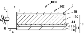
- a photoelectric conversion element 10C shown in FIG. 3 schematically shows another preferred embodiment of the photoelectric conversion element of the present invention.
- the photoelectric conversion element 10C is different from the photoelectric conversion element 10B illustrated in FIG. 2 in that the porous layer 12 is not provided, but is configured in the same manner as the photoelectric conversion element 10B except for this point. That is, in the photoelectric conversion element 10 ⁇ / b> C, the photosensitive layer 13 ⁇ / b> C is formed in a thick film shape on the surface of the blocking layer 14. In the photoelectric conversion element 10 ⁇ / b> C, the hole transport layer 3 ⁇ / b> B can be provided thick like the hole transport layer 3 ⁇ / b> A.
- a photoelectric conversion element 10D shown in FIG. 4 schematically shows another preferred embodiment of the photoelectric conversion element of the present invention.
- This photoelectric conversion element 10D is different from the photoelectric conversion element 10C shown in FIG. 3 in that an electron transport layer 15 is provided instead of the blocking layer 14, but is otherwise configured in the same manner as the photoelectric conversion element 10C.
- the first electrode 1 ⁇ / b> D includes a conductive support 11 and an electron transport layer 15 and a photosensitive layer 13 ⁇ / b> C that are sequentially formed on the conductive support 11.
- This photoelectric conversion element 10D is preferable in that each layer can be formed of an organic material. As a result, the productivity of the photoelectric conversion element is improved, and it is possible to make it thinner or flexible.
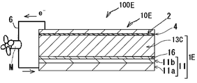
- a photoelectric conversion element 10E shown in FIG. 5 schematically shows still another preferred embodiment of the photoelectric conversion element of the present invention.
- a system 100E including the photoelectric conversion element 10E is a system applied to battery use as in the system 100A.
- the photoelectric conversion element 10 ⁇ / b> E has a first electrode 1 ⁇ / b> E, a second electrode 2, and an electron transport layer 4 between the first electrode 1 ⁇ / b> E and the second electrode 2.
- the first electrode 1 ⁇ / b> E includes a conductive support 11 and a hole transport layer 16 and a photosensitive layer 13 ⁇ / b> C, which are sequentially formed on the conductive support 11.
- This photoelectric conversion element 10E is preferable in that each layer can be formed of an organic material, like the photoelectric conversion element 10D.
- a photoelectric conversion element 10F shown in FIG. 6 schematically shows still another preferred embodiment of the photoelectric conversion element of the present invention.
- the photoelectric conversion element 10F is different from the photoelectric conversion element 10B illustrated in FIG. 2 in that the hole transport layer 3B is not provided, but is configured in the same manner as the photoelectric conversion element 10B except for this point.
- the system 100 to which the photoelectric conversion element 10 is applied functions as a solar cell as follows. That is, in the photoelectric conversion element 10, light that has passed through the conductive support 11 or passed through the second electrode 2 and entered the photosensitive layer 13 excites the light absorber. The excited light absorber has electrons with high energy and can emit these electrons. The light absorber that has released electrons with high energy becomes an oxidant.
- the photoelectric conversion elements 10A to 10D and 10F electrons emitted from the light absorber move between the light absorbers and reach the conductive support 11. After the electrons that have reached the conductive support 11 work in the external circuit 6, they pass through the second electrode 2 (if there is a hole transport layer 3, further via the hole transport layer 3), and then the photosensitive layer Return to 13. The light absorber is reduced by the electrons returning to the photosensitive layer 13.
- the photoelectric conversion element 10E the electrons emitted from the light absorber reach the second electrode 2 from the photosensitive layer 13C through the electron transport layer 4, and after working in the external circuit 6, the conductive support 11 Then, the process returns to the photosensitive layer 13. The light absorber is reduced by the electrons returning to the photosensitive layer 13.
- the system 100 functions as a solar cell by repeating such a cycle of excitation and electron transfer of the light absorber.
- the way in which electrons flow from the photosensitive layer 13 to the conductive support 11 differs depending on the presence and type of the porous layer 12 and the like.
- the porous layer 12 can be formed with an insulator other than the conventional semiconductor.
- the porous layer 12 is formed of a semiconductor, electron conduction in which electrons move inside or between the semiconductor particles of the porous layer 12 also occurs.
- the porous layer 12 is formed of an insulator, electron conduction in the porous layer 12 does not occur.
- a relatively high electromotive force can be obtained by using aluminum oxide (Al 2 O 3 ) particles as the insulator particles.
- Al 2 O 3 aluminum oxide
- the blocking layer 14 as the other layer is formed of a conductor or a semiconductor, electron conduction in the blocking layer 14 occurs. Electron conduction also occurs in the electron transport layer 15.
- the photoelectric conversion element and the solar cell of the present invention are not limited to the above-described preferred embodiments, and the configuration of each embodiment can be appropriately combined between the respective embodiments without departing from the spirit of the present invention.
- the photoelectric conversion element 10C or 10D may have a configuration in which the hole transport layer 3B is not provided as in the photoelectric conversion element 10F.
- the material and each member which are used for a photoelectric conversion element or a solar cell can be prepared by a conventional method except the material and member prescribed
- it can refer also about the material and each member which are used for a dye-sensitized solar cell.
- the dye-sensitized solar cell include Japanese Patent Application Laid-Open No. 2001-291534, US Pat. No. 4,927,721, US Pat. No. 4,684,537, US Pat. No. 5,0843,65.
- the first electrode 1 has a conductive support 11 and a photosensitive layer 13 and functions as a working electrode in the photoelectric conversion element 10. As shown in FIGS. 1 to 6, the first electrode 1 preferably has at least one of a porous layer 12, a blocking layer 14, an electron transport layer 15 and a hole transport layer 16. The first electrode 1 preferably has at least the blocking layer 14 in terms of prevention of short circuit, and more preferably has the porous layer 12 and the blocking layer 14 in terms of light absorption efficiency and prevention of short circuit. Moreover, it is preferable that the 1st electrode 1 has the electron transport layer 15 or the hole transport layer 16 formed with the organic material from the point of the improvement of productivity of a photoelectric conversion element, thickness reduction, or flexibility.
- the conductive support 11 is not particularly limited as long as it has conductivity and can support the photosensitive layer 13 and the like.
- the conductive support 11 includes a conductive material such as a metal, or a glass or plastic support 11a and a transparent electrode 11b as a conductive film formed on the surface of the support 11a. The structure which has is preferable.
- a conductive support 11 in which a transparent metal electrode 11b is formed by coating a conductive metal oxide on the surface of a glass or plastic support 11a is more preferable.
- the support 11a formed of plastic include a transparent polymer film described in paragraph No. 0153 of JP-A-2001-291534.
- ceramic Japanese Patent Laid-Open No. 2005-135902
- conductive resin Japanese Patent Laid-Open No. 2001-160425
- tin oxide As the metal oxide, tin oxide (TO) is preferable, and fluorine-doped tin oxide such as indium-tin oxide (tin-doped indium oxide; ITO) and fluorine-doped tin oxide (FTO) is particularly preferable.
- the coating amount of the metal oxide at this time is preferably 0.1 to 100 g per 1 m 2 of the surface area of the support 11a. When the conductive support 11 is used, light is preferably incident from the support 11a side.
- the conductive support 11 is substantially transparent.
- substantially transparent means that the transmittance of light (wavelength 300 to 1200 nm) is 10% or more, preferably 50% or more, and particularly preferably 80% or more.
- the thicknesses of the support 11a and the conductive support 11 are not particularly limited, and are set to appropriate thicknesses.
- the thickness is preferably 0.01 ⁇ m to 10 mm, more preferably 0.1 ⁇ m to 5 mm, and particularly preferably 0.3 ⁇ m to 4 mm.
- the film thickness of the transparent electrode 11b is not particularly limited, and is preferably 0.01 to 30 ⁇ m, more preferably 0.03 to 25 ⁇ m, and more preferably 0.05 to 20 ⁇ m. It is particularly preferred that
- the conductive support 11 or the support 11a may have a light management function on the surface.
- the surface of the conductive support 11 or the support 11a may have an antireflection film in which high refractive films and low refractive index oxide films are alternately stacked as described in JP-A-2003-123859.
- the light guide function described in JP-A-2002-260746 may be provided.
- a blocking layer 14 is provided.
- a photoelectric conversion element and a solar cell for example, when the photosensitive layer 13 or the hole transport layer 3 and the transparent electrode 11b are electrically connected, a reverse current is generated.
- the blocking layer 14 functions to prevent this reverse current.
- the blocking layer 14 is also referred to as a short circuit prevention layer.
- the blocking layer 14 can also function as a scaffold carrying the light absorber.
- This blocking layer 14 may also be provided when the photoelectric conversion element has an electron transport layer.
- the photoelectric conversion element 10D it may be provided between the conductive support 11 and the electron transport layer 15, and in the case of the photoelectric conversion element 10E, it is provided between the second electrode 2 and the electron transport layer 4. May be.
- the material for forming the blocking layer 14 is not particularly limited as long as it is a material capable of fulfilling the above functions, but is a substance that transmits visible light and is an insulating substance for the conductive support 11 (transparent electrode 11b) and the like. It is preferable that Specifically, the “insulating substance with respect to the conductive support 11 (transparent electrode 11b)” specifically refers to a material whose conduction band energy level forms the conductive support 11 (metal oxide forming the transparent electrode 11b). A compound (n-type semiconductor compound) that is higher than the energy level of the conduction band of the material and lower than the energy level of the conduction band of the material constituting the porous layer 12 and the ground state of the light absorber.
- Examples of the material for forming the blocking layer 14 include silicon oxide, magnesium oxide, aluminum oxide, calcium carbonate, cesium carbonate, polyvinyl alcohol, and polyurethane.
- the material generally used for the photoelectric conversion material may be used, and examples thereof include titanium oxide, tin oxide, zinc oxide, niobium oxide, and tungsten oxide. Of these, titanium oxide, tin oxide, magnesium oxide, aluminum oxide and the like are preferable.
- the thickness of the blocking layer 14 is preferably 0.001 to 10 ⁇ m, more preferably 0.005 to 1 ⁇ m, and particularly preferably 0.01 to 0.1 ⁇ m.
- the film thickness of each layer can be measured by observing the cross section of the photoelectric conversion element 10 using a scanning electron microscope (SEM) or the like.
- the porous layer 12 is preferably provided on the transparent electrode 11b.
- the blocking layer 14 is preferably formed on the blocking layer 14.
- the porous layer 12 is a layer that functions as a scaffold for carrying the photosensitive layer 13 on the surface.
- the porous layer 12 is preferably a fine particle layer having pores, in which fine particles of the material forming the porous layer 12 are deposited or adhered.
- the porous layer 12 may be a fine particle layer in which two or more kinds of fine particles are deposited.
- the amount of light absorbent supported (adsorption amount) can be increased.
- the surface area of the porous layer 12 it is preferable to increase the surface area of the individual fine particles constituting the porous layer 12.
- the surface area of the fine particles is preferably 10 times or more, more than 100 times the projected area. It is more preferable.
- the particle diameter of the fine particles forming the porous layer 12 is preferably 0.001 to 1 ⁇ m as the primary particle in the average particle diameter using the diameter when the projected area is converted into a circle.
- the average particle diameter of the fine particles is preferably 0.01 to 100 ⁇ m as the average particle diameter of the dispersion.
- the material for forming the porous layer 12 is not particularly limited with respect to conductivity, and may be an insulator (insulating material), a conductive material, or a semiconductor (semiconductive material).
- Examples of the material for forming the porous layer 12 include metal chalcogenides (eg, oxides, sulfides, selenides, etc.), compounds having a perovskite crystal structure (excluding perovskite compounds used as a light absorber), silicon. These oxides (for example, silicon dioxide, zeolite) or carbon nanotubes (including carbon nanowires and carbon nanorods) can be used.
- the metal chalcogenide is not particularly limited, but is preferably titanium, tin, zinc, tungsten, zirconium, hafnium, strontium, indium, cerium, yttrium, lanthanum, vanadium, niobium, aluminum or tantalum oxide, cadmium sulfide. , Cadmium selenide and the like.
- Examples of the crystal structure of the metal chalcogenide include an anatase type, brookite type and rutile type, and anatase type and brookite type are preferable.
- the compound having a perovskite crystal structure is not particularly limited, and examples thereof include transition metal oxides.
- transition metal oxides For example, strontium titanate, calcium titanate, barium titanate, lead titanate, barium zirconate, barium stannate, lead zirconate, strontium zirconate, strontium tantalate, potassium niobate, bismuth ferrate, strontium barium titanate , Barium lanthanum titanate, calcium titanate, sodium titanate, bismuth titanate.
- strontium titanate, calcium titanate and the like are preferable.
- the carbon nanotube has a shape obtained by rounding a carbon film (graphene sheet) into a cylindrical shape.
- Carbon nanotubes are single-walled carbon nanotubes (SWCNT) in which one graphene sheet is wound in a cylindrical shape, double-walled carbon nanotubes (DWCNT) in which two graphene sheets are wound in a concentric shape, and multiple graphene sheets are concentric
- SWCNT single-walled carbon nanotubes
- DWCNT double-walled carbon nanotubes
- MWCNT multi-walled carbon nanotubes
- any carbon nanotube is not particularly limited and can be used.
- the material for forming the porous layer 12 is preferably titanium, tin, zinc, zirconium, aluminum or silicon oxide, or carbon nanotube, more preferably titanium oxide or aluminum oxide.
- the porous layer 12 may be formed of at least one of the above-described metal chalcogenide, compound having a perovskite crystal structure, silicon oxide, and carbon nanotube, and may be formed of a plurality of types. .
- the thickness of the porous layer 12 is not particularly limited, but is usually in the range of 0.05 to 100 ⁇ m, preferably in the range of 0.1 to 100 ⁇ m. When used as a solar cell, the thickness is preferably 0.1 to 50 ⁇ m, more preferably 0.2 to 30 ⁇ m, and still more preferably 0.3 to 30 ⁇ m.
- the electron transport layer 15 is preferably provided on the surface of the transparent electrode 11b.
- the electron transport layer 15 has a function of transporting electrons generated in the photosensitive layer 13 to the conductive support 11.
- the electron transport layer 15 is formed of an electron transport material that can exhibit this function.
- the electron transport material is not particularly limited, but an organic material (organic electron transport material) is preferable.
- the organic electron transport material examples include fullerene compounds such as [6,6] -Phenyl-C61-Butylic Acid Methyl Ester (PC 61 BM), perylene compounds such as perylene tetracarboxydiimide (PTCDI), and other tetracyanoquinodimethanes. Examples thereof include a low molecular compound such as (TCNQ) or a high molecular compound.
- the thickness of the electron transport layer 15 is not particularly limited, but is preferably 0.001 to 10 ⁇ m, and more preferably 0.01 to 1 ⁇ m.
- the hole transport layer 16 is preferably provided on the surface of the transparent electrode 11b.
- the hole transport layer 16 is the same as the hole transport layer 3 described later except that the position where it is formed is different.
- the photosensitive layer 13 has a perovskite crystal structure having an organic cation represented by the above formula (IA), a cation of a metal atom, and an anion of an anionic atom or atomic group.
- a porous layer 12 photoelectric conversion elements 10A, 10B and 10F
- a blocking layer 14 photoelectric conversion element 10C
- an electron transport layer 15 photoelectric conversion element 10D
- It is provided on the surface of each layer of the hole transport layer 16 (photoelectric conversion element 10E) (including the inner surface of the recess when the surface on which the photosensitive layer 13 is provided is uneven).
- the light absorber only needs to contain at least one of the specific perovskite compounds, and may contain two or more perovskite compounds.
- the light absorber may contain a light absorber other than the perovskite compound in combination with the perovskite compound.
- Examples of the light absorber other than the perovskite compound include metal complex dyes and organic dyes.
- the ratio of the perovskite compound to other light absorbers is not particularly limited.
- the photosensitive layer 13 may be a single layer or a laminate of two or more layers.
- the photosensitive layer 13 may be a laminated structure in which layers made of different light absorbers are laminated, and an intermediate including a hole transport material between the photosensitive layer and the photosensitive layer.
- a laminated structure having layers may also be used.
- the form that the photosensitive layer 13 can take is as described above.
- the photosensitive layer 13 is preferably provided on the surface of the porous layer 12 or the blocking layer 14 so that electrons excited on the conductive support 11 flow. At this time, the photosensitive layer 13 may be provided on the entire surface, or may be provided on a part of the surface. When the porous layer 12 is used, the photosensitive layer 13 is provided inside the pores of the porous layer 12. May be.
- the film thickness of the photosensitive layer 13 is appropriately set according to the form that the photosensitive layer can take, and is not particularly limited.
- the film thickness of the photosensitive layer 13 is, for example, preferably 0.001 to 100 ⁇ m, more preferably 0.01 to 10 ⁇ m, and particularly preferably 0.01 to 5 ⁇ m.
- the total film thickness with the porous layer 12 is preferably 0.01 ⁇ m or more, more preferably 0.05 ⁇ m or more, further preferably 0.1 ⁇ m or more, and 0.2 ⁇ m or more. Particularly preferred.
- the total film thickness is preferably 100 ⁇ m or less, more preferably 50 ⁇ m or less, further preferably 30 ⁇ m or less, and particularly preferably 3 ⁇ m or less.
- the total film thickness can be in a range where the above values are appropriately combined.
- the total film thickness with the porous layer 12 is preferably 0.1 to 100 ⁇ m, more preferably 0.1 to 50 ⁇ m, and particularly preferably 0.2 to 3 ⁇ m.
- the film thickness of the photosensitive layer 13 is the interface with the porous layer 12 along the direction perpendicular to the surface of the porous layer 12. This is the distance from the interface with the hole transport layer 3 described later.
- the total film thickness of the porous layer 12, the photosensitive layer 13, and the hole transport layer 3 is not particularly limited, but is preferably 0.01 ⁇ m or more, more preferably 0.05 ⁇ m or more, and 0 .1 ⁇ m or more is more preferable, and 0.3 ⁇ m or more is particularly preferable.
- the total film thickness is preferably 200 ⁇ m or less, more preferably 50 ⁇ m or less, further preferably 30 ⁇ m or less, and particularly preferably 5 ⁇ m or less.
- the total film thickness can be in a range where the above values are appropriately combined.
- the thickness of the photosensitive layer is larger than that of the photosensitive layer shown in FIG. 1, but the perovskite type light absorber represented by the formula (I) used in the present invention is different from other perovskite types. Like a compound, it can be a hole transport material.
- the perovskite type light absorber may be used in an amount that covers at least a part of the surface of the porous layer 12 or the blocking layer 14 where light is incident, and is preferably an amount that covers the entire surface.
- the content of the perovskite compound is usually 1 to 100% by mass.
- the photosensitive layer 13 contains at least one perovskite compound having a cationic organic group, a metal atom, and an anionic atom or atomic group as a light absorber.
- the cationic organic group, metal atom, and anionic atom or atomic group of the perovskite compound are respectively an organic cation (sometimes referred to as an organic cation A for convenience) and a metal cation (referred to as a cation M for convenience).
- anion sometimes referred to as anion X for convenience).
- the cationic organic group means an organic group having a property of becoming an organic cation in a perovskite crystal structure
- the anionic atom or atomic group is an atom or atom having a property of becoming an anion in a perovskite crystal structure.
- the perovskite compound used in the present invention is a compound having a perovskite crystal structure having an organic cation represented by the following formula (IA), a cation of a metal atom, and an anion of an anionic atom or atomic group.
- RA represents an alkyl group, a cycloalkyl group, an alkenyl group, an alkynyl group, an aryl group, a heteroaryl group, or a group that can be represented by the following formula (2).
- R B represents NR 1 R 2 or (NR 1 R 2 R 3 ) + , and R 1 , R 2 and R 3 each independently represent a hydrogen atom or a substituent.
- L represents a linking group.
- n2 represents an integer of 1 or more. However, (R B ) n2 -L is a group different from R A. n represents a number satisfying 0 ⁇ n ⁇ 1.00.
- Xa represents NR ⁇ 1c> , an oxygen atom, or a sulfur atom.
- R 1b and R 1c each independently represent a hydrogen atom or a substituent.
- *** represents a bond with the nitrogen atom of formula (IA).
- the reason why the variation in wet heat durability can be reduced is as follows. Although not sure yet, it is estimated as follows. That is, in the perovskite compound, when two different organic ammonium cations, ie, an organic ammonium cation having one amino group and an organic ammonium cation having two or more amino groups, are used, the organic ammonium cation having one amino group is used.
- the perovskite crystal structure is stabilized by the amino group of the ammonium cation having two or more amino groups, and defects in the crystal lattice are less likely to occur.
- the interface state with the layer adjacent to the photosensitive layer 13 becomes uniform, and the deterioration in performance caused by moisture or heat under high temperature and high humidity occurs on the interface or in the crystal. It is considered that the variation was reduced by always relaxing a certain part with a certain effect.
- defective crystal parts are greatly affected by the deterioration of performance due to moisture and heat entering the interior due to being placed under high temperature and high humidity, and the fact that the number of defects is reduced by the present invention itself is considered to be the reason why variation can be reduced. It is done.
- the excellent photoelectric conversion efficiency exhibited by the organic ammonium cation having one amino group is not lowered by the presence of an ammonium cation having two or more amino groups, and the battery performance of the perovskite sensitized solar cell is maintained. .
- the light absorber used in the present invention two kinds of cations represented by the above formula (IA) are used in combination as the organic cation constituting the perovskite crystal structure. That is, one is [R A —NH 2 (H + )] and the other is ⁇ [(R B ) n2 —L—NH 2 ] (H + ) ⁇ .
- the perovskite compound only needs to have the two organic cations as the entire light absorber.
- the perovskite compound may be a perovskite compound having two organic cations, a perovskite compound having [R A —NH 2 (H + )], and ⁇ [(R B ) n2 -L—NH 2 ]. It may be a mixture with a perovskite compound having (H + ) ⁇ .
- the organic cation represented by [R A —NH 2 (H + )] is an ammonium cation formed by combining R A and NH 2 in the above formula (IA).
- An organic ammonium cation (R A —NH 3 + ) composed of a reactive organic group A is preferred.
- the organic ammonium cation can take a resonance structure
- the organic cation includes a cation having a resonance structure in addition to the organic ammonium cation.
- the organic cation is bonded to the group that can be represented by the above formula (2) and NH 2.
- an organic amidinium cation which is one of the resonance structures of the organic ammonium cation is also included.
- Examples of the organic amidinium cation comprising an amidinium cationic organic group include a cation represented by the following formula (A am ).
- a cation represented by the following formula (A am ) may be represented as “R 1b C ( ⁇ NH) —NH 3 ” for convenience.
- the alkyl group as R A in formula (IA) may be an unsubstituted alkyl group having no substituent or a substituted alkyl group having a substituent.
- the unsubstituted alkyl group is also a linear alkyl group and is not particularly limited, but is preferably an alkyl group having 1 to 18 carbon atoms, more preferably an alkyl group having 1 to 6 carbon atoms, and an alkyl group having 1 to 3 carbon atoms. More preferred are groups. Examples of such an alkyl group include methyl, ethyl, n-propyl, n-butyl, n-pentyl, n-hexyl, n-decyl and the like.
- the substituted alkyl group is not particularly limited as long as the above-described unsubstituted alkyl group has a substituent T described later, and may be linear or branched.
- the unsubstituted alkyl group before the substituted alkyl group is substituted with the substituent T may be the above-mentioned unsubstituted alkyl group, preferably an alkyl group having 1 to 4 carbon atoms, more preferably 1 to carbon atoms. 3 alkyl group, and more preferably an alkyl group having 1 or 2 carbon atoms.
- the cycloalkyl group is preferably a cycloalkyl group having 3 to 8 carbon atoms, and examples thereof include cyclopropyl, cyclopentyl, and cyclohexyl.
- the alkenyl group may be linear or branched and is preferably an alkenyl group having 2 to 18 carbon atoms, more preferably an alkenyl group having 2 to 6 carbon atoms.
- alkenyl group having 2 to 18 carbon atoms
- alkenyl group having 2 to 6 carbon atoms For example, ethenyl, allyl, butenyl, hexenyl and the like can be mentioned.
- Examples of the branched alkenyl group include 1-methyl-2-propenyl.
- the alkynyl group is preferably an alkynyl group having 2 to 18 carbon atoms, more preferably an alkynyl group having 2 to 4 carbon atoms, and examples thereof include ethynyl, butynyl and hexynyl.
- the aryl group is preferably an aryl group having 6 to 14 carbon atoms, more preferably an aryl group having 6 to 12 carbon atoms, and examples thereof include phenyl.
- the heteroaryl group includes a group consisting only of an aromatic heterocycle and a group consisting of a condensed heterocycle obtained by condensing an aromatic heterocycle with another ring such as an aromatic ring, an aliphatic ring or a heterocycle.
- a ring-constituting hetero atom constituting the aromatic hetero ring a nitrogen atom, an oxygen atom and a sulfur atom are preferable.
- the number of ring members of the aromatic heterocycle is preferably a 3- to 8-membered ring, and more preferably a 5-membered ring or a 6-membered ring.
- the condensed heterocycle including a 5-membered aromatic heterocycle and a 5-membered aromatic heterocycle include a pyrrole ring, an imidazole ring, a pyrazole ring, an oxazole ring, a thiazole ring, a triazole ring, a furan ring, and a thiophene ring. , Benzimidazole ring, benzoxazole ring, benzothiazole ring, indoline ring, and indazole ring.
- Examples of the condensed heterocycle including a 6-membered aromatic heterocycle and a 6-membered aromatic heterocycle include, for example, pyridine ring, pyrimidine ring, pyrazine ring, triazine ring, quinoline ring, and quinazoline ring. Is mentioned.
- X a represents NR 1c , an oxygen atom or a sulfur atom, and NR 1c is preferable.
- R 1c represents a hydrogen atom or a substituent, and is preferably a hydrogen atom, an alkyl group, a cycloalkyl group, an alkenyl group, an alkynyl group, an aryl group or a heteroaryl group, and more preferably a hydrogen atom.
- R 1b represents a hydrogen atom or a substituent, and preferably a hydrogen atom.
- R 1b examples include an alkyl group, a cycloalkyl group, an alkenyl group, an alkynyl group, an aryl group, a heteroaryl group, and an amino group.
- An alkyl group, a cycloalkyl group, an alkenyl group, an alkynyl group, an aryl group and a heteroaryl group, which can be adopted as R 1b and R 1c have the same meanings as those of the above-mentioned groups of RA , and preferred ones are also the same.
- Examples of the group that can be represented by the formula (2) include a (thio) acyl group, a (thio) carbamoyl group, an imidoyl group, and an amidino group.
- the (thio) acyl group includes an acyl group and a thioacyl group.
- the acyl group is preferably an acyl group having 1 to 7 carbon atoms, and examples thereof include formyl, acetyl, propionyl, hexanoyl and the like.
- the thioacyl group is preferably a thioacyl group having 1 to 7 carbon atoms in total, and examples thereof include thioformyl, thioacetyl, thiopropionyl and the like.
- the (thio) carbamoyl group includes a carbamoyl group and a thiocarbamoyl group.
- the amidino group as a group that can be represented by the formula (2) has a structure in which R 1b of the imidoyl group is an amino group and R 1c is a hydrogen atom.
- each group of RA may have is not particularly limited as long as it is a group other than an amino group and a substituted amino group. That is, R A which may have a substituent is different from “(R B ) n2 -L” of another cation described later.
- the substituted amino group includes, for example, a mono- or di-alkylamino group (including a nitrogen-containing aliphatic heterocycle), a mono- or di-arylamino group, an acylamino group, a sulfonamide group, a carbamoyl group, a sulfamoyl group, and the like. Can be mentioned.
- the following substituent T is mentioned as a substituent which each group of RA may have.
- the substituent T is not particularly limited, and examples thereof include an alkyl group, a cycloalkyl group, an alkenyl group, an alkynyl group, an aryl group, a heteroaryl group, an alkoxy group, an alkylthio group, an acyl group, an alkoxycarbonyl group, an alkylcarbonyloxy group, An aryloxycarbonyl group, an aryloxy group, an arylcarbonyloxy group, a halogen atom, a cyano group, a hydroxy group, a mercapto group or a carboxy group can be mentioned.
- R A is a methyl group
- the substituent T does not include an imino ( ⁇ NH) group.
- the substituent T is more preferably an alkyl group, a halogen atom, a cyano group, an aryl group, or a group obtained by combining these, and a halogen atom is particularly preferable.
- an alkyl group, a cycloalkyl group, an alkenyl group, an alkynyl group and an aryl group have the same meaning as the alkyl group, cycloalkyl group, alkenyl group, alkynyl group and aryl group of the above R A , and preferred ones Is the same.
- the heteroaryl group has the same meaning as the heteroaryl group of R A , but a heteroaryl group that does not contain a nitrogen atom as a ring atom is preferable.
- Each of the alkoxy group and the alkylthio group is preferably an alkyl group in which the alkyl portion is the same as the alkyl group of the above RA .
- the acyl group, alkoxycarbonyl group, and alkylcarbonyloxy group each preferably have the same alkyl moiety as the alkyl group of RA above.
- the aryloxycarbonyl group, aryloxy group, and arylcarbonyloxy group each preferably have the same aryl group or heteroaryl group as the aryl group of R A described above.
- the halogen atom is preferably a fluorine atom, a chlorine atom, a bromine atom or an iodine atom, more preferably a fluorine atom, a chlorine atom or a bromine atom, and particularly preferably a fluorine atom.
- each substituent may be further substituted with a substituent.
- the group is not particularly limited as long as it is a group obtained by combining at least two kinds of the above-described substituents. ), A cyanoalkyl group, and the like.
- each substituent T may be the same as or different from each other. Moreover, when several substituent T adjoins (especially when adjoining), they may mutually connect and a ring may be formed.
- a ring for example, an alicyclic ring, an aromatic ring, or a heterocyclic ring, may form a condensed ring in which these are condensed.
- R A is preferably a substituted alkyl group, an unsubstituted alkyl group, an aryl group, a heteroaryl group, or a group that can be represented by the formula (2) among the above-mentioned groups in that variation in photoelectric conversion efficiency can be reduced.
- a substituted alkyl group, an unsubstituted alkyl group, or a group that can be represented by formula (2) is more preferred, an alkyl group that is substituted with a halogen atom or a group that can be represented by formula (2) is more preferred, and a fluorine atom is substituted.
- Particularly preferred are alkyl groups.
- RA and NH 2 or NH 3 + become one of the organic cations.
- the following r-1 to r-23 are shown as specific examples of R A below, but the present invention is not limited thereto.
- “*” represents a bond with a nitrogen atom
- “Me” represents a methyl group
- “Et” represents an ethyl group.
- R B represents an amino group or a substituted amino group or a cation thereof, and specifically represents NR 1 R 2 or (NR 1 R 2 R 3 ) + .
- R 1 , R 2 and R 3 are each independently a hydrogen atom or a substituent.
- R 1 , R 2 and R 3 are each preferably a hydrogen atom from the viewpoint that the perovskite crystal structure can be stabilized and variation in wet heat durability can be kept small.
- R 1 , R 2 or R 3 is a substituent, the substituent is not particularly limited, and examples thereof include the above-described substituent T, and the preferable one is the same, and an alkyl group is particularly preferable.
- the cation may have a counter anion Y B- .
- the counter anion Y B- is not particularly limited, and various anions can be mentioned. Examples of the anion include halide ions (F ⁇ , I ⁇ , Br ⁇ , Cl ⁇ and the like), OH ⁇ , CF 3 SO 3 ⁇ , CH 3 COO ⁇ , SH ⁇ , SCN ⁇ , ClO 4 ⁇ and the like. Of these, halide ions are preferable, and I ⁇ is more preferable.
- Y B- may be incorporated into the perovskite structure represented by the adjacent formula (I).
- L is a linking group, and preferably has at least one group selected from the group consisting of groups represented by the following formulas L-1 to L-9.
- the linking group L has at least one group selected from the group consisting of groups represented by the formulas L-1 to L-9 means that the linking group L has the following formulas L-1 to L-9 A group formed by combining at least two groups selected from the group consisting of groups represented by the following formulas L-1 to L-9 with a group represented by any one of L-9 Including the case of
- R 4 and R 5 are each independently a hydrogen atom or a substituent, and each is preferably a hydrogen atom.
- substituents include the above-described substituent T, preferably an alkyl group and a halogen atom.
- the alkyl group is synonymous with the alkyl group of RA , and the preferred one is the same, but methyl is particularly preferred.
- D 1 represents a nitrogen atom or CR 10 .
- R 10 represents a hydrogen atom or a substituent, and preferably a hydrogen atom.
- substituents include the above-described substituent T, preferably an alkyl group, an alkenyl group, an alkynyl group, an aryl group, a heteroaryl group, and a halogen atom, and more preferably an alkyl group.
- the alkyl group has the same meaning as the alkyl group for RA , but is preferably an alkyl group having 1 to 30 carbon atoms, and more preferably an alkyl group having 1 to 10 carbon atoms.
- R 6 and R 7 are each independently a hydrogen atom or a substituent. When R 6 and R 7 are substituents, they may be the same or different substituents.
- the substituent for R 6 and R 7 is preferably as defined for the above substituent T, and among them, an alkyl group, a cyano group, and a halogen atom are preferable.
- the above formula L-4 is represented as a trans isomer, but may be a cis isomer.
- D 2 represents an oxygen atom, a sulfur atom or NR 11 .
- R 11 has the same meaning as R 10 , and preferred ones are also the same.
- E represents an oxygen atom, a sulfur atom or NR 12 .
- R 12 has the same meaning as R 10 , and preferred ones are also the same.
- R 8 represents a substituent, and has the same meaning as that of the substituent of R 10 , and preferred examples thereof are also the same.
- m1 represents an integer of 0 or more, preferably an integer of 0 to 2, and more preferably 0.
- m2 represents an integer of 0 or more, preferably an integer of 0 to 3, and more preferably 0 (5-membered ring) or 1 (6-membered ring).
- m3 represents an integer of 2 or more, preferably an integer of 2 to 5, and more preferably 3 or 4.
- the ring G represents an aryl ring composed of a carbon atom group necessary for constituting the ring, or a heteroaryl ring composed of the above carbon atom group and Z 1 .
- Z 1 represents a hetero atom or NR 13 .
- the hetero atom include a nitrogen atom, an oxygen atom, and a sulfur atom, and a nitrogen atom or a sulfur atom is preferable.
- R 13 has the same meaning as R 10 , and preferred ones are also the same.
- R 9 represents a substituent, has the same meaning as R 8 , and preferred ones are also the same.
- m4 represents an integer of 0 or more, preferably an integer of 0 to 3, and more preferably 0.
- n5 represents an integer of 0 or more, preferably an integer of 0 to 3, and more preferably 0 (aryl ring) or 1 (heteroaryl ring).
- m6 represents an integer of 2 or more, preferably an integer of 2 to 5, and more preferably 3 or 4.
- the group represented by the formula L-8 is preferably a group represented by the following formula L-10, and the group represented by the formula L-9 is a group represented by the following formula L-11. Is preferred.
- * represents a connecting position with R B , NH 2 or a group represented by the above formula.
- m7 represents an integer of 0 or more, and is synonymous with m2 in the formula L-8, and preferred examples thereof are also the same.
- m8 represents an integer of 3 or more, preferably an integer of 3 to 5, and more preferably 3 or 4.
- Z 1 has the same meaning as Z 1 of the formula L-9, it is preferable also the same.
- m5 represents an integer of 0 or more, and is synonymous with m5 in Formula L-9, and preferred examples are also the same.
- m9 represents an integer of 3 or more, preferably an integer of 3 to 5, and more preferably 3 or 4.
- Ring G represented by formula L-9 and formula L-11 is not particularly limited, but is an aryl ring such as a benzene ring, pyrrole ring, thiophene ring, furan ring, imidazole ring, pyrazole ring, oxazole ring, Examples include a heteroaryl ring such as a thiazole ring, an oxadiazole ring, a thiadiazole ring, an isoxazole ring, an isothiazole ring, a triazole ring, a pyridine ring, a pyrazine ring, a pyrimidine ring, a pyridazine ring, and a triazine ring.
- a pyridine ring or a triazine ring is preferable, and a thiophene ring is more preferable.
- the linking group L is a group formed by combining at least two groups selected from the group consisting of the groups represented by the formulas L-1 to L-9
- the type of group to be combined is particularly It is not limited, A plurality of the same kind of groups may be combined, or all different groups may be combined. In this case, at least two groups selected from the group consisting of the groups represented by the above formulas L-1 to L-9 may be linked to form a ring structure.
- the number of groups to be combined is not particularly limited, and is preferably 2 to 50, for example, and more preferably 2 to 10.
- the chain length of the combined linking group is preferably from 0 to 10, more preferably from 0 to 5.
- the length of the chain of the linking group is the minimum number of atoms constituting a chain between atoms bonded to two amino groups. In the case of having 3 or more amino groups (when there are 3 or more linking positions *), the chain length of each combination of two amino groups is determined, and the largest of these is determined. For example, the minimum number of atoms between two amino groups of the following compound L-2-2 is 5 and the chain length of the linking group is 5.
- the minimum number of atoms between two amino groups of compound L-8-4 is all 3, and the chain length of the linking group is 3.
- the minimum number of atoms between the two amino groups of compound L-9-4 is 2, 3 and 4, and the chain length of the linking group is 4.
- a group formed by combining at least two groups selected from the group consisting of groups represented by formula L-1 to formula L-9 is represented by any one of formulas Lp-1 to Lp-9 below. It is preferably a group.
- R 4 and R 5 have the same meanings as R 4 and R 5 of the group represented by the formula L-1, respectively, and preferred ones are also the same.
- p represents an integer of 2 or more, preferably an integer of 2 to 5, and more preferably 2.
- L p1 represents a single bond or a group represented by the formula Lp-1, and at least one of the plurality of L p1 Is a group represented by the above formula Lp-1, and a plurality of L p1 may be the same or different.
- D 1 has the same meaning as D 1 of the group represented by the formula L-2, and preferred ones are also the same.
- R 6 and R 7 have the same meanings as R 6 and R 7 in the group represented by the formula L-4, respectively, and preferred examples thereof are also the same.
- D 2 has the same meaning as D 2 of the group represented by the formula L-6, and preferred ones are also the same.
- E has the same meaning as E in the group represented by the formula L-7, and the preferable ones are also the same, and two Es may be the same as or different from each other.
- D 2 has the same meaning as D 2 of the group represented by Formula L-6, and preferred ones are also the same.
- R 8 , m1, m2 and m3 are the same as R 8 , m1, m2 and m3 of the group represented by the formula L-8, respectively, and preferred ones are also the same.
- the group formed by the combination is more preferably a group formed by the following combination.
- a group represented by the above formula Lp-1 comprising a combination of a plurality of, preferably 2 to 5, more preferably two groups represented by the formula L-1 (having this group, [(R B ) As amine compounds represented by n2 -L-NH 2 ], for example, the following compounds L-1-1 to L-1-4),
- a group consisting of a combination of one or more groups represented by formula L-3 and one or more groups represented by formula L-1 preferably one group represented by formula L-3 and 4 Examples of the group represented by the above formula Lp-3 consisting of a group represented
- the linking group L has at least one selected from the group consisting of groups represented by formula L-1, formula L-2, formula L-3, formula L-8 and formula L-9. However, it is preferable in that the variation in wet heat durability can be suppressed small. More preferably, it has at least one selected from the group consisting of groups represented by formula L-1, formula L-2, formula L-3, formula L-10, and formula L-11.
- the linking group L more preferably has at least one group selected from the group consisting of groups represented by formula L-2, formula L-3, formula L-10 and formula L-11. Particularly preferably, a group represented by the formula Lp-1, a group represented by the formula Lp-2, a group represented by the formula Lp-3, a group represented by the formula L-10, a group represented by the formula L-11 Group.
- the linking group L preferably has a symmetric structure.
- the symmetry structure may be any of line symmetry, point symmetry, rotational symmetry, and the like.
- the plurality of L p1 are preferably the same.
- n2 represents an integer of 1 or more, preferably an integer of 1 to 5, and more preferably 2 or 3.
- n2 is within the above range, the stability of the perovskite crystal is improved, and variation in wet heat durability can be suppressed to a low level.
- amine compound represented by [(R B ) n2 -L-NH 2 ] in the formula (IA) are shown below, but the present invention is not limited thereto.
- Compound No. “NL” in “L-nL-mL” represents a number corresponding to Formula L-1 to Formula L-9 or Formula Lp-1 to Formula Lp-9, and “mL” represents the number of the exemplified compound in each formula.
- the linking group L in the following compound is a residue obtained by removing all amino groups (excluding those corresponding to the above D 1 , D 2 and E) from the following compound.
- n represents a number satisfying 0 ⁇ n ⁇ 1.00, preferably a number satisfying 0.05 ⁇ n ⁇ 0.90, more preferably 0.10 ⁇ n ⁇ It is a number that satisfies 0.50, and more preferably a number that satisfies 0.15 ⁇ n ⁇ 0.30.
- the above n is determined by the composition ratio (molar ratio) of the synthetic raw material of the perovskite type light absorber.
- the perovskite compound used in the present invention has a metal atom cation (metal cation) in its crystal structure.
- the metal cation is not particularly limited as long as it is a metal atom cation capable of having a perovskite crystal structure.
- metal atoms include calcium (Ca), strontium (Sr), cadmium (Cd), copper (Cu), nickel (Ni), manganese (Mn), iron (Fe), cobalt (Co), Metal atoms such as palladium (Pd), germanium (Ge), tin (Sn), lead (Pb), ytterbium (Yb), europium (Eu), indium (In), and the like can be given.
- the metal cation is particularly preferably a Pb atom or a Sn atom cation.
- the metal cation may be one type or two or more types. In the case of two or more kinds of metal cations, two kinds of cations of Pb atom and Sn atom are preferable.
- the ratio of the metal cation at this time is not particularly limited.
- the perovskite compound used in the present invention has an anion in its crystal structure.
- the anion is preferably an anionic atom such as a halogen atom, or each anion of an anionic atomic group of NCS ⁇ , NCO ⁇ , CH 3 COO ⁇ or HCOO ⁇ .
- a halogen atom anion is more preferable.
- a fluorine atom, a chlorine atom, a bromine atom, an iodine atom, etc. are mentioned, for example.
- the anion may be an anion of one kind of atom or atomic group, or may be an anion of two or more kinds of atoms or atomic groups.
- an anion of iodine atom is preferable.
- there are two or more anions those represented by the following formula (x) are preferred.
- X A1 and X A2 each independently represent an anion different from each other, preferably an anions having different halogen atoms, one being an anion having an iodine atom, and the other being an anion having a chlorine atom or a bromine atom More preferably, it is an anion.
- m is preferably 0.01 to 2.99, more preferably 0.1 to 1.4, and still more preferably 0.5 to 1.0.
- the perovskite compound having each constituent ion described above may be a compound that can have a perovskite crystal structure including each constituent ion, and is preferably a perovskite compound represented by the following formula (I).
- A represents a cationic organic group.
- M represents a metal atom.
- X represents an anionic atom or atomic group.
- a represents 1 or 2
- the cationic organic group represented by A forms an organic cation represented by the above formula (IA) in the perovskite crystal structure. Therefore, the cationic organic group has the same meaning as R A —NH 2 and [(R B ) n2 -L—NH 2 ] in the above formula (IA) described above for the organic cation, and preferable ones are also the same. is there.
- R A , R B , n2 and L are as described above.
- the metal atom represented by M is a metal atom that forms the metal cation in the perovskite crystal structure. Such a metal atom is synonymous with the metal atom demonstrated by the said metal cation, and a preferable thing is also the same.
- the anionic atom or atomic group represented by X is an anionic atom or atomic group forming the anion in the perovskite crystal structure.
- Such an anionic atom or atomic group is synonymous with the anionic atom or atomic group described in the above anion, and preferred ones are also the same.
- the perovskite compound represented by formula (I) is a perovskite compound represented by the following formula (I-1) when a is 1, and when a is 2, the perovskite compound represented by formula (I-2) It is a perovskite compound represented.
- A represents a cationic organic group and has the same meaning as A in the formula (I), and the preferred ones are also the same.
- M represents a metal atom and is synonymous with M in the above formula (I), and preferred ones are also the same.
- X represents an anionic atom or an atomic group, and is synonymous with X in the formula (I), and preferred ones are also the same.
- the perovskite compound used in the present invention may be either a compound represented by formula (I-1) or a compound represented by formula (I-2), or a mixture thereof. Therefore, in the present invention, at least one perovskite compound only needs to be present as a light absorber, and it is not necessary to clearly distinguish which compound is strictly based on the composition formula, molecular formula, crystal structure, and the like. .
- the method for producing the perovskite light absorber used in the present invention is not particularly limited, and can be synthesized according to a known method using R A —NH 2 and (R B ) n2 —L—NH 2 .
- Known methods include, for example, the methods described in Patent Documents 1 and 2 and Non-Patent Document 1.
- the method described in 6050-6051 is also included.
- perovskite type represented by the formula (I) using MX 2 and R A —NH 3 X, (R B ) n2 -L—NH 3 X and MX 2 Light absorbers can be synthesized.
- X represents an atom or atomic group to be an anion, and has the same meaning as X in the above formula (I).
- R A has the same meaning as R A in the above formula (IA)
- R B is L and n2 have the same meanings as R B, L and n2 in each of the aforementioned formula (IA).
- the molar ratio of MX 2 to R A —NH 3 X and (R B ) n2 —L—NH 3 X is adjusted in accordance with n in formula (IA).
- the hole transport layer 3 is provided between the first electrode 1 and the second electrode 2 as in the photoelectric conversion elements 10A to 10D.
- the hole transport layer 3 is preferably provided between the photosensitive layer 13 of the first electrode 1 and the second electrode 2.
- the hole transport layer 3 has a function of replenishing electrons to the oxidant of the light absorber, and is preferably a solid layer (solid hole transport layer).
- the hole transport material forming the hole transport layer 3 may be a liquid material or a solid material, and is not particularly limited. Examples thereof include inorganic materials such as CuI and CuNCS, and organic hole transport materials described in paragraph numbers 0209 to 0212 of JP-A No. 2001-291534, for example.
- the organic hole transport material is preferably a conductive polymer such as polythiophene, polyaniline, polypyrrole and polysilane, a spiro compound in which two rings share a tetrahedral structure such as C and Si, and triarylamine. And aromatic amine compounds such as triphenylene compounds, nitrogen-containing heterocyclic compounds, and liquid crystalline cyano compounds.
- the hole transporting material is preferably an organic hole transporting material that can be applied by solution and becomes solid.
- 2,2 ′, 7,7′-tetrakis- (N, N-di-p-methoxyphenyl) Amine) -9,9-spirobifluorene also referred to as spiro-OMeTAD
- 4- (diethylamino) benzaldehyde diphenylhydrazone
- PEDOT polyethylenedioxythiophene
- the thickness of the hole transport layer 3 is not particularly limited, but is preferably 50 ⁇ m or less, more preferably 1 nm to 10 ⁇ m, further preferably 5 nm to 5 ⁇ m, and particularly preferably 10 nm to 1 ⁇ m.
- the film thickness of the hole transport layer 3 corresponds to the average distance between the second electrode 2 and the surface of the photosensitive layer 13, and the cross section of the photoelectric conversion element is observed using a scanning electron microscope (SEM) or the like. Can be measured.
- the photoelectric conversion element of this invention has the electron carrying layer 4 between the 1st electrode 1 and the 2nd electrode 2 like the photoelectric conversion element 10E.
- the electron transport layer 4 is preferably in contact (laminated) with the photosensitive layer 3C.
- the electron transport layer 4 is the same as the electron transport layer 15 except that the electron transport destination is the second electrode and the position where the electron transport layer 4 is formed is different.
- the second electrode 2 functions as a positive electrode in the solar cell.
- the 2nd electrode 2 will not be specifically limited if it has electroconductivity, Usually, it can be set as the same structure as the electroconductive support body 11. FIG. If the strength is sufficiently maintained, the support 11a is not necessarily required.
- the structure of the second electrode 2 is preferably a structure having a high current collecting effect. In order for light to reach the photosensitive layer 13, at least one of the conductive support 11 and the second electrode 2 must be substantially transparent. In the solar cell of this invention, it is preferable that the electroconductive support body 11 is transparent and sunlight is entered from the support body 11a side. In this case, it is more preferable that the second electrode 2 has a property of reflecting light.
- the second electrode 2 As a material for forming the second electrode 2, for example, platinum (Pt), gold (Au), nickel (Ni), copper (Cu), silver (Ag), indium (In), ruthenium (Ru), palladium (Pd ), Rhodium (Rh), iridium (Ir), osnium (Os), aluminum (Al), and other metals, the above-described conductive metal oxides, carbon materials, and conductive polymers.
- the carbon material may be a conductive material formed by bonding carbon atoms to each other, and examples thereof include fullerene, carbon nanotube, graphite, and graphene.
- the second electrode 2 is preferably a metal or conductive metal oxide thin film (including a thin film formed by vapor deposition), or a glass substrate or plastic substrate having this thin film.
- a metal or conductive metal oxide thin film including a thin film formed by vapor deposition
- a glass substrate or plastic substrate having this thin film.
- glass substrate or plastic substrate glass having a thin film of gold or platinum or glass on which platinum is deposited is preferable.
- the film thickness of the second electrode 2 is not particularly limited, but is preferably 0.01 to 100 ⁇ m, more preferably 0.01 to 10 ⁇ m, and particularly preferably 0.01 to 1 ⁇ m.
- a spacer or a separator can be used instead of the blocking layer 14 or together with the blocking layer 14.
- a hole blocking layer may be provided between the second electrode 2 and the hole transport layer 3.
- the solar cell of this invention is comprised using the photoelectric conversion element of this invention.
- a photoelectric conversion element 10 configured to cause the external circuit 6 to work can be used as a solar cell.
- the external circuit 6 connected to the first electrode 1 (conductive support 11) and the second electrode 2 known ones can be used without particular limitation.
- the present invention is disclosed in, for example, Patent Documents 1 and 2 and Non-Patent Document 1, J. Pat. Am. Chem. Soc. 2009, 131 (17), p. 6050-6051 and Science, 338, p. 643 (2012).
- the photoelectric conversion element and the solar cell of the present invention include the photosensitive layer 13 formed of the perovskite compound represented by the formula (I), and the amount of decrease in battery performance under a high temperature and high humidity environment. Is small among solar cells and exhibits stable battery performance.
- the photoelectric conversion element and solar cell of the present invention can be produced by known production methods such as Patent Documents 1 and 2 and Non-Patent Document 1, and J. Org. Am. Chem. Soc. 2009, 131 (17), p. 6050-6051, Science, 338, p. 643 (2012) and the like.
- the method for producing a photoelectric conversion element and a solar cell of the present invention contains a perovskite type light absorber represented by the above formula (I) as a layer on which a photosensitive layer is formed. And a step of contacting with the liquid. If the manufacturing method of this invention has this process, another process will not be specifically limited.
- At least one of the blocking layer 14, the porous layer 12, the electron transport layer 15, and the hole transport layer 16 is formed on the conductive support 11 as desired.
- the blocking layer 14 can be formed by, for example, a method of applying a dispersion containing the insulating material or a precursor compound thereof on the surface of the conductive support 11 and baking it, or a spray pyrolysis method.
- the material forming the porous layer 12 is preferably used as fine particles, and more preferably used as a dispersion containing fine particles.
- the method for forming the porous layer 12 is not particularly limited, and examples thereof include a wet method, a dry method, and other methods (for example, a method described in Chemical Review, Vol. 110, page 6595 (2010)). It is done. In these methods, the dispersion (paste) is applied to the surface of the conductive support 11 or the surface of the blocking layer 14, and then fired at a temperature of 100 to 800 ° C. for 10 minutes to 10 hours, for example, in air. preferable. Thereby, microparticles
- the firing temperature other than the last firing is preferably performed at a temperature lower than the last firing temperature (the last firing temperature).
- the firing temperature other than the last can be set within a range of 50 to 300 ° C.
- the final firing temperature can be set to be higher than the firing temperature other than the last within the range of 100 to 600 ° C.
- the firing temperature is preferably 60 to 500 ° C.
- the coating amount of the porous material when forming the porous layer 12 is appropriately set according to the thickness of the porous layer 12 and the number of coatings, and is not particularly limited.
- the coating amount of the porous material per 1 m 2 of the surface area of the conductive support 11 is preferably 0.5 to 500 g, and more preferably 5 to 100 g.
- the electron transport layer 15 or the hole transport layer 16 When the electron transport layer 15 or the hole transport layer 16 is provided, it can be formed in the same manner as the hole transport layer 3 or the electron transport layer 4 described later.
- the method for providing the photosensitive layer 13 includes a wet method and a dry method, and is not particularly limited.
- a wet method is preferable, and for example, a method of contacting with a liquid containing a perovskite light absorber (the following forming liquid) is preferable.
- a forming solution for forming a photosensitive layer is prepared.
- This forming solution contains R A —NH 3 X (where R A and X are as described above) and (R B ) n2 -L—NH 3 X (where R B , L, n2 and X is as described above) and MX 2 (wherein M and X are as described above) are mixed at a predetermined molar ratio and then heated.
- This forming liquid is usually a solution (also referred to as a light absorber solution), but may be a suspension.
- the molar ratio of each component in the forming liquid is set according to n in the above formula (IA).
- the heating conditions are not particularly limited, but the heating temperature is preferably 30 to 200 ° C, more preferably 70 to 150 ° C.
- the heating time is preferably 0.5 to 100 hours, more preferably 1 to 3 hours.
- the solvent or dispersion medium those described later can be used.
- the prepared light absorber solution is a layer on which the photosensitive layer 13 is formed (in the photoelectric conversion element 10, any one of the porous layer 12, the blocking layer 14, the electron transport layer 15 and the hole transport layer 16). The surface of the layer).
- the contact temperature is preferably 5 to 100 ° C.
- the immersion time is preferably 5 seconds to 24 hours, more preferably 20 seconds to 1 hour.
- coating a dipping method is included
- any solution may be applied first, but preferably the MX 2 solution is applied first.
- the molar ratio of R A —NH 3 X and (R B ) n2 -L—NH 3 X to MX 2 , coating conditions and drying conditions are the same as in the above method.
- R A —NH 3 X, (R B ) n2 -L—NH 3 X or MX 2 is vapor-deposited instead of applying the R A solution, the R B solution, and the MX 2 solution. You can also.
- the hole transport layer 3 or the electron transport layer 4 is preferably formed on the photosensitive layer 13 thus formed.
- the hole transport layer 3 can be formed by applying a hole transport material solution containing a hole transport material to the photosensitive layer 13 and drying it.
- the hole transport material solution has a coating solution concentration of 0.1 to 1.0 M in that it has excellent coating properties, and if it has the porous layer 12, it easily penetrates into the pores of the porous layer 12. (Mol / L) is preferred.
- the electron transport layer 4 can be formed by applying an electron transport material solution containing an electron transport material to the photosensitive layer 13 and drying it.
- the second electrode 2 is formed, and the photoelectric conversion element is manufactured.
- the film thickness of each layer can be adjusted by appropriately changing the concentration of each dispersion or solution and the number of coatings. For example, when the thick photosensitive layers 13B and 13C are provided, the forming solution may be applied and dried a plurality of times.
- Each of the above-mentioned dispersions and solutions may contain additives such as a dispersion aid and a surfactant as necessary.
- Examples of the solvent or dispersion medium used in the solar cell manufacturing method include, but are not limited to, the solvents described in JP-A No. 2001-291534.
- an organic solvent is preferable, and an alcohol solvent, an amide solvent, a nitrile solvent, a hydrocarbon solvent, a lactone solvent, a halogen solvent, and a mixed solvent of two or more of these are preferable.
- the mixed solvent a mixed solvent of an alcohol solvent and a solvent selected from an amide solvent, a nitrile solvent, or a hydrocarbon solvent is preferable.
- methanol, ethanol, isopropanol, ⁇ -butyrolactone, chlorobenzene, acetonitrile, N, N′-dimethylformamide (DMF), dimethylacetamide, or a mixed solvent thereof is preferable.
- the application method of the solution or dispersant forming each layer is not particularly limited, and spin coating, extrusion die coating, blade coating, bar coating, screen printing, stencil printing, roll coating, curtain coating, spray coating, dip coating, inkjet
- a known coating method such as a printing method or a dipping method can be used. Of these, spin coating, screen printing and the like are preferable.
- the photoelectric conversion element of the present invention may be subjected to an efficiency stabilization treatment such as annealing, light soaking, and leaving in an oxygen atmosphere as necessary.
- the photoelectric conversion element produced as described above can be used as a solar cell by connecting the external circuit 6 to the first electrode 1 and the second electrode 2.
- Example 1 Manufacture of photoelectric conversion element and solar cell (sample No. 101)
- the photoelectric conversion element 10A and the solar cell shown in FIG. 1 were manufactured by the following procedure. When the film thickness of the photosensitive layer 13 is large, it corresponds to the photoelectric conversion element 10B and the solar cell shown in FIG.
- a conductive support 11 was prepared by forming a fluorine-doped SnO 2 conductive film (transparent electrode 11b, film thickness 300 nm) on a glass support 11a (thickness 2 mm). Using the 0.02M blocking layer solution, a blocking layer 14 (film thickness 50 nm) was formed on the SnO 2 conductive film at 450 ° C. by spray pyrolysis.
- Ethyl cellulose, lauric acid and terpineol were added to an ethanol dispersion of titanium oxide (TiO 2 , anatase, average particle size 20 nm) to prepare a titanium oxide paste.
- TiO 2 titanium oxide
- the prepared titanium oxide paste was applied onto the blocking layer 14 by a screen printing method, and baked in air at 500 ° C. for 3 hours. Then, the fired body of the obtained titanium oxide was immersed in a 40 mM TiCl 4 aqueous solution, heated at 60 ° C. for 1 hour, and subsequently at 500 ° C. for 30 minutes, and the porous layer 12 (thickness 300 nm) made of TiO 2 was obtained. A film was formed.
- N (CH 3 ) 2 CH 2 CH 2 NH 2 (Compound L-1-2) and 57% by mass of hydroiodic acid were added at a molar ratio of 1: 1 to ethanol in the flask and stirred at 0 ° C. for 2 hours. Then, it heated at 50 degreeC and stirred for 1 hour. Then concentrated to give a crude product of N (CH 3) 2 CH 2 CH 2 NH 3 I. The obtained crude product was recrystallized from acetonitrile, and the obtained crystal was collected by filtration and dried under reduced pressure at 50 ° C. for 5 hours to obtain purified N (CH 3 ) 2 CH 2 CH 2 NH 3 I.
- the prepared light absorber solution was applied on the porous layer 12 formed on the conductive support 11 by spin coating (2000 rpm for 60 seconds), and then dried at 100 ° C. for 1 hour using a hot plate.
- the photosensitive layer 13 (thickness 310 nm (including the thickness 300 nm of the porous layer 12)) was provided to produce the first electrode 1.
- the photosensitive layer 13A contained a perovskite compound represented by the formula (I) having an organic cation represented by the formula (IA). Table 1 shows organic cations of formula (IA) and n, and M and X of formula (I) (hereinafter the same).
- Gold was vapor-deposited on the hole transport layer 3A by a vapor deposition method to produce a second electrode 2 (film thickness 100 nm).
- a photoelectric conversion element and a solar cell (sample No. 101) were manufactured.
- Each film thickness was observed and measured by SEM according to the above method.
- each of the obtained photoelectric conversion element and solar cell (sample Nos. 102 to 109, 112, 113, 115 to 138) has an organic cation represented by the formula (IA) in the photosensitive layer 13A. It contained a perovskite compound represented by (I).
- N (CH 3 ) 2 CH 2 CH 2 NH 2 (compound L-1-2) and 57% by mass of hydrobromic acid were added at a molar ratio of 1: 1 to ethanol in the flask, and the mixture was stirred at 0 ° C. for 2 hours. After stirring, the mixture was heated to 50 ° C. and stirred for 1 hour. Then concentrated to give a crude product of N (CH 3) 2 CH 2 CH 2 NH 3 Br. The obtained crude product was recrystallized from acetonitrile, and the obtained crystals were collected by filtration and dried under reduced pressure at 50 ° C. for 5 hours to obtain purified N (CH 3 ) 2 CH 2 CH 2 NH 3 Br.
- the molar ratio of purified CH 3 NH 3 Br and purified N (CH 3 ) 2 CH 2 CH 2 NH 3 Br and PbBr 2 is 0.5: 0.5: 1.0 (sample No. 110) or 0.1. 9: 0.1: 1.0 (Sample No. 111), after stirring and mixing in DMF at 60 ° C. for 12 hours, filtered through a polytetrafluoroethylene (PTFE) syringe filter to absorb 40% by mass of light An agent solution was prepared.
- PTFE polytetrafluoroethylene
- Ethylenediamine (precursor of compound L-1-4) and 57% by mass of hydroiodic acid were added to ethanol in the flask at a molar ratio of 1: 2, stirred at 0 ° C. for 2 hours, and then heated to 50 ° C. Stir for 1 hour. Then concentrated to give a crude product of NH 2 CH 2 CH 2 NH 2 ⁇ 2HI. The obtained crude product was recrystallized from acetonitrile, and the obtained crystal was collected by filtration and dried under reduced pressure at 50 ° C. for 5 hours to obtain purified NH 2 CH 2 CH 2 NH 2 .2HI.
- purified CH 3 NH 3 I, purified NH 2 CH 2 CH 2 NH 2 .2HI, and PbI 2 were stirred and mixed at a molar ratio of 0.9: 0.1: 1 in DMF at 60 ° C. for 12 hours. It filtered with the fluoroethylene (PTFE) syringe filter, and prepared the 40 mass% light absorber solution.
- PTFE fluoroethylene
- PTFE polytetrafluoroethylene
- Sample No. of solar cell The variation in wet heat durability of photoelectric conversion efficiency was evaluated as follows. Sample No. Ten specimens of each solar cell were produced in the same manner. Using each specimen, an initial battery characteristic test was performed by irradiating 1000 W / m 2 of pseudo-sunlight from a xenon lamp through an AM1.5 filter using a solar simulator “WXS-85H” (manufactured by WACOM). ,went. In this test, the current-voltage characteristics were measured using an IV tester to determine the initial photoelectric conversion efficiency ( ⁇ /%).
- Rate of decrease (%): 100- (photoelectric conversion efficiency over time / initial photoelectric conversion efficiency) ⁇ 100
- the decrease rate of each of the 10 samples calculated in this way was defined as “analyte decrease rate (Bn)” (n represents an integer of 1 to 10).
- the average value of the specimen reduction rate (Bn) of 10 specimens was obtained and used as “average reduction rate (A)”.
- the variation in wet heat durability is a pass level of this test when the evaluation is D or more, preferably C or more.
- a +: 0 or more and ⁇ 0.12 or less A: ⁇ 0.12 exceeding ⁇ 0.14 or less B +: ⁇ 0.14 exceeding ⁇ 0.16 or less B: ⁇ 0.16 exceeding ⁇ 0.18 or less C +: ⁇ 0.18 and over ⁇ 0.20 or less C: ⁇ 0.20 over ⁇ 0.22 or less D: ⁇ 0.22 over ⁇ 0.24 or less E: Over ⁇ 0.24 over ⁇ 0.26 F: exceeds ⁇ 0.26
- sample No. The photoelectric conversion efficiency of the solar cell 101 functioned sufficiently as a solar cell.
- the solar of the present invention provided with a photosensitive layer 13 containing a perovskite type light absorber having a perovskite type crystal structure having an organic cation, a metal cation and an anion represented by the formula (IA)
- All of the batteries were evaluated with respect to variation in wet heat durability of C or more, and it was found that the variation was small and stable battery performance was exhibited. It has also been found that when a photosensitive layer is formed using a light absorbent solution containing this perovskite light absorber, a photoelectric conversion element that exhibits stable battery performance even in a high temperature and high humidity environment can be produced.
- the time-dependent photoelectric conversion efficiency ( ⁇ /%) of the solar cell of the present invention was a photoelectric conversion efficiency sufficient for normal operation as a solar cell.
- n in the formula (IA) is in the range of 0.10 to 0.50, more preferably 0.15 to 0.30, the variation in wet heat durability can be further reduced.
- R A in formula (IA) is an alkyl group substituted with a halogen atom, variation in wet heat durability could be sufficiently suppressed.
- the linking group L of the formula (IA) has a group represented by the formula L-2, formula L-3, formula L-10 or formula L-11, the variation in wet heat durability is excellent. I also understood that.
- Example 2 In this example, the photoelectric conversion element 10C shown in FIG. 3 was manufactured and its characteristics were evaluated.
- the photoelectric conversion element and solar cell of Example 1 the same as the photoelectric conversion element and solar cell (Sample Nos. C101 to c104 and 115, 116) of Example 1 except that the porous layer 12 was not provided.
- photoelectric conversion elements and solar cells (Sample Nos. C201 to c204 and 215, 216) were produced.
- the variation in photoelectric conversion efficiency of the manufactured solar cell was evaluated in the same manner as in Example 1, the sample No. Both the solar cells 215 and 216 exhibited a stable battery performance with small variation in wet heat durability.
- Sample No. None of the solar cells c201 to c204 was able to suppress variation in wet heat durability.
- Example 3 In this example, a photoelectric conversion element (see the photoelectric conversion element 10F shown in FIG. 6) and a solar cell that are not provided with a hole transport layer were manufactured and their characteristics were evaluated.
- the photoelectric conversion element and the solar cell of Example 1 (Sample Nos. C101 to c104 and 115, 116), except that the hole transport layer 3A was not provided
- photoelectric conversion elements and solar cells (Sample Nos. C301 to c304 and 315, 316) were manufactured.
- the variation in photoelectric conversion efficiency of the manufactured solar cell was evaluated in the same manner as in Example 1, the sample No. Both the solar cells 315 and 316 exhibited stable battery performance with small variations in wet heat durability.
- Sample No. None of the solar cells c301 to c304 was able to suppress variation in wet heat durability.
- First electrode 11 Conductive support 11a Support 11b Transparent electrode 12 Porous layer 13A to 13C Photosensitive layer 14 Blocking layer 2 Second electrode 3A, 3B, 16 Hole transport layer 4, 15 Electron transport layer 6 External Circuit (Lead) 10A to 10F Photoelectric conversion elements 100A to 100F System M using a solar cell Electric motor
Abstract
Description
例えば、特許文献1には、CH3NH3MX3(MはPbまたはSnを表し、Xはハロゲン原子を表す。)で表されるペロブスカイトを有する感光層と電解液からなる電解質層とを備えた太陽電池が、記載されている。
また、特許文献2には、フォトルミネセンス用のA/M/X金属ハロゲン化物として、メチルアンモニウムカチオン、グアニジウムカチオン等の1価の有機カチオンを含む化合物が記載されている。
さらに、非特許文献1には、ホルムアミジニウムカチオンとメチルアンモニウムカチオンとの混合物をカチオンAとするペロブスカイト:APbI3を用いた光起電装置が記載されている。 On the other hand, in recent years, research results have been reported that solar cells using metal halides as compounds having a perovskite crystal structure (perovskite compounds) can achieve relatively high conversion efficiency, and are attracting attention.
For example,
Furthermore, Non-Patent
このような状況において、ペロブスカイト化合物を用いて成膜した感光層を備えた太陽電池の電池性能を評価、検討したところ、高温高湿度環境下での電池性能の低下量が太陽電池間で大きく変動し(湿熱耐久性がばらつき)、屋外等の高温高湿度環境下での使用を想定した場合に電池性能の安定性が十分ではないことが分かった。
ここで、高温高湿度環境とは、太陽電池の使用環境を想定したものであり、特に限定されるものではないが、例えば、温度40~85℃、相対湿度50~85%の環境をいう。 As described above, solar cells using a perovskite compound have achieved certain results in improving photoelectric conversion efficiency. However, since this solar cell has just been developed, the battery performance has not yet been fully studied and studied.
Under such circumstances, the battery performance of solar cells with a photosensitive layer formed using a perovskite compound was evaluated and studied. However, it was found that the stability of the battery performance was not sufficient when assumed to be used in a high temperature and high humidity environment such as outdoors.
Here, the high-temperature and high-humidity environment is assumed to be the environment in which the solar cell is used, and is not particularly limited.
<1>光吸収剤を含む感光層を導電性支持体上に有する第一電極と、第一電極に対向する第二電極とを有する光電変換素子であって、上記光吸収剤が、下記式(IA)で表される有機カチオンと、金属原子のカチオンと、アニオン性原子もしくは原子団のアニオンとを有するペロブスカイト型結晶構造を持つ化合物を含む光電変換素子。
式(IA):[RA-NH2(H+)]1-n{[(RB)n2-L-NH2](H+)}n
式中、RAはアルキル基、シクロアルキル基、アルケニル基、アルキニル基、アリール基、ヘテロアリール基または下記式(2)で表すことができる基を表す。RBは、NR1R2または(NR1R2R3)+を表し、R1、R2およびR3は各々独立に水素原子または置換基を表す。Lは連結基を表す。n2は1以上の整数を表す。ただし、(RB)n2-LはRAとは異なる基である。nは0<n<1.00を満たす数を表す。 That is, the above problem has been solved by the following means.
<1> A photoelectric conversion element having a first electrode having a photosensitive layer containing a light absorber on a conductive support and a second electrode facing the first electrode, wherein the light absorber is represented by the following formula: A photoelectric conversion element comprising a compound having a perovskite crystal structure having an organic cation represented by (IA), a cation of a metal atom, and an anion of an anionic atom or atomic group.
Formula (IA): [R A -NH 2 (H + )] 1-n {[(R B ) n2 -L-NH 2 ] (H + )} n
In the formula, RA represents an alkyl group, a cycloalkyl group, an alkenyl group, an alkynyl group, an aryl group, a heteroaryl group, or a group that can be represented by the following formula (2). R B represents NR 1 R 2 or (NR 1 R 2 R 3 ) + , and R 1 , R 2 and R 3 each independently represent a hydrogen atom or a substituent. L represents a linking group. n2 represents an integer of 1 or more. However, (R B ) n2 -L is a group different from R A. n represents a number satisfying 0 <n <1.00.

<2>上記ペロブスカイト型結晶構造を持つ化合物が、下記式(I)で表される<1>に記載の光電変換素子。
式(I):AaMmXx
式中、Aはカチオン性有機基を表す。Mは金属原子を表す。Xはアニオン性原子もしくは原子団を表す。aは1または2を表し、mは1を表し、a、mおよびxはa+2m=xを満たす。 In formula, Xa represents NR <1c> , an oxygen atom, or a sulfur atom. R 1b and R 1c each independently represent a hydrogen atom or a substituent. *** represents a bonding position with the N atom in the formula (IA).
<2> The photoelectric conversion element according to <1>, wherein the compound having the perovskite crystal structure is represented by the following formula (I).
Formula (I): A a M m X x
In the formula, A represents a cationic organic group. M represents a metal atom. X represents an anionic atom or atomic group. a represents 1 or 2, m represents 1, and a, m, and x satisfy a + 2m = x.
<4>nが、0.10≦n≦0.50を満たす数を表す<1>~<3>のいずれか1つに記載の光電変換素子。
<5>nが、0.15≦n≦0.30を満たす数を表す<1>~<4>のいずれか1つに記載の光電変換素子。 <3> The photoelectric conversion device according to <1> or <2>, wherein R 1 , R 2, and R 3 are all hydrogen atoms.
<4> The photoelectric conversion element according to any one of <1> to <3>, wherein n represents a number satisfying 0.10 ≦ n ≦ 0.50.
The photoelectric conversion element according to any one of <1> to <4>, wherein <5> n represents a number satisfying 0.15 ≦ n ≦ 0.30.


<9>n2が、2以上の整数である<1>~<8>のいずれか1つに記載の光電変換素子。
<10>金属原子のカチオンが、鉛およびスズからなる群より選択される少なくとも1種の金属カチオンである<1>~<9>のいずれか1つに記載の光電変換素子。
<11>アニオンが、ハロゲン原子のアニオンである<1>~<10>のいずれか1つに記載の光電変換素子。
<12>導電性支持体と感光層との間に多孔質層を有する<1>~<11>のいずれか1つに記載の光電変換素子。
<13>第一電極と第二電極の間に正孔輸送層を有する<1>~<12>のいずれか1つに記載の光電変換素子。
<14>上記<1>~<13>のいずれかに記載の光電変換素子を用いた太陽電池。 <8> The photoelectric conversion device according to any one of <1> to <7>, wherein R A is an alkyl group substituted with a halogen atom.
<9> The photoelectric conversion device according to any one of <1> to <8>, wherein n2 is an integer of 2 or more.
<10> The photoelectric conversion element according to any one of <1> to <9>, wherein the cation of the metal atom is at least one metal cation selected from the group consisting of lead and tin.
<11> The photoelectric conversion device according to any one of <1> to <10>, wherein the anion is an anion of a halogen atom.
<12> The photoelectric conversion element according to any one of <1> to <11>, which has a porous layer between the conductive support and the photosensitive layer.
<13> The photoelectric conversion element according to any one of <1> to <12>, which has a hole transport layer between the first electrode and the second electrode.
<14> A solar cell using the photoelectric conversion element according to any one of <1> to <13>.
式(IA):[RA-NH2(H+)]1-n{[(RB)n2-L-NH2](H+)}n
式中、RAはアルキル基、シクロアルキル基、アルケニル基、アルキニル基、アリール基、ヘテロアリール基または下記式(2)で表すことができる基を表す。RBは、NR1R2または(NR1R2R3)+を表し、R1、R2およびR3は各々独立に水素原子または置換基を表す。Lは連結基を表す。n2は1以上の整数を表す。ただし、(RB)n2-LはRAとは異なる基である。nは0<n<1.00を満たす数を表す。 <15> A layer provided on a conductive support and on which a photosensitive layer is formed includes an organic cation represented by the following formula (IA), a cation of a metal atom, and an anion of an anionic atom or atomic group The manufacturing method of the photoelectric conversion element made to contact the liquid containing the compound which has perovskite type crystal structure which has these.
Formula (IA): [R A -NH 2 (H + )] 1-n {[(R B ) n2 -L-NH 2 ] (H + )} n
In the formula, RA represents an alkyl group, a cycloalkyl group, an alkenyl group, an alkynyl group, an aryl group, a heteroaryl group, or a group that can be represented by the following formula (2). R B represents NR 1 R 2 or (NR 1 R 2 R 3 ) + , and R 1 , R 2 and R 3 each independently represent a hydrogen atom or a substituent. L represents a linking group. n2 represents an integer of 1 or more. However, (R B ) n2 -L is a group different from R A. n represents a number satisfying 0 <n <1.00.

また、上記のような安定した電池性能を発揮する光電変換素子を製造する方法を提供することができる。
本発明の上記および他の特徴および利点は、適宜添付の図面を参照して、下記の記載からより明らかになるであろう。 INDUSTRIAL APPLICABILITY According to the present invention, it is possible to provide a photoelectric conversion element that exhibits a small variation in wet heat durability between products and exhibits stable battery performance, and a solar cell using the photoelectric conversion element.
Moreover, the method of manufacturing the photoelectric conversion element which exhibits the above stable battery performance can be provided.
The above and other features and advantages of the present invention will become more apparent from the following description, with reference where appropriate to the accompanying drawings.
本発明の光電変換素子は、導電性支持体および導電性支持体上に設けられた感光層を有する第一電極と、第一電極に対向する第二電極とを有する。この感光層は、上記式(IA)で表される有機カチオンと、金属原子のカチオンと、アニオン性原子もしくは原子団のアニオンとを有するペロブスカイト型結晶構造を持つ化合物(ペロブスカイト型光吸収剤ともいう)を有してなる。 << Photoelectric conversion element >>
The photoelectric conversion element of the present invention has a first electrode having a conductive support and a photosensitive layer provided on the conductive support, and a second electrode facing the first electrode. This photosensitive layer is a compound having a perovskite crystal structure (also called a perovskite light absorber) having an organic cation represented by the above formula (IA), a cation of a metal atom, and an anion atom or an anion of an atomic group. ).
本発明において、導電性支持体の表面上方に他の層を介して感光層を有する態様としては、例えば、感光層が、多孔質層の表面に薄い膜状等に設けられる態様(図1参照)、多孔質層の表面に厚い膜状に設けられる態様(図2および図6参照)、ブロッキング層の表面に薄い膜状に設けられる態様、および、ブロッキング層の表面に厚い膜状に設けられる態様(図3参照)、電子輸送層の表面に薄い膜状または厚い膜状(図4参照)に設けられる態様、および、正孔輸送層の表面に薄い膜状または厚い膜状(図5参照)に設けられる態様が挙げられる。感光層は、線状または分散状に設けられてもよいが、好ましくは膜状に設けられる。 In the embodiment having the photosensitive layer through another layer above the surface of the conductive support, the other layer provided between the conductive support and the photosensitive layer does not deteriorate the battery performance of the solar cell. If there is no particular limitation. For example, a porous layer, a blocking layer, etc. are mentioned.
In the present invention, for example, the photosensitive layer is provided in the form of a thin film on the surface of the porous layer (see FIG. 1). ), A mode (see FIGS. 2 and 6) provided on the surface of the porous layer (see FIG. 2 and FIG. 6), a mode provided on the surface of the blocking layer as a thin film, and a thick film on the surface of the blocking layer Aspect (see FIG. 3), a mode in which a thin film or a thick film (see FIG. 4) is provided on the surface of the electron transport layer, and a thin or thick film in the surface of the hole transport layer (see FIG. 5) ) Is provided. The photosensitive layer may be provided in a linear or dispersed form, but is preferably provided in a film form.
図1~図6において、同じ符号は同じ構成要素(部材)を意味する。
なお、図1、図2および図6は、多孔質層12を形成する微粒子の大きさを強調して示してある。これらの微粒子は、好ましくは、導電性支持体11に対して水平方向および垂直方向に詰まり(堆積または密着して)、多孔質構造を形成している。 Hereinafter, the preferable aspect of the photoelectric conversion element of this invention is demonstrated.
1 to 6, the same reference numerals mean the same components (members).
1, 2, and 6 emphasize the size of the fine particles forming the
この光電変換素子10Aは、第一電極1Aと、第二電極2と、正孔輸送層3Aとを有している。
第一電極1Aは、支持体11aおよび透明電極11bからなる導電性支持体11と、多孔質層12と、図1において断面領域aを拡大した拡大断面領域aに模式的に示されるように多孔質層12の表面に、ペロブスカイト型光吸収剤で設けられた感光層13Aとを有している。また透明電極11b上にブロッキング層14を有し、ブロッキング層14上に多孔質層12が形成される。このように多孔質層12を有する光電変換素子10Aは、感光層13Aの表面積が大きくなるため、電荷分離および電荷移動効率が向上すると推定される。 As a preferable aspect of the photoelectric conversion element of the present invention, for example, a
The
The first electrode 1A is porous as schematically shown in a
光電変換素子10Eは、第一電極1Eと、第二電極2と、第一電極1Eおよび第二電極2の間に電子輸送層4とを有している。第一電極1Eは、導電性支持体11と、導電性支持体11上に順に形成された、正孔輸送層16および感光層13Cとを有している。この光電変換素子10Eは、光電変換素子10Dと同様に、各層を有機材料で形成できる点で、好ましい。 A
The photoelectric conversion element 10 </ b> E has a
すなわち、光電変換素子10において、導電性支持体11を透過して、または第二電極2を透過して感光層13に入射した光は光吸収剤を励起する。励起された光吸収剤はエネルギーの高い電子を有しており、この電子を放出できる。エネルギーの高い電子を放出した光吸収剤は酸化体となる。 In the present invention, the system 100 to which the photoelectric conversion element 10 is applied functions as a solar cell as follows.
That is, in the photoelectric conversion element 10, light that has passed through the
一方、光電変換素子10Eにおいては、光吸収剤から放出された電子は、感光層13Cから電子輸送層4を経て第二電極2に到達し、外部回路6で仕事をした後に導電性支持体11を経て、感光層13に戻る。感光層13に戻った電子により光吸収剤が還元される。
光電変換素子10においては、このような、上記光吸収剤の励起および電子移動のサイクルを繰り返すことにより、システム100が太陽電池として機能する。 In the
On the other hand, in the
In the photoelectric conversion element 10, the system 100 functions as a solar cell by repeating such a cycle of excitation and electron transfer of the light absorber.
上記他の層としてのブロッキング層14が導体または半導体により形成された場合もブロッキング層14での電子伝導が起こる。
また、電子輸送層15でも電子伝導が起こる。 In the
When the
Electron conduction also occurs in the
以下、この太陽電池を構成する主たる部材とその機能について概略を説明する。 In this invention, the material and each member which are used for a photoelectric conversion element or a solar cell can be prepared by a conventional method except the material and member prescribed | regulated by this invention. For example,
Hereinafter, an outline of main members and functions of the solar cell will be described.
第一電極1は、導電性支持体11と感光層13とを有し、光電変換素子10において作用電極として機能する。
第一電極1は、図1~図6に示されるように、多孔質層12、ブロッキング層14、電子輸送層15および正孔輸送層16の少なくとも1つの層を有することが好ましい。
第一電極1は、短絡防止の点で少なくともブロッキング層14を有することが好ましく、光吸収効率の点および短絡防止の点で多孔質層12およびブロッキング層14を有していることがさらに好ましい。
また、第一電極1は、光電変換素子の生産性の向上、薄型化またはフレキシブル化の点で、有機材料で形成された、電子輸送層15または正孔輸送層16を有することが好ましい。 <
The
As shown in FIGS. 1 to 6, the
The
Moreover, it is preferable that the
導電性支持体11は、導電性を有し、感光層13等を支持できるものであれば特に限定されない。導電性支持体11は、導電性を有する材料、例えば金属で形成された構成、または、ガラスもしくはプラスチックの支持体11aとこの支持体11aの表面に形成された導電膜としての透明電極11bとを有する構成が好ましい。 -Conductive support 11-
The
透明電極11bを設ける場合、透明電極11bの膜厚は、特に限定されず、例えば、0.01~30μmであることが好ましく、0.03~25μmであることがさらに好ましく、0.05~20μmであることが特に好ましい。 The thicknesses of the
When the
本発明においては、光電変換素子10A~10Cおよび10Fのように、好ましくは、透明電極11bの表面に、すなわち、導電性支持体11と、多孔質層12、感光層13または正孔輸送層3等との間に、ブロッキング層14を有している。
光電変換素子および太陽電池において、例えば感光層13または正孔輸送層3と、透明電極11b等とが電気的に接続すると逆電流を生じる。ブロッキング層14は、この逆電流を防止する機能を果たす。ブロッキング層14は短絡防止層ともいう。
ブロッキング層14を、光吸収剤を担持する足場として機能させることもできる。
このブロッキング層14は、光電変換素子が電子輸送層を有する場合にも設けられてもよい。例えば、光電変換素子10Dの場合、導電性支持体11と電子輸送層15との間に設けられてもよく、光電変換素子10Eの場合、第二電極2と電子輸送層4との間に設けられてもよい。 -Blocking layer 14-
In the present invention, like the
In a photoelectric conversion element and a solar cell, for example, when the photosensitive layer 13 or the hole transport layer 3 and the
The
This
ブロッキング層14を形成する材料は、例えば、酸化ケイ素、酸化マグネシウム、酸化アルミニウム、炭酸カルシウム、炭酸セシウム、ポリビニルアルコール、ポリウレタン等が挙げられる。また、一般的に光電変換材料に用いられる材料でもよく、例えば、酸化チタン、酸化スズ、酸化亜鉛、酸化ニオブ、酸化タングステン等も挙げられる。なかでも、酸化チタン、酸化スズ、酸化マグネシウム、酸化アルミニウム等が好ましい。 The material for forming the
Examples of the material for forming the
本発明において、各層の膜厚は、走査型電子顕微鏡(SEM)等を用いて光電変換素子10の断面を観察することにより、測定できる。 The thickness of the
In the present invention, the film thickness of each layer can be measured by observing the cross section of the photoelectric conversion element 10 using a scanning electron microscope (SEM) or the like.
本発明においては、光電変換素子10A、10Bおよび10Fのように、好ましくは、透明電極11b上に多孔質層12を有している。ブロッキング層14を有している場合はブロッキング層14上に形成されることが好ましい。
多孔質層12は、表面に感光層13を担持する足場として機能する層である。太陽電池において、光吸収効率を高めるためには、少なくとも太陽光等の光を受ける部分の表面積を大きくすることが好ましく、多孔質層12の全体としての表面積を大きくすることが好ましい。 -Porous layer 12-
In the present invention, like the
The
多孔質層12の表面積を大きくするには、多孔質層12を構成する個々の微粒子の表面積を大きくすることが好ましい。本発明では、多孔質層12を形成する微粒子を導電性支持体11等に塗設した状態で、この微粒子の表面積が投影面積に対して10倍以上であることが好ましく、100倍以上であることがより好ましい。この上限には特に制限はないが、通常5000倍程度である。多孔質層12を形成する微粒子の粒径は、投影面積を円に換算したときの直径を用いた平均粒径において、1次粒子として0.001~1μmが好ましい。微粒子の分散物を用いて多孔質層12を形成する場合、微粒子の上記平均粒径は、分散物の平均粒径として0.01~100μmが好ましい。 The
In order to increase the surface area of the
多孔質層12を形成する材料としては、例えば、金属のカルコゲニド(例えば酸化物、硫化物、セレン化物等)、ペロブスカイト型結晶構造を有する化合物(光吸収剤として用いるペロブスカイト化合物を除く。)、ケイ素の酸化物(例えば、二酸化ケイ素、ゼオライト)、またはカーボンナノチューブ(カーボンナノワイヤおよびカーボンナノロッド等を含む)を用いることができる。 The material for forming the
Examples of the material for forming the
本発明においては、光電変換素子10Dのように、好ましくは、透明電極11bの表面に電子輸送層15を有している。
電子輸送層15は、感光層13で発生した電子を導電性支持体11へと輸送する機能を有する。電子輸送層15は、この機能を発揮することができる電子輸送材料で形成される。電子輸送材料としては、特に限定されないが、有機材料(有機電子輸送材料)が好ましい。有機電子輸送材料としては、[6,6]-Phenyl-C61-Butyric Acid Methyl Ester(PC61BM)等のフラーレン化合物、ペリレンテトラカルボキシジイミド(PTCDI)等のペリレン化合物、その他、テトラシアノキノジメタン(TCNQ)等の低分子化合物、または、高分子化合物等が挙げられる。
電子輸送層15の膜厚は、特に限定されないが、0.001~10μmが好ましく、0.01~1μmがより好ましい。 -Electron transport layer 15-
In the present invention, like the
The
The thickness of the
本発明においては、光電変換素子10Eのように、好ましくは、透明電極11bの表面に正孔輸送層16を有している。
正孔輸送層16は、形成される位置が異なること以外は、後述する正孔輸送層3と同じである。 -Hole transport layer 16-
In the present invention, like the
The
感光層13は、図1~図6に示されるように、上記式(IA)で表される有機カチオンと、金属原子のカチオンと、アニオン性原子もしくは原子団のアニオンとを有するペロブスカイト型結晶構造を持つ化合物を光吸収剤として、好ましくは、多孔質層12(光電変換素子10A、10Bおよび10F)、ブロッキング層14(光電変換素子10C)、電子輸送層15(光電変換素子10D)、または、正孔輸送層16(光電変換素子10E)の各層の表面(感光層13が設けられる表面が凹凸の場合の凹部内表面を含む。)に、設けられる。
本発明において、光吸収剤は、上記特定のペロブスカイト化合物を少なくとも1種含有していればよく、2種以上のペロブスカイト化合物を含有してもよい。また、光吸収剤は、ペロブスカイト化合物と併せて、ペロブスカイト化合物以外の光吸収剤を含んでいてもよい。ペロブスカイト化合物以外の光吸収剤としては、例えば金属錯体色素および有機色素が挙げられる。このとき、ペロブスカイト化合物と、それ以外の光吸収剤との割合は特に限定されない。 -Photosensitive layer (light absorbing layer) 13-
As shown in FIGS. 1 to 6, the photosensitive layer 13 has a perovskite crystal structure having an organic cation represented by the above formula (IA), a cation of a metal atom, and an anion of an anionic atom or atomic group. As a light absorber, a porous layer 12 (
In the present invention, the light absorber only needs to contain at least one of the specific perovskite compounds, and may contain two or more perovskite compounds. The light absorber may contain a light absorber other than the perovskite compound in combination with the perovskite compound. Examples of the light absorber other than the perovskite compound include metal complex dyes and organic dyes. At this time, the ratio of the perovskite compound to other light absorbers is not particularly limited.
感光層13の膜厚は、感光層がとり得る形態に応じて適宜に設定され、特に限定されない。感光層13の膜厚は、例えば、0.001~100μmが好ましく、0.01~10μmがさらに好ましく、0.01~5μmが特に好ましい。
多孔質層12を有する場合、多孔質層12の膜厚との合計膜厚は、0.01μm以上が好ましく、0.05μm以上がより好ましく、0.1μm以上がさらに好ましく、0.2μm以上が特に好ましい。また、合計膜厚は、100μm以下が好ましく、50μm以下がより好ましく、30μm以下がさらに好ましく、3μm以下が特に好ましい。合計膜厚は、上記値を適宜に組み合わせた範囲とすることができる。例えば、多孔質層12の膜厚との合計膜厚で、0.1~100μmが好ましく、0.1~50μmがさらに好ましく、0.2~3μmが特に好ましい。ここで、図1のように、感光層13が薄い膜状である場合に、感光層13の膜厚は、多孔質層12の表面に垂直な方向に沿う、多孔質層12との界面と後述する正孔輸送層3との界面との距離をいう。 The form that the photosensitive layer 13 can take is as described above. The photosensitive layer 13 is preferably provided on the surface of the
The film thickness of the photosensitive layer 13 is appropriately set according to the form that the photosensitive layer can take, and is not particularly limited. The film thickness of the photosensitive layer 13 is, for example, preferably 0.001 to 100 μm, more preferably 0.01 to 10 μm, and particularly preferably 0.01 to 5 μm.
When the
なお、図2では、図1に示した感光層よりも感光層の厚みが増大したものであるが、本発明で使用する式(I)で表されるペロブスカイト型光吸収剤は、他のペロブスカイト化合物と同様に、正孔輸送材料となりうるものである。 In the photoelectric conversion element 10, the total film thickness of the
In FIG. 2, the thickness of the photosensitive layer is larger than that of the photosensitive layer shown in FIG. 1, but the perovskite type light absorber represented by the formula (I) used in the present invention is different from other perovskite types. Like a compound, it can be a hole transport material.
感光層13中、ペロブスカイト化合物の含有量は、通常1~100質量%である。 The perovskite type light absorber may be used in an amount that covers at least a part of the surface of the
In the photosensitive layer 13, the content of the perovskite compound is usually 1 to 100% by mass.
感光層13は、光吸収剤として、カチオン性有機基と、金属原子と、アニオン性原子または原子団とを有するペロブスカイト化合物を少なくとも1種含有する。
ペロブスカイト化合物のカチオン性有機基、金属原子およびアニオン性原子または原子団は、それぞれ、ペロブスカイト型結晶構造において、有機カチオン(便宜上、有機カチオンAということがある)、金属カチオン(便宜上、カチオンMということがある)およびアニオン(便宜上、アニオンXということがある)の各構成イオンとして存在する。
本発明において、カチオン性有機基とは、ペロブスカイト型結晶構造において有機カチオンになる性質を有する有機基をいい、アニオン性原子または原子団とはペロブスカイト型結晶構造においてアニオンになる性質を有する原子または原子団をいう。
本発明に用いるペロブスカイト化合物は、下記式(IA)で表される有機カチオンと、金属原子のカチオンと、アニオン性原子もしくは原子団のアニオンとを有するペロブスカイト型結晶構造を有する化合物である。 Hereinafter, the light absorber used in the present invention will be described.
The photosensitive layer 13 contains at least one perovskite compound having a cationic organic group, a metal atom, and an anionic atom or atomic group as a light absorber.
In the perovskite crystal structure, the cationic organic group, metal atom, and anionic atom or atomic group of the perovskite compound are respectively an organic cation (sometimes referred to as an organic cation A for convenience) and a metal cation (referred to as a cation M for convenience). And anion (sometimes referred to as anion X for convenience).
In the present invention, the cationic organic group means an organic group having a property of becoming an organic cation in a perovskite crystal structure, and the anionic atom or atomic group is an atom or atom having a property of becoming an anion in a perovskite crystal structure. A group.
The perovskite compound used in the present invention is a compound having a perovskite crystal structure having an organic cation represented by the following formula (IA), a cation of a metal atom, and an anion of an anionic atom or atomic group.
式中、RAはアルキル基、シクロアルキル基、アルケニル基、アルキニル基、アリール基、ヘテロアリール基または下記式(2)で表すことができる基を表す。RBは、NR1R2または(NR1R2R3)+を表し、R1、R2およびR3は各々独立に水素原子または置換基を表す。Lは連結基を表す。n2は1以上の整数を表す。ただし、(RB)n2-LはRAとは異なる基である。nは0<n<1.00を満たす数を表す。 Formula (IA): [R A -NH 2 (H + )] 1-n {[(R B ) n2 -L-NH 2 ] (H + )} n
In the formula, RA represents an alkyl group, a cycloalkyl group, an alkenyl group, an alkynyl group, an aryl group, a heteroaryl group, or a group that can be represented by the following formula (2). R B represents NR 1 R 2 or (NR 1 R 2 R 3 ) + , and R 1 , R 2 and R 3 each independently represent a hydrogen atom or a substituent. L represents a linking group. n2 represents an integer of 1 or more. However, (R B ) n2 -L is a group different from R A. n represents a number satisfying 0 <n <1.00.

また、アミノ基を1つ持つ有機アンモニウムカチオンにより発揮される優れた光電変換効率は、アミノ基を2つ以上持つアンモニウムカチオンの存在によっても低下せず、ペロブスカイト増感太陽電池の電池性能を維持する。 When the perovskite compound that forms the perovskite crystal structure is a perovskite compound that is an organic cation represented by the above formula (IA) as the perovskite compound that forms the photosensitive layer 13, the reason why the variation in wet heat durability can be reduced is as follows. Although not sure yet, it is estimated as follows. That is, in the perovskite compound, when two different organic ammonium cations, ie, an organic ammonium cation having one amino group and an organic ammonium cation having two or more amino groups, are used, the organic ammonium cation having one amino group is used. In the presence of, the perovskite crystal structure is stabilized by the amino group of the ammonium cation having two or more amino groups, and defects in the crystal lattice are less likely to occur. As a result, the interface state with the layer adjacent to the photosensitive layer 13 becomes uniform, and the deterioration in performance caused by moisture or heat under high temperature and high humidity occurs on the interface or in the crystal. It is considered that the variation was reduced by always relaxing a certain part with a certain effect. In addition, defective crystal parts are greatly affected by the deterioration of performance due to moisture and heat entering the interior due to being placed under high temperature and high humidity, and the fact that the number of defects is reduced by the present invention itself is considered to be the reason why variation can be reduced. It is done.
In addition, the excellent photoelectric conversion efficiency exhibited by the organic ammonium cation having one amino group is not lowered by the presence of an ammonium cation having two or more amino groups, and the battery performance of the perovskite sensitized solar cell is maintained. .
本発明においては、ペロブスカイト化合物は、光吸収剤全体として、2つの上記有機カチオンを有していればよい。ペロブスカイト化合物は、2つの有機カチオンを有するペロブスカイト化合物であってもよく、また、[RA-NH2(H+)]を有するペロブスカイト化合物と、{[(RB)n2-L-NH2](H+)}を有するペロブスカイト化合物との混合物であってもよい。 As described above, as the light absorber used in the present invention, two kinds of cations represented by the above formula (IA) are used in combination as the organic cation constituting the perovskite crystal structure. That is, one is [R A —NH 2 (H + )] and the other is {[(R B ) n2 —L—NH 2 ] (H + )}.
In the present invention, the perovskite compound only needs to have the two organic cations as the entire light absorber. The perovskite compound may be a perovskite compound having two organic cations, a perovskite compound having [R A —NH 2 (H + )], and {[(R B ) n2 -L—NH 2 ]. It may be a mixture with a perovskite compound having (H + )}.

無置換アルキル基は、直鎖状のアルキル基でもあり、特に限定されないが、炭素数が1~18のアルキル基が好ましく、1~6のアルキル基がより好ましく、炭素数が1~3のアルキル基がさらに好ましい。このようなアルキル基としては、例えば、メチル、エチル、n-プロピル、n-ブチル、n-ペンチル、n-ヘキシルおよびn-デシル等が挙げられる。
置換アルキル基は、上述の無置換アルキル基が後述する置換基Tを有するものであればよく、直鎖状であっても分岐状であってもよい。置換アルキル基が置換基Tで置換される前の無置換アルキル基は、上述の無置換アルキル基であればよく、好ましくは炭素数1~4のアルキル基であり、より好ましくは炭素数1~3のアルキル基であり、さらに好ましくは炭素数1または2のアルキル基である。
シクロアルキル基は、炭素数が3~8のシクロアルキル基が好ましく、例えば、シクロプロピル、シクロペンチルまたはシクロヘキシル等が挙げられる。 The alkyl group as R A in formula (IA) may be an unsubstituted alkyl group having no substituent or a substituted alkyl group having a substituent.
The unsubstituted alkyl group is also a linear alkyl group and is not particularly limited, but is preferably an alkyl group having 1 to 18 carbon atoms, more preferably an alkyl group having 1 to 6 carbon atoms, and an alkyl group having 1 to 3 carbon atoms. More preferred are groups. Examples of such an alkyl group include methyl, ethyl, n-propyl, n-butyl, n-pentyl, n-hexyl, n-decyl and the like.
The substituted alkyl group is not particularly limited as long as the above-described unsubstituted alkyl group has a substituent T described later, and may be linear or branched. The unsubstituted alkyl group before the substituted alkyl group is substituted with the substituent T may be the above-mentioned unsubstituted alkyl group, preferably an alkyl group having 1 to 4 carbon atoms, more preferably 1 to carbon atoms. 3 alkyl group, and more preferably an alkyl group having 1 or 2 carbon atoms.
The cycloalkyl group is preferably a cycloalkyl group having 3 to 8 carbon atoms, and examples thereof include cyclopropyl, cyclopentyl, and cyclohexyl.
アルキニル基は、炭素数が2~18のアルキニル基が好ましく、炭素数が2~4のアルキニル基がより好ましく、例えば、エチニル、ブチニルまたはヘキシニル等が挙げられる。 The alkenyl group may be linear or branched and is preferably an alkenyl group having 2 to 18 carbon atoms, more preferably an alkenyl group having 2 to 6 carbon atoms. For example, ethenyl, allyl, butenyl, hexenyl and the like can be mentioned. Examples of the branched alkenyl group include 1-methyl-2-propenyl.
The alkynyl group is preferably an alkynyl group having 2 to 18 carbon atoms, more preferably an alkynyl group having 2 to 4 carbon atoms, and examples thereof include ethynyl, butynyl and hexynyl.
ヘテロアリール基は、芳香族ヘテロ環のみからなる基と、芳香族ヘテロ環に他の環、例えば、芳香環、脂肪族環やヘテロ環が縮合した縮合ヘテロ環からなる基とを包含する。
芳香族ヘテロ環を構成する環構成ヘテロ原子としては、窒素原子、酸素原子、硫黄原子が好ましい。また、芳香族ヘテロ環の環員数としては、3~8員環が好ましく、5員環または6員環が好ましい。
5員環の芳香族ヘテロ環および5員環の芳香族ヘテロ環を含む縮合ヘテロ環としては、例えば、ピロール環、イミダゾール環、ピラゾール環、オキサゾール環、チアゾール環、トリアゾール環、フラン環、チオフェン環、ベンゾイミダゾール環、ベンゾオキサゾール環、ベンゾチアゾール環、インドリン環、インダゾール環の各環基が挙げられる。また、6員環の芳香族ヘテロ環および6員環の芳香族ヘテロ環を含む縮合ヘテロ環としては、例えば、ピリジン環、ピリミジン環、ピラジン環、トリアジン環、キノリン環、キナゾリン環の各環基が挙げられる。 The aryl group is preferably an aryl group having 6 to 14 carbon atoms, more preferably an aryl group having 6 to 12 carbon atoms, and examples thereof include phenyl.
The heteroaryl group includes a group consisting only of an aromatic heterocycle and a group consisting of a condensed heterocycle obtained by condensing an aromatic heterocycle with another ring such as an aromatic ring, an aliphatic ring or a heterocycle.
As a ring-constituting hetero atom constituting the aromatic hetero ring, a nitrogen atom, an oxygen atom and a sulfur atom are preferable. Further, the number of ring members of the aromatic heterocycle is preferably a 3- to 8-membered ring, and more preferably a 5-membered ring or a 6-membered ring.
Examples of the condensed heterocycle including a 5-membered aromatic heterocycle and a 5-membered aromatic heterocycle include a pyrrole ring, an imidazole ring, a pyrazole ring, an oxazole ring, a thiazole ring, a triazole ring, a furan ring, and a thiophene ring. , Benzimidazole ring, benzoxazole ring, benzothiazole ring, indoline ring, and indazole ring. Examples of the condensed heterocycle including a 6-membered aromatic heterocycle and a 6-membered aromatic heterocycle include, for example, pyridine ring, pyrimidine ring, pyrazine ring, triazine ring, quinoline ring, and quinazoline ring. Is mentioned.
R1bは、水素原子または置換基を表し、水素原子が好ましい。R1bとして採り得る置換基は、アルキル基、シクロアルキル基、アルケニル基、アルキニル基、アリール基、ヘテロアリール基またはアミノ基が挙げられる。
R1bおよびR1cとしてそれぞれ採り得る、アルキル基、シクロアルキル基、アルケニル基、アルキニル基、アリール基およびヘテロアリール基は、上記RAの各基と同義であり、好ましいものも同じである。 In the group that can be represented by the formula (2), X a represents NR 1c , an oxygen atom or a sulfur atom, and NR 1c is preferable. Here, R 1c represents a hydrogen atom or a substituent, and is preferably a hydrogen atom, an alkyl group, a cycloalkyl group, an alkenyl group, an alkynyl group, an aryl group or a heteroaryl group, and more preferably a hydrogen atom.
R 1b represents a hydrogen atom or a substituent, and preferably a hydrogen atom. Examples of the substituent that can be adopted as R 1b include an alkyl group, a cycloalkyl group, an alkenyl group, an alkynyl group, an aryl group, a heteroaryl group, and an amino group.
An alkyl group, a cycloalkyl group, an alkenyl group, an alkynyl group, an aryl group and a heteroaryl group, which can be adopted as R 1b and R 1c , have the same meanings as those of the above-mentioned groups of RA , and preferred ones are also the same.
(チオ)アシル基は、アシル基およびチオアシル基を包含する。アシル基は、総炭素数が1~7のアシル基が好ましく、例えば、ホルミル、アセチル、プロピオニル、ヘキサノイル等が挙げられる。チオアシル基は、総炭素数が1~7のチオアシル基が好ましく、例えば、チオホルミル、チオアセチル、チオプロピオニル等が挙げられる。
(チオ)カルバモイル基は、カルバモイル基およびチオカルバモイル基を包含する。 Examples of the group that can be represented by the formula (2) include a (thio) acyl group, a (thio) carbamoyl group, an imidoyl group, and an amidino group.
The (thio) acyl group includes an acyl group and a thioacyl group. The acyl group is preferably an acyl group having 1 to 7 carbon atoms, and examples thereof include formyl, acetyl, propionyl, hexanoyl and the like. The thioacyl group is preferably a thioacyl group having 1 to 7 carbon atoms in total, and examples thereof include thioformyl, thioacetyl, thiopropionyl and the like.
The (thio) carbamoyl group includes a carbamoyl group and a thiocarbamoyl group.
式(2)で表すことができる基としてのアミジノ基は、上記イミドイル基のR1bがアミノ基でR1cが水素原子である構造を有する。 The imidoyl group is a group represented by R 1b —C (═NR 1c ) —, wherein R 1b and R 1c are each preferably a hydrogen atom or an alkyl group, and the alkyl group has the same meaning as the alkyl group of R A above. Is more preferable. For example, formimidoyl (HC (= NH)-), acetimidoyl (CH 3 C (= NH)-), propionimidoyl (CH 3 CH 2 C (= NH)-) and the like can be mentioned. Of these, formimidoyl is preferable.
The amidino group as a group that can be represented by the formula (2) has a structure in which R 1b of the imidoyl group is an amino group and R 1c is a hydrogen atom.
置換基Tは、アルキル基、ハロゲン原子、シアノ基、アリール基およびこれらを組み合わせた基がより好ましく、ハロゲン原子が特に好ましい。 The following substituent T is mentioned as a substituent which each group of RA may have. The substituent T is not particularly limited, and examples thereof include an alkyl group, a cycloalkyl group, an alkenyl group, an alkynyl group, an aryl group, a heteroaryl group, an alkoxy group, an alkylthio group, an acyl group, an alkoxycarbonyl group, an alkylcarbonyloxy group, An aryloxycarbonyl group, an aryloxy group, an arylcarbonyloxy group, a halogen atom, a cyano group, a hydroxy group, a mercapto group or a carboxy group can be mentioned. When R A is a methyl group, the substituent T does not include an imino (═NH) group.
The substituent T is more preferably an alkyl group, a halogen atom, a cyano group, an aryl group, or a group obtained by combining these, and a halogen atom is particularly preferable.
アシル基、アルコキシカルボニル基およびアルキルカルボニルオキシ基は、それぞれ、アルキル部分が上記RAのアルキル基と同じアルキル部分を有するのが好ましい。
アリールオキシカルボニル基、アリールオキシ基およびアリールカルボニルオキシ基は、それぞれ、上記RAのアリール基と同じアリール基またはヘテロアリール基を有するものが好ましい。
ハロゲン原子は、フッ素原子、塩素原子、臭素原子およびヨウ素原子が好ましく、フッ素原子、塩素原子および臭素原子がより好ましく、フッ素原子が特に好ましい。 Each of the alkoxy group and the alkylthio group is preferably an alkyl group in which the alkyl portion is the same as the alkyl group of the above RA .
The acyl group, alkoxycarbonyl group, and alkylcarbonyloxy group each preferably have the same alkyl moiety as the alkyl group of RA above.
The aryloxycarbonyl group, aryloxy group, and arylcarbonyloxy group each preferably have the same aryl group or heteroaryl group as the aryl group of R A described above.
The halogen atom is preferably a fluorine atom, a chlorine atom, a bromine atom or an iodine atom, more preferably a fluorine atom, a chlorine atom or a bromine atom, and particularly preferably a fluorine atom.
下記に、RAの具体例として下記r-1~r-23を示すが、これらによって本発明が限定されるものではない。なお、下記具体例において、「*」は窒素原子との結合部を示し、「Me」はメチル基を示し、「Et」はエチル基を示す。 The RA and NH 2 or NH 3 + become one of the organic cations.
The following r-1 to r-23 are shown as specific examples of R A below, but the present invention is not limited thereto. In the following specific examples, “*” represents a bond with a nitrogen atom, “Me” represents a methyl group, and “Et” represents an ethyl group.

RBは、アミノ基もしくは置換アミノ基またはそのカチオンを表し、具体的には、NR1R2または(NR1R2R3)+を表す。ここで、R1、R2およびR3は各々独立に水素原子または置換基である。R1、R2およびR3は、ペロブスカイト結晶構造を安定化させて湿熱耐久性のばらつきを小さく抑えることができる点で、いずれも水素原子であることが好ましい。R1、R2またはR3が置換基である場合、置換基としては、特に限定されず、上記置換基Tが挙げられ、好ましいものも同じであり、特にアルキル基が好ましい。 Another organic cation constituting the perovskite crystal is {[(R B ) n2 -L-NH 2 ] (H + )}.
R B represents an amino group or a substituted amino group or a cation thereof, and specifically represents NR 1 R 2 or (NR 1 R 2 R 3 ) + . Here, R 1 , R 2 and R 3 are each independently a hydrogen atom or a substituent. R 1 , R 2 and R 3 are each preferably a hydrogen atom from the viewpoint that the perovskite crystal structure can be stabilized and variation in wet heat durability can be kept small. When R 1 , R 2 or R 3 is a substituent, the substituent is not particularly limited, and examples thereof include the above-described substituent T, and the preferable one is the same, and an alkyl group is particularly preferable.

式L-1で表される基において、R4およびR5は各々独立に水素原子または置換基であり、いずれも水素原子が好ましい。置換基である場合、置換基としては上記置換基Tが挙げられ、好ましくは、アルキル基、ハロゲン原子である。アルキル基は、RAのアルキル基と同義であり、好ましいものも同じであるが、特に好ましくはメチルである。 In each formula, * represents a connecting position with R B , NH 2 or a group represented by the above formula.
In the group represented by the formula L-1, R 4 and R 5 are each independently a hydrogen atom or a substituent, and each is preferably a hydrogen atom. In the case of a substituent, examples of the substituent include the above-described substituent T, preferably an alkyl group and a halogen atom. The alkyl group is synonymous with the alkyl group of RA , and the preferred one is the same, but methyl is particularly preferred.
なお、上記式L-4はトランス体として表されているが、シス体であってもよい。 In the group represented by the formula L-4, R 6 and R 7 are each independently a hydrogen atom or a substituent. When R 6 and R 7 are substituents, they may be the same or different substituents. The substituent for R 6 and R 7 is preferably as defined for the above substituent T, and among them, an alkyl group, a cyano group, and a halogen atom are preferable.
The above formula L-4 is represented as a trans isomer, but may be a cis isomer.
式L-7で表される基において、Eは酸素原子、硫黄原子またはNR12を表す。R12はR10と同義であり、好ましいものも同じである。 In the group represented by the formula L-6, D 2 represents an oxygen atom, a sulfur atom or NR 11 . R 11 has the same meaning as R 10 , and preferred ones are also the same.
In the group represented by the formula L-7, E represents an oxygen atom, a sulfur atom or NR 12 . R 12 has the same meaning as R 10 , and preferred ones are also the same.
m1は0以上の整数を表し、0~2の整数が好ましく、0であることがより好ましい。
m2は0以上の整数を表し、0~3の整数が好ましく、0(5員環)または1(6員環)であることがより好ましい。
m3は2以上の整数を表し、2~5の整数が好ましく、3または4がより好ましい。 In the group represented by the formula L-8, R 8 represents a substituent, and has the same meaning as that of the substituent of R 10 , and preferred examples thereof are also the same.
m1 represents an integer of 0 or more, preferably an integer of 0 to 2, and more preferably 0.
m2 represents an integer of 0 or more, preferably an integer of 0 to 3, and more preferably 0 (5-membered ring) or 1 (6-membered ring).
m3 represents an integer of 2 or more, preferably an integer of 2 to 5, and more preferably 3 or 4.
Z1はヘテロ原子またはNR13を表す。ヘテロ原子としては、窒素原子、酸素原子または硫黄原子が挙げられ、窒素原子または硫黄原子が好ましい。R13はR10と同義であり、好ましいものも同じである。
R9は置換基を表し、R8と同義であり、好ましいものも同じである。
m4は0以上の整数を表し、0~3の整数が好ましく、0であることがより好ましい。
m5は0以上の整数を表し、0~3の整数が好ましく、0(アリール環)または1(ヘテロアリール環)であることがより好ましい。
m6は2以上の整数を表し、2~5の整数が好ましく、3または4がより好ましい。 In the group represented by the formula L-9, the ring G represents an aryl ring composed of a carbon atom group necessary for constituting the ring, or a heteroaryl ring composed of the above carbon atom group and Z 1 .
Z 1 represents a hetero atom or NR 13 . Examples of the hetero atom include a nitrogen atom, an oxygen atom, and a sulfur atom, and a nitrogen atom or a sulfur atom is preferable. R 13 has the same meaning as R 10 , and preferred ones are also the same.
R 9 represents a substituent, has the same meaning as R 8 , and preferred ones are also the same.
m4 represents an integer of 0 or more, preferably an integer of 0 to 3, and more preferably 0.
m5 represents an integer of 0 or more, preferably an integer of 0 to 3, and more preferably 0 (aryl ring) or 1 (heteroaryl ring).
m6 represents an integer of 2 or more, preferably an integer of 2 to 5, and more preferably 3 or 4.

式L-10で表される基において、m7は0以上の整数を表し、式L-8のm2と同義であり、好ましいものも同じである。m8は3以上の整数を表し、3~5の整数が好ましく、3または4がより好ましい。 In Formula L-10 and Formula L-11, * represents a connecting position with R B , NH 2 or a group represented by the above formula.
In the group represented by the formula L-10, m7 represents an integer of 0 or more, and is synonymous with m2 in the formula L-8, and preferred examples thereof are also the same. m8 represents an integer of 3 or more, preferably an integer of 3 to 5, and more preferably 3 or 4.
このとき、組み合わせてなる連結基の鎖の長さが0~10であるのが好ましく、0~5であるのがより好ましい。ここで、連結基の鎖の長さは、2つのアミノ基に結合する原子間の鎖を構成する最小原子数とする。アミノ基を3個以上有する場合(連結位置*が3以上ある場合)は2つのアミノ基の組み合わせそれぞれの鎖の長さを求め、これらのうち最も大きなものとする。例えば、下記化合物L-2-2の2つのアミノ基間の最小原子数はすべて5であり、連結基の鎖の長さは5である。また、化合物L-8-4の2つのアミノ基間の最小原子数はすべて3であり、連結基の鎖の長さは3である。一方、化合物L-9-4の2つのアミノ基間の最小原子数は2、3および4であり、連結基の鎖の長さは4となる。 The number of groups to be combined is not particularly limited, and is preferably 2 to 50, for example, and more preferably 2 to 10.
At this time, the chain length of the combined linking group is preferably from 0 to 10, more preferably from 0 to 5. Here, the length of the chain of the linking group is the minimum number of atoms constituting a chain between atoms bonded to two amino groups. In the case of having 3 or more amino groups (when there are 3 or more linking positions *), the chain length of each combination of two amino groups is determined, and the largest of these is determined. For example, the minimum number of atoms between two amino groups of the following compound L-2-2 is 5 and the chain length of the linking group is 5. In addition, the minimum number of atoms between two amino groups of compound L-8-4 is all 3, and the chain length of the linking group is 3. On the other hand, the minimum number of atoms between the two amino groups of compound L-9-4 is 2, 3 and 4, and the chain length of the linking group is 4.

式Lp-2~Lp-9のいずれか1つの式で表される各基において、Lp1は単結合または上記式Lp-1で表される基を表し、複数のLp1のうち少なくとも1つは上記式Lp-1で表される基であり、複数のLp1は同一でも異なっていてよい。
式Lp-2で表される基において、D1は、式L-2で表される基のD1と同義であり、好ましいものも同じである。式Lp-4で表される基において、R6およびR7はそれぞれ式L-4で表される基のR6およびR7と同義であり、好ましいものも同じである。式Lp-6で表される基において、D2は式L-6で表される基のD2と同義であり、好ましいものも同じである。式Lp-7で表される基において、Eは式L-7で表される基のEと同義であり、好ましいものも同じであり、2つのEは互いに同一でも異なってもよい。また、D2は式L-6で表される基のD2と同義であり、好ましいものも同じである。式Lp-8で表される基において、R8、m1、m2およびm3はそれぞれ式L-8で表される基のR8、m1、m2およびm3と同義であり、好ましいものも同じである。式Lp-9で表される基において、環G、R9、Z1、m4、m5およびm6はそれぞれ式L-9で表される基の環G、R9、Z1、m4、m5およびm6と同義であり、好ましいものも同じである。 In the group represented by the formula Lp-1, R 4 and R 5 have the same meanings as R 4 and R 5 of the group represented by the formula L-1, respectively, and preferred ones are also the same. p represents an integer of 2 or more, preferably an integer of 2 to 5, and more preferably 2.
In each group represented by any one of the formulas Lp-2 to Lp-9, L p1 represents a single bond or a group represented by the formula Lp-1, and at least one of the plurality of L p1 Is a group represented by the above formula Lp-1, and a plurality of L p1 may be the same or different.
In the group represented by the formula Lp-2, D 1 has the same meaning as D 1 of the group represented by the formula L-2, and preferred ones are also the same. In the group represented by the formula Lp-4, R 6 and R 7 have the same meanings as R 6 and R 7 in the group represented by the formula L-4, respectively, and preferred examples thereof are also the same. In the group represented by the formula Lp-6, D 2 has the same meaning as D 2 of the group represented by the formula L-6, and preferred ones are also the same. In the group represented by the formula Lp-7, E has the same meaning as E in the group represented by the formula L-7, and the preferable ones are also the same, and two Es may be the same as or different from each other. D 2 has the same meaning as D 2 of the group represented by Formula L-6, and preferred ones are also the same. In the group represented by the formula Lp-8, R 8 , m1, m2 and m3 are the same as R 8 , m1, m2 and m3 of the group represented by the formula L-8, respectively, and preferred ones are also the same. . In the group represented by the formula Lp-9, ring G, R 9, Z 1, m4, m5 and m6 ring G of the group represented by each of
複数個の、好ましくは2~5個、より好ましくは2個の式L-1で表される基同士の組み合わせからなる上記式Lp-1で表される基(この基を有する、[(RB)n2-L-NH2]で示されるアミン化合物として、例えば、下記化合物L-1-1~L-1-4)、
1個以上の式L-2で表される基と1個以上の式L-1で表される基の組み合わせからなる基(好ましくは、1個の式L-2で表される基と3個の式Lp-1で表される基からなる上記式Lp-2で表される基、この基を有するアミン化合物として、例えば、下記化合物L-2-1および化合物L-2-2)、
1個以上の式L-3で表される基と1個以上の式L-1で表される基の組み合わせからなる基(好ましくは、1個の式L-3で表される基と4個の式Lp-1で表される基からなる上記式Lp-3で表される基、この基を有するアミン化合物として、例えば、下記化合物L-3-1)、
1個以上の式L-5で表される基と1個以上の式L-1で表される基の組み合わせからなる基(好ましくは、1個の式L-5で表される基と2個の式Lp-1で表される基からなる上記式Lp-5で表される基、この基を有するアミン化合物として、例えば、下記化合物L-5-1)、
1個以上の式L-6で表される基と1個以上の式L-1で表される基の組み合わせからなる基(好ましくは、1個の式L-6で表される基と2個の式Lp-1で表される基からなる上記式Lp-6で表される基、この基を有するアミン化合物として、例えば、下記化合物L-6-1~化合物L-6-3)、
1個以上の式L―6で表される基と1個以上の式L-7で表される基の組み合わせからなる基(好ましくは、1個の式L-6で表される基と2個の式L-7で表される基からなる上記式Lp-7で表される基、この基を有するアミン化合物として、例えば、下記化合物L-7-3)、
1個以上の式L-9で表される基と1個以上の式L-1で表される基の組み合わせからなる基(例えば、1個の式L-9で表される基と2個の式L-1で表される基からなる上記式Lp-9で表される基、この基を有するアミン化合物として、例えば、下記化合物L-9-2)等が挙げられる。 The group formed by the combination is more preferably a group formed by the following combination.
A group represented by the above formula Lp-1 comprising a combination of a plurality of, preferably 2 to 5, more preferably two groups represented by the formula L-1 (having this group, [(R B ) As amine compounds represented by n2 -L-NH 2 ], for example, the following compounds L-1-1 to L-1-4),
A group consisting of a combination of one or more groups represented by Formula L-2 and one or more groups represented by Formula L-1 (preferably one group represented by Formula L-2 and 3 Examples of the group represented by the above formula Lp-2 consisting of a group represented by the formula Lp-1, and amine compounds having this group include, for example, the following compound L-2-1 and compound L-2-2),
A group consisting of a combination of one or more groups represented by formula L-3 and one or more groups represented by formula L-1 (preferably one group represented by formula L-3 and 4 Examples of the group represented by the above formula Lp-3 consisting of a group represented by the formula Lp-1 and an amine compound having this group include, for example, the following compound L-3-1),
A group consisting of a combination of one or more groups represented by formula L-5 and one or more groups represented by formula L-1 (preferably one group represented by formula L-5 and 2 Examples of the group represented by the above formula Lp-5 consisting of a group represented by the formula Lp-1 and an amine compound having this group include, for example, the following compound L-5-1),
A group consisting of a combination of one or more groups represented by formula L-6 and one or more groups represented by formula L-1 (preferably one group represented by formula L-6 and 2 Examples of the group represented by the above formula Lp-6 consisting of a group represented by the formula Lp-1 and amine compounds having this group include the following compounds L-6-1 to L-6-3),
A group consisting of a combination of one or more groups represented by formula L-6 and one or more groups represented by formula L-7 (preferably one group represented by formula L-6 and 2 Examples of the group represented by the above formula Lp-7 consisting of a group represented by the formula L-7, and an amine compound having this group include, for example, the following compound L-7-3),
A group comprising a combination of one or more groups represented by formula L-9 and one or more groups represented by formula L-1 (for example, one group represented by formula L-9 and two groups Examples of the group represented by the above formula Lp-9 consisting of the group represented by formula L-1 and the amine compound having this group include the following compound L-9-2).
なお、下記具体例において、化合物No.「L-nL-mL」の「nL」は上記式L-1~式L-9または式Lp-1~式Lp-9に対応する数字を示し、「mL」は各式における例示化合物の番号を示す。
下記化合物中の連結基Lは下記化合物からすべてのアミノ基(上記D1、D2およびEに相当するものを除く)を除去した残基である。 Specific examples of the amine compound represented by [(R B ) n2 -L-NH 2 ] in the formula (IA) are shown below, but the present invention is not limited thereto.
In the following specific examples, Compound No. “NL” in “L-nL-mL” represents a number corresponding to Formula L-1 to Formula L-9 or Formula Lp-1 to Formula Lp-9, and “mL” represents the number of the exemplified compound in each formula. Indicates.
The linking group L in the following compound is a residue obtained by removing all amino groups (excluding those corresponding to the above D 1 , D 2 and E) from the following compound.

式(x)において、mは0.01~2.99が好ましく、0.1~1.4がより好ましく、0.5~1.0がさらに好ましい。 In the formula (x), X A1 and X A2 each independently represent an anion different from each other, preferably an anions having different halogen atoms, one being an anion having an iodine atom, and the other being an anion having a chlorine atom or a bromine atom More preferably, it is an anion.
In the formula (x), m is preferably 0.01 to 2.99, more preferably 0.1 to 1.4, and still more preferably 0.5 to 1.0.
式(I):AaMmXx
式中、Aはカチオン性有機基を表す。Mは金属原子を表す。Xはアニオン性原子または原子団を表す。
aは1または2を表し、mは1を表し、a、mおよびxはa+2m=xを満たす。 The perovskite compound having each constituent ion described above may be a compound that can have a perovskite crystal structure including each constituent ion, and is preferably a perovskite compound represented by the following formula (I).
Formula (I): A a M m X x
In the formula, A represents a cationic organic group. M represents a metal atom. X represents an anionic atom or atomic group.
a represents 1 or 2, m represents 1, and a, m, and x satisfy a + 2m = x.
式(I-1):AMX3
式(I-2):A2MX4
式(I-1)および式(I-2)において、Aはカチオン性有機基を表し、上記式(I)のAと同義であり、好ましいものも同じである。Mは、金属原子を表し、上記式(I)のMと同義であり、好ましいものも同じである。Xは、アニオン性原子または原子団を表し、上記式(I)のXと同義であり、好ましいものも同じである。 The perovskite compound represented by formula (I) is a perovskite compound represented by the following formula (I-1) when a is 1, and when a is 2, the perovskite compound represented by formula (I-2) It is a perovskite compound represented.
Formula (I-1): AMX 3
Formula (I-2): A 2 MX 4
In the formula (I-1) and the formula (I-2), A represents a cationic organic group and has the same meaning as A in the formula (I), and the preferred ones are also the same. M represents a metal atom and is synonymous with M in the above formula (I), and preferred ones are also the same. X represents an anionic atom or an atomic group, and is synonymous with X in the formula (I), and preferred ones are also the same.
本発明の光電変換素子は、光電変換素子10A~10Dのように、第一電極1と第二電極2との間に正孔輸送層3を有することが好ましい態様の1つである。正孔輸送層3は、好ましくは第一電極1の感光層13と第二電極2の間に設けられる。
正孔輸送層3は、光吸収剤の酸化体に電子を補充する機能を有し、好ましくは固体状の層(固体正孔輸送層)である。 <Hole transport layer 3>
In the photoelectric conversion element of the present invention, it is one of preferred embodiments that the hole transport layer 3 is provided between the
The hole transport layer 3 has a function of replenishing electrons to the oxidant of the light absorber, and is preferably a solid layer (solid hole transport layer).
本発明の光電変換素子は、光電変換素子10Eのように、第一電極1と第二電極2との間に電子輸送層4を有することも好ましい態様の1つである。この態様において、電子輸送層4は、感光層3Cと接触(積層)していることが好ましい。
電子輸送層4は、電子の輸送先が第二電極である点、および、形成される位置が異なること以外は、上記電子輸送層15と同じである。 <
It is also one of the preferable aspects that the photoelectric conversion element of this invention has the
The
第二電極2は、太陽電池において正極として機能する。第二電極2は、導電性を有していれば特に限定されず、通常、導電性支持体11と同じ構成とすることができる。強度が十分に保たれる場合は、支持体11aは必ずしも必要ではない。
第二電極2の構造としては、集電効果が高い構造が好ましい。感光層13に光が到達するためには、導電性支持体11と第二電極2との少なくとも一方は実質的に透明でなければならない。本発明の太陽電池においては、導電性支持体11が透明であって太陽光を支持体11a側から入射させるのが好ましい。この場合、第二電極2は光を反射する性質を有することがさらに好ましい。 <
The
The structure of the
第二電極2としては、金属もしくは導電性の金属酸化物の薄膜(蒸着してなる薄膜を含む)、または、この薄膜を有するガラス基板もしくはプラスチック基板が好ましい。ガラス基板もしくはプラスチック基板としては、金もしくは白金の薄膜を有するガラス、または、白金を蒸着したガラスが好ましい。 As a material for forming the
The
本発明においては、第一電極1と第二電極2との接触を防ぐために、ブロッキング層14に代えて、または、ブロッキング層14と共に、スペーサーやセパレータを用いることもできる。
また、第二電極2と正孔輸送層3の間に正孔ブロッキング層を設けてもよい。 <Other configurations>
In the present invention, in order to prevent contact between the
A hole blocking layer may be provided between the
本発明の太陽電池は、本発明の光電変換素子を用いて構成される。例えば図1~図6に示されるように、外部回路6に対して仕事させるように構成した光電変換素子10を太陽電池として用いることができる。第一電極1(導電性支持体11)および第二電極2に接続される外部回路6は、公知のものを特に制限されることなく、用いることができる。
本発明は、例えば、特許文献1、2および非特許文献1、J.Am.Chem.Soc.,2009,131(17),p.6050-6051およびScience,338,p.643(2012)に記載の各太陽電池に適用することができる。
本発明の太陽電池は、構成物の劣化および蒸散等を防止するために、側面をポリマーや接着剤等で密封することが好ましい。 << Solar cell >>
The solar cell of this invention is comprised using the photoelectric conversion element of this invention. For example, as shown in FIGS. 1 to 6, a photoelectric conversion element 10 configured to cause the
The present invention is disclosed in, for example,
In the solar cell of the present invention, it is preferable to seal the side surface with a polymer, an adhesive or the like in order to prevent deterioration of the components and transpiration.
本発明の光電変換素子および太陽電池は、公知の製造方法、例えば特許文献1、2および非特許文献1、ならびに、J.Am.Chem.Soc.,2009,131(17),p.6050-6051、Science,338,p.643(2012)等に記載の各方法によって製造できる。 << Photoelectric Conversion Element and Solar Cell Manufacturing Method >>
The photoelectric conversion element and solar cell of the present invention can be produced by known production methods such as
本発明の光電変換素子および太陽電池の製造方法(以下、本発明の製造方法という)は、感光層が成膜される層を、上記式(I)で表されるペロブスカイト型光吸収剤を含有する液に接触させる工程を有する。本発明の製造方法は、この工程を有していれば、その他の工程等は特に限定されない。 Below, the manufacturing method of the photoelectric conversion element and solar cell of this invention is demonstrated easily.
The method for producing a photoelectric conversion element and a solar cell of the present invention (hereinafter referred to as the production method of the present invention) contains a perovskite type light absorber represented by the above formula (I) as a layer on which a photosensitive layer is formed. And a step of contacting with the liquid. If the manufacturing method of this invention has this process, another process will not be specifically limited.
多孔質層12を形成する方法としては、特に限定されず、例えば、湿式法、乾式法、その他の方法(例えば、Chemical Review,第110巻,6595頁(2010年刊)に記載の方法)が挙げられる。これらの方法において、導電性支持体11の表面またはブロッキング層14の表面に分散物(ペースト)を塗布した後に、100~800℃の温度で10分~10時間、例えば空気中で焼成することが好ましい。これにより、微粒子同士を密着させることができる。
焼成を複数回行う場合、最後の焼成以外の焼成の温度(最後以外の焼成温度)を、最後の焼成の温度(最後の焼成温度)よりも低い温度で行うのがよい。例えば、酸化チタンペーストを用いる場合、最後以外の焼成温度を50~300℃の範囲内に設定することができる。また、最後の焼成温度を、100~600℃の範囲内において、最後以外の焼成温度よりも高くなるように、設定することができる。支持体11aとしてガラス支持体を用いる場合、焼成温度は60~500℃が好ましい。
多孔質層12を形成するときの、多孔質材料の塗布量は、多孔質層12の膜厚および塗布回数等に応じて適宜に設定され、特に限定されない。導電性支持体11の表面積1m2当たりの、多孔質材料の塗布量は、例えば、0.5~500gが好ましく、さらには5~100gが好ましい。 The material forming the
The method for forming the
When firing is performed a plurality of times, the firing temperature other than the last firing (the firing temperature other than the last firing) is preferably performed at a temperature lower than the last firing temperature (the last firing temperature). For example, when a titanium oxide paste is used, the firing temperature other than the last can be set within a range of 50 to 300 ° C. Further, the final firing temperature can be set to be higher than the firing temperature other than the last within the range of 100 to 600 ° C. When a glass support is used as the
The coating amount of the porous material when forming the
感光層13を設ける方法は、湿式法および乾式法が挙げられ、特に限定されない。本発明においては、湿式法が好ましく、例えば、ペロブスカイト型光吸収剤を含有する液(下記形成液)に接触させる方法が好ましい。この方法においては、まず、感光層を形成するための形成液を調製する。この形成液は、RA-NH3X(式中、RAおよびXは上述した通りである。)と(RB)n2-L-NH3X(式中、RB、L、n2およびXは上述した通りである。)とMX2(式中、MおよびXは上述した通りである。)とを所定のモル比で混合した後に加熱することにより、調製できる。この形成液は通常溶液(光吸収剤溶液ともいう)であるが、懸濁液でもよい。形成液中の各成分のモル比は上述式(IA)のn等に応じて設定される。加熱する条件は、特に限定されないが、加熱温度は30~200℃が好ましく、70~150℃がさらに好ましい。加熱時間は0.5~100時間が好ましく、1~3時間がさらに好ましくい。溶媒または分散媒は後述するものを用いることができる。
次いで、調製した光吸収剤溶液を、その表面に感光層13が形成れる層(光電変換素子10においては、多孔質層12、ブロッキング層14、電子輸送層15または正孔輸送層16のいずれかの層)の表面に接触させる。具体的には、形成液を塗布または浸漬することが好ましい。接触させる温度は5~100℃であることが好ましく、浸漬時間は5秒~24時間であるのが好ましく、20秒~1時間がより好ましい。塗布した形成液を乾燥させる場合、乾燥は熱による乾燥が好ましく、通常は、20~300℃、好ましくは50~170℃に加熱することで乾燥させる。 Next, the photosensitive layer 13 is provided.
The method for providing the photosensitive layer 13 includes a wet method and a dry method, and is not particularly limited. In the present invention, a wet method is preferable, and for example, a method of contacting with a liquid containing a perovskite light absorber (the following forming liquid) is preferable. In this method, first, a forming solution for forming a photosensitive layer is prepared. This forming solution contains R A —NH 3 X (where R A and X are as described above) and (R B ) n2 -L—NH 3 X (where R B , L, n2 and X is as described above) and MX 2 (wherein M and X are as described above) are mixed at a predetermined molar ratio and then heated. This forming liquid is usually a solution (also referred to as a light absorber solution), but may be a suspension. The molar ratio of each component in the forming liquid is set according to n in the above formula (IA). The heating conditions are not particularly limited, but the heating temperature is preferably 30 to 200 ° C, more preferably 70 to 150 ° C. The heating time is preferably 0.5 to 100 hours, more preferably 1 to 3 hours. As the solvent or dispersion medium, those described later can be used.
Next, the prepared light absorber solution is a layer on which the photosensitive layer 13 is formed (in the photoelectric conversion element 10, any one of the
上記方法等により、式(I)で表されるペロブスカイト化合物が多孔質層12、ブロッキング層14、電子輸送層15または正孔輸送層16の表面に感光層として形成される。 Other methods include dry methods such as vacuum deposition using a compound or mixture from which the solvent of the forming liquid has been removed. For example, a method in which the above R A —NH 3 X, the above (R B ) n2 —L—NH 3 X, and the above MX 2 are vapor-deposited simultaneously or sequentially can be mentioned.
By the above method or the like, the perovskite compound represented by the formula (I) is formed as a photosensitive layer on the surface of the
正孔輸送層3は、正孔輸送材料を含有する正孔輸送材料溶液を感光層13に塗布し、乾燥して、形成することができる。正孔輸送材料溶液は、塗布性に優れる点、および多孔質層12を有する場合は多孔質層12の孔内部まで侵入しやすい点で、正孔輸送材料の濃度が0.1~1.0M(モル/L)であるのが好ましい。
電子輸送層4は、電子輸送材料を含有する電子輸送材料溶液を感光層13に塗布し、乾燥して、形成することができる。 The hole transport layer 3 or the
The hole transport layer 3 can be formed by applying a hole transport material solution containing a hole transport material to the photosensitive layer 13 and drying it. The hole transport material solution has a coating solution concentration of 0.1 to 1.0 M in that it has excellent coating properties, and if it has the
The
(光電変換素子および太陽電池(試料No.101)の製造)
以下に示す手順により、図1に示される光電変換素子10Aおよび太陽電池を製造した。感光層13の膜厚が大きい場合は、図2に示される光電変換素子10Bおよび太陽電池に対応することになる。 Example 1
(Manufacture of photoelectric conversion element and solar cell (sample No. 101))
The
上記の0.02Mブロッキング層用溶液を用いて、スプレー熱分解法により、450℃にて、SnO2導電膜上にブロッキング層14(膜厚50nm)を成膜した。 A
Using the 0.02M blocking layer solution, a blocking layer 14 (film thickness 50 nm) was formed on the SnO 2 conductive film at 450 ° C. by spray pyrolysis.
ブロッキング層14の上に、調製した酸化チタンペーストをスクリーン印刷法で塗布し、空気中、500℃で3時間焼成した。その後、得られた酸化チタンの焼成体を、40mMのTiCl4水溶液に浸し、60℃で1時間、続けて500℃で30分間加熱し、TiO2からなる多孔質層12(膜厚300nm)を成膜した。 Ethyl cellulose, lauric acid and terpineol were added to an ethanol dispersion of titanium oxide (TiO 2 , anatase, average particle size 20 nm) to prepare a titanium oxide paste.
The prepared titanium oxide paste was applied onto the
次いで、精製CH3NH3Iと精製N(CH3)2CH2CH2NH3IとPbI2とをモル比0.95:0.05:1.0(n=0.05)でDMF中、60℃で12時間攪拌混合した後、ポリテトラフルオロエチレン(PTFE)シリンジフィルターでろ過して、40質量%の光吸収剤溶液を調製した。 N (CH 3 ) 2 CH 2 CH 2 NH 2 (Compound L-1-2) and 57% by mass of hydroiodic acid were added at a molar ratio of 1: 1 to ethanol in the flask and stirred at 0 ° C. for 2 hours. Then, it heated at 50 degreeC and stirred for 1 hour. Then concentrated to give a crude product of N (CH 3) 2 CH 2
Then, purified CH 3 NH 3 I and purified N (CH 3 ) 2 CH 2 CH 2 NH 3 I and PbI 2 were mixed at a molar ratio of 0.95: 0.05: 1.0 (n = 0.05) with DMF. The mixture was stirred and mixed at 60 ° C. for 12 hours, and then filtered through a polytetrafluoroethylene (PTFE) syringe filter to prepare a 40 mass% light absorber solution.
次いで、第一電極1の感光層13上に調製した正孔輸送層用溶液をスピンコート法により塗布、乾燥して、正孔輸送層3A(膜厚100nm)を成膜した。 Spiro-OMeTAD (180 mg) as a hole transport material was dissolved in chlorobenzene (1 mL). To this chlorobenzene solution, 37.5 μL of an acetonitrile solution obtained by dissolving lithium-bis (trifluoromethanesulfonyl) imide (170 mg) in acetonitrile (1 mL) and t-butylpyridine (TBP, 17.5 μL) were added and mixed. Then, a hole transport layer solution was prepared.
Next, the hole transport layer solution prepared on the photosensitive layer 13 of the
こうして、光電変換素子および太陽電池(試料No.101)を製造した。
各膜厚は、上記方法に従って、SEMにより観察して、測定した。 Gold was vapor-deposited on the
Thus, a photoelectric conversion element and a solar cell (sample No. 101) were manufactured.
Each film thickness was observed and measured by SEM according to the above method.
光電変換素子および太陽電池(試料No.101)の製造において、表1の「RA-NH2」欄に示すアミノ化合物を用い、また表1の「(RB)n2-L-NH2」欄に示すアミノ化合物を用い、さらに表1の「n」欄に示すモル比に変更して光吸収剤溶液をそれぞれ調製し、得られた光吸収剤溶液をそれぞれ用いたこと以外は、光電変換素子および太陽電池(試料No.101)の製造と同様にして、光電変換素子および太陽電池(試料No.102~109、112、113、115~138、c101およびc102)をそれぞれ製造した。
得られた光電変換素子および太陽電池(試料No.102~109、112、113、115~138)は、いずれも、感光層13A中に、式(IA)で表される有機カチオンを有する、式(I)で表されるペロブスカイト化合物を含有していた。 (Production of photoelectric conversion element and solar cell (sample Nos. 102 to 109, 112, 113, 115 to 138, c101 and c102))
In the production of the photoelectric conversion element and the solar cell (sample No. 101), the amino compounds shown in the column “R A —NH 2 ” in Table 1 were used, and “(R B ) n2 -L—NH 2 ” in Table 1 was used. Except for using the amino compound shown in the column and further changing the molar ratio shown in the “n” column of Table 1 to prepare each light absorber solution, and using each of the obtained light absorber solutions, photoelectric conversion Photoelectric conversion elements and solar cells (Sample Nos. 102 to 109, 112, 113, 115 to 138, c101 and c102) were produced in the same manner as in the production of the element and the solar cell (Sample No. 101).
Each of the obtained photoelectric conversion element and solar cell (sample Nos. 102 to 109, 112, 113, 115 to 138) has an organic cation represented by the formula (IA) in the
光電変換素子および太陽電池(試料No.101)の製造において、下記のようにして調製した光吸収剤溶液を用いたこと以外は、光電変換素子および太陽電池(試料No.101)の製造と同様にして、光電変換素子および太陽電池(試料No.110および111)をそれぞれ製造した。
得られた光電変換素子および太陽電池(試料No.110および111)は、いずれも、感光層13A中に、式(IA)で表される有機カチオンを有する、式(I)で表されるペロブスカイト化合物を含有していた。
メチルアミンの40%メタノール溶液(27.86mL)と57質量%の臭化水素酸(30mL)をフラスコ中、0℃で2時間攪拌した後、濃縮して、CH3NH3Brの粗体を得た。得られた粗体をエタノールに溶解し、ジエチルエーテルで再結晶し、得られた結晶をろ取し、50℃で5時間減圧乾燥して、精製CH3NH3Brを得た。
また、フラスコ中のエタノールにN(CH3)2CH2CH2NH2(化合物L-1-2)と57質量%の臭化水素酸をモル比1:1で入れ、0℃で2時間攪拌した後、50℃に加温し1時間攪拌した。その後、濃縮して、N(CH3)2CH2CH2NH3Brの粗体を得た。得られた粗体をアセトニトリルで再結晶し、得られた結晶をろ取し、50℃で5時間減圧乾燥して、精製N(CH3)2CH2CH2NH3Brを得た。
次いで、精製CH3NH3Brと精製N(CH3)2CH2CH2NH3BrとPbBr2とをモル比0.5:0.5:1.0(試料No.110)または0.9:0.1:1.0(試料No.111)で、DMF中、60℃で12時間攪拌混合した後、ポリテトラフルオロエチレン(PTFE)シリンジフィルターでろ過して、40質量%の光吸収剤溶液を調製した。 (Production of photoelectric conversion element and solar cell (sample No. 110 and 111))
In the production of the photoelectric conversion element and the solar cell (sample No. 101), the production of the photoelectric conversion element and the solar cell (sample No. 101) is the same as that of the photoelectric conversion element and the solar cell (sample No. 101) except that the light absorbent solution prepared as described below was used. Thus, a photoelectric conversion element and a solar cell (Sample Nos. 110 and 111) were produced, respectively.
The obtained photoelectric conversion element and solar cell (sample Nos. 110 and 111) both have a perovskite represented by the formula (I) having an organic cation represented by the formula (IA) in the
A 40% methanol solution of methylamine (27.86 mL) and 57% by mass of hydrobromic acid (30 mL) were stirred in a flask at 0 ° C. for 2 hours, then concentrated to obtain a crude product of CH 3 NH 3 Br. Obtained. The obtained crude product was dissolved in ethanol and recrystallized with diethyl ether. The obtained crystals were collected by filtration and dried under reduced pressure at 50 ° C. for 5 hours to obtain purified CH 3 NH 3 Br.
Further, N (CH 3 ) 2 CH 2 CH 2 NH 2 (compound L-1-2) and 57% by mass of hydrobromic acid were added at a molar ratio of 1: 1 to ethanol in the flask, and the mixture was stirred at 0 ° C. for 2 hours. After stirring, the mixture was heated to 50 ° C. and stirred for 1 hour. Then concentrated to give a crude product of N (CH 3) 2 CH 2
Then, the molar ratio of purified CH 3 NH 3 Br and purified N (CH 3 ) 2 CH 2 CH 2 NH 3 Br and PbBr 2 is 0.5: 0.5: 1.0 (sample No. 110) or 0.1. 9: 0.1: 1.0 (Sample No. 111), after stirring and mixing in DMF at 60 ° C. for 12 hours, filtered through a polytetrafluoroethylene (PTFE) syringe filter to absorb 40% by mass of light An agent solution was prepared.
光電変換素子および太陽電池(試料No.101)の製造において、下記のようにして調製した光吸収剤溶液を用いたこと以外は、光電変換素子および太陽電池(試料No.101)の製造と同様にして、光電変換素子および太陽電池(試料No.114)を製造した。
得られた光電変換素子および太陽電池(試料No.114)は、感光層13A中に、式(IA)で表される有機カチオンを有する、式(I)で表されるペロブスカイト化合物を含有していた。
フラスコ中のエタノールにエチレンジアミン(化合物L-1-4の前駆体)と57質量%のヨウ化水素酸をモル比1:2で入れ、0℃で2時間攪拌した後、50℃に加温し1時間攪拌した。その後、濃縮して、NH2CH2CH2NH2・2HIの粗体を得た。得られた粗体をアセトニトリルで再結晶し、得られた結晶をろ取し、50℃で5時間減圧乾燥して、精製NH2CH2CH2NH2・2HIを得た。
次いで、精製CH3NH3I、精製NH2CH2CH2NH2・2HIおよびPbI2をモル比0.9:0.1:1でDMF、60℃で12時間攪拌混合した後、ポリテトラフルオロエチレン(PTFE)シリンジフィルターでろ過して、40質量%の光吸収剤溶液を調製した。 (Manufacture of photoelectric conversion element and solar cell (sample No. 114))
In the production of the photoelectric conversion element and the solar cell (sample No. 101), the production of the photoelectric conversion element and the solar cell (sample No. 101) is the same as that of the photoelectric conversion element and the solar cell (sample No. 101) except that the light absorbent solution prepared as described below was used. Thus, a photoelectric conversion element and a solar cell (Sample No. 114) were produced.
The obtained photoelectric conversion element and solar cell (sample No. 114) contain a perovskite compound represented by formula (I) having an organic cation represented by formula (IA) in
Ethylenediamine (precursor of compound L-1-4) and 57% by mass of hydroiodic acid were added to ethanol in the flask at a molar ratio of 1: 2, stirred at 0 ° C. for 2 hours, and then heated to 50 ° C. Stir for 1 hour. Then concentrated to give a crude product of NH 2 CH 2 CH 2 NH 2 · 2HI. The obtained crude product was recrystallized from acetonitrile, and the obtained crystal was collected by filtration and dried under reduced pressure at 50 ° C. for 5 hours to obtain purified NH 2 CH 2 CH 2 NH 2 .2HI.
Next, purified CH 3 NH 3 I, purified NH 2 CH 2 CH 2 NH 2 .2HI, and PbI 2 were stirred and mixed at a molar ratio of 0.9: 0.1: 1 in DMF at 60 ° C. for 12 hours. It filtered with the fluoroethylene (PTFE) syringe filter, and prepared the 40 mass% light absorber solution.
光電変換素子および太陽電池(試料No.101)の製造において、下記のようにして調製した光吸収剤溶液を用いたこと以外は、光電変換素子および太陽電池(試料No.101)の製造と同様にして、光電変換素子および太陽電池(試料No.139)を製造した。
得られた光電変換素子および太陽電池(試料No.139)は、感光層13A中に、式(IA)で表される有機カチオンを有する、式(I)で表されるペロブスカイト化合物を含有していた。
ホルムアミジン酢酸塩の40%メタノール溶液(27.86mL)と57質量%のヨウ化水素酸(30mL)をフラスコ中、0℃で2時間攪拌した後、濃縮して、HC(=NH)NH3Iの粗体を得た。得られた粗体をエタノールに溶解し、ジエチルエーテルで再結晶し、得られた結晶をろ取し、50℃で5時間減圧乾燥して、精製HC(=NH)NH3Iを得た。次いで、精製HC(=NH)NH3Iと精製N(CH3)2CH2CH2NH3IとPbI2をモル比0.85:0.15:1.0でDMF中、60℃で12時間攪拌混合した後、ポリテトラフルオロエチレン(PTFE)シリンジフィルターでろ過して、40質量%の光吸収剤溶液を調製した。 (Manufacture of photoelectric conversion element and solar cell (sample No. 139))
In the production of the photoelectric conversion element and the solar cell (sample No. 101), the production of the photoelectric conversion element and the solar cell (sample No. 101) is the same as that of the photoelectric conversion element and the solar cell (sample No. 101) except that the light absorbent solution prepared as described below was used. Thus, a photoelectric conversion element and a solar cell (Sample No. 139) were produced.
The obtained photoelectric conversion element and solar cell (sample No. 139) contain a perovskite compound represented by formula (I) having an organic cation represented by formula (IA) in
A 40% methanol solution of formamidine acetate (27.86 mL) and 57% by mass of hydroiodic acid (30 mL) were stirred in a flask at 0 ° C. for 2 hours, then concentrated, and concentrated to HC (═NH) NH 3. A crude product of I was obtained. The obtained crude product was dissolved in ethanol and recrystallized with diethyl ether. The obtained crystals were collected by filtration and dried under reduced pressure at 50 ° C. for 5 hours to obtain purified HC (═NH) NH 3 I. Next, purified HC (= NH) NH 3 I and purified N (CH 3 ) 2 CH 2 CH 2 NH 3 I and PbI 2 were mixed at a molar ratio of 0.85: 0.15: 1.0 in DMF at 60 ° C. After stirring and mixing for 12 hours, the mixture was filtered with a polytetrafluoroethylene (PTFE) syringe filter to prepare a 40 mass% light absorber solution.
光電変換素子および太陽電池(試料No.101)の製造において、下記のようにして調製した光吸収剤溶液を用いたこと以外は、光電変換素子および太陽電池(試料No.101)の製造と同様にして、光電変換素子および太陽電池(試料No.c103)を製造した。
エチルアミンの40%メタノール溶液(27.86mL)と57質量%のヨウ化水素酸(30mL)をフラスコ中、0℃で2時間攪拌した後、濃縮して、CH3CH2NH3Iの粗体を得た。得られた粗体をエタノールに溶解し、ジエチルエーテルで再結晶し、得られた結晶をろ取し、50℃で5時間減圧乾燥して、精製CH3CH2NH3Iを得た。次いで、光電変換素子および太陽電池(試料No.101)の製造と同様にして得た精製CH3NH3Iと精製CH3CH2NH3IとPbI2とをモル比0.9:0.1:1(n=0)でDMF中、60℃で12時間攪拌混合した後、ポリテトラフルオロエチレン(PTFE)シリンジフィルターでろ過して、40質量%の光吸収剤溶液を調製した。 (Manufacture of photoelectric conversion element and solar cell (sample No. c103))
In the production of the photoelectric conversion element and the solar cell (sample No. 101), the production of the photoelectric conversion element and the solar cell (sample No. 101) is the same as that of the photoelectric conversion element and the solar cell (sample No. 101) except that the light absorbent solution prepared as described below was used. Thus, a photoelectric conversion element and a solar cell (Sample No. c103) were produced.
A 40% methanol solution of ethylamine (27.86 mL) and 57% by mass of hydroiodic acid (30 mL) were stirred in a flask at 0 ° C. for 2 hours and then concentrated to give a crude product of CH 3 CH 2 NH 3 I. Got. The obtained crude product was dissolved in ethanol and recrystallized from diethyl ether. The obtained crystals were collected by filtration and dried under reduced pressure at 50 ° C. for 5 hours to obtain purified CH 3 CH 2 NH 3 I. Next, purified CH 3 NH 3 I, purified CH 3 CH 2 NH 3 I and PbI 2 obtained in the same manner as in the production of the photoelectric conversion element and the solar cell (sample No. 101) have a molar ratio of 0.9: 0. The mixture was stirred and mixed for 12 hours at 60 ° C. in DMF at 1: 1 (n = 0), and then filtered through a polytetrafluoroethylene (PTFE) syringe filter to prepare a 40 mass% light absorber solution.
光電変換素子および太陽電池(試料No.101)の製造において、下記のようにして調製した光吸収剤溶液を用いたこと以外は、光電変換素子および太陽電池(試料No.101)の製造と同様にして、光電変換素子および太陽電池(試料No.c104)を製造した。
次いで、光電変換素子および太陽電池(試料No.101)の製造と同様にして得た精製CH3NH3Iと精製HN=CHNH3IとPbI2とをモル比0.4:0.6:1(n=0)でDMF中、60℃で12時間攪拌混合した後、ポリテトラフルオロエチレン(PTFE)シリンジフィルターでろ過して、40質量%の光吸収剤溶液を調製した。 (Manufacture of photoelectric conversion element and solar cell (sample No. c104))
In the production of the photoelectric conversion element and the solar cell (sample No. 101), the production of the photoelectric conversion element and the solar cell (sample No. 101) is the same as that of the photoelectric conversion element and the solar cell (sample No. 101) except that the light absorbent solution prepared as described below was used. Thus, a photoelectric conversion element and a solar cell (sample No. c104) were produced.
Next, purified CH 3 NH 3 I, purified HN = CHNH 3 I and PbI 2 obtained in the same manner as in the production of the photoelectric conversion element and the solar cell (sample No. 101) have a molar ratio of 0.4: 0.6: 1 (n = 0) was stirred and mixed in DMF at 60 ° C. for 12 hours, and then filtered with a polytetrafluoroethylene (PTFE) syringe filter to prepare a 40 mass% light absorber solution.
太陽電池の試料No.ごとに光電変換効率の湿熱耐久性のばらつきを以下のようにして評価した。
試料No.ごとの太陽電池を同様にして10検体製造した。各検体を用いて初期電池特性試験を、ソーラーシミュレーター「WXS-85H」(WACOM社製)を用いて、AM1.5フィルタを通したキセノンランプから1000W/m2の疑似太陽光を照射することにより、行った。この試験において、I-Vテスターを用いて電流-電圧特性を測定し、初期光電変換効率(η/%)を求めた。
次いで、10検体の太陽電池を、相対湿度60%、温度45℃の暗所環境下で80時間放置した後に、初期光電変換効率の測定と同様にして、経時光電変換効率(η/%)を求めた。
このようにして、検体ごとに測定した初期光電変換効率および経時光電変換効率から、下記式に従って、光電変換効率の低下率を算出した。 (Evaluation of variation in photoelectric conversion efficiency)
Sample No. of solar cell The variation in wet heat durability of photoelectric conversion efficiency was evaluated as follows.
Sample No. Ten specimens of each solar cell were produced in the same manner. Using each specimen, an initial battery characteristic test was performed by irradiating 1000 W / m 2 of pseudo-sunlight from a xenon lamp through an AM1.5 filter using a solar simulator “WXS-85H” (manufactured by WACOM). ,went. In this test, the current-voltage characteristics were measured using an IV tester to determine the initial photoelectric conversion efficiency (η /%).
Next, 10 samples of solar cells were allowed to stand for 80 hours in a dark environment with a relative humidity of 60% and a temperature of 45 ° C., and then the photoelectric conversion efficiency over time (η /%) was measured in the same manner as the measurement of the initial photoelectric conversion efficiency. Asked.
In this way, the rate of decrease in photoelectric conversion efficiency was calculated from the initial photoelectric conversion efficiency and temporal photoelectric conversion efficiency measured for each specimen according to the following formula.
平均低下率(A)および検体低下率(Bn)から10検体の太陽電池それぞれについて、下記式により、耐久性バラツキ値(C)を求めた。
式:耐久性バラツキ値(C)=1-(検体低下率(Bn)/平均低下率(A)) The decrease rate of each of the 10 samples calculated in this way was defined as “analyte decrease rate (Bn)” (n represents an integer of 1 to 10). In addition, the average value of the specimen reduction rate (Bn) of 10 specimens was obtained and used as “average reduction rate (A)”.
The durability variation value (C) was determined from the average reduction rate (A) and the sample reduction rate (Bn) for each of 10 solar cells according to the following formula.
Formula: Durability variation value (C) = 1− (analyte decrease rate (Bn) / average decrease rate (A))
A+:0以上±0.12以下
A :±0.12を超え±0.14以下
B+:±0.14を超え±0.16以下
B :±0.16を超え±0.18以下
C+:±0.18を超え±0.20以下
C :±0.20を超え±0.22以下
D :±0.22を超え±0.24以下
E :±0.24を超え±0.26以下
F :±0.26を超える Based on the range of the maximum value (Cmax) among the obtained durability variation values (C) of the 10 specimens, it was used as an evaluation index for variation in wet heat durability. The variation in wet heat durability is a pass level of this test when the evaluation is D or more, preferably C or more.
A +: 0 or more and ± 0.12 or less A: ± 0.12 exceeding ± 0.14 or less B +: ± 0.14 exceeding ± 0.16 or less B: ± 0.16 exceeding ± 0.18 or less C +: ± 0.18 and over ± 0.20 or less C: ± 0.20 over ± 0.22 or less D: ± 0.22 over ± 0.24 or less E: Over ± 0.24 over ± 0.26 F: exceeds ± 0.26

また、このペロブスカイト型光吸収剤を含有する光吸収剤溶液を用いて感光層を成膜すると、高温高湿度環境でも安定した電池性能を発揮する光電変換素子を製造できることが分かった。
さらに、本発明の太陽電池の経時光電変換効率(η/%)は、いずれも、太陽電池として正常に作動するのに十分な光電変換効率であった。 As shown in Table 1, the solar of the present invention provided with a photosensitive layer 13 containing a perovskite type light absorber having a perovskite type crystal structure having an organic cation, a metal cation and an anion represented by the formula (IA) All of the batteries were evaluated with respect to variation in wet heat durability of C or more, and it was found that the variation was small and stable battery performance was exhibited.
It has also been found that when a photosensitive layer is formed using a light absorbent solution containing this perovskite light absorber, a photoelectric conversion element that exhibits stable battery performance even in a high temperature and high humidity environment can be produced.
Furthermore, the time-dependent photoelectric conversion efficiency (η /%) of the solar cell of the present invention was a photoelectric conversion efficiency sufficient for normal operation as a solar cell.
本例では、図3に示される光電変換素子10Cを製造して、その特性を評価した。
実施例1の光電変換素子および太陽電池の製造において、多孔質層12を設けなかったこと以外は、実施例1の光電変換素子および太陽電池(試料No.c101~c104および115、116)と同様にして、光電変換素子および太陽電池(試料No.c201~c204および215、216)をそれぞれ製造した。
製造した太陽電池の光電変換効率のばらつきを実施例1と同様にして評価したところ、試料No.215および216の太陽電池は、いずれも、湿熱耐久性のばらつきが小さく、安定した電池性能を発揮した。一方、試料No.c201~c204の太陽電池は、いずれも、湿熱耐久性のばらつきを抑えることはできなかった。 Example 2
In this example, the
In the production of the photoelectric conversion element and solar cell of Example 1, the same as the photoelectric conversion element and solar cell (Sample Nos. C101 to c104 and 115, 116) of Example 1 except that the
When the variation in photoelectric conversion efficiency of the manufactured solar cell was evaluated in the same manner as in Example 1, the sample No. Both the solar cells 215 and 216 exhibited a stable battery performance with small variation in wet heat durability. On the other hand, Sample No. None of the solar cells c201 to c204 was able to suppress variation in wet heat durability.
本例では、正孔輸送層を備えていない光電変換素子(図6に示す光電変換素子10F参照)および太陽電池を製造して、その特性を評価した。
実施例1の光電変換素子および太陽電池の製造において、正孔輸送層3Aを設けなかったこと以外は、実施例1の光電変換素子および太陽電池(試料No.c101~c104および115、116)と同様にして、光電変換素子および太陽電池(試料No.c301~c304および315、316)を製造した。
製造した太陽電池の光電変換効率のばらつきを実施例1と同様にして評価したところ、試料No.315および316の太陽電池は、いずれも、湿熱耐久性のばらつきが小さく、安定した電池性能を発揮した。一方、試料No.c301~c304の太陽電池は、いずれも、湿熱耐久性のばらつきを抑えることはできなかった。 Example 3
In this example, a photoelectric conversion element (see the
In the production of the photoelectric conversion element and the solar cell of Example 1, the photoelectric conversion element and the solar cell of Example 1 (Sample Nos. C101 to c104 and 115, 116), except that the
When the variation in photoelectric conversion efficiency of the manufactured solar cell was evaluated in the same manner as in Example 1, the sample No. Both the solar cells 315 and 316 exhibited stable battery performance with small variations in wet heat durability. On the other hand, Sample No. None of the solar cells c301 to c304 was able to suppress variation in wet heat durability.
11 導電性支持体
11a 支持体
11b 透明電極
12 多孔質層
13A~13C 感光層
14 ブロッキング層
2 第二電極
3A、3B、16 正孔輸送層
4、15 電子輸送層
6 外部回路(リード)
10A~10F 光電変換素子
100A~100F 太陽電池を利用したシステム
M 電動モーター 1A to
10A to 10F
Claims (15)
- 光吸収剤を含む感光層を導電性支持体上に有する第一電極と、該第一電極に対向する第二電極とを有する光電変換素子であって、前記光吸収剤が、下記式(IA)で表される有機カチオンと、金属原子のカチオンと、アニオン性原子もしくは原子団のアニオンとを有するペロブスカイト型結晶構造を持つ化合物を含む光電変換素子。
式(IA):[RA-NH2(H+)]1-n{[(RB)n2-L-NH2](H+)}n
式中、RAはアルキル基、シクロアルキル基、アルケニル基、アルキニル基、アリール基、ヘテロアリール基または下記式(2)で表すことができる基を表す。RBは、NR1R2または(NR1R2R3)+を表し、R1、R2およびR3は各々独立に水素原子または置換基を表す。Lは連結基を表す。n2は1以上の整数を表す。ただし、(RB)n2-LはRAとは異なる基である。nは0<n<1.00を満たす数を表す。

Formula (IA): [R A -NH 2 (H + )] 1-n {[(R B ) n2 -L-NH 2 ] (H + )} n
In the formula, RA represents an alkyl group, a cycloalkyl group, an alkenyl group, an alkynyl group, an aryl group, a heteroaryl group, or a group that can be represented by the following formula (2). R B represents NR 1 R 2 or (NR 1 R 2 R 3 ) + , and R 1 , R 2 and R 3 each independently represent a hydrogen atom or a substituent. L represents a linking group. n2 represents an integer of 1 or more. However, (R B ) n2 -L is a group different from R A. n represents a number satisfying 0 <n <1.00.
- 前記ペロブスカイト型結晶構造を持つ化合物が、下記式(I)で表される請求項1に記載の光電変換素子。
式(I):AaMmXx
式中、Aはカチオン性有機基を表す。Mは金属原子を表す。Xはアニオン性原子もしくは原子団を表す。aは1または2を表し、mは1を表し、a、mおよびxはa+2m=xを満たす。 The photoelectric conversion element according to claim 1, wherein the compound having a perovskite crystal structure is represented by the following formula (I).
Formula (I): A a M m X x
In the formula, A represents a cationic organic group. M represents a metal atom. X represents an anionic atom or atomic group. a represents 1 or 2, m represents 1, and a, m, and x satisfy a + 2m = x. - 前記R1、R2およびR3が、いずれも、水素原子である請求項1または2に記載の光電変換素子。 The photoelectric conversion element according to claim 1 , wherein all of R 1 , R 2, and R 3 are hydrogen atoms.
- 前記nが、0.10≦n≦0.50を満たす数を表す請求項1~3のいずれか1項に記載の光電変換素子。 4. The photoelectric conversion element according to claim 1, wherein n represents a number satisfying 0.10 ≦ n ≦ 0.50.
- 前記nが、0.15≦n≦0.30を満たす数を表す請求項1~4のいずれか1項に記載の光電変換素子。 5. The photoelectric conversion element according to claim 1, wherein n represents a number satisfying 0.15 ≦ n ≦ 0.30.
- 前記Lが、下記式L-1~式L-9で表される基からなる群より選択される少なくとも1種の基を有する請求項1~5のいずれか1項に記載の光電変換素子。

- 前記Lが、下記式L-2、式L-3、式L-10および式L-11で表される基からなる群より選択される少なくとも1種の基を有する請求項1~6のいずれか1項に記載の光電変換素子。

- 前記RAが、ハロゲン原子が置換したアルキル基である請求項1~7のいずれか1項に記載の光電変換素子。 The photoelectric conversion device according to any one of claims 1 to 7, wherein R A is an alkyl group substituted with a halogen atom.
- 前記n2が、2以上の整数である請求項1~8のいずれか1項に記載の光電変換素子。 The photoelectric conversion element according to any one of claims 1 to 8, wherein the n2 is an integer of 2 or more.
- 前記金属原子のカチオンが、鉛およびスズからなる群より選択される少なくとも1種の金属カチオンである請求項1~9のいずれか1項に記載の光電変換素子。 10. The photoelectric conversion device according to claim 1, wherein the cation of the metal atom is at least one metal cation selected from the group consisting of lead and tin.
- 前記アニオンが、ハロゲン原子のアニオンである請求項1~10のいずれか1項に記載の光電変換素子。 The photoelectric conversion element according to any one of claims 1 to 10, wherein the anion is an anion of a halogen atom.
- 前記導電性支持体と前記感光層との間に多孔質層を有する請求項1~11のいずれか1項に記載の光電変換素子。 12. The photoelectric conversion element according to claim 1, further comprising a porous layer between the conductive support and the photosensitive layer.
- 前記第一電極と前記第二電極の間に正孔輸送層を有する請求項1~12のいずれか1項に記載の光電変換素子。 The photoelectric conversion element according to any one of claims 1 to 12, further comprising a hole transport layer between the first electrode and the second electrode.
- 請求項1~13のいずれか1項に記載の光電変換素子を用いた太陽電池。 A solar cell using the photoelectric conversion element according to any one of claims 1 to 13.
- 導電性支持体上に設けられ、かつ感光層が成膜される層を、下記式(IA)で表される有機カチオンと、金属原子のカチオンと、アニオン性原子もしくは原子団のアニオンとを有するペロブスカイト型結晶構造を持つ化合物を含有する液に、接触させる光電変換素子の製造方法。
式(IA):[RA-NH2(H+)]1-n{[(RB)n2-L-NH2](H+)}n
式中、RAはアルキル基、シクロアルキル基、アルケニル基、アルキニル基、アリール基、ヘテロアリール基または下記式(2)で表すことができる基を表す。RBは、NR1R2または(NR1R2R3)+を表し、R1、R2およびR3は各々独立に水素原子または置換基を表す。Lは連結基を表す。n2は1以上の整数を表す。ただし、(RB)n2-LはRAとは異なる基である。nは0<n<1.00を満たす数を表す。

Formula (IA): [R A -NH 2 (H + )] 1-n {[(R B ) n2 -L-NH 2 ] (H + )} n
In the formula, RA represents an alkyl group, a cycloalkyl group, an alkenyl group, an alkynyl group, an aryl group, a heteroaryl group, or a group that can be represented by the following formula (2). R B represents NR 1 R 2 or (NR 1 R 2 R 3 ) + , and R 1 , R 2 and R 3 each independently represent a hydrogen atom or a substituent. L represents a linking group. n2 represents an integer of 1 or more. However, (R B ) n2 -L is a group different from R A. n represents a number satisfying 0 <n <1.00.
Priority Applications (4)
| Application Number | Priority Date | Filing Date | Title |
|---|---|---|---|
| CN201580020398.8A CN106233484B (en) | 2014-04-18 | 2015-04-16 | Photo-electric conversion element uses the solar cell of the photo-electric conversion element and the manufacturing method of photo-electric conversion element |
| EP15780713.2A EP3133658A4 (en) | 2014-04-18 | 2015-04-16 | Photoelectric conversion element, solar cell using same and method for manufacturing photoelectric conversion element |
| JP2016513832A JP6194103B2 (en) | 2014-04-18 | 2015-04-16 | Photoelectric conversion element, solar cell using the same, and method for producing photoelectric conversion element |
| US15/294,054 US10403829B2 (en) | 2014-04-18 | 2016-10-14 | Photoelectric conversion element, solar cell using the same, and method for manufacturing photoelectric conversion element |
Applications Claiming Priority (4)
| Application Number | Priority Date | Filing Date | Title |
|---|---|---|---|
| JP2014086642 | 2014-04-18 | ||
| JP2014-086642 | 2014-04-18 | ||
| JP2015057611 | 2015-03-20 | ||
| JP2015-057611 | 2015-03-20 |
Related Child Applications (1)
| Application Number | Title | Priority Date | Filing Date |
|---|---|---|---|
| US15/294,054 Continuation US10403829B2 (en) | 2014-04-18 | 2016-10-14 | Photoelectric conversion element, solar cell using the same, and method for manufacturing photoelectric conversion element |
Publications (1)
| Publication Number | Publication Date |
|---|---|
| WO2015159952A1 true WO2015159952A1 (en) | 2015-10-22 |
Family
ID=54324153
Family Applications (1)
| Application Number | Title | Priority Date | Filing Date |
|---|---|---|---|
| PCT/JP2015/061724 WO2015159952A1 (en) | 2014-04-18 | 2015-04-16 | Photoelectric conversion element, solar cell using same and method for manufacturing photoelectric conversion element |
Country Status (5)
| Country | Link |
|---|---|
| US (1) | US10403829B2 (en) |
| EP (1) | EP3133658A4 (en) |
| JP (1) | JP6194103B2 (en) |
| CN (1) | CN106233484B (en) |
| WO (1) | WO2015159952A1 (en) |
Cited By (6)
| Publication number | Priority date | Publication date | Assignee | Title |
|---|---|---|---|---|
| KR20170072079A (en) * | 2015-12-16 | 2017-06-26 | 주식회사 엘지화학 | Method for preparation of absorber of solar cell |
| WO2017169151A1 (en) * | 2016-03-30 | 2017-10-05 | 富士フイルム株式会社 | Photoelectric conversion element, solar cell, and composition |
| JP2018012685A (en) * | 2016-07-12 | 2018-01-25 | 旭化成株式会社 | Composition |
| JP2018027899A (en) * | 2016-08-16 | 2018-02-22 | 学校法人上智学院 | Compound having layered perovskite structure |
| WO2018043384A1 (en) * | 2016-08-31 | 2018-03-08 | 富士フイルム株式会社 | Photoelectric conversion element and solar battery |
| RU2648465C1 (en) * | 2016-12-29 | 2018-03-26 | Акционерное общество "ЕвроСибЭнерго" | Liquid composition of variable content polyhalides |
Families Citing this family (6)
| Publication number | Priority date | Publication date | Assignee | Title |
|---|---|---|---|---|
| TWI709257B (en) * | 2017-07-27 | 2020-11-01 | 國立臺灣大學 | Flexible perovskite solar cell and manufacturing method thereof |
| CN108963086B (en) * | 2017-11-13 | 2020-12-04 | 广东聚华印刷显示技术有限公司 | Quantum dot light-emitting diode and application thereof |
| GB201817167D0 (en) * | 2018-10-22 | 2018-12-05 | Univ Oxford Innovation Ltd | Process for producing a layer with mixed solvent system |
| CN109627259B (en) * | 2018-11-30 | 2020-11-17 | 华中科技大学 | Novel perovskite functional material and application thereof in photoelectric device |
| US10727428B1 (en) * | 2019-02-01 | 2020-07-28 | Natioinal Technology & Engineering Solutions Of Sa | Organic-semiconducting hybrid solar cell |
| CN114058366A (en) * | 2021-12-13 | 2022-02-18 | 吉林大学 | Method for stabilizing perovskite nanocrystalline by using diamino ligand and perovskite nanocrystalline stabilized by diamino ligand |
Citations (2)
| Publication number | Priority date | Publication date | Assignee | Title |
|---|---|---|---|---|
| JP2001055568A (en) * | 1999-07-08 | 2001-02-27 | Internatl Business Mach Corp <Ibm> | Organic-inorganic hybrid material |
| JP2015119102A (en) * | 2013-12-19 | 2015-06-25 | アイシン精機株式会社 | Hybrid solar cell |
Family Cites Families (7)
| Publication number | Priority date | Publication date | Assignee | Title |
|---|---|---|---|---|
| US5871579A (en) * | 1997-09-25 | 1999-02-16 | International Business Machines Corporation | Two-step dipping technique for the preparation of organic-inorganic perovskite thin films |
| KR101172374B1 (en) | 2011-02-14 | 2012-08-08 | 성균관대학교산학협력단 | Dye-sensitized solar cell based on perovskite sensitizer and manufacturing method thereof |
| US9181475B2 (en) | 2012-02-21 | 2015-11-10 | Northwestern University | Photoluminescent compounds |
| ES2568623T3 (en) * | 2012-05-18 | 2016-05-03 | Isis Innovation Limited | Optoelectric device comprising porous shell material and perovskites |
| GB201208793D0 (en) * | 2012-05-18 | 2012-07-04 | Isis Innovation | Optoelectronic device |
| WO2014168119A1 (en) * | 2013-04-12 | 2014-10-16 | 富士フイルム株式会社 | Photoelectric conversion element, dye-sensitized solar cell, and metal complex dye used in same |
| CN103762344B (en) | 2014-01-21 | 2016-08-17 | 华中科技大学 | The perovskite photoelectric functional material of a kind of amphiphatic molecule modification and application thereof |
-
2015
- 2015-04-16 EP EP15780713.2A patent/EP3133658A4/en not_active Withdrawn
- 2015-04-16 WO PCT/JP2015/061724 patent/WO2015159952A1/en active Application Filing
- 2015-04-16 JP JP2016513832A patent/JP6194103B2/en not_active Expired - Fee Related
- 2015-04-16 CN CN201580020398.8A patent/CN106233484B/en not_active Expired - Fee Related
-
2016
- 2016-10-14 US US15/294,054 patent/US10403829B2/en not_active Expired - Fee Related
Patent Citations (2)
| Publication number | Priority date | Publication date | Assignee | Title |
|---|---|---|---|---|
| JP2001055568A (en) * | 1999-07-08 | 2001-02-27 | Internatl Business Mach Corp <Ibm> | Organic-inorganic hybrid material |
| JP2015119102A (en) * | 2013-12-19 | 2015-06-25 | アイシン精機株式会社 | Hybrid solar cell |
Non-Patent Citations (2)
| Title |
|---|
| JUN GUAN ET AL.: "H3N( CH 2)7NH3]8( CH 3NH3)2Sn(IV) Sn (II) 12I46 - a mixed-valent hybrid compound with a uniquely templated defect-perovskite structure", CHEMICAL COMMUNICATIONS, vol. 2005, no. 1, 19 November 2004 (2004-11-19), pages 48 - 50, XP055231041 * |
| NORMAN PELLET ET AL.: "Mixed-Organic-Cation Perovskite Photovoltaics for Enhanced Solar- Light Harvesting", ANGEWANDTE CHEMIE , INTERNATIONAL EDITION, vol. 53, no. 12, 17 March 2014 (2014-03-17), pages 3151 - 3157, XP055162823 * |
Cited By (8)
| Publication number | Priority date | Publication date | Assignee | Title |
|---|---|---|---|---|
| KR20170072079A (en) * | 2015-12-16 | 2017-06-26 | 주식회사 엘지화학 | Method for preparation of absorber of solar cell |
| WO2017169151A1 (en) * | 2016-03-30 | 2017-10-05 | 富士フイルム株式会社 | Photoelectric conversion element, solar cell, and composition |
| JPWO2017169151A1 (en) * | 2016-03-30 | 2018-08-02 | 富士フイルム株式会社 | Photoelectric conversion element, solar cell and composition |
| JP2018012685A (en) * | 2016-07-12 | 2018-01-25 | 旭化成株式会社 | Composition |
| JP2018027899A (en) * | 2016-08-16 | 2018-02-22 | 学校法人上智学院 | Compound having layered perovskite structure |
| WO2018043384A1 (en) * | 2016-08-31 | 2018-03-08 | 富士フイルム株式会社 | Photoelectric conversion element and solar battery |
| JPWO2018043384A1 (en) * | 2016-08-31 | 2019-03-14 | 富士フイルム株式会社 | Photoelectric conversion element and solar cell |
| RU2648465C1 (en) * | 2016-12-29 | 2018-03-26 | Акционерное общество "ЕвроСибЭнерго" | Liquid composition of variable content polyhalides |
Also Published As
| Publication number | Publication date |
|---|---|
| CN106233484A (en) | 2016-12-14 |
| JPWO2015159952A1 (en) | 2017-04-13 |
| US10403829B2 (en) | 2019-09-03 |
| JP6194103B2 (en) | 2017-09-06 |
| EP3133658A1 (en) | 2017-02-22 |
| EP3133658A4 (en) | 2017-05-10 |
| CN106233484B (en) | 2018-09-07 |
| US20170033299A1 (en) | 2017-02-02 |
Similar Documents
| Publication | Publication Date | Title |
|---|---|---|
| JP6286619B2 (en) | Photoelectric conversion element and solar cell using the same | |
| JP6194103B2 (en) | Photoelectric conversion element, solar cell using the same, and method for producing photoelectric conversion element | |
| JP6047525B2 (en) | Photoelectric conversion element and solar cell | |
| JP6419332B2 (en) | Photoelectric conversion element, solar cell, metal salt composition, and method for producing photoelectric conversion element | |
| JP6374109B2 (en) | Photoelectric conversion element and solar cell using the same | |
| WO2016143506A1 (en) | Photoelectric conversion element, solar cell, and method for producing photoelectric conversion element | |
| WO2016080489A1 (en) | Photoelectric conversion element, solar cell and method for producing photoelectric conversion element | |
| JP6383876B2 (en) | Photoelectric conversion element and solar cell | |
| JP6523455B2 (en) | PHOTOELECTRIC CONVERSION ELEMENT AND SOLAR CELL USING THE SAME | |
| JPWO2017002645A6 (en) | Photoelectric conversion element and solar cell using the same | |
| JP6427390B2 (en) | Perovskite film forming liquid, perovskite film, photoelectric conversion device, solar cell, method of manufacturing perovskite film, method of manufacturing photoelectric conversion device, and method of manufacturing solar cell | |
| JP6106131B2 (en) | Photoelectric conversion element and solar cell | |
| JP6229991B2 (en) | Photoelectric conversion element, solar cell and composition | |
| JP6323826B2 (en) | Photoelectric conversion element and solar cell | |
| JP6496822B2 (en) | Photoelectric conversion element, solar cell and composition | |
| JP6222641B2 (en) | Photoelectric conversion element and solar cell | |
| JP6385001B2 (en) | Method for producing electrode for photoelectric conversion element, method for producing photoelectric conversion element, method for producing solar cell, and method for producing light absorbent coating film | |
| JP2017216270A (en) | Method for manufacturing photoelectric conversion device | |
| JP6582126B2 (en) | Photoelectric conversion element, solar cell, method for producing photoelectric conversion element, surface treatment agent, surface treatment composition, and surface treatment liquid | |
| WO2018211848A1 (en) | Photoelectric conversion element, solar cell, method for producing photoelectric conversion element, and composition for forming photosensitive layer | |
| WO2018043384A1 (en) | Photoelectric conversion element and solar battery |
Legal Events
| Date | Code | Title | Description |
|---|---|---|---|
| 121 | Ep: the epo has been informed by wipo that ep was designated in this application |
Ref document number: 15780713 Country of ref document: EP Kind code of ref document: A1 |
|
| ENP | Entry into the national phase |
Ref document number: 2016513832 Country of ref document: JP Kind code of ref document: A |
|
| NENP | Non-entry into the national phase |
Ref country code: DE |
|
| REEP | Request for entry into the european phase |
Ref document number: 2015780713 Country of ref document: EP |
|
| WWE | Wipo information: entry into national phase |
Ref document number: 2015780713 Country of ref document: EP |