WO2015146010A1 - 半導体装置 - Google Patents
半導体装置 Download PDFInfo
- Publication number
- WO2015146010A1 WO2015146010A1 PCT/JP2015/001209 JP2015001209W WO2015146010A1 WO 2015146010 A1 WO2015146010 A1 WO 2015146010A1 JP 2015001209 W JP2015001209 W JP 2015001209W WO 2015146010 A1 WO2015146010 A1 WO 2015146010A1
- Authority
- WO
- WIPO (PCT)
- Prior art keywords
- terminal
- semiconductor chip
- main
- terminals
- control
- Prior art date
- Legal status (The legal status is an assumption and is not a legal conclusion. Google has not performed a legal analysis and makes no representation as to the accuracy of the status listed.)
- Ceased
Links
Images







Classifications
-
- H—ELECTRICITY
- H02—GENERATION; CONVERSION OR DISTRIBUTION OF ELECTRIC POWER
- H02M—APPARATUS FOR CONVERSION BETWEEN AC AND AC, BETWEEN AC AND DC, OR BETWEEN DC AND DC, AND FOR USE WITH MAINS OR SIMILAR POWER SUPPLY SYSTEMS; CONVERSION OF DC OR AC INPUT POWER INTO SURGE OUTPUT POWER; CONTROL OR REGULATION THEREOF
- H02M7/00—Conversion of AC power input into DC power output; Conversion of DC power input into AC power output
- H02M7/003—Constructional details, e.g. physical layout, assembly, wiring or busbar connections
-
- H—ELECTRICITY
- H02—GENERATION; CONVERSION OR DISTRIBUTION OF ELECTRIC POWER
- H02M—APPARATUS FOR CONVERSION BETWEEN AC AND AC, BETWEEN AC AND DC, OR BETWEEN DC AND DC, AND FOR USE WITH MAINS OR SIMILAR POWER SUPPLY SYSTEMS; CONVERSION OF DC OR AC INPUT POWER INTO SURGE OUTPUT POWER; CONTROL OR REGULATION THEREOF
- H02M7/00—Conversion of AC power input into DC power output; Conversion of DC power input into AC power output
- H02M7/42—Conversion of DC power input into AC power output without possibility of reversal
- H02M7/44—Conversion of DC power input into AC power output without possibility of reversal by static converters
- H02M7/48—Conversion of DC power input into AC power output without possibility of reversal by static converters using discharge tubes with control electrode or semiconductor devices with control electrode
- H02M7/53—Conversion of DC power input into AC power output without possibility of reversal by static converters using discharge tubes with control electrode or semiconductor devices with control electrode using devices of a triode or transistor type requiring continuous application of a control signal
- H02M7/537—Conversion of DC power input into AC power output without possibility of reversal by static converters using discharge tubes with control electrode or semiconductor devices with control electrode using devices of a triode or transistor type requiring continuous application of a control signal using semiconductor devices only, e.g. single switched pulse inverters
-
- H—ELECTRICITY
- H10—SEMICONDUCTOR DEVICES; ELECTRIC SOLID-STATE DEVICES NOT OTHERWISE PROVIDED FOR
- H10W—GENERIC PACKAGES, INTERCONNECTIONS, CONNECTORS OR OTHER CONSTRUCTIONAL DETAILS OF DEVICES COVERED BY CLASS H10
- H10W70/00—Package substrates; Interposers; Redistribution layers [RDL]
- H10W70/40—Leadframes
- H10W70/421—Shapes or dispositions
-
- H—ELECTRICITY
- H10—SEMICONDUCTOR DEVICES; ELECTRIC SOLID-STATE DEVICES NOT OTHERWISE PROVIDED FOR
- H10W—GENERIC PACKAGES, INTERCONNECTIONS, CONNECTORS OR OTHER CONSTRUCTIONAL DETAILS OF DEVICES COVERED BY CLASS H10
- H10W70/00—Package substrates; Interposers; Redistribution layers [RDL]
- H10W70/40—Leadframes
- H10W70/421—Shapes or dispositions
- H10W70/442—Shapes or dispositions of multiple leadframes in a single chip
-
- H—ELECTRICITY
- H10—SEMICONDUCTOR DEVICES; ELECTRIC SOLID-STATE DEVICES NOT OTHERWISE PROVIDED FOR
- H10W—GENERIC PACKAGES, INTERCONNECTIONS, CONNECTORS OR OTHER CONSTRUCTIONAL DETAILS OF DEVICES COVERED BY CLASS H10
- H10W70/00—Package substrates; Interposers; Redistribution layers [RDL]
- H10W70/40—Leadframes
- H10W70/461—Leadframes specially adapted for cooling
-
- H—ELECTRICITY
- H10—SEMICONDUCTOR DEVICES; ELECTRIC SOLID-STATE DEVICES NOT OTHERWISE PROVIDED FOR
- H10W—GENERIC PACKAGES, INTERCONNECTIONS, CONNECTORS OR OTHER CONSTRUCTIONAL DETAILS OF DEVICES COVERED BY CLASS H10
- H10W70/00—Package substrates; Interposers; Redistribution layers [RDL]
- H10W70/40—Leadframes
- H10W70/481—Leadframes for devices being provided for in groups H10D8/00 - H10D48/00
-
- H—ELECTRICITY
- H10—SEMICONDUCTOR DEVICES; ELECTRIC SOLID-STATE DEVICES NOT OTHERWISE PROVIDED FOR
- H10W—GENERIC PACKAGES, INTERCONNECTIONS, CONNECTORS OR OTHER CONSTRUCTIONAL DETAILS OF DEVICES COVERED BY CLASS H10
- H10W72/00—Interconnections or connectors in packages
-
- H—ELECTRICITY
- H10—SEMICONDUCTOR DEVICES; ELECTRIC SOLID-STATE DEVICES NOT OTHERWISE PROVIDED FOR
- H10W—GENERIC PACKAGES, INTERCONNECTIONS, CONNECTORS OR OTHER CONSTRUCTIONAL DETAILS OF DEVICES COVERED BY CLASS H10
- H10W74/00—Encapsulations, e.g. protective coatings
- H10W74/10—Encapsulations, e.g. protective coatings characterised by their shape or disposition
- H10W74/111—Encapsulations, e.g. protective coatings characterised by their shape or disposition the semiconductor body being completely enclosed
- H10W74/114—Encapsulations, e.g. protective coatings characterised by their shape or disposition the semiconductor body being completely enclosed by a substrate and the encapsulations
-
- H—ELECTRICITY
- H10—SEMICONDUCTOR DEVICES; ELECTRIC SOLID-STATE DEVICES NOT OTHERWISE PROVIDED FOR
- H10W—GENERIC PACKAGES, INTERCONNECTIONS, CONNECTORS OR OTHER CONSTRUCTIONAL DETAILS OF DEVICES COVERED BY CLASS H10
- H10W90/00—Package configurations
-
- H—ELECTRICITY
- H10—SEMICONDUCTOR DEVICES; ELECTRIC SOLID-STATE DEVICES NOT OTHERWISE PROVIDED FOR
- H10W—GENERIC PACKAGES, INTERCONNECTIONS, CONNECTORS OR OTHER CONSTRUCTIONAL DETAILS OF DEVICES COVERED BY CLASS H10
- H10W90/00—Package configurations
- H10W90/811—Multiple chips on leadframes
-
- H—ELECTRICITY
- H02—GENERATION; CONVERSION OR DISTRIBUTION OF ELECTRIC POWER
- H02P—CONTROL OR REGULATION OF ELECTRIC MOTORS, ELECTRIC GENERATORS OR DYNAMO-ELECTRIC CONVERTERS; CONTROLLING TRANSFORMERS, REACTORS OR CHOKE COILS
- H02P27/00—Arrangements or methods for the control of AC motors characterised by the kind of supply voltage
- H02P27/04—Arrangements or methods for the control of AC motors characterised by the kind of supply voltage using variable-frequency supply voltage, e.g. inverter or converter supply voltage
- H02P27/06—Arrangements or methods for the control of AC motors characterised by the kind of supply voltage using variable-frequency supply voltage, e.g. inverter or converter supply voltage using DC to AC converters or inverters
-
- H—ELECTRICITY
- H10—SEMICONDUCTOR DEVICES; ELECTRIC SOLID-STATE DEVICES NOT OTHERWISE PROVIDED FOR
- H10W—GENERIC PACKAGES, INTERCONNECTIONS, CONNECTORS OR OTHER CONSTRUCTIONAL DETAILS OF DEVICES COVERED BY CLASS H10
- H10W72/00—Interconnections or connectors in packages
- H10W72/50—Bond wires
- H10W72/541—Dispositions of bond wires
- H10W72/5445—Dispositions of bond wires being orthogonal to a side surface of the chip, e.g. parallel arrangements
-
- H—ELECTRICITY
- H10—SEMICONDUCTOR DEVICES; ELECTRIC SOLID-STATE DEVICES NOT OTHERWISE PROVIDED FOR
- H10W—GENERIC PACKAGES, INTERCONNECTIONS, CONNECTORS OR OTHER CONSTRUCTIONAL DETAILS OF DEVICES COVERED BY CLASS H10
- H10W72/00—Interconnections or connectors in packages
- H10W72/50—Bond wires
- H10W72/541—Dispositions of bond wires
- H10W72/5449—Dispositions of bond wires not being orthogonal to a side surface of the chip, e.g. fan-out arrangements
-
- H—ELECTRICITY
- H10—SEMICONDUCTOR DEVICES; ELECTRIC SOLID-STATE DEVICES NOT OTHERWISE PROVIDED FOR
- H10W—GENERIC PACKAGES, INTERCONNECTIONS, CONNECTORS OR OTHER CONSTRUCTIONAL DETAILS OF DEVICES COVERED BY CLASS H10
- H10W90/00—Package configurations
- H10W90/701—Package configurations characterised by the relative positions of pads or connectors relative to package parts
- H10W90/751—Package configurations characterised by the relative positions of pads or connectors relative to package parts of bond wires
- H10W90/753—Package configurations characterised by the relative positions of pads or connectors relative to package parts of bond wires between laterally-adjacent chips
Definitions
- the present disclosure relates to a semiconductor device.
- a semiconductor device described in Japanese Patent Application Laid-Open No. H10-228707 is known as a semiconductor device in which are arranged along a signal path.
- the semiconductor device described in Patent Document 1 has six semiconductor elements (semiconductor chips) for constituting a three-phase inverter.
- a wiring member (main terminal) is connected to the collector electrode and emitter electrode of the semiconductor chip.
- a wiring member (control terminal) is connected to the gate electrode via a bonding wire (relay member). These main terminals and control terminals protrude from the resin mold part (sealing part).
- the main terminal for output of each phase and the control terminal of each phase protrude from the same surface of the sealing portion, and the control terminal and the main terminal are provided for each phase in the first direction in which the control terminals are arranged. They are arranged side by side.
- control terminal is electrically connected to the control electrode via the relay member, and a signal path is formed including the relay member and the control terminal. That is, in the first direction, the plurality of signal paths and the main terminals are arranged side by side.
- An object of the present disclosure is to provide a semiconductor device capable of suppressing malfunction due to noise when a short circuit occurs.
- a semiconductor device includes at least one semiconductor chip, a sealing portion, a plurality of main terminals, a plurality of relay members, and a plurality of control terminals.
- the semiconductor chip is formed with a switching element and has a pair of main electrodes and a plurality of control electrodes.
- the sealing portion seals the semiconductor chip.
- the plurality of main terminals are electrically connected to the main electrode and protrude from the sealing portion.
- the plurality of relay members are respectively connected to the control electrodes.
- the plurality of control terminals are electrically connected to the control electrode via the relay member, form a signal path together with the corresponding relay member, and protrude from the sealing portion.
- the plurality of main terminals have a first main terminal protruding from one surface of the sealing portion and a second main terminal protruding from a surface different from the one surface.
- the relay members having the same function are provided in pairs.
- the first relay group including one of the relay members forming a pair and the second relay group including the other are arranged adjacent to each other in the first direction, and the first relay group and the second relay group Are in the mirror inversion order.
- a semiconductor device includes at least one semiconductor chip, a sealing portion, a plurality of main terminals, a plurality of relay members, and a plurality of control terminals.
- the semiconductor chip is formed with a switching element and has a pair of main electrodes and a plurality of control electrodes.
- the sealing portion seals the semiconductor chip.
- the plurality of main terminals are electrically connected to the main electrode and protrude from the sealing portion.
- the plurality of relay members are respectively connected to the control electrodes.
- the plurality of control terminals are electrically connected to the control electrode via the relay member, form a signal path together with the corresponding relay member, and protrude from the sealing portion.
- the plurality of main terminals include a first main terminal protruding from one surface of the sealing portion and a second main terminal protruding from a surface different from the one surface.
- the first main terminals having the same function are provided in pairs, and the first main terminals forming a pair are arranged on both sides of the plurality of signal paths so as to sandwich the plurality of signal paths in the first direction. Has been placed.
- the malfunction due to noise does not depend on the absolute magnitude of noise itself generated in each signal path, but occurs when the difference in noise voltage is large in each signal path arranged in parallel.
- a mutual inductance obtained by combining one of the first main terminals and the mutual inductance of the signal path that form a pair, and the other of the first main terminals and the mutual inductance of the signal path is each signal. It becomes almost equal in the route. Therefore, even if a short circuit occurs and a large current flows instantaneously between the first main terminal and the second main terminal, malfunction due to noise can be suppressed.
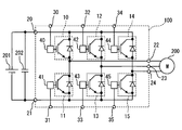
- FIG. 1 is a circuit diagram of the semiconductor device according to the first embodiment.
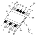
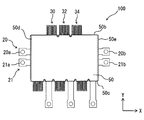
- FIG. 2 is a perspective view showing a schematic configuration of the semiconductor device shown in FIG.
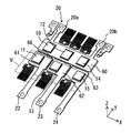
- FIG. 3 is a diagram in which the sealing portion and the insulating sheet are omitted from FIG. 2.
- FIG. 4 is a diagram in which a part of the heat sink is omitted from FIG.
- FIG. 5 is an enlarged view of a region V indicated by a broken line in FIG.
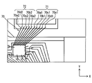
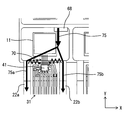
- FIG. 6 is an enlarged view of the periphery of the bonding wire in FIG.
- FIG. 7 is an equivalent circuit diagram for explaining the effect of suppressing malfunction, and corresponds to FIG. FIG.
- FIG. 8 is an enlarged view of the periphery of the bonding wire in the first modification.
- FIG. 9 is a perspective view illustrating a schematic configuration of a semiconductor device according to a second modification.
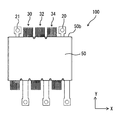
- FIG. 10 is a plan view showing a semiconductor device according to a third modification.
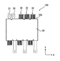
- FIG. 11 is a plan view showing a semiconductor device according to a fourth modification.
- FIG. 12 is a plan view showing a semiconductor device according to a fifth modification.
- FIG. 13 is a plan view showing a semiconductor device according to a sixth modification.
- FIG. 14 is a plan view showing a semiconductor device according to a seventh modification.
- FIG. 15 is a plan view illustrating a schematic configuration of the semiconductor device according to the second embodiment.
- FIG. 16 is a diagram in which some of the sealing portion, the insulating sheet, and the heat sink are omitted from FIG. 15.
- FIG. 17 is an enlarged view of a region XVII indicated by a broken line in FIG.
- FIG. 18 is an equivalent circuit diagram for explaining the effect of suppressing malfunction, and corresponds to FIG.
- FIG. 19 is a plan view showing a semiconductor device according to an eighth modification.
- FIG. 20 is a plan view showing a semiconductor device according to a ninth modification.
- symbol is provided to the part which is mutually the same or equivalent in each figure below.
- the thickness direction of the semiconductor chip is indicated as the Z direction.
- it is orthogonal to a Z direction and the extending direction of a control terminal is shown as a Y direction.
- a direction orthogonal to both the Y direction and the Z direction is referred to as an X direction.
- the planar shape indicates a shape along a plane defined by the X direction and the Y direction unless otherwise specified.
- the semiconductor device 100 includes upper and lower arms connected between a positive electrode (high potential side) and a negative electrode (low potential side) of a DC power supply 201 in order to drive a motor 200 as a load.
- a positive electrode high potential side
- a negative electrode low potential side
- the semiconductor device 100 is configured as a three-phase inverter, and converts DC power into three-phase AC and outputs it to the motor 200.
- Such a semiconductor device 100 is mounted on, for example, an electric vehicle or a hybrid vehicle.
- Reference numeral 202 shown in FIG. 1 is a smoothing capacitor.
- the semiconductor chip constituting each arm has a power switching element such as an IGBT or a MOSFET and an FWD element connected in antiparallel to the switching element.
- the power switching element and the FWD element may be configured in separate chips.
- the semiconductor device 100 includes six semiconductor chips 10 to 15 that employ n-channel IGBT elements as switching elements.
- the U-phase upper and lower arms are configured with the semiconductor chip 10 as the upper arm side and the semiconductor chip 11 as the lower arm side.
- the upper and lower arms of the V phase are configured with the semiconductor chip 12 as the upper arm side and the semiconductor chip 13 as the lower arm side.
- the upper and lower arms of the W phase are configured with the semiconductor chip 14 as the upper arm side and the semiconductor chip 15 as the lower arm side.
- the semiconductor device 100 includes a P terminal 20, an N terminal 21, output terminals 22 to 24, and control terminals 30 to 35 as terminals for external connection.
- the P terminal 20, the N terminal 21, and the output terminals 22 to 24 correspond to main terminals.
- the main terminal is also called a power terminal
- the control terminal is also called a signal terminal.
- the P terminal 20 is a terminal connected to the positive side of the DC power source 201, and the N terminal 21 is a terminal connected to the negative side of the DC power source.
- the P terminal 20 is electrically connected to the collector electrode of the IGBT element formed on the semiconductor chips 10, 12, and 14 on the upper arm side.
- the N terminal 21 is electrically connected to the emitter electrode of the IGBT element formed in the semiconductor chips 11, 13 and 15 on the lower arm side.
- the U-phase output terminal 22 is the emitter electrode of the IGBT element formed on the semiconductor chip 10 and the collector of the IGBT element formed on the semiconductor chip 11. It is electrically connected to the electrode.
- the V-phase output terminal 23 is electrically connected to the emitter electrode of the IGBT element formed on the semiconductor chip 12 and the collector electrode of the IGBT element formed on the semiconductor chip 13.
- the W-phase output terminal 24 is electrically connected to the emitter electrode of the IGBT element formed on the semiconductor chip 14 and the collector electrode of the IGBT element formed on the semiconductor chip 15.
- the collector electrode and emitter electrode of the semiconductor chips 10 to 15 correspond to the main electrode.
- the control terminals 30 to 35 are terminals for inputting or outputting various signals for controlling driving of elements formed in the semiconductor chips 10 to 15, and are electrically connected to control electrodes (pads) of the semiconductor chips 10 to 15. It is connected to the.
- the control terminal 30 corresponds to the semiconductor chip 10
- the control terminal 31 corresponds to the semiconductor chip 11.
- the control terminal 32 corresponds to the semiconductor chip 12
- the control terminal 33 corresponds to the semiconductor chip 13.
- the control terminal 34 corresponds to the semiconductor chip 14, and the control terminal 35 corresponds to the semiconductor chip 15.
- control terminals 30 to 35 are used for gate drive signals, for Kelvin emitters (for detecting the potential of the emitter electrode), for anode potentials of temperature sensitive diodes formed on the semiconductor chips 10 to 15, and also for cathode potentials. And a total of 5 for current sensing. In addition, there are two power supplies, five for error check, test mode setting, and gate potential check.
- the semiconductor device 100 includes driver ICs 40 to 45 in which drive circuits for controlling driving of elements formed in the corresponding semiconductor chips 10 to 15 are formed on the semiconductor chip.
- the driver ICs 40 to 45 generate analog signals such as gate drive signals based on control signals (digital signals) input from a microcomputer (not shown). Further, the detection value (analog value) of the above-described temperature sensitive diode or the like is converted into a digital signal and output.
- the driver ICs 40 to 45 correspond to driver chips.
- the semiconductor device 100 includes a sealing unit 50 that integrally seals the semiconductor chips 10 to 15.
- a 6-in-1 package is formed by sealing the six semiconductor chips 10 to 15 constituting the three-phase inverter by the sealing portion 50.
- the sealing part 50 is formed using, for example, a resin material. In this embodiment, it is formed by a transfer mold method using an epoxy resin.
- the sealing part 50 has a substantially rectangular plane shape, and one surface 50a in the Z direction and a surface opposite to the one surface 50a (not shown) are substantially flat. From these surfaces, heat radiating surfaces of heat sinks 60 to 67 described later are exposed.
- the insulating sheet 51 is affixed on the one surface 50a and the opposite surface so as to cover each heat radiation surface.
- the insulating sheet 51 electrically separates the semiconductor device 100 and the cooler from each other in a configuration in which coolers are disposed on both sides of the semiconductor device 100 in the Z direction, and heat radiation from both sides of the semiconductor device 100 is performed.
- the P terminal 20 (20a, 20b), the N terminal 21 (21a, 21b), and the semiconductor chips 10, 12, 14 on the upper arm side are provided.
- the control terminals 30, 32, and 34 corresponding to are projected.
- Each of the terminals 20, 21, 30, 32, 34 extends in the Y direction, and a part of the terminal protrudes from the side surface 50b.
- the ten terminals constituting each control terminal 30, 32, 34 are arranged side by side in the X direction, and the control terminals 30, 32, 34 are arranged in the X direction near the center of the side surface 50b. Is arranged in.
- the P terminal 20a and the N terminal 21a are arranged on one side in the X direction, and the P terminal 20b and the N terminal 21b are arranged on the other side so as to sandwich the control terminals 30, 32, and 34 therebetween. That is, the N terminal 21a, the P terminal 20a, the control terminal 30, the control terminal 32, the control terminal 34, the P terminal 20b, and the N terminal 21b are arranged in this order from one end side in the X direction.
- Each of the terminals 22 to 24, 31, 33, and 35 extends in the Y direction, and a part of the terminal protrudes from the side surface 50c.
- the ten terminals constituting each control terminal 31, 33, 35 are arranged side by side in the X direction.
- the control terminal 31, the output terminal 22, the control terminal 33, the output terminal 23, the control terminal 35, and the output terminal 24 are arranged in this order from one end side in the X direction.
- the output terminals 22 to 24 are the first main terminals
- the P terminal 20 and the N terminal 21 correspond to the second main terminal
- the side surface 50c corresponds to one surface of the sealing portion.
- the output terminals 22 to 24 correspond to the second main terminal
- the side surface 50b corresponds to one surface of the sealing portion.
- the X direction corresponds to the first direction.
- the semiconductor device 100 includes heat sinks 60 to 67 as shown in FIGS.
- the heat sinks 60 to 67 perform an electrical relay function between the corresponding P terminal 20, N terminal 21, output terminals 22 to 24 and the semiconductor chips 10 to 15, and radiate heat generated by the semiconductor chips 10 to 15. Fulfills the function.
- the heat sink 60 is formed integrally with the P terminal 20 (20a, 20b). On one surface of the heat sink 60, the semiconductor chips 10, 12, and 14 on the upper arm side are arranged with the collector electrode formation surfaces facing each other, and the respective collector electrodes are electrically connected to the heat sink 60.
- the heat sink 60 has a planar rectangular shape with the X direction as the longitudinal direction, and the semiconductor chips 10, 12, and 14 are arranged side by side in the X direction.
- the heat sink 61 is formed integrally with the U-phase output terminal 22.
- the semiconductor chip 11 is disposed with the collector electrode formation surface facing each other, and the collector electrode is electrically connected to the heat sink 61.
- the heat sink 62 is formed integrally with the V-phase output terminal 23.
- the semiconductor chip 13 is disposed with the collector electrode formation surface facing each other, and the collector electrode is electrically connected to the heat sink 62.
- the heat sink 63 is formed integrally with the W-phase output terminal 24.
- the semiconductor chip 15 is disposed with the collector electrode formation surface facing each other, and the collector electrode is electrically connected to the heat sink 63.
- the chip mounting surfaces of the heat sinks 60 to 63 described above are on the same side in the Z direction.
- the heat sinks 60 to 63 have substantially the same thickness, and the surface opposite to the chip mounting surface of each heat sink 60 to 63 is a heat dissipation surface exposed from the surface opposite to the one surface 50a of the sealing portion 50. .
- a heat sink 64 is disposed on the surface opposite to the heat sinks 61 to 63 of the semiconductor chips 11, 13, and 15.
- the heat sink 64 is electrically connected to the N terminal 21 (21a, 21b).
- the heat sink 64 has a planar rectangular shape whose longitudinal direction is the X direction, and is disposed across the semiconductor chips 11, 13, and 15.
- the heat sink 64 is electrically connected to the emitter electrodes of the semiconductor chips 11, 13 and 15.
- heat sinks 65 to 67 are arranged on the surface opposite to the heat sink 60 in the semiconductor chips 10, 12, and 14 on the upper arm side.
- the heat sink 65 is electrically connected to the emitter electrode of the semiconductor chip 10.
- the heat sink 66 is electrically connected to the emitter electrode of the semiconductor chip 12.
- the heat sink 67 is electrically connected to the emitter electrode of the semiconductor chip 14.
- Each of the heat sinks 65 to 67 is electrically connected to the corresponding heat sink 61 to 63.
- protrusions (not shown) are provided on the heat sinks 65 to 67, and the protrusions are connected to the connecting portions 68 of the heat sinks 61 to 63.
- the heat sinks 64 to 67 described above have substantially the same thickness, and the surface opposite to the semiconductor chips 10 to 15 in each of the heat sinks 64 to 67 is a heat dissipation surface exposed from the one surface 50a of the sealing portion 50. Yes. Further, as described above, the semiconductor chips 10 to 15 have a double-sided electrode structure having a collector electrode on one surface and an emitter electrode on the opposite surface.
- the semiconductor chip 11 is electrically connected to the corresponding driver IC 41 via the bonding wire 70.
- This bonding wire 70 corresponds to a relay member.
- the bonding wire 70 forms a signal path for controlling the driving of the elements formed on the semiconductor chip 11 together with the control terminal 31 described above.
- the plurality of signal paths connected to the semiconductor chip 11 are arranged in the X direction, and the U-phase output terminals 22 that are main terminals are arranged side by side with respect to the plurality of signal paths.
- the bonding wire 70 constitutes a first wire group 71 and a second wire group 72.
- the first wire group 71 corresponds to a first relay group
- the second wire group 72 corresponds to a second relay group.
- the first wire group 71 has five bonding wires 70a1 to 70e1.
- the bonding wire 70a1 is for the cathode potential of the temperature sensitive diode formed on the semiconductor chip 11, and the bonding wire 70b1 is for the anode potential.
- the bonding wire 70c1 is for the gate drive signal of the IGBT element, and the bonding wire 70d1 is for current sensing.
- the bonding wire 70e1 is for a Kelvin emitter that forms the reference potential (ground) of each signal path.
- the second wire group 72 has five bonding wires 70a2 to 70e2.
- the bonding wire 70a2 is for the cathode potential of the temperature sensitive diode formed on the semiconductor chip 11, and the bonding wire 70b2 is for the anode potential.
- the bonding wire 70c2 is for the gate drive signal of the IGBT element, and the bonding wire 70d2 is for current sensing.
- the bonding wire 70e2 is for the Kelvin emitter potential that forms the reference potential (ground) of each signal path.
- the bonding wires 70a1 and 70a2 are the bonding wires 70 having the same function. That is, it has five signal paths for the cathode potential of the temperature sensitive diode formed on the semiconductor chip 11, for the anode potential, for the gate drive signal of the IGBT element, for current sensing, and for the Kelvin emitter.
- the first signal path for the cathode potential, the second signal path for the anode potential, the third signal path for the gate drive signal, the fourth signal path for the current sense, and the fifth for the Kelvin emitter are also shown as signal path.
- the portion of the bonding wire 70 is branched into two.
- two electrodes (pads) of the semiconductor chip 11 and the driver IC 41 are also provided in each signal path.
- positioning of the X direction of the bonding wire 70 which has the same function becomes the positional relationship of mirror inversion in the 1st wire group 71 and the 2nd wire group 72.
- FIG. 6 The bonding wires 70a1 to 70e1 constituting the first wire group 71 are arranged side by side in the X direction. Specifically, the bonding wire 70a1, the bonding wire 70b1, the bonding wire 70c1, the bonding wire 70d1, and the bonding wire 70e1 are arranged in this order.
- bonding wires 70a2 to 70e2 constituting the second wire group 72 are also arranged side by side in the X direction. Further, the second wire group 72 is disposed next to the first wire group 71.
- the bonding wire 70a2 is disposed next to the bonding wire 70a1.
- the bonding wire 70a2, the bonding wire 70b2, the bonding wire 70c2, the bonding wire 70d2, and the bonding wire 70e2 are arranged in this order in the direction away from the bonding wire 70a1.
- the driver IC 41 and the control terminal 31 are electrically connected via the bonding wire 73.
- a passive component 74 such as a chip resistor or a chip capacitor is mounted so as to straddle some control terminals 31.
- the semiconductor device 100 includes the driver IC 41. Therefore, among the signal paths described above, a digital signal is transmitted to the control terminal 31 and an analog signal is transmitted to the bonding wire 70.
- the self-inductance is sufficiently larger in the bonding wire 70 through which the analog signal flows than in the control terminal 31. Therefore, the self-inductance of the bonding wire 70 may be taken into consideration when considering the mutual inductance with the output terminals 22 arranged in parallel. Note that even if noise is superimposed on the digital signal at the control terminal 31, malfunction does not easily occur. However, if noise is superimposed on the analog signal on the bonding wire 70, malfunction is likely to occur.
- the noise voltage is determined by the product of the mutual inductance of each signal path and the time change di / dt of the energization current. For example, if di / dt is 2 kA / ⁇ s and the mutual inductance is 1 nH, noise of 2 V is generated.
- the five signal paths are branched into two at the bonding wire 70 portion. That is, the bonding wires 70 having the same function are provided in pairs.
- the first wire group 71 including one of the paired bonding wires 70 and the second wire group 72 including the other are arranged adjacent to each other in the X direction, and the arrangement order is in a mirror inversion relationship. ing.
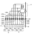
- FIG. 7 shows an equivalent circuit diagram of the configuration shown in FIGS.
- the first wire group 71 and the second wire group 72 are arranged in this order from the output terminal 22 side.
- the bonding wire 70a1, the bonding wire 70a2, the bonding wire 70b2, the bonding wire 70c2, the bonding wire 70d2, and the bonding wire 70e2 are arranged in this order.
- L22 represents the self-inductance of the output terminal 22.
- L70a1, L70b1, L70c1, L70d1, and L70e1 indicate the self-inductances of the bonding wire 70a1, the bonding wire 70b1, the bonding wire 70c1, the bonding wire 70d1, and the bonding wire 70e1, respectively.
- L70a2, L70b2, L70c2, L70d2, and L70e2 indicate the self-inductances of the bonding wire 70a2, the bonding wire 70b2, the bonding wire 70c2, the bonding wire 70d2, and the bonding wire 70e2, respectively.
- the bonding wire 70e1 constituting the fifth signal path for the Kelvin emitter that becomes the reference potential of each signal path is closest to the output terminal 22, and the bonding wire 70e2 is farthest. Therefore, the mutual inductance between the bonding wire 70e1 and the output terminal 22 is large, and the mutual inductance between the bonding wire 70e2 and the output terminal 22 is small. As a result, the combined mutual inductance, that is, the mutual inductance of the fifth signal path is approximately an intermediate value of each mutual inductance.
- the bonding wire 70d1 constituting the fourth signal path is second closest to the output terminal 22, and the bonding wire 70d2 is second farthest. Therefore, the mutual inductance (synthetic mutual inductance) of the fourth signal path is substantially equal to the mutual inductance of the fifth signal path.
- the bonding wire 70c1 constituting the third signal path is third closest to the output terminal 22, and the bonding wire 70c2 is third farthest. Therefore, the mutual inductance (synthetic mutual inductance) of the third signal path is also substantially equal to the mutual inductance of the fifth signal path.
- the bonding wire 70b1 constituting the second signal path is fourth closest to the output terminal 22, and the bonding wire 70b2 is fourth farthest. Therefore, the mutual inductance (synthetic mutual inductance) of the second signal path is also substantially equal to the mutual inductance of the fifth signal path.
- the bonding wire 70a1 constituting the first signal path is the fifth closest to the output terminal 22, and the bonding wire 70a2 is the fifth furthest. Therefore, the mutual inductance (synthetic mutual inductance) of the first signal path is also substantially equal to the mutual inductance of the fifth signal path.
- the combined inductances of the five signal paths are substantially equal. Therefore, even if the large current 75 flows instantaneously, the noise voltage generated in each signal path becomes substantially equal. For this reason, even if noise is superimposed, the potential difference of each signal path with reference to the Kelvin emitter potential is hardly changed. Therefore, malfunction of the semiconductor chip 11 and the driver IC 41 due to noise can be suppressed.
- the P terminal 20, the N terminal 21, and the control terminals 30, 32, and 34 protrude from the side surface 50b of the sealing portion 50 and extend in a direction orthogonal to the Z direction, so that the output terminals 22 to 24 and control terminals 31, 33, and 35 project from the opposite side surface 50c and extend in a direction orthogonal to the Z direction. Therefore, the physique can be reduced in size in the Z direction. Further, the heat of the semiconductor device 100 can be radiated to both sides in the Z direction. In particular, in the present embodiment, since the heat dissipation surfaces of the heat sinks 60 to 67 are exposed, heat dissipation can be improved while suppressing malfunction due to noise.
- the bonding wires 70 are paired with the same function for all six arms.
- the bonding wires 70 may be paired with the same function only on a part of the six arms, for example, only on the lower arm side.
- a first modification shown in FIG. 8 corresponds to FIG. 6 and shows a U-phase lower arm.
- an analog signal also flows through the control terminal 31, and therefore the self-inductance is taken into consideration including the control terminal 31.
- the control terminal 31 is also branched into two, and a first terminal group 36 and a second terminal group 37 are configured.
- the first terminal group 36 includes control terminals 31a1, 31b1, 31c1, 31d1, and 31e1.
- the second terminal group 37 includes control terminals 31a2, 31b2, 31c2, 31d2, and 31e2.
- control terminals 31a1 and 31a2 are for the cathode potential of the temperature sensitive diode
- bonding wire 70a1 is connected to the control terminal 31a1
- the bonding wire 70a2 is connected to the control terminal 31a2.
- Other explanations are omitted.
- the arrangement of signal paths in the X direction is the same as the arrangement of the bonding wires 70 described above.
- the output terminal 22 which is a main terminal is arrange
- the lower arm side of the U phase has been described as an example, but other arms can be similarly configured.
- the above embodiment is applied even in a configuration in which the heat radiation surfaces of the heat sinks 60 to 67 are not exposed from the sealing portion 50, in other words, in a configuration in which the insulating sheet 51 is not attached. be able to. Further, the present invention can be applied to a configuration in which only the heat radiating surfaces of the heat sinks 60 to 63 are exposed and a configuration in which only the heat radiating surfaces of the heat sinks 64 to 67 are exposed.
- the arrangement of the P terminal 20 and the N terminal 21 which are main terminals is not limited to the above example.
- the P terminal 20 and the N terminal 21 may be arranged together on one side of the control terminals 30, 32, 34 in the X direction.
- the P terminal 20 and the N terminal 21 may be arranged on side surfaces 50d and 50e different from the side surfaces 50b and 50c provided with the control terminals 30 to 35.
- the P terminal 20 and the N terminal 21 form a pair, one terminal 20a, 21a is disposed on the side surface 50d, and the other terminal 20b, 21b is disposed on the side surface 50e opposite to the side surface 50d.
- the above embodiment can be applied to the semiconductor device 100 other than the 6-in-1 package.
- the semiconductor device 100 is a 2-in-1 package having upper and lower arms for only one phase.
- a semiconductor device 100 that forms a U-phase arm is illustrated.
- the P terminal 20 and the N terminal 21 protrude from the side surface 50b of the sealing part 50, and the output terminal 22 and the control terminals 30 and 31 protrude from the opposite side surface 50c.
- the above-mentioned structure is employ
- a configuration in which the control terminals 30 and 31 are provided on the side surface 50b side may be employed.
- the semiconductor device 100 is a 1 in 1 package having only one arm.
- a semiconductor device 100 that forms a U-phase upper arm is illustrated.
- the P terminal 20 protrudes from the side surface 50b of the sealing part 50, and the output terminal 22 and the control terminal 30 protrude from the opposite side surface 50c.
- a configuration in which the control terminal 30 is provided on the side surface 50b side may be employed.
- output terminals 22 to 24 are provided in pairs.
- the U-phase output terminal 22 is branched and has two output terminals 22a and 22b.
- the U-phase control terminal 31, that is, the signal path including the control terminal 31 is disposed on both sides of the signal path of the U-phase lower arm.
- the V-phase output terminal 23 is branched and has two output terminals 23a and 23b.
- the V-phase control terminal 33 that is, the signal path including the control terminal 33 is disposed on both sides of the signal path of the V-phase lower arm.
- the W-phase output terminal 24 is branched and has two output terminals 24a and 24b.
- the W-phase control terminal 35 that is, the signal path including the control terminal 35 is disposed on both sides of the signal path of the W-phase lower arm.
- Each of the output terminals 22 to 24 is substantially U-shaped.
- the P terminal 20 and the N terminal 21 are paired as in the first embodiment.
- the bonding wires 70 are not provided in pairs as illustrated in the U-phase lower arm in FIG. 17, and there is one bonding wire 70 for each signal path. Other configurations are the same as those in the first embodiment.
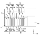
- FIG. 18 shows an equivalent circuit diagram of the configuration shown in FIG.
- the semiconductor device 100 includes the driver IC 41. Therefore, as shown in the first embodiment, the self-inductance of the bonding wire 70 may be taken into consideration when considering the mutual inductance between the signal path and the output terminal 22.
- the bonding wire 70a, the bonding wire 70b, the bonding wire 70c, the bonding wire 70d, and the bonding wire 70e are arranged in this order from the output terminal 22a side.
- the bonding wire 70a is for the cathode potential of the temperature sensitive diode formed on the semiconductor chip 11, and the bonding wire 70b is for the anode potential.
- the bonding wire 70c is for the gate drive signal of the IGBT element, and the bonding wire 70d is for current sensing.
- the bonding wire 70e is for a Kelvin emitter that forms a reference potential (ground) of each signal path.
- L22a indicates the self-inductance of the output terminal 22a
- L22b indicates the self-inductance of the output terminal 22b
- L70a, L70b, L70c, L70d, and L70e indicate self-inductances of the bonding wire 70a, the bonding wire 70b, the bonding wire 70c, the bonding wire 70d, and the bonding wire 70e, respectively.
- the bonding wire 70e constituting the fifth signal path for the Kelvin emitter, which serves as the reference potential for each signal path, is farthest from the output terminal 22a and closest to the output terminal 22b. Therefore, the mutual inductance between the bonding wire 70e and the output terminal 22a is small, and the mutual inductance between the bonding wire 70e and the output terminal 22b is large. As a result, the combined mutual inductance, that is, the mutual inductance of the fifth signal path is approximately an intermediate value of each mutual inductance.
- the bonding wire 70d constituting the fourth signal path is second farthest from the output terminal 22a and second closest to the output terminal 22b. Therefore, the mutual inductance (synthetic mutual inductance) of the fourth signal path is substantially equal to the mutual inductance of the fifth signal path.
- the bonding wire 70c constituting the third signal path is the third farthest from the output terminal 22a and the third closest to the output terminal 22b. Therefore, the mutual inductance (synthetic mutual inductance) of the third signal path is also substantially equal to the mutual inductance of the fifth signal path.
- the bonding wire 70b constituting the second signal path is second closest to the output terminal 22a and second closest to the output terminal 22b. Therefore, the mutual inductance (synthetic mutual inductance) of the second signal path is also substantially equal to the mutual inductance of the fifth signal path.
- the bonding wire 70a constituting the first signal path is closest to the output terminal 22a and is farthest from the output terminal 22b. Therefore, the mutual inductance (synthetic mutual inductance) of the first signal path is also substantially equal to the mutual inductance of the fifth signal path.
- the combined inductances of the five signal paths are substantially equal. Therefore, even if the large current 75 flows instantaneously, the noise voltage generated in each signal path becomes substantially equal. For this reason, even if noise is superimposed, the potential difference of each signal path with reference to the Kelvin emitter potential is hardly changed. Therefore, malfunction of the semiconductor chip 11 and the driver IC 41 due to noise can be suppressed.
- the P terminal 20, the N terminal 21, and the control terminals 30, 32, 34 protrude from the side surface 50 b of the sealing portion 50 and extend in a direction perpendicular to the Z direction, and the output terminal 22.
- To 24 and the control terminals 31, 33, and 35 protrude from the opposite side surface 50c and extend in a direction orthogonal to the Z direction. Therefore, the physique can be reduced in size in the Z direction. Further, the heat of the semiconductor device 100 can be radiated to both sides in the Z direction. In particular, in the present embodiment, since the heat dissipation surfaces of the heat sinks 60 to 67 are exposed, heat dissipation can be improved while suppressing malfunction due to noise.
- the output terminals 22 to 24 have a substantially U-shaped branch structure, like the P terminal 20 and the N terminal 21, they may be divided into two. On the contrary, the P terminal 20 and the N terminal 21 may have a branch structure like the output terminals 22 to 24.
- the arrangement of the P terminal 20 and the N terminal 21 is not limited. Further, the present invention can be applied to a configuration in which all the heat dissipation surfaces of the heat sinks 60 to 67 are not exposed, a configuration in which only the heat dissipation surfaces of the heat sinks 60 to 63 are exposed, and a configuration in which only the heat dissipation surfaces of the heat sinks 64 to 67 are exposed. .
- the configuration of the semiconductor device 100 is not limited to the 6 in 1 package.
- the present invention can also be applied to a 2 in 1 package and a 1 in 1 package.
- the semiconductor device 100 is a 2-in-1 package having upper and lower arms for only one phase.
- FIG. 19 shows a semiconductor device 100 that forms a U-phase arm as an example.
- the P terminal 20 and the N terminal 21 protrude from the side surface 50b of the sealing part 50, and the output terminal 22 and the control terminals 30 and 31 protrude from the opposite side surface 50c.
- a pair of output terminals 22 a and 22 b are arranged on both sides of the control terminal 30, and a pair of output terminals 22 b and 22 c are arranged on both sides of the control terminal 31.
- the output terminal 22b is also used as the control terminals 30 and 31.
- it can also be set as the structure which has only output terminal 22a, 22c.
- the distance between the signal path and the output terminals 22a and 22b is biased. Therefore, in the X direction, it is preferable that the centers of the paired output terminals 22a and 22b coincide with the center of the signal path.
- control terminals 30 and 31 may be arranged between the P terminal 20 and the N terminal 21 and the P terminal 20 and the N terminal 21 may be paired.
- FIG. 19 shows an example in which the driver ICs 40 and 41 are not provided and the number of control terminals 30 and 31 is five. However, it goes without saying that the driver ICs 40 and 41 may be provided.
- the semiconductor device 100 is a 1 in 1 package having only one arm.
- a semiconductor device 100 that forms a U-phase upper arm is shown.
- the P terminal 20 protrudes from the side surface 50b of the sealing part 50, and the output terminal 22 and the control terminal 30 protrude from the opposite side surface 50c.
- the output terminal 22 has a pair of output terminals 22a and 22b, and a signal path including the control terminal 30 is disposed between the output terminals 22a and 22b.
- the control terminal 30 may be provided on the side surface 50b side and the P terminal 20 may be paired.
- FIG. 20 shows an example in which the driver IC 40 is not provided and the number of control terminals 30 is five. However, it goes without saying that a configuration including the driver IC 40 may be used.
- the example of the bonding wire 70 was shown as a relay member, it is not limited to this. Any member that electrically relays the driver ICs 40 to 45 corresponding to the semiconductor chips 10 to 15 or the control terminals 30 to 35 corresponding to the semiconductor chips 10 to 15 can be adopted.
- side surfaces 50b and 50c was shown as one surface of the sealing part 50, it is not limited to a side surface.
Landscapes
- Engineering & Computer Science (AREA)
- Power Engineering (AREA)
- Inverter Devices (AREA)
- Lead Frames For Integrated Circuits (AREA)
- Microelectronics & Electronic Packaging (AREA)
Abstract
半導体装置(100)において、主端子(22)及び同一の半導体チップ(11)に対応する複数の制御端子(31)が封止部(50)の一面(50c)から突出し、複数の前記制御端子を含む複数の信号経路が前記主端子と第1方向に並んで配置される。複数の前記信号経路において、同じ機能の中継部材がそれぞれ対で設けられ、対をなす前記中継部材の一方を含む第1中継群(71)と、他方を含む第2中継群(72)とが、前記第1方向において隣り合って配置されるとともに、前記第1中継群と前記第2中継群との並び順がミラー反転の関係となっている。
Description
本開示は、2014年3月26日に出願された日本出願番号2014-64195号に基づくもので、ここにその記載内容を援用する。
本開示は、半導体装置に関する。
従来、主端子及び同一の半導体チップに対応する複数の制御端子が封止部の一面から突出し、該制御端子を含む信号経路が第1方向に並んで配置されるとともに、第1方向において主端子が信号経路に並んで配置された半導体装置として、特許文献1に記載のものが知られている。
特許文献1に記載の半導体装置は、三相インバータを構成するための6つの半導体素子(半導体チップ)を有している。この半導体チップのコレクタ電極及びエミッタ電極には、配線部材(主端子)が接続されている。一方、ゲート電極には、ボンディングワイヤ(中継部材)を介して配線部材(制御端子)が接続されている。これら主端子及び制御端子は、樹脂モールド部(封止部)から突出している。
また、例えば各相の出力用の主端子と各相の制御端子とが、封止部の同一面から突出しており、制御端子が並ぶ第1方向において、相ごとに、制御端子と主端子が並んで配置されている。
上記したように、制御端子は、中継部材を介して制御電極と電気的に接続されており、中継部材及び制御端子を含んで信号経路が形成されている。すなわち、第1方向において、複数の信号経路と主端子が並んで配置されている。
このような構成では、短絡が生じて、制御端子に並設された主端子と、別の主端子との間に瞬間的に大電流が流れると、並設された主端子と信号経路との磁気結合によってノイズが発生し、信号経路をノイズが伝搬して誤動作が生じる虞がある。
本開示の目的は、短絡発生時のノイズによる誤動作を抑制することができる半導体装置を提供することである。
本開示の一態様に係る半導体装置は、少なくともひとつの半導体チップと、封止部と、複数の主端子と、複数の中継部材と、複数の制御端子と、を備える。前記半導体チップは、スイッチング素子が形成され、対をなす主電極と複数の制御電極とを有する。前記封止部は、前記半導体チップを封止する。複数の前記主端子は、前記主電極に電気的に接続され、前記封止部から突出する。複数の前記中継部材は、前記制御電極にそれぞれ接続される。複数の前記制御端子は、前記中継部材を介して前記制御電極に電気的に接続され、対応する前記中継部材とともに信号経路をなし、前記封止部から突出する。複数の前記主端子が、前記封止部の一面から突出する第1主端子と、前記一面とは別の面から突出する第2主端子とを有する。同一の前記半導体チップに対応する複数の前記制御端子が前記一面から突出し、前記制御端子を含む前記信号経路が第1方向に並んで配置されるとともに、前記第1方向において前記第1主端子が前記信号経路に並んで配置されている。
前記第1主端子に並んで配置された複数の前記信号経路において、同じ機能の前記中継部材がそれぞれ対で設けられる。対をなす前記中継部材の一方を含む第1中継群と、他方を含む第2中継群とが、第1方向において隣り合って配置されるとともに、前記第1中継群と前記第2中継群との並び順がミラー反転の関係となっている。
ノイズによる誤動作は、各信号経路に生じるノイズ自体の絶対的な大きさによるのではなく、並設された各信号経路においてノイズ電圧の差が大きいと生じる。前記半導体装置によれば、対をなす前記中継部材の一方と前記第1主端子の相互インダクタンスと、前記中継部材の他方と前記第1主端子の相互インダクタンスとを合成した相互インダクタンスが、各信号経路でほぼ等しくなる。したがって、短絡が生じて第1主端子と第2主端子との間に瞬間的に大電流が流れても、ノイズによる誤動作を抑制することができる。
本開示の別の態様に係る半導体装置は、少なくともひとつの半導体チップと、封止部と、複数の主端子と、複数の中継部材と、複数の制御端子とを備える。前記半導体チップは、スイッチング素子が形成され、対をなす主電極と複数の制御電極とを有する。前記封止部は、前記半導体チップを封止する。複数の前記主端子は、前記主電極に電気的に接続され、前記封止部から突出する。複数の前記中継部材は、前記制御電極にそれぞれ接続される。複数の前記制御端子は、前記中継部材を介して前記制御電極に電気的に接続され、対応する前記中継部材とともに信号経路をなし、前記封止部から突出する。複数の前記主端子が、前記封止部の一面から突出する第1主端子と、前記一面とは別の面から突出する第2主端子と、を有する。同一の前記半導体チップに対応する複数の前記制御端子が前記一面から突出し、前記制御端子を含む前記信号経路が第1方向に並んで配置されるとともに、前記第1方向において前記第1主端子が前記信号経路に並んで配置されている。同じ機能の前記第1主端子が対で設けられ、対をなす前記第1主端子が、前記第1方向において、複数の前記信号経路を間に挟むように、複数の前記信号経路の両側に配置されている。
上記したように、ノイズによる誤動作は、各信号経路に生じるノイズ自体の絶対的な大きさによるのではなく、並設された各信号経路においてノイズ電圧の差が大きいと生じる。前記半導体装置によれば、対をなす前記第1主端子の一方と前記信号経路の相互インダクタンスと、前記第1主端子の他方と前記信号経路の相互インダクタンスとを合成した相互インダクタンスが、各信号経路でほぼ等しくなる。したがって、短絡が生じて前記第1主端子と前記第2主端子との間に瞬間的に大電流が流れても、ノイズによる誤動作を抑制することができる。
本開示における上記あるいは他の目的、構成、利点は、下記の図面を参照しながら、以下の詳細説明から、より明白となる。図面において、
図1は、第1実施形態に係る半導体装置の回路図である。
図2は、図1に示す半導体装置の概略構成を示す斜視図である。
図3は、図2において、封止部及び絶縁シートを省略した図である。
図4は、図3において、ヒートシンクの一部を省略した図である。
図5は、図4に破線で示す領域Vを拡大した図である。
図6は、図5においてボンディングワイヤ周辺を拡大した図である。
図7は、誤動作抑制の効果を説明するための等価回路図であり、図5に対応している。
図8は、第1変形例におけるボンディングワイヤ周辺を拡大した図である。
図9は、第2変形例に係る半導体装置の概略構成を示す斜視図である。
図10は、第3変形例に係る半導体装置を示す平面図である。
図11は、第4変形例に係る半導体装置を示す平面図である。
図12は、第5変形例に係る半導体装置を示す平面図である。
図13は、第6変形例に係る半導体装置を示す平面図である。
図14は、第7変形例に係る半導体装置を示す平面図である。
図15は、第2実施形態に係る半導体装置の概略構成を示す平面図である。
図16は、図15において、封止部、絶縁シート、及びヒートシンクの一部を省略した図である。
図17は、図16に破線で示す領域XVIIを拡大した図である。
図18は、誤動作抑制の効果を説明するための等価回路図であり、図17に対応している。
図19は、第8変形例に係る半導体装置を示す平面図である。
図20は、第9変形例に係る半導体装置を示す平面図である。
以下、本開示の実施形態を、図面を参照して説明する。なお、以下の各図相互において互いに同一もしくは均等である部分に、同一符号を付与する。また、半導体チップの厚み方向をZ方向と示す。また、Z方向に直交し、制御端子の延設方向をY方向と示す。また、Y方向及びZ方向の両方向に直交する方向をX方向と示す。また、平面形状とは、特に断わりのない限り、X方向及びY方向により規定される面に沿う形状を示す。
(第1実施形態)
先ず、図1~図6に基づき、本実施形態に係る半導体装置100の構成について説明する。
先ず、図1~図6に基づき、本実施形態に係る半導体装置100の構成について説明する。
図1に示すように、半導体装置100は、負荷としてのモータ200を駆動するために、直流電源201の正極(高電位側)と負極(低電位側)との間に接続された上下アームを三相分有している。このように、半導体装置100は三相インバータとして構成されており、直流電力を三相交流に変換し、モータ200に出力する。このような半導体装置100は、例えば電気自動車やハイブリッド車に搭載される。なお、図1に示す符号202は、平滑用のコンデンサである。
各アームを構成する半導体チップは、IGBTやMOSFETなどのパワー系スイッチング素子と該スイッチング素子に逆並列に接続されたFWD素子とを有している。なお、パワー系スイッチング素子とFWD素子とを別チップに構成することもできる。本実施形態では、半導体装置100が、スイッチング素子としてnチャネル型のIGBT素子を採用した6つの半導体チップ10~15を備えている。そして、半導体チップ10を上アーム側、半導体チップ11を下アーム側として、U相の上下アームが構成されている。同じく、半導体チップ12を上アーム側、半導体チップ13を下アーム側として、V相の上下アームが構成されている。半導体チップ14を上アーム側、半導体チップ15を下アーム側として、W相の上下アームが構成されている。
また、半導体装置100は、外部接続用の端子として、P端子20、N端子21、出力端子22~24、及び制御端子30~35を備えている。このうち、P端子20、N端子21、及び出力端子22~24が、主端子に相当する。なお、主端子はパワー端子、制御端子は信号端子とも呼ばれる。
P端子20は、直流電源201の正極側に接続される端子であり、N端子21は直流電源の負極側に接続される端子である。P端子20は、上アーム側の半導体チップ10,12,14に形成されたIGBT素子のコレクタ電極に、電気的に接続されている。N端子21は、下アーム側の半導体チップ11,13,15に形成されたIGBT素子のエミッタ電極に、電気的に接続されている。
モータ200の三相線に接続される出力端子22~24のうち、U相の出力端子22は、半導体チップ10に形成されたIGBT素子のエミッタ電極及び半導体チップ11に形成されたIGBT素子のコレクタ電極に、電気的に接続されている。同じく、V相の出力端子23は、半導体チップ12に形成されたIGBT素子のエミッタ電極及び半導体チップ13に形成されたIGBT素子のコレクタ電極に、電気的に接続されている。W相の出力端子24は、半導体チップ14に形成されたIGBT素子のエミッタ電極及び半導体チップ15に形成されたIGBT素子のコレクタ電極に、電気的に接続されている。なお、半導体チップ10~15のコレクタ電極及びエミッタ電極が主電極に相当する。
制御端子30~35は、半導体チップ10~15に形成された素子の駆動を制御するための各種信号を、入力または出力する端子であり、半導体チップ10~15の制御電極(パッド)に電気的に接続されている。制御端子30は半導体チップ10に対応し、制御端子31は半導体チップ11に対応している。同じく、制御端子32は半導体チップ12に対応し、制御端子33は半導体チップ13に対応している。制御端子34は半導体チップ14に対応し、制御端子35は半導体チップ15に対応している。
本実施形態では、各制御端子30~35が、ゲート駆動信号用、ケルビンエミッタ用(エミッタ電極の電位検出用)、半導体チップ10~15に形成された感温ダイオードのアノード電位用、同じくカソード電位用、電流センス用の計5本を有している。加えて、電源用が2本、エラーチェック用、テストモード設定用、ゲート電位チェック用の計5本を有している。
また、半導体装置100は、半導体チップに、対応する半導体チップ10~15に形成された素子の駆動を制御するためのドライブ回路が形成されてなるドライバIC40~45を有している。このドライバIC40~45は、図示しないマイコンから入力される制御信号(デジタル信号)に基づいて、ゲート駆動信号などのアナログ信号を生成する。また、上記した感温ダイオードなどの検出値(アナログ値)をデジタル信号に変換して出力する。なお、ドライバIC40~45が、ドライバチップに相当する。
図2に示すように、半導体装置100は、半導体チップ10~15を一体的に封止する封止部50を備えている。このように、三相インバータを構成する6つの半導体チップ10~15が封止部50によって封止されてなる6in1パッケージとなっている。
封止部50は、例えば、樹脂材料を用いて形成されている。本実施形態では、エポキシ樹脂を用いたトランスファモールド法により形成されている。封止部50は、平面略矩形状をなしており、Z方向における一面50aと、図示しない一面50aと反対の面とがほぼ平坦となっている。そして、これらの面から、後述するヒートシンク60~67の放熱面が露出されている。
一面50a及びその反対の面には、各放熱面を被覆するように、絶縁シート51が貼り付けられている。この絶縁シート51は、Z方向において半導体装置100の両側に冷却器が配置され、半導体装置100から両面放熱がなされる構成において、半導体装置100と冷却器との間を電気的に分離する。
一面50a及びその反対の面を繋ぐ側面のうち、側面50bからは、上記したP端子20(20a,20b)、N端子21(21a,21b)、及び上アーム側の半導体チップ10,12,14に対応する制御端子30,32,34が突出している。各端子20,21,30,32,34はY方向に延設されており、その一部が側面50bから突出している。また、各制御端子30,32,34を構成する10本の端子は、それぞれX方向に並んで配置されており、側面50bの中央付近に、制御端子30,32,34同士がX方向に並んで配置されている。そして、これら制御端子30,32,34を間に挟むように、X方向の一方側にP端子20a及びN端子21a、他方側にP端子20b及びN端子21bが配置されている。すなわち、X方向の一端側から、N端子21a、P端子20a、制御端子30、制御端子32、制御端子34、P端子20b、N端子21bの順に配置されている。
一方、側面50bと反対の側面50cからは、上記した出力端子22~24、及び、下アーム側の半導体チップ11,13,15に対応する制御端子31,33,35が突出している。各端子22~24,31,33,35はY方向に延設されており、その一部が側面50cから突出している。また、各制御端子31,33,35を構成する10本の端子は、それぞれX方向に並んで配置されている。そして、X方向の一端側から、制御端子31、出力端子22、制御端子33、出力端子23、制御端子35、出力端子24の順に配置されている。例えば、出力端子22~24が第1主端子とすると、P端子20及びN端子21が第2主端子に相当し、側面50cが封止部の一面に相当する。逆に、P端子20又はN端子21が第1主端子とすると、出力端子22~24が第2主端子に相当し、側面50bが封止部の一面に相当する。また、X方向が、第1方向に相当する。
半導体装置100は、図3及び図4に示すように、ヒートシンク60~67を備えている。ヒートシンク60~67は、対応するP端子20、N端子21、出力端子22~24と半導体チップ10~15との電気的な中継機能を果たすとともに、半導体チップ10~15が生じた熱を放熱する機能を果たす。
ヒートシンク60は、P端子20(20a,20b)と一体的に形成されている。ヒートシンク60の一面には、上アーム側の半導体チップ10,12,14がコレクタ電極形成面を対向させて配置され、ヒートシンク60にそれぞれのコレクタ電極が電気的に接続されている。ヒートシンク60はX方向を長手とする平面矩形状をなしており、半導体チップ10,12,14は、X方向に並んで配置されている。
一方、下アーム側の半導体チップ11,13,15は、それぞれヒートシンク61~63上に配置されている。ヒートシンク61は、U相の出力端子22と一体的に形成されている。ヒートシンク61の一面上には、半導体チップ11がコレクタ電極形成面を対向させて配置され、ヒートシンク61にコレクタ電極が電気的に接続されている。ヒートシンク62は、V相の出力端子23と一体的に形成されている。ヒートシンク62の一面上には、半導体チップ13がコレクタ電極形成面を対向させて配置され、ヒートシンク62にコレクタ電極が電気的に接続されている。ヒートシンク63は、W相の出力端子24と一体的に形成されている。ヒートシンク63の一面上には、半導体チップ15がコレクタ電極形成面を対向させて配置され、ヒートシンク63にコレクタ電極が電気的に接続されている。なお、上記したヒートシンク60~63におけるチップ搭載面は、Z方向において同じ側である。各ヒートシンク60~63はほぼ同じ厚みを有しており、各ヒートシンク60~63におけるチップ搭載面と反対の面が、封止部50における一面50aと反対の面から露出する放熱面となっている。
半導体チップ11,13,15におけるヒートシンク61~63と反対の面上には、ヒートシンク64が配置されている。ヒートシンク64は、N端子21(21a,21b)に電気的に接続されている。ヒートシンク64はX方向を長手とする平面矩形状をなしており、半導体チップ11,13,15を跨いで配置されている。このヒートシンク64は、半導体チップ11,13,15のエミッタ電極と電気的に接続されている。
一方、上アーム側の半導体チップ10,12,14におけるヒートシンク60と反対の面上には、ヒートシンク65~67が配置されている。ヒートシンク65は、半導体チップ10のエミッタ電極と電気的に接続されている。ヒートシンク66は、半導体チップ12のエミッタ電極と電気的に接続されている。ヒートシンク67は、半導体チップ14のエミッタ電極と電気的に接続されている。各ヒートシンク65~67は、対応する相のヒートシンク61~63と電気的に接続されている。本実施形態では、図示しない突出部がヒートシンク65~67に設けられ、この突出部がヒートシンク61~63の連結部68に接続されている。
なお、上記したヒートシンク64~67はほぼ同じ厚みを有しており、各ヒートシンク64~67における半導体チップ10~15と反対の面が、封止部50における一面50aから露出する放熱面となっている。また、上記したように、半導体チップ10~15は、一面にコレクタ電極を有し、一面と反対の面にエミッタ電極を有する両面電極構造をなしている。
図5及び図6では、U相の下アーム側を例示している。以下、U相下アームについて説明するが、他のアームについても同様の構成となっている。半導体チップ11は、ボンディングワイヤ70を介して、対応するドライバIC41と電気的に接続されている。このボンディングワイヤ70が、中継部材に相当する。
ボンディングワイヤ70は、上記した制御端子31とともに、半導体チップ11に形成された素子の駆動を制御するための信号経路をなしている。そして、半導体チップ11に接続された複数の信号経路はX方向に並んでおり、複数の信号経路に対し、主端子であるU相の出力端子22が並んで配置されている。
本実施形態では、ボンディングワイヤ70により、第1ワイヤ群71と、第2ワイヤ群72と、が構成されている。この第1ワイヤ群71が、第1中継群に相当し、第2ワイヤ群72が、第2中継群に相当する。
第1ワイヤ群71は、5本のボンディングワイヤ70a1~70e1を有している。ボンディングワイヤ70a1は、半導体チップ11に形成された感温ダイオードのカソード電位用であり、ボンディングワイヤ70b1は、アノード電位用である。ボンディングワイヤ70c1は、IGBT素子のゲート駆動信号用であり、ボンディングワイヤ70d1は、電流センス用である。ボンディングワイヤ70e1は、各信号経路の基準電位(グランド)をなすケルビンエミッタ用である。
第2ワイヤ群72は、5本のボンディングワイヤ70a2~70e2を有している。ボンディングワイヤ70a2は、半導体チップ11に形成された感温ダイオードのカソード電位用であり、ボンディングワイヤ70b2は、アノード電位用である。ボンディングワイヤ70c2は、IGBT素子のゲート駆動信号用であり、ボンディングワイヤ70d2は、電流センス用である。ボンディングワイヤ70e2は、各信号経路の基準電位(グランド)をなすケルビンエミッタ電位用である。
このように、第1ワイヤ群71と第2ワイヤ群72とでボンディングワイヤ70が同数とされ、且つ、同じ機能のボンディングワイヤ70がそれぞれ設けられている。例えば、ボンディングワイヤ70a1,70a2が、同じ機能を有するボンディングワイヤ70である。すなわち、半導体チップ11に形成された感温ダイオードのカソード電位用、アノード電位用、IGBT素子のゲート駆動信号用、電流センス用、ケルビンエミッタ用の5つの信号経路を有している。以下、信号経路のうち、カソード電位用を第1信号経路、アノード電位用を第2信号経路、ゲート駆動信号用を第3信号経路、電流センス用を第4信号経路、ケルビンエミッタ用を第5信号経路とも示す。また、各信号経路において、ボンディングワイヤ70の部分が2つに分岐されている。図示を省略するが、半導体チップ11及びドライバIC41の電極(パッド)も各信号経路に2つずつ設けられている。
そして、図6に示すように、同じ機能を有するボンディングワイヤ70のX方向の配置が、第1ワイヤ群71と第2ワイヤ群72とでミラー反転の位置関係となっている。第1ワイヤ群71を構成するボンディングワイヤ70a1~70e1は、X方向に並んで配置されている。詳しくは、ボンディングワイヤ70a1、ボンディングワイヤ70b1、ボンディングワイヤ70c1、ボンディングワイヤ70d1、ボンディングワイヤ70e1の順に配置されている。一方、第2ワイヤ群72を構成するボンディングワイヤ70a2~70e2もX方向に並んで配置されている。また、第2ワイヤ群72は第1ワイヤ群71の隣に配置されている。ボンディングワイヤ70a2は、ボンディングワイヤ70a1の隣に配置されている。そして、ボンディングワイヤ70a1から遠ざかる方向に、ボンディングワイヤ70a2、ボンディングワイヤ70b2、ボンディングワイヤ70c2、ボンディングワイヤ70d2、ボンディングワイヤ70e2の順に配置されている。
なお、図5に示すように、ボンディングワイヤ73を介して、ドライバIC41と制御端子31が電気的に接続されている。また、一部の制御端子31を跨ぐように、チップ抵抗やチップコンデンサなどの受動部品74が実装されている。
次に、図5~図8に基づき、本実施形態に係る半導体装置100の効果について説明する。この効果についても、U相の下アーム側を例に説明するが、他のアームについても同じである。
ところで、本実施形態では、半導体装置100がドライバIC41を備えている。したがって、上記した信号経路のうち、制御端子31にはデジタル信号が伝送され、ボンディングワイヤ70にはアナログ信号が伝送される。自己インダクタンスは、アナログ信号が流れるボンディングワイヤ70のほうが、制御端子31に較べて十分に大きい。このため並設された出力端子22との相互インダクタンスを考慮するうえで、ボンディングワイヤ70の自己インダクタンスを考慮すれば良い。なお、制御端子31のデジタル信号にノイズが重畳しても誤動作が生じにくいが、ボンディングワイヤ70のアナログ信号にノイズが重畳すると、誤動作が生じやすい。
例えば出力端子22が地絡し、図5に示すように、連結部68を介して、P端子20から出力端子22に向けて大電流75が瞬間的に流れた場合に、磁気結合によって形成されるノイズ電圧は、各信号経路の相互インダクタンスと通電電流の時間変化di/dtとの積により決定される。例えば、di/dtを2kA/μs、相互インダクタンスを1nHとすると、2Vのノイズが発生する。
上記のように大電流75が瞬間的に流れると、電磁結合によって各信号経路にノイズが生じる。しかしながら、ノイズによる誤動作は、各信号経路に生じるノイズ自体の絶対的な大きさによるのではなく、並設された各信号経路においてノイズ電圧の差が大きいと生じる。したがって、各信号経路にノイズが生じても、ノイズ電圧に殆ど差がなければ、誤動作は生じない。上記した5つの信号経路においては、ケルビンエミッタ電位が、各信号経路の基準電位(グランド)をなし、残りの4つの信号経路は、ケルビンエミッタ電位を基準として動く。したがって、ノイズが重畳した状態で、ケルビンエミッタ電位との電位差が殆ど変わらなければ、誤動作は生じない。しかしながら、相互インダクタンスは、相互インダクタンスを作り出す自己インダクタンス間の距離が近いほど大きく、遠いほど小さくなる。
これに対し、本実施形態では、上記したように、5つの信号経路を、ボンディングワイヤ70の部分において2つに分岐している。すなわち、同じ機能のボンディングワイヤ70がそれぞれ対で設けられている。そして、対をなすボンディングワイヤ70の一方を含む第1ワイヤ群71と、他方を含む第2ワイヤ群72とが、X方向において隣り合って配置されるとともに、並び順がミラー反転の関係となっている。
図7は、図5及び図6に示す構成の等価回路図を示している。上記したように、X方向において、出力端子22側から、第1ワイヤ群71、第2ワイヤ群72の順に並んでおり、詳しくは、ボンディングワイヤ70e1、ボンディングワイヤ70d1、ボンディングワイヤ70c1、ボンディングワイヤ70b1、ボンディングワイヤ70a1、ボンディングワイヤ70a2、ボンディングワイヤ70b2、ボンディングワイヤ70c2、ボンディングワイヤ70d2、ボンディングワイヤ70e2の順に並んでいる。また、図7において、L22は、出力端子22の自己インダクタンスを示す。L70a1、L70b1、L70c1、L70d1、L70e1は、それぞれボンディングワイヤ70a1、ボンディングワイヤ70b1、ボンディングワイヤ70c1、ボンディングワイヤ70d1、ボンディングワイヤ70e1の自己インダクタンスを示す。L70a2、L70b2、L70c2、L70d2、L70e2は、それぞれボンディングワイヤ70a2、ボンディングワイヤ70b2、ボンディングワイヤ70c2、ボンディングワイヤ70d2、ボンディングワイヤ70e2の自己インダクタンスを示す。
各信号経路の基準電位となるケルビンエミッタ用の第5信号経路を構成するボンディングワイヤ70e1は出力端子22に最も近く、ボンディングワイヤ70e2は最も遠い。したがって、ボンディングワイヤ70e1と出力端子22との相互インダクタンスは大きく、ボンディングワイヤ70e2と出力端子22との相互インダクタンスは小さい。これにより、合成相互インダクタンス、すなわち第5信号経路の相互インダクタンスは、各相互インダクタンスのほぼ中間値となる。
同様にして、第4信号経路を構成するボンディングワイヤ70d1は出力端子22に2番目に近く、ボンディングワイヤ70d2は2番目に遠い。したがって、第4信号経路の相互インダクタンス(合成相互インダクタンス)は、第5信号経路の相互インダクタンスとほぼ等しくなる。
第3信号経路を構成するボンディングワイヤ70c1は出力端子22に3番目に近く、ボンディングワイヤ70c2は3番目に遠い。したがって、第3信号経路の相互インダクタンス(合成相互インダクタンス)も、第5信号経路の相互インダクタンスとほぼ等しくなる。
第2信号経路を構成するボンディングワイヤ70b1は出力端子22に4番目に近く、ボンディングワイヤ70b2は4番目に遠い。したがって、第2信号経路の相互インダクタンス(合成相互インダクタンス)も、第5信号経路の相互インダクタンスとほぼ等しくなる。
第1信号経路を構成するボンディングワイヤ70a1は出力端子22に5番目に近く、ボンディングワイヤ70a2は5番目に遠い。したがって、第1信号経路の相互インダクタンス(合成相互インダクタンス)も、第5信号経路の相互インダクタンスとほぼ等しくなる。
このように、本実施形態では、5つの信号経路の合成インダクタンスがほぼ等しくなっている。これにより、大電流75が瞬間的に流れても、各信号経路に生じるノイズ電圧がほぼ等しくなる。このため、ノイズが重畳しても、ケルビンエミッタ電位を基準とする各信号経路の電位差は殆ど変わらない。したがって、ノイズによる半導体チップ11やドライバIC41の誤動作を抑制することができる。
また、本実施形態では、P端子20、N端子21、及び制御端子30,32,34が封止部50の側面50bから突出するとともにZ方向に直交する方向に延設され、出力端子22~24及び制御端子31,33,35が反対の側面50cから突出するとともにZ方向に直交する方向に延設されている。したがって、Z方向において体格を小型化することができる。また、半導体装置100の熱をZ方向の両面側に放熱することができる。特に本実施形態では、ヒートシンク60~67の放熱面が露出されているため、ノイズによる誤動作を抑制しつつ、放熱性を向上することができる。
(変形例)
なお、本実施形態では、6つのアームすべてに対して、ボンディングワイヤ70を、同一機能で対とする例を示した。しかしながら、6つのアームの一部のみ、例えば下アーム側のみに対して、ボンディングワイヤ70を、同一機能で対としても良い。
なお、本実施形態では、6つのアームすべてに対して、ボンディングワイヤ70を、同一機能で対とする例を示した。しかしながら、6つのアームの一部のみ、例えば下アーム側のみに対して、ボンディングワイヤ70を、同一機能で対としても良い。
ドライバIC40~45を備えない構成においても、上記実施形態を適用することができる。図8に示す第1変形例は、図6に対応しており、U相の下アームを示している。第1変形例では、制御端子31にもアナログ信号が流れるため、制御端子31も含んで自己インダクタンスを考慮することとなる。このため、制御端子31も2つに分岐されており、第1端子群36と第2端子群37が構成されている。第1端子群36は、制御端子31a1,31b1,31c1,31d1,31e1を有している。第2端子群37は、制御端子31a2,31b2,31c2,31d2,31e2を有している。例えば、制御端子31a1,31a2は、感温ダイオードのカソード電位用であり、制御端子31a1にはボンディングワイヤ70a1が接続され、制御端子31a2にはボンディングワイヤ70a2が接続されている。その外の説明は省略する。そして、X方向における信号経路の配置は、上記したボンディングワイヤ70の配置と同じでとなっている。また、各信号経路に対し、主端子である出力端子22がX方向に並んで配置されている。したがって、第1変形例に示す構成においても、5つの信号経路の合成インダクタンスがほぼ等しくなる。これにより、大電流75が瞬間的に流れても、各信号経路に生じるノイズ電圧がほぼ等しくなり、ノイズによる半導体チップ11やドライバIC41の誤動作を抑制することができる。なお、図8では、U相の下アーム側を例に説明したが、他のアームについても同様に構成できる。
図9に示す第2変形例のように、ヒートシンク60~67の放熱面が封止部50から露出されない構成、換言すれば、絶縁シート51が貼着されない構成においても、上記実施形態を適用することができる。さらには、ヒートシンク60~63の放熱面のみが露出された構成や、ヒートシンク64~67の放熱面のみが露出された構成にも適用することができる。
主端子であるP端子20及びN端子21の配置は、上記例に限定されない。図10に示す第3変形例のように、P端子20及びN端子21をそれぞれ1つのみ有する構成としても良い。図11に示す第4変形例のように、P端子20とN端子21を、X方向において制御端子30,32,34の一方側にまとめて配置しても良い。図12に示す第5変形例のように、P端子20及びN端子21を、制御端子30~35が設けられた側面50b,50cとは別の側面50d,50eに配置しても良い。図12では、P端子20及びN端子21がそれぞれ対をなし、一方の端子20a,21aが側面50d、他方の端子20b、21bが側面50dと反対の側面50eに配置されている。
さらには、上記実施形態を、6in1パッケージ以外の半導体装置100にも適用することができる。例えば、図13に示す第6変形例では、半導体装置100が、上下アームを一相分のみ有する2in1パッケージとなっている。図13では、一例として、U相アームをなす半導体装置100を示している。封止部50の側面50bからP端子20及びN端子21が突出し、反対の側面50cから出力端子22及び制御端子30,31が突出している。そして、出力端子22に並設する制御端子30,31を含んだ信号経路において、上記した構造が採用されている。それ以外にも、制御端子30,31を側面50b側に設けた構成を採用することもできる。
また、図14に示す第7変形例では、半導体装置100が、アームをひとつ分のみ有する1in1パッケージとなっている。図14では、一例として、U相上アームをなす半導体装置100を示している。封止部50の側面50bからP端子20が突出し、反対の側面50cから出力端子22及び制御端子30が突出している。そして、出力端子22に並設する制御端子30を含んだ信号経路において、上記した構造が採用されている。それ以外にも、制御端子30を側面50b側に設けた構成を採用することもできる。
(第2実施形態)
本実施形態において、第1実施形態に示した半導体装置100と共通する部分についての説明は割愛する。
本実施形態において、第1実施形態に示した半導体装置100と共通する部分についての説明は割愛する。
5つの信号経路の合成インダクタンスをほぼ等しくし、これにより、大電流75が瞬間的に流れたときに各信号経路に生じるノイズ電圧をほぼ等しくする技術思想は、第1実施形態と同じである。
本実施形態では、図15及び図16に示すように、出力端子22~24が、それぞれ対で設けられている。U相の出力端子22は分岐されて、2つの出力端子22a,22bを有している。そして、X方向において、U相の制御端子31、すなわち該制御端子31を含む信号経路を間に挟むように、U相下アームの信号経路の両側に配置されている。同じく、V相の出力端子23は分岐されて、2つの出力端子23a,23bを有している。そして、X方向において、V相の制御端子33、すなわち該制御端子33を含む信号経路を間に挟むように、V相下アームの信号経路の両側に配置されている。W相の出力端子24は分岐されて、2つの出力端子24a,24bを有している。そして、X方向において、W相の制御端子35、すなわち該制御端子35を含む信号経路を間に挟むように、W相下アームの信号経路の両側に配置されている。各出力端子22~24は略U字状をなしている。なお、P端子20及びN端子21は、第1実施形態同様、対をなしている。
ボンディングワイヤ70については、図17にU相下アームを例示するように、対で設けられておらず、各信号経路につき1本のボンディングワイヤ70となっている。それ以外の構成は、第1実施形態と同じである。
次に、図17及び図18に基づき、本実施形態に係る半導体装置100の効果について説明する。この効果についても、U相の下アーム側を例に説明するが、他のアームについても同じである。図18は、図17に示す構成の等価回路図を示している。
本実施形態においても、半導体装置100がドライバIC41を備えている。したがって、第1実施形態に示したように、信号経路と出力端子22との相互インダクタンスを考慮するうえで、ボンディングワイヤ70の自己インダクタンスを考慮すれば良い。
例えば出力端子22が地絡し、図17に示すように、連結部68を介して、P端子20から出力端子22に向けて大電流75が瞬間的に流れる場合、出力端子22a,22bのそれぞれに電流が流れる。したがって、第1信号経路と出力端子22aとの相互インダクタンスと、第1信号端子と出力端子22bとの相互インダクタンスとを合成した相互インダクタンスが、第1信号経路と出力端子22との相互インダクタンスとなる。他の信号経路についても同様である。
図18に示すように、X方向において、出力端子22a側から、ボンディングワイヤ70a、ボンディングワイヤ70b、ボンディングワイヤ70c、ボンディングワイヤ70d、ボンディングワイヤ70eの順に並んでいる。ボンディングワイヤ70aは、半導体チップ11に形成された感温ダイオードのカソード電位用であり、ボンディングワイヤ70bは、アノード電位用である。ボンディングワイヤ70cは、IGBT素子のゲート駆動信号用であり、ボンディングワイヤ70dは、電流センス用である。ボンディングワイヤ70eは、各信号経路の基準電位(グランド)をなすケルビンエミッタ用である。
また、図18において、L22aは、出力端子22aの自己インダクタンスを示し、L22bは、出力端子22bの自己インダクタンスを示す。L70a、L70b、L70c、L70d、L70eは、それぞれボンディングワイヤ70a、ボンディングワイヤ70b、ボンディングワイヤ70c、ボンディングワイヤ70d、ボンディングワイヤ70eの自己インダクタンスを示す。
各信号経路の基準電位となるケルビンエミッタ用の第5信号経路を構成するボンディングワイヤ70eは、出力端子22aに最も遠く、出力端子22bに最も近い。したがって、ボンディングワイヤ70eと出力端子22aとの相互インダクタンスは小さく、ボンディングワイヤ70eと出力端子22bとの相互インダクタンスは大きい。これにより、合成相互インダクタンス、すなわち第5信号経路の相互インダクタンスは、各相互インダクタンスのほぼ中間値となる。
同様にして、第4信号経路を構成するボンディングワイヤ70dは、出力端子22aに2番目に遠く、出力端子22bに2番目に近い。したがって、第4信号経路の相互インダクタンス(合成相互インダクタンス)は、第5信号経路の相互インダクタンスとほぼ等しくなる。
第3信号経路を構成するボンディングワイヤ70cは、出力端子22aに3番目に遠く、出力端子22bに3番目に近い。したがって、第3信号経路の相互インダクタンス(合成相互インダクタンス)も、第5信号経路の相互インダクタンスとほぼ等しくなる。
第2信号経路を構成するボンディングワイヤ70bは、出力端子22aに2番目に近く、出力端子22bに2番目に遠い。したがって、第2信号経路の相互インダクタンス(合成相互インダクタンス)も、第5信号経路の相互インダクタンスとほぼ等しくなる。
第1信号経路を構成するボンディングワイヤ70aは、出力端子22aに最も近く、出力端子22bに最も遠い。したがって、第1信号経路の相互インダクタンス(合成相互インダクタンス)も、第5信号経路の相互インダクタンスとほぼ等しくなる。
このように、本実施形態では、5つの信号経路の合成インダクタンスがほぼ等しくなっている。これにより、大電流75が瞬間的に流れても、各信号経路に生じるノイズ電圧がほぼ等しくなる。このため、ノイズが重畳しても、ケルビンエミッタ電位を基準とする各信号経路の電位差は殆ど変わらない。したがって、ノイズによる半導体チップ11やドライバIC41の誤動作を抑制することができる。
なお、出力端子22~24に限らず、P端子20及びN端子21もそれぞれ対となっている。そして、P端子20a,20bの間に、制御端子30,32,34をそれぞれ含む上アーム側の信号経路が配置されている。また、N端子21a,21bの間に、制御端子30,32,34をそれぞれ含む上アーム側の信号経路が配置されている。したがって、上アーム側の3つの半導体チップ10,12,14の信号経路についても、ノイズによる誤動作を抑制することができる。第1実施形態(図2参照)でも同じ構成を採用しているため、同じ効果を奏することができる。すなわち、第1実施形態に示した上アーム側の3つの半導体チップ10,12,14の信号経路では、対をなすボンディングワイヤ70の効果と、対をなすP端子20及びN端子21の効果を奏することができる。
また、本実施形態においても、P端子20、N端子21、及び制御端子30,32,34が封止部50の側面50bから突出するとともにZ方向に直交する方向に延設され、出力端子22~24及び制御端子31,33,35が反対の側面50cから突出するとともにZ方向に直交する方向に延設されている。したがって、Z方向において体格を小型化することができる。また、半導体装置100の熱をZ方向の両面側に放熱することができる。特に本実施形態では、ヒートシンク60~67の放熱面が露出されているため、ノイズによる誤動作を抑制しつつ、放熱性を向上することができる。
(変形例)
本実施形態では、主端子であるP端子20、N端子21、出力端子22~24の全てを対をなす構造とする例を示した。しかしながら、複数の主端子の一部のみについて、対をなす構造としても良い。例えば、出力端子22~24のみ、対をなす構造としても良い。
本実施形態では、主端子であるP端子20、N端子21、出力端子22~24の全てを対をなす構造とする例を示した。しかしながら、複数の主端子の一部のみについて、対をなす構造としても良い。例えば、出力端子22~24のみ、対をなす構造としても良い。
出力端子22~24を略U字状の分岐構造としたが、P端子20及びN端子21同様、2本に分けても良い。逆に、P端子20及びN端子21を出力端子22~24同様、分岐構造としても良い。
第1実施形態同様、P端子20及びN端子21の配置は限定されない。また、ヒートシンク60~67の全ての放熱面が露出されない構成、ヒートシンク60~63の放熱面のみが露出される構成、ヒートシンク64~67の放熱面のみが露出される構成にも適用することができる。
半導体装置100の構成も、6in1パッケージに限定されるものではない。2in1パッケージや、1in1パッケージにも適用することができる。例えば、図19に示す第8変形例では、半導体装置100が、上下アームを一相分のみ有する2in1パッケージとなっている。図19では、一例として、U相アームをなす半導体装置100を示している。封止部50の側面50bからP端子20及びN端子21が突出し、反対の側面50cから出力端子22及び制御端子30,31が突出している。そして、X方向において、制御端子30の両側に対をなす出力端子22a,22bが配置され、制御端子31の両側に対をなす出力端子22b,22cが配置されている。出力端子22bは、制御端子30,31の兼用となっている。それ以外にも、図19において、出力端子22a,22cのみを有する構成とすることもできる。ただし、信号経路と出力端子22a,22bとの距離に偏りが生じる。したがって、X方向において、対をなす出力端子22a,22bの中心が、信号経路の中心と一致するようにすると良い。また、P端子20とN端子21の間に制御端子30,31を配置し、P端子20及びN端子21を対をなす構造としても良い。図19では、ドライバIC40,41を有さず、制御端子30,31の本数が5本の例を示した。しかしながら、ドライバIC40,41を備える構成としても良いのは言うまでもない。
また、図20に示す第9変形例では、半導体装置100が、アームをひとつ分のみ有する1in1パッケージとなっている。図20では、一例として、U相上アームをなす半導体装置100を示している。封止部50の側面50bからP端子20が突出し、反対の側面50cから出力端子22及び制御端子30が突出している。そして、出力端子22が、対をなす出力端子22a,22bを有し、これら出力端子22a,22bの間に、制御端子30を含む信号経路が配置されている。それ以外にも、制御端子30を側面50b側に設け、P端子20を対をなす構造としても良い。図20では、ドライバIC40を有さず、制御端子30の本数が5本の例を示した。しかしながら、ドライバIC40を備える構成としても良いのは言うまでもない。
以上、本開示の好ましい実施形態について説明したが、本開示は上記した実施形態になんら制限されることなく、本開示の主旨を逸脱しない範囲において、種々変形して実施することが可能である。
中継部材としてボンディングワイヤ70の例を示したが、これに限定されるものではない。半導体チップ10~15と対応するドライバIC40~45、又は、半導体チップ10~15と対応する制御端子30~35とを電気的に中継する部材であれば採用することができる。
封止部50の一面として、側面50b,50cの例を示したが、側面に限定されるものではない。
Claims (7)
- スイッチング素子が形成され、対をなす主電極と複数の制御電極とを有する少なくともひとつの半導体チップ(10~15)と、
前記半導体チップを封止する封止部(50)と、
前記主電極に電気的に接続され、前記封止部から突出する複数の主端子(20~24)と、
前記制御電極にそれぞれ接続された複数の中継部材(70)と、
前記中継部材を介して前記制御電極に電気的に接続され、対応する前記中継部材とともに信号経路をなし、前記封止部から突出する複数の制御端子(30~35)と、を備え、
複数の前記主端子が、前記封止部の一面から突出する第1主端子と、前記一面とは別の面から突出する第2主端子と、を有し、
同一の前記半導体チップに対応する複数の前記制御端子が前記一面から突出し、前記制御端子を含む前記信号経路が第1方向に並んで配置されるとともに、前記第1方向において前記第1主端子が前記信号経路に並んで配置された半導体装置であって、
前記第1主端子に並んで配置された複数の前記信号経路において、同じ機能の前記中継部材がそれぞれ対で設けられ、
対をなす前記中継部材の一方を含む第1中継群(71)と、他方を含む第2中継群(72)とが、第1方向において隣り合って配置されるとともに、前記第1中継群と前記第2中継群との並び順がミラー反転の関係となっている半導体装置。 - 前記主端子は、高電位側の電源ラインに接続される高電位側の電源端子と、低電位側の電源ラインに接続される低電位側の電源端子と、負荷に出力するための三相分の出力端子と、を有し、
前記半導体チップは、前記高電位側の電源端子が接続される三相分の上アーム半導体チップと、前記低電位側の電源端子が接続される三相分の下アーム半導体チップと、を有し、
前記上アーム半導体チップ及び前記下アーム半導体チップの一方に接続された各相の前記制御端子と、各相の前記出力端子とが、前記封止部の同一面から突出し、
各相の前記出力端子が前記第1主端子とされ、対応する相のボンディングワイヤがそれぞれ対で設けられている請求項1に記載の半導体装置。 - スイッチング素子が形成され、対をなす主電極と複数の制御電極とを有する少なくともひとつの半導体チップ(10~15)と、
前記半導体チップを封止する封止部(50)と、
前記主電極に電気的に接続され、前記封止部から突出する複数の主端子(20~24)と、
前記制御電極にそれぞれ接続された複数の中継部材(70)と、
前記中継部材を介して前記制御電極に電気的に接続され、対応する前記中継部材とともに信号経路をなし、前記封止部から突出する複数の制御端子(30~35)と、を備え、
複数の前記主端子が、前記封止部の一面から突出する第1主端子と、前記一面とは別の面から突出する第2主端子と、を有し、
同一の前記半導体チップに対応する複数の前記制御端子が前記一面から突出し、前記制御端子を含む前記信号経路が第1方向に並んで配置されるとともに、前記第1方向において前記第1主端子が前記信号経路に並んで配置された半導体装置であって、
同じ機能の前記第1主端子が対で設けられ、
対をなす前記第1主端子(20a,20b,21a,21b,22a,22b)が、前記第1方向において、複数の前記信号経路を間に挟むように、複数の前記信号経路の両側に配置されている半導体装置。 - 前記主端子は、高電位側の電源ラインに接続される高電位側の電源端子と、低電位側の電源ラインに接続される低電位側の電源端子と、負荷に出力するための三相分の出力端子と、を有し、
前記半導体チップは、前記高電位側の電源端子が接続される三相分の上アーム半導体チップと、前記低電位側の電源端子が接続される三相分の下アーム半導体チップと、を有し、
前記上アーム半導体チップ及び前記下アーム半導体チップの一方に接続された各相の前記制御端子と、各相の前記出力端子とが、前記封止部の同一面から突出し、
各相の前記出力端子が対をなす前記第1主端子とされて、対応する相の前記信号経路を間に挟んでいる請求項3に記載の半導体装置。 - 前記主電極は、前記半導体チップの厚み方向における両面にそれぞれ形成され、
前記上アーム半導体チップ及び前記下アーム半導体チップの一方に接続された各相の前記制御端子と、各相の前記出力端子とが、前記封止部の前記厚み方向における両面を繋ぐ側面のひとつから突出するとともに前記厚み方向に直交する方向に延設され、
前記上アーム半導体チップ及び前記下アーム半導体チップの他方に接続された各相の前記制御端子と、各電源端子とが、前記側面と反対の面から突出するとともに前記直交する方向に延設されている請求項2又は請求項4に記載の半導体装置。 - 並んで配置された前記信号経路と前記第1主端子において、前記第1方向における前記信号経路と前記第1主端子との配置が、前記信号経路と前記第1主端子との相互インダクタンスが各信号経路で互いに等しくなる配置とされている請求項1~5いずれか1項に記載の半導体装置。
- 前記スイッチング素子の駆動を制御するための回路が形成されたドライバチップ(40~45)をさらに備え、
前記中継部材は、前記ドライバチップと前記制御電極とを電気的に中継しており、
前記制御端子は、前記ドライバチップを介して前記中継部材に接続されている請求項1~6いずれか1項に記載の半導体装置。
Priority Applications (2)
| Application Number | Priority Date | Filing Date | Title |
|---|---|---|---|
| CN201580015860.5A CN106133907A (zh) | 2014-03-26 | 2015-03-05 | 半导体装置 |
| US15/128,648 US20170110395A1 (en) | 2014-03-26 | 2015-03-05 | Semiconductor device |
Applications Claiming Priority (2)
| Application Number | Priority Date | Filing Date | Title |
|---|---|---|---|
| JP2014-064195 | 2014-03-26 | ||
| JP2014064195A JP6252293B2 (ja) | 2014-03-26 | 2014-03-26 | 半導体装置 |
Publications (1)
| Publication Number | Publication Date |
|---|---|
| WO2015146010A1 true WO2015146010A1 (ja) | 2015-10-01 |
Family
ID=54194564
Family Applications (1)
| Application Number | Title | Priority Date | Filing Date |
|---|---|---|---|
| PCT/JP2015/001209 Ceased WO2015146010A1 (ja) | 2014-03-26 | 2015-03-05 | 半導体装置 |
Country Status (4)
| Country | Link |
|---|---|
| US (1) | US20170110395A1 (ja) |
| JP (1) | JP6252293B2 (ja) |
| CN (1) | CN106133907A (ja) |
| WO (1) | WO2015146010A1 (ja) |
Cited By (6)
| Publication number | Priority date | Publication date | Assignee | Title |
|---|---|---|---|---|
| JP2021141221A (ja) * | 2020-03-06 | 2021-09-16 | 富士電機株式会社 | 半導体モジュール |
| JP2022152703A (ja) * | 2021-03-29 | 2022-10-12 | 株式会社デンソー | 半導体装置 |
| JP2024175103A (ja) * | 2020-10-14 | 2024-12-17 | ローム株式会社 | 半導体モジュール |
| WO2025135018A1 (ja) * | 2023-12-18 | 2025-06-26 | 株式会社デンソー | 電子装置 |
| US12406908B2 (en) | 2020-10-14 | 2025-09-02 | Rohm Co., Ltd. | Semiconductor module |
| US12622334B2 (en) | 2020-10-14 | 2026-05-05 | Rohm Co., Ltd. | Semiconductor module |
Families Citing this family (23)
| Publication number | Priority date | Publication date | Assignee | Title |
|---|---|---|---|---|
| JP6665926B2 (ja) | 2016-03-22 | 2020-03-13 | 富士電機株式会社 | 半導体装置および半導体装置の製造方法 |
| DE112018001927T5 (de) * | 2017-03-14 | 2019-12-19 | Rohm Co., Ltd. | Halbleiterbauelement |
| JP6717270B2 (ja) * | 2017-07-27 | 2020-07-01 | 株式会社デンソー | 半導体モジュール |
| JP2019087636A (ja) | 2017-11-07 | 2019-06-06 | 富士電機株式会社 | 半導体パッケージ |
| JP6836201B2 (ja) * | 2017-12-19 | 2021-02-24 | 株式会社デンソー | 電力変換装置 |
| JP7192235B2 (ja) * | 2018-02-06 | 2022-12-20 | 株式会社デンソー | 半導体装置 |
| CN110634817B (zh) * | 2019-09-25 | 2023-04-18 | 湖南大学 | 一种由igbt和mosfet构成的混合功率模块的封装结构 |
| US20230245956A1 (en) * | 2020-10-14 | 2023-08-03 | Rohm Co., Ltd. | Semiconductor module |
| DE112021002452T5 (de) | 2020-10-14 | 2023-02-09 | Rohm Co., Ltd. | Halbleitermodul |
| US20230307411A1 (en) * | 2020-10-14 | 2023-09-28 | Rohm Co., Ltd. | Semiconductor module |
| CN115085706B (zh) * | 2021-03-11 | 2025-04-11 | 台达电子企业管理(上海)有限公司 | 开关模块 |
| JP7632011B2 (ja) * | 2021-04-09 | 2025-02-19 | 株式会社デンソー | パワーカード |
| JP7118204B1 (ja) | 2021-04-12 | 2022-08-15 | 三菱電機株式会社 | 半導体装置 |
| JP7118205B1 (ja) | 2021-04-12 | 2022-08-15 | 三菱電機株式会社 | 半導体装置及びそれを用いた半導体モジュール |
| JP7563295B2 (ja) * | 2021-05-27 | 2024-10-08 | 株式会社デンソー | 半導体装置 |
| JP7552503B2 (ja) * | 2021-05-27 | 2024-09-18 | 株式会社デンソー | 半導体装置 |
| JP7563621B2 (ja) * | 2021-09-21 | 2024-10-08 | 株式会社デンソー | 半導体装置およびその製造方法 |
| US11923344B2 (en) | 2021-11-11 | 2024-03-05 | Wolfspeed, Inc. | Compact power module |
| WO2023090072A1 (ja) * | 2021-11-16 | 2023-05-25 | ローム株式会社 | 半導体装置 |
| US12150258B2 (en) | 2022-05-04 | 2024-11-19 | Wolfspeed, Inc. | Dual inline power module |
| JP7317182B1 (ja) * | 2022-05-23 | 2023-07-28 | 三菱電機株式会社 | 半導体装置及びその製造方法 |
| CN117476586A (zh) * | 2023-08-04 | 2024-01-30 | 苏州汇川控制技术有限公司 | 功率模块及功率设备 |
| JP2025096795A (ja) * | 2023-12-18 | 2025-06-30 | 株式会社デンソー | モータ制御装置 |
Citations (2)
| Publication number | Priority date | Publication date | Assignee | Title |
|---|---|---|---|---|
| JP2002033446A (ja) * | 2000-05-10 | 2002-01-31 | Nissan Motor Co Ltd | 半導体装置 |
| JP2007329427A (ja) * | 2006-06-09 | 2007-12-20 | Honda Motor Co Ltd | 半導体装置 |
Family Cites Families (3)
| Publication number | Priority date | Publication date | Assignee | Title |
|---|---|---|---|---|
| JP4564937B2 (ja) * | 2006-04-27 | 2010-10-20 | 日立オートモティブシステムズ株式会社 | 電気回路装置及び電気回路モジュール並びに電力変換装置 |
| JP5492728B2 (ja) * | 2010-09-28 | 2014-05-14 | 株式会社ジャパンディスプレイ | 表示装置 |
| JP5947165B2 (ja) * | 2012-09-05 | 2016-07-06 | ルネサスエレクトロニクス株式会社 | 電子装置 |
-
2014
- 2014-03-26 JP JP2014064195A patent/JP6252293B2/ja not_active Expired - Fee Related
-
2015
- 2015-03-05 CN CN201580015860.5A patent/CN106133907A/zh active Pending
- 2015-03-05 WO PCT/JP2015/001209 patent/WO2015146010A1/ja not_active Ceased
- 2015-03-05 US US15/128,648 patent/US20170110395A1/en not_active Abandoned
Patent Citations (2)
| Publication number | Priority date | Publication date | Assignee | Title |
|---|---|---|---|---|
| JP2002033446A (ja) * | 2000-05-10 | 2002-01-31 | Nissan Motor Co Ltd | 半導体装置 |
| JP2007329427A (ja) * | 2006-06-09 | 2007-12-20 | Honda Motor Co Ltd | 半導体装置 |
Cited By (7)
| Publication number | Priority date | Publication date | Assignee | Title |
|---|---|---|---|---|
| JP2021141221A (ja) * | 2020-03-06 | 2021-09-16 | 富士電機株式会社 | 半導体モジュール |
| JP7428019B2 (ja) | 2020-03-06 | 2024-02-06 | 富士電機株式会社 | 半導体モジュール |
| JP2024175103A (ja) * | 2020-10-14 | 2024-12-17 | ローム株式会社 | 半導体モジュール |
| US12406908B2 (en) | 2020-10-14 | 2025-09-02 | Rohm Co., Ltd. | Semiconductor module |
| US12622334B2 (en) | 2020-10-14 | 2026-05-05 | Rohm Co., Ltd. | Semiconductor module |
| JP2022152703A (ja) * | 2021-03-29 | 2022-10-12 | 株式会社デンソー | 半導体装置 |
| WO2025135018A1 (ja) * | 2023-12-18 | 2025-06-26 | 株式会社デンソー | 電子装置 |
Also Published As
| Publication number | Publication date |
|---|---|
| JP2015185834A (ja) | 2015-10-22 |
| US20170110395A1 (en) | 2017-04-20 |
| CN106133907A (zh) | 2016-11-16 |
| JP6252293B2 (ja) | 2017-12-27 |
Similar Documents
| Publication | Publication Date | Title |
|---|---|---|
| JP6252293B2 (ja) | 半導体装置 | |
| CN110998838B (zh) | 半导体模块 | |
| CN110192275B (zh) | 半导体装置 | |
| JP6624011B2 (ja) | 半導体装置 | |
| US11114836B2 (en) | Semiconductor device, intelligent power module and power conversion apparatus | |
| JP6400201B2 (ja) | パワー半導体モジュール | |
| CN111480231B (zh) | 电力转换装置 | |
| CN206271705U (zh) | 包括多个电势面的功率电子开关器件 | |
| JP6708066B2 (ja) | 半導体装置 | |
| CN112166500B (zh) | 半导体装置 | |
| US10284109B2 (en) | Power module having control substrate mounted above power substrate with control substrate drivers located between the power substrate power transistors | |
| US9041052B2 (en) | Semiconductor device, semiconductor unit, and power semiconductor device | |
| WO2015001727A1 (ja) | 半導体装置 | |
| WO2011118057A1 (ja) | 電力変換装置 | |
| WO2016199360A1 (ja) | 半導体装置 | |
| CN110741547A (zh) | 电子控制装置以及使用该电子控制装置的电动动力转向装置 | |
| JP6123722B2 (ja) | 半導体装置 | |
| CN109964314A (zh) | 半导体模块 | |
| JP5704190B2 (ja) | 半導体パワーモジュール | |
| US12500185B2 (en) | Semiconductor device | |
| WO2025135018A1 (ja) | 電子装置 |
Legal Events
| Date | Code | Title | Description |
|---|---|---|---|
| 121 | Ep: the epo has been informed by wipo that ep was designated in this application |
Ref document number: 15769521 Country of ref document: EP Kind code of ref document: A1 |
|
| WWE | Wipo information: entry into national phase |
Ref document number: 15128648 Country of ref document: US |
|
| NENP | Non-entry into the national phase |
Ref country code: DE |
|
| 122 | Ep: pct application non-entry in european phase |
Ref document number: 15769521 Country of ref document: EP Kind code of ref document: A1 |