WO2015133576A1 - 接合体の製造方法及び接合体 - Google Patents
接合体の製造方法及び接合体 Download PDFInfo
- Publication number
- WO2015133576A1 WO2015133576A1 PCT/JP2015/056525 JP2015056525W WO2015133576A1 WO 2015133576 A1 WO2015133576 A1 WO 2015133576A1 JP 2015056525 W JP2015056525 W JP 2015056525W WO 2015133576 A1 WO2015133576 A1 WO 2015133576A1
- Authority
- WO
- WIPO (PCT)
- Prior art keywords
- porous body
- brazing material
- power supply
- supply terminal
- bonding
- Prior art date
- Legal status (The legal status is an assumption and is not a legal conclusion. Google has not performed a legal analysis and makes no representation as to the accuracy of the status listed.)
- Ceased
Links
Images


Classifications
-
- C—CHEMISTRY; METALLURGY
- C04—CEMENTS; CONCRETE; ARTIFICIAL STONE; CERAMICS; REFRACTORIES
- C04B—LIME, MAGNESIA; SLAG; CEMENTS; COMPOSITIONS THEREOF, e.g. MORTARS, CONCRETE OR LIKE BUILDING MATERIALS; ARTIFICIAL STONE; CERAMICS; REFRACTORIES; TREATMENT OF NATURAL STONE
- C04B37/00—Joining burned ceramic articles with other burned ceramic articles or other articles by heating
- C04B37/02—Joining burned ceramic articles with other burned ceramic articles or other articles by heating with metallic articles
- C04B37/023—Joining burned ceramic articles with other burned ceramic articles or other articles by heating with metallic articles characterised by the interlayer used
- C04B37/025—Joining burned ceramic articles with other burned ceramic articles or other articles by heating with metallic articles characterised by the interlayer used consisting of glass or ceramic material
-
- H—ELECTRICITY
- H10—SEMICONDUCTOR DEVICES; ELECTRIC SOLID-STATE DEVICES NOT OTHERWISE PROVIDED FOR
- H10P—GENERIC PROCESSES OR APPARATUS FOR THE MANUFACTURE OR TREATMENT OF DEVICES COVERED BY CLASS H10
- H10P72/00—Handling or holding of wafers, substrates or devices during manufacture or treatment thereof
- H10P72/70—Handling or holding of wafers, substrates or devices during manufacture or treatment thereof for supporting or gripping
- H10P72/72—Handling or holding of wafers, substrates or devices during manufacture or treatment thereof for supporting or gripping using electrostatic chucks
-
- C—CHEMISTRY; METALLURGY
- C04—CEMENTS; CONCRETE; ARTIFICIAL STONE; CERAMICS; REFRACTORIES
- C04B—LIME, MAGNESIA; SLAG; CEMENTS; COMPOSITIONS THEREOF, e.g. MORTARS, CONCRETE OR LIKE BUILDING MATERIALS; ARTIFICIAL STONE; CERAMICS; REFRACTORIES; TREATMENT OF NATURAL STONE
- C04B35/00—Shaped ceramic products characterised by their composition; Ceramics compositions; Processing powders of inorganic compounds preparatory to the manufacturing of ceramic products
- C04B35/01—Shaped ceramic products characterised by their composition; Ceramics compositions; Processing powders of inorganic compounds preparatory to the manufacturing of ceramic products based on oxide ceramics
- C04B35/10—Shaped ceramic products characterised by their composition; Ceramics compositions; Processing powders of inorganic compounds preparatory to the manufacturing of ceramic products based on oxide ceramics based on aluminium oxide
-
- C—CHEMISTRY; METALLURGY
- C04—CEMENTS; CONCRETE; ARTIFICIAL STONE; CERAMICS; REFRACTORIES
- C04B—LIME, MAGNESIA; SLAG; CEMENTS; COMPOSITIONS THEREOF, e.g. MORTARS, CONCRETE OR LIKE BUILDING MATERIALS; ARTIFICIAL STONE; CERAMICS; REFRACTORIES; TREATMENT OF NATURAL STONE
- C04B35/00—Shaped ceramic products characterised by their composition; Ceramics compositions; Processing powders of inorganic compounds preparatory to the manufacturing of ceramic products
- C04B35/622—Forming processes; Processing powders of inorganic compounds preparatory to the manufacturing of ceramic products
- C04B35/64—Burning or sintering processes
-
- C—CHEMISTRY; METALLURGY
- C04—CEMENTS; CONCRETE; ARTIFICIAL STONE; CERAMICS; REFRACTORIES
- C04B—LIME, MAGNESIA; SLAG; CEMENTS; COMPOSITIONS THEREOF, e.g. MORTARS, CONCRETE OR LIKE BUILDING MATERIALS; ARTIFICIAL STONE; CERAMICS; REFRACTORIES; TREATMENT OF NATURAL STONE
- C04B37/00—Joining burned ceramic articles with other burned ceramic articles or other articles by heating
- C04B37/02—Joining burned ceramic articles with other burned ceramic articles or other articles by heating with metallic articles
- C04B37/023—Joining burned ceramic articles with other burned ceramic articles or other articles by heating with metallic articles characterised by the interlayer used
- C04B37/026—Joining burned ceramic articles with other burned ceramic articles or other articles by heating with metallic articles characterised by the interlayer used consisting of metals or metal salts
-
- H—ELECTRICITY
- H10—SEMICONDUCTOR DEVICES; ELECTRIC SOLID-STATE DEVICES NOT OTHERWISE PROVIDED FOR
- H10P—GENERIC PROCESSES OR APPARATUS FOR THE MANUFACTURE OR TREATMENT OF DEVICES COVERED BY CLASS H10
- H10P72/00—Handling or holding of wafers, substrates or devices during manufacture or treatment thereof
- H10P72/04—Apparatus for manufacture or treatment
- H10P72/0431—Apparatus for thermal treatment
- H10P72/0432—Apparatus for thermal treatment mainly by conduction
-
- H—ELECTRICITY
- H10—SEMICONDUCTOR DEVICES; ELECTRIC SOLID-STATE DEVICES NOT OTHERWISE PROVIDED FOR
- H10P—GENERIC PROCESSES OR APPARATUS FOR THE MANUFACTURE OR TREATMENT OF DEVICES COVERED BY CLASS H10
- H10P72/00—Handling or holding of wafers, substrates or devices during manufacture or treatment thereof
- H10P72/70—Handling or holding of wafers, substrates or devices during manufacture or treatment thereof for supporting or gripping
- H10P72/76—Handling or holding of wafers, substrates or devices during manufacture or treatment thereof for supporting or gripping using mechanical means, e.g. clamps or pinches
- H10P72/7604—Handling or holding of wafers, substrates or devices during manufacture or treatment thereof for supporting or gripping using mechanical means, e.g. clamps or pinches the wafers being placed on a susceptor, stage or support
- H10P72/7616—Handling or holding of wafers, substrates or devices during manufacture or treatment thereof for supporting or gripping using mechanical means, e.g. clamps or pinches the wafers being placed on a susceptor, stage or support characterised by a coating, a hardness or a material
-
- H—ELECTRICITY
- H10—SEMICONDUCTOR DEVICES; ELECTRIC SOLID-STATE DEVICES NOT OTHERWISE PROVIDED FOR
- H10P—GENERIC PROCESSES OR APPARATUS FOR THE MANUFACTURE OR TREATMENT OF DEVICES COVERED BY CLASS H10
- H10P72/00—Handling or holding of wafers, substrates or devices during manufacture or treatment thereof
- H10P72/70—Handling or holding of wafers, substrates or devices during manufacture or treatment thereof for supporting or gripping
- H10P72/76—Handling or holding of wafers, substrates or devices during manufacture or treatment thereof for supporting or gripping using mechanical means, e.g. clamps or pinches
- H10P72/7604—Handling or holding of wafers, substrates or devices during manufacture or treatment thereof for supporting or gripping using mechanical means, e.g. clamps or pinches the wafers being placed on a susceptor, stage or support
- H10P72/7626—Handling or holding of wafers, substrates or devices during manufacture or treatment thereof for supporting or gripping using mechanical means, e.g. clamps or pinches the wafers being placed on a susceptor, stage or support characterised by the construction of the shaft
-
- C—CHEMISTRY; METALLURGY
- C04—CEMENTS; CONCRETE; ARTIFICIAL STONE; CERAMICS; REFRACTORIES
- C04B—LIME, MAGNESIA; SLAG; CEMENTS; COMPOSITIONS THEREOF, e.g. MORTARS, CONCRETE OR LIKE BUILDING MATERIALS; ARTIFICIAL STONE; CERAMICS; REFRACTORIES; TREATMENT OF NATURAL STONE
- C04B2237/00—Aspects relating to ceramic laminates or to joining of ceramic articles with other articles by heating
- C04B2237/02—Aspects relating to interlayers, e.g. used to join ceramic articles with other articles by heating
- C04B2237/12—Metallic interlayers
- C04B2237/121—Metallic interlayers based on aluminium
-
- C—CHEMISTRY; METALLURGY
- C04—CEMENTS; CONCRETE; ARTIFICIAL STONE; CERAMICS; REFRACTORIES
- C04B—LIME, MAGNESIA; SLAG; CEMENTS; COMPOSITIONS THEREOF, e.g. MORTARS, CONCRETE OR LIKE BUILDING MATERIALS; ARTIFICIAL STONE; CERAMICS; REFRACTORIES; TREATMENT OF NATURAL STONE
- C04B2237/00—Aspects relating to ceramic laminates or to joining of ceramic articles with other articles by heating
- C04B2237/30—Composition of layers of ceramic laminates or of ceramic or metallic articles to be joined by heating, e.g. Si substrates
- C04B2237/32—Ceramic
- C04B2237/34—Oxidic
- C04B2237/343—Alumina or aluminates
-
- C—CHEMISTRY; METALLURGY
- C04—CEMENTS; CONCRETE; ARTIFICIAL STONE; CERAMICS; REFRACTORIES
- C04B—LIME, MAGNESIA; SLAG; CEMENTS; COMPOSITIONS THEREOF, e.g. MORTARS, CONCRETE OR LIKE BUILDING MATERIALS; ARTIFICIAL STONE; CERAMICS; REFRACTORIES; TREATMENT OF NATURAL STONE
- C04B2237/00—Aspects relating to ceramic laminates or to joining of ceramic articles with other articles by heating
- C04B2237/30—Composition of layers of ceramic laminates or of ceramic or metallic articles to be joined by heating, e.g. Si substrates
- C04B2237/40—Metallic
- C04B2237/405—Iron metal group, e.g. Co or Ni
-
- C—CHEMISTRY; METALLURGY
- C04—CEMENTS; CONCRETE; ARTIFICIAL STONE; CERAMICS; REFRACTORIES
- C04B—LIME, MAGNESIA; SLAG; CEMENTS; COMPOSITIONS THEREOF, e.g. MORTARS, CONCRETE OR LIKE BUILDING MATERIALS; ARTIFICIAL STONE; CERAMICS; REFRACTORIES; TREATMENT OF NATURAL STONE
- C04B2237/00—Aspects relating to ceramic laminates or to joining of ceramic articles with other articles by heating
- C04B2237/50—Processing aspects relating to ceramic laminates or to the joining of ceramic articles with other articles by heating
- C04B2237/52—Pre-treatment of the joining surfaces, e.g. cleaning, machining
-
- C—CHEMISTRY; METALLURGY
- C04—CEMENTS; CONCRETE; ARTIFICIAL STONE; CERAMICS; REFRACTORIES
- C04B—LIME, MAGNESIA; SLAG; CEMENTS; COMPOSITIONS THEREOF, e.g. MORTARS, CONCRETE OR LIKE BUILDING MATERIALS; ARTIFICIAL STONE; CERAMICS; REFRACTORIES; TREATMENT OF NATURAL STONE
- C04B2237/00—Aspects relating to ceramic laminates or to joining of ceramic articles with other articles by heating
- C04B2237/50—Processing aspects relating to ceramic laminates or to the joining of ceramic articles with other articles by heating
- C04B2237/55—Pre-treatments of a coated or not coated substrate other than oxidation treatment in order to form an active joining layer
-
- C—CHEMISTRY; METALLURGY
- C04—CEMENTS; CONCRETE; ARTIFICIAL STONE; CERAMICS; REFRACTORIES
- C04B—LIME, MAGNESIA; SLAG; CEMENTS; COMPOSITIONS THEREOF, e.g. MORTARS, CONCRETE OR LIKE BUILDING MATERIALS; ARTIFICIAL STONE; CERAMICS; REFRACTORIES; TREATMENT OF NATURAL STONE
- C04B2237/00—Aspects relating to ceramic laminates or to joining of ceramic articles with other articles by heating
- C04B2237/50—Processing aspects relating to ceramic laminates or to the joining of ceramic articles with other articles by heating
- C04B2237/59—Aspects relating to the structure of the interlayer
- C04B2237/597—Aspects relating to the structure of the interlayer whereby the interlayer is continuous but porous, e.g. containing hollow or porous particles, macro- or micropores or cracks
-
- C—CHEMISTRY; METALLURGY
- C04—CEMENTS; CONCRETE; ARTIFICIAL STONE; CERAMICS; REFRACTORIES
- C04B—LIME, MAGNESIA; SLAG; CEMENTS; COMPOSITIONS THEREOF, e.g. MORTARS, CONCRETE OR LIKE BUILDING MATERIALS; ARTIFICIAL STONE; CERAMICS; REFRACTORIES; TREATMENT OF NATURAL STONE
- C04B2237/00—Aspects relating to ceramic laminates or to joining of ceramic articles with other articles by heating
- C04B2237/50—Processing aspects relating to ceramic laminates or to the joining of ceramic articles with other articles by heating
- C04B2237/60—Forming at the joining interface or in the joining layer specific reaction phases or zones, e.g. diffusion of reactive species from the interlayer to the substrate or from a substrate to the joining interface, carbide forming at the joining interface
-
- C—CHEMISTRY; METALLURGY
- C04—CEMENTS; CONCRETE; ARTIFICIAL STONE; CERAMICS; REFRACTORIES
- C04B—LIME, MAGNESIA; SLAG; CEMENTS; COMPOSITIONS THEREOF, e.g. MORTARS, CONCRETE OR LIKE BUILDING MATERIALS; ARTIFICIAL STONE; CERAMICS; REFRACTORIES; TREATMENT OF NATURAL STONE
- C04B2237/00—Aspects relating to ceramic laminates or to joining of ceramic articles with other articles by heating
- C04B2237/50—Processing aspects relating to ceramic laminates or to the joining of ceramic articles with other articles by heating
- C04B2237/68—Forming laminates or joining articles wherein at least one substrate contains at least two different parts of macro-size, e.g. one ceramic substrate layer containing an embedded conductor or electrode
-
- C—CHEMISTRY; METALLURGY
- C04—CEMENTS; CONCRETE; ARTIFICIAL STONE; CERAMICS; REFRACTORIES
- C04B—LIME, MAGNESIA; SLAG; CEMENTS; COMPOSITIONS THEREOF, e.g. MORTARS, CONCRETE OR LIKE BUILDING MATERIALS; ARTIFICIAL STONE; CERAMICS; REFRACTORIES; TREATMENT OF NATURAL STONE
- C04B2237/00—Aspects relating to ceramic laminates or to joining of ceramic articles with other articles by heating
- C04B2237/50—Processing aspects relating to ceramic laminates or to the joining of ceramic articles with other articles by heating
- C04B2237/70—Forming laminates or joined articles comprising layers of a specific, unusual thickness
- C04B2237/704—Forming laminates or joined articles comprising layers of a specific, unusual thickness of one or more of the ceramic layers or articles
-
- C—CHEMISTRY; METALLURGY
- C04—CEMENTS; CONCRETE; ARTIFICIAL STONE; CERAMICS; REFRACTORIES
- C04B—LIME, MAGNESIA; SLAG; CEMENTS; COMPOSITIONS THEREOF, e.g. MORTARS, CONCRETE OR LIKE BUILDING MATERIALS; ARTIFICIAL STONE; CERAMICS; REFRACTORIES; TREATMENT OF NATURAL STONE
- C04B2237/00—Aspects relating to ceramic laminates or to joining of ceramic articles with other articles by heating
- C04B2237/50—Processing aspects relating to ceramic laminates or to the joining of ceramic articles with other articles by heating
- C04B2237/70—Forming laminates or joined articles comprising layers of a specific, unusual thickness
- C04B2237/708—Forming laminates or joined articles comprising layers of a specific, unusual thickness of one or more of the interlayers
-
- C—CHEMISTRY; METALLURGY
- C04—CEMENTS; CONCRETE; ARTIFICIAL STONE; CERAMICS; REFRACTORIES
- C04B—LIME, MAGNESIA; SLAG; CEMENTS; COMPOSITIONS THEREOF, e.g. MORTARS, CONCRETE OR LIKE BUILDING MATERIALS; ARTIFICIAL STONE; CERAMICS; REFRACTORIES; TREATMENT OF NATURAL STONE
- C04B2237/00—Aspects relating to ceramic laminates or to joining of ceramic articles with other articles by heating
- C04B2237/50—Processing aspects relating to ceramic laminates or to the joining of ceramic articles with other articles by heating
- C04B2237/72—Forming laminates or joined articles comprising at least two interlayers directly next to each other
-
- C—CHEMISTRY; METALLURGY
- C04—CEMENTS; CONCRETE; ARTIFICIAL STONE; CERAMICS; REFRACTORIES
- C04B—LIME, MAGNESIA; SLAG; CEMENTS; COMPOSITIONS THEREOF, e.g. MORTARS, CONCRETE OR LIKE BUILDING MATERIALS; ARTIFICIAL STONE; CERAMICS; REFRACTORIES; TREATMENT OF NATURAL STONE
- C04B2237/00—Aspects relating to ceramic laminates or to joining of ceramic articles with other articles by heating
- C04B2237/50—Processing aspects relating to ceramic laminates or to the joining of ceramic articles with other articles by heating
- C04B2237/86—Joining of two substrates at their largest surfaces, one surface being complete joined and covered, the other surface not, e.g. a small plate joined at it's largest surface on top of a larger plate
Definitions
- the present invention relates to a method for manufacturing a bonded body and a bonded body.
- Patent Document 1 describes a method of joining a ceramic member having a concave portion and a metal member having a convex portion.
- a fine particle substance is spread over the concave portion of the ceramic member, a brazing material is disposed thereon, and the convex portion of the metal member is further inserted thereon.
- the brazing material is melted and impregnated into a particulate material to form a joining layer made of the brazing material and the particulate material, and the ceramic member and the metal member are joined by the joining layer.
- Such a joining method is used, for example, when joining a ceramic base material in which an electrode is embedded and a metal power supply terminal for energizing the electrode in a semiconductor susceptor such as an electrostatic chuck. .
- the joining method described in Patent Document 1 performs joining using the concave portions of the ceramic member, and is not suitable when, for example, a metal member is joined to a flat portion without a concave portion of the ceramic member. Specifically, if the joining method described in Patent Document 1 is used, the particulate material spreads on the surface of the ceramic member even if the particulate material is disposed on the flat ceramic member. Cannot be joined properly.
- the present invention has been made to solve such a problem, and the first member and the second member made of metal regardless of whether or not the first member made of ceramic has a rising portion from the joint surface.
- the main object is to make it possible to produce a joined body.
- the method for producing the joined body of the present invention comprises: A method for manufacturing a joined body in which a joining surface of a first member made of ceramics and a joining surface of a second member made of metal are joined via a joining layer, (A) A brazing material made of a metal having a larger thermal expansion coefficient than the first member, a porous body having a smaller thermal expansion coefficient than the brazing material, and the second member, and a joining surface of the first member A step of placing on top; (B) melting the brazing material, allowing the brazing material to penetrate into the pores of the porous body to form a bonding layer including the brazing material and the porous body, and passing the bonding layer through the bonding layer Joining the joint surface of the first member and the joint surface of the second member; Is included.
- the brazing material, the porous body, and the second member are placed on the joining surface of the first member. Deploy. Then, the brazing material is melted and permeated into the pores of the porous body, and a joining layer including the brazing material and the porous body is formed to join the first member and the second member. As described above, since the bonding layer is formed using the brazing material and the porous body, the first member does not have a rising portion from the bonding surface (the first member has a recess having the bonding surface as a bottom surface). The first member and the second member can be joined.
- the bonding layer is formed using a brazing material having a thermal expansion coefficient larger than that of the first member and a porous body made of a material having a smaller thermal expansion coefficient than that of the brazing material, the bonding layer is formed using only the brazing material, for example.
- the brazing material and the porous body are preferably disposed so that the brazing material can penetrate into the porous body in the step (b).
- the brazing material and the porous body may be arranged so that the brazing material and the porous body are in contact with each other.
- the porous body may have a porosity of 30% to 50%.
- the brazing material can be more penetrated into the porous body, and the bonding strength is improved.
- the porosity of the porous body to the upper limit value or less, there are more porous bodies having a smaller thermal expansion coefficient than that of the brazing material. Generation of cracks in the member can be further suppressed.
- the porous body may be a porous sintered body made of the same ceramic material as the first member.
- the first member and the porous body have substantially the same coefficient of thermal expansion, so that the occurrence of cracks in the first member when the temperature of the joined body changes can be further suppressed.
- the porous body in the method for manufacturing a joined body according to the present invention, in the step (a), the porous body may be coated with a material having a higher wettability with respect to the brazing material on the surface of the internal pores.
- the brazing material can easily penetrate into the pores of the porous body, so that the joining strength of the joined body can be improved.
- the “porosity” of the porous body described above is the porosity before the coating is formed.
- the “porosity” of the porous body is the porosity of the porous body when it is assumed that there is no coating, and more specifically, the portion of the porous body where the coating exists is defined as a pore (space). ) Porosity in the case of In addition, what is necessary is just to coat
- At least one of the joining surface of the first member and the joining surface of the second member has wettability to the brazing material as compared with itself. It may be coated with a high material. By covering with a material having high wettability with respect to the brazing material, the coated joint surface is easily wetted with the brazing material, so that the joint strength of the joined body can be improved. In this case, it is preferable that both the joint surface of the first member and the joint surface of the second member are covered.
- the first member may not have a rising portion from the joined surface.
- the first member does not have to have a concave portion whose bottom surface is the joint surface. Since the manufacturing method of the joined body of the present invention can join with the 2nd member even if it is the 1st member which does not have a standing part from a joined surface, the significance of applying the present invention is high.
- the joined body of the present invention comprises: A first member made of ceramic; A second member made of metal; Pores having a porosity of 30% to 50% when it is assumed that the pores are filled with a metal having a larger thermal expansion coefficient than the first member and are made of a material having a smaller thermal expansion coefficient than the metal.
- the joined body of the present invention is a joining layer that has a porous body and joins the first member and the second member, and the first member and the second member are joined together.
- the porous body is made of a material in which pores are filled with a metal and has a smaller thermal expansion coefficient than that of the metal, and the porosity is 30% to 50% when it is assumed that there is no metal.
- the joining layer has a porous body and a metal. For example, whether or not the first member has a rising portion from the joining surface (the first member has a recess having the joining surface as a bottom surface). Regardless of whether or not), the joining force between the first member and the second member is sufficient.
- the bonding is performed with a bonding layer including a metal having a larger thermal expansion coefficient than the first member and a porous body made of a material having a smaller thermal expansion coefficient than the metal, for example, a bonding layer formed only of metal.
- the joined body of the present invention can be manufactured, for example, by the above-described manufacturing method of the joined body of the present invention. In the joined body of the present invention, various aspects of the above-described manufacturing method of the joined body of the present invention may be adopted.
- the “porosity when it is assumed that there is no metal” is, in other words, the porosity when the portion where the metal filled in the porous body exists is regarded as the pore (space).
- FIG. 5 is an explanatory diagram of a manufacturing process of the electrostatic chuck 10.
- FIG. FIG. 6 is an explanatory diagram of a joining process between the ceramic substrate 12 and the power supply terminal 40.
- FIG. 6 is an explanatory diagram of a joining process between the ceramic substrate 12 and the power supply terminal 40.
- FIG. 6 is an explanatory diagram of a joining process between the ceramic substrate 12 and the power supply terminal 40.
- FIG. 6 is an explanatory diagram of a joining process between the ceramic substrate 12 and the power supply terminal 40.
- FIG. 6 is an explanatory diagram of a joining process between the ceramic substrate 12 and the power supply terminal 40. It is an expanded sectional view of the joined portion of the ceramic substrate 12 and the power supply terminal 140 of a modification.
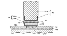
- FIG. 1 is a cross-sectional view of an electrostatic chuck 10 that is an embodiment of the joined body of the present invention cut along a central axis.
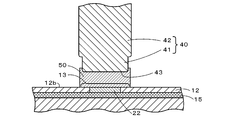
- FIG. 2 is an enlarged cross-sectional view of a joint portion between the ceramic substrate 12 and the power supply terminal 40 of FIG. 2 is shown upside down from FIG.
- the electrostatic electrode 14 and the heater electrode 15 are parallel to the wafer mounting surface 12a on the ceramic substrate 12 on which the wafer mounting surface 12a on which the wafer W can be mounted is formed. It is buried in.
- the ceramic substrate 12 is a disk-shaped member whose main component is a ceramic material such as alumina or aluminum nitride.
- the thickness of the ceramic substrate 12 is not particularly limited to this, but is, for example, 1 mm to 30 mm.
- the present invention is particularly effective for a thin structure in which no counterbore hole is provided.
- the electrostatic electrode 14 is a disk-shaped thin layer electrode having a smaller diameter than the ceramic substrate 12.
- the electrostatic electrode 14 may be a flat plate, or may be a mesh in which fine metal wires are knitted into a net shape to form a sheet.
- the electrostatic electrode 14 has a conductive tablet 16 connected to the center.
- the tablet 16 is exposed on the bottom surface of the counterbore 18 provided so as to reach the tablet 16 from the back surface 12 b of the ceramic substrate 12.
- a portion of the ceramic substrate 12 between the electrostatic electrode 14 and the wafer mounting surface 12a functions as a dielectric layer of the electrostatic chuck 60.
- a feed terminal 20 is inserted into the counterbore 18, and the feed terminal 20 is joined to the bottom surface (upper surface in FIG. 1) of the counterbore 18 and is electrically connected to the tablet 16.
- the power supply terminal 20 is a metal member, and examples of the material include Mo, Ti, and Kovar.
- the heater electrode 15 is formed so as to extend from one end near the center of the ceramic substrate 12 to the other end near the center after being stretched over the entire surface of the ceramic substrate 12 in the manner of one-stroke writing.
- the heater electrode 15 is connected to a conductive tablet 22 at one end and the other end.
- the diameter of the tablet 22 is, for example, 3 mm or less.
- Examples of the material of the tablet 22 include Mo, NbC, WC, Pt, and Nb.
- the tablet 22 is not exposed on the bottom surface of the countersink hole (concave portion) but directly exposed on the back surface 12 b of the ceramic substrate 12.
- the power supply terminal 40 is joined to the back surface 12b of the ceramic substrate 12, and the power supply terminal 40 and the tablet 22 are electrically connected.
- the power supply terminal 40 will be described in detail.
- the power supply terminal 40 is a substantially columnar member, and includes a small diameter portion 41 and a large diameter portion 42 having a diameter larger than that of the small diameter portion 41.
- the outer diameter of the large diameter portion 42 is, for example, 3 mm to 12 mm.
- An end surface (the lower surface in FIG. 2) on the small diameter portion 41 side of the power supply terminal 40 is a bonding surface 43.
- the bonding surface 43 is bonded to the bonding surface 13 of the ceramic substrate 12 via the bonding layer 50.
- the power supply terminal 40 is a metal member, and examples of the material include Mo, Ti, and Kovar. The bonding layer 50 will be described later.
- the bonding surface 13 is a part of the back surface 12 b of the ceramic substrate 12, and is a substantially circular region in contact with the lower surface of the bonding layer 50. Note that the tablet 22 is exposed in the bonding surface 13 of the back surface 12b, and the tablet 22 and the power supply terminal 40 are electrically connected to each other by bonding the tablet 22 and the power supply terminal 40 through the bonding layer 50. Yes.
- the thin film 114 is formed on the ceramic sintered body 111a, the tablet 16 is adhered to the center of the thin film 114, and the ceramic molded body (molded ceramic powder) 111b is formed thereon, and the first It is set as the intermediate body 127 (refer Fig.3 (a)).
- the thin film 114 is an electrode paste containing the raw material of the electrostatic electrode 14.
- the ceramic sintered body 111c is formed, and a bottomed hole is provided in a portion corresponding to one end and the other end of the heater electrode 15 in the ceramic sintered body 111c. Then, the tablet 22 is glued into each of the bottomed holes, and the pattern 115 is produced by screen printing or a doctor blade from above to form the second intermediate 128 (see FIG. 3B). The pattern 115 becomes the heater electrode 15 and is produced using the same raw material as the electrostatic electrode 14, for example.
- the second intermediate body 128 is disposed on the ceramic molded body 111b of the first intermediate body 127 so that the pattern 115 is in contact with the ceramic molded body 111b, and is integrated by uniaxial pressure molding to form the laminated body 129. (See FIG. 3C). Then, the laminated body 129 is made into the electrode built-in sintered body 130 by hot press firing (see FIG. 3D). Thereby, the ceramic sintered body 111a, the ceramic molded body 111b, and the ceramic sintered body 111c become one sintered body (ceramic base 12), the thin film 114 becomes the electrostatic electrode 14, and the pattern 115 becomes the heater electrode 15.
- the back surface side (the lower surface side in FIG. 3D) of the electrode built-in sintered body 130 is ground to expose the surface of the tablet 22 on the back surface 12b (see FIG. 3E).
- the surface side of the sintered body with built-in electrode 130 (the upper surface side in FIG. 3D) is also ground so that the surface roughness Ra of the wafer mounting surface 12a is 0.01 to 3 ⁇ m and the flatness is increased.
- the distance from the upper surface of the electrostatic electrode 14 to the wafer mounting surface 62a is preferably 0.2 to 1 mm.
- the countersink hole 18 is provided in the center of the back surface 12b of the electrode-containing sintered body 130 to expose the tablet 16 (see FIG. 3 (f)).
- the power supply terminal 20 is inserted into the countersink hole 18, and the power supply terminal 20 is joined to the bottom surface of the countersink hole 18 to make the tablet 16 and the power supply terminal 20 conductive.
- the power supply terminal 40 is joined to the back surface 12 b of the ceramic substrate 12, and the tablet 22 and the power supply terminal 40 are made conductive. Thereby, the electrostatic chuck 10 is completed (refer FIG.3 (g)).
- FIG. 1 is explanatory views of the bonding process between the ceramic substrate 12 and the power supply terminal 40.
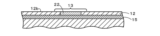
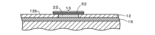
- a predetermined range which is a part of the back surface 12b of the ceramic substrate 12 is used as the bonding surface 13 (see FIG. 4), and the bonding surface 13 is covered with the substrate coating layer 52 (see FIG. 5).
- the joining surface 13 is determined so that the tablet 22 is exposed at the center in the joining surface 13.
- the wettability of the base coating layer 52 with respect to the brazing material 56 described later is higher than the wettability of the ceramic base 12 with respect to the brazing material 56.
- Examples of such a material for the substrate covering layer 52 include Ni and Au.
- the thickness of the base coating layer 52 is not particularly limited to this, but is, for example, 1 to 6 ⁇ m.
- the substrate covering layer 52 is formed by, for example, electroless plating or sputtering in a state where the back surface 12b except the bonding surface 13 is masked.
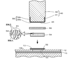
- a porous body 54, a brazing material 56, and a power supply terminal 40 are prepared, and these are placed on the bonding surface 13 (base coating layer 52) in this order as step (a) (FIG. 6). reference).
- the porous body 54 is made of a material having a smaller thermal expansion coefficient than the brazing material 56.
- the porous body 54 is a sintered body of ceramics such as alumina or aluminum nitride.
- the porous body 54 is obtained by, for example, molding and firing ceramic particles having an average particle diameter of 10 ⁇ m to 500 ⁇ m, preferably 20 ⁇ m to 100 ⁇ m.
- the porous body 54 is preferably a sintered body made of the same ceramic material as the ceramic substrate 12.
- the porous body 54 preferably has a porosity of 30% to 50%.
- the porous body 54 preferably has a dry air flow rate of 50 ml / (cm 2 ⁇ min) to 150 ml / (cm 2 ⁇ min).
- the porosity of the porous body 54 is a value measured by the Archimedes method.
- the dry air flow rate is a value measured based on JIS-Z8762 (1988) and JIS-B8330 (1981). Specifically, in a room that is controlled at room temperature (20 ° C ⁇ 3 ° C), an orifice plate and an air tank are arranged in the air flow path from the blower that blows air to the porous body 54, and the blower blows air.
- the differential pressure across the orifice plate when a specified amount of air pressure is applied to the air tank is measured, and the value obtained by converting the measured differential pressure into the ventilation rate is defined as the dry ventilation rate.
- the surface of the internal pores is covered with the pore coating layer 55 (see the enlarged portion in FIG. 6).
- the pore covering layer 55 covers at least a part of the surface of the open pores among the pore surfaces of the porous body 54.
- the pore covering layer 55 does not need to cover the surface of the closed pores.
- the pore covering layer 55 may also cover the outer surface of the porous body 54 (not the surface of the pores, but the upper surface, the lower surface, the side surface, etc. of the porous body 54).
- the “porosity” and “dry air flow rate” of the porous body 54 described above are values before the pore covering layer 55 is formed.
- the “porosity” of the porous body 54 is the porosity of the porous body when it is assumed that there is no pore covering layer 55, and more specifically, the porosity covering layer 55 within the porous body 54. It is set as the porosity when the portion where the air is present is regarded as a pore (space).
- the wettability of the pore covering layer 55 with respect to the brazing material 56 is higher than the wettability of the porous body 54 with respect to the brazing material 56.
- Examples of the material for the pore covering layer 55 include Ni and Au.
- the thickness of the pore covering layer 55 is not particularly limited to this.
- the thickness is 1 ⁇ m to 6 ⁇ m, and may be 1 ⁇ m to 3 ⁇ m.
- the thickness of the pore covering layer 55 is a value measured by cross-sectional observation with an electron microscope (SEM).
- the pore covering layer 55 can be formed by electroless plating, for example.
- the brazing material 56 can easily penetrate into the pores of the porous body 54 by increasing the amount of the pore covering layer 55 formed on the pore surfaces in the porous body 54 (the area covering the surface of the pores). . The more the brazing material 56 penetrates into the pores of the porous body 54, the higher the conductivity of the bonded layer 50 after bonding can be.
- the brazing material 56 is made of a metal having, for example, aluminum as a main component and a thermal expansion coefficient larger than that of the ceramic substrate 12.
- the brazing material 56 has a plate shape (disc shape).
- the diameter of the brazing material 56 (the length in the left-right direction in FIG. 6) may be larger than the diameters of the brazing material 56 and the joining surface 43 as shown in FIG.
- the power supply terminal 40 has the shape described above. In the power supply terminal 40, the end portion (the lower end portion in FIG. 6) on the joint surface 43 side is previously covered with the terminal covering layer 58.
- the terminal coating layer 58 is formed in a bottomed cylindrical shape, and includes a bottom coating layer 58a and a side coating layer 58b.
- the bottom cover layer 58 a covers the bonding surface 43 that is the bottom surface of the small diameter portion 41 of the power supply terminal 40.
- the side portion covering layer 58b covers the side surface of the power supply terminal 40 (the outer peripheral surface of the small diameter portion 41).
- the bottom coating layer 58a and the side coating layer 58b are continuous at the corners of the joint surface 43 and the side surface of the power supply terminal 40, and both are integrally formed.
- the wettability of the terminal coating layer 58 with respect to the brazing material 56 is higher than the wettability of the power supply terminal 40 with respect to the brazing material 56.
- Examples of the material of the terminal coating layer 58 include Ni and Au.
- the thickness of the terminal coating layer 58 is not particularly limited, but is, for example, 1 to 6 ⁇ m.
- the terminal coating layer 58 is formed by electroless plating, electrolytic plating, sputtering, or the like in a state where a portion of the power supply terminal 40 where the side coating layer 58b is not formed, such as the outer peripheral surface of the large diameter portion 42, is masked.
- the bonding surface 13 of the ceramic base 12 and the bonding surface 43 of the power supply terminal 40 face each other (see FIG. 7). ).
- the porous body 54 is in contact with the base coating layer 52 and the brazing material 56.
- the terminal covering layer 58 is in contact with the brazing material 56.
- step (b) is subsequently performed.
- the brazing material 56 is melted, and the brazing material 56 is permeated into the pores (open pores) of the porous body 54.
- the bonding layer 50 including the brazing material 56 and the porous body 54 is formed, and the bonding surface 13 of the ceramic base 12 and the bonding surface 43 of the power supply terminal 40 are bonded via the bonding layer 50.
- the solder material 56 penetrated into the open pores of the porous body 54 and adhered to the outer surface of the porous body 54 (the upper surface, the lower surface, the side surface, etc. of the porous body 54, not the surface of the pores).
- the brazing material 56 By the brazing material 56, the power supply terminal 40 (joint surface 43) and the tablet 22 are electrically connected.
- the substrate covering layer 52, the pore covering layer 55, and the terminal covering layer 58 may also be melted and mixed with the brazing material 56 to become a part of the bonding layer 50.
- a joined body electrostatic chuck 10 in which the power supply terminal 40 is joined to the ceramic base 12 is manufactured (see FIG. 2).
- the porous body 54 included in the bonding layer 50 thus manufactured is in a state in which the pores are filled with a metal such as the brazing material 56.
- the porosity of the porous body 54 (also referred to as virtual porosity) is preferably 30% to 50%.
- the virtual porosity of the bonding layer 50 can be obtained by capturing a cross-sectional image by capturing a cross-section of the bonding layer 50 with an electron microscope (SEM) and performing image processing on the cross-sectional image. it can. Specifically, for example, by comparing information such as the luminance of each pixel in the cross-sectional image with a predetermined threshold value and binarizing, each pixel is a portion other than the porous body 54 and the porous body 54 (porous And the ratio of the pixels other than the porous body 54 in all the pixels in the cross-sectional image can be obtained as the virtual porosity.
- the virtual porosity is substantially the same value as the “porosity” of the porous body 54 described above (porosity before coating of the pore coating layer 55).
- the temperature at which the brazing material 56 is melted in the step (b) is, for example, 10 ° C. to 150 ° C. higher than the melting point of the brazing material 56, and preferably 100 ° C. to 150 ° C. higher.
- the holding time of this temperature is, for example, 5 minutes to 90 minutes, preferably 10 minutes to 30 minutes.
- the atmosphere during the bonding is preferably an atmosphere with a high degree of vacuum, for example, 1 ⁇ 10 ⁇ 4 Torr or less, and more preferably 2 ⁇ 10 ⁇ 5 Torr or less. Bonding may be performed in a state where the power supply terminal 40 is pressed toward the ceramic substrate 12.
- the porous body 54, the brazing material 56, and the power supply terminal 40 are inserted into the countersink hole 18, and the above-described steps (a) to (a) to FIG. You may carry out similarly to a process (b).
- powder made of the same material as the porous body 54 is spread on the bottom surface of the counterbore hole 18, and then the brazing material 56 and the power supply terminal 40 are inserted into the counterbore hole 18, The power supply terminal 20 and the bottom surface of the counterbore 18 may be joined by melting the brazing material 56 in the same manner as in the step (b) described above.
- a usage example of the electrostatic chuck 10 of the present embodiment will be briefly described below.
- the wafer W is mounted on the wafer mounting surface 12a of the electrostatic chuck 10, and an electrostatic force is generated by applying a DC high voltage to the electrostatic electrode 14 through the power supply terminal 20 of the electrostatic electrode 14. Thereby, the wafer W is attracted to the wafer mounting surface 12a.
- a heater power supply is connected to the two power supply terminals 40, 40 of the heater electrode 15, and the power supplied is controlled to adjust the wafer W to a desired temperature. In this state, plasma CVD film formation or plasma etching is performed on the wafer W.
- a high-frequency voltage is applied to the electrostatic electrode 14 through a power supply terminal 20 in a vacuum chamber (not shown) and embedded in the electrostatic chuck 10 and a counter horizontal electrode (not shown) installed above the vacuum chamber.
- Plasma is generated between the parallel plate electrodes composed of the electrostatic electrodes 14, and CVD is performed on the wafer W or etching is performed using the plasma.
- the ceramic substrate 12 of the present embodiment corresponds to the first member of the present invention
- the power supply terminal 40 corresponds to the second member
- the brazing material 56 corresponds to the brazing material
- the porous body 54 corresponds to the porous body.
- the bonding layer 50 corresponds to the bonding layer.
- the brazing material 56, the porous body 54 and the power supply are supplied in the step (a).
- the terminal 40 is disposed on the bonding surface 13 of the ceramic substrate 12.
- the brazing material 56 is melted and permeated into the pores of the porous body 54 to form a joining layer 50 including the brazing material 56 and the porous body 54, and the ceramic substrate 12 and the power supply terminal 40 are joined.
- the bonding layer 50 is formed using the brazing material 56 and the porous body 54, the ceramic base 12 does not have a rising portion from the bonding surface 13 (the ceramic base 12 has the bonding surface 13 as the bottom surface).
- the ceramic substrate 12 and the power supply terminal 40 can be joined even in the case where there is no recess to be provided). That is, for example, when powder of the same material is used instead of the porous body 54, the powder spreads when the flat portion having no recess in the ceramic substrate 12 is the bonding surface 13. Such a thing does not arise by using. Further, since the bonding layer 50 is formed using the brazing material 56 having a larger thermal expansion coefficient than that of the first member and the porous body 54 made of a material having a smaller thermal expansion coefficient than that of the brazing material 56, for example, only the brazing material 56 is used. As compared with the case where the bonding layer 50 is formed, the occurrence of cracks in the ceramic substrate 12 when the temperature of the electrostatic chuck 10 changes can be further suppressed.
- the following effects can be obtained by setting the porosity of the porous body 54 to 30% to 50%. That is, by setting the porosity of the porous body 54 to the lower limit value or more, the brazing material 56 can penetrate more into the porous body 54, and the bonding strength is improved. Further, by setting the porosity of the porous body 54 to the upper limit value or less, the porous body 54 having a smaller thermal expansion coefficient than the brazing material 56 is present, so that the electrostatic chuck 10 changes in temperature. The occurrence of cracks in the ceramic substrate 12 at this time can be further suppressed.
- the porous body 54 is made of a porous sintered body made of the same ceramic material as the ceramic base 12, the ceramic base 12 and the porous body 54 have substantially the same thermal expansion coefficient. The occurrence of cracks in the ceramic substrate 12 when the temperature changes can be further suppressed.
- step (a) the porous body 54 is covered with a pore coating layer 55 made of a material having higher wettability with respect to the brazing material 56 on the surface of the inner pores than the porous body 54.
- the brazing material 56 can easily penetrate into the pores of the porous body 54, so that the bonding strength of the electrostatic chuck 10 can be improved.
- both of the bonding surface 13 of the ceramic substrate 12 and the bonding surface 43 of the power supply terminal 40 are made of a material having higher wettability with respect to the brazing material 56 and the terminal coating layer 58. Respectively. Therefore, the coated bonding surface 13 and the bonding surface 43 are easily wetted by the brazing material 56, and the bonding strength of the electrostatic chuck 10 can be improved.
- the ceramic substrate 12 does not have a rising portion from the bonding surface 13, it is highly significant to apply the present invention.
- the ceramic base 12 needs to have an extra thickness corresponding to the height of the countersink hole. 12 is difficult to thin.
- a semiconductor susceptor such as the electrostatic chuck 10 is required to be relatively thin, for example, the thickness of the ceramic substrate 12 is 1 mm.
- the ceramic substrate 12 and the power supply terminal 40 can be bonded without using the bonding surface 13 as the bottom surface of the countersink hole, so that the ceramic substrate 12 can be easily thinned.
- the substrate covering layer 52, the pore covering layer 55, and the terminal covering layer 58 are formed, but one or more of them may be omitted. If the wettability of one or more of the bonding surface 13, the bonding surface 43, and the porous body 54 with respect to the brazing material 56 is sufficiently high, even if the corresponding coating layer is omitted, the ceramic substrate 12 and the feeding terminal 40 formed by the bonding layer 50 The joining force is sufficient. Further, only the bottom covering layer 58a of the terminal covering layer 58 may be formed, and the side covering layer 58b may be omitted.
- the power supply terminal 40 includes the small diameter portion 41 and the large diameter portion 42, but is not limited thereto.
- the power supply terminal 40 may be a cylindrical member having the same diameter from the upper end to the lower end. That is, the small diameter portion 41 and the large diameter portion 42 in the power supply terminal 40 may have the same diameter.
- the porous body 54 is disposed so as to sandwich the brazing material 56 between the joint surface 13 and the joint surface 43 in the step (a), but is not limited thereto.
- the brazing material 56 may be disposed so as to be inserted into an insertion hole formed in the power supply terminal 40.
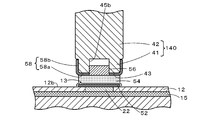
- FIG. 8 is an enlarged cross-sectional view of a joint portion between the ceramic substrate 12 and the power supply terminal 140 of the modification.
- the power supply terminal 140 has an insertion hole 45 b formed in the small diameter portion 41.
- the insertion hole 45b opens on the surface on the side of the joint surface 43 (the lower surface in FIG. 8). Therefore, in the power supply terminal 140, the joint surface 43 has a ring shape.
- step (a) When joining such a power supply terminal 140 to the joint surface 13, in step (a), as shown in FIG. 8, with the brazing material 56 inserted into the insertion hole 45 b of the power supply terminal 40, the power supply terminal 40 (and A brazing material 56) is placed on the porous body 54. Thereafter, in the step (b), the brazing material 56 is melted to form the bonding layer 50 including the porous body 54 and the brazing material 56, as in the above-described embodiment, and the ceramic base 12 and the power supply terminal 240. And can be joined.
- the power supply terminal 20 is joined to the bottom surface of the counterbore 18 in the ceramic substrate 12, but is not limited thereto.
- the surface of the tablet 16 may be exposed to the back surface 12b of the ceramic substrate 12 without forming the counterbore 18.
- the back surface 12b including the exposed surface of the tablet 16 and the power supply terminal 20 may be bonded via the bonding layer 50 in the same manner as the bonding of the ceramic base 12 and the power supply terminal 40 of the above-described embodiment.
- Example 1 As Example 1, a joined body of the ceramic substrate 12 and the power supply terminal 40 was produced in the same manner as in the manufacturing method described with reference to FIGS. Specifically, first, an alumina powder having a purity of 99.5% is fired to a density of 99.5% or more and ground to produce a disc-shaped alumina sintered body having an outer diameter of 300 mm and a thickness of 5 mm. A substrate 12 was obtained. In Example 1, a tablet 22 made of Mo was embedded in alumina powder, and the fired ceramic substrate 12 was ground to expose the surface of the tablet 22.
- a region having a diameter of 4 mm (including a region having a diameter of 2.0 mm, which is the surface of the tablet 22) of the ceramic substrate 12 is used as a bonding surface 13, and other than the bonding surface 13 is masked to have a purity of 99% and a thickness of about
- An electroless Ni plating having a thickness of 1 ⁇ m was formed to form a base coating layer 52 having a diameter of 4 mm that covers the bonding surface 13.
- a brazing material 56, a power supply terminal 40, and a porous body 54 (made of alumina, having a porosity of 38% and a dry air flow rate of 110 ml / (cm 2 ⁇ min)) were prepared.
- the porous body 54 has a pore covering layer 55 made of electroless Ni plating having a thickness of 1 to 2 ⁇ m on the surface of the open pores in advance.
- the pore covering layer 55 was formed as follows: First, the following treatment was performed as a pretreatment (nucleation treatment): a tin chloride solution was injected into the porous body 54.
- the tin chloride solution was sucked off, rinsed with pure water, moisture was removed by nitrogen blowing, and then the Pt solution was injected into the porous body 54 and held for 2 minutes. Absorb tin solution, rinse with pure water, and remove moisture with nitrogen blow.
- This pre-treatment was performed twice in total, and then the following treatment was performed as a plating process: the porous body 54 was placed on a hot plate, and the surface temperature reached 80 to 85 ° C. Then, an electroless Ni plating solution was injected into the porous body 54. After replacing the electroless Ni plating solution as appropriate, the electroless Ni plating solution was discharged and the porous body 54 was washed with pure water.
- the pore covering layer 55 was formed by the above processing.
- the brazing material 56 was made of an Al—Si—Mg based alloy (JIS BA 4004), and had a disk shape with a diameter of 5 mm and a thickness of 0.12 mm.
- the power supply terminal 40 is made of Mo, the outer diameter of the small diameter portion 41 is 4 mm, the axial length of the small diameter portion 41 is 1 mm, the outer diameter of the large diameter portion 42 is 5 mm, and the axial length of the large diameter portion 42 is 5 mm. It was. Further, a terminal coating layer 58 composed of a bottom coating layer 58 a and a side coating layer 58 b was formed on the small diameter portion 41 of the power supply terminal 40.
- the terminal coating layer 58 was formed as follows.
- ultrasonic cleaning using acetone for the power supply terminal 40 was performed for 5 minutes, then ultrasonic cleaning using pure water was performed for 10 minutes, and then nitrogen blowing was performed at 120 ° C. for 10 minutes to dry and remove the moisture on the surface.
- a terminal coating layer 58 made of electroless Ni plating having a thickness of 1 ⁇ m was formed.
- the side portion coating layer 58b covers the entire side surface of the small diameter portion 41.
- the porous body 54, the brazing material 56, and the power supply terminal 40 were placed on the bonding surface 13 (base coating layer 52) in this order.
- the ceramic substrate 12, the power supply terminal 40, the brazing material 56, and the porous body 54 arranged in the step (a) are put into a firing furnace and heated to form the bonding layer 50.
- the ceramic substrate 12 and the power supply terminal 40 were joined.
- the heating conditions were a temperature of 700 ° C. ⁇ 20 ° C., a holding time of 10 minutes, and a degree of vacuum of 5 ⁇ 10 ⁇ 5 Torr or less.
- the power supply terminal 40 was pressed toward the ceramic substrate 12 with a weight of 125 gf.
- the joined body was taken out from the firing furnace.
- the bonded body of Example 1 was produced by the above.
- the virtual porosity of the bonding layer 50 (porous body 54) of the bonded body was 43%.
- the virtual porosity is calculated by obtaining a SEM image of the cross section of the bonding layer 50 using a scanning electron microscope (JEOL JSM-5900), and using the image processing software HALCON 11.0 (HALCON is a product of MVTec Software GmbH). This was performed by binarizing with the luminance of each pixel using a registered trademark.
- Comparative Example 1 A joined body was produced in the same manner as in Example 1 except that the porous body 54 was not used and the ceramic substrate 12 and the power feeding terminal 40 were joined with the brazing material 56 to obtain Comparative Example 1.
- the bonding strength of the bonded body of Example 1 was measured by applying a force in the direction in which the ceramic substrate 12 and the power supply terminal 40 were separated from each other, the bonding strength was 40 kgf, which was a sufficiently practical value for the electrostatic chuck 10. .
- the bonding strength was measured using a tensile strength tester (manufactured by Shimadzu Corporation, Autograph).
- Example 1 and Comparative Example 1 were heated at a rate of 5 ° C./second from room temperature to 100 ° C., and then returned to room temperature by natural cooling. This process was repeated 1000 times. Then, the presence or absence of the crack of a joined body was confirmed. In the joined body of Example 1, no cracks were observed, but in the joined body of Comparative Example 1, cracks occurred in the ceramic substrate 12.
- Example 2 An attempt was made to produce a joined body in the same manner as in Example 1 except that powder made of ceramic particles of the same material as the porous body 54 was used instead of the porous body 54. However, the powder spreads on the surface of the ceramic substrate 12, and the ceramic substrate 12 and the power supply terminal 40 were not joined even when overheated in a firing furnace.
- Examples 2 to 11 Except that the porous body 54 having a porosity shown in Table 1 was used, joined bodies were produced in the same manner as in Example 1 and designated as Examples 2 to 11. With respect to Examples 2 to 11, as initial characteristics, the breaking strength (bonding strength) and the presence / absence of cracks of the initial bonded body produced were measured. Moreover, the breaking strength of the joined body after the thermal cycle test and the presence or absence of cracks were also measured. In the heat cycle test, the joined bodies of Examples 2 to 11 were heated at a rate of 5 ° C./second from room temperature to 100 ° C. using an external heater, and then returned to room temperature by natural cooling. This process was repeated 1000 times. In each example, a plurality of joined bodies were prepared, and the measurement of initial characteristics and the measurement after the thermal cycle test were performed on separate joined bodies.
- Table 1 summarizes the porosity of the porous body 54 used in Examples 2 to 11, the breaking strength and the presence or absence of cracks at the beginning of the production, the breaking strength and the presence or absence of cracks after the thermal cycle test. Show.
- the crack index is as follows: A: no cracks are observed, B: cracks are observed, but the degree is minor and does not affect the bonding characteristics, C: cracks that affect the bonding characteristics are observed, Means.
- Examples 4 to 9 using the porous body 54 having a porosity of 30% to 50% are the same as Examples 2 and 3 in which the porosity is below 30%.
- both the initial and post-thermal cycle breaking strengths were high.
- the breaking strength after the initial stage and after the thermal cycle was 30 kgf or more, which is a value that can be sufficiently used as the electrostatic chuck 10.
- the initial bonding strength was 30 kg or more, and no cracks were generated so as to affect the bonding characteristics. Cracks occurred in the substrate 12.
- no crack was observed both in the initial stage and after the thermal cycle.
- the porosity of the porous body 54 is 30% or more, so that the brazing material 56 can penetrate more into the porous body 54 and the bonding strength is improved. It is done. Further, by setting the porosity of the porous body 54 to 50% or less, the porous body 54 having a smaller thermal expansion coefficient than that of the brazing material 56 is present, and therefore, when the temperature of the joined body changes. It is considered that the occurrence of cracks in the film can be further suppressed.
- the present invention can be used for a semiconductor manufacturing apparatus, for example, an electrostatic chuck for supporting a wafer.
- electrostatic chuck 12 ceramic substrate, 12a wafer mounting surface, 12b back surface, 13 bonding surface, 14 electrostatic electrode, 15 heater electrode, 16 tablet, 18 countersink hole, 20 power supply terminal, 22 tablet, 40 power supply terminal, 41 small diameter portion, 42 large diameter portion, 43 bonding surface, 45b insertion hole, 50 bonding layer, 52 base coating layer, 54 porous body, 55 pore coating layer, 56 brazing material, 58 terminal coating layer, 58a bottom coating layer, 58b side covering layer, 111a ceramic sintered body, 111b ceramic molded body, 111c ceramic sintered body, 114 thin film, 115 pattern, 127 first intermediate, 128 second intermediate, 129 laminate, 130 built-in electrode sintering Body, 140 power supply terminal.
Landscapes
- Chemical & Material Sciences (AREA)
- Engineering & Computer Science (AREA)
- Ceramic Engineering (AREA)
- Materials Engineering (AREA)
- Structural Engineering (AREA)
- Organic Chemistry (AREA)
- Manufacturing & Machinery (AREA)
- Inorganic Chemistry (AREA)
- Container, Conveyance, Adherence, Positioning, Of Wafer (AREA)
- Ceramic Products (AREA)
Abstract
Description
セラミックスからなる第1部材の接合面と金属からなる第2部材の接合面とを接合層を介して接合した接合体の製造方法であって、
(a)前記第1部材よりも熱膨張係数の大きい金属からなるロウ材と、該ロウ材よりも熱膨張係数の小さい多孔質体と、前記第2部材とを、該第1部材の接合面上に配置する工程と、
(b)前記ロウ材を溶融させ、該ロウ材を前記多孔質体の気孔内に浸透させて該ロウ材と該多孔質体とを含む接合層を形成して、該接合層を介して前記第1部材の接合面と前記第2部材の接合面とを接合する工程と、
を含むものである。
セラミックスからなる第1部材と、
金属からなる第2部材と、
気孔内に前記第1部材よりも熱膨張係数の大きい金属が充填され該金属よりも熱膨張係数の小さい材料からなり該金属がないと仮定した場合の気孔率が30%~50%である多孔質体を有し、前記第1部材と前記第2部材とを接合する接合層と、
を備えたものである。
実施例1として、上述した図4~図7で説明した製造方法と同様にして、セラミックス基体12と給電端子40との接合体を作製した。具体的には、まず、純度99.5%のアルミナ粉末を焼成後密度99.5%以上とし、研削して、外径300mm、厚さ5mmの円盤状のアルミナ焼結体を作製し、セラミックス基体12とした。なお、実施例1では、アルミナ粉末にMo製のタブレット22を埋設しておき、焼成後のセラミックス基体12を研削してタブレット22の表面を露出させた。そして、このセラミックス基体12のうち直径4mmの領域(タブレット22の表面である直径2.0mmの領域を含む)を接合面13として、この接合面13以外をマスキングして純度99%,厚さ約1μmの無電解Niメッキを形成し、接合面13上を被覆する直径4mmの基体被覆層52とした。
多孔質体54を用いず、ロウ材56でセラミックス基体12と給電端子40とを接合した点以外は、実施例1と同様にして接合体を作製し、比較例1とした。
多孔質体54の代わりに多孔質体54と同じ材質のセラミックス粒子からなる粉末を用いた点以外は、実施例1と同様にして接合体を作製しようとした。しかし、粉末がセラミックス基体12の表面に広がってしまい、焼成炉で過熱してもセラミックス基体12と給電端子40とが接合されなかった。
多孔質体54の気孔率が表1に示す値のものを使用した点以外は実施例1と同様にして接合体を作製し、実施例2~11とした。実施例2~11について、初期特性として、作製した当初の接合体の破断強度(接合強度)とクラックの有無を測定した。また、熱サイクル試験後の接合体の破断強度とクラックの有無も測定した。熱サイクル試験は、外部加熱ヒーターを用いて、実施例2~11の接合体を室温から100℃になるまで5℃/秒の速度で昇温し、その後自然放冷により、室温まで戻した。この工程を1000回繰り返した。なお、各実施例においてそれぞれ複数の接合体を作製し、初期特性の測定と熱サイクル試験後の測定とは別々の接合体について行った。

Claims (7)
- セラミックスからなる第1部材の接合面と金属からなる第2部材の接合面とを接合層を介して接合した接合体の製造方法であって、
(a)前記第1部材よりも熱膨張係数の大きい金属からなるロウ材と、該ロウ材よりも熱膨張係数の小さい多孔質体と、前記第2部材とを、該第1部材の接合面上に配置する工程と、
(b)前記ロウ材を溶融させ、該ロウ材を前記多孔質体の気孔内に浸透させて該ロウ材と該多孔質体とを含む接合層を形成して、該接合層を介して前記第1部材の接合面と前記第2部材の接合面とを接合する工程と、
を含む接合体の製造方法。 - 前記多孔質体は、気孔率が30%~50%である、
請求項1に記載の接合体の製造方法。 - 前記多孔質体は、前記第1部材と同じセラミックス材料からなる多孔質焼結体である、
請求項1又は2に記載の接合体の製造方法。 - 前記工程(a)において、前記多孔質体は、内部の気孔の表面が自身と比べて前記ロウ材に対する濡れ性の高い材料で被覆されている、
請求項1~3のいずれか1項に記載の接合体の製造方法。 - 前記工程(a)において、前記第1部材の接合面と、前記第2部材の接合面と、の少なくとも一方が、自身と比べて前記ロウ材に対する濡れ性の高い材料で被覆されている、
請求項1~4のいずれか1項に記載の接合体の製造方法。 - 前記第1部材は、前記接合面からの立ち上がり部を有さない、
請求項1~5のいずれか1項に記載の接合体の製造方法。 - セラミックスからなる第1部材と、
金属からなる第2部材と、
気孔内に前記第1部材よりも熱膨張係数の大きい金属が充填され該金属よりも熱膨張係数の小さい材料からなり該金属がないと仮定した場合の気孔率が30%~50%である多孔質体を有し、前記第1部材と前記第2部材とを接合する接合層と、
を備えた接合体。
Priority Applications (4)
| Application Number | Priority Date | Filing Date | Title |
|---|---|---|---|
| JP2016506552A JP6921532B2 (ja) | 2014-03-07 | 2015-03-05 | 接合体の製造方法及び接合体 |
| CN201580011169.XA CN106061924B (zh) | 2014-03-07 | 2015-03-05 | 接合体的制造方法以及接合体 |
| KR1020167023900A KR102399753B1 (ko) | 2014-03-07 | 2015-03-05 | 접합체의 제조 방법 및 접합체 |
| US15/244,397 US10332771B2 (en) | 2014-03-07 | 2016-08-23 | Joined body manufacturing method and joined body |
Applications Claiming Priority (2)
| Application Number | Priority Date | Filing Date | Title |
|---|---|---|---|
| JP2014044944 | 2014-03-07 | ||
| JP2014-044944 | 2014-03-07 |
Related Child Applications (1)
| Application Number | Title | Priority Date | Filing Date |
|---|---|---|---|
| US15/244,397 Continuation US10332771B2 (en) | 2014-03-07 | 2016-08-23 | Joined body manufacturing method and joined body |
Publications (1)
| Publication Number | Publication Date |
|---|---|
| WO2015133576A1 true WO2015133576A1 (ja) | 2015-09-11 |
Family
ID=54055376
Family Applications (1)
| Application Number | Title | Priority Date | Filing Date |
|---|---|---|---|
| PCT/JP2015/056525 Ceased WO2015133576A1 (ja) | 2014-03-07 | 2015-03-05 | 接合体の製造方法及び接合体 |
Country Status (5)
| Country | Link |
|---|---|
| US (1) | US10332771B2 (ja) |
| JP (1) | JP6921532B2 (ja) |
| KR (1) | KR102399753B1 (ja) |
| CN (1) | CN106061924B (ja) |
| WO (1) | WO2015133576A1 (ja) |
Cited By (5)
| Publication number | Priority date | Publication date | Assignee | Title |
|---|---|---|---|---|
| WO2017115599A1 (ja) * | 2015-12-28 | 2017-07-06 | 日本特殊陶業株式会社 | セラミックス部材 |
| JP2019208006A (ja) * | 2018-05-29 | 2019-12-05 | 日本特殊陶業株式会社 | 電極埋設部材の製造方法 |
| JP2020075834A (ja) * | 2018-11-08 | 2020-05-21 | 日本特殊陶業株式会社 | 接合体 |
| JP2021170567A (ja) * | 2020-04-14 | 2021-10-28 | 日本特殊陶業株式会社 | 保持装置及び保持装置の製造方法 |
| JP7606635B1 (ja) * | 2023-07-06 | 2024-12-25 | 日本碍子株式会社 | 半導体製造装置用部材 |
Families Citing this family (9)
| Publication number | Priority date | Publication date | Assignee | Title |
|---|---|---|---|---|
| MY194354A (en) * | 2016-12-21 | 2022-11-29 | Furukawa Electric Co Ltd | Joining film and tape for wafer processing |
| KR102259995B1 (ko) * | 2017-10-30 | 2021-06-02 | 니뽄 도쿠슈 도교 가부시키가이샤 | 전극 매설 부재 |
| JP6994644B2 (ja) * | 2017-12-01 | 2022-01-14 | パナソニックIpマネジメント株式会社 | 接合体と接合方法および接合材料 |
| CN109721379B (zh) * | 2019-03-14 | 2021-11-02 | 大连海事大学 | 一种用AlON粉体作为原料连接AlON陶瓷的方法 |
| TWI828988B (zh) * | 2020-06-26 | 2024-01-11 | 日商日本特殊陶業股份有限公司 | 接合體及靜電夾頭 |
| JP7438070B2 (ja) * | 2020-09-11 | 2024-02-26 | 新光電気工業株式会社 | 静電チャック、基板固定装置及び基板固定装置の製造方法 |
| JP7761519B2 (ja) * | 2022-03-31 | 2025-10-28 | 日本碍子株式会社 | 接合構造体 |
| JP2024128820A (ja) * | 2023-03-10 | 2024-09-24 | 住友電気工業株式会社 | ウエハ加熱装置 |
| CN116354739B (zh) * | 2023-03-13 | 2024-02-02 | 中国科学院宁波材料技术与工程研究所 | 一种陶瓷连接件及其制备方法与应用 |
Citations (6)
| Publication number | Priority date | Publication date | Assignee | Title |
|---|---|---|---|---|
| JPS60223655A (ja) * | 1984-04-23 | 1985-11-08 | Daido Steel Co Ltd | セラミクス−金属複合体の製造方法 |
| JPH06329481A (ja) * | 1993-05-20 | 1994-11-29 | Noritake Co Ltd | セラミックス−金属複合体およびその製造方法 |
| JPH08253373A (ja) * | 1995-03-15 | 1996-10-01 | Toshiba Corp | 真空気密容器用封着材、真空気密容器、およびセラミックス−金属接合体の製造方法 |
| JP2011091417A (ja) * | 2004-04-05 | 2011-05-06 | Mitsubishi Materials Corp | Al/AlN接合体、パワーモジュール用基板及びパワーモジュール並びにAl/AlN接合体の製造方法 |
| JP2012091975A (ja) * | 2010-10-28 | 2012-05-17 | Mitsubishi Materials Corp | セラミックス材と金属材との接合体の製造方法 |
| JP2013193935A (ja) * | 2012-03-21 | 2013-09-30 | Ngk Insulators Ltd | セラミックス部材と金属部材との接合体及びその製法 |
Family Cites Families (10)
| Publication number | Priority date | Publication date | Assignee | Title |
|---|---|---|---|---|
| EP0097944B1 (en) * | 1982-06-29 | 1988-06-01 | Kabushiki Kaisha Toshiba | Method for directly bonding ceramic and metal members and laminated body of the same |
| WO2004074210A1 (ja) * | 1992-07-03 | 2004-09-02 | Masanori Hirano | セラミックス-金属複合体およびその製造方法 |
| US5675181A (en) * | 1995-01-19 | 1997-10-07 | Fuji Electric Co., Ltd. | Zirconia-added alumina substrate with direct bonding of copper |
| JP3491414B2 (ja) * | 1995-11-08 | 2004-01-26 | 三菱電機株式会社 | 回路基板 |
| JP3315919B2 (ja) * | 1998-02-18 | 2002-08-19 | 日本碍子株式会社 | 2種類以上の異種部材よりなる複合部材を製造する方法 |
| JP3792440B2 (ja) * | 1999-06-25 | 2006-07-05 | 日本碍子株式会社 | 異種部材の接合方法、および同接合方法により接合された複合部材 |
| JP2001220252A (ja) * | 2000-02-01 | 2001-08-14 | Nok Corp | 接合体およびその製造方法 |
| JP3989254B2 (ja) * | 2002-01-25 | 2007-10-10 | 日本碍子株式会社 | 異種材料接合体及びその製造方法 |
| JP4879929B2 (ja) * | 2008-03-26 | 2012-02-22 | 日本碍子株式会社 | 静電チャック及びその製造方法 |
| JP2011139000A (ja) * | 2010-01-04 | 2011-07-14 | Denki Kagaku Kogyo Kk | パワーモジュール構造体及びその製造方法 |
-
2015
- 2015-03-05 WO PCT/JP2015/056525 patent/WO2015133576A1/ja not_active Ceased
- 2015-03-05 JP JP2016506552A patent/JP6921532B2/ja active Active
- 2015-03-05 KR KR1020167023900A patent/KR102399753B1/ko active Active
- 2015-03-05 CN CN201580011169.XA patent/CN106061924B/zh active Active
-
2016
- 2016-08-23 US US15/244,397 patent/US10332771B2/en active Active
Patent Citations (6)
| Publication number | Priority date | Publication date | Assignee | Title |
|---|---|---|---|---|
| JPS60223655A (ja) * | 1984-04-23 | 1985-11-08 | Daido Steel Co Ltd | セラミクス−金属複合体の製造方法 |
| JPH06329481A (ja) * | 1993-05-20 | 1994-11-29 | Noritake Co Ltd | セラミックス−金属複合体およびその製造方法 |
| JPH08253373A (ja) * | 1995-03-15 | 1996-10-01 | Toshiba Corp | 真空気密容器用封着材、真空気密容器、およびセラミックス−金属接合体の製造方法 |
| JP2011091417A (ja) * | 2004-04-05 | 2011-05-06 | Mitsubishi Materials Corp | Al/AlN接合体、パワーモジュール用基板及びパワーモジュール並びにAl/AlN接合体の製造方法 |
| JP2012091975A (ja) * | 2010-10-28 | 2012-05-17 | Mitsubishi Materials Corp | セラミックス材と金属材との接合体の製造方法 |
| JP2013193935A (ja) * | 2012-03-21 | 2013-09-30 | Ngk Insulators Ltd | セラミックス部材と金属部材との接合体及びその製法 |
Cited By (12)
| Publication number | Priority date | Publication date | Assignee | Title |
|---|---|---|---|---|
| WO2017115599A1 (ja) * | 2015-12-28 | 2017-07-06 | 日本特殊陶業株式会社 | セラミックス部材 |
| JP2017119593A (ja) * | 2015-12-28 | 2017-07-06 | 日本特殊陶業株式会社 | セラミックス部材 |
| US10880955B2 (en) | 2015-12-28 | 2020-12-29 | Ngk Spark Plug Co., Ltd. | Ceramic member |
| JP2019208006A (ja) * | 2018-05-29 | 2019-12-05 | 日本特殊陶業株式会社 | 電極埋設部材の製造方法 |
| JP7280059B2 (ja) | 2018-05-29 | 2023-05-23 | 日本特殊陶業株式会社 | 電極埋設部材の製造方法 |
| JP2020075834A (ja) * | 2018-11-08 | 2020-05-21 | 日本特殊陶業株式会社 | 接合体 |
| JP7278058B2 (ja) | 2018-11-08 | 2023-05-19 | 日本特殊陶業株式会社 | 接合体 |
| JP2021170567A (ja) * | 2020-04-14 | 2021-10-28 | 日本特殊陶業株式会社 | 保持装置及び保持装置の製造方法 |
| JP7498015B2 (ja) | 2020-04-14 | 2024-06-11 | 日本特殊陶業株式会社 | 保持装置及び保持装置の製造方法 |
| JP7606635B1 (ja) * | 2023-07-06 | 2024-12-25 | 日本碍子株式会社 | 半導体製造装置用部材 |
| WO2025009162A1 (ja) * | 2023-07-06 | 2025-01-09 | 日本碍子株式会社 | 半導体製造装置用部材 |
| US12622225B2 (en) | 2023-07-06 | 2026-05-05 | Ngk Insulators, Ltd. | Member for semiconductor manufacturing apparatus |
Also Published As
| Publication number | Publication date |
|---|---|
| KR102399753B1 (ko) | 2022-05-20 |
| JP6921532B2 (ja) | 2021-08-18 |
| JPWO2015133576A1 (ja) | 2017-04-06 |
| CN106061924B (zh) | 2020-08-07 |
| CN106061924A (zh) | 2016-10-26 |
| US20160358801A1 (en) | 2016-12-08 |
| KR20160130760A (ko) | 2016-11-14 |
| US10332771B2 (en) | 2019-06-25 |
Similar Documents
| Publication | Publication Date | Title |
|---|---|---|
| JP6921532B2 (ja) | 接合体の製造方法及び接合体 | |
| JP6715762B2 (ja) | 接合体の製造方法 | |
| JP5441020B1 (ja) | 静電チャック | |
| JP4040284B2 (ja) | プラズマ発生用電極内蔵型サセプタ及びその製造方法 | |
| JP6621402B2 (ja) | セラミックス部材と金属部材との接合体及びその製法 | |
| TWI755572B (zh) | 晶圓載置台及其製法 | |
| JP5441019B1 (ja) | 静電チャック | |
| TWI304257B (ja) | ||
| KR102111291B1 (ko) | 세라믹제 정전 척의 제조 방법 | |
| JPH11163109A (ja) | ウエハ保持装置 | |
| JP6580385B2 (ja) | アルミニウムと炭素粒子との複合体及びその製造方法 | |
| TWI728829B (zh) | 晶圓載置台及其製造方法 | |
| CN103804009B (zh) | 陶瓷部件与金属部件之间的接合体以及其制造方法 | |
| JP2019094233A (ja) | セラミックス接合体の製造方法 | |
| JP2021197535A (ja) | セラミックス焼結体の製造方法、電極埋設部材の製造方法、および電極埋設部材 | |
| JP7038496B2 (ja) | 半導体製造装置用部品、および、半導体製造装置用部品の製造方法 | |
| JP2019127426A (ja) | セラミックス部材の製造方法およびセラミックス部材 | |
| JP7202852B2 (ja) | 静電チャック | |
| JP7249759B2 (ja) | 接合体 | |
| JP7161892B2 (ja) | 電極埋設部材の製造方法 | |
| JP2020035864A (ja) | 電極埋設部材の製造方法 |
Legal Events
| Date | Code | Title | Description |
|---|---|---|---|
| 121 | Ep: the epo has been informed by wipo that ep was designated in this application |
Ref document number: 15757880 Country of ref document: EP Kind code of ref document: A1 |
|
| ENP | Entry into the national phase |
Ref document number: 2016506552 Country of ref document: JP Kind code of ref document: A |
|
| ENP | Entry into the national phase |
Ref document number: 20167023900 Country of ref document: KR Kind code of ref document: A |
|
| NENP | Non-entry into the national phase |
Ref country code: DE |
|
| 122 | Ep: pct application non-entry in european phase |
Ref document number: 15757880 Country of ref document: EP Kind code of ref document: A1 |