WO2015129091A1 - 結晶育成用るつぼおよびそれを備えた結晶育成装置ならびに結晶育成方法 - Google Patents
結晶育成用るつぼおよびそれを備えた結晶育成装置ならびに結晶育成方法 Download PDFInfo
- Publication number
- WO2015129091A1 WO2015129091A1 PCT/JP2014/077016 JP2014077016W WO2015129091A1 WO 2015129091 A1 WO2015129091 A1 WO 2015129091A1 JP 2014077016 W JP2014077016 W JP 2014077016W WO 2015129091 A1 WO2015129091 A1 WO 2015129091A1
- Authority
- WO
- WIPO (PCT)
- Prior art keywords
- crystal growth
- crucible
- crystal
- unit
- distillation
- Prior art date
- Legal status (The legal status is an assumption and is not a legal conclusion. Google has not performed a legal analysis and makes no representation as to the accuracy of the status listed.)
- Ceased
Links
Images






Classifications
-
- C—CHEMISTRY; METALLURGY
- C30—CRYSTAL GROWTH
- C30B—SINGLE-CRYSTAL GROWTH; UNIDIRECTIONAL SOLIDIFICATION OF EUTECTIC MATERIAL OR UNIDIRECTIONAL DEMIXING OF EUTECTOID MATERIAL; REFINING BY ZONE-MELTING OF MATERIAL; PRODUCTION OF A HOMOGENEOUS POLYCRYSTALLINE MATERIAL WITH DEFINED STRUCTURE; SINGLE CRYSTALS OR HOMOGENEOUS POLYCRYSTALLINE MATERIAL WITH DEFINED STRUCTURE; AFTER-TREATMENT OF SINGLE CRYSTALS OR A HOMOGENEOUS POLYCRYSTALLINE MATERIAL WITH DEFINED STRUCTURE; APPARATUS THEREFOR
- C30B11/00—Single-crystal growth by normal freezing or freezing under temperature gradient, e.g. Bridgman-Stockbarger method
-
- C—CHEMISTRY; METALLURGY
- C30—CRYSTAL GROWTH
- C30B—SINGLE-CRYSTAL GROWTH; UNIDIRECTIONAL SOLIDIFICATION OF EUTECTIC MATERIAL OR UNIDIRECTIONAL DEMIXING OF EUTECTOID MATERIAL; REFINING BY ZONE-MELTING OF MATERIAL; PRODUCTION OF A HOMOGENEOUS POLYCRYSTALLINE MATERIAL WITH DEFINED STRUCTURE; SINGLE CRYSTALS OR HOMOGENEOUS POLYCRYSTALLINE MATERIAL WITH DEFINED STRUCTURE; AFTER-TREATMENT OF SINGLE CRYSTALS OR A HOMOGENEOUS POLYCRYSTALLINE MATERIAL WITH DEFINED STRUCTURE; APPARATUS THEREFOR
- C30B13/00—Single-crystal growth by zone-melting; Refining by zone-melting
- C30B13/08—Single-crystal growth by zone-melting; Refining by zone-melting adding crystallising materials or reactants forming it in situ to the molten zone
-
- C—CHEMISTRY; METALLURGY
- C01—INORGANIC CHEMISTRY
- C01G—COMPOUNDS CONTAINING METALS NOT COVERED BY SUBCLASSES C01D OR C01F
- C01G15/00—Compounds of gallium, indium or thallium
-
- C—CHEMISTRY; METALLURGY
- C30—CRYSTAL GROWTH
- C30B—SINGLE-CRYSTAL GROWTH; UNIDIRECTIONAL SOLIDIFICATION OF EUTECTIC MATERIAL OR UNIDIRECTIONAL DEMIXING OF EUTECTOID MATERIAL; REFINING BY ZONE-MELTING OF MATERIAL; PRODUCTION OF A HOMOGENEOUS POLYCRYSTALLINE MATERIAL WITH DEFINED STRUCTURE; SINGLE CRYSTALS OR HOMOGENEOUS POLYCRYSTALLINE MATERIAL WITH DEFINED STRUCTURE; AFTER-TREATMENT OF SINGLE CRYSTALS OR A HOMOGENEOUS POLYCRYSTALLINE MATERIAL WITH DEFINED STRUCTURE; APPARATUS THEREFOR
- C30B11/00—Single-crystal growth by normal freezing or freezing under temperature gradient, e.g. Bridgman-Stockbarger method
- C30B11/002—Crucibles or containers for supporting the melt
-
- C—CHEMISTRY; METALLURGY
- C30—CRYSTAL GROWTH
- C30B—SINGLE-CRYSTAL GROWTH; UNIDIRECTIONAL SOLIDIFICATION OF EUTECTIC MATERIAL OR UNIDIRECTIONAL DEMIXING OF EUTECTOID MATERIAL; REFINING BY ZONE-MELTING OF MATERIAL; PRODUCTION OF A HOMOGENEOUS POLYCRYSTALLINE MATERIAL WITH DEFINED STRUCTURE; SINGLE CRYSTALS OR HOMOGENEOUS POLYCRYSTALLINE MATERIAL WITH DEFINED STRUCTURE; AFTER-TREATMENT OF SINGLE CRYSTALS OR A HOMOGENEOUS POLYCRYSTALLINE MATERIAL WITH DEFINED STRUCTURE; APPARATUS THEREFOR
- C30B11/00—Single-crystal growth by normal freezing or freezing under temperature gradient, e.g. Bridgman-Stockbarger method
- C30B11/007—Mechanisms for moving either the charge or the heater
-
- C—CHEMISTRY; METALLURGY
- C30—CRYSTAL GROWTH
- C30B—SINGLE-CRYSTAL GROWTH; UNIDIRECTIONAL SOLIDIFICATION OF EUTECTIC MATERIAL OR UNIDIRECTIONAL DEMIXING OF EUTECTOID MATERIAL; REFINING BY ZONE-MELTING OF MATERIAL; PRODUCTION OF A HOMOGENEOUS POLYCRYSTALLINE MATERIAL WITH DEFINED STRUCTURE; SINGLE CRYSTALS OR HOMOGENEOUS POLYCRYSTALLINE MATERIAL WITH DEFINED STRUCTURE; AFTER-TREATMENT OF SINGLE CRYSTALS OR A HOMOGENEOUS POLYCRYSTALLINE MATERIAL WITH DEFINED STRUCTURE; APPARATUS THEREFOR
- C30B13/00—Single-crystal growth by zone-melting; Refining by zone-melting
- C30B13/14—Crucibles or vessels
-
- C—CHEMISTRY; METALLURGY
- C30—CRYSTAL GROWTH
- C30B—SINGLE-CRYSTAL GROWTH; UNIDIRECTIONAL SOLIDIFICATION OF EUTECTIC MATERIAL OR UNIDIRECTIONAL DEMIXING OF EUTECTOID MATERIAL; REFINING BY ZONE-MELTING OF MATERIAL; PRODUCTION OF A HOMOGENEOUS POLYCRYSTALLINE MATERIAL WITH DEFINED STRUCTURE; SINGLE CRYSTALS OR HOMOGENEOUS POLYCRYSTALLINE MATERIAL WITH DEFINED STRUCTURE; AFTER-TREATMENT OF SINGLE CRYSTALS OR A HOMOGENEOUS POLYCRYSTALLINE MATERIAL WITH DEFINED STRUCTURE; APPARATUS THEREFOR
- C30B13/00—Single-crystal growth by zone-melting; Refining by zone-melting
- C30B13/16—Heating of the molten zone
-
- C—CHEMISTRY; METALLURGY
- C30—CRYSTAL GROWTH
- C30B—SINGLE-CRYSTAL GROWTH; UNIDIRECTIONAL SOLIDIFICATION OF EUTECTIC MATERIAL OR UNIDIRECTIONAL DEMIXING OF EUTECTOID MATERIAL; REFINING BY ZONE-MELTING OF MATERIAL; PRODUCTION OF A HOMOGENEOUS POLYCRYSTALLINE MATERIAL WITH DEFINED STRUCTURE; SINGLE CRYSTALS OR HOMOGENEOUS POLYCRYSTALLINE MATERIAL WITH DEFINED STRUCTURE; AFTER-TREATMENT OF SINGLE CRYSTALS OR A HOMOGENEOUS POLYCRYSTALLINE MATERIAL WITH DEFINED STRUCTURE; APPARATUS THEREFOR
- C30B29/00—Single crystals or homogeneous polycrystalline material with defined structure characterised by the material or by their shape
- C30B29/10—Inorganic compounds or compositions
- C30B29/12—Halides
-
- C—CHEMISTRY; METALLURGY
- C30—CRYSTAL GROWTH
- C30B—SINGLE-CRYSTAL GROWTH; UNIDIRECTIONAL SOLIDIFICATION OF EUTECTIC MATERIAL OR UNIDIRECTIONAL DEMIXING OF EUTECTOID MATERIAL; REFINING BY ZONE-MELTING OF MATERIAL; PRODUCTION OF A HOMOGENEOUS POLYCRYSTALLINE MATERIAL WITH DEFINED STRUCTURE; SINGLE CRYSTALS OR HOMOGENEOUS POLYCRYSTALLINE MATERIAL WITH DEFINED STRUCTURE; AFTER-TREATMENT OF SINGLE CRYSTALS OR A HOMOGENEOUS POLYCRYSTALLINE MATERIAL WITH DEFINED STRUCTURE; APPARATUS THEREFOR
- C30B29/00—Single crystals or homogeneous polycrystalline material with defined structure characterised by the material or by their shape
- C30B29/10—Inorganic compounds or compositions
- C30B29/46—Sulfur-, selenium- or tellurium-containing compounds
-
- C—CHEMISTRY; METALLURGY
- C30—CRYSTAL GROWTH
- C30B—SINGLE-CRYSTAL GROWTH; UNIDIRECTIONAL SOLIDIFICATION OF EUTECTIC MATERIAL OR UNIDIRECTIONAL DEMIXING OF EUTECTOID MATERIAL; REFINING BY ZONE-MELTING OF MATERIAL; PRODUCTION OF A HOMOGENEOUS POLYCRYSTALLINE MATERIAL WITH DEFINED STRUCTURE; SINGLE CRYSTALS OR HOMOGENEOUS POLYCRYSTALLINE MATERIAL WITH DEFINED STRUCTURE; AFTER-TREATMENT OF SINGLE CRYSTALS OR A HOMOGENEOUS POLYCRYSTALLINE MATERIAL WITH DEFINED STRUCTURE; APPARATUS THEREFOR
- C30B35/00—Apparatus not otherwise provided for, specially adapted for the growth, production or after-treatment of single crystals or of a homogeneous polycrystalline material with defined structure
- C30B35/002—Crucibles or containers
-
- C—CHEMISTRY; METALLURGY
- C30—CRYSTAL GROWTH
- C30B—SINGLE-CRYSTAL GROWTH; UNIDIRECTIONAL SOLIDIFICATION OF EUTECTIC MATERIAL OR UNIDIRECTIONAL DEMIXING OF EUTECTOID MATERIAL; REFINING BY ZONE-MELTING OF MATERIAL; PRODUCTION OF A HOMOGENEOUS POLYCRYSTALLINE MATERIAL WITH DEFINED STRUCTURE; SINGLE CRYSTALS OR HOMOGENEOUS POLYCRYSTALLINE MATERIAL WITH DEFINED STRUCTURE; AFTER-TREATMENT OF SINGLE CRYSTALS OR A HOMOGENEOUS POLYCRYSTALLINE MATERIAL WITH DEFINED STRUCTURE; APPARATUS THEREFOR
- C30B35/00—Apparatus not otherwise provided for, specially adapted for the growth, production or after-treatment of single crystals or of a homogeneous polycrystalline material with defined structure
- C30B35/007—Apparatus for preparing, pre-treating the source material to be used for crystal growth
-
- C—CHEMISTRY; METALLURGY
- C30—CRYSTAL GROWTH
- C30B—SINGLE-CRYSTAL GROWTH; UNIDIRECTIONAL SOLIDIFICATION OF EUTECTIC MATERIAL OR UNIDIRECTIONAL DEMIXING OF EUTECTOID MATERIAL; REFINING BY ZONE-MELTING OF MATERIAL; PRODUCTION OF A HOMOGENEOUS POLYCRYSTALLINE MATERIAL WITH DEFINED STRUCTURE; SINGLE CRYSTALS OR HOMOGENEOUS POLYCRYSTALLINE MATERIAL WITH DEFINED STRUCTURE; AFTER-TREATMENT OF SINGLE CRYSTALS OR A HOMOGENEOUS POLYCRYSTALLINE MATERIAL WITH DEFINED STRUCTURE; APPARATUS THEREFOR
- C30B29/00—Single crystals or homogeneous polycrystalline material with defined structure characterised by the material or by their shape
- C30B29/10—Inorganic compounds or compositions
- C30B29/40—AIIIBV compounds wherein A is B, Al, Ga, In or Tl and B is N, P, As, Sb or Bi
- C30B29/42—Gallium arsenide
-
- C—CHEMISTRY; METALLURGY
- C30—CRYSTAL GROWTH
- C30B—SINGLE-CRYSTAL GROWTH; UNIDIRECTIONAL SOLIDIFICATION OF EUTECTIC MATERIAL OR UNIDIRECTIONAL DEMIXING OF EUTECTOID MATERIAL; REFINING BY ZONE-MELTING OF MATERIAL; PRODUCTION OF A HOMOGENEOUS POLYCRYSTALLINE MATERIAL WITH DEFINED STRUCTURE; SINGLE CRYSTALS OR HOMOGENEOUS POLYCRYSTALLINE MATERIAL WITH DEFINED STRUCTURE; AFTER-TREATMENT OF SINGLE CRYSTALS OR A HOMOGENEOUS POLYCRYSTALLINE MATERIAL WITH DEFINED STRUCTURE; APPARATUS THEREFOR
- C30B29/00—Single crystals or homogeneous polycrystalline material with defined structure characterised by the material or by their shape
- C30B29/10—Inorganic compounds or compositions
- C30B29/46—Sulfur-, selenium- or tellurium-containing compounds
- C30B29/48—AIIBVI compounds wherein A is Zn, Cd or Hg, and B is S, Se or Te
Definitions
- the present invention relates to a crucible for crystal growth suitable for growing high-purity crystals, a crystal growth apparatus and a crystal growth method provided with the crucible.
- Patent Document 1 As a method for producing a crystal of a detector portion of a radiation detector, for example, there is a method described in Patent Document 1.
- This Patent Document 1 is made up of a melt reservoir portion made of quartz and having a large diameter and a thin crystal growth portion extending through the center of the melt reservoir portion and extending downward. A structure that does not flow directly, that is, a single crystal growth container in which the periphery of the lower part of the melt reservoir and the crystal growth part are combined is described.
- SPECT Single Photon Emission Computed Tomography
- CT computed tomography
- the principle of the semiconductor detector is that charge radiation (electrons and holes) generated by the interaction between the radiation and the semiconductor crystal when the semiconductor crystal is placed in a field where a high voltage is applied to generate an electric field. The process of moving by the electric field is taken out as an electric signal.
- the impurity concentration is very high, the electric resistance of the semiconductor crystal is reduced by the charge carriers derived from the impurity, and a current flows constantly by the electric field, so that a minute electric signal generated by radiation cannot be detected.
- the generation of charge carriers is caused not only by radiation but also by heat. Therefore, when the bandgap energy of the semiconductor crystal is small, the influence of heat is large, and it does not function as a radiation detector unless cooled.
- a semiconductor crystal having a band gap energy larger than 1.5 eV is less affected by heat and may be used near room temperature.
- Semiconductor crystals that are being considered for use as radiation detectors operating near room temperature include cadmium telluride, cadmium zinc tellurium, gallium arsenide, and thallium bromide.
- the atomic number of the constituent atoms of the semiconductor crystal is larger and the crystal density is higher, the thickness required to stop radiation can be reduced, which is advantageous in manufacturing a detector.
- thallium bromide is promising because it is composed of thallium with atomic number 81 and bromine with atomic number 35, and has a high density of 7 g / cm 3 or more and a large band gap energy of about 2.7 eV.
- a high-purity treatment is indispensable for use in the production of a radiation detector.
- Patent Document 1 the method described in Patent Document 1 is not originally aimed at increasing the purity of the raw material, but can also be used for simple vacuum distillation, and the purified raw material can be used as it is for crystal growth. , And have the advantage.
- An object of the present invention is to provide a crucible for crystal growth capable of increasing the production efficiency of a crystal while purifying a raw material of a semiconductor crystal, and a crystal growth apparatus and a crystal growth method provided with the crucible. To do.
- the present invention includes a plurality of means for solving the above-mentioned problems.
- a holding unit for holding the raw material and the initial distillation when the raw material held in the holding unit is vaporized is recovered.
- a crystal growth unit for recovering the main distillation when the raw material held in the holding unit is vaporized and growing a crystal.
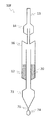
- FIG. 1 is a schematic diagram of the structure of a crucible for crystal growth in the first embodiment of the present invention
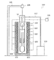
- FIG. 2 is a diagram showing an example of a schematic diagram of a semiconductor crystal growth apparatus in the first embodiment of the present invention
- FIG. 4 is a flow chart showing an example of a method for growing a semiconductor crystal using the crystal growth crucible of the present invention in the first embodiment of the present invention.
- FIG. 4 shows the state of the crystal growth crucible during initial distillation recovery in the first embodiment of the present invention and FIG. 5 is a schematic view showing an example of the movement of the raw material, FIG. 5 is a schematic view showing an example of the state of the crucible for crystal growth and the movement of the raw material during the main distillation recovery in the first embodiment of the present invention, and FIG. It is the schematic which shows an example of the state of the crucible for crystal growth at the time of completion
- the crucible 10 for crystal growth is roughly constituted by a holding part 12, a straight pipe part 13, an initial distillation collecting part 14, a main distillation condensing part 16, and a crystal growing part 18.
- the holding part 12 has a shape in which the upper end of the pipe part 17 connected to the crystal growing part 18 protrudes from below, and the holding part 12 protrudes from other parts by protruding from below.
- the raw material 20 is held in an isolated form.
- the initial distillation collecting unit 14 is a part that collects the initial distillation when the raw material 20 held in the holding unit 12 is vaporized, and the upper end of the pipe portion 15 connected to the holding unit 12 is the bottom of the initial distillation collecting unit 14. It has a more prominent shape.
- the diameter of the pipe part 15 is smaller than that of the pipe part 17, and since the pipe part 15 protrudes from the bottom of the initial distillation collecting part 14, the initial distillation collecting part 14 isolates the initial distillation 24 from other parts. Hold.
- the main distillation condensing unit 16 is a part that condenses the main distillation when the raw material 20 held in the holding unit 12 is vaporized, and is disposed between the initial distillation collecting unit 14 and a crystal growing unit 18 described later. Yes.
- the end of the pipe part 15 protrudes downward, and the raw material 26 condensed and liquefied in the lower convex part of the main distillation condensing part naturally falls by gravity, and passes through the pipe part 17. Collected by the crystal growing unit 18.
- the crystal growing unit 18 is a place where a main fraction 30 made of the raw material melt 28 condensed in the main distillation condensing unit 16 is held, and crystals are generated when growing the crystal from the held main fraction 30.
- the straight pipe portion 13 is a tubular portion that communicates with the vacuum exhaust pipe 112 (see FIG. 2) of the vacuum exhaust device 110 (see FIG. 2) for decompressing the inside of the crystal growing crucible 10. It is arranged above.
- the crystal growth apparatus 100 includes a crystal growth crucible 10 as shown in FIG. 1, a heating furnace 104 for heating the crystal growth crucible 10, an elevating device 108, and a vacuum exhaust apparatus. 110.
- the heating furnace 104 includes a multistage heater 102 capable of independently controlling the temperature of each part of the crystal growing crucible 10 (holding part 12, initial distillation collecting part 14, main distillation condensing part 16, crystal growing part 18), A heater control unit 106 that individually controls the temperature of the multistage heater 102 is provided.
- the lifting device 108 is a device for lifting and lowering the crystal growing crucible 10, and is supported by a support column 109. The crystal growing crucible 10 is suspended by the lifting device 108, and the crystal growing crucible 10 can be moved up and down as needed.
- the vacuum evacuation device 110 is a device for evacuating the inside of the crystal growth crucible 10, and is connected to the straight tube portion 13 of the crystal growth crucible 10 through a vacuum exhaust pipe 112.
- the temperature control unit for controlling the temperature of the crystal growth crucible 10 is roughly constituted by the heater 102, the heater control unit 106, and the lifting device 108.
- the raw material 20 is put into the holding part 12 of the crystal growth crucible 10 as shown in FIG.
- a method will be described in which the distillation fractions are separated by appropriately controlling the temperature of each part, and thereafter, crystals are grown using the highly purified main distillation.
- a series of steps will be described with reference to the flowchart of FIG. 3 and FIGS. 4 to 6.
- a crucible 10 for crystal growth as shown in FIG. 1 in which the upper end side of the straight pipe portion 13 is not sealed is prepared.
- the material of the crucible 10 is made of high-purity silica glass.
- the substrate is washed with hydrofluoric acid having a concentration of 5%, rinsed 5 times with pure water, and then dried (step S10).
- step S12 3 kg of a thallium bromide raw material is filled into the holding part 12 from the upper end side of the straight pipe part 13 of the crystal growing crucible 10 (step S12).
- the raw material 20 is charged as it is, it will fall to the crystal growing part 18, so a soft hose is inserted from the upper end side of the straight pipe part 13 of the crystal growing crucible 10, and the tip of the hose is connected to the holding part 12.
- Guide the raw material 20 through the hose.
- a powdery material for the raw material 20 it is easy to clog in the middle, so it is effective to put it in small quantities while giving vibration.
- thallium bromide is a highly toxic substance, so wear protective goggles, protective masks, impervious gloves, and work clothes that cover the whole body when working, and use exhaust ducts as necessary to prevent it from splashing around. It is desirable to perform this while sucking the vicinity of the work site.
- the crystal growth crucible 10 After completion of the filling of the raw material 20, the crystal growth crucible 10 is placed in the heating furnace 104 of the crystal growth apparatus 100 as shown in FIG. 2, and the crystal growth crucible 10 is connected to the lifting device 108 by hanging with a stainless steel wire. To do. In addition, if the load is applied only to the upper part of the crystal growing crucible 10, the crystal growing crucible 10 may be damaged without being able to withstand the excessive weight, so a wire is also wound around the lower part of the crystal growing part 18 and the holding part 12, The structure is such that a load is applied to the lower side of the crystal growing crucible 10.
- the vacuum exhaust pipe 12 is connected to the tip of the straight pipe portion 13 of the crystal growing crucible 10.
- the vacuum exhaust device 110 is equipped with a trap cooled with liquid nitrogen so that the vapor of the raw material 20 can be removed even when it is sucked.
- the vacuum evacuation device 110 is started, the inside of the crystal growing crucible 10 is evacuated, and is kept as it is for 1 hour, thereby removing components that volatilize at room temperature (step S14).
- thallium bromide is synthesized in an aqueous solution, so that there is a high possibility that a large amount of moisture is attached to the surface.
- the temperature of the entire crystal growth crucible 10 is gradually raised while evacuating in order to remove moisture (step S16). Specifically, the temperature is raised from room temperature to 100 ° C. in 1 hour while being evacuated by the evacuation apparatus 110, and held at 100 ° C. for 1 hour. Next, the temperature is raised to 300 ° C. over 1 hour and held at 300 ° C. for 1 hour. The higher the temperature, the easier it will be to remove the water, but at a much higher temperature, the vapor pressure of thallium bromide will increase and a large amount of evaporation will occur even if it is below the melting point, so it is desirable to keep it at an appropriate temperature. .
- step S18 the vicinity of the tip of the crystal growing crucible 10 is sealed with a burner (step S18).
- the sealing part is located below the portion connected to the vacuum exhaust pipe 112 of the straight pipe part 13, and the sealing work is performed while evacuating the inside.
- the inside of the crystal growing crucible 10 is kept in a vacuum or a reduced pressure state, and vacuum distillation can be performed by effectively using the vapor pressure of the raw material 20.
- the pressure inside the crucible 10 for crystal growth is preferably 500 Pa or less, and more preferably 100 Pa or less when the thallium bromide is 300 ° C.
- the vacuum exhaust device 110 is stopped.
- each temperature of the crystal growing unit 18, the holding unit 12, and the main distillation condensing unit 16 is set to be equal to or higher than the temperature of the initial distillation collecting unit 14.
- the heater control unit 106 is set so that the crystal growing unit 18, the holding unit 12, and the main distillation condensing unit 16 of the crystal growing crucible 10 are 600 ° C., and the initial distillation collecting unit 14 is 480 ° C.
- the temperature state is maintained for 30 minutes (step S20).
- the liquid that has become liquid in the initial distillation recovery unit 14 is subjected to the action of gravity while being attached to the inside of the crystal growing crucible 10 due to surface tension, and is guided to the bottom of the initial distillation recovery unit 14. Since the tube portion 15 connected to the holding portion 12 protrudes in the center of the initial distillation collecting portion 14, the tip thereof is higher than the bottom portion of the initial distillation collecting portion 14, so that a liquid state is formed between the two.
- the first 24 of is collected. Of the initial distillates 24, those that have become solid adhere to the wall surface of the crystal growth crucible 10 and remain there, so that they do not enter the crystal growth section 18. In addition, since the temperature of the crystal growing unit 18 is high, the vapor of the initial fraction 24 is not condensed in the crystal growing unit 18.
- the temperature of the initial distillation recovery unit 14 can be once lowered to 300 ° C., and the temperature of the other parts can be lowered to 480 ° C., and the process can be transferred to the next process after the next day. It is.
- the process proceeds to a recovery process of the main fraction 30 that leads the main fraction 30 with few impurities to the crystal growing unit 18.
- the temperature of the crystal growing part 18 and the main distillation condensing part 16 of the crystal growing crucible 10 is lowered to the vicinity of the melting point of the raw material 20.
- the heater temperature unit 106 is set so that the crystal growing unit 18 and the main distillation condensing unit 16 are 480 ° C.
- the holding unit 12 is 600 ° C.
- the initial distillation collecting unit 14 is 300 ° C. This state is maintained for 5 hours (step S24).
- step S24 the vapor generated from the raw material 20 (the white arrow in FIG. 5) condenses in the main distillation condensing unit 16 and at the latest in the pipe unit 15 before reaching the initial distillation collecting unit 14 to be liquid (condensed). It becomes the raw material 26) and adheres to the tube wall inside the main distillation agglomeration part 16 of the crucible 10 for crystal growth.
- the adhering condensing material 26 travels down the convex wall surface of the main distillation condensing unit 16 and moves to the center, finally falls as a droplet 28, and is led to the crystal growing unit 18 through the tube unit 17. (State shown in FIG. 5).
- the main tail 30 having the least amount of impurities can be recovered to the crystal growing unit 18. Further, since there is no need to seal the pipe connecting the main distillation condensing unit 16 and the initial distillation collecting unit 14, it is possible to shift from the recovery process of the initial distillation 24 to the recovery process of the main distillation 30 safely and efficiently. .
- the speed of distillation can be raised by raising the temperature of the holding
- the distillation rate is increased without lowering the purity of the main distillation 30, the partial pressure of gas components other than the raw material 20 in the crystal growth crucible 10 is reduced as much as possible, and most of the gas in the crystal growth crucible 10 is reduced. It is desirable that the raw material 20 is composed of steam.
- the heater control unit 106 is set so that the temperature of the holding unit 12 hardly evaporates with the raw material 20 remaining in the holding unit 12 to some extent, specifically, the temperature of the holding unit 12 is lowered to 480 ° C. Then, the collection of the main stream 30 is finished (step S26, the state shown in FIG. 6).
- the raw material 20 is left to some extent in the holding unit 12, but the amount thereof is generally about 10% of the input amount of the raw material 20.
- the raw material 20 is preferably left in the holding part 12 to some extent.
- step S28 the crystal growing crucible 10 is raised using the lifting device 108 until the crystal growing unit 18 comes to the position of the holding unit 12 (step S28).
- the initial distillation collecting unit 14 goes out of the heating furnace 104 and the temperature is lowered to around room temperature, and the main distillation condensing unit 16 and the holding unit 12 are at 300 ° C. Therefore, the raw material 20 remaining in these parts is solidified below the melting point, and there is no possibility of moving to other parts.
- the heater control unit 106 is set so that the space below the crystal growth unit 18 generated by raising the crystal growth crucible 10 is 370 ° C. and the crystal growth unit 18 is 480 ° C. (step S30). Crystal growth is started in the crystal growth unit 18 using this temperature difference.
- the crucible 10 for crystal growth is lowered using the lifting device 108, and the liquid main pool 30 is cooled from the lower part of the crucible 10 for crystal growth and solidified (step S32).
- the descending speed of the crystal growth crucible 10 at this time is, for example, 0.1 to 2 mm per hour. The smaller the descent speed, the easier it is to obtain good quality crystals. However, since the descent time is extended, it is appropriate that the production rate is about 0.5 to 1 mm per hour.
- the main tail 30 with few impurities can be recovered to the crystal growth unit 18.
- the main fraction 30 can be transferred to the crystal growth step without being exposed to the atmosphere.
- the crystal growing crucible 10 is broken to take out the crystal ingot inside (step S34). At that time, pay attention not to apply as much force as possible to the crystal, and wear protective gloves in a clean bench with a sufficient air flow so as not to suck in thallium bromide dust.
- the crystal ingot was light yellow and transparent, and the initial distillation was light yellow and opaque.
- the residue of the holding part 12 was brown and opaque, and each exhibited a color tone reflecting the amount of impurities.
- the inside of the crystal ingot is generally a single crystal, and sometimes a crystal interface was observed due to the simultaneous growth of multiple crystal nuclei, but even in that case, the number of crystals seen when observed from the top of the crystal ingot is The number was 5 or less.
- it when it is used for a detector, it is a small piece of several millimeters square, so it can be used avoiding the crystal interface.
- the crystal ingot be a single crystal having no crystal interface as much as possible.
- the holding unit 12 that holds the raw material 20 as the crystal growth crucible 10 used for crystal growth.
- the initial distillation collecting unit 14 that collects the initial distillation 24 when the raw material 20 held in the holding unit 12 is vaporized, and the main distillation that condenses the main distillation when the raw material 20 held in the holding unit 12 is vaporized.
- the raw material 20 can be efficiently and sufficiently purified, and a high-quality semiconductor crystal can be manufactured with high efficiency.
- FIG. 7 is a schematic diagram of the structure of the crucible for crystal growth in the second embodiment of the present invention.
- the crystal growth crucible 10A according to the second embodiment of the present invention is arranged on the main distillation condensing section 16 side of the holding section 12.
- a distillation packing 42 is provided on an upper side.
- the distillation packing 42 has a large surface area and is made of an inert material, such as silica glass. Although the cross-sectional shape of the packing 42 for distillation is substantially circular in FIG. 7, it is not limited to this shape. Any other inert material can be used for the packing for distillation 42, but when a material having a higher density than the raw material to be filled in the holding unit 12 is used, the packing for distillation 42 is used as a raw material. A mechanism for holding it at the top is required, and for example, a method such as inserting a table can be mentioned.
- the configuration other than the provision of the packing for distillation 42 is substantially the same as that of the crucible 10 for crystal growth of the first embodiment, and the details are omitted.
- the heater control unit 106 When performing the recovery process of the initial distillation 24 and the main distillation recovery process using the crucible 10A for crystal growth, the temperature of the portion close to the holding portion 12 of the packing for distillation 42 is increased, the upper end of the packing for distillation 42, That is, the heater control unit 106 is set so that the temperature decreases as it approaches the main distillation condensing unit 16.
- a crucible 10A for crystal growth as shown in FIG. 7 is prepared.
- a number of silica glass short tubes are prepared as the distillation filler 42 of the crystal growing crucible 10A.
- the distillation packing 42 is charged.
- the crystal growth portion 18 and the holding portion 12 of the crystal growth crucible 10A are 600 ° C.
- the upper end of the packing for distillation 42 is 480 ° C.
- the main distillation condensing portion 16 is 520 ° C.
- the initial distillation recovery portion 14. Is set so that the temperature becomes 480 ° C. and held for 1 hour.
- the movement of the steam to the initial distillation collecting unit 14 is delayed, so that the holding time needs to be longer than that in the initial distillation collecting step in the first embodiment.
- the crystal growing portion 18 of the crystal growing crucible 10A, the upper end of the distillation packing 42 and the main distillation condensing portion 16 are 480 ° C.
- the holding portion 12 is 600 ° C.
- the initial distillation collecting portion 14 is 300 ° C.
- the heater control unit 106 is set so as to be at ° C., and is held for 10 hours. Subsequent steps are the same as those in the first embodiment.
- the raw material 20 can be efficiently and sufficiently purified, and a high-quality semiconductor crystal can be manufactured with high efficiency.
- the vapor generated and raised in the holding unit 12 is condensed again in the packing for distillation 42 to become a liquid, and is lowered by the action of gravity. Then, it evaporates again due to the high temperature of the holding part 12 while descending. In this manner, the evaporation and liquefaction of the raw material 20 can be repeatedly generated. Since the separation effect of impurities in distillation occurs during the phase change between gas and liquid, the separation efficiency improves as the number of evaporation and liquefaction increases, and it is possible to obtain a higher purity crystal growth become.
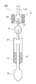
- FIG. 8 is a schematic view of the structure of a crucible for crystal growth in the third embodiment of the present invention.
- the crucible 10B for crystal growth in the third embodiment of the present invention has a straight pipe portion 13A on the upper part of the initial distillation collecting portion 14 in addition to the structure of the crucible 10 for crystal growth of the first embodiment.
- a coaxial cold trap 52 is provided.
- the coaxial cold trap 52 has a trap portion 53 for effectively removing impurities having a low boiling point, such as water and silicon bromide, and a cooling portion 54 for cooling the trap portion 53. .
- impurities having a low boiling point such as water and silicon bromide
- the configuration other than the coaxial cold trap 52 is substantially the same as the crystal growth crucible 10 of the first embodiment, and the details are omitted.
- a crucible 10B for crystal growth as shown in FIG. 8 is prepared.
- the crystal growth part 18, the holding part 12, and the main distillation condensing part 16 of the crystal growth crucible 10B are initially heated at 600 ° C.
- the heater control unit 106 is set so that the distillation collection unit 14 is 480 ° C., and the temperature of the cooling unit 54 is controlled so that the trap unit 53 of the coaxial cold trap 52 is ⁇ 20 ° C., and is held for 30 minutes.
- white solid accumulates in the trap portion 53 of the coaxial cold trap 52, but the amount of the white solid covers the wall surface.
- the process proceeds to a main distillation collecting step, and a heater control unit is set so that the crystal growing unit 18 and the main distillation condensing unit 16 of the crystal growing crucible 10B are 480 ° C., the holding unit 12 is 600 ° C., and the initial distillation collecting unit 14 is 300 ° C. 106 is set, and the temperature of the cooling section 54 is controlled so that the trap section 53 of the coaxial cold trap 52 becomes minus 20 ° C., and is held for 5 hours. During this time, accumulation of white solid continued in the trap portion 53 of the coaxial cold trap 52. Thereafter, the same steps as in the first embodiment are performed.
- the raw material 20 can be efficiently and sufficiently purified, and a high-quality semiconductor crystal can be manufactured with high efficiency.
- the coaxial cold trap 52 can effectively remove impurities having a low boiling point, such as water and silicon bromide, and can further reduce the impurity concentration of the crystal to be grown.
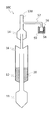
- FIG. 9 is a schematic view of the structure of a crystal growth crucible in the fourth embodiment of the present invention.
- the crystal growth crucible 10C according to the fourth embodiment of the present invention includes a parallel cold on the side of the initial distillation recovery unit 14 in addition to the configuration of the crystal growth crucible 10 of the first embodiment.
- a trap 56 is provided.
- the parallel cold trap 56 is disposed on the side of the initial distillation collecting unit 14, a parallel pipe 57 having one end connected to the straight pipe part 13B, a trap part 58 connected to the other end of the parallel pipe 57, A cooling part 59 for cooling the trap part 58 is provided.
- the configuration other than the parallel cold trap 56 is substantially the same as the crucible 10 for crystal growth of the first embodiment, and the details are omitted.
- a crucible 10C for crystal growth as shown in FIG. 9 is prepared.
- the crystal growth part 18, the holding part 12, and the main distillation condensing part 16 of the crystal growth crucible 10C are initially heated at 600 ° C.
- the heater control unit 106 is set so that the distillation collection unit 14 is 480 ° C., and the temperature of the cooling unit 59 is controlled so that the trap unit 58 of the parallel cold trap 56 is ⁇ 40 ° C., and is held for 30 minutes.
- white solid accumulates in the trap portion 58 of the parallel cold trap 56, but the amount of the white solid covers the wall surface.
- the process proceeds to a main distillation recovery step, and the heater control is performed so that the crystal growth unit 18 and the main distillation condensing unit 16 of the crucible 10C for crystal growth are 480 ° C., the holding unit 12 is 600 ° C., and the initial distillation recovery unit 14 is 300 ° C.
- the temperature of the cooling unit 59 is controlled so that the trap unit 58 of the parallel cold trap 56 becomes ⁇ 40 ° C. and held for 5 hours. During this time, accumulation of white solid continued in the trap portion 58 of the parallel cold trap 56. Thereafter, the same steps as in the first embodiment are performed.
- the raw material 20 can be efficiently and sufficiently purified, and a high-quality semiconductor crystal can be manufactured with high efficiency.
- the parallel cold trap 56 by cooling the parallel cold trap 56 to 0 ° C. or lower, impurities having a low boiling point, such as water and silicon bromide, can be effectively removed as in the third embodiment.
- impurities having a low boiling point such as water and silicon bromide
- the parallel cold trap 56 is installed on the side of the initial distillation recovery unit 14, the influence of the high temperature air rising from the heating furnace 104 can be suppressed, and the temperature of the parallel cold trap 56 can be further increased. Easy to lower. Therefore, it is possible to improve the recovery rate of impurities having a low boiling point or to operate even when the performance of the cooling unit 59 is low, and it is possible to further reduce the impurity concentration of the crystal to be grown.
- FIG. 10 is a schematic diagram of the structure of the crucible for crystal growth in the fifth embodiment of the present invention.
- a crucible for crystal growth 10D includes a zone refining section 62 and a movable heater instead of the crystal growth section 18 of the crystal growth crucible 10 of the first embodiment.
- the crystal growth part 61 which further has 64 is provided.
- the crucible 10D for crystal growth of this embodiment has a thick zone purification unit 62 for performing zone purification in the crystal growth unit 61, and is installed vertically to collect the main distillation. After being performed, the zone is refined by being laid sideways and heated by the movable heater 64.
- the configuration other than the crystal growth unit 61 is substantially the same as the crystal growth crucible 10 of the first embodiment, and the details are omitted.
- the temperature of the entire crystal growth crucible 10D is gradually cooled to 40 ° C. or lower and taken out from the heating furnace 104. Thereafter, the crystal growing crucible 10D is placed sideways, and the temperature of the movable heater 64 is set to 600 ° C. When the temperature of the movable heater 64 reaches 600 ° C., the tip (right side of FIG. 10) of the zone refining unit 62 of the crystal growing unit 61 is heated to melt the internal solid, and the movable heater 64 is gradually moved to the left in FIG. To spread the contents evenly.
- the movable heater 64 is moved from one end to the other end at a speed of 2 mm per hour, and this is repeated several times to perform zone purification. Finally, the movable heater 64 is moved at a speed of 0.5 mm per hour to grow crystals.
- all of Mg, Na, Zn, which are easily evaporated impurity elements, and Ti, Mn, O, which are easily evaporated impurities are 0.5 ppm or less. there were. About Si, it was 3 ppm or less. However, As was 1 ppm or less.
- the raw material 20 can be efficiently and sufficiently purified, and a high-quality semiconductor crystal can be manufactured with high efficiency.
- the distilled raw material can be used for zone purification without contacting the outside, it is very suitable for growing crystals of higher purity.
- the phase change between the solid and the liquid As is easily taken into the solid side of thallium bromide and is difficult to remove by zone purification. Therefore, it is desirable to remove it sufficiently in the distillation step.
- FIG. 11 is a schematic view of the structure of the crucible for crystal growth in the sixth embodiment of the present invention.
- the crystal growth crucible 10E according to the sixth embodiment of the present invention has a seed crystal generation in the lower portion of the crystal growth portion 71 in addition to the structure of the crystal growth crucible 10 of the first embodiment.
- the unit 72 is provided.
- the seed crystal generating part 72 is a thin tubular part disposed at the lower part of the crystal growing part 71 as shown in FIG.
- the configuration other than the seed crystal generation unit 72 is substantially the same as the crystal growth crucible 10 of the first embodiment, and the details are omitted.
- the crystal growth crucible 10E as shown in FIG. 11 is used until the main distillation collecting step, and then the crystal is grown using the lifting device 108 of the crystal growth device 100 until the seed crystal generation unit 72 comes to the position of the holding unit 12. Raise the crucible 10E for raising. Then, the crucible 10E for crystal growth is lowered using the lifting device 108, and the liquid main distillation is cooled and solidified from the lower part of the crucible 10E for crystal growth.
- the descending speed of the crystal growth crucible 10E is 0.1 to 2 mm per hour.
- the obtained crystal ingot had many single crystals, and even when a crystal interface was present, the number of crystals observed when observed from the upper end of the crystal ingot was 3 or less.
- the same effect as that of the first embodiment of the crystal growth crucible described above can be obtained. That is, the raw material 20 can be efficiently and sufficiently purified, and a high-quality semiconductor crystal can be manufactured with high efficiency.
- the seed crystal generation unit 72 since the seed crystal generation unit 72 is provided, when the seed crystal generation unit 72 generates a seed crystal at the time of crystal growth, the largest grown crystal enters the crystal growth unit 71, and serves as a base point. Furthermore, it is possible to obtain a single crystal more reliably by further promoting crystal growth.
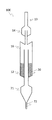
- FIG. 12 is a schematic view of the structure of the crystal growing crucible in the seventh embodiment of the present invention.
- the crucible for crystal growth 10F includes a seed crystal selection section at the lower part of the crystal growth section 73 in addition to the structure of the crystal growth crucible 10 of the first embodiment. 76, and a seed crystal generation unit 74 under the seed crystal selection unit 76.
- the seed crystal selection unit 76 is a thin tubular portion provided below the crystal growth unit 73, and the seed crystal generation unit 74 has a diameter larger than that of the seed crystal selection unit 76 provided below the seed crystal selection unit 76. It is a thick tubular part.
- the configuration other than the seed crystal selection unit 76 and the seed crystal generation unit 74 is substantially the same as the crucible 10 for crystal growth of the first embodiment, and the details are omitted.
- the crystal growth crucible 10F as shown in FIG. 12 is used to perform the main distillation collecting step, and then the crystal is grown using the lifting device 108 of the crystal growth device 100 until the seed crystal generation unit 74 comes to the position of the holding unit 12. Raise the crucible 10F for raising. Next, the crucible 10F for crystal growth is lowered using the lifting device 108, and the liquid main distillation is cooled and solidified from the lower part of the crucible 10F for crystal growth.
- the descending speed of the crystal growth crucible 10F is 0.1 to 2 mm per hour.
- the obtained crystal ingot was a single crystal in most cases, and even when a crystal interface was present, the number of crystals seen when observed from the upper end of the crystal ingot was 2 or less.
- the same effect as that of the first embodiment of the crystal growth crucible described above can be obtained. That is, the raw material 20 can be efficiently and sufficiently purified, and a high-quality semiconductor crystal can be manufactured with high efficiency.
- the number of seed crystals generated in the seed crystal generation unit 74 at the time of crystal growth is not limited to one, but by installing the thin seed crystal selection unit 76, only the seed crystal that has reached the lower end of the seed crystal selection unit 76 can be obtained. It can lead to the crystal growth part 73, and the possibility that the resulting crystal ingot becomes a single crystal can be further increased.
- FIG. 13 is a schematic view of the structure of a crystal growing crucible in the eighth embodiment of the present invention.
- the crucible 10G for crystal growth according to the eighth embodiment of the present invention is provided with a cooling rod 82 below the crystal growth portion 81 in addition to the structure of the crystal growth crucible 10 of the first embodiment. Is provided.
- the cooling rod 82 is a portion connected to the lower end of the crystal growing portion 81, and is provided to more reliably cool the lower end of the crystal growing portion 81 during crystal growth.
- the configuration other than the cooling rod 82 is substantially the same as the crystal growth crucible 10 of the first embodiment, and the details are omitted.
- the crystal growth device 100 After performing the final distillation collecting step using the crystal growth crucible 10G as shown in FIG. 13, until the cooling rod 82 comes to the position of the holding unit 12, the crystal growth device 100 is used for the crystal growth. Raise crucible 10G. Next, the crystal growing crucible 10G is lowered using the lifting device 108, and the liquid main distillation is cooled and solidified from the lower portion of the crystal growing crucible 10G. The descending speed of the crystal growth crucible 10G is 0.1 to 2 mm per hour.
- the obtained crystal ingot had many single crystals, and even when a crystal interface was present, the number of crystals observed when observed from the upper end of the crystal ingot was 3 or less.
- the raw material 20 can be efficiently and sufficiently purified, and a high-quality semiconductor crystal can be manufactured with high efficiency.
- the provision of the cooling rod 82 makes it easier to maintain the temperature gradient at the lower and upper portions of the crystal growing portion 81, and it is possible to more reliably obtain a crystal ingot with fewer crystal interfaces.
- FIG. 14 is a schematic view of the structure of a crystal growing crucible in the ninth embodiment of the present invention.
- the crystal growth crucible 10H according to the ninth embodiment of the present invention has a structure in which the main distillation condensing part 96 does not have a downward convex structure as compared with the crystal growth crucible 10 of the first embodiment. It is a structure.
- the crucible 10H for crystal growth of this example does not have a downward convex structure for the main distillation condensing unit 96 to guide the main distillation to the crystal growing unit 91.
- the holding unit 92 and the main distillation condensing unit 96 are arranged so that the main distillation condensed by the main distillation condensing unit 96 is guided to the crystal growing unit 91 through the conduit 97 by gravity. It is what.
- a crystal growth crucible 10H as shown in FIG. 14 and a crystal growth apparatus provided with a heating furnace configured to change the installation angle are prepared.
- the prepared crystal growth crucible 10H is inserted and fixed to the heating furnace so as to be inclined, and the initial distillation recovery process and the main distillation recovery process are performed.
- the temperature setting conditions at this time are the same as those in the first embodiment. Thereafter, the crystal growth crucible 10H is placed vertically to perform crystal growth.
- the inside of the crystal ingot is generally a single crystal, and sometimes a crystal interface is observed due to the simultaneous growth of a plurality of crystal nuclei, but even in this case, the crystal seen when observed from the upper end of the crystal ingot was 5 or less.
- the raw material 20 can be efficiently and sufficiently purified, and a high-quality semiconductor crystal can be manufactured with high efficiency.
- the crystal to be grown is not limited to this, and for example, for growing various crystals such as cadmium telluride, cadmium / zinc / tellurium, gallium arsenide, and the like.
- the present invention is applicable.
Landscapes
- Chemical & Material Sciences (AREA)
- Organic Chemistry (AREA)
- Engineering & Computer Science (AREA)
- Crystallography & Structural Chemistry (AREA)
- Materials Engineering (AREA)
- Metallurgy (AREA)
- Inorganic Chemistry (AREA)
- Crystals, And After-Treatments Of Crystals (AREA)
Priority Applications (3)
| Application Number | Priority Date | Filing Date | Title |
|---|---|---|---|
| EP14883763.6A EP3112503A4 (en) | 2014-02-27 | 2014-10-08 | Crucible for crystal growth, crystal growth apparatus provided therewith, and method for growing crystals |
| CN201480076252.0A CN106062258B (zh) | 2014-02-27 | 2014-10-08 | 晶体培养用坩埚、具备该晶体培养用坩埚的晶体培养装置以及晶体培养方法 |
| US15/116,532 US20160348270A1 (en) | 2014-02-27 | 2014-10-08 | Crucible for crystal growth, crystal growing apparatus provided therewith, and method for growing crystals |
Applications Claiming Priority (2)
| Application Number | Priority Date | Filing Date | Title |
|---|---|---|---|
| JP2014-036375 | 2014-02-27 | ||
| JP2014036375A JP6162625B2 (ja) | 2014-02-27 | 2014-02-27 | 結晶育成用るつぼおよびそれを備えた結晶育成装置ならびに結晶育成方法 |
Publications (1)
| Publication Number | Publication Date |
|---|---|
| WO2015129091A1 true WO2015129091A1 (ja) | 2015-09-03 |
Family
ID=54008437
Family Applications (1)
| Application Number | Title | Priority Date | Filing Date |
|---|---|---|---|
| PCT/JP2014/077016 Ceased WO2015129091A1 (ja) | 2014-02-27 | 2014-10-08 | 結晶育成用るつぼおよびそれを備えた結晶育成装置ならびに結晶育成方法 |
Country Status (5)
| Country | Link |
|---|---|
| US (1) | US20160348270A1 (enExample) |
| EP (1) | EP3112503A4 (enExample) |
| JP (1) | JP6162625B2 (enExample) |
| CN (1) | CN106062258B (enExample) |
| WO (1) | WO2015129091A1 (enExample) |
Cited By (1)
| Publication number | Priority date | Publication date | Assignee | Title |
|---|---|---|---|---|
| CN106191785A (zh) * | 2016-09-27 | 2016-12-07 | 京东方科技集团股份有限公司 | 坩埚、蒸镀装置及蒸镀系统 |
Families Citing this family (2)
| Publication number | Priority date | Publication date | Assignee | Title |
|---|---|---|---|---|
| WO2018039583A1 (en) * | 2016-08-26 | 2018-03-01 | Northwestern University | Methods for the synthesis, purification and crystal growth of inorganic crystals for hard radiation detectors |
| CN116516461A (zh) * | 2018-11-22 | 2023-08-01 | 北京滨松光子技术股份有限公司 | 一种溴化铊半导体单晶的生长方法及设备 |
Citations (8)
| Publication number | Priority date | Publication date | Assignee | Title |
|---|---|---|---|---|
| GB997402A (en) * | 1960-10-12 | 1965-07-07 | Knapsack Ag | Thermal process of preparing magnesium |
| JPS61201690A (ja) * | 1985-03-04 | 1986-09-06 | Nippon Telegr & Teleph Corp <Ntt> | 化合物半導体単結晶の育成方法および育成装置 |
| JPS63291819A (ja) * | 1987-05-26 | 1988-11-29 | Mitsubishi Metal Corp | ガリウムの回収方法 |
| JP2002286847A (ja) * | 2001-03-22 | 2002-10-03 | Reitekku:Kk | 半導体放射線検出装置 |
| JP2004075557A (ja) * | 2002-08-12 | 2004-03-11 | Sugai Chemical Industry Co Ltd | アダマンタノンの精製方法 |
| JP2008189483A (ja) * | 2007-02-01 | 2008-08-21 | Morita Kagaku Kogyo Kk | フッ化水素酸、塩酸およびケイフッ化水素酸を含有する廃液から酸成分を分離・回収する方法およびその装置 |
| JP2009256119A (ja) * | 2008-04-14 | 2009-11-05 | Hitachi Chem Co Ltd | 原料蒸留用器具、及び、シンチレータ用結晶の製造方法 |
| JP2011225742A (ja) * | 2010-04-21 | 2011-11-10 | Hitachi Chem Co Ltd | 原料精製装置およびシンチレータ用単結晶の製造方法 |
Family Cites Families (6)
| Publication number | Priority date | Publication date | Assignee | Title |
|---|---|---|---|---|
| JPS55121999A (en) * | 1979-03-15 | 1980-09-19 | Shiro Sakuragi | Preparing high-purity metal halide |
| JPH0710674A (ja) * | 1993-06-23 | 1995-01-13 | Mitsubishi Chem Corp | 無機化合物単結晶成長方法 |
| CN100516319C (zh) * | 2007-12-19 | 2009-07-22 | 华中科技大学 | 一种无籽晶垂直气相生长溴化铊单晶方法 |
| CN100516318C (zh) * | 2007-12-19 | 2009-07-22 | 华中科技大学 | 一种自发成核生长溴化铊单晶方法 |
| DE102010044017B4 (de) * | 2010-11-17 | 2013-06-20 | Carl Zeiss Smt Gmbh | Verfahren zur Herstellung von Alkali- oder Erdalkalifluorid-Kristallen und nach dem Verfahren hergestellte Kristalle |
| US8512470B2 (en) * | 2011-04-08 | 2013-08-20 | China Crystal Technologies Co. Ltd | System and methods for growing high-resistance single crystals |
-
2014
- 2014-02-27 JP JP2014036375A patent/JP6162625B2/ja not_active Expired - Fee Related
- 2014-10-08 CN CN201480076252.0A patent/CN106062258B/zh not_active Expired - Fee Related
- 2014-10-08 EP EP14883763.6A patent/EP3112503A4/en not_active Withdrawn
- 2014-10-08 WO PCT/JP2014/077016 patent/WO2015129091A1/ja not_active Ceased
- 2014-10-08 US US15/116,532 patent/US20160348270A1/en not_active Abandoned
Patent Citations (8)
| Publication number | Priority date | Publication date | Assignee | Title |
|---|---|---|---|---|
| GB997402A (en) * | 1960-10-12 | 1965-07-07 | Knapsack Ag | Thermal process of preparing magnesium |
| JPS61201690A (ja) * | 1985-03-04 | 1986-09-06 | Nippon Telegr & Teleph Corp <Ntt> | 化合物半導体単結晶の育成方法および育成装置 |
| JPS63291819A (ja) * | 1987-05-26 | 1988-11-29 | Mitsubishi Metal Corp | ガリウムの回収方法 |
| JP2002286847A (ja) * | 2001-03-22 | 2002-10-03 | Reitekku:Kk | 半導体放射線検出装置 |
| JP2004075557A (ja) * | 2002-08-12 | 2004-03-11 | Sugai Chemical Industry Co Ltd | アダマンタノンの精製方法 |
| JP2008189483A (ja) * | 2007-02-01 | 2008-08-21 | Morita Kagaku Kogyo Kk | フッ化水素酸、塩酸およびケイフッ化水素酸を含有する廃液から酸成分を分離・回収する方法およびその装置 |
| JP2009256119A (ja) * | 2008-04-14 | 2009-11-05 | Hitachi Chem Co Ltd | 原料蒸留用器具、及び、シンチレータ用結晶の製造方法 |
| JP2011225742A (ja) * | 2010-04-21 | 2011-11-10 | Hitachi Chem Co Ltd | 原料精製装置およびシンチレータ用単結晶の製造方法 |
Cited By (2)
| Publication number | Priority date | Publication date | Assignee | Title |
|---|---|---|---|---|
| CN106191785A (zh) * | 2016-09-27 | 2016-12-07 | 京东方科技集团股份有限公司 | 坩埚、蒸镀装置及蒸镀系统 |
| WO2018059019A1 (zh) * | 2016-09-27 | 2018-04-05 | 京东方科技集团股份有限公司 | 坩埚、蒸镀装置及蒸镀系统 |
Also Published As
| Publication number | Publication date |
|---|---|
| EP3112503A4 (en) | 2017-08-23 |
| JP6162625B2 (ja) | 2017-07-12 |
| JP2015160771A (ja) | 2015-09-07 |
| CN106062258A (zh) | 2016-10-26 |
| EP3112503A1 (en) | 2017-01-04 |
| CN106062258B (zh) | 2018-05-29 |
| US20160348270A1 (en) | 2016-12-01 |
Similar Documents
| Publication | Publication Date | Title |
|---|---|---|
| JP6162625B2 (ja) | 結晶育成用るつぼおよびそれを備えた結晶育成装置ならびに結晶育成方法 | |
| US20120171848A1 (en) | Method and System for Manufacturing Silicon and Silicon Carbide | |
| JP5859577B2 (ja) | シリコン精製装置及びシリコン精製方法 | |
| JP6602833B2 (ja) | 希土類金属及希土類金属の精製方法 | |
| TWI542705B (zh) | Production method of high purity calcium | |
| JP5291028B2 (ja) | アルミニウム材およびその製造方法 | |
| US20020022088A1 (en) | Purified silicon production system | |
| JP3842851B2 (ja) | インジウムの精製方法 | |
| KR101669444B1 (ko) | 액상 기법을 이용한 SiC 단결정 성장 방법 | |
| JP5992244B2 (ja) | 高純度マグネシウムの製造方法及び高純度マグネシウム | |
| JP2015160771A5 (enExample) | ||
| CN104245581A (zh) | 硅提纯装置和硅提纯方法 | |
| JP2017186211A (ja) | 結晶育成用るつぼおよびそれを備えた結晶育成装置ならびに結晶育成方法 | |
| JP2011225742A (ja) | 原料精製装置およびシンチレータ用単結晶の製造方法 | |
| Tonn et al. | Removal of oxidic impurities for the growth of high purity lead iodide single crystals | |
| CN100408731C (zh) | 用碘化铅熔体生长单晶体的方法 | |
| JP2006283192A (ja) | 高純度インジウム | |
| CN105696081B (zh) | 锑化铝材料的制备方法 | |
| US10370253B2 (en) | Silicon refining device | |
| JP2018203586A (ja) | 臭化タリウム製品製造方法及び装置 | |
| WO2016046983A1 (ja) | 結晶成長方法 | |
| Stowe et al. | Synthesis of a potential semiconductor neutron detector crystal LiGa (Se/Te) 2: Materials purity and compatibility effects | |
| JP2012076944A (ja) | シリコン精製装置及びシリコン精製方法 | |
| Yoshida et al. | Purification of Metallurgical-Grade Silicon by Solvent Refining Using Si–Zn Alloy: Yoshida, Norikawa, and Nohira | |
| JPH10121160A (ja) | 高純度亜鉛の製造方法および製造装置 |
Legal Events
| Date | Code | Title | Description |
|---|---|---|---|
| 121 | Ep: the epo has been informed by wipo that ep was designated in this application |
Ref document number: 14883763 Country of ref document: EP Kind code of ref document: A1 |
|
| WWE | Wipo information: entry into national phase |
Ref document number: 15116532 Country of ref document: US |
|
| REEP | Request for entry into the european phase |
Ref document number: 2014883763 Country of ref document: EP |
|
| WWE | Wipo information: entry into national phase |
Ref document number: 2014883763 Country of ref document: EP |
|
| NENP | Non-entry into the national phase |
Ref country code: DE |