WO2015125587A1 - 光電変換素子及び太陽電池 - Google Patents
光電変換素子及び太陽電池 Download PDFInfo
- Publication number
- WO2015125587A1 WO2015125587A1 PCT/JP2015/052684 JP2015052684W WO2015125587A1 WO 2015125587 A1 WO2015125587 A1 WO 2015125587A1 JP 2015052684 W JP2015052684 W JP 2015052684W WO 2015125587 A1 WO2015125587 A1 WO 2015125587A1
- Authority
- WO
- WIPO (PCT)
- Prior art keywords
- photoelectric conversion
- conversion element
- transport layer
- hole transport
- electrode
- Prior art date
- Legal status (The legal status is an assumption and is not a legal conclusion. Google has not performed a legal analysis and makes no representation as to the accuracy of the status listed.)
- Ceased
Links
Images
Classifications
-
- H—ELECTRICITY
- H10—SEMICONDUCTOR DEVICES; ELECTRIC SOLID-STATE DEVICES NOT OTHERWISE PROVIDED FOR
- H10K—ORGANIC ELECTRIC SOLID-STATE DEVICES
- H10K71/00—Manufacture or treatment specially adapted for the organic devices covered by this subclass
- H10K71/30—Doping active layers, e.g. electron transporting layers
-
- H—ELECTRICITY
- H10—SEMICONDUCTOR DEVICES; ELECTRIC SOLID-STATE DEVICES NOT OTHERWISE PROVIDED FOR
- H10K—ORGANIC ELECTRIC SOLID-STATE DEVICES
- H10K85/00—Organic materials used in the body or electrodes of devices covered by this subclass
- H10K85/60—Organic compounds having low molecular weight
- H10K85/631—Amine compounds having at least two aryl rest on at least one amine-nitrogen atom, e.g. triphenylamine
- H10K85/636—Amine compounds having at least two aryl rest on at least one amine-nitrogen atom, e.g. triphenylamine comprising heteroaromatic hydrocarbons as substituents on the nitrogen atom
-
- H—ELECTRICITY
- H01—ELECTRIC ELEMENTS
- H01G—CAPACITORS; CAPACITORS, RECTIFIERS, DETECTORS, SWITCHING DEVICES, LIGHT-SENSITIVE OR TEMPERATURE-SENSITIVE DEVICES OF THE ELECTROLYTIC TYPE
- H01G9/00—Electrolytic capacitors, rectifiers, detectors, switching devices, light-sensitive or temperature-sensitive devices; Processes of their manufacture
- H01G9/20—Light-sensitive devices
- H01G9/2004—Light-sensitive devices characterised by the electrolyte, e.g. comprising an organic electrolyte
- H01G9/2018—Light-sensitive devices characterised by the electrolyte, e.g. comprising an organic electrolyte characterised by the ionic charge transport species, e.g. redox shuttles
-
- H—ELECTRICITY
- H01—ELECTRIC ELEMENTS
- H01G—CAPACITORS; CAPACITORS, RECTIFIERS, DETECTORS, SWITCHING DEVICES, LIGHT-SENSITIVE OR TEMPERATURE-SENSITIVE DEVICES OF THE ELECTROLYTIC TYPE
- H01G9/00—Electrolytic capacitors, rectifiers, detectors, switching devices, light-sensitive or temperature-sensitive devices; Processes of their manufacture
- H01G9/20—Light-sensitive devices
- H01G9/2027—Light-sensitive devices comprising an oxide semiconductor electrode
-
- H—ELECTRICITY
- H01—ELECTRIC ELEMENTS
- H01G—CAPACITORS; CAPACITORS, RECTIFIERS, DETECTORS, SWITCHING DEVICES, LIGHT-SENSITIVE OR TEMPERATURE-SENSITIVE DEVICES OF THE ELECTROLYTIC TYPE
- H01G9/00—Electrolytic capacitors, rectifiers, detectors, switching devices, light-sensitive or temperature-sensitive devices; Processes of their manufacture
- H01G9/20—Light-sensitive devices
- H01G9/2059—Light-sensitive devices comprising an organic dye as the active light absorbing material, e.g. adsorbed on an electrode or dissolved in solution
-
- H—ELECTRICITY
- H01—ELECTRIC ELEMENTS
- H01G—CAPACITORS; CAPACITORS, RECTIFIERS, DETECTORS, SWITCHING DEVICES, LIGHT-SENSITIVE OR TEMPERATURE-SENSITIVE DEVICES OF THE ELECTROLYTIC TYPE
- H01G9/00—Electrolytic capacitors, rectifiers, detectors, switching devices, light-sensitive or temperature-sensitive devices; Processes of their manufacture
- H01G9/20—Light-sensitive devices
- H01G9/209—Light trapping arrangements
-
- H—ELECTRICITY
- H10—SEMICONDUCTOR DEVICES; ELECTRIC SOLID-STATE DEVICES NOT OTHERWISE PROVIDED FOR
- H10K—ORGANIC ELECTRIC SOLID-STATE DEVICES
- H10K30/00—Organic devices sensitive to infrared radiation, light, electromagnetic radiation of shorter wavelength or corpuscular radiation
- H10K30/10—Organic devices sensitive to infrared radiation, light, electromagnetic radiation of shorter wavelength or corpuscular radiation comprising heterojunctions between organic semiconductors and inorganic semiconductors
- H10K30/15—Sensitised wide-bandgap semiconductor devices, e.g. dye-sensitised TiO2
- H10K30/151—Sensitised wide-bandgap semiconductor devices, e.g. dye-sensitised TiO2 the wide bandgap semiconductor comprising titanium oxide, e.g. TiO2
-
- H—ELECTRICITY
- H10—SEMICONDUCTOR DEVICES; ELECTRIC SOLID-STATE DEVICES NOT OTHERWISE PROVIDED FOR
- H10K—ORGANIC ELECTRIC SOLID-STATE DEVICES
- H10K30/00—Organic devices sensitive to infrared radiation, light, electromagnetic radiation of shorter wavelength or corpuscular radiation
- H10K30/10—Organic devices sensitive to infrared radiation, light, electromagnetic radiation of shorter wavelength or corpuscular radiation comprising heterojunctions between organic semiconductors and inorganic semiconductors
- H10K30/15—Sensitised wide-bandgap semiconductor devices, e.g. dye-sensitised TiO2
- H10K30/152—Sensitised wide-bandgap semiconductor devices, e.g. dye-sensitised TiO2 the wide bandgap semiconductor comprising zinc oxide, e.g. ZnO
-
- H—ELECTRICITY
- H10—SEMICONDUCTOR DEVICES; ELECTRIC SOLID-STATE DEVICES NOT OTHERWISE PROVIDED FOR
- H10K—ORGANIC ELECTRIC SOLID-STATE DEVICES
- H10K85/00—Organic materials used in the body or electrodes of devices covered by this subclass
- H10K85/60—Organic compounds having low molecular weight
- H10K85/649—Aromatic compounds comprising a hetero atom
- H10K85/654—Aromatic compounds comprising a hetero atom comprising only nitrogen as heteroatom
-
- H—ELECTRICITY
- H10—SEMICONDUCTOR DEVICES; ELECTRIC SOLID-STATE DEVICES NOT OTHERWISE PROVIDED FOR
- H10K—ORGANIC ELECTRIC SOLID-STATE DEVICES
- H10K85/00—Organic materials used in the body or electrodes of devices covered by this subclass
- H10K85/60—Organic compounds having low molecular weight
- H10K85/649—Aromatic compounds comprising a hetero atom
- H10K85/656—Aromatic compounds comprising a hetero atom comprising two or more different heteroatoms per ring
-
- H—ELECTRICITY
- H10—SEMICONDUCTOR DEVICES; ELECTRIC SOLID-STATE DEVICES NOT OTHERWISE PROVIDED FOR
- H10K—ORGANIC ELECTRIC SOLID-STATE DEVICES
- H10K85/00—Organic materials used in the body or electrodes of devices covered by this subclass
- H10K85/60—Organic compounds having low molecular weight
- H10K85/615—Polycyclic condensed aromatic hydrocarbons, e.g. anthracene
- H10K85/624—Polycyclic condensed aromatic hydrocarbons, e.g. anthracene containing six or more rings
-
- H—ELECTRICITY
- H10—SEMICONDUCTOR DEVICES; ELECTRIC SOLID-STATE DEVICES NOT OTHERWISE PROVIDED FOR
- H10K—ORGANIC ELECTRIC SOLID-STATE DEVICES
- H10K85/00—Organic materials used in the body or electrodes of devices covered by this subclass
- H10K85/60—Organic compounds having low molecular weight
- H10K85/631—Amine compounds having at least two aryl rest on at least one amine-nitrogen atom, e.g. triphenylamine
- H10K85/633—Amine compounds having at least two aryl rest on at least one amine-nitrogen atom, e.g. triphenylamine comprising polycyclic condensed aromatic hydrocarbons as substituents on the nitrogen atom
-
- H—ELECTRICITY
- H10—SEMICONDUCTOR DEVICES; ELECTRIC SOLID-STATE DEVICES NOT OTHERWISE PROVIDED FOR
- H10K—ORGANIC ELECTRIC SOLID-STATE DEVICES
- H10K85/00—Organic materials used in the body or electrodes of devices covered by this subclass
- H10K85/60—Organic compounds having low molecular weight
- H10K85/649—Aromatic compounds comprising a hetero atom
- H10K85/657—Polycyclic condensed heteroaromatic hydrocarbons
- H10K85/6572—Polycyclic condensed heteroaromatic hydrocarbons comprising only nitrogen in the heteroaromatic polycondensed ring system, e.g. phenanthroline or carbazole
-
- Y—GENERAL TAGGING OF NEW TECHNOLOGICAL DEVELOPMENTS; GENERAL TAGGING OF CROSS-SECTIONAL TECHNOLOGIES SPANNING OVER SEVERAL SECTIONS OF THE IPC; TECHNICAL SUBJECTS COVERED BY FORMER USPC CROSS-REFERENCE ART COLLECTIONS [XRACs] AND DIGESTS
- Y02—TECHNOLOGIES OR APPLICATIONS FOR MITIGATION OR ADAPTATION AGAINST CLIMATE CHANGE
- Y02E—REDUCTION OF GREENHOUSE GAS [GHG] EMISSIONS, RELATED TO ENERGY GENERATION, TRANSMISSION OR DISTRIBUTION
- Y02E10/00—Energy generation through renewable energy sources
- Y02E10/50—Photovoltaic [PV] energy
- Y02E10/542—Dye sensitized solar cells
-
- Y—GENERAL TAGGING OF NEW TECHNOLOGICAL DEVELOPMENTS; GENERAL TAGGING OF CROSS-SECTIONAL TECHNOLOGIES SPANNING OVER SEVERAL SECTIONS OF THE IPC; TECHNICAL SUBJECTS COVERED BY FORMER USPC CROSS-REFERENCE ART COLLECTIONS [XRACs] AND DIGESTS
- Y02—TECHNOLOGIES OR APPLICATIONS FOR MITIGATION OR ADAPTATION AGAINST CLIMATE CHANGE
- Y02E—REDUCTION OF GREENHOUSE GAS [GHG] EMISSIONS, RELATED TO ENERGY GENERATION, TRANSMISSION OR DISTRIBUTION
- Y02E10/00—Energy generation through renewable energy sources
- Y02E10/50—Photovoltaic [PV] energy
- Y02E10/549—Organic PV cells
Definitions
- the present invention relates to a photoelectric conversion element and a method for manufacturing a solar cell.
- Patent Document 1 Non-Patent Documents 1 and 2.
- the solar cell has a structure in which a porous metal oxide semiconductor is provided on a transparent conductive glass substrate, a dye adsorbed on the surface thereof, an electrolyte having a redox pair, and a counter electrode.
- a metal oxide semiconductor electrode such as titanium oxide is made porous to increase the surface area, and a ruthenium complex is a single molecule as a dye. The photoelectric conversion efficiency is remarkably improved by the adsorption.
- the printing method can be applied to the method for manufacturing the photoelectric conversion element, it is expected that the manufacturing cost can be reduced because expensive manufacturing equipment is not required.
- the solar cell contains iodine and a volatile solvent, and there are problems such as reduction in power generation efficiency due to deterioration of the iodine redox system, volatilization and leakage of the electrolyte.
- Non-Patent Document 3 copper iodide is used as a constituent material of the p-type semiconductor layer. Although it has a relatively good photoelectric conversion efficiency immediately after the production, it is known that it will be halved in a few hours due to deterioration due to an increase in copper iodide crystal grains and the like. Therefore, in the solar cell described in Non-Patent Document 4, crystallization of copper iodide is suppressed by adding imidazolinium thiocyanate, but this is not sufficient.
- Non-Patent Document 5 A solid-type dye-sensitized solar cell using the organic hole transport material described in Non-Patent Document 5 has been reported by Hagen et al. And improved by Graetzel et al. (See Non-Patent Document 6).
- the charge transport layer is formed by vacuum deposition of the triphenylamine compound. Therefore, the triphenylamine compound cannot reach the internal pores of the porous semiconductor, and only low conversion efficiency is obtained.
- Non-Patent Document 6 a spiro-type hole transport material is dissolved in an organic solvent, and a composite of nanotitania particles and a hole transport material is obtained using spin coating.
- the optimum value of the nanotitania particle thickness in this solar cell is about 2 ⁇ m, which is very thin compared to 10 ⁇ m to 20 ⁇ m when using an iodine electrolyte. Therefore, the amount of the dye adsorbed on the titanium oxide is small, and it is difficult to perform sufficient light absorption and carrier generation, and the characteristics when using the electrolytic solution are not achieved.
- Non-Patent Document 7 As a solid-state solar cell of the type using the conductive polymer, Osaka University Yanagida et al. Have reported that using polypyrrole (see Non-Patent Document 7). Even in the solid-state solar cell, only low conversion efficiency is obtained.
- the solid dye-sensitized solar cell using the polythiophene derivative described in Patent Document 3 is provided with a charge transfer layer on the porous titanium oxide electrode adsorbing the dye using an electrolytic polymerization method. May be desorbed from titanium oxide, or the pigment may be decomposed. Furthermore, the polythiophene derivative is very problematic in durability.
- Non-Patent Document 8 a conventional electrolyte type dye-sensitized solar cell using iodine or the like has photoelectric conversion characteristics in room light that is weaker than that of an amorphous silicon solar cell.
- the electrolyte-type dye-sensitized solar cell contains iodine and a volatile solvent as described above, and has problems such as reduction in power generation efficiency due to deterioration of the iodine redox system, volatilization and leakage of the electrolyte.
- Non-Patent Document 9 When the internal resistance is increased, the short circuit current density is deteriorated and the photoelectric conversion characteristics are deteriorated. Further, when the internal resistance is lowered, the open circuit voltage is deteriorated and the photoelectric conversion characteristics are deteriorated. That is, it is very difficult to increase both the internal resistance and the good photoelectric conversion characteristics.
- the open voltage obtained by the photoelectric conversion element is lower in weak light such as the room light than in the case of simulated sunlight. For this reason, in order to obtain an output voltage necessary for driving an electronic circuit, it is necessary to obtain a high open circuit voltage.
- Non-Patent Document 10 A basic substance capable of obtaining a high open-circuit voltage has been conventionally reported (see Non-Patent Document 10). However, in an electrolyte-type dye-sensitized solar cell such as iodine, there is no basic material that can obtain a photoelectric conversion property superior to that of 4-tertiarybutylpyridine which has been conventionally used.
- An object of the present invention is to solve the above-mentioned problems and provide a solid-state photoelectric conversion element having superior photoelectric conversion properties as compared with the conventional one.
- the subject is a photoelectric conversion element having a first electrode, a hole blocking layer, an electron transport layer, a first hole transport layer, and a second electrode, Said 1st hole transport layer is solved by the photoelectric conversion element containing at least 1 among the basic compounds represented by the following general formula (1a) and general formula (1b).
- R 1 and R 2 represent a substituted or unsubstituted alkyl group or an aromatic hydrocarbon group, which may be the same or different, and R 1 and R 2 are And may be bonded to form a substituted or unsubstituted heterocyclic group containing a nitrogen atom.
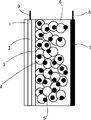
- FIG. 1 is a schematic diagram illustrating an example of a cross section perpendicular to the stacking direction of the structure of the photoelectric conversion element according to the present invention.
- FIG. 1 is an example of a schematic diagram illustrating a cross section orthogonal to the stacking direction of the photoelectric conversion element and the solar cell.
- the first electrode 2 is provided on the substrate 1
- the photosensitizing material 5 is adsorbed on the hole blocking layer 3
- the electron transport layer 4 and the electron transport layer made of titanium oxide
- the hole transport layer 6 is sandwiched between the second electrode 7.
- the first electrode 2 is not particularly limited as long as it is a conductive substance that is transparent to visible light, and a known one used for a normal photoelectric conversion element, a liquid crystal panel, or the like can be used.
- Examples of the material of the first electrode 2 include indium tin oxide (hereinafter referred to as ITO), fluorine-doped tin oxide (hereinafter referred to as FTO), antimony-doped tin oxide (hereinafter referred to as ATO), and indium.
- ITO indium tin oxide
- FTO fluorine-doped tin oxide
- ATO antimony-doped tin oxide
- -Zinc oxide, niobium / titanium oxide, graphene, etc. are mentioned. These may be used alone or in a plurality of layers.
- the thickness of the first electrode 2 is preferably 5 nm to 100 ⁇ m, more preferably 50 nm to 10 ⁇ m.
- the first electrode 2 is preferably provided on the substrate 1 made of a material transparent to visible light in order to maintain a certain hardness.
- the substrate 1 for example, glass, a transparent plastic plate, a transparent plastic film, an inorganic transparent crystal, or the like is used.
- FTO-coated glass ITO-coated glass
- zinc oxide aluminum-coated glass
- FTO-coated transparent plastic film ITO-coated transparent
- a plastic film etc. are mentioned.
- metal lead wire examples include metals such as aluminum, copper, silver, gold, platinum, and nickel.
- the metal lead wire can be formed by a method of installing the ITO or the FTO on the substrate 1 by vapor deposition, sputtering, pressure bonding, or the like.
- the hole blocking layer 3 is not particularly limited as long as it is transparent to visible light and has an electron transporting material, but titanium oxide is particularly preferable.
- titanium oxide is particularly preferable.
- the titanium oxide film is formed by a sol-gel method or a hydrolyzing method from titanium tetrachloride to form a wet film, but the resistance is low.
- a sputtering method for forming a dry film is more preferable.
- the hole blocking layer 3 is also formed for the purpose of preventing electronic contact between the first electrode 2 and the hole transport layer 6.
- the thickness of the hole blocking layer 3 is not particularly limited, but is preferably 5 nm to 1 ⁇ m, more preferably 500 nm to 700 nm for wet film formation, and more preferably 10 nm to 30 nm for dry film formation.
- the photoelectric conversion element and the solar cell of the present invention form the porous electron transport layer 4 on the hole blocking layer 3, and may be a single layer or a multilayer.
- the multi-layer it is possible to apply multi-layer coatings of semiconductor fine particle dispersions having different particle diameters, or to apply multi-layer coatings of different types of semiconductors, resins, and additives. When the thickness is insufficient with a single application, the multilayer application is an effective means.
- the thickness of the electron transport layer 4 is preferably 100 nm to 100 ⁇ m.
- the semiconductor is not particularly limited, and a known semiconductor can be used. Specifically, a single semiconductor such as silicon or germanium, a compound semiconductor typified by a metal chalcogenide, a compound having a perovskite structure, or the like can be given.
- the metal chalcogenides include titanium, tin, zinc, iron, tungsten, zirconium, hafnium, strontium, indium, cerium, yttrium, lanthanum, vanadium, niobium, or tantalum oxide, cadmium, zinc, lead, Silver, antimony, bismuth sulfide, cadmium, lead selenide, cadmium telluride and the like.
- Examples of other compound semiconductors include phosphides such as zinc, gallium, indium, cadmium, gallium arsenide, copper-indium-selenide, copper-indium-sulfide, and the like.
- Examples of the compound having a perovskite structure include strontium titanate, calcium titanate, sodium titanate, barium titanate, and potassium niobate. These may be used alone or in combination of two or more.
- an oxide semiconductor is preferable, and titanium oxide, zinc oxide, tin oxide, and niobium oxide are particularly preferable.
- the crystal type of these semiconductors is not particularly limited, and may be single crystal, polycrystal, or amorphous.
- the size of the semiconductor fine particles is not particularly limited, but the average primary particle size is preferably 1 nm to 100 nm, more preferably 5 nm to 50 nm.
- the efficiency can be improved by mixing or laminating semiconductor particles having a larger average particle diameter to scatter incident light.
- the average particle diameter of the semiconductor particles is preferably 50 nm to 500 nm.
- the method for producing the electron transport layer 4 is not particularly limited, and examples thereof include a method of forming a thin film in a vacuum such as sputtering and a wet film forming method.
- the wet film forming method is preferable, and a method in which a paste in which the semiconductor fine particle powder or sol is dispersed is prepared and applied to the electron collecting electrode substrate is more preferable.
- the coating method is not particularly limited and can be performed according to a known method, for example, a dip method, a spray method, a wire bar method, a spin coating method, a roller coating method, Examples thereof include a blade coating method and a gravure coating method.
- various methods such as a letterpress, an offset, a gravure, an intaglio, a rubber plate, screen printing, can be used, for example.
- the semiconductor fine particle dispersion is prepared by mechanical pulverization or using a mill, it is formed by dispersing at least semiconductor fine particles alone or a mixture of semiconductor fine particles and a resin in water or an organic solvent.
- the resin examples include polymers and copolymers of vinyl compounds such as styrene, vinyl acetate, acrylic acid ester, and methacrylic acid ester, silicon resin, phenoxy resin, polysulfone resin, polyvinyl butyral resin, polyvinyl formal resin, and polyester resin. , Cellulose ester resin, cellulose ether resin, urethane resin, phenol resin, epoxy resin, polycarbonate resin, polyarylate resin, polyamide resin, polyimide resin and the like.
- vinyl compounds such as styrene, vinyl acetate, acrylic acid ester, and methacrylic acid ester
- silicon resin phenoxy resin
- polysulfone resin polyvinyl butyral resin
- polyvinyl formal resin and polyester resin.
- Cellulose ester resin Cellulose ester resin, cellulose ether resin, urethane resin, phenol resin, epoxy resin, polycarbonate resin, polyarylate resin, polyamide resin, polyimide resin and the like.
- Examples of the solvent for dispersing the semiconductor fine particles include alcohol solvents such as water, methanol, ethanol, isopropyl alcohol, and ⁇ -terpineol, ketone solvents such as acetone, methyl ethyl ketone, and methyl isobutyl ketone, ethyl formate, ethyl acetate, Or ester solvents such as n-butyl acetate, ether solvents such as diethyl ether, dimethoxyethane, tetrahydrofuran, dioxolane, or dioxane, N, N-dimethylformamide, N, N-dimethylacetamide, or N-methyl-2- Amide solvents such as pyrrolidone, dichloromethane, chloroform, bromoform, methyl iodide, dichloroethane, trichloroethane, trichloroethylene, chlorobenzene, o-dichloro
- the semiconductor fine particle paste obtained by the dispersion of the semiconductor fine particles or the sol-gel method may be an acid such as hydrochloric acid, nitric acid or acetic acid, polyoxyethylene (10) octylphenyl ether.
- a surfactant such as acetylacetone, a chelating agent such as 2-aminoethanol, and ethylenediamine can be added.
- thickener for the purpose of improving the film forming property.
- the thickener include polymers such as polyethylene glycol and polyvinyl alcohol, and thickeners such as ethyl cellulose.
- the semiconductor fine particles may be subjected to firing, microwave irradiation, electron beam irradiation, or laser beam irradiation in order to bring the particles into electronic contact with each other after coating and to improve film strength and adhesion to the substrate. preferable. These processes may be performed alone or in combination of two or more.
- the range of the firing temperature is not particularly limited, but if the temperature is raised excessively, the resistance of the substrate may be increased or the substrate may be melted, and therefore 30 ° C. to 700 ° C. is preferable, and 100 ° C. to 600 ° C. ° C is more preferred.
- the firing time is not particularly limited, but is preferably 10 minutes to 10 hours.
- the microwave irradiation may be performed from the electron transport layer 4 formation side or from the back side. Although there is no restriction
- Electrochemical plating using a titanium trichloride aqueous solution may be performed.
- a film in which the semiconductor fine particles having a diameter of several tens of nanometers are laminated by sintering or the like forms a porous state.
- This nanoporous structure has a very high surface area, which can be expressed using a roughness factor.
- the roughness factor is a numerical value representing the actual area inside the porous with respect to the area of the semiconductor fine particles applied to the substrate. Therefore, the roughness factor is preferably as large as possible, but it is also related to the film thickness of the electron transport layer 4 and is preferably 20 or more in the present invention.
- the photosensitizing material is adsorbed on the surface of the electron transporting semiconductor that is the electron transporting layer 4.
- the photosensitizing material those represented by the general formula (2) are preferable.
- R 3 represents a substituted or unsubstituted alkyl group.
- Dye1 R 3 CH 2 CH 3 (Japanese scientific material dictionary number: J2.477.478C, J3.081.465G)
- Dye2 R 3 (CH 2 ) 3 CH 3
- Dye3 R 3 C (CH 3 ) 3
- Dye4 R 3 (CH 2 ) 9 CH 3
- Dye5 R 3 (CH 2 ) 2 COOH
- Dye6 R 3 (CH 2 ) 4 COOH
- Dye7 (CH 2 ) 7 COOH
- Dye8 R 3 (CH 2 ) 10 COOH (Japanese scientific substance dictionary number: J3.113.583D)
- the compound represented by the general formula (2) can be synthesized by the method described in Dye and Pigments 91 (2011) 145-152.
- the photosensitizing material 5 is not limited to the above as long as it is a compound that is photoexcited by the excitation light used, and specific examples thereof include the following compounds.
- JP-A-11-86916 JP-A-11-214730, JP-A-2000-106224, JP-A-2001-76773, JP-A-2003-7359. Described in JP-A-11-214731, JP-A-11-238905, JP-A-2001-52766, JP-A-2001-76775, JP-A-2003-7360, etc.
- Merocyanine dyes 9-arylxanthene compounds described in JP-A-10-92477, JP-A-11-273754, JP-A-11-273755, JP-A-2003-3173, etc., JP-A-10-93118 Triarylmethane compounds described in Japanese Patent Laid-Open No.
- the metal complex compound, the coumarin compound, the polyene compound, the indoline compound, and the thiophene compound are preferable.
- a method for adsorbing the photosensitizing material 5 to the electron transporting layer 4 a method of immersing an electron current collecting electrode containing semiconductor fine particles in a photosensitizing material solution or dispersion, a solution or dispersion is used as an electron transporting layer. It is possible to use a method of applying to and adsorbing to the surface.
- a method for immersing the electron current collecting electrode containing semiconductor fine particles in the photosensitizing material solution or dispersion for example, a dipping method, a dipping method, a roller method, an air knife method or the like can be used.
- a method for applying the solution or dispersion liquid to the electron transport layer and adsorbing it for example, a wire bar method, a slide hopper method, an extrusion method, a curtain method, a spin method, a spray method, or the like can be used. Further, it may be adsorbed in a supercritical fluid using carbon dioxide or the like.
- a condensing agent When adsorbing the photosensitizing material 5, a condensing agent may be used in combination.
- the condensing agent has a catalytic action that seems to physically or chemically bond the photosensitizing material and the electron transport compound to the inorganic surface, or acts stoichiometrically to move the chemical equilibrium advantageously. Any of those to be made may be used. Furthermore, you may add a thiol and a hydroxy compound as said condensation adjuvant.
- Examples of the solvent for dissolving or dispersing the photosensitizing material 5 include, for example, alcohol solvents such as water, methanol, ethanol, and isopropyl alcohol, ketone solvents such as acetone, methyl ethyl ketone, and methyl isobutyl ketone, ethyl formate, Ester solvents such as ethyl acetate or n-butyl acetate, ether solvents such as diethyl ether, dimethoxyethane, tetrahydrofuran, dioxolane, or dioxane, N, N-dimethylformamide, N, N-dimethylacetamide, or N-methyl Amide solvents such as -2-pyrrolidone, dichloromethane, chloroform, bromoform, methyl iodide, dichloroethane, trichloroethane, trichloroethylene, chlorobenzene, o-dich
- an aggregating and dissociating agent may be used in combination.
- the aggregating / dissociating agent is preferably a steroid compound such as cholic acid or chenodeoxycholic acid, a long-chain alkyl carboxylic acid or a long-chain alkyl phosphonic acid, and is appropriately selected according to the dye used.
- the addition amount of the aggregating and dissociating agent is preferably 0.01 to 500 parts by mass, more preferably 0.1 to 100 parts by mass with respect to 1 part by mass of the dye.
- the temperature at which the photosensitizing material is adsorbed alone or the temperature at which the photosensitizing material and the aggregating / dissociating agent are adsorbed is preferably ⁇ 50 ° C. or more and 200 ° C. or less. Moreover, this adsorption may be carried out while standing or stirring.
- the stirring method is not particularly limited and may be appropriately selected depending on the intended purpose. Examples thereof include a stirrer, a ball mill, a paint conditioner, a sand mill, an attritor, a disperser, and ultrasonic dispersion.
- the time required for the adsorption is preferably 5 seconds or more and 1000 hours or less, more preferably 10 seconds or more and 500 hours or less, and further preferably 1 minute or more and 150 hours.
- the adsorption is preferably performed in a dark place.
- the hole transport material 6 is not particularly limited as long as it contains at least one of an organic hole transport material and a basic compound represented by the general formula (1a) or the general formula (1b). It can be appropriately selected depending on the case.
- a general hole transport layer an electrolyte solution in which a redox couple is dissolved in an organic solvent, a gel electrolyte in which a liquid in which a redox couple is dissolved in an organic solvent is impregnated in a polymer matrix, and a molten salt containing the redox couple Solid electrolytes, inorganic hole transport materials, organic hole transport materials, and the like are used.
- Organic hole transport material can be used for either a single layered hole transporting layer 6 made of a single material or a stacked hole transporting layer 6 made of a plurality of compounds.
- the organic hole transport material used in the single layer structure made of the single material a known organic hole transport compound is used. Specific examples thereof include oxadiazole compounds disclosed in JP-B No. 34-5466, triphenylmethane compounds disclosed in JP-B No. 45-555, JP-B No. 52-4188, and the like. Pyrazoline compounds shown, hydrazone compounds shown in JP-B-55-42380, etc., oxadiazole compounds shown in JP-A-56-123544, etc., JP-A-54-58445 Tetraarylbenzidine compounds shown in JP-A-58-65440 or JP-A-60-98437, Adv. Mater. , 813, vol. 17, spirobifluorene compounds such as spiro-OMeTAD described in (2005).
- the hole transport material called spiro-OMeTAD is preferable in that it exhibits excellent photoelectric conversion characteristics.
- a known hole transport polymer material is used as the polymer material used for the hole transport layer 6 close to the second electrode 7 used in the laminated structure.
- a known hole transport polymer material includes poly (3-n-hexylthiophene), poly (3-n-octyloxythiophene), poly (9,9′-dioctyl-fluorene-co-bithiophene), poly (3,3 ′′ '-Didodecyl-quarterthiophene), poly (3,6-dioctylthieno [3,2-b] thiophene), poly (2,5-bis (3-decylthiophen-2-yl) thieno [3,2-b Thiophene), poly (3,4-didecylthiophene-co-thieno [3,2-b] thiophene), poly (3,6-dioctylthieno [3,2-b] thiophene-co-thieno [3, 2-b]
- additives may be added to the organic hole transport material.
- the additive include iodine, lithium iodide, sodium iodide, potassium iodide, cesium iodide, calcium iodide, copper iodide, iron iodide, silver iodide and other metal iodides, Quaternary ammonium salts such as tetraalkylammonium iodide, pyridinium iodide, metal bromides such as lithium bromide, sodium bromide, potassium bromide, cesium bromide, calcium bromide, Bromine salts of quaternary ammonium compounds such as tetraalkylammonium bromide and pyridinium bromide, Metal chlorides such as copper chloride and silver chloride, metal acetates such as copper acetate, silver acetate and palladium acetate, Metal sulfates such as copper sulfate and zinc sulf
- a particularly high open-circuit voltage can be obtained by adding a basic compound represented by the following general formula (1a) or general formula (1b) to the organic hole transport material. Further, the internal resistance of the photoelectric conversion element is increased, and the loss current in weak light such as room light can be reduced. Therefore, an open circuit voltage higher than that of a conventional basic compound can be obtained.
- R 1, R 2 represents a substituted or unsubstituted alkyl group or an aromatic hydrocarbon group, may be the same or different. Also, R 1, R 2 are each And may form a substituted or unsubstituted heterocyclic group containing a nitrogen atom, and examples of the substituent include an alkyl group, an aromatic hydrocarbon group, and a substituted or unsubstituted alkoxy group.
- the hole transport layer 6 uses the organic hole transport material and is different from the hole transport model using the iodine electrolyte solution or the like. Therefore, the amount of decrease in the short-circuit current density is small, and a high open circuit voltage can be obtained, whereby excellent photoelectric conversion characteristics can be obtained. Furthermore, when photoelectric conversion was performed in weak light such as room light, which is rarely reported, it was verified that a particularly significant advantage appears.
- the addition amount of the basic compound represented by the general formula (1a) or the general formula (1b) in the hole transport layer 6 is 1 part by mass or more and 20 parts by mass or less with respect to 100 parts by mass of the organic hole transport material. It is preferable that it is 5 mass parts or more and 15 mass parts or less.
- R 1 and R 2 represent a substituted or unsubstituted alkyl group or an aromatic hydrocarbon group, and may be the same or different. In addition, R 1 and R 2 may be mutually different. And a substituted or unsubstituted heterocyclic group containing a nitrogen atom may be formed, and X represents a halogen element.
- the oxidizing agent for making a part of said organic hole transport material into a radical cation for the purpose of improving electroconductivity.
- the oxidizing agent include tris (4-bromophenyl) aminium hexachloroantimonate, silver hexafluoroantimonate, nitrosonium tetrafluorate, silver nitrate, and cobalt complex compounds.
- the added oxidizing agent may or may not be taken out of the system after the addition.
- the hole transport layer 6 is formed directly on the electron transport layer 4 carrying the photosensitizing material.
- the method of forming a thin film in vacuum, such as vacuum deposition, and the wet film forming method are mentioned. In consideration of production cost and the like, the wet film forming method is particularly preferable, and a method of coating on the electron transport layer 4 is preferable.
- the application method is not particularly limited and can be performed according to a known method, for example, a dip method, a spray method, a wire bar method, a spin coating method, a roller coating method, Examples thereof include a blade coating method and a gravure coating method.
- a wet printing method various methods, such as a letterpress, an offset, a gravure, an intaglio, a rubber plate, screen printing, can be used, for example.
- the film may be formed in a supercritical fluid or a subcritical fluid having a temperature and pressure lower than the critical point.
- the supercritical fluid exists as a non-aggregating high-density fluid in a temperature / pressure region that exceeds the limit (critical point) at which gas and liquid can coexist, and does not aggregate even when compressed.
- the fluid is not particularly limited as long as it is in the above state, and can be appropriately selected according to the purpose. However, a fluid having a low critical temperature is preferable.
- the supercritical fluid examples include carbon monoxide, carbon dioxide, ammonia, nitrogen, water, ercol solvents such as methanol, ethanol, n-butanol, ethane, propane, 2,3-dimethylbutane, benzene, toluene, and the like.
- ercol solvents such as methanol, ethanol, n-butanol, ethane, propane, 2,3-dimethylbutane, benzene, toluene, and the like.
- hydrocarbon solvents halogen solvents such as methylene chloride and chlorotrifluoromethane
- ether solvents such as dimethyl ether.
- the carbon dioxide since the carbon dioxide has a critical pressure of 7.3 MPa and a critical temperature of 31 ° C., it is particularly preferable because it can easily create a supercritical state and is nonflammable and easy to handle.
- these fluids may be one kind alone or a mixture of two or more kinds.
- the subcritical fluid is not particularly limited as long as it exists as a high pressure liquid in a temperature and pressure region near the critical point, and can be appropriately selected according to the purpose.
- the compounds mentioned as the supercritical fluid can also be suitably used as the subcritical fluid.
- the critical temperature and critical pressure of the supercritical fluid are not particularly limited and may be appropriately selected depending on the intended purpose.
- the critical temperature is preferably ⁇ 273 ° C. or higher and 300 ° C. or lower, preferably 0 ° C. or higher and 200 ° C. or lower. Is particularly preferred.
- an organic solvent or an entrainer can be used in combination. By adding the organic solvent and the entrainer, the solubility in the supercritical fluid can be easily adjusted.
- the organic solvent is not particularly limited and may be appropriately selected depending on the intended purpose.
- examples thereof include ketone solvents such as acetone, methyl ethyl ketone, and methyl isobutyl ketone, and esters such as ethyl formate, ethyl acetate, and n-butyl acetate.
- Solvents such as diisopropyl ether, dimethoxyethane, tetrahydrofuran, dioxolane, dioxane, amide solvents such as N, N-dimethylformamide, N, N-dimethylacetamide, N-methyl-2-pyrrolidone, dichloromethane, chloroform Halogenated hydrocarbons such as bromoform, methyl iodide, dichloroethane, trichloroethane, trichloroethylene, chlorobenzene, o-dichlorobenzene, fluorobenzene, bromobenzene, iodobenzene, 1-chloronaphthalene Carbonization of medium, n-pentane, n-hexane, n-octane, 1,5-hexadiene, cyclohexane, methylcyclohexane, cyclohexadiene, benzene
- the press treatment step may be performed after the organic hole transport material is provided on the first electrode 2 provided with the electron transport material coated with the photosensitizing material.
- the press processing method is not particularly limited, and examples thereof include a press molding method using a flat plate represented by an IR tablet shaper, and a roll press method using a roller.
- the pressure in the press treatment is preferably 10 kgf / cm 2 or more, more preferably 30 kgf / cm 2 or more. Although there is no restriction
- a release material may be sandwiched between the press and the electrode.
- the release material include polytetrafluoroethylene, polychlorotrifluoride ethylene, tetrafluoroethylene hexafluoropropylene copolymer, perfluoroalkoxy fluoride resin, polyvinylidene fluoride, and ethylene tetrafluoride ethylene copolymer.
- fluororesins such as ethylene chlorotrifluoride ethylene copolymer and polyvinyl fluoride.
- a metal oxide may be provided between the organic hole transport material and the second electrode 7.
- the metal oxide include molybdenum oxide, tungsten oxide, vanadium oxide, nickel oxide, and the like. Among these, the molybdenum oxide is particularly preferable.
- the hole transport layer 6 may have a single layer structure made of a single material or a laminated structure made of a plurality of compounds.
- the laminated structure it is preferable to use a polymer material for the organic hole transport material layer close to the second electrode 7.
- the surface of the porous electron transport layer 4 can be further smoothed and the photoelectric conversion characteristics can be improved by using the polymer material having excellent film forming properties. Moreover, since it is difficult for the polymer material to penetrate into the porous electron transport layer 4, it is excellent in covering the surface of the porous electron transport layer 4. Therefore, higher performance can be obtained.
- the method for providing the metal oxide on the organic hole transport material is not particularly limited, and examples thereof include a method of forming a thin film in a vacuum such as sputtering or vacuum deposition, a wet film forming method, and the like.
- the wet film forming method is preferably a method in which a paste in which the metal oxide powder or sol is dispersed is prepared and applied onto the hole transport layer 6.
- the coating method is not particularly limited and can be performed according to a known method, for example, a dipping method, a spray method, a wire bar method, a spin coating method, a roller coating method, a blade coating method. Method, gravure coating method and the like. Various methods such as letterpress, offset, gravure, intaglio, rubber plate, and screen printing can be used as the wet printing method.
- the thickness of the second electrode is preferably 0.1 nm to 50 nm, and more preferably 1 nm to 10 nm.
- the second electrode 7 is newly applied after the hole transport layer 6 is formed or on the metal oxide.
- the second electrode 7 can be usually the same as the first electrode 2 described above, and a support is not necessarily required in a configuration in which strength and sealability are sufficiently maintained.
- Examples of the material of the second electrode 7 include metals such as platinum, gold, silver, copper, and aluminum, carbon compounds such as graphite, fullerene, carbon nanotube, and graphene, and conductive metal oxides such as ITO, FTO, and ATO. And conductive polymers such as polythiophene and polyaniline.
- the first electrode 2 and the second electrode 7 In order to operate as a dye-sensitized solar cell, at least one of the first electrode 2 and the second electrode 7 must be substantially transparent.
- a method in which the first electrode 2 side is transparent and sunlight is incident from the first electrode 2 side is preferable.
- a material that reflects light is preferably used on the second electrode 7 side, and a metal, glass, plastic, or metal thin film on which a conductive oxide is deposited is preferable. It is also effective to provide an antireflection layer on the sunlight incident side.
- the dye-sensitized solar cell of the present invention can be applied to a power supply device using a solar cell.
- any device can be used as long as it has conventionally used a solar cell or a power supply device using the solar cell.
- examples of utilizing the characteristics of the photoelectric conversion element of the present invention include a power supply device provided in a mobile phone, an electronic notebook, electronic paper, and the like. It can also be used as an auxiliary power source for extending the continuous use time of a rechargeable or dry battery type electric appliance.
- Example 1 (Production of titanium oxide semiconductor electrode) Mixing 2 ml of titanium tetra-n-propoxide, 4 ml of acetic acid, 1 ml of ion-exchanged water, and 40 ml of 2-propanol, spin-coating on an FTO glass substrate, drying at room temperature, baking in air at 450 ° C. for 30 minutes, A titanium oxide semiconductor electrode was produced. Using the same solution again, it was applied by spin coating on the obtained electrode so as to have a film thickness of 100 nm, and baked in air at 450 ° C. for 30 minutes to form a hole blocking layer.
- the titanium oxide semiconductor electrode is immersed in the Dye8 (0.5 mM, acetonitrile / t-butanol (volume ratio 1: 1) solution) as a sensitizing dye, and left to stand in a dark place for 1 hour to obtain a photosensitizing material. Adsorbed.
- Dye8 0.5 mM, acetonitrile / t-butanol (volume ratio 1: 1) solution
- an organic hole transport material (Merck Co., Ltd., brand: 2,2 ′, 7,7′-tetrakis (N, N-di-p-methoxyphenylamino) -9,9 '-Spirobifluorene, product number: SHT-263) dissolved in chlorobenzene (solid content: 14% by mass), lithium bis (trifluoromethanesulfonyl) imide (solid content: 1% by mass) manufactured by Kanto Chemical Co., Ltd., and exemplified basic compound No .
- a hole transport layer was formed by spin coating of a solution obtained by adding 1 (solid content of 1.4% by mass) on a semiconductor electrode carrying a photosensitizer. On this, silver was vacuum-deposited to a thickness of 100 nm to prepare a dye-sensitized solar cell.
- Example 2 The basic compound in Example 1 was exemplified by Compound No. A photoelectric conversion device was prepared and evaluated in the same manner as in Example 1 except that the basic compound was changed to 3. The results are shown in Tables 2 and 3.
- Example 3 The basic compound in Example 1 was exemplified by Compound No. A photoelectric conversion element was prepared and evaluated in the same manner as in Example 1 except that the basic compound was changed to 5 (basic compound). The results are shown in Tables 2 and 3.
- Example 4 The basic compound in Example 1 was exemplified by Compound No. A photoelectric conversion device was prepared and evaluated in the same manner as in Example 1 except that the basic compound was changed to 8. The results are shown in Tables 2 and 3.
- Example 5 The basic compound in Example 1 was exemplified by Compound No. A photoelectric conversion device was prepared and evaluated in the same manner as in Example 1 except that the basic compound was changed to 10. The results are shown in Tables 2 and 3.
- Example 6 The basic compound in Example 1 was exemplified by Compound No. A photoelectric conversion element was produced and evaluated in the same manner as in Example 1 except that the basic compound was changed to 12. The results are shown in Tables 2 and 3.
- Example 7 The dye in Example 1 is the dye of Dye1, the basic compound is Exemplified Compound No. A photoelectric conversion element was produced and evaluated in the same manner as in Example 1 except that the basic compound was changed to 13. The results are shown in Tables 2 and 3.
- Example 8 The dye in Example 1 is the dye of Dye1, the basic compound is Exemplified Compound No. A photoelectric conversion device was prepared and evaluated in the same manner as in Example 1 except that the basic compound was changed to 15 basic compounds. The results are shown in Tables 2 and 3.
- Example 9 The dye in Example 1 is the dye of Dye1, the basic compound is Exemplified Compound No. A photoelectric conversion element was produced and evaluated in the same manner as in Example 1 except that the basic compound was changed to 16 basic compounds. The results are shown in Tables 2 and 3.
- Example 10 The dye in Example 1 is the dye of Dye4, the basic compound is Exemplified Compound No. A photoelectric conversion device was prepared and evaluated in the same manner as in Example 1 except that the basic compound was changed to 18. The results are shown in Tables 2 and 3.
- Example 11 The dye in Example 1 is the dye of Dye4, the basic compound is Exemplified Compound No. A photoelectric conversion element was prepared and evaluated in the same manner as in Example 1 except that the basic compound was changed to 20 basic compounds. The results are shown in Tables 2 and 3.
- Example 12 The dye in Example 1 is the dye of Dye4, the basic compound is Exemplified Compound No. A photoelectric conversion element was produced and evaluated in the same manner as in Example 1 except that the basic compound was changed to 13. The results are shown in Tables 2 and 3.
- Example 13 The dye in Example 1 is the dye of Dye8, the basic compound is Exemplified Compound No. A photoelectric conversion element was produced and evaluated in the same manner as in Example 1 except that the basic compound was changed to 13. The results are shown in Tables 2 and 3.
- Example 14 In the same manner as in Example 1, except that lithium bis (trifluoromethanesulfonyl) imide in Example 1 was changed to 1-n-hexyl-3-methylimidazolinium bis (trifluoromethylsulfonyl) imide. Sensitive solar cells were prepared and evaluated. The results are shown in Tables 2 and 3.
- Example 15 A dye-sensitized solar cell was prepared and evaluated in the same manner as in Example 1 except that the following hole transport layer was inserted between the hole transport layer and the silver electrode in Example 1. The results are shown in Tables 2 and 3.
- a solution obtained by adding 1-n-hexyl-3-methylimidazolinium trifluorosulfonyldiimide (27 mM) to chlorobenzene (solid content 2 mass%) in which poly (3-n-hexylthiophene) manufactured by Aldrich is dissolved was spray-coated on the hole transport layer to form a film of about 100 nm.
- Example 16 The dye in Example 1 is the dye of Dye8, the basic compound is Exemplified Compound No. A photoelectric conversion element was produced and evaluated in the same manner as in Example 1 except that the basic compound was changed to 21. The results are shown in Tables 2 and 3.
- Example 17 The basic compound in Example 1 was exemplified by Compound No. A photoelectric conversion device was prepared and evaluated in the same manner as in Example 1 except that the basic compound was changed to 23. The results are shown in Tables 2 and 3.
- Example 18 The basic compound in Example 1 was exemplified by Compound No. A photoelectric conversion element was produced and evaluated in the same manner as in Example 1 except that the basic compound was changed to 24. The results are shown in Tables 2 and 3.
- Example 19 The basic compound in Example 1 was exemplified by Compound No. A photoelectric conversion device was prepared and evaluated in the same manner as in Example 1 except that the basic compound was changed to 26. The results are shown in Tables 2 and 3.
- Example 20 The basic compound in Example 1 was exemplified by Compound No. A photoelectric conversion device was prepared and evaluated in the same manner as in Example 1 except that the basic compound was changed to 28. The results are shown in Tables 2 and 3.
- Example 21 The basic compound in Example 1 was exemplified by Compound No. A photoelectric conversion device was prepared and evaluated in the same manner as in Example 1 except that the basic compound was changed to 29. The results are shown in Tables 2 and 3.
- Example 22 The dye in Example 1 is the dye of Dye1, the basic compound is Exemplified Compound No. A photoelectric conversion device was prepared and evaluated in the same manner as in Example 1 except that the basic compound was changed to 26. The results are shown in Tables 2 and 3.
- Example 23 The dye in Example 1 is the dye of Dye1, the basic compound is Exemplified Compound No. A photoelectric conversion device was prepared and evaluated in the same manner as in Example 1 except that the basic compound was changed to 30. The results are shown in Tables 2 and 3.
- Example 24 The dye in Example 1 is the dye of Dye1, the basic compound is Exemplified Compound No. A photoelectric conversion element was produced and evaluated in the same manner as in Example 1 except that the basic compound was changed to 31. The results are shown in Tables 2 and 3.
- Example 25 The dye in Example 1 is the dye of Dye4, the basic compound is Exemplified Compound No. A photoelectric conversion element was produced and evaluated in the same manner as in Example 1 except that the basic compound was changed to 21. The results are shown in Tables 2 and 3.
- Example 26 The dye in Example 1 is the dye of Dye4, the basic compound is Exemplified Compound No. A photoelectric conversion device was prepared and evaluated in the same manner as in Example 1 except that the basic compound was changed to 26. The results are shown in Tables 2 and 3.
- Example 27 The dye in Example 1 is the dye of Dye4, the basic compound is Exemplified Compound No. A photoelectric conversion device was prepared and evaluated in the same manner as in Example 1 except that the basic compound was changed to 28. The results are shown in Tables 2 and 3.
- Example 28 In the same manner as in Example 1, except that lithium bis (trifluoromethanesulfonyl) imide in Example 1 was changed to 1-n-hexyl-3-methylimidazolinium bis (trifluoromethylsulfonyl) imide. Sensitive solar cells were prepared and evaluated. The results are shown in Tables 2 and 3.
- Example 29 A dye-sensitized solar cell was prepared and evaluated in the same manner as in Example 16 except that the following hole transport layer was inserted between the hole transport layer and the silver electrode in Example 16. The results are shown in Tables 2 and 3.
- a solution obtained by adding 1-n-hexyl-3-methylimidazolinium trifluorosulfonyldiimide (27 mM) to chlorobenzene (solid content 2 mass%) in which poly (3-n-hexylthiophene) manufactured by Aldrich is dissolved was spray-coated on the hole transport layer to form a film of about 100 nm.
- Example 1 A photoelectric conversion device was prepared and evaluated in the same manner as in Example 1 except that the basic compound in Example 1 was changed to tarbutyl pyridine manufactured by Aldrich. The results are shown in Tables 2 and 3.
- the dye-sensitized solar cell of the present invention exhibits excellent photoelectric conversion characteristics.
- a photoelectric conversion element having a first electrode, a hole blocking layer, an electron transport layer, a first hole transport layer, and a second electrode Said 1st hole transport layer is a photoelectric conversion element characterized by including at least 1 among the basic compounds represented by the following general formula (1a) and general formula (1b).
- R 1 and R 2 represent a substituted or unsubstituted alkyl group or an aromatic hydrocarbon group, which may be the same or different, and R 1 and R 2 are And may be bonded to form a substituted or unsubstituted heterocyclic group containing a nitrogen atom.
- the electron transporting layer includes an electron transporting material photosensitized with a photosensitizing material represented by the following general formula (2).
- R 3 represents a substituted or unsubstituted alkyl group.
- the electron transporting material is at least one selected from titanium oxide, zinc oxide, tin oxide, and niobium oxide.
- the hole blocking layer includes titanium oxide.
- the first hole transport layer includes an ionic liquid.
- the ionic liquid includes an imidazolium compound.
- ⁇ 7> Any one of ⁇ 1> to ⁇ 6>, further including a second hole transport layer including a hole transporting polymer material between the first hole transport layer and the second electrode. It is a photoelectric conversion element as described in an item.
- a solar cell comprising the photoelectric conversion element according to any one of ⁇ 1> to ⁇ 7>.
- the first electrode, a hole blocking layer, an electron transport layer, a first hole transport layer, and a second electrode are provided.
- One hole transport layer uses at least one of the basic materials represented by the general formula (1a) or the general formula (1b), thereby increasing the internal resistance and the open circuit voltage. It is possible to obtain a solar cell with good characteristics in room light.
Landscapes
- Engineering & Computer Science (AREA)
- Chemical & Material Sciences (AREA)
- Power Engineering (AREA)
- Materials Engineering (AREA)
- Physics & Mathematics (AREA)
- Spectroscopy & Molecular Physics (AREA)
- Microelectronics & Electronic Packaging (AREA)
- Inorganic Chemistry (AREA)
- Electromagnetism (AREA)
- Manufacturing & Machinery (AREA)
- Electrochemistry (AREA)
- Chemical Kinetics & Catalysis (AREA)
- Photovoltaic Devices (AREA)
- Hybrid Cells (AREA)
- Electroluminescent Light Sources (AREA)
Priority Applications (8)
| Application Number | Priority Date | Filing Date | Title |
|---|---|---|---|
| JP2016504016A JP6520914B2 (ja) | 2014-02-24 | 2015-01-30 | 固体型光電変換素子及び太陽電池 |
| KR1020207013591A KR20200056470A (ko) | 2014-02-24 | 2015-01-30 | 광전 변환 소자 및 태양 전지 |
| CN201580010108.1A CN106062985A (zh) | 2014-02-24 | 2015-01-30 | 光电转换元件和太阳能电池 |
| KR1020167025653A KR102112330B1 (ko) | 2014-02-24 | 2015-01-30 | 광전 변환 소자 및 태양 전지 |
| EP15752787.0A EP3113240B1 (en) | 2014-02-24 | 2015-01-30 | Photoelectric conversion element and solar cell |
| US15/120,464 US10636579B2 (en) | 2014-02-24 | 2015-01-30 | Photoelectric conversion element and solar cell |
| KR1020217017859A KR102330122B1 (ko) | 2014-02-24 | 2015-01-30 | 광전 변환 소자 및 태양 전지 |
| US16/829,356 US11101080B2 (en) | 2014-02-24 | 2020-03-25 | Photoelectric conversion element and solar cell |
Applications Claiming Priority (4)
| Application Number | Priority Date | Filing Date | Title |
|---|---|---|---|
| JP2014032566 | 2014-02-24 | ||
| JP2014-032566 | 2014-02-24 | ||
| JP2014-084832 | 2014-04-16 | ||
| JP2014084832 | 2014-04-16 |
Related Child Applications (2)
| Application Number | Title | Priority Date | Filing Date |
|---|---|---|---|
| US15/120,464 A-371-Of-International US10636579B2 (en) | 2014-02-24 | 2015-01-30 | Photoelectric conversion element and solar cell |
| US16/829,356 Continuation US11101080B2 (en) | 2014-02-24 | 2020-03-25 | Photoelectric conversion element and solar cell |
Publications (1)
| Publication Number | Publication Date |
|---|---|
| WO2015125587A1 true WO2015125587A1 (ja) | 2015-08-27 |
Family
ID=53878099
Family Applications (1)
| Application Number | Title | Priority Date | Filing Date |
|---|---|---|---|
| PCT/JP2015/052684 Ceased WO2015125587A1 (ja) | 2014-02-24 | 2015-01-30 | 光電変換素子及び太陽電池 |
Country Status (6)
| Country | Link |
|---|---|
| US (2) | US10636579B2 (enExample) |
| EP (1) | EP3113240B1 (enExample) |
| JP (3) | JP6520914B2 (enExample) |
| KR (3) | KR102112330B1 (enExample) |
| CN (2) | CN110690350A (enExample) |
| WO (1) | WO2015125587A1 (enExample) |
Cited By (16)
| Publication number | Priority date | Publication date | Assignee | Title |
|---|---|---|---|---|
| JP2017098372A (ja) * | 2015-11-20 | 2017-06-01 | 株式会社リコー | 光電変換素子及び太陽電池 |
| WO2017130820A1 (ja) * | 2016-01-25 | 2017-08-03 | 株式会社リコー | 光電変換素子 |
| JP2017139376A (ja) * | 2016-02-04 | 2017-08-10 | 株式会社リコー | 光電変換素子 |
| JP2017212368A (ja) * | 2016-05-26 | 2017-11-30 | 株式会社リコー | ホール輸送材料及び、光電変換素子並びに太陽電池 |
| JP2017212364A (ja) * | 2016-05-26 | 2017-11-30 | 株式会社リコー | ホール輸送材料及び、光電変換素子並びに太陽電池 |
| JP2017222640A (ja) * | 2016-06-08 | 2017-12-21 | 株式会社リコー | 3級アミン化合物、光電変換素子、及び太陽電池 |
| JP2018006622A (ja) * | 2016-07-05 | 2018-01-11 | 株式会社リコー | 光電変換素子及び太陽電池 |
| JP2018113305A (ja) * | 2017-01-10 | 2018-07-19 | 株式会社リコー | 光電変換素子及び太陽電池 |
| US10367103B2 (en) | 2015-05-08 | 2019-07-30 | Ricoh Company, Ltd. | Photoelectric conversion element |
| JP2019176136A (ja) * | 2018-03-29 | 2019-10-10 | 株式会社リコー | 光電変換素子、及び光電変換素子モジュール |
| JP2020074416A (ja) * | 2019-12-26 | 2020-05-14 | 株式会社リコー | 光電変換素子、太陽電池及び合成方法 |
| JP2020102602A (ja) * | 2018-03-19 | 2020-07-02 | 株式会社リコー | 光電変換素子、及び光電変換素子モジュール |
| US10727001B2 (en) | 2014-04-16 | 2020-07-28 | Ricoh Company, Ltd. | Photoelectric conversion element |
| JP2021027078A (ja) * | 2019-07-31 | 2021-02-22 | 株式会社リコー | 光電変換素子、電子機器、及び電源モジュール |
| US11056600B2 (en) | 2018-03-30 | 2021-07-06 | Ricoh Company, Ltd. | Photoelectric conversion element, photoelectric conversion element module, electronic device, and power supply module |
| JP2022078536A (ja) * | 2020-11-13 | 2022-05-25 | 株式会社リコー | 光電変換素子、光電変換モジュール、電子機器、及び電源モジュール |
Families Citing this family (17)
| Publication number | Priority date | Publication date | Assignee | Title |
|---|---|---|---|---|
| KR102163405B1 (ko) | 2016-12-07 | 2020-10-08 | 가부시키가이샤 리코 | 광전 변환 소자 |
| US10319533B2 (en) | 2017-01-12 | 2019-06-11 | Ricoh Company, Ltd. | Photoelectric conversion element and solar cell |
| WO2019181701A1 (en) * | 2018-03-19 | 2019-09-26 | Ricoh Company, Ltd. | Photoelectric conversion element and photoelectric conversion element module |
| JP2019165073A (ja) | 2018-03-19 | 2019-09-26 | 株式会社リコー | 太陽電池モジュール |
| KR20200131293A (ko) | 2018-03-19 | 2020-11-23 | 가부시키가이샤 리코 | 광전 변환 디바이스, 프로세스 카트리지 및 화상 형성 장치 |
| KR102093431B1 (ko) * | 2018-09-13 | 2020-03-25 | 경북대학교 산학협력단 | 페로브스카이트 태양전지 및 이의 제조방법 |
| WO2020107978A1 (zh) * | 2018-11-29 | 2020-06-04 | Tcl科技集团股份有限公司 | 量子点发光二极管及其制备方法 |
| JP2020127007A (ja) * | 2019-02-01 | 2020-08-20 | 株式会社リコー | 光電変換素子、太陽電池モジュール、電源モジュール、及び電子機器 |
| CN114127975B (zh) | 2019-07-16 | 2025-08-12 | 株式会社理光 | 太阳能电池模块、电子装置和电源模块 |
| WO2021107158A1 (en) | 2019-11-28 | 2021-06-03 | Ricoh Company, Ltd. | Photoelectric conversion element, photoelectric conversion module, electronic device, and power supply module |
| US20210167287A1 (en) * | 2019-11-28 | 2021-06-03 | Tamotsu Horiuchi | Photoelectric conversion element, photoelectric conversion module, electronic device, and power supply module |
| JP7413833B2 (ja) | 2020-02-27 | 2024-01-16 | 株式会社リコー | 光電変換素子及び光電変換モジュール |
| US11502264B2 (en) | 2020-02-27 | 2022-11-15 | Ricoh Company, Ltd. | Photoelectric conversion element and photoelectric conversion module |
| JP7651842B2 (ja) * | 2020-11-13 | 2025-03-27 | 株式会社リコー | 光電変換素子、光電変換モジュール、電子機器、及び電源モジュール |
| EP4092704B1 (en) * | 2021-05-20 | 2025-07-09 | Ricoh Company, Ltd. | Photoelectric conversion element and method for producing photoelectric conversion element, photoelectric conversion module, and electronic device |
| CN115915793A (zh) * | 2021-09-30 | 2023-04-04 | 株式会社理光 | 光电转换元件、光电转换模块及电子设备 |
| WO2023107547A2 (en) * | 2021-12-08 | 2023-06-15 | Kineta, Inc. | Azetidine and spiroazetidine compounds and uses thereof |
Citations (4)
| Publication number | Priority date | Publication date | Assignee | Title |
|---|---|---|---|---|
| JP2004047229A (ja) * | 2002-07-10 | 2004-02-12 | National Institute Of Advanced Industrial & Technology | アミノピリジン系化合物を含む電解質溶液を用いた光電変換素子及びそれを用いた色素増感型太陽電池 |
| JP2011181286A (ja) * | 2010-02-26 | 2011-09-15 | Tdk Corp | 色素増感型太陽電池 |
| CN102290257A (zh) * | 2011-05-19 | 2011-12-21 | 内蒙古大学 | 一种可选择性透光的染料敏化太阳能电池的制备方法 |
| JP2013109965A (ja) * | 2011-11-21 | 2013-06-06 | Konica Minolta Business Technologies Inc | 光電変換素子およびこれを含む太陽電池 |
Family Cites Families (21)
| Publication number | Priority date | Publication date | Assignee | Title |
|---|---|---|---|---|
| CH674596A5 (enExample) | 1988-02-12 | 1990-06-15 | Sulzer Ag | |
| JPH1144773A (ja) | 1997-07-25 | 1999-02-16 | Citizen Watch Co Ltd | 外部操作切り換え構造 |
| JPH11144773A (ja) | 1997-09-05 | 1999-05-28 | Fuji Photo Film Co Ltd | 光電変換素子および光再生型光電気化学電池 |
| JP2000106223A (ja) | 1998-09-29 | 2000-04-11 | Fuji Photo Film Co Ltd | 光電変換素子 |
| EP1456861B1 (en) * | 2001-12-21 | 2011-10-05 | Sony Deutschland GmbH | A polymer gel hybrid solar cell |
| EP2006949A2 (en) | 2006-03-02 | 2008-12-24 | Tokyo University of Science, Educational Foundation | Method for producing photoelectrode for dye-sensitized solar cell, photoelectrode for dye-sensitized solar cell, and dye-sensitized solar cell |
| US8158880B1 (en) * | 2007-01-17 | 2012-04-17 | Aqt Solar, Inc. | Thin-film photovoltaic structures including semiconductor grain and oxide layers |
| KR20110129959A (ko) * | 2009-03-17 | 2011-12-02 | 코나르카 테크놀로지, 인코포레이티드 | 염료 감응형 전지용 금속 기판 |
| US8664518B2 (en) * | 2009-12-11 | 2014-03-04 | Konica Minolta Holdngs, Inc. | Organic photoelectric conversion element and producing method of the same |
| JP5700937B2 (ja) * | 2010-02-09 | 2015-04-15 | 保土谷化学工業株式会社 | 光電変換用増感色素及びそれを用いた光電変換素子及び色素増感太陽電池 |
| GB201004106D0 (en) * | 2010-03-11 | 2010-04-28 | Isis Innovation | Device |
| KR101537654B1 (ko) | 2010-04-22 | 2015-07-17 | 히타치가세이가부시끼가이샤 | 유기 일렉트로닉스 재료, 중합 개시제 및 열중합 개시제, 잉크 조성물, 유기 박막 및 그 제조 방법, 유기 일렉트로닉스 소자, 유기 일렉트로 루미네센스 소자, 조명 장치, 표시 소자, 및 표시 장치 |
| WO2012051337A2 (en) * | 2010-10-12 | 2012-04-19 | The Regents Of The University Of Michigan | Photoactive devices including porphyrinoids coordinating additives |
| US20120177813A1 (en) * | 2010-10-17 | 2012-07-12 | Thompson Mark E | Chemical annealing method for fabrication of organic thin films for optoelectronic devices |
| JP2012113942A (ja) * | 2010-11-24 | 2012-06-14 | Ricoh Co Ltd | 多層型光電変換素子およびその製造方法 |
| JP2012199023A (ja) * | 2011-03-18 | 2012-10-18 | Ricoh Co Ltd | 光電変換素子及びその製造方法 |
| JP5629625B2 (ja) | 2011-03-28 | 2014-11-26 | 株式会社豊田中央研究所 | 色素増感型太陽電池の製造方法、色素増感型太陽電池及び色素増感型太陽電池モジュール |
| KR101354638B1 (ko) * | 2011-06-20 | 2014-01-22 | 제일모직주식회사 | 유기광전자소자용 재료, 이를 포함하는 유기발광소자 및 상기 유기발광소자를 포함하는 표시장치 |
| KR20130005918A (ko) * | 2011-07-08 | 2013-01-16 | 주식회사 세원 | 염료감응 태양전지용 겔형 전해질 |
| PL2850627T3 (pl) * | 2012-05-18 | 2016-10-31 | Urządzenie optoelektroniczne zawierające porowaty materiał rusztowania oraz perowskity | |
| JP6194614B2 (ja) | 2012-12-18 | 2017-09-13 | 株式会社リコー | 光電変換素子 |
-
2015
- 2015-01-30 KR KR1020167025653A patent/KR102112330B1/ko active Active
- 2015-01-30 KR KR1020207013591A patent/KR20200056470A/ko not_active Ceased
- 2015-01-30 US US15/120,464 patent/US10636579B2/en active Active
- 2015-01-30 EP EP15752787.0A patent/EP3113240B1/en active Active
- 2015-01-30 KR KR1020217017859A patent/KR102330122B1/ko active Active
- 2015-01-30 JP JP2016504016A patent/JP6520914B2/ja active Active
- 2015-01-30 WO PCT/JP2015/052684 patent/WO2015125587A1/ja not_active Ceased
- 2015-01-30 CN CN201911069220.9A patent/CN110690350A/zh active Pending
- 2015-01-30 CN CN201580010108.1A patent/CN106062985A/zh active Pending
-
2018
- 2018-12-28 JP JP2018246911A patent/JP2019083324A/ja active Pending
-
2020
- 2020-03-25 US US16/829,356 patent/US11101080B2/en active Active
- 2020-09-16 JP JP2020155165A patent/JP2021005723A/ja active Pending
Patent Citations (4)
| Publication number | Priority date | Publication date | Assignee | Title |
|---|---|---|---|---|
| JP2004047229A (ja) * | 2002-07-10 | 2004-02-12 | National Institute Of Advanced Industrial & Technology | アミノピリジン系化合物を含む電解質溶液を用いた光電変換素子及びそれを用いた色素増感型太陽電池 |
| JP2011181286A (ja) * | 2010-02-26 | 2011-09-15 | Tdk Corp | 色素増感型太陽電池 |
| CN102290257A (zh) * | 2011-05-19 | 2011-12-21 | 内蒙古大学 | 一种可选择性透光的染料敏化太阳能电池的制备方法 |
| JP2013109965A (ja) * | 2011-11-21 | 2013-06-06 | Konica Minolta Business Technologies Inc | 光電変換素子およびこれを含む太陽電池 |
Non-Patent Citations (2)
| Title |
|---|
| H. KUSAMA ET AL.: "Influence of alkylaminopyridine additives in electrolytes on dye-sensitized solar cell performance", SOLAR ENERGY MATERIALS AND SOLAR CELLS, vol. 81, no. 1, 2004, pages 87 - 99, XP004482764 * |
| See also references of EP3113240A4 * |
Cited By (21)
| Publication number | Priority date | Publication date | Assignee | Title |
|---|---|---|---|---|
| US11069485B2 (en) | 2014-04-16 | 2021-07-20 | Ricoh Company, Ltd. | Photoelectric conversion element |
| US10727001B2 (en) | 2014-04-16 | 2020-07-28 | Ricoh Company, Ltd. | Photoelectric conversion element |
| US10367103B2 (en) | 2015-05-08 | 2019-07-30 | Ricoh Company, Ltd. | Photoelectric conversion element |
| JP2017098372A (ja) * | 2015-11-20 | 2017-06-01 | 株式会社リコー | 光電変換素子及び太陽電池 |
| JPWO2017130820A1 (ja) * | 2016-01-25 | 2018-12-06 | 株式会社リコー | 光電変換素子 |
| WO2017130820A1 (ja) * | 2016-01-25 | 2017-08-03 | 株式会社リコー | 光電変換素子 |
| US10763050B2 (en) | 2016-01-25 | 2020-09-01 | Ricoh Company, Ltd. | Photoelectric conversion element |
| JP2017139376A (ja) * | 2016-02-04 | 2017-08-10 | 株式会社リコー | 光電変換素子 |
| JP2017212368A (ja) * | 2016-05-26 | 2017-11-30 | 株式会社リコー | ホール輸送材料及び、光電変換素子並びに太陽電池 |
| JP2017212364A (ja) * | 2016-05-26 | 2017-11-30 | 株式会社リコー | ホール輸送材料及び、光電変換素子並びに太陽電池 |
| JP2017222640A (ja) * | 2016-06-08 | 2017-12-21 | 株式会社リコー | 3級アミン化合物、光電変換素子、及び太陽電池 |
| JP2018006622A (ja) * | 2016-07-05 | 2018-01-11 | 株式会社リコー | 光電変換素子及び太陽電池 |
| JP2018113305A (ja) * | 2017-01-10 | 2018-07-19 | 株式会社リコー | 光電変換素子及び太陽電池 |
| US11081662B2 (en) * | 2017-01-10 | 2021-08-03 | Ricoh Company, Ltd. | Photoelectric conversion element and solar cell |
| JP2020102602A (ja) * | 2018-03-19 | 2020-07-02 | 株式会社リコー | 光電変換素子、及び光電変換素子モジュール |
| JP2019176136A (ja) * | 2018-03-29 | 2019-10-10 | 株式会社リコー | 光電変換素子、及び光電変換素子モジュール |
| US11056600B2 (en) | 2018-03-30 | 2021-07-06 | Ricoh Company, Ltd. | Photoelectric conversion element, photoelectric conversion element module, electronic device, and power supply module |
| JP2021027078A (ja) * | 2019-07-31 | 2021-02-22 | 株式会社リコー | 光電変換素子、電子機器、及び電源モジュール |
| JP2020074416A (ja) * | 2019-12-26 | 2020-05-14 | 株式会社リコー | 光電変換素子、太陽電池及び合成方法 |
| JP7003387B2 (ja) | 2019-12-26 | 2022-01-20 | 株式会社リコー | 光電変換素子、太陽電池及び合成方法 |
| JP2022078536A (ja) * | 2020-11-13 | 2022-05-25 | 株式会社リコー | 光電変換素子、光電変換モジュール、電子機器、及び電源モジュール |
Also Published As
| Publication number | Publication date |
|---|---|
| US20200273630A1 (en) | 2020-08-27 |
| JP2021005723A (ja) | 2021-01-14 |
| JP6520914B2 (ja) | 2019-05-29 |
| CN110690350A (zh) | 2020-01-14 |
| KR20160124186A (ko) | 2016-10-26 |
| US20170069431A1 (en) | 2017-03-09 |
| KR102112330B1 (ko) | 2020-05-19 |
| US11101080B2 (en) | 2021-08-24 |
| KR20200056470A (ko) | 2020-05-22 |
| JPWO2015125587A1 (ja) | 2017-03-30 |
| US10636579B2 (en) | 2020-04-28 |
| CN106062985A (zh) | 2016-10-26 |
| KR102330122B1 (ko) | 2021-11-24 |
| KR20210073610A (ko) | 2021-06-18 |
| JP2019083324A (ja) | 2019-05-30 |
| EP3113240B1 (en) | 2024-04-03 |
| EP3113240A4 (en) | 2017-03-15 |
| EP3113240A1 (en) | 2017-01-04 |
Similar Documents
| Publication | Publication Date | Title |
|---|---|---|
| JP6520914B2 (ja) | 固体型光電変換素子及び太陽電池 | |
| JP6249093B2 (ja) | 光電変換素子 | |
| JP6555344B2 (ja) | 光電変換素子 | |
| JP6447754B2 (ja) | 光電変換素子 | |
| JP6405689B2 (ja) | 光電変換素子及び太陽電池 | |
| JP6340758B2 (ja) | 光電変換素子の製造方法 | |
| JP6579480B2 (ja) | 光電変換素子及び二次電池 | |
| JP2011065751A (ja) | 光電変換素子 | |
| JP2018006622A (ja) | 光電変換素子及び太陽電池 | |
| JP2013211149A (ja) | 光電変換素子およびその製造方法 | |
| JP6111552B2 (ja) | 光電変換素子、及び光電変換素子の製造方法 | |
| JP6641599B2 (ja) | ホール輸送材料及び、光電変換素子並びに太陽電池 | |
| JP2017222640A (ja) | 3級アミン化合物、光電変換素子、及び太陽電池 | |
| JP6657841B2 (ja) | 光電変換素子及び太陽電池 | |
| JP6740621B2 (ja) | 光電変換素子 | |
| JP2017011066A (ja) | 光電変換素子 | |
| JP2020074416A (ja) | 光電変換素子、太陽電池及び合成方法 | |
| JP6899083B2 (ja) | 光電変換素子及び二次電池 | |
| JP6677078B2 (ja) | ホール輸送材料及び、光電変換素子並びに太陽電池 |
Legal Events
| Date | Code | Title | Description |
|---|---|---|---|
| 121 | Ep: the epo has been informed by wipo that ep was designated in this application |
Ref document number: 15752787 Country of ref document: EP Kind code of ref document: A1 |
|
| ENP | Entry into the national phase |
Ref document number: 2016504016 Country of ref document: JP Kind code of ref document: A |
|
| WWE | Wipo information: entry into national phase |
Ref document number: 15120464 Country of ref document: US |
|
| REEP | Request for entry into the european phase |
Ref document number: 2015752787 Country of ref document: EP |
|
| WWE | Wipo information: entry into national phase |
Ref document number: 2015752787 Country of ref document: EP |
|
| NENP | Non-entry into the national phase |
Ref country code: DE |
|
| ENP | Entry into the national phase |
Ref document number: 20167025653 Country of ref document: KR Kind code of ref document: A |