WO2015125205A1 - Procédé de fabrication de dispositif à semi-conducteurs et dispositif à semi-conducteurs - Google Patents
Procédé de fabrication de dispositif à semi-conducteurs et dispositif à semi-conducteurs Download PDFInfo
- Publication number
- WO2015125205A1 WO2015125205A1 PCT/JP2014/053746 JP2014053746W WO2015125205A1 WO 2015125205 A1 WO2015125205 A1 WO 2015125205A1 JP 2014053746 W JP2014053746 W JP 2014053746W WO 2015125205 A1 WO2015125205 A1 WO 2015125205A1
- Authority
- WO
- WIPO (PCT)
- Prior art keywords
- insulating film
- semiconductor layer
- gate
- metal
- forming
- Prior art date
Links
- 239000004065 semiconductor Substances 0.000 title claims abstract description 233
- 238000004519 manufacturing process Methods 0.000 title claims abstract description 65
- 229910052751 metal Inorganic materials 0.000 claims abstract description 97
- 239000002184 metal Substances 0.000 claims abstract description 97
- 229910021420 polycrystalline silicon Inorganic materials 0.000 claims abstract description 57
- 229920005591 polysilicon Polymers 0.000 claims abstract description 55
- 238000009792 diffusion process Methods 0.000 claims abstract description 25
- 239000000758 substrate Substances 0.000 claims abstract description 16
- 239000010410 layer Substances 0.000 claims description 205
- 238000005530 etching Methods 0.000 claims description 27
- 238000000151 deposition Methods 0.000 claims description 17
- 150000001875 compounds Chemical class 0.000 claims description 12
- 239000011229 interlayer Substances 0.000 claims description 12
- 238000000034 method Methods 0.000 abstract description 21
- XUIMIQQOPSSXEZ-UHFFFAOYSA-N Silicon Chemical compound [Si] XUIMIQQOPSSXEZ-UHFFFAOYSA-N 0.000 description 56
- 229910052710 silicon Inorganic materials 0.000 description 56
- 239000010703 silicon Substances 0.000 description 56
- 150000004767 nitrides Chemical class 0.000 description 6
- 239000012535 impurity Substances 0.000 description 4
- 230000003071 parasitic effect Effects 0.000 description 3
- 238000005498 polishing Methods 0.000 description 3
- 239000000126 substance Substances 0.000 description 3
- ZOXJGFHDIHLPTG-UHFFFAOYSA-N Boron Chemical compound [B] ZOXJGFHDIHLPTG-UHFFFAOYSA-N 0.000 description 1
- OAICVXFJPJFONN-UHFFFAOYSA-N Phosphorus Chemical compound [P] OAICVXFJPJFONN-UHFFFAOYSA-N 0.000 description 1
- 229910052785 arsenic Inorganic materials 0.000 description 1
- RQNWIZPPADIBDY-UHFFFAOYSA-N arsenic atom Chemical compound [As] RQNWIZPPADIBDY-UHFFFAOYSA-N 0.000 description 1
- 230000015572 biosynthetic process Effects 0.000 description 1
- 229910052796 boron Inorganic materials 0.000 description 1
- 238000005229 chemical vapour deposition Methods 0.000 description 1
- 230000010354 integration Effects 0.000 description 1
- 238000004518 low pressure chemical vapour deposition Methods 0.000 description 1
- 239000000463 material Substances 0.000 description 1
- 238000012986 modification Methods 0.000 description 1
- 230000004048 modification Effects 0.000 description 1
- 229910052698 phosphorus Inorganic materials 0.000 description 1
- 239000011574 phosphorus Substances 0.000 description 1
Images


Classifications
-
- H—ELECTRICITY
- H01—ELECTRIC ELEMENTS
- H01L—SEMICONDUCTOR DEVICES NOT COVERED BY CLASS H10
- H01L29/00—Semiconductor devices specially adapted for rectifying, amplifying, oscillating or switching and having potential barriers; Capacitors or resistors having potential barriers, e.g. a PN-junction depletion layer or carrier concentration layer; Details of semiconductor bodies or of electrodes thereof ; Multistep manufacturing processes therefor
- H01L29/40—Electrodes ; Multistep manufacturing processes therefor
- H01L29/43—Electrodes ; Multistep manufacturing processes therefor characterised by the materials of which they are formed
- H01L29/49—Metal-insulator-semiconductor electrodes, e.g. gates of MOSFET
- H01L29/4966—Metal-insulator-semiconductor electrodes, e.g. gates of MOSFET the conductor material next to the insulator being a composite material, e.g. organic material, TiN, MoSi2
-
- H—ELECTRICITY
- H01—ELECTRIC ELEMENTS
- H01L—SEMICONDUCTOR DEVICES NOT COVERED BY CLASS H10
- H01L21/00—Processes or apparatus adapted for the manufacture or treatment of semiconductor or solid state devices or of parts thereof
- H01L21/70—Manufacture or treatment of devices consisting of a plurality of solid state components formed in or on a common substrate or of parts thereof; Manufacture of integrated circuit devices or of parts thereof
- H01L21/77—Manufacture or treatment of devices consisting of a plurality of solid state components or integrated circuits formed in, or on, a common substrate
- H01L21/78—Manufacture or treatment of devices consisting of a plurality of solid state components or integrated circuits formed in, or on, a common substrate with subsequent division of the substrate into plural individual devices
- H01L21/82—Manufacture or treatment of devices consisting of a plurality of solid state components or integrated circuits formed in, or on, a common substrate with subsequent division of the substrate into plural individual devices to produce devices, e.g. integrated circuits, each consisting of a plurality of components
- H01L21/822—Manufacture or treatment of devices consisting of a plurality of solid state components or integrated circuits formed in, or on, a common substrate with subsequent division of the substrate into plural individual devices to produce devices, e.g. integrated circuits, each consisting of a plurality of components the substrate being a semiconductor, using silicon technology
- H01L21/8232—Field-effect technology
- H01L21/8234—MIS technology, i.e. integration processes of field effect transistors of the conductor-insulator-semiconductor type
- H01L21/823431—MIS technology, i.e. integration processes of field effect transistors of the conductor-insulator-semiconductor type with a particular manufacturing method of transistors with a horizontal current flow in a vertical sidewall of a semiconductor body, e.g. FinFET, MuGFET
-
- H—ELECTRICITY
- H01—ELECTRIC ELEMENTS
- H01L—SEMICONDUCTOR DEVICES NOT COVERED BY CLASS H10
- H01L21/00—Processes or apparatus adapted for the manufacture or treatment of semiconductor or solid state devices or of parts thereof
- H01L21/70—Manufacture or treatment of devices consisting of a plurality of solid state components formed in or on a common substrate or of parts thereof; Manufacture of integrated circuit devices or of parts thereof
- H01L21/77—Manufacture or treatment of devices consisting of a plurality of solid state components or integrated circuits formed in, or on, a common substrate
- H01L21/78—Manufacture or treatment of devices consisting of a plurality of solid state components or integrated circuits formed in, or on, a common substrate with subsequent division of the substrate into plural individual devices
- H01L21/82—Manufacture or treatment of devices consisting of a plurality of solid state components or integrated circuits formed in, or on, a common substrate with subsequent division of the substrate into plural individual devices to produce devices, e.g. integrated circuits, each consisting of a plurality of components
- H01L21/822—Manufacture or treatment of devices consisting of a plurality of solid state components or integrated circuits formed in, or on, a common substrate with subsequent division of the substrate into plural individual devices to produce devices, e.g. integrated circuits, each consisting of a plurality of components the substrate being a semiconductor, using silicon technology
- H01L21/8232—Field-effect technology
- H01L21/8234—MIS technology, i.e. integration processes of field effect transistors of the conductor-insulator-semiconductor type
- H01L21/823487—MIS technology, i.e. integration processes of field effect transistors of the conductor-insulator-semiconductor type with a particular manufacturing method of vertical transistor structures, i.e. with channel vertical to the substrate surface
-
- H—ELECTRICITY
- H01—ELECTRIC ELEMENTS
- H01L—SEMICONDUCTOR DEVICES NOT COVERED BY CLASS H10
- H01L21/00—Processes or apparatus adapted for the manufacture or treatment of semiconductor or solid state devices or of parts thereof
- H01L21/70—Manufacture or treatment of devices consisting of a plurality of solid state components formed in or on a common substrate or of parts thereof; Manufacture of integrated circuit devices or of parts thereof
- H01L21/77—Manufacture or treatment of devices consisting of a plurality of solid state components or integrated circuits formed in, or on, a common substrate
- H01L21/78—Manufacture or treatment of devices consisting of a plurality of solid state components or integrated circuits formed in, or on, a common substrate with subsequent division of the substrate into plural individual devices
- H01L21/82—Manufacture or treatment of devices consisting of a plurality of solid state components or integrated circuits formed in, or on, a common substrate with subsequent division of the substrate into plural individual devices to produce devices, e.g. integrated circuits, each consisting of a plurality of components
- H01L21/822—Manufacture or treatment of devices consisting of a plurality of solid state components or integrated circuits formed in, or on, a common substrate with subsequent division of the substrate into plural individual devices to produce devices, e.g. integrated circuits, each consisting of a plurality of components the substrate being a semiconductor, using silicon technology
- H01L21/8232—Field-effect technology
- H01L21/8234—MIS technology, i.e. integration processes of field effect transistors of the conductor-insulator-semiconductor type
- H01L21/8238—Complementary field-effect transistors, e.g. CMOS
- H01L21/823821—Complementary field-effect transistors, e.g. CMOS with a particular manufacturing method of transistors with a horizontal current flow in a vertical sidewall of a semiconductor body, e.g. FinFET, MuGFET
-
- H—ELECTRICITY
- H01—ELECTRIC ELEMENTS
- H01L—SEMICONDUCTOR DEVICES NOT COVERED BY CLASS H10
- H01L27/00—Devices consisting of a plurality of semiconductor or other solid-state components formed in or on a common substrate
- H01L27/02—Devices consisting of a plurality of semiconductor or other solid-state components formed in or on a common substrate including semiconductor components specially adapted for rectifying, oscillating, amplifying or switching and having potential barriers; including integrated passive circuit elements having potential barriers
- H01L27/04—Devices consisting of a plurality of semiconductor or other solid-state components formed in or on a common substrate including semiconductor components specially adapted for rectifying, oscillating, amplifying or switching and having potential barriers; including integrated passive circuit elements having potential barriers the substrate being a semiconductor body
- H01L27/08—Devices consisting of a plurality of semiconductor or other solid-state components formed in or on a common substrate including semiconductor components specially adapted for rectifying, oscillating, amplifying or switching and having potential barriers; including integrated passive circuit elements having potential barriers the substrate being a semiconductor body including only semiconductor components of a single kind
- H01L27/085—Devices consisting of a plurality of semiconductor or other solid-state components formed in or on a common substrate including semiconductor components specially adapted for rectifying, oscillating, amplifying or switching and having potential barriers; including integrated passive circuit elements having potential barriers the substrate being a semiconductor body including only semiconductor components of a single kind including field-effect components only
- H01L27/088—Devices consisting of a plurality of semiconductor or other solid-state components formed in or on a common substrate including semiconductor components specially adapted for rectifying, oscillating, amplifying or switching and having potential barriers; including integrated passive circuit elements having potential barriers the substrate being a semiconductor body including only semiconductor components of a single kind including field-effect components only the components being field-effect transistors with insulated gate
- H01L27/0886—Devices consisting of a plurality of semiconductor or other solid-state components formed in or on a common substrate including semiconductor components specially adapted for rectifying, oscillating, amplifying or switching and having potential barriers; including integrated passive circuit elements having potential barriers the substrate being a semiconductor body including only semiconductor components of a single kind including field-effect components only the components being field-effect transistors with insulated gate including transistors with a horizontal current flow in a vertical sidewall of a semiconductor body, e.g. FinFET, MuGFET
-
- H—ELECTRICITY
- H01—ELECTRIC ELEMENTS
- H01L—SEMICONDUCTOR DEVICES NOT COVERED BY CLASS H10
- H01L27/00—Devices consisting of a plurality of semiconductor or other solid-state components formed in or on a common substrate
- H01L27/02—Devices consisting of a plurality of semiconductor or other solid-state components formed in or on a common substrate including semiconductor components specially adapted for rectifying, oscillating, amplifying or switching and having potential barriers; including integrated passive circuit elements having potential barriers
- H01L27/04—Devices consisting of a plurality of semiconductor or other solid-state components formed in or on a common substrate including semiconductor components specially adapted for rectifying, oscillating, amplifying or switching and having potential barriers; including integrated passive circuit elements having potential barriers the substrate being a semiconductor body
- H01L27/08—Devices consisting of a plurality of semiconductor or other solid-state components formed in or on a common substrate including semiconductor components specially adapted for rectifying, oscillating, amplifying or switching and having potential barriers; including integrated passive circuit elements having potential barriers the substrate being a semiconductor body including only semiconductor components of a single kind
- H01L27/085—Devices consisting of a plurality of semiconductor or other solid-state components formed in or on a common substrate including semiconductor components specially adapted for rectifying, oscillating, amplifying or switching and having potential barriers; including integrated passive circuit elements having potential barriers the substrate being a semiconductor body including only semiconductor components of a single kind including field-effect components only
- H01L27/088—Devices consisting of a plurality of semiconductor or other solid-state components formed in or on a common substrate including semiconductor components specially adapted for rectifying, oscillating, amplifying or switching and having potential barriers; including integrated passive circuit elements having potential barriers the substrate being a semiconductor body including only semiconductor components of a single kind including field-effect components only the components being field-effect transistors with insulated gate
- H01L27/092—Devices consisting of a plurality of semiconductor or other solid-state components formed in or on a common substrate including semiconductor components specially adapted for rectifying, oscillating, amplifying or switching and having potential barriers; including integrated passive circuit elements having potential barriers the substrate being a semiconductor body including only semiconductor components of a single kind including field-effect components only the components being field-effect transistors with insulated gate complementary MIS field-effect transistors
- H01L27/0924—Devices consisting of a plurality of semiconductor or other solid-state components formed in or on a common substrate including semiconductor components specially adapted for rectifying, oscillating, amplifying or switching and having potential barriers; including integrated passive circuit elements having potential barriers the substrate being a semiconductor body including only semiconductor components of a single kind including field-effect components only the components being field-effect transistors with insulated gate complementary MIS field-effect transistors including transistors with a horizontal current flow in a vertical sidewall of a semiconductor body, e.g. FinFET, MuGFET
-
- H—ELECTRICITY
- H01—ELECTRIC ELEMENTS
- H01L—SEMICONDUCTOR DEVICES NOT COVERED BY CLASS H10
- H01L29/00—Semiconductor devices specially adapted for rectifying, amplifying, oscillating or switching and having potential barriers; Capacitors or resistors having potential barriers, e.g. a PN-junction depletion layer or carrier concentration layer; Details of semiconductor bodies or of electrodes thereof ; Multistep manufacturing processes therefor
- H01L29/02—Semiconductor bodies ; Multistep manufacturing processes therefor
- H01L29/06—Semiconductor bodies ; Multistep manufacturing processes therefor characterised by their shape; characterised by the shapes, relative sizes, or dispositions of the semiconductor regions ; characterised by the concentration or distribution of impurities within semiconductor regions
- H01L29/0657—Semiconductor bodies ; Multistep manufacturing processes therefor characterised by their shape; characterised by the shapes, relative sizes, or dispositions of the semiconductor regions ; characterised by the concentration or distribution of impurities within semiconductor regions characterised by the shape of the body
- H01L29/0665—Semiconductor bodies ; Multistep manufacturing processes therefor characterised by their shape; characterised by the shapes, relative sizes, or dispositions of the semiconductor regions ; characterised by the concentration or distribution of impurities within semiconductor regions characterised by the shape of the body the shape of the body defining a nanostructure
- H01L29/0669—Nanowires or nanotubes
- H01L29/0676—Nanowires or nanotubes oriented perpendicular or at an angle to a substrate
-
- H—ELECTRICITY
- H01—ELECTRIC ELEMENTS
- H01L—SEMICONDUCTOR DEVICES NOT COVERED BY CLASS H10
- H01L29/00—Semiconductor devices specially adapted for rectifying, amplifying, oscillating or switching and having potential barriers; Capacitors or resistors having potential barriers, e.g. a PN-junction depletion layer or carrier concentration layer; Details of semiconductor bodies or of electrodes thereof ; Multistep manufacturing processes therefor
- H01L29/40—Electrodes ; Multistep manufacturing processes therefor
- H01L29/41—Electrodes ; Multistep manufacturing processes therefor characterised by their shape, relative sizes or dispositions
- H01L29/417—Electrodes ; Multistep manufacturing processes therefor characterised by their shape, relative sizes or dispositions carrying the current to be rectified, amplified or switched
- H01L29/41725—Source or drain electrodes for field effect devices
- H01L29/41791—Source or drain electrodes for field effect devices for transistors with a horizontal current flow in a vertical sidewall, e.g. FinFET, MuGFET
-
- H—ELECTRICITY
- H01—ELECTRIC ELEMENTS
- H01L—SEMICONDUCTOR DEVICES NOT COVERED BY CLASS H10
- H01L29/00—Semiconductor devices specially adapted for rectifying, amplifying, oscillating or switching and having potential barriers; Capacitors or resistors having potential barriers, e.g. a PN-junction depletion layer or carrier concentration layer; Details of semiconductor bodies or of electrodes thereof ; Multistep manufacturing processes therefor
- H01L29/40—Electrodes ; Multistep manufacturing processes therefor
- H01L29/41—Electrodes ; Multistep manufacturing processes therefor characterised by their shape, relative sizes or dispositions
- H01L29/423—Electrodes ; Multistep manufacturing processes therefor characterised by their shape, relative sizes or dispositions not carrying the current to be rectified, amplified or switched
- H01L29/42312—Gate electrodes for field effect devices
- H01L29/42316—Gate electrodes for field effect devices for field-effect transistors
- H01L29/4232—Gate electrodes for field effect devices for field-effect transistors with insulated gate
- H01L29/42384—Gate electrodes for field effect devices for field-effect transistors with insulated gate for thin film field effect transistors, e.g. characterised by the thickness or the shape of the insulator or the dimensions, the shape or the lay-out of the conductor
- H01L29/42392—Gate electrodes for field effect devices for field-effect transistors with insulated gate for thin film field effect transistors, e.g. characterised by the thickness or the shape of the insulator or the dimensions, the shape or the lay-out of the conductor fully surrounding the channel, e.g. gate-all-around
-
- H—ELECTRICITY
- H01—ELECTRIC ELEMENTS
- H01L—SEMICONDUCTOR DEVICES NOT COVERED BY CLASS H10
- H01L29/00—Semiconductor devices specially adapted for rectifying, amplifying, oscillating or switching and having potential barriers; Capacitors or resistors having potential barriers, e.g. a PN-junction depletion layer or carrier concentration layer; Details of semiconductor bodies or of electrodes thereof ; Multistep manufacturing processes therefor
- H01L29/66—Types of semiconductor device ; Multistep manufacturing processes therefor
- H01L29/66007—Multistep manufacturing processes
- H01L29/66075—Multistep manufacturing processes of devices having semiconductor bodies comprising group 14 or group 13/15 materials
- H01L29/66227—Multistep manufacturing processes of devices having semiconductor bodies comprising group 14 or group 13/15 materials the devices being controllable only by the electric current supplied or the electric potential applied, to an electrode which does not carry the current to be rectified, amplified or switched, e.g. three-terminal devices
- H01L29/66409—Unipolar field-effect transistors
- H01L29/66477—Unipolar field-effect transistors with an insulated gate, i.e. MISFET
- H01L29/66545—Unipolar field-effect transistors with an insulated gate, i.e. MISFET using a dummy, i.e. replacement gate in a process wherein at least a part of the final gate is self aligned to the dummy gate
-
- H—ELECTRICITY
- H01—ELECTRIC ELEMENTS
- H01L—SEMICONDUCTOR DEVICES NOT COVERED BY CLASS H10
- H01L29/00—Semiconductor devices specially adapted for rectifying, amplifying, oscillating or switching and having potential barriers; Capacitors or resistors having potential barriers, e.g. a PN-junction depletion layer or carrier concentration layer; Details of semiconductor bodies or of electrodes thereof ; Multistep manufacturing processes therefor
- H01L29/66—Types of semiconductor device ; Multistep manufacturing processes therefor
- H01L29/66007—Multistep manufacturing processes
- H01L29/66075—Multistep manufacturing processes of devices having semiconductor bodies comprising group 14 or group 13/15 materials
- H01L29/66227—Multistep manufacturing processes of devices having semiconductor bodies comprising group 14 or group 13/15 materials the devices being controllable only by the electric current supplied or the electric potential applied, to an electrode which does not carry the current to be rectified, amplified or switched, e.g. three-terminal devices
- H01L29/66409—Unipolar field-effect transistors
- H01L29/66477—Unipolar field-effect transistors with an insulated gate, i.e. MISFET
- H01L29/66666—Vertical transistors
-
- H—ELECTRICITY
- H01—ELECTRIC ELEMENTS
- H01L—SEMICONDUCTOR DEVICES NOT COVERED BY CLASS H10
- H01L29/00—Semiconductor devices specially adapted for rectifying, amplifying, oscillating or switching and having potential barriers; Capacitors or resistors having potential barriers, e.g. a PN-junction depletion layer or carrier concentration layer; Details of semiconductor bodies or of electrodes thereof ; Multistep manufacturing processes therefor
- H01L29/66—Types of semiconductor device ; Multistep manufacturing processes therefor
- H01L29/66007—Multistep manufacturing processes
- H01L29/66075—Multistep manufacturing processes of devices having semiconductor bodies comprising group 14 or group 13/15 materials
- H01L29/66227—Multistep manufacturing processes of devices having semiconductor bodies comprising group 14 or group 13/15 materials the devices being controllable only by the electric current supplied or the electric potential applied, to an electrode which does not carry the current to be rectified, amplified or switched, e.g. three-terminal devices
- H01L29/66409—Unipolar field-effect transistors
- H01L29/66477—Unipolar field-effect transistors with an insulated gate, i.e. MISFET
- H01L29/66742—Thin film unipolar transistors
- H01L29/66772—Monocristalline silicon transistors on insulating substrates, e.g. quartz substrates
-
- H—ELECTRICITY
- H01—ELECTRIC ELEMENTS
- H01L—SEMICONDUCTOR DEVICES NOT COVERED BY CLASS H10
- H01L29/00—Semiconductor devices specially adapted for rectifying, amplifying, oscillating or switching and having potential barriers; Capacitors or resistors having potential barriers, e.g. a PN-junction depletion layer or carrier concentration layer; Details of semiconductor bodies or of electrodes thereof ; Multistep manufacturing processes therefor
- H01L29/66—Types of semiconductor device ; Multistep manufacturing processes therefor
- H01L29/66007—Multistep manufacturing processes
- H01L29/66075—Multistep manufacturing processes of devices having semiconductor bodies comprising group 14 or group 13/15 materials
- H01L29/66227—Multistep manufacturing processes of devices having semiconductor bodies comprising group 14 or group 13/15 materials the devices being controllable only by the electric current supplied or the electric potential applied, to an electrode which does not carry the current to be rectified, amplified or switched, e.g. three-terminal devices
- H01L29/66409—Unipolar field-effect transistors
- H01L29/66477—Unipolar field-effect transistors with an insulated gate, i.e. MISFET
- H01L29/66787—Unipolar field-effect transistors with an insulated gate, i.e. MISFET with a gate at the side of the channel
- H01L29/66795—Unipolar field-effect transistors with an insulated gate, i.e. MISFET with a gate at the side of the channel with a horizontal current flow in a vertical sidewall of a semiconductor body, e.g. FinFET, MuGFET
-
- H—ELECTRICITY
- H01—ELECTRIC ELEMENTS
- H01L—SEMICONDUCTOR DEVICES NOT COVERED BY CLASS H10
- H01L29/00—Semiconductor devices specially adapted for rectifying, amplifying, oscillating or switching and having potential barriers; Capacitors or resistors having potential barriers, e.g. a PN-junction depletion layer or carrier concentration layer; Details of semiconductor bodies or of electrodes thereof ; Multistep manufacturing processes therefor
- H01L29/66—Types of semiconductor device ; Multistep manufacturing processes therefor
- H01L29/68—Types of semiconductor device ; Multistep manufacturing processes therefor controllable by only the electric current supplied, or only the electric potential applied, to an electrode which does not carry the current to be rectified, amplified or switched
- H01L29/76—Unipolar devices, e.g. field effect transistors
- H01L29/772—Field effect transistors
- H01L29/78—Field effect transistors with field effect produced by an insulated gate
- H01L29/785—Field effect transistors with field effect produced by an insulated gate having a channel with a horizontal current flow in a vertical sidewall of a semiconductor body, e.g. FinFET, MuGFET
-
- H—ELECTRICITY
- H01—ELECTRIC ELEMENTS
- H01L—SEMICONDUCTOR DEVICES NOT COVERED BY CLASS H10
- H01L29/00—Semiconductor devices specially adapted for rectifying, amplifying, oscillating or switching and having potential barriers; Capacitors or resistors having potential barriers, e.g. a PN-junction depletion layer or carrier concentration layer; Details of semiconductor bodies or of electrodes thereof ; Multistep manufacturing processes therefor
- H01L29/66—Types of semiconductor device ; Multistep manufacturing processes therefor
- H01L29/68—Types of semiconductor device ; Multistep manufacturing processes therefor controllable by only the electric current supplied, or only the electric potential applied, to an electrode which does not carry the current to be rectified, amplified or switched
- H01L29/76—Unipolar devices, e.g. field effect transistors
- H01L29/772—Field effect transistors
- H01L29/78—Field effect transistors with field effect produced by an insulated gate
- H01L29/786—Thin film transistors, i.e. transistors with a channel being at least partly a thin film
- H01L29/78642—Vertical transistors
-
- H—ELECTRICITY
- H01—ELECTRIC ELEMENTS
- H01L—SEMICONDUCTOR DEVICES NOT COVERED BY CLASS H10
- H01L29/00—Semiconductor devices specially adapted for rectifying, amplifying, oscillating or switching and having potential barriers; Capacitors or resistors having potential barriers, e.g. a PN-junction depletion layer or carrier concentration layer; Details of semiconductor bodies or of electrodes thereof ; Multistep manufacturing processes therefor
- H01L29/66—Types of semiconductor device ; Multistep manufacturing processes therefor
- H01L29/68—Types of semiconductor device ; Multistep manufacturing processes therefor controllable by only the electric current supplied, or only the electric potential applied, to an electrode which does not carry the current to be rectified, amplified or switched
- H01L29/76—Unipolar devices, e.g. field effect transistors
- H01L29/772—Field effect transistors
- H01L29/78—Field effect transistors with field effect produced by an insulated gate
- H01L29/786—Thin film transistors, i.e. transistors with a channel being at least partly a thin film
- H01L29/78651—Silicon transistors
- H01L29/78654—Monocrystalline silicon transistors
-
- H—ELECTRICITY
- H01—ELECTRIC ELEMENTS
- H01L—SEMICONDUCTOR DEVICES NOT COVERED BY CLASS H10
- H01L29/00—Semiconductor devices specially adapted for rectifying, amplifying, oscillating or switching and having potential barriers; Capacitors or resistors having potential barriers, e.g. a PN-junction depletion layer or carrier concentration layer; Details of semiconductor bodies or of electrodes thereof ; Multistep manufacturing processes therefor
- H01L29/66—Types of semiconductor device ; Multistep manufacturing processes therefor
- H01L29/68—Types of semiconductor device ; Multistep manufacturing processes therefor controllable by only the electric current supplied, or only the electric potential applied, to an electrode which does not carry the current to be rectified, amplified or switched
- H01L29/76—Unipolar devices, e.g. field effect transistors
- H01L29/772—Field effect transistors
- H01L29/78—Field effect transistors with field effect produced by an insulated gate
- H01L29/786—Thin film transistors, i.e. transistors with a channel being at least partly a thin film
- H01L29/78696—Thin film transistors, i.e. transistors with a channel being at least partly a thin film characterised by the structure of the channel, e.g. multichannel, transverse or longitudinal shape, length or width, doping structure, or the overlap or alignment between the channel and the gate, the source or the drain, or the contacting structure of the channel
-
- H—ELECTRICITY
- H10—SEMICONDUCTOR DEVICES; ELECTRIC SOLID-STATE DEVICES NOT OTHERWISE PROVIDED FOR
- H10B—ELECTRONIC MEMORY DEVICES
- H10B12/00—Dynamic random access memory [DRAM] devices
- H10B12/01—Manufacture or treatment
- H10B12/02—Manufacture or treatment for one transistor one-capacitor [1T-1C] memory cells
- H10B12/05—Making the transistor
- H10B12/056—Making the transistor the transistor being a FinFET
Definitions
- the present invention relates to a semiconductor device manufacturing method and a semiconductor device.
- SGT Surrounding Gate Transistor
- a silicon pillar in which a nitride film hard mask is formed in a columnar shape is formed using a mask for drawing a silicon pillar, and a silicon pillar is drawn using a mask for drawing a planar silicon layer.
- a planar silicon layer is formed at the bottom, and a gate wiring is formed using a mask for drawing the gate wiring (see, for example, Patent Document 4). That is, a silicon pillar, a planar silicon layer, and a gate wiring are formed using three masks.
- Non-Patent Document 1 a metal gate last process for creating a metal gate after the high temperature process is used.
- an interlayer insulating film is deposited, then the polysilicon gate is exposed by chemical mechanical polishing, and after etching the polysilicon gate, a metal is deposited. Therefore, also in SGT, in order to make a metal gate process and a high temperature process compatible, it is necessary to use the metal gate last process which produces a metal gate after a high temperature process.
- the upper part of the hole is narrower than the lower part of the hole, the upper part of the hole is buried first, and holes are generated.
- the conventional MOS transistor uses the first insulating film.
- FINFET Non-patent Document 2
- a first insulating film is formed around one fin-like semiconductor layer, the first insulating film is etched back, the fin-like semiconductor layer is exposed, and the gate wiring and the substrate The parasitic capacitance between them is reduced. Therefore, also in SGT, it is necessary to use the first insulating film in order to reduce the parasitic capacitance between the gate wiring and the substrate.
- SGT since there is a columnar semiconductor layer in addition to the fin-shaped semiconductor layer, a device for forming the columnar semiconductor layer is required.
- the density of silicon is 5 ⁇ 10 22 pieces / cm 3 , so that it becomes difficult for impurities to exist in the silicon pillar.
- the sidewall of the LDD region is formed of polycrystalline silicon having the same conductivity type as that of the low concentration layer, and the surface carrier of the LDD region is induced by the work function difference, so that the oxide film sidewall LDD type MOS It has been shown that the impedance of the LDD region can be reduced as compared with a transistor (see, for example, Patent Document 6).
- the polycrystalline silicon sidewall is shown to be electrically insulated from the gate electrode. In the figure, it is shown that the polysilicon side wall and the source / drain are insulated by an interlayer insulating film.
- JP-A-2-71556 Japanese Patent Laid-Open No. 2-188966 Japanese Patent Laid-Open No. 3-145761 JP 2009-182317 A JP 2004-356314 A JP-A-11-297984
- the present invention provides a method of manufacturing SGT, which is a gate last process, and a structure of SGT obtained as a result of forming a fin-like semiconductor layer, a columnar semiconductor layer, a gate electrode, and a gate wiring with two masks. For the purpose.
- the method for manufacturing a semiconductor device of the present invention includes a first step of forming a fin-like semiconductor layer on a semiconductor substrate and forming a first insulating film around the fin-like semiconductor layer, and after the first step, A second insulating film is formed around the fin-like semiconductor layer, a first polysilicon is deposited and planarized on the second insulating film, and a third insulating film is formed on the first polysilicon.
- a second resist for forming a gate wiring and a columnar semiconductor layer is formed in a direction perpendicular to the direction of the fin-shaped semiconductor layer, and the third insulating film and the first poly Etching silicon, the second insulating film, and the fin-like semiconductor layer to form a columnar semiconductor layer, a first dummy gate made of the first polysilicon, and a first hard mask made of the third insulating film And a second step of forming the second process Thereafter, a fourth insulating film is formed around the columnar semiconductor layer and the first dummy gate, a second polysilicon is deposited around the fourth insulating film, planarized, and etched back.
- the first hard mask is exposed, a sixth insulating film is deposited and etched to form a second hard mask on the side wall of the first hard mask, and the second polysilicon is formed.
- Etching to leave the first dummy gate and the side walls of the columnar semiconductor layer to form a second dummy gate, and after the third step, around the second dummy gate And forming a sidewall made of a fifth insulating film, forming a second diffusion layer above the fin-like semiconductor layer and below the columnar semiconductor layer, and forming the second diffusion layer.
- an interlayer insulating film is deposited to expose the second dummy gate and the upper portion of the first dummy gate, and the second dummy gate and the The first dummy gate is removed, a first gate insulating film is formed around the columnar semiconductor layer and inside the fifth insulating film, a first metal is deposited, and a gate electrode and a gate wiring are formed.
- a second gate insulating film is deposited around the columnar semiconductor layer, on the gate electrode, and on the gate wiring, and a part of the second gate insulating film is formed on the gate wiring.
- the gate insulating film is removed, a second metal is deposited, etch back is performed, the second gate insulating film on the columnar semiconductor layer is removed, a third metal is deposited, and the third metal is deposited. And etching a part of the second metal, the second metal Is connected to the first contact surrounding the upper side wall of the columnar semiconductor layer, the upper portion of the first contact, and the upper portion of the columnar semiconductor layer, and the second contact made of the second metal formed on the gate wiring. And a sixth step of forming the contact.
- the area of the upper surface of the second dummy gate is larger than the area of the lower surface of the second dummy gate.
- a second insulating film is formed around the fin-like semiconductor layer, and the first polysilicon is deposited and planarized on the second insulating film, and the gate wiring and A second resist for forming the columnar semiconductor layer is formed in a direction perpendicular to the direction of the fin-shaped semiconductor layer, and the first polysilicon, the second insulating film, and the fin-shaped semiconductor are formed.
- the columnar semiconductor layer and the first dummy gate made of the first polysilicon are formed by etching a layer.
- the fifth insulating film is formed around the second dummy gate, etched and left in a sidewall shape, and a sidewall made of the fifth insulating film is formed. And forming the second diffusion layer above the fin-like semiconductor layer and below the columnar semiconductor layer, and forming the compound of the metal and the semiconductor on the second diffusion layer.
- an interlayer insulating film is deposited and chemically mechanically polished to expose the second dummy gate and the upper portion of the first dummy gate, and the second dummy gate and the first dummy are exposed. Removing the gate, removing the second insulating film and the fourth insulating film, forming a first gate insulating film around the columnar semiconductor layer and inside the fifth insulating film; The metal is deposited and etched back to form the gate electrode and the gate wiring.
- the method further includes depositing a contact stopper film after the fourth step.
- the method further includes a step of removing the first gate insulating film after the fifth step.
- the metal work function of the first contact is between 4.0 eV and 4.2 eV.
- the metal work function of the first contact is between 5.0 eV and 5.2 eV.
- the semiconductor device of the present invention is formed on the fin-like semiconductor layer, the fin-like semiconductor layer formed on the semiconductor substrate, the first insulating film formed around the fin-like semiconductor layer, and the fin-like semiconductor layer.
- the work function of the second metal of the first contact is between 4.0 eV and 4.2 eV.
- the work function of the second metal of the first contact is between 5.0 eV and 5.2 eV.
- a fin-like silicon layer, a columnar silicon layer, a gate electrode and a gate wiring are formed with two masks, and a method for producing SGT, which is a gate last process, and the resulting SGT structure are provided. be able to.
- a first polysilicon is deposited and planarized on the second insulating film, a third insulating film is formed on the first polysilicon, and a gate wiring and a columnar semiconductor layer are formed.
- a second resist is formed in a direction perpendicular to the direction of the fin-like semiconductor layer, and the third insulating film, the first polysilicon, the second insulating film, and the Etching the fin-like semiconductor layer to form a columnar semiconductor layer, a first dummy gate made of the first polysilicon, and a first hard mask made of the third insulating film;
- the columnar semiconductor layer and the first Forming a fourth insulating film around the dummy gate, depositing a second polysilicon around the fourth insulating film, planarizing, etching back, exposing the first hard mask, 6 is deposited and etched to form a second hard mask on the side wall of the first hard mask, and the second polysilicon is etched to form the first dummy gate.
- a third step of forming a second dummy gate which is left on the side wall of the columnar semiconductor layer, thereby forming a fin-shaped semiconductor layer, a columnar semiconductor layer, and a gate later by using two masks.
- the first dummy gate and the second dummy gate that become the electrode and the gate wiring can be formed, and the number of steps can be reduced.
- first and second hard masks prevent the metal and semiconductor compound from being formed on the first and second dummy gates, and the metal and semiconductor compound is formed only on the fin-like semiconductor layer. be able to.
- the area of the upper surface of the second dummy gate can be made larger than the area of the lower surface of the second dummy gate.
- the first dummy gate and the second dummy gate are made of polysilicon, and after that, an interlayer insulating film is deposited, and then the first dummy gate and the second dummy gate are exposed by chemical mechanical polishing. Since the conventional metal gate last manufacturing method of depositing metal after etching the gate can be used, the metal gate SGT can be easily formed.
- the metal gate last process is applied to SGT, the upper part of the columnar semiconductor layer is covered with the polysilicon gate, so that it is difficult to form a diffusion layer on the upper part of the columnar semiconductor layer. Therefore, a diffusion layer is formed on the columnar semiconductor layer before forming the polysilicon gate.
- the diffusion layer is not formed on the upper part of the columnar semiconductor layer, and the upper part of the columnar semiconductor layer can function as an n-type semiconductor layer or a p-type semiconductor layer depending on a work function difference between the metal and the semiconductor. Therefore, it is possible to reduce the step of forming the diffusion layer on the columnar semiconductor layer.
- the gate electrode and the gate wiring can be insulated from the columnar semiconductor layer and the fin-shaped semiconductor layer by the first gate insulating film formed around and at the bottom of the gate electrode and the gate wiring.
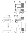
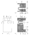
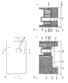
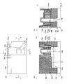
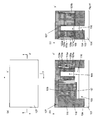
- FIG. 4B is a sectional view taken along line X-X ′ in FIG.
- FIG. 6C is a sectional view taken along line Y-Y ′ in FIG. (A) is a top view which concerns on the manufacturing method of the semiconductor device which concerns on this invention.
- FIG. 4B is a sectional view taken along line X-X ′ in FIG.
- FIG. 6C is a sectional view taken along line Y-Y ′ in FIG. (A) is a top view which concerns on the manufacturing method of the semiconductor device which concerns on this invention.
- FIG. 4B is a sectional view taken along line X-X ′ in FIG. FIG.
- FIG. 6C is a sectional view taken along line Y-Y ′ in FIG. (A) is a top view which concerns on the manufacturing method of the semiconductor device which concerns on this invention.
- FIG. 4B is a sectional view taken along line X-X ′ in FIG.
- FIG. 6C is a sectional view taken along line Y-Y ′ in FIG. (A) is a top view which concerns on the manufacturing method of the semiconductor device which concerns on this invention.
- FIG. 4B is a sectional view taken along line X-X ′ in FIG.
- FIG. 6C is a sectional view taken along line Y-Y ′ in FIG. (A) is a top view which concerns on the manufacturing method of the semiconductor device which concerns on this invention.
- FIG. 4B is a sectional view taken along line X-X ′ in FIG.
- FIG. 6C is a sectional view taken along line Y-Y ′ in FIG. (A) is a top view which concerns on the manufacturing method of the
- FIG. 4B is a sectional view taken along line X-X ′ in FIG.
- FIG. 6C is a sectional view taken along line Y-Y ′ in FIG. (A) is a top view which concerns on the manufacturing method of the semiconductor device which concerns on this invention.
- FIG. 4B is a sectional view taken along line X-X ′ in FIG.
- FIG. 6C is a sectional view taken along line Y-Y ′ in FIG. (A) is a top view which concerns on the manufacturing method of the semiconductor device which concerns on this invention.
- FIG. 4B is a sectional view taken along line X-X ′ in FIG.
- FIG. 6C is a sectional view taken along line Y-Y ′ in FIG.
- FIG. 4B is a sectional view taken along line X-X ′ in FIG.
- FIG. 6C is a sectional view taken along line Y-Y ′ in FIG. (A) is a top view which concerns on the manufacturing method of the semiconductor device which concerns on this invention.
- FIG. 4B is a sectional view taken along line X-X ′ in FIG.
- FIG. 6C is a sectional view taken along line Y-Y ′ in FIG. (A) is a top view which concerns on the manufacturing method of the semiconductor device which concerns on this invention.
- FIG. 4B is a sectional view taken along line X-X ′ in FIG. FIG.
- FIG. 6C is a sectional view taken along line Y-Y ′ in FIG. (A) is a top view which concerns on the manufacturing method of the semiconductor device which concerns on this invention.
- FIG. 4B is a sectional view taken along line X-X ′ in FIG.
- FIG. 6C is a sectional view taken along line Y-Y ′ in FIG.
- the semiconductor substrate is silicon, but other semiconductors may be used as long as they are semiconductors.
- a first resist 102 for forming a fin-like silicon layer is formed on the silicon substrate 101.
- the silicon substrate 101 is etched to form a fin-like silicon layer 103.
- the fin-like silicon layer is formed using a resist as a mask this time, a hard mask such as an oxide film or a nitride film may be used.
- the first resist 102 is removed.
- a first insulating film 104 is deposited around the fin-like silicon layer 103.
- An oxide film formed by high-density plasma or an oxide film formed by low-pressure CVD (Chemical Vapor Deposition) may be used as the first insulating film.
- the first insulating film 104 is etched back to expose the upper portion of the fin-like silicon layer 103.
- the process up to here is the same as the manufacturing method of the fin-like silicon layer of Non-Patent Document 2.
- the first step of forming the fin-like semiconductor layer on the semiconductor substrate and forming the first insulating film around the fin-like semiconductor layer is shown.
- a second insulating film is formed around the fin-like semiconductor layer, a first polysilicon is deposited and planarized on the second insulating film, and a third is formed on the first polysilicon.
- a second resist for forming a gate wiring and a columnar semiconductor layer is formed in a direction perpendicular to the direction of the fin-shaped semiconductor layer, and the third insulating film and the first insulating film are formed. 1 polysilicon, the second insulating film, and the fin-like semiconductor layer are etched, whereby a columnar semiconductor layer, a first dummy gate made of the first polysilicon, and a first insulating film made of the third insulating film.
- the 2nd process of forming a hard mask is shown.
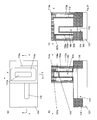
- a second insulating film 105 is formed around the fin-like silicon layer 103.
- the second insulating film 105 is preferably an oxide film.
- a first polysilicon 106 is deposited on the second insulating film 105 and planarized.
- a third insulating film 107 is formed on the first polysilicon 106.
- the third insulating film 107 is preferably a nitride film.
- a second resist 108 for forming a gate wiring and a columnar silicon layer is formed in a direction perpendicular to the direction of the fin-shaped silicon layer 103.
- the third insulating film 107 As shown in FIG. 11, by etching the third insulating film 107, the first polysilicon 106, the second insulating film 105, and the fin-like silicon layer 103, the columnar silicon layer 109 and the first silicon layer 109 are etched.
- a first dummy gate 106a made of one polysilicon and a first hard mask 107a made of a third insulating film are formed.
- the second resist 108 is removed.
- the second insulating film is formed around the fin-like semiconductor layer, the first polysilicon is deposited and planarized on the second insulating film, and the third polysilicon is formed on the first polysilicon.
- a second resist for forming a gate wiring and a columnar semiconductor layer is formed in a direction perpendicular to the direction of the fin-shaped semiconductor layer, and the third insulating film and the first insulating film are formed. 1 polysilicon, the second insulating film, and the fin-like semiconductor layer are etched, whereby a columnar semiconductor layer, a first dummy gate made of the first polysilicon, and a first insulating film made of the third insulating film.
- a second step of forming a hard mask is shown.
- a fourth insulating film is formed around the columnar semiconductor layer and the first dummy gate, and second polysilicon is deposited around the fourth insulating film. Planarizing, etching back, exposing the first hard mask, depositing a sixth insulating film, and etching to form a second hard mask on a sidewall of the first hard mask; A third step of forming a second dummy gate by etching the second polysilicon to remain on the side walls of the first dummy gate and the columnar semiconductor layer is shown.
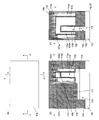
- a fourth insulating film 110 is formed around the columnar silicon layer 109 and the first dummy gate 106a.
- the fourth insulating film 110 is preferably an oxide film.
- a second polysilicon 113 is deposited around the fourth insulating film 110 and planarized.
- the second polysilicon 113 is etched back to expose the first hard mask 107a.
- a sixth insulating film 114 is deposited.
- the sixth insulating film 114 is preferably a nitride film.
- a second hard mask 114a is formed on the sidewall of the first hard mask 107a.
- the second polysilicon 113 is etched to remain on the side walls of the first dummy gate 106a and the columnar semiconductor layer 109, thereby forming a second dummy gate 113a.
- the area of the upper surface of the second dummy gate 113a can be made larger than the area of the lower surface of the second dummy gate 113a by using reverse taper etching.
- the fourth insulating film is formed around the columnar semiconductor layer and the first dummy gate, and the second polysilicon is deposited around the fourth insulating film. Planarizing, etching back, exposing the first hard mask, depositing a sixth insulating film, and etching to form a second hard mask on a sidewall of the first hard mask;
- a third step is shown in which the second dummy gate is formed by etching the second polysilicon so as to remain on the side walls of the first dummy gate and the columnar semiconductor layer.
- a sidewall made of a fifth insulating film is formed around the second dummy gate to form a sidewall made of a fifth insulating film, and the upper part of the fin-like semiconductor layer and the columnar semiconductor are formed.
- a fourth step is shown in which a second diffusion layer is formed below the layer, and a compound of a metal and a semiconductor is formed on the second diffusion layer.
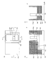
- a fifth insulating film 115 is formed around the second dummy gate 113a.
- the fifth insulating film 115 is preferably a nitride film.
- the fifth insulating film 115 is etched and left in the shape of a sidewall to form a sidewall 115a made of the fifth insulating film.
- impurities are introduced to form a second diffusion layer 116 above the fin-like silicon layer 103 and below the columnar silicon layer 109.
- a second diffusion layer 116 above the fin-like silicon layer 103 and below the columnar silicon layer 109.
- boron In the case of a p-type diffusion layer, it is preferable to introduce boron. Impurity introduction may be performed before the fifth insulating film is formed.
- a metal-semiconductor compound 117 is formed on the second diffusion layer 116.
- the first and second hard masks 107 a and 114 a prevent the formation of a compound of a metal and a semiconductor on the first and second dummy gates 106 a and 113 a, and the fin-like semiconductor layer 103 is formed. Only a compound of a metal and a semiconductor can be formed.
- a sidewall made of a fifth insulating film is formed around the second dummy gate to form a sidewall made of the fifth insulating film, and the upper part of the fin-like semiconductor layer and the columnar semiconductor are formed.
- a fourth step is shown in which a second diffusion layer is formed below the layer, and a metal and semiconductor compound is formed on the second diffusion layer.
- an interlayer insulating film is deposited, the second dummy gate and the upper portion of the first dummy gate are exposed, and the second dummy gate and the first dummy gate are formed.
- 5 shows a fifth step of removing, forming a first gate insulating film around the columnar semiconductor layer and inside the fifth insulating film, depositing a first metal, and forming a gate electrode and a gate wiring. .
- a contact stopper film 118 is deposited, and an interlayer insulating film 119 is deposited.
- the contact stopper film 118 is preferably a nitride film.
- chemical mechanical polishing is performed to expose the upper portions of the second dummy gate 113a and the first dummy gate 106a.
- the second dummy gate 113a and the first dummy gate 106a are removed.
- the second insulating film 105 and the fourth insulating film 110 are removed.
- a first gate insulating film 120 is formed around the columnar silicon layer 109 and inside the fifth insulating film 115a.
- the first metal 121 is deposited.
- the first metal 121 is etched back to expose the upper portion of the columnar silicon layer 109.
- a gate electrode 121 a is formed around the columnar silicon layer 109.
- the gate wiring 121b is formed.
- the gate electrode 121a and the gate wiring 121b are insulated from the columnar silicon layer 109 and the fin-shaped silicon layer 103 by the first gate insulating film 120 formed around and at the bottom of the gate electrode 121a and the gate wiring 121b. be able to.
- a fifth step is shown in which a first gate insulating film is formed around the columnar semiconductor layer and inside the fifth insulating film, a first metal is deposited, and a gate electrode and a gate wiring are formed. It was done.
- a second gate insulating film is deposited around the columnar semiconductor layer, on the gate electrode, and on the gate wiring, and a part of the second gate insulating film on the gate wiring is formed.
- Depositing a second metal performing etch back, removing the second gate insulating film on the columnar semiconductor layer, depositing a third metal, and depositing the third metal and the second metal
- the second metal connects the first contact that surrounds the upper sidewall of the columnar semiconductor layer, the upper portion of the first contact, and the upper portion of the columnar semiconductor layer.
- the exposed first gate insulating film 120 is removed.
- the first gate insulating film 120 becomes the first gate insulating film 120a.
- a second gate insulating film 122 is deposited around the columnar silicon layer 109, on the gate electrode 121a, and on the gate wiring 121b.
- a third resist 123 for removing a part of the second gate insulating film 122 on the gate wiring 121b is formed.
- the second metal 124 is deposited.
- the metal work function of the second metal 124 is preferably between 4.0 eV and 4.2 eV when the transistor is n-type.
- the work function of the second metal 124 is preferably between 5.0 eV and 5.2 eV when the transistor is p-type.
- the second metal 124 is etched back to form contact lines 124a.
- the second gate insulating film 122 on the columnar silicon layer 109 is removed.
- the second gate insulating film 122 becomes the second gate insulating film 122a.
- a fourth resist 125 for forming contact holes is formed.
- the contact hole 126 is formed by etching the interlayer insulating film 119 and the contact stopper film 118.
- the fourth resist 125 is removed.
- a third metal 127 is deposited. Thereby, the third contact 128 is formed.
- the third metal 127 and the contact line 124a are etched to form the second metal on the first contact 124b surrounding the columnar silicon layer 109 and the gate wiring 121b.
- the second contact 124c made of the second metal and the metal wiring 127a, 128b, 128c are formed.
- the upper part of the first contact 124b and the upper part of the columnar silicon layer 109 are connected by a metal wiring 127b.
- a second gate insulating film is deposited around the columnar semiconductor layer, on the gate electrode, and on the gate wiring, and a part of the second gate insulating film on the gate wiring is formed.
- Depositing a second metal performing etch back, removing the second gate insulating film on the columnar semiconductor layer, depositing a third metal, and depositing the third metal and the second metal
- the second metal connects the first contact that surrounds the upper sidewall of the columnar semiconductor layer, the upper portion of the first contact, and the upper portion of the columnar semiconductor layer.
- a method for manufacturing SGT which is a gate last process, was formed by forming a fin-like semiconductor layer, a columnar semiconductor layer, a gate electrode and a gate wiring with two masks.
- FIG. 1 shows the structure of a semiconductor device obtained by the above manufacturing method.
- the semiconductor device of FIG. 1 is formed on the fin-like silicon layer 103, the first insulating film 104 formed around the fin-like silicon layer, and the fin-like silicon layer 103.
- Columnar silicon layer 109, first gate insulating film 120a formed around columnar silicon layer 109, gate electrode 121a made of metal formed around first gate insulating film 120a, Gate wiring 121b made of a metal extending in a direction orthogonal to the fin-like silicon layer 103 connected to the gate electrode 121a, and the first and second gate electrodes 121a and the gate wiring 121b are formed around and at the bottom.
- the first contact 124b, the upper part of the first contact 124b, and the upper part of the columnar silicon layer 109 are connected, and the area of the upper surface of the gate electrode 121a and the gate wiring 121b is It is larger than the area of the lower surface of the gate electrode 121a and the gate wiring 121b.
- the gate electrode 121a and the gate wiring 121b can be insulated from the columnar silicon layer 109 and the fin-shaped silicon layer 103 by the gate insulating film 120a formed around and at the bottom of the gate electrode 121a and the gate wiring 121b. it can.
Landscapes
- Engineering & Computer Science (AREA)
- Power Engineering (AREA)
- Microelectronics & Electronic Packaging (AREA)
- Computer Hardware Design (AREA)
- Condensed Matter Physics & Semiconductors (AREA)
- General Physics & Mathematics (AREA)
- Physics & Mathematics (AREA)
- Ceramic Engineering (AREA)
- Manufacturing & Machinery (AREA)
- Chemical & Material Sciences (AREA)
- Materials Engineering (AREA)
- Crystallography & Structural Chemistry (AREA)
- Nanotechnology (AREA)
- Composite Materials (AREA)
- Insulated Gate Type Field-Effect Transistor (AREA)
- Electrodes Of Semiconductors (AREA)
Abstract
L'invention concerne : un procédé de fabrication de transistor à grille périphérique (SGT), c'est-à-dire un processus de dernière grille, une couche semi-conductrice de type ailette, une couche semi-conductrice columnaire, une électrode de grille et un câblage de grille étant formés à l'aide de deux masques ; une structure SGT obtenue en tant que résultat de la mise en œuvre du procédé de fabrication de SGT. Ce procédé comprend les étapes suivantes : la formation d'un premier film isolant autour d'une couche semi-conductrice de type ailette sur un substrat de semi-conducteur ; la formation d'une première grille fictive formée d'une couche semi-conductrice columnaire et d'un premier polysilicium, et la formation d'un premier masque dur formé d'un troisième film isolant ; la formation d'un second masque dur et d'une seconde grille fictive ; la formation d'une paroi latérale, formée d'un cinquième film isolant, et d'une seconde couche de diffusion ; la formation d'une électrode de grille et d'un câblage de grille ; la formation d'un premier contact ayant un second métal entourant une paroi latérale supérieure de la couche semi-conductrice columnaire, connectant ensemble une partie supérieure du premier contact et une partie supérieure de la couche semi-conductrice columnaire, et la formation d'un deuxième contact formé du second métal formé sur le câblage de grille.
Priority Applications (5)
| Application Number | Priority Date | Filing Date | Title |
|---|---|---|---|
| JP2015520734A JP5822326B1 (ja) | 2014-02-18 | 2014-02-18 | 半導体装置の製造方法、及び、半導体装置 |
| PCT/JP2014/053746 WO2015125205A1 (fr) | 2014-02-18 | 2014-02-18 | Procédé de fabrication de dispositif à semi-conducteurs et dispositif à semi-conducteurs |
| US15/143,732 US9640628B2 (en) | 2014-02-18 | 2016-05-02 | Semiconductor device having fin-shaped semiconductor layer |
| US15/467,627 US9812547B2 (en) | 2014-02-18 | 2017-03-23 | Semiconductor device having fin-shaped semiconductor layer |
| US15/467,676 US9755053B2 (en) | 2014-02-18 | 2017-03-23 | Semiconductor device having fin-shaped semiconductor layer |
Applications Claiming Priority (1)
| Application Number | Priority Date | Filing Date | Title |
|---|---|---|---|
| PCT/JP2014/053746 WO2015125205A1 (fr) | 2014-02-18 | 2014-02-18 | Procédé de fabrication de dispositif à semi-conducteurs et dispositif à semi-conducteurs |
Related Child Applications (1)
| Application Number | Title | Priority Date | Filing Date |
|---|---|---|---|
| US15/143,732 Continuation US9640628B2 (en) | 2014-02-18 | 2016-05-02 | Semiconductor device having fin-shaped semiconductor layer |
Publications (1)
| Publication Number | Publication Date |
|---|---|
| WO2015125205A1 true WO2015125205A1 (fr) | 2015-08-27 |
Family
ID=53877746
Family Applications (1)
| Application Number | Title | Priority Date | Filing Date |
|---|---|---|---|
| PCT/JP2014/053746 WO2015125205A1 (fr) | 2014-02-18 | 2014-02-18 | Procédé de fabrication de dispositif à semi-conducteurs et dispositif à semi-conducteurs |
Country Status (3)
| Country | Link |
|---|---|
| US (3) | US9640628B2 (fr) |
| JP (1) | JP5822326B1 (fr) |
| WO (1) | WO2015125205A1 (fr) |
Families Citing this family (7)
| Publication number | Priority date | Publication date | Assignee | Title |
|---|---|---|---|---|
| JP5779739B1 (ja) * | 2014-02-18 | 2015-09-16 | ユニサンティス エレクトロニクス シンガポール プライベート リミテッドUnisantis Electronics Singapore Pte Ltd. | 半導体装置の製造方法、及び、半導体装置 |
| JP5822326B1 (ja) * | 2014-02-18 | 2015-11-24 | ユニサンティス エレクトロニクス シンガポール プライベート リミテッドUnisantis Electronics Singapore Pte Ltd. | 半導体装置の製造方法、及び、半導体装置 |
| JP5838530B1 (ja) * | 2014-03-05 | 2016-01-06 | ユニサンティス エレクトロニクス シンガポール プライベート リミテッドUnisantis Electronics Singapore Pte Ltd. | 半導体装置の製造方法、及び、半導体装置 |
| WO2015132913A1 (fr) * | 2014-03-05 | 2015-09-11 | ユニサンティス エレクトロニクス シンガポール プライベート リミテッド | Procédé de fabrication de dispositif semi-conducteur et dispositif semi-conducteur |
| US9722048B1 (en) * | 2016-03-28 | 2017-08-01 | International Business Machines Corporation | Vertical transistors with reduced bottom electrode series resistance |
| US20220384446A1 (en) * | 2020-12-25 | 2022-12-01 | Unisantis Electronics Singapore Pte. Ltd. | Method for manufacturing memory device using semiconductor element |
| CN114784006A (zh) * | 2022-04-26 | 2022-07-22 | 长鑫存储技术有限公司 | 半导体结构及其制造方法 |
Citations (4)
| Publication number | Priority date | Publication date | Assignee | Title |
|---|---|---|---|---|
| JP2009070975A (ja) * | 2007-09-12 | 2009-04-02 | Elpida Memory Inc | 半導体装置およびその製造方法 |
| JP2011040682A (ja) * | 2009-08-18 | 2011-02-24 | Unisantis Electronics Japan Ltd | 半導体装置とその製造方法 |
| JP2013239622A (ja) * | 2012-05-16 | 2013-11-28 | Toshiba Corp | 不揮発性半導体記憶装置及びその製造方法 |
| WO2014024266A1 (fr) * | 2012-08-08 | 2014-02-13 | ユニサンティス エレクトロニクス シンガポール プライベート リミテッド | Procédé de fabrication de dispositif semi-conducteur et dispositif semi-conducteur |
Family Cites Families (23)
| Publication number | Priority date | Publication date | Assignee | Title |
|---|---|---|---|---|
| JP2703970B2 (ja) | 1989-01-17 | 1998-01-26 | 株式会社東芝 | Mos型半導体装置 |
| JP3057661B2 (ja) | 1988-09-06 | 2000-07-04 | 株式会社東芝 | 半導体装置 |
| JP2950558B2 (ja) | 1989-11-01 | 1999-09-20 | 株式会社東芝 | 半導体装置 |
| JPH11297984A (ja) | 1998-04-07 | 1999-10-29 | Seiko Epson Corp | Ldd型mosトランジスタの構造および形成方法 |
| US6891234B1 (en) | 2004-01-07 | 2005-05-10 | Acorn Technologies, Inc. | Transistor with workfunction-induced charge layer |
| JP4108537B2 (ja) * | 2003-05-28 | 2008-06-25 | 富士雄 舛岡 | 半導体装置 |
| US8598650B2 (en) * | 2008-01-29 | 2013-12-03 | Unisantis Electronics Singapore Pte Ltd. | Semiconductor device and production method therefor |
| JP4316658B2 (ja) | 2008-01-29 | 2009-08-19 | 日本ユニサンティスエレクトロニクス株式会社 | 半導体装置の製造方法 |
| US8513717B2 (en) * | 2011-01-18 | 2013-08-20 | Unisantis Electronics Singapore Pte. Ltd. | Semiconductor device and method for manufacturing the same |
| US8564034B2 (en) * | 2011-09-08 | 2013-10-22 | Unisantis Electronics Singapore Pte. Ltd. | Solid-state imaging device |
| US8669601B2 (en) * | 2011-09-15 | 2014-03-11 | Unisantis Electronics Singapore Pte. Ltd. | Method for producing semiconductor device and semiconductor device having pillar-shaped semiconductor |
| US8735971B2 (en) * | 2011-12-02 | 2014-05-27 | Unisantis Electronics Singapore Pte. Ltd. | Method for producing semiconductor device and semiconductor device |
| US8772175B2 (en) * | 2011-12-19 | 2014-07-08 | Unisantis Electronics Singapore Pte. Ltd. | Method for manufacturing semiconductor device and semiconductor device |
| KR101849688B1 (ko) * | 2011-12-20 | 2018-04-18 | 인텔 코포레이션 | 반도체 구조물 |
| US8877578B2 (en) * | 2012-05-18 | 2014-11-04 | Unisantis Electronics Singapore Pte. Ltd. | Method for producing semiconductor device and semiconductor device |
| US8697511B2 (en) * | 2012-05-18 | 2014-04-15 | Unisantis Electronics Singapore Pte. Ltd. | Method for producing semiconductor device and semiconductor device |
| US9000513B2 (en) * | 2012-11-12 | 2015-04-07 | Unisantis Electronics Singapore Pte. Ltd. | Method for manufacturing a semiconductor device and semiconductor device with surrounding gate transistor |
| JP5680801B1 (ja) * | 2013-06-10 | 2015-03-04 | ユニサンティス エレクトロニクス シンガポール プライベート リミテッドUnisantis Electronics Singapore Pte Ltd. | 半導体装置の製造方法、及び、半導体装置 |
| WO2014203304A1 (fr) * | 2013-06-17 | 2014-12-24 | ユニサンティス エレクトロニクス シンガポール プライベート リミテッド | Dispositif à semi-conducteurs ainsi que procédé de fabrication de celui-ci |
| WO2015008387A1 (fr) * | 2013-07-19 | 2015-01-22 | ユニサンティス エレクトロニクス シンガポール プライベート リミテッド | Dispositif à semi-conducteurs, et procédé de fabrication de celui-ci |
| JP5759077B1 (ja) * | 2013-08-07 | 2015-08-05 | ユニサンティス エレクトロニクス シンガポール プライベート リミテッドUnisantis Electronics Singapore Pte Ltd. | 半導体装置の製造方法、及び、半導体装置 |
| JP5779739B1 (ja) * | 2014-02-18 | 2015-09-16 | ユニサンティス エレクトロニクス シンガポール プライベート リミテッドUnisantis Electronics Singapore Pte Ltd. | 半導体装置の製造方法、及び、半導体装置 |
| JP5822326B1 (ja) * | 2014-02-18 | 2015-11-24 | ユニサンティス エレクトロニクス シンガポール プライベート リミテッドUnisantis Electronics Singapore Pte Ltd. | 半導体装置の製造方法、及び、半導体装置 |
-
2014
- 2014-02-18 JP JP2015520734A patent/JP5822326B1/ja active Active
- 2014-02-18 WO PCT/JP2014/053746 patent/WO2015125205A1/fr active Application Filing
-
2016
- 2016-05-02 US US15/143,732 patent/US9640628B2/en active Active
-
2017
- 2017-03-23 US US15/467,627 patent/US9812547B2/en active Active
- 2017-03-23 US US15/467,676 patent/US9755053B2/en active Active
Patent Citations (4)
| Publication number | Priority date | Publication date | Assignee | Title |
|---|---|---|---|---|
| JP2009070975A (ja) * | 2007-09-12 | 2009-04-02 | Elpida Memory Inc | 半導体装置およびその製造方法 |
| JP2011040682A (ja) * | 2009-08-18 | 2011-02-24 | Unisantis Electronics Japan Ltd | 半導体装置とその製造方法 |
| JP2013239622A (ja) * | 2012-05-16 | 2013-11-28 | Toshiba Corp | 不揮発性半導体記憶装置及びその製造方法 |
| WO2014024266A1 (fr) * | 2012-08-08 | 2014-02-13 | ユニサンティス エレクトロニクス シンガポール プライベート リミテッド | Procédé de fabrication de dispositif semi-conducteur et dispositif semi-conducteur |
Also Published As
| Publication number | Publication date |
|---|---|
| US20170194460A1 (en) | 2017-07-06 |
| US9812547B2 (en) | 2017-11-07 |
| US20170194453A1 (en) | 2017-07-06 |
| US9755053B2 (en) | 2017-09-05 |
| US9640628B2 (en) | 2017-05-02 |
| US20160247892A1 (en) | 2016-08-25 |
| JPWO2015125205A1 (ja) | 2017-03-30 |
| JP5822326B1 (ja) | 2015-11-24 |
Similar Documents
| Publication | Publication Date | Title |
|---|---|---|
| JP5822326B1 (ja) | 半導体装置の製造方法、及び、半導体装置 | |
| JP5731073B1 (ja) | 半導体装置の製造方法、及び、半導体装置 | |
| JP5759077B1 (ja) | 半導体装置の製造方法、及び、半導体装置 | |
| JP5779739B1 (ja) | 半導体装置の製造方法、及び、半導体装置 | |
| JP5775650B1 (ja) | 半導体装置の製造方法、及び、半導体装置 | |
| JP5838529B1 (ja) | 半導体装置の製造方法、及び、半導体装置 | |
| JP5838530B1 (ja) | 半導体装置の製造方法、及び、半導体装置 | |
| JP5902868B1 (ja) | 半導体装置の製造方法、及び、半導体装置 | |
| JP5680801B1 (ja) | 半導体装置の製造方法、及び、半導体装置 | |
| JP5740535B1 (ja) | 半導体装置の製造方法、及び、半導体装置 | |
| JP6033938B2 (ja) | 半導体装置の製造方法、及び、半導体装置 | |
| JP6154051B2 (ja) | 半導体装置の製造方法、及び、半導体装置 | |
| JP5989197B2 (ja) | 半導体装置の製造方法、及び、半導体装置 | |
| JP6329299B2 (ja) | 半導体装置の製造方法、及び、半導体装置 | |
| JP5977865B2 (ja) | 半導体装置の製造方法、及び、半導体装置 | |
| JP6080989B2 (ja) | 半導体装置の製造方法、及び、半導体装置 | |
| JP5869166B2 (ja) | 半導体装置の製造方法、及び、半導体装置 | |
| JP6285393B2 (ja) | 半導体装置の製造方法、及び、半導体装置 | |
| JP5861197B2 (ja) | 半導体装置の製造方法、及び、半導体装置 | |
| JP2016105500A (ja) | 半導体装置の製造方法、及び、半導体装置 | |
| JP2016086194A (ja) | 半導体装置の製造方法、及び、半導体装置 | |
| JP2015159320A (ja) | 半導体装置の製造方法、及び、半導体装置 | |
| JP2015065456A (ja) | 半導体装置の製造方法、及び、半導体装置 |
Legal Events
| Date | Code | Title | Description |
|---|---|---|---|
| ENP | Entry into the national phase |
Ref document number: 2015520734 Country of ref document: JP Kind code of ref document: A |
|
| 121 | Ep: the epo has been informed by wipo that ep was designated in this application |
Ref document number: 14883317 Country of ref document: EP Kind code of ref document: A1 |
|
| NENP | Non-entry into the national phase |
Ref country code: DE |
|
| 122 | Ep: pct application non-entry in european phase |
Ref document number: 14883317 Country of ref document: EP Kind code of ref document: A1 |