WO2015111242A1 - 放熱部品、放熱部品の製造方法、電子装置、電子装置の製造方法、一体型モジュール、情報処理システム - Google Patents
放熱部品、放熱部品の製造方法、電子装置、電子装置の製造方法、一体型モジュール、情報処理システム Download PDFInfo
- Publication number
- WO2015111242A1 WO2015111242A1 PCT/JP2014/068227 JP2014068227W WO2015111242A1 WO 2015111242 A1 WO2015111242 A1 WO 2015111242A1 JP 2014068227 W JP2014068227 W JP 2014068227W WO 2015111242 A1 WO2015111242 A1 WO 2015111242A1
- Authority
- WO
- WIPO (PCT)
- Prior art keywords
- fin
- main body
- mold
- heat dissipation
- heat
- Prior art date
Links
Images


Classifications
-
- H—ELECTRICITY
- H01—ELECTRIC ELEMENTS
- H01L—SEMICONDUCTOR DEVICES NOT COVERED BY CLASS H10
- H01L23/00—Details of semiconductor or other solid state devices
- H01L23/34—Arrangements for cooling, heating, ventilating or temperature compensation ; Temperature sensing arrangements
- H01L23/36—Selection of materials, or shaping, to facilitate cooling or heating, e.g. heatsinks
-
- H—ELECTRICITY
- H05—ELECTRIC TECHNIQUES NOT OTHERWISE PROVIDED FOR
- H05K—PRINTED CIRCUITS; CASINGS OR CONSTRUCTIONAL DETAILS OF ELECTRIC APPARATUS; MANUFACTURE OF ASSEMBLAGES OF ELECTRICAL COMPONENTS
- H05K7/00—Constructional details common to different types of electric apparatus
- H05K7/20—Modifications to facilitate cooling, ventilating, or heating
- H05K7/2039—Modifications to facilitate cooling, ventilating, or heating characterised by the heat transfer by conduction from the heat generating element to a dissipating body
- H05K7/20436—Inner thermal coupling elements in heat dissipating housings, e.g. protrusions or depressions integrally formed in the housing
-
- G—PHYSICS
- G08—SIGNALLING
- G08G—TRAFFIC CONTROL SYSTEMS
- G08G1/00—Traffic control systems for road vehicles
- G08G1/01—Detecting movement of traffic to be counted or controlled
- G08G1/042—Detecting movement of traffic to be counted or controlled using inductive or magnetic detectors
-
- H—ELECTRICITY
- H01—ELECTRIC ELEMENTS
- H01L—SEMICONDUCTOR DEVICES NOT COVERED BY CLASS H10
- H01L21/00—Processes or apparatus adapted for the manufacture or treatment of semiconductor or solid state devices or of parts thereof
- H01L21/02—Manufacture or treatment of semiconductor devices or of parts thereof
- H01L21/04—Manufacture or treatment of semiconductor devices or of parts thereof the devices having at least one potential-jump barrier or surface barrier, e.g. PN junction, depletion layer or carrier concentration layer
- H01L21/48—Manufacture or treatment of parts, e.g. containers, prior to assembly of the devices, using processes not provided for in a single one of the subgroups H01L21/06 - H01L21/326
- H01L21/4814—Conductive parts
- H01L21/4871—Bases, plates or heatsinks
- H01L21/4878—Mechanical treatment, e.g. deforming
-
- H—ELECTRICITY
- H01—ELECTRIC ELEMENTS
- H01L—SEMICONDUCTOR DEVICES NOT COVERED BY CLASS H10
- H01L21/00—Processes or apparatus adapted for the manufacture or treatment of semiconductor or solid state devices or of parts thereof
- H01L21/02—Manufacture or treatment of semiconductor devices or of parts thereof
- H01L21/04—Manufacture or treatment of semiconductor devices or of parts thereof the devices having at least one potential-jump barrier or surface barrier, e.g. PN junction, depletion layer or carrier concentration layer
- H01L21/48—Manufacture or treatment of parts, e.g. containers, prior to assembly of the devices, using processes not provided for in a single one of the subgroups H01L21/06 - H01L21/326
- H01L21/4814—Conductive parts
- H01L21/4871—Bases, plates or heatsinks
- H01L21/4882—Assembly of heatsink parts
-
- H—ELECTRICITY
- H01—ELECTRIC ELEMENTS
- H01L—SEMICONDUCTOR DEVICES NOT COVERED BY CLASS H10
- H01L21/00—Processes or apparatus adapted for the manufacture or treatment of semiconductor or solid state devices or of parts thereof
- H01L21/02—Manufacture or treatment of semiconductor devices or of parts thereof
- H01L21/04—Manufacture or treatment of semiconductor devices or of parts thereof the devices having at least one potential-jump barrier or surface barrier, e.g. PN junction, depletion layer or carrier concentration layer
- H01L21/50—Assembly of semiconductor devices using processes or apparatus not provided for in a single one of the subgroups H01L21/06 - H01L21/326, e.g. sealing of a cap to a base of a container
- H01L21/56—Encapsulations, e.g. encapsulation layers, coatings
- H01L21/565—Moulds
-
- H—ELECTRICITY
- H01—ELECTRIC ELEMENTS
- H01L—SEMICONDUCTOR DEVICES NOT COVERED BY CLASS H10
- H01L23/00—Details of semiconductor or other solid state devices
- H01L23/28—Encapsulations, e.g. encapsulating layers, coatings, e.g. for protection
- H01L23/31—Encapsulations, e.g. encapsulating layers, coatings, e.g. for protection characterised by the arrangement or shape
- H01L23/3107—Encapsulations, e.g. encapsulating layers, coatings, e.g. for protection characterised by the arrangement or shape the device being completely enclosed
- H01L23/3121—Encapsulations, e.g. encapsulating layers, coatings, e.g. for protection characterised by the arrangement or shape the device being completely enclosed a substrate forming part of the encapsulation
-
- H—ELECTRICITY
- H01—ELECTRIC ELEMENTS
- H01L—SEMICONDUCTOR DEVICES NOT COVERED BY CLASS H10
- H01L23/00—Details of semiconductor or other solid state devices
- H01L23/34—Arrangements for cooling, heating, ventilating or temperature compensation ; Temperature sensing arrangements
- H01L23/36—Selection of materials, or shaping, to facilitate cooling or heating, e.g. heatsinks
- H01L23/367—Cooling facilitated by shape of device
- H01L23/3675—Cooling facilitated by shape of device characterised by the shape of the housing
-
- H—ELECTRICITY
- H01—ELECTRIC ELEMENTS
- H01L—SEMICONDUCTOR DEVICES NOT COVERED BY CLASS H10
- H01L23/00—Details of semiconductor or other solid state devices
- H01L23/34—Arrangements for cooling, heating, ventilating or temperature compensation ; Temperature sensing arrangements
- H01L23/36—Selection of materials, or shaping, to facilitate cooling or heating, e.g. heatsinks
- H01L23/373—Cooling facilitated by selection of materials for the device or materials for thermal expansion adaptation, e.g. carbon
-
- H—ELECTRICITY
- H01—ELECTRIC ELEMENTS
- H01L—SEMICONDUCTOR DEVICES NOT COVERED BY CLASS H10
- H01L23/00—Details of semiconductor or other solid state devices
- H01L23/34—Arrangements for cooling, heating, ventilating or temperature compensation ; Temperature sensing arrangements
- H01L23/42—Fillings or auxiliary members in containers or encapsulations selected or arranged to facilitate heating or cooling
- H01L23/433—Auxiliary members in containers characterised by their shape, e.g. pistons
- H01L23/4334—Auxiliary members in encapsulations
-
- H—ELECTRICITY
- H01—ELECTRIC ELEMENTS
- H01L—SEMICONDUCTOR DEVICES NOT COVERED BY CLASS H10
- H01L24/00—Arrangements for connecting or disconnecting semiconductor or solid-state bodies; Methods or apparatus related thereto
- H01L24/01—Means for bonding being attached to, or being formed on, the surface to be connected, e.g. chip-to-package, die-attach, "first-level" interconnects; Manufacturing methods related thereto
- H01L24/42—Wire connectors; Manufacturing methods related thereto
- H01L24/47—Structure, shape, material or disposition of the wire connectors after the connecting process
- H01L24/48—Structure, shape, material or disposition of the wire connectors after the connecting process of an individual wire connector
-
- H—ELECTRICITY
- H10—SEMICONDUCTOR DEVICES; ELECTRIC SOLID-STATE DEVICES NOT OTHERWISE PROVIDED FOR
- H10N—ELECTRIC SOLID-STATE DEVICES NOT OTHERWISE PROVIDED FOR
- H10N10/00—Thermoelectric devices comprising a junction of dissimilar materials, i.e. devices exhibiting Seebeck or Peltier effects
- H10N10/10—Thermoelectric devices comprising a junction of dissimilar materials, i.e. devices exhibiting Seebeck or Peltier effects operating with only the Peltier or Seebeck effects
- H10N10/13—Thermoelectric devices comprising a junction of dissimilar materials, i.e. devices exhibiting Seebeck or Peltier effects operating with only the Peltier or Seebeck effects characterised by the heat-exchanging means at the junction
-
- H—ELECTRICITY
- H10—SEMICONDUCTOR DEVICES; ELECTRIC SOLID-STATE DEVICES NOT OTHERWISE PROVIDED FOR
- H10N—ELECTRIC SOLID-STATE DEVICES NOT OTHERWISE PROVIDED FOR
- H10N10/00—Thermoelectric devices comprising a junction of dissimilar materials, i.e. devices exhibiting Seebeck or Peltier effects
- H10N10/10—Thermoelectric devices comprising a junction of dissimilar materials, i.e. devices exhibiting Seebeck or Peltier effects operating with only the Peltier or Seebeck effects
- H10N10/17—Thermoelectric devices comprising a junction of dissimilar materials, i.e. devices exhibiting Seebeck or Peltier effects operating with only the Peltier or Seebeck effects characterised by the structure or configuration of the cell or thermocouple forming the device
-
- H—ELECTRICITY
- H10—SEMICONDUCTOR DEVICES; ELECTRIC SOLID-STATE DEVICES NOT OTHERWISE PROVIDED FOR
- H10N—ELECTRIC SOLID-STATE DEVICES NOT OTHERWISE PROVIDED FOR
- H10N10/00—Thermoelectric devices comprising a junction of dissimilar materials, i.e. devices exhibiting Seebeck or Peltier effects
- H10N10/80—Constructional details
-
- H—ELECTRICITY
- H10—SEMICONDUCTOR DEVICES; ELECTRIC SOLID-STATE DEVICES NOT OTHERWISE PROVIDED FOR
- H10N—ELECTRIC SOLID-STATE DEVICES NOT OTHERWISE PROVIDED FOR
- H10N19/00—Integrated devices, or assemblies of multiple devices, comprising at least one thermoelectric or thermomagnetic element covered by groups H10N10/00 - H10N15/00
-
- H—ELECTRICITY
- H01—ELECTRIC ELEMENTS
- H01L—SEMICONDUCTOR DEVICES NOT COVERED BY CLASS H10
- H01L2224/00—Indexing scheme for arrangements for connecting or disconnecting semiconductor or solid-state bodies and methods related thereto as covered by H01L24/00
- H01L2224/01—Means for bonding being attached to, or being formed on, the surface to be connected, e.g. chip-to-package, die-attach, "first-level" interconnects; Manufacturing methods related thereto
- H01L2224/42—Wire connectors; Manufacturing methods related thereto
- H01L2224/47—Structure, shape, material or disposition of the wire connectors after the connecting process
- H01L2224/48—Structure, shape, material or disposition of the wire connectors after the connecting process of an individual wire connector
- H01L2224/4805—Shape
- H01L2224/4809—Loop shape
- H01L2224/48091—Arched
-
- H—ELECTRICITY
- H01—ELECTRIC ELEMENTS
- H01L—SEMICONDUCTOR DEVICES NOT COVERED BY CLASS H10
- H01L2224/00—Indexing scheme for arrangements for connecting or disconnecting semiconductor or solid-state bodies and methods related thereto as covered by H01L24/00
- H01L2224/01—Means for bonding being attached to, or being formed on, the surface to be connected, e.g. chip-to-package, die-attach, "first-level" interconnects; Manufacturing methods related thereto
- H01L2224/42—Wire connectors; Manufacturing methods related thereto
- H01L2224/47—Structure, shape, material or disposition of the wire connectors after the connecting process
- H01L2224/48—Structure, shape, material or disposition of the wire connectors after the connecting process of an individual wire connector
- H01L2224/481—Disposition
- H01L2224/48105—Connecting bonding areas at different heights
- H01L2224/48106—Connecting bonding areas at different heights the connector being orthogonal to a side surface of the semiconductor or solid-state body, e.g. parallel layout
-
- H—ELECTRICITY
- H01—ELECTRIC ELEMENTS
- H01L—SEMICONDUCTOR DEVICES NOT COVERED BY CLASS H10
- H01L2224/00—Indexing scheme for arrangements for connecting or disconnecting semiconductor or solid-state bodies and methods related thereto as covered by H01L24/00
- H01L2224/01—Means for bonding being attached to, or being formed on, the surface to be connected, e.g. chip-to-package, die-attach, "first-level" interconnects; Manufacturing methods related thereto
- H01L2224/42—Wire connectors; Manufacturing methods related thereto
- H01L2224/47—Structure, shape, material or disposition of the wire connectors after the connecting process
- H01L2224/48—Structure, shape, material or disposition of the wire connectors after the connecting process of an individual wire connector
- H01L2224/481—Disposition
- H01L2224/48151—Connecting between a semiconductor or solid-state body and an item not being a semiconductor or solid-state body, e.g. chip-to-substrate, chip-to-passive
- H01L2224/48221—Connecting between a semiconductor or solid-state body and an item not being a semiconductor or solid-state body, e.g. chip-to-substrate, chip-to-passive the body and the item being stacked
- H01L2224/48225—Connecting between a semiconductor or solid-state body and an item not being a semiconductor or solid-state body, e.g. chip-to-substrate, chip-to-passive the body and the item being stacked the item being non-metallic, e.g. insulating substrate with or without metallisation
- H01L2224/48227—Connecting between a semiconductor or solid-state body and an item not being a semiconductor or solid-state body, e.g. chip-to-substrate, chip-to-passive the body and the item being stacked the item being non-metallic, e.g. insulating substrate with or without metallisation connecting the wire to a bond pad of the item
-
- H—ELECTRICITY
- H01—ELECTRIC ELEMENTS
- H01L—SEMICONDUCTOR DEVICES NOT COVERED BY CLASS H10
- H01L2224/00—Indexing scheme for arrangements for connecting or disconnecting semiconductor or solid-state bodies and methods related thereto as covered by H01L24/00
- H01L2224/01—Means for bonding being attached to, or being formed on, the surface to be connected, e.g. chip-to-package, die-attach, "first-level" interconnects; Manufacturing methods related thereto
- H01L2224/42—Wire connectors; Manufacturing methods related thereto
- H01L2224/47—Structure, shape, material or disposition of the wire connectors after the connecting process
- H01L2224/48—Structure, shape, material or disposition of the wire connectors after the connecting process of an individual wire connector
- H01L2224/484—Connecting portions
- H01L2224/4847—Connecting portions the connecting portion on the bonding area of the semiconductor or solid-state body being a wedge bond
- H01L2224/48472—Connecting portions the connecting portion on the bonding area of the semiconductor or solid-state body being a wedge bond the other connecting portion not on the bonding area also being a wedge bond, i.e. wedge-to-wedge
-
- H—ELECTRICITY
- H01—ELECTRIC ELEMENTS
- H01L—SEMICONDUCTOR DEVICES NOT COVERED BY CLASS H10
- H01L2224/00—Indexing scheme for arrangements for connecting or disconnecting semiconductor or solid-state bodies and methods related thereto as covered by H01L24/00
- H01L2224/73—Means for bonding being of different types provided for in two or more of groups H01L2224/10, H01L2224/18, H01L2224/26, H01L2224/34, H01L2224/42, H01L2224/50, H01L2224/63, H01L2224/71
- H01L2224/732—Location after the connecting process
- H01L2224/73201—Location after the connecting process on the same surface
- H01L2224/73215—Layer and wire connectors
-
- H—ELECTRICITY
- H01—ELECTRIC ELEMENTS
- H01L—SEMICONDUCTOR DEVICES NOT COVERED BY CLASS H10
- H01L2924/00—Indexing scheme for arrangements or methods for connecting or disconnecting semiconductor or solid-state bodies as covered by H01L24/00
- H01L2924/0001—Technical content checked by a classifier
- H01L2924/00014—Technical content checked by a classifier the subject-matter covered by the group, the symbol of which is combined with the symbol of this group, being disclosed without further technical details
-
- H—ELECTRICITY
- H01—ELECTRIC ELEMENTS
- H01L—SEMICONDUCTOR DEVICES NOT COVERED BY CLASS H10
- H01L2924/00—Indexing scheme for arrangements or methods for connecting or disconnecting semiconductor or solid-state bodies as covered by H01L24/00
- H01L2924/15—Details of package parts other than the semiconductor or other solid state devices to be connected
- H01L2924/181—Encapsulation
- H01L2924/1815—Shape
Definitions
- the technology disclosed in the present application relates to a heat dissipation component, a method for manufacturing a heat dissipation component, an electronic device, a method for manufacturing an electronic device, an integrated module, and an information processing system.
- a heat dissipation component that is thermally connected to the electronic component and radiates heat may be used.
- an electronic device provided with a heat dissipation component as described above can suppress a decrease in the heat dissipation performance of the heat dissipation component.
- the technology disclosed in the present application is, as one aspect, aimed at suppressing a decrease in heat dissipation performance of a heat dissipation component.
- a heat dissipating component including a main body, a heat dissipating material, and a covering.
- the main body is formed of a first material
- the heat dissipation sheet is formed of a second material having a higher thermal conductivity than the first material.
- the heat dissipation sheet is provided in the main body, and includes a fin, another fin thermally connected at positions different from the fin and the top, and a connected portion that thermally connects the fin and the electronic component.
- the covering portion is formed of the first material and covers at least a part of the bottom portion of the groove between the fin and the other fin.
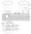
- FIG. 1 is a perspective view of an electronic device according to a first embodiment. It is front sectional drawing of the electronic device which concerns on 1st embodiment. It is a figure explaining the manufacturing method of the electronic device concerning a first embodiment. It is a figure explaining the manufacturing method of the electronic device concerning a first embodiment. It is a figure explaining the manufacturing method of the electronic device concerning a first embodiment. It is a partial expansion perspective view of a heat dissipation sheet concerning a first embodiment. It is a figure explaining the manufacturing method of the electronic device concerning a first embodiment. It is a figure explaining the manufacturing method of the electronic device concerning a first embodiment. It is a figure explaining the manufacturing method of the electronic device concerning a first embodiment. It is a figure showing an information processing system concerning a first embodiment.
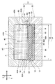
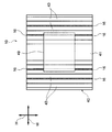
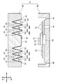
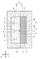
- the electronic device 10 includes a main body 12, a substrate 30, and a heat dissipation sheet 40.
- Arrows W, L, and H shown in the drawings indicate the width direction, the length direction, and the height direction of the electronic device 10, respectively.
- the width direction, the length direction, and the height direction of the electronic device 10 are referred to as a width W direction, a length L direction, and a height H direction.
- the main body 12 has a flat rectangular parallelepiped base 13 and a plurality of convex portions 14 projecting upward from the base 13 in the height H direction.
- the main body 12 is formed by molding as will be described later, and is formed of a resin (eg, polyamide resin) that is an example of the “first material”.
- the substrate 30 is formed in a flat plate shape, and is arranged with the height H direction as the thickness direction.
- Mounted components including a thermoelectric element 31 that is an example of an “electronic component” and a communication component 32 that is an example of a “communication unit” are mounted on the substrate 30.
- the mounting components of the substrate 30 including the thermoelectric element 31 and the communication component 32 are connected by a circuit pattern formed on the substrate 30. As shown in FIG. 2, the mounting components such as the thermoelectric element 31 and the communication component 32 and the substrate 30 are sealed by the base portion 13 of the main body portion 12 made of resin.
- thermoelectric element 31 The heat radiating surface of the thermoelectric element 31 is thermally connected to a connected portion 41 of a heat radiating sheet 40 described later via a connecting member 33 and a heat spreader 34.
- a heat transfer member 35 is disposed on the heat absorption surface side of the thermoelectric element 31.
- the heat transfer member 35 is thermally connected to the heat absorption surface of the thermoelectric element 31.
- a portion 35 ⁇ / b> A opposite to the thermoelectric element 31 in the heat transfer member 35 protrudes from the bottom surface of the main body 12 and is exposed to the outside.
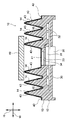
- the heat dissipation sheet 40 is formed of a second material having a higher thermal conductivity than the first material forming the main body 12.
- the material forming the heat dissipation sheet 40 is graphite (carbon).
- the heat dissipation sheet 40 is provided on the upper side in the height H direction of the main body 12 and covers the main body 12 from the upper side in the height H direction.
- a connected portion 41 that is thermally connected to the thermoelectric element 31 is formed at the center in the width W direction of the heat radiating sheet 40. Edges are provided at both ends of the heat radiating sheet 40 in the width W direction. 42 is formed. The connected portion 41 and the edge portion 42 are formed with the height H direction as the thickness direction. The positions (heights) of the connected portion 41 and the edge portion 42 in the height H direction are aligned as an example.
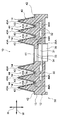
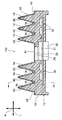
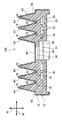
- a plurality of fins 43 are bent and formed on both sides of the connected portion 41 in the heat dissipation sheet 40.
- the plurality of fins 43 are formed with the height H direction as the height direction.
- the fin 43 has a pointed shape (an isosceles triangular cross section) whose width becomes narrower toward the top 43A. As an example, the plurality of fins 43 are aligned at the same height.
- the plurality of fins 43 formed on one side and the other side in the width W direction of the heat dissipation sheet 40 are arranged in the width W direction, and each fin 43 has a length L direction. It extends as the longitudinal direction.
- the length L direction which is the direction in which the fins 43 extend, is an example of a “direction intersecting the direction in which a plurality of fins are arranged”.
- One fin 43 and the other fin 43 are connected by a bottom 44 ⁇ / b> A as an example of being thermally connected at positions different from the top.
- the heat dissipating sheet 40 having the plurality of fins 43, the connected portions 41, and the edge portions 42 is formed by, for example, pressing.
- the inside of the fin 43 is filled with a resin that forms the convex portion 14, and the fin 43 is supported by the convex portion 14 from the inside of the fin 43.
- the electronic device 10 further includes a covering portion 16.
- the covering portion 16 is made of the same material as that of the main body portion 12 and covers the entire bottom portion 44 ⁇ / b> A of the groove 44 formed between the plurality of fins 43.
- a connecting portion 19 is formed between the main body portion 12 and the covering portion 16 during molding, and the main body portion 12 and the covering portion 16 are integrated with each other via the connecting portion 19. It is formed.
- the connection portion 19 (see FIG. 8) is not shown for easy understanding of the internal structure of the electronic device 10.
- the main body 12 and the cover 16 are resin, and are integrated with the heat dissipation sheet 40 by molding.
- the covering portion 16 is formed in a long thin plate shape, and is provided on the bottom portion 44 ⁇ / b> A side in the groove 44. By forming the covering portion 16 to be thin, a portion of the side surface portion 43B of the fin 43 closer to the top portion 43A of the fin 43 than the covering portion 16 is exposed to the outside.
- the remaining structure excluding the thermoelectric element 31, the connection member 33, the heat spreader 34, the heat transfer member 35, and the substrate 30 from the electronic device 10 forms the heat dissipation component 50.
- the heat radiating component 50 includes the main body portion 12, the heat radiating sheet 40, and the plurality of covering portions 16.
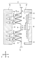
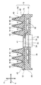
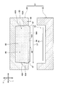
- the mold 51 includes a first mold 52 and a second mold 62.
- the first mold 52 is a fixed mold
- the second mold 62 is a movable mold.
- the first mold 52 is formed with a first cavity 53 that is recessed downward in the height H direction.
- the first cavity 53 has a depth corresponding to the height of the base portion 13 (see FIG. 1).
- the first cavity 53 accommodates the substrate 30 on which the thermoelectric element 31, the communication component 32, the connection member 33, the heat spreader 34, the heat transfer member 35, and the like are mounted.
- the first mold 52 is formed with an injection port 54 for injecting resin into the mold 51 and an exhaust port 55 for venting the air in the mold 51.
- the inlet 54 opens toward the inside of a plurality of second cavities 63 formed in a second mold 62 described later.
- the second mold 62 is formed with a plurality of second cavities 63 arranged in the width W direction and recessed upward in the height H direction.
- Each of the second cavities 63 is formed according to the outer shape and size of the plurality of fins 43 formed on the heat dissipation sheet 40, and has an inverted V-shaped cross section.
- the heat radiation sheet 40 is attached to the second mold 62, and the plurality of fins 43 are accommodated in the plurality of second cavities 63. Pointed portions between the plurality of second cavities 63 are formed as protrusions 64 protruding toward the first mold 52, and are inserted into the grooves 44 between the plurality of fins 43.
- the facing surfaces 65 and 66 facing the connected portion 41 and the edge portion 42 are, for example, aligned at the same height.
- the facing surfaces 65 and 66 abut against the connected portion 41 and the edge portion 42, respectively.
- the bottom 44 ⁇ / b> A of the groove 44 formed in the heat dissipation sheet 40 is positioned lower than the connected portion 41 and the edge portion 42 in the depth direction (height H direction) of the groove 44, and is inserted into the groove 44.
- a gap 68 is formed between the tip 64A and the bottom 44A of the protrusion 64.
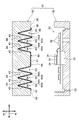
- the end 40 ⁇ / b> A in the length L direction of the heat radiation sheet 40 is linear along the height H direction.
- the side surface 63A in the length L direction of the second cavity 63 is inclined with respect to the height H direction so as to go to the end side in the length L direction as it goes downward in the height H direction. That is, as shown in FIG. 6, the side surface 63A in the length L direction of the second cavity 63 has an inclination angle ⁇ with respect to the height H direction.
- the inclination angle ⁇ (taper) of the second cavity 63 is provided to facilitate removal of the molded product from the second cavity 63.
- the side surface 63A of the second cavity 63 is inclined, so that the length L2 of the heat dissipation sheet 40 in the longitudinal direction is the first cavity 53 and the second cavity 53 for forming the main body 12 as shown in FIG.
- the cavity 63 is shorter than the length L1 in the length L direction.
- the length L1 of the second cavity 63 in the length L direction corresponds to the opening width of the second cavity 63 on the first mold 52 side and the opening width of the first cavity 53 on the second mold 62 side. .
- the electronic device 10 is manufactured in the following manner.
- the substrate 30 on which the thermoelectric element 31, the communication component 32, the connection member 33, the heat spreader 34, the heat transfer member 35 and the like are mounted is a first cavity 53 in the first mold 52. Is housed in. Further, the heat dissipation sheet 40 formed by bending a plurality of fins 43 in advance by press working is accommodated in the second cavity 63 in the second mold 62.
- the heat dissipation sheet 40 is formed in advance so that the length L2 in the length L direction is shorter than the length L1 in the length L direction of the first cavity 53 and the second cavity 63.
- the bottom 44 ⁇ / b> A is located at a lower position in the depth direction (height H direction) of the groove 44 than the tip 64 ⁇ / b> A of the protrusion 64 of the second mold 62 inserted into the groove 44.
- a gap 68 is formed between the tip 64A and the bottom 44A of the projection 64.
- the state in which the first mold 52 and the second mold 62 are combined and fixed in this manner is an example of a “set state”.
- a resin that is an example of the “first material” is injected into the mold 51 from the injection port 54 toward the inside of the fin 43 in a molten state.
- the resin injected into the mold 51 flows from the inside of the fin 43 toward the top portion 43 ⁇ / b> A of the fin 43 and is filled inside the fin 43.
- the fin 43 swells and is in close contact with the inner surface of the second cavity 63.
- through holes through which the resin passes may be formed in the substrate 30 so that the resin injected into the mold 51 can easily flow into the fins 43.
- the resin that has reached the top 43 ⁇ / b> A of the fin 43 rebounds at the top 43 ⁇ / b> A and flows to both ends of the fin 43 in the length L direction.
- the resin that has flowed to the ends on both sides in the length direction of the fin 43 flows out of the fins 43 from the openings on both sides in the length L direction inside the fin 43.
- the resin flowing out of the fins 43 has a gap 69 between the end portion 40A in the length L direction of the heat radiation sheet 40 and the side surface 63A of the second cavity 63, as indicated by an arrow B in FIG.
- the gap 68 between the tip portion 64A and the bottom portion 44A of the protrusion 64 is filled.
- the gap 68 is appropriately dimensioned according to the material and temperature of the molten resin.
- the mold 51 is cooled.
- the mold 51 may be naturally cooled, or may be forcibly cooled by circulating cooling water supplied from the outside through a water cooling pipe provided in the mold 51.
- the base portion 13, the plurality of convex portions 14, and the plurality of covering portions 16 are formed as shown in FIG. It is formed. That is, the base 13 for sealing the thermoelectric element 31 and the substrate 30 is formed by the resin filled in the first cavity 53 of the first mold 52, and the fin 43 is formed by the resin filled inside the fin 43. The convex part 14 to support is formed. Further, the covering portion 16 that covers the entire bottom portion 44A is formed by the resin filled in the gap 68 between the tip end portion 64A and the bottom portion 44A of the protrusion 64 of the second mold 62.
- the gap 69 between the end portion 40A in the length L direction of the heat dissipation sheet 40 and the side surface 63A of the second cavity 63 is filled.
- the connecting portion 19 is formed by the resin thus formed.
- the main body portion 12 and the covering portion 16 are integrally formed via the connecting portion 19.
- the connecting portion 19 covers the heat dissipation sheet 40 from both sides in the length L direction and extends from the main body portion 12 to the top portion 43 ⁇ / b> A of the fin 43.
- the main body 12 and the cover 16 are integrated with the heat dissipation sheet 40 by the above molding.
- the length of the main body 12 in the length L direction is the same as the length L1 of the first cavity 53 and the second cavity 63 in the length L direction.
- the length L1 in the length L direction of the main body 12 is longer than the length L2 in the length L direction of the heat dissipation sheet 40 because the connecting portion 19 is formed in the main body 12.
- the electronic device 10 manufactured as described above is taken out from the mold 51.
- the electronic device 10 includes a main body portion 12 formed of resin by molding and a sheet provided on the main body portion 12. And a heat-dissipating sheet 40 in a single body.
- this electronic device 10 it is not the main body portion 12 formed of a resin having low thermal conductivity but the heat radiating sheet 40 provided in the main body portion 12 that is responsible for heat dissipation. Since this heat radiating sheet 40 has a sheet shape, it is required to be continuous in order to ensure heat radiating properties.
- the bottom portion 44A of the groove 44 is covered with the covering portion 16. Accordingly, even when the foreign matter accumulated in the groove 44 is removed using a cleaning tool such as a brush, the contact between the cleaning tool and the bottom portion 44A is prevented, so that the surface of the bottom portion 44A can be prevented from being damaged. Thereby, even if the heat radiating sheet 40 is formed of, for example, a soft and easily damaged material, it is possible to suppress a decrease in the heat radiating performance of the heat radiating sheet 40.
- the covering portion 16 covers the entire bottom portion 44A, the surface of the bottom portion 44A can be prevented from being damaged across the entire bottom portion 44A. Thereby, the fall of the thermal radiation performance in the thermal radiation sheet 40 can be suppressed much more effectively.
- the covering portion 16 is provided on the bottom 44A side of the groove 44, and the portion of the fin 43 on the side of the top portion 43A of the side surface portion 43B of the fin 43 is exposed to the outside. Therefore, in the heat radiating sheet 40, heat is radiated in a portion closer to the top portion 43 ⁇ / b> A of the fin 43 than the covering portion 16 in the side surface portion 43 ⁇ / b> B of the fin 43. That is, heat radiation from the bottom portion 44A is suppressed by covering the bottom portion 44A with the covering portion 16, but since the area of the bottom portion 44A is smaller than the area of the side surface portion 43B of the fin 43, the covering portion 16 is provided. Can suppress the heat dissipation performance of the heat dissipation sheet 40.
- the electronic device 10 includes a sheet-like heat radiation sheet 40 for heat radiation. Therefore, the electronic device 10 can be reduced in size as compared with a configuration including a heat radiating material such as a casting or a cut product for heat dissipation.
- thermoelectric element 31 and the substrate 30 can be protected by the main body 12.
- the surface area of the heat dissipation sheet 40 can be increased by the amount of the plurality of fins 43 formed. Thereby, the thermal radiation performance of the thermal radiation sheet 40 can be improved.
- the main body portion 12 is formed with a convex portion 14 filled inside the fin 43, and the fin 43 is supported by the convex portion 14 from the inside of the fin 43. Therefore, even when an external force is applied to the fin 43, it is possible to prevent the fin 43 from being deformed such as being crushed. Thereby, the heat dissipation performance of the heat dissipation sheet 40 can be maintained.
- attachment of the thermal radiation sheet 40 and the main-body part 12 are the same processes. Done. Thereby, compared with the case where the molding which seals the thermoelectric element 31, the substrate 30 and the like by the main body 12 and the process of bonding the heat radiation sheet 40 and the main body 12 are performed separately, the number of manufacturing processes is small. That's it. Thereby, the cost of the electronic device 10 can be reduced.
- the main body 12 and the covering 16 are integrally formed by molding. Therefore, for example, as compared with the case where the main body portion 12 and the covering portion 16 are formed separately, the number of manufacturing steps is reduced, and this also reduces the cost of the electronic device 10.
- the information processing system 70 shown in FIG. 9 is a system for managing the temperature data of the pipe 72 through which a high-temperature fluid flows as an example.
- the information processing system 70 includes an integrated module 80 and a server 85.
- the integrated module 80 is installed on the surface of the pipe 72 which is an example of the “installation object”.
- the integrated module 80 includes the above-described electronic device 10 and a sensor 83.
- the thermoelectric element 31 of the electronic device 10 is an example of a “power supply unit”
- the sensor 83 is an example of a “detection unit”.
- the thermoelectric element 31 is thermally connected to the pipe 72 via the heat transfer member 35.
- the sensor 83 is a thermo sensor, for example, and is fixed to the surface of the pipe 72.
- the sensor 83 is connected to the substrate 30 via the wiring 84.
- thermoelectric element 31 when a high-temperature fluid flows inside the pipe 72, the temperature of the heat absorption surface of the thermoelectric element 31 thermally connected to the pipe 72 rises.
- the fins 43 when the fins 43 are exposed to the outside air such as the airflow 73, the temperature of the heat radiation surface of the thermoelectric element 31 thermally connected to the heat radiation sheet 40 decreases.
- electric power is generated in the thermoelectric element 31.
- the mounting component including the communication component 32 and the like mounted on the substrate 30 and the sensor 83 are operated by the electric power generated by the thermoelectric element 31.
- the sensor 83 outputs a signal corresponding to the surface temperature of the pipe 72, and the communication component 32 transmits the data detected by the sensor 83 to the server 85.
- the server 85 receives and accumulates data transmitted from the integrated module 80.
- the integrated module 80 may be provided with an operation lamp that indicates an operation state of the communication component 32 or the like.
- the integrated module can be used even in an environment that is not suitable for people to enter, such as the surroundings of the pipe 72 becoming hot due to the heat released by the pipe 72, or a lot of dust or dust.
- 80 can transmit data. Thereby, the temperature condition of the pipe 72 can be grasped based on the data transmitted from the integrated module 80.
- the electronic device 10 is combined with a sensor to form a sensor node type integrated module, but the electronic device 10 may be used for applications other than the above.
- the electronic device 10 includes the thermoelectric element 31 as an example of “electronic component”, but may include an electronic component other than the thermoelectric element 31.
- the main body 12 is formed of a polyamide resin as an example of the “first material”, but may be formed of a resin other than the polyamide resin.
- the heat dissipation sheet 40 is formed of graphite as an example of the “second material”, for example, a metal having a higher thermal conductivity than the forming material of the main body 12 is made of a metal such as aluminum or copper. It may be formed or may be formed of a material other than metal.
- coated part 16 has covered the whole bottom part 44A, it may be made into the magnitude
- the arrangement member 49 is arranged on the side (upper side) opposite to the main body 12 with respect to the heat dissipation sheet 40. Below the arrangement member 49, foreign matter is unlikely to accumulate, so the covering portion 16 is omitted below the arrangement member 49. That is, when the heat radiation sheet 40 and the arrangement member 49 are viewed from the height direction of the fins 43, the covering portion 16 is located outside the arrangement member 49.
- the exposed area of the heat dissipation sheet 40 is expanded by the amount of the covering portion 16 not provided below the arrangement member 49, so that the heat dissipation performance of the heat dissipation sheet 40 can be improved.
- the fin 43 has a pointed shape (an isosceles triangle shape) whose width becomes narrower toward the top 43A, but has any cross-sectional shape such as a rectangular shape. May be.
- the electronic device 10 integrally includes the thermoelectric element 31, the connection member 33, the heat spreader 34, the heat transfer member 35, the substrate 30, and the heat dissipation component 50, but the heat dissipation component 50 is an electronic device. You may be independent with respect to 10 apparatus main bodies.
- the apparatus main body 11 is formed by the thermoelectric element 31, the connection member 33, the heat spreader 34, the heat transfer member 35, the substrate 30, and the sealing resin 25 that seals them.
- the heat dissipating component 50 includes the main body 12, the heat dissipating sheet 40, and the plurality of covering portions 16, and is formed independently of the apparatus main body 11.
- the heat radiating component 50 is a molded product, and the heat radiating component 50 can be provided at a low cost. Therefore, the cost of the electronic device 10 can be reduced.
- the electronic device 10 may have a battery that stores electric power generated by the thermoelectric element 31.
- the thermoelectric element 31 and the battery correspond to an example of a “power supply unit”.
- the sensor 83 and the communication component 32 may operate using the power of at least one of the thermoelectric element 31 and the battery.
- the information processing system 70 may be used for purposes other than managing the temperature data of the pipe 72 through which the high-temperature fluid flows.
- the manufacturing method is changed as follows with respect to the manufacturing method of the electronic device according to the first embodiment described above.
- an electronic device is manufactured in the following manner.
- the substrate 30 is accommodated in the first cavity 53 in the first mold 52, and the heat dissipation sheet 40 is accommodated in the second cavity 63 in the second mold 62.
- the heat dissipation sheet 40 has a length in the length L direction that is equal to the length L1 of the first cavity 53 and the second cavity 63 in the length L direction.
- the end 40A in the length L direction of the heat dissipation sheet 40 is directed to the height H direction so as to go to the end side in the length L direction as it goes to the lower side in the height H direction. Tilt.
- the end portion 40A in the length L direction of the heat dissipation sheet 40 is linear along the side surface 63A of the second cavity 63 in the length L direction. Extend.
- the bottom 44A is formed in a flat shape and is positioned at a position lower than the lower surface of the second mold 62.
- notches 47 are formed in advance at both ends in the longitudinal direction of the bottom 44 ⁇ / b> A of the heat radiating sheet 40.
- the notch 47 is formed when the heat radiation sheet 40 is pressed. This notch 47 penetrates in the thickness direction of the bottom portion 44 ⁇ / b> A and communicates the inside of the fin 43 and the groove 44.
- the notch 47 is notched in an arc shape.
- the bottom 44 ⁇ / b> A is positioned at a lower position in the depth direction (height H direction) of the groove 44 than the tip 64 ⁇ / b> A of the protrusion 64 of the second mold 62 inserted into the groove 44.
- a gap 68 is formed between the tip 64A and the bottom 44A of the projection 64.
- a resin as an example of “first material” is injected into the mold 51 in a melted state.
- the resin injected into the mold 51 flows from the inside of the fin 43 toward the top portion 43 ⁇ / b> A of the fin 43 and is filled inside the fin 43.
- the fin 43 swells and is in close contact with the inner surface of the second cavity 63.
- the resin that has reached the top 43A of the fin 43 rebounds at the top 43A and flows to the ends on both sides in the length L direction inside the fin 43.
- the resin that has flowed to the ends on both sides in the length L direction on the inside of the fin 43 passes through the notch 47 between the tip portion 64A and the bottom portion 44A of the projection 64 as shown by the arrow B in FIG.
- the gap 68 is filled.
- the resin filled in the mold 51 is cooled and solidified, and as in the first embodiment, the base portion 13, the plurality of convex portions 14, and the plurality of covering portions 16 ( 1 and 2) are formed.
- the electronic device 100 (see FIG. 16) is manufactured in the manner described above.
- the main body portion 12 and the covering portion 16 are integrally formed via the connecting portion 20 formed in the notch 47.
- coated part 16 are integrated with the thermal radiation sheet 40 by the above-mentioned molding.
- the connecting portion 19 (see FIG. 8) is not formed.
- the main body portion 12 and the covering portion 16 are integrally formed by molding as in the first embodiment. Therefore, for example, as compared with the case where the main body portion 12 and the covering portion 16 are formed separately, the number of manufacturing steps can be reduced. Thereby, the cost of the electronic device 10 can be reduced.
- the end portion 40A in the length L direction is directed to the height H direction so as to go to the end side in the length L direction as it goes to the lower side in the height H direction. Tilt. Accordingly, since the surface area of the side surface portion of the heat radiating sheet 40 is increased by this inclination, the heat radiating performance of the heat radiating sheet 40 can be improved.
- the notch 47 of the heat dissipation sheet 40 is notched in an arc shape, but may be notched in a shape other than the arc shape.
- the second resin 62 is filled with the gap 68 between the tip portion 64A and the bottom portion 44A of the projection 64 of the second mold 62 through the notch 47 in order to smooth the flow of the resin.
- the protrusion 64 of the mold 62 may be formed as follows.
- the protrusions 64 of the second mold 62 are formed so that the protruding lengths at the ends on both sides in the length L direction are shorter than the central portions in the length L direction.
- the protrusion 64 is formed in this way, the gap 68 between the tip 64A and the bottom 44A of the protrusion 64 can be enlarged on both sides in the length L direction than the center in the length L direction. .
- the flow of the resin filled in the gap 68 between the tip portion 64A and the bottom portion 44A of the projection 64 of the second mold 62 can be made smooth through the notch 47.
- the manufacturing method is changed as follows with respect to the manufacturing method of the electronic device according to the second embodiment.
- the second mold 62 has the following structure.
- the protrusion 64 of the second mold 62 is formed so that the protruding length is shorter at the center in the length L direction than at the ends on both sides in the length L direction. That is, as shown in FIG. 19, the tip 64A of the protrusion 64 is formed so as to approach the bottom 44A from the center in the length L direction toward the end.
- the electronic device is manufactured in the following manner using the second mold 62 having such a structure.
- the substrate 30 is accommodated in the first cavity 53 in the first mold 52, and the heat dissipation sheet 40 is accommodated in the second cavity 63 in the second mold 62.
- the heat dissipation sheet 40 is formed in advance such that the length in the length L direction is equal to the length L1 of the first cavity 53 and the second cavity 63 in the length L direction. That is, in the third embodiment, the end portion 40A in the length L direction of the heat dissipation sheet 40 is directed toward the end in the length L direction toward the lower side in the height H direction with respect to the height H direction. Tilt. In the state where the heat dissipation sheet 40 is attached to the second mold 62, the end portion 40A in the length L direction of the heat dissipation sheet 40 is linear along the side surface 63A of the second cavity 63 in the length L direction. Extend. Further, the bottom portion 44 ⁇ / b> A is formed in a flat shape and is positioned at the same height as the lower surface of the second mold 62.
- a hole 48 that is an example of an “inlet” is formed in advance in the central portion in the longitudinal direction of the bottom 44 ⁇ / b> A of the heat radiation sheet 40.
- the holes 48 are formed when the heat radiation sheet 40 is pressed.
- the hole 48 penetrates in the thickness direction of the bottom portion 44 ⁇ / b> A, and communicates the inside of the fin 43 and the groove 44.
- the hole 48 is formed in a circular shape.
- a gap 68 is formed between the tip 64A and the bottom 44A of the protrusion 64 of the second mold 62 inserted into the groove 44. Then, the first mold 52 and the second mold 62 are combined and fixed in a state where the heat dissipation sheet 40 and the substrate 30 are assembled to the mold 51 in this way.
- a resin as an example of the “first material” is injected into the mold 51 in a molten state.
- the resin injected into the mold 51 flows from the inside of the fin 43 toward the top 43A of the fin 43 as shown by an arrow A in FIG.
- the fin 43 swells and is in close contact with the inner surface of the second cavity 63.
- the resin inside the fin 43 is filled in the gap 68 between the tip end portion 64A and the bottom portion 44A of the projection portion 64 through the hole 48 as shown by an arrow B in FIG.
- the resin filled in the mold 51 is cooled and solidified, so that the base portion 13, the plurality of convex portions 14, and the plurality of coverings are formed as in the second and third embodiments.
- a portion 16 is formed (see FIGS. 1 and 2).
- the electronic device 110 (see also FIGS. 21 and 22) is manufactured according to the above procedure.
- the main body portion 12 and the covering portion 16 are integrally formed via a connecting portion 21 (see also FIG. 22) formed in the hole 48.
- coated part 16 are integrated with the thermal radiation sheet 40 by the above-mentioned molding.
- the covering portion 16 is formed such that the thickness at the center portion in the length L direction is thicker than the thickness at both end portions in the length L direction.
- the main body portion 12 and the covering portion 16 are integrally formed by molding as in the first and second embodiments. Therefore, for example, as compared with the case where the main body portion 12 and the covering portion 16 are formed separately, the number of manufacturing steps can be reduced. Thereby, the cost of the electronic device 10 can be reduced.
- the covering portion 16 is formed such that the thickness at the center portion in the length L direction is thicker than the thickness at both end portions in the length L direction. Therefore, for example, when the electronic device 110 is used outdoors with the fins 43 facing upward, the foreign matter accumulated on the covering portion 16 can be washed away by rain due to the inclination (taper) of the covering portion 16.
- the hole 48 of the thermal radiation sheet 40 is formed circularly, you may form it in shapes other than circular.
- the manufacturing method is changed as follows with respect to the manufacturing method of the electronic device according to the first to third embodiments described above.
- the mold 51 has the following structure. Of the inner surface (molding surface) of the first cavity 53 formed in the first mold 52, the side surface of the first cavity 53 facing the side surface of the main body portion 12 and the first cavity facing the bottom surface of the main body portion 12. On the bottom surface of 53, a transfer portion 56 is formed. Similarly, a transfer portion 57 is formed on the tip surface of the projection 64 facing the surface of the covering portion 16 among the inner surface (molding surface) of the second cavity 63 formed in the second mold 62. .
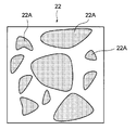
- the transfer portions 56 and 57 have an uneven structure so that the embossing 22 can be formed on the surfaces of the main body portion 12 and the covering portion 16 of the electronic device 120 as will be described later. And using the metal mold
- the transfer portions 56 and 57 cause the side surface of the main body portion 12, the bottom surface of the main body portion 12, and the surface of the covering portion 16 to be embossed as an example of “antifouling treatment”. 22 are formed.
- the texture 22 has a plurality of convex portions 22A (land portions). A shape that exhibits the effects of being hard to be damaged, difficult to get dirty, and easy to get dirty is appropriately adopted for the texture 22.
- the embossing 22 is formed on the side surface of the main body portion 12, the bottom surface of the main body portion 12, and the surface of the covering portion 16. Therefore, it is possible to suppress the side surface of the main body portion 12, the bottom surface of the main body portion 12, and the surface of the covering portion 16 from being stained by the texture 22.
- the side surface of the main body 12, the bottom surface of the main body 12, and the surface of the covering portion 16 are shown in FIG. 25 instead of the above-described emboss 22 (see FIGS. 23 and 24).
- the fine periodic structure 23 may be formed as an example of “antifouling treatment”.
- the fine periodic structure 23 is formed by changing the structure of the transfer portions 56 and 57 (see FIG. 23) of the mold 51. As shown in FIG. 26, the fine periodic structure 23 has, as an example, a plurality of fine protrusions 23A in a lattice shape.
- the arrangement pitch of the plurality of fine protrusions is preferably 5 to 20 ⁇ m.
- a shape that exhibits water repellency due to the Lotus effect or a shape that exhibits a self-cleaning action is appropriately employed. Even with such a fine periodic structure 23 having a plurality of fine protrusions, the side surface of the main body 12, the bottom surface of the main body 12, and the surface of the covering portion 16 can be suppressed.
- the embossing 22 and the fine periodic structure 23 are formed by the transfer units 56 and 57. However, after the electronic device 120 is taken out from the mold 51, the embossing 22 and the fine periodic structure 23 are added. It may be formed by work.
- the coating layer 24 having hydrophilicity and hydrophobicity may be formed.
- a coating material having hydrophilicity and hydrophobicity can be applied to the coating layer 24.
- a coating material having hydrophilicity and hydrophobicity can be applied to the coating layer 24.
- examples of such a paint include a combination of a hydrophilic acrylic polymer and a hydrophobic fluoropolymer, or a hydrophobic fluororesin with a spacing smaller than dirt particles in a hydrophilic paint. Some have fine particles dispersed. Also by such a coating layer 24, it can suppress that the side surface of the main-body part 12, the bottom face of the main-body part 12, and the surface of the coating
- the texture 22, the fine periodic structure 23, and the coating layer 24 are not formed on the surface of the covering portion 16, but are formed on the side surface of the main body portion 12 and the bottom surface of the main body portion 12. Also good. Further, the texture 22, the fine periodic structure 23, and the coating layer 24 may be formed on the surface of the covering portion 16 without being formed on the side surface of the main body portion 12 and the bottom surface of the main body portion 12. Furthermore, the texture 22, the fine periodic structure 23, and the coating layer 24 may be formed anywhere as long as they are at least a part of at least one surface of the main body 12 and the cover 16.
- the integrated module 160 includes a power generation module 161, a power storage module 162, a sensor 163, a controller 164, a memory 165, a communication circuit 166, and an antenna 167. Prepare.
- the electronic device according to the first to fourth embodiments described above is applied to the power generation module 161. That is, the power generation module 161 includes the substrate 30 (not including the communication component 32) on which the thermoelectric element 31 and the like are mounted, the main body portion 12, the heat dissipation sheet 40, and the plurality of covering portions 16 (refer to FIGS. 27).
- the power storage module 162 is connected to the power generation module 161 and stores the power generated by the power generation module 161.
- the power storage module 162 only needs to have a function of storing electric power.
- an all-solid secondary battery is preferable from the viewpoint of space saving and high safety.
- the power generation module 161 and the power storage module 162 form a power supply unit 168. Power is supplied to the sensor 163, the controller 164, and the communication circuit 166 from at least one of the power generation module 161 and the power storage module 162 that form the power supply unit 168. When stable power can be supplied by the power generation module 161, the power storage module 162 may be omitted.
- the sensor 163 is an example of a “detection unit”. As this sensor 163, for example, a sensor that detects temperature, humidity, pressure, light, sound, electromagnetic waves, acceleration, vibration, gas, fine particles, and the like can be applied. Further, the sensor 163 includes, for example, a distance measuring sensor that measures the distance to the object by emitting infrared rays to the object and receives light reflected from the object, a weight sensor that measures the weight of the object, and A water level sensor that detects data such as a water level can be applied.
- a distance measuring sensor that measures the distance to the object by emitting infrared rays to the object and receives light reflected from the object
- a weight sensor that measures the weight of the object
- a water level sensor that detects data such as a water level can be applied.
- the controller 164 transmits various data detected by the sensor 163 to the server via the communication circuit 166 and the antenna 167.
- the controller 164 may transmit secondary data based on various data detected by the sensor 163 and other data to the server.
- the controller 164 may calculate secondary data by performing predetermined calculations using various data detected by the sensor 163, and may transmit the secondary data to the server.
- the memory 165 stores various data detected by the sensor 163 and the calculated secondary data according to instructions from the controller 164.
- the stored information is read by a command from the controller 164.
- the communication circuit 166 and the antenna 167 form a communication unit 169.
- the communication unit 169 transmits and receives data between the controller 164 and a server (not shown).
- a server not shown.
- wireless communication using the antenna 167 is employed, but wired communication may be employed instead of wireless communication.
- the integrated module 160 described above is applied to an information processing system 170 according to the fifth embodiment, for example, as shown in FIG.
- the information processing system 170 includes a plurality of integrated modules 160 and a server 175.
- a plurality of integrated modules 160 are installed in the manhole 176.
- the plurality of integrated modules 160 installed in the plurality of manholes 176 are connected to the server 175 via the network 177.
- the integrated module 160 when a vehicle including the server 175 is run and the vehicle approaches the integrated module 160 installed in each manhole 176, data is transmitted from the integrated module 160 to the server 175 by short-range wireless communication. May be. Further, the integrated module 160 may be installed anywhere as long as it is a manhole 176 structure.
- the integrated module 160 is fixed to a lid 178, a concrete pipe 179, or the like, which is a structure of the manhole 176, according to the detection target of the sensor 163 or the type of the sensor 163.
- the thermoelectric element 31 provided in the integrated module 160 is thermally connected to the structure of the manhole 176 that is an example of the “object to be installed”, and the structure of the manhole 176 and the outside air or the temperature inside the manhole 176 Power is generated by the temperature difference.
- the information processing system 170 is used to grasp the deterioration of the structure of the manhole 176 (the lid 178 and the concrete pipe 179).
- the sensor 163 detects the temperature and humidity in the manhole 176, vibration (acceleration) acting on the structure of the manhole 176, and the like, and the data detected by the sensor 163 is accumulated in the memory 165.
- the controller 164 transmits the data stored in the memory 165 via the communication circuit 166 and the antenna 167.
- a server 175 provided in the measurement vehicle 180 collects data.
- the server 175 combines the position information of the vehicle 180 by the GPS (Global Positioning System) and the collected data, and displays the collected data on the map displayed on the in-vehicle monitor.
- the degree of deterioration of the concrete pipe 179 in each manhole 176 is estimated from information displaying temperature, humidity, vibration, and the like.
- a camera 182 that acquires an image of the lid 178 of the manhole 176 is attached to the lower part of the measurement vehicle 180, and deterioration of the lid 178 (iron part) of the manhole 176 is determined by image recognition. . Based on this result, the replacement time of the lid 178 of the manhole 176 may be sold as information to the local government.
- the vehicle for collecting data is not limited to a special measurement vehicle, but may be a garbage collection vehicle operated by a local government, for example. By installing the receiving device 181 and the camera 182 at the bottom of the garbage truck, data can be collected periodically without incurring collection costs.
- the sensor 163 may detect the concentration of gas generated in the manhole 176.
- An example of the gas generated in the manhole 176 is hydrogen sulfide gas. It is known that the hydrogen sulfide gas generated in the sewer 183 rapidly deteriorates the structure of the manhole 176. The generation of hydrogen sulfide gas is also a cause of complaints for neighboring residents. By using a hydrogen sulfide gas sensor as the sensor 163, the deterioration prediction accuracy of the structure of the manhole 176 can be improved, and residents' complaints can be quickly handled.
- the senor 163 may detect at least one of the temperature, humidity, vibration in the manhole 176, and the concentration of gas generated in the manhole 176.
- the humidity is always high, and there is a possibility that water from the sewer 183 (or water supply) overflows into the manhole 176.
- the inside of the manhole 176 has a substantially constant temperature.
- the lid 178 has a high temperature in summer and a low temperature in winter, and generates hydrogen sulfide gas that dissolves various metals.
- the integrated module 160 since the electronic components such as the sensor 163 and the thermoelectric element 31 are sealed with resin, long-term reliability can be maintained.
- the information processing system 170 is used to predict the flow rate of the sewer 183 connected to the manhole 176.
- a water level meter or a flow meter is used as the sensor 163.
- the sensor 163 is incorporated in the integrated module 160.
- a sensor control unit that controls the operation of an external sensor may be provided.
- the sensor control unit may control a sensor (not shown) such as a water level meter or a flow meter arranged in the sewer 183 and acquire information detected by the sensor. Information detected by the sensor may be transmitted to the sensor control unit wirelessly.
- the flow rate of the sewer 183 is detected by the sensor 163 once a day or once an hour, and the data detected by the sensor 163 is transmitted to the server 175 of the data center 184 through a high-speed communication line. Collected.
- the flow rate data of the sewer 183 detected by the sensor 163 may be transmitted simultaneously with the measurement, or may be transmitted after accumulating for one day or one week in order to reduce power consumption. .
- the measurement vehicle may collect the data.
- the prediction of the flow rate of the sewer 183 is strongly linked to the rain data. For this reason, by combining the flow rate data of the sewer 183 collected by the sensor 163 and the rainfall data of the Japan Meteorological Agency, for example, it provides flood prediction, warning information / warning information of the river into which the water of the sewer 183 flows. be able to.
- the relationship between the meteorological phenomenon and the flow rate of the sewer 183 can be established from the analysis result of the flow rate data of the sewer 183 and the rainfall data of the Japan Meteorological Agency. Then, the flow rate of the sewer 183 in each place may be predicted from the rainfall data of the Japan Meteorological Agency, and it may be charged for providing and distributing this prediction data. Since the flow rate of the sewer 183 changes from year to year according to the residential building, living conditions, and land development conditions, the information processing system 170 capable of continuous data update is useful.
- the information processing system 170 can also be used for measuring the flow rate of the sewer 183 when a localized heavy rain occurs.
- a local heavy rain in the city it is necessary to measure the water level of the sewer 183 and transmit information in minutes in order to ensure the safety of the workers of the sewer 183 and prevent the flood of the sewer 183.
- data is collected only for the integrated module 160 installed in a small number of manholes 176 having a relatively low altitude.
- the power storage module 162 of the integrated module 160 for measuring the water level is sufficiently charged in advance.
- the controller 164 sequentially transmits data to the server 175 through the communication circuit 166 and the high-speed communication line.
- the server 175 can alert the received data to a worker or a resident's smartphone or tablet near the flood.
- a measurement vehicle may be parked on a specific manhole 176, and data may be collected in a server provided in the vehicle by short-range wireless communication.
- the information processing system 170 is used for security and work history of the manhole 176.
- the sensor 163 detects opening / closing of the lid 178 of the manhole 176.
- an acceleration sensor or an open / close switch is used as this sensor 163, for example, an acceleration sensor or an open / close switch is used.
- the sensor 163 may detect at least one of acceleration generated in the lid 178 of the manhole 176 and an open / closed state of the lid 178 of the manhole 176 in order to detect the opening / closing of the lid 178 of the manhole 176.
- Data (signal) output from the sensor 163 in response to opening / closing of the lid 178 of the manhole 176 is received by the server 175.
- the information processing system 170 it is possible to check the security history of the sewer 183 and the like (for example, anti-bomb terrorism) and the work history in the cleaning work of the sewer 183.
- the information processing system 170 is used to acquire road traffic information.
- Sensor 163 detects vehicles 185, 186 and 187 passing over manhole 176.
- this sensor 163 for example, an acceleration sensor, a magnetic sensor, a microphone, or the like is used.
- a signal corresponding to the number of vehicles passing over the manhole 176 is obtained from the sensor 163.
- Data (signal) output from the sensor 163 is received by the server 175.
- this information processing system 170 it is possible to obtain traffic jam information even on narrow roads and alleys that are not measured by the current road traffic information communication system. This makes it possible to provide detailed traffic information.
- the type of the vehicles 185, 186, 187 passing through the manhole 176 may be detected from the strength of the detection value of the sensor 163.
- a data set in which the detection value of the sensor 163 is associated with the type of vehicle is stored in the memory 165 in advance. From the controller 164, information on the vehicle type determined from the detection value of the sensor 163 and the data set is transmitted to the server 175. As a result, the type of vehicle passing over the manhole 176 can be grasped.
- the individual identification information of the vehicles 185, 186, 187 passing over the manhole 176 may be detected by the sensor 163.
- the characteristics of the vehicle may be obtained by the reaction of the magnetic sensor. That is, for example, each vehicle can be identified by mounting a medium that generates a characteristic magnetism for each vehicle on the vehicle. Analyzing the difference in the flow of cars in the city depending on the type of car leads to urban road control and evaluation, such as planning to guide a specific vehicle to a specific road.
- the senor 163 may detect at least one of the number, type, and individual identification information of the vehicles passing over the manhole 176.
- the information processing system 170 is used for rainfall measurement.
- the sensor 163 for example, an X-band radar for weather prediction is used.
- the radio wave of the X-band radar does not reach the tip of the heavy rain area, for example, during heavy rain, and cannot exceed a large object such as a mountain. Also, with current radars, it is often difficult to find and track heavy rain areas that suddenly occur or develop rapidly. High-precision prediction requires high temporal and spatial resolution.
- the resolution of X-band radar is 250 m, but by installing sensor 163 in manhole 176 with an average interval of about 30 m, much finer weather observation is possible, and measurement of local torrential rain, etc. It seems to be useful for prediction.
- Data (signal) output from the sensor 163 is received by the server 175.
- the dedicated server 175 is used.
- a general-purpose computer may be used as the server 175.
- a program for executing the operations performed by the controller 164 and the server 175 may be installed and executed in a general-purpose computer that functions as the server 175.
- the program may be supplied on a recording medium or downloaded from a network.
Priority Applications (4)
| Application Number | Priority Date | Filing Date | Title |
|---|---|---|---|
| EP14880107.9A EP3098844A4 (en) | 2014-01-21 | 2014-07-08 | Heat-dissipating member, method for manufacturing heat-dissipating member, electronic device, method for manufacturing electronic device, integrated module, and information processing system |
| JP2015558723A JP6202108B2 (ja) | 2014-01-21 | 2014-07-08 | 放熱部品、放熱部品の製造方法、電子装置、電子装置の製造方法、一体型モジュール、情報処理システム |
| CN201480075879.4A CN106062948B (zh) | 2014-01-21 | 2014-07-08 | 散热部件、散热部件的制造方法、电子装置、电子装置的制造方法、集成模块以及信息处理系统 |
| US15/215,174 US10537044B2 (en) | 2014-01-21 | 2016-07-20 | Heat dissipating component, manufacturing method for heat dissipating component, electronic device, manufacturing method for electronic device, integrated module, and information processing system |
Applications Claiming Priority (2)
| Application Number | Priority Date | Filing Date | Title |
|---|---|---|---|
| JP2014-008950 | 2014-01-21 | ||
| JP2014008950 | 2014-01-21 |
Related Child Applications (1)
| Application Number | Title | Priority Date | Filing Date |
|---|---|---|---|
| US15/215,174 Continuation US10537044B2 (en) | 2014-01-21 | 2016-07-20 | Heat dissipating component, manufacturing method for heat dissipating component, electronic device, manufacturing method for electronic device, integrated module, and information processing system |
Publications (1)
| Publication Number | Publication Date |
|---|---|
| WO2015111242A1 true WO2015111242A1 (ja) | 2015-07-30 |
Family
ID=53681065
Family Applications (1)
| Application Number | Title | Priority Date | Filing Date |
|---|---|---|---|
| PCT/JP2014/068227 WO2015111242A1 (ja) | 2014-01-21 | 2014-07-08 | 放熱部品、放熱部品の製造方法、電子装置、電子装置の製造方法、一体型モジュール、情報処理システム |
Country Status (5)
| Country | Link |
|---|---|
| US (1) | US10537044B2 (zh) |
| EP (1) | EP3098844A4 (zh) |
| JP (1) | JP6202108B2 (zh) |
| CN (1) | CN106062948B (zh) |
| WO (1) | WO2015111242A1 (zh) |
Cited By (5)
| Publication number | Priority date | Publication date | Assignee | Title |
|---|---|---|---|---|
| CN106211718A (zh) * | 2016-08-23 | 2016-12-07 | 无锡金鑫集团股份有限公司 | 一种新型散热器的散热片结构 |
| US20170110386A1 (en) * | 2014-07-10 | 2017-04-20 | Fujitsu Limited | Heat dissipating component, manufacturing method for heat dissipating component, electronic device, manufacturing method for electronic device, integrated module, and information processing system |
| FR3059466A1 (fr) * | 2016-11-30 | 2018-06-01 | Sagemcom Broadband Sas | Dispositif d'evacuation de chaleur |
| US10596618B2 (en) | 2016-08-24 | 2020-03-24 | Toyota Jidosha Kabushiki Kaisha | Method for producing heat sink |
| US10950520B2 (en) * | 2018-11-22 | 2021-03-16 | Siliconware Precision Industries Co., Ltd. | Electronic package, method for fabricating the same, and heat dissipator |
Families Citing this family (7)
| Publication number | Priority date | Publication date | Assignee | Title |
|---|---|---|---|---|
| JP2016157785A (ja) * | 2015-02-24 | 2016-09-01 | 株式会社東芝 | テンプレート形成方法、テンプレートおよびテンプレート基材 |
| CN106449403B (zh) * | 2016-11-22 | 2019-06-28 | 青岛佳恩半导体有限公司 | 一种大功率igbt器件的制造方法 |
| JP6760487B2 (ja) * | 2017-03-31 | 2020-09-23 | 株式会社村田製作所 | モジュール |
| JP6787263B2 (ja) * | 2017-07-10 | 2020-11-18 | トヨタ自動車株式会社 | 電源装置 |
| US10986756B2 (en) * | 2017-12-28 | 2021-04-20 | Hughes Network Systems Llc | Cooling apparatus for an electrical component |
| KR102126773B1 (ko) * | 2018-05-15 | 2020-06-25 | 주식회사 위츠 | 무선 충전용 방열 부재 및 이를 구비하는 전자 기기 |
| TWI774008B (zh) | 2020-06-19 | 2022-08-11 | 啟碁科技股份有限公司 | 封裝結構及其製造方法 |
Citations (8)
| Publication number | Priority date | Publication date | Assignee | Title |
|---|---|---|---|---|
| JPH01201941A (ja) * | 1988-02-05 | 1989-08-14 | Citizen Watch Co Ltd | 樹脂封止型半導体装置及びその製造方法 |
| JPH05326762A (ja) | 1992-05-20 | 1993-12-10 | Ibiden Co Ltd | 半導体素子搭載装置用放熱板 |
| JPH077110A (ja) | 1993-06-16 | 1995-01-10 | Hitachi Ltd | 半導体装置 |
| JP2002314013A (ja) * | 2001-04-13 | 2002-10-25 | Hitachi Cable Ltd | 放熱材およびその製造方法 |
| JP2006024948A (ja) * | 2005-07-08 | 2006-01-26 | Nec Corp | 放熱構造、パッケージ組立体、及び放熱用シート |
| JP2009152537A (ja) | 2007-08-17 | 2009-07-09 | Shinshu Univ | 高効率放熱ヒートシンクおよびそれを用いた産業機器、電子機器、コンピューター製品および自動車 |
| JP2011222706A (ja) * | 2010-04-08 | 2011-11-04 | Canon Inc | 半導体パッケージ |
| WO2013103009A1 (ja) * | 2012-01-05 | 2013-07-11 | 富士通株式会社 | 発電装置 |
Family Cites Families (18)
| Publication number | Priority date | Publication date | Assignee | Title |
|---|---|---|---|---|
| US5233225A (en) | 1988-02-05 | 1993-08-03 | Citizen Watch Co., Ltd. | Resin encapsulated pin grid array and method of manufacturing the same |
| US5179039A (en) | 1988-02-05 | 1993-01-12 | Citizen Watch Co., Ltd. | Method of making a resin encapsulated pin grid array with integral heatsink |
| US5289039A (en) | 1988-02-05 | 1994-02-22 | Citizen Watch Co., Ltd. | Resin encapsulated semiconductor device |
| US5108955A (en) | 1988-10-27 | 1992-04-28 | Citizen Watch Co., Ltd. | Method of making a resin encapsulated pin grid array with integral heatsink |
| US5200809A (en) * | 1991-09-27 | 1993-04-06 | Vlsi Technology, Inc. | Exposed die-attach heatsink package |
| US6208513B1 (en) * | 1995-01-17 | 2001-03-27 | Compaq Computer Corporation | Independently mounted cooling fins for a low-stress semiconductor package |
| AU7096696A (en) * | 1995-11-28 | 1997-06-19 | Hitachi Limited | Semiconductor device, process for producing the same, and packaged substrate |
| US5934079A (en) * | 1997-09-09 | 1999-08-10 | Samsung Electronics Co., Ltd. | Base station heat management system |
| TW418511B (en) * | 1998-10-12 | 2001-01-11 | Siliconware Precision Industries Co Ltd | Packaged device of exposed heat sink |
| US6408935B1 (en) * | 2000-08-16 | 2002-06-25 | Thermal Corp. | Heat sink assembly with over-molded cooling fins |
| US6735450B1 (en) * | 2000-11-16 | 2004-05-11 | Symbol Technologies, Inc. | Method and apparatus for wireless outdoor environment communications networks |
| US20020195228A1 (en) * | 2001-06-07 | 2002-12-26 | International Business Machines Corporation | Thermal enhanced extended surface tape for integrated circuit heat dissipation |
| US7537151B2 (en) * | 2004-01-21 | 2009-05-26 | Delphi Technologies, Inc. | Method of making high performance heat sinks |
| US20060118969A1 (en) * | 2004-12-03 | 2006-06-08 | Taiwan Semiconductor Manufacturing Co., Ltd. | Flip chip ball grid array package assemblies and electronic devices with heat dissipation capability |
| CN101296564B (zh) * | 2007-04-27 | 2010-11-10 | 富士迈半导体精密工业(上海)有限公司 | 具良好散热性能的光源模组 |
| US7934888B2 (en) * | 2008-01-18 | 2011-05-03 | Viv Suppression, Inc. | Marine anti-foulant system and methods for using same |
| TWI404177B (zh) * | 2008-06-12 | 2013-08-01 | Mitsubishi Electric Corp | 功率半導體電路裝置及其製造方法 |
| JP5779813B2 (ja) | 2010-09-21 | 2015-09-16 | 国立大学法人岩手大学 | 金型、その製造方法、金型を用いた樹脂成形体の製造方法並びにその製造方法によって製造された樹脂成形体 |
-
2014
- 2014-07-08 WO PCT/JP2014/068227 patent/WO2015111242A1/ja active Application Filing
- 2014-07-08 JP JP2015558723A patent/JP6202108B2/ja not_active Expired - Fee Related
- 2014-07-08 CN CN201480075879.4A patent/CN106062948B/zh not_active Expired - Fee Related
- 2014-07-08 EP EP14880107.9A patent/EP3098844A4/en not_active Withdrawn
-
2016
- 2016-07-20 US US15/215,174 patent/US10537044B2/en not_active Expired - Fee Related
Patent Citations (8)
| Publication number | Priority date | Publication date | Assignee | Title |
|---|---|---|---|---|
| JPH01201941A (ja) * | 1988-02-05 | 1989-08-14 | Citizen Watch Co Ltd | 樹脂封止型半導体装置及びその製造方法 |
| JPH05326762A (ja) | 1992-05-20 | 1993-12-10 | Ibiden Co Ltd | 半導体素子搭載装置用放熱板 |
| JPH077110A (ja) | 1993-06-16 | 1995-01-10 | Hitachi Ltd | 半導体装置 |
| JP2002314013A (ja) * | 2001-04-13 | 2002-10-25 | Hitachi Cable Ltd | 放熱材およびその製造方法 |
| JP2006024948A (ja) * | 2005-07-08 | 2006-01-26 | Nec Corp | 放熱構造、パッケージ組立体、及び放熱用シート |
| JP2009152537A (ja) | 2007-08-17 | 2009-07-09 | Shinshu Univ | 高効率放熱ヒートシンクおよびそれを用いた産業機器、電子機器、コンピューター製品および自動車 |
| JP2011222706A (ja) * | 2010-04-08 | 2011-11-04 | Canon Inc | 半導体パッケージ |
| WO2013103009A1 (ja) * | 2012-01-05 | 2013-07-11 | 富士通株式会社 | 発電装置 |
Non-Patent Citations (1)
| Title |
|---|
| See also references of EP3098844A4 |
Cited By (9)
| Publication number | Priority date | Publication date | Assignee | Title |
|---|---|---|---|---|
| US20170110386A1 (en) * | 2014-07-10 | 2017-04-20 | Fujitsu Limited | Heat dissipating component, manufacturing method for heat dissipating component, electronic device, manufacturing method for electronic device, integrated module, and information processing system |
| CN106211718A (zh) * | 2016-08-23 | 2016-12-07 | 无锡金鑫集团股份有限公司 | 一种新型散热器的散热片结构 |
| CN106211718B (zh) * | 2016-08-23 | 2018-10-26 | 无锡金鑫集团股份有限公司 | 一种新型散热器的散热片结构 |
| US10596618B2 (en) | 2016-08-24 | 2020-03-24 | Toyota Jidosha Kabushiki Kaisha | Method for producing heat sink |
| FR3059466A1 (fr) * | 2016-11-30 | 2018-06-01 | Sagemcom Broadband Sas | Dispositif d'evacuation de chaleur |
| WO2018099729A1 (fr) * | 2016-11-30 | 2018-06-07 | Sagemcom Broadband Sas | Dispositif d'evacuation de chaleur |
| CN110024109A (zh) * | 2016-11-30 | 2019-07-16 | 萨基姆宽带联合股份公司 | 用于移除热量的装置 |
| US10665527B2 (en) | 2016-11-30 | 2020-05-26 | Sagemcom Broadband Sas | Device for removing heat |
| US10950520B2 (en) * | 2018-11-22 | 2021-03-16 | Siliconware Precision Industries Co., Ltd. | Electronic package, method for fabricating the same, and heat dissipator |
Also Published As
| Publication number | Publication date |
|---|---|
| EP3098844A4 (en) | 2017-06-07 |
| US20160338228A1 (en) | 2016-11-17 |
| US10537044B2 (en) | 2020-01-14 |
| CN106062948B (zh) | 2018-12-07 |
| EP3098844A1 (en) | 2016-11-30 |
| JP6202108B2 (ja) | 2017-09-27 |
| CN106062948A (zh) | 2016-10-26 |
| JPWO2015111242A1 (ja) | 2017-03-23 |
Similar Documents
| Publication | Publication Date | Title |
|---|---|---|
| JP6202108B2 (ja) | 放熱部品、放熱部品の製造方法、電子装置、電子装置の製造方法、一体型モジュール、情報処理システム | |
| JP6361730B2 (ja) | 電子装置、電子装置の製造方法、一体型モジュール、情報処理システム | |
| JP6358384B2 (ja) | 熱電変換モジュール、センサモジュール及び情報処理システム | |
| US10388844B2 (en) | Sensor module and manhole information collection/processing system | |
| US10777726B2 (en) | Thermoelectric conversion module, sensor module, and information processing system | |
| JP2014533351A (ja) | 耐衝撃性のある表面取付ルーフセンサー | |
| KR101775016B1 (ko) | 가변형 센서가 적용된 도로 침수 감지 시스템 | |
| JP2008170415A (ja) | 環境測定システム | |
| JP6299520B2 (ja) | 熱電変換モジュール及びその製造方法、センサモジュール及び情報処理システム | |
| JP2019161790A (ja) | 熱電変換装置、センサモジュール、及び情報処理システム | |
| JP2019125038A (ja) | 路面性状検査システム、路面性状検査方法、及び路面性状検査プログラム | |
| JP2016183456A (ja) | 太陽光発電装置、センシング装置及び情報処理システム | |
| WO2017149764A1 (ja) | 熱電変換モジュール、センサモジュール及び情報処理システム | |
| KR101163765B1 (ko) | 고정식 계중 장치 | |
| Kim et al. | Developing models for patterns of road surface temperature change using road and weather conditions | |
| KR102547585B1 (ko) | 침수심 계측 장치 | |
| CN111213188A (zh) | 用于产生警报行车道上的光滑性的信号的方法和装置 | |
| JP2019210394A (ja) | 蓄熱材、伝熱装置及びエネルギーハーベスタ | |
| Matzarakis et al. | Urban climate analysis of Freiburg–An integral assessment approach | |
| Kim et al. | Evaluation of Prediction Models for Road Surface Temperature Change Patterns using Machine Learning | |
| JP2007315850A (ja) | 融雪水量予測装置 | |
| JP2019041470A (ja) | 熱電変換モジュール、センサモジュール及び情報処理システム | |
| JP2010217092A (ja) | 溶融金属の液面高さ測定装置および測定方法 |
Legal Events
| Date | Code | Title | Description |
|---|---|---|---|
| 121 | Ep: the epo has been informed by wipo that ep was designated in this application |
Ref document number: 14880107 Country of ref document: EP Kind code of ref document: A1 |
|
| ENP | Entry into the national phase |
Ref document number: 2015558723 Country of ref document: JP Kind code of ref document: A |
|
| NENP | Non-entry into the national phase |
Ref country code: DE |
|
| REEP | Request for entry into the european phase |
Ref document number: 2014880107 Country of ref document: EP |
|
| WWE | Wipo information: entry into national phase |
Ref document number: 2014880107 Country of ref document: EP |