WO2015104965A1 - 半導体エピタキシャルウェーハの製造方法、半導体エピタキシャルウェーハ、および固体撮像素子の製造方法 - Google Patents
半導体エピタキシャルウェーハの製造方法、半導体エピタキシャルウェーハ、および固体撮像素子の製造方法 Download PDFInfo
- Publication number
- WO2015104965A1 WO2015104965A1 PCT/JP2014/083315 JP2014083315W WO2015104965A1 WO 2015104965 A1 WO2015104965 A1 WO 2015104965A1 JP 2014083315 W JP2014083315 W JP 2014083315W WO 2015104965 A1 WO2015104965 A1 WO 2015104965A1
- Authority
- WO
- WIPO (PCT)
- Prior art keywords
- semiconductor
- layer
- wafer
- epitaxial
- semiconductor wafer
- Prior art date
- Legal status (The legal status is an assumption and is not a legal conclusion. Google has not performed a legal analysis and makes no representation as to the accuracy of the status listed.)
- Ceased
Links
Images



Classifications
-
- H—ELECTRICITY
- H10—SEMICONDUCTOR DEVICES; ELECTRIC SOLID-STATE DEVICES NOT OTHERWISE PROVIDED FOR
- H10F—INORGANIC SEMICONDUCTOR DEVICES SENSITIVE TO INFRARED RADIATION, LIGHT, ELECTROMAGNETIC RADIATION OF SHORTER WAVELENGTH OR CORPUSCULAR RADIATION
- H10F39/00—Integrated devices, or assemblies of multiple devices, comprising at least one element covered by group H10F30/00, e.g. radiation detectors comprising photodiode arrays
- H10F39/011—Manufacture or treatment of image sensors covered by group H10F39/12
- H10F39/028—Manufacture or treatment of image sensors covered by group H10F39/12 performed after manufacture of the image sensors, e.g. annealing, gettering of impurities, short-circuit elimination or recrystallisation
-
- H—ELECTRICITY
- H10—SEMICONDUCTOR DEVICES; ELECTRIC SOLID-STATE DEVICES NOT OTHERWISE PROVIDED FOR
- H10F—INORGANIC SEMICONDUCTOR DEVICES SENSITIVE TO INFRARED RADIATION, LIGHT, ELECTROMAGNETIC RADIATION OF SHORTER WAVELENGTH OR CORPUSCULAR RADIATION
- H10F39/00—Integrated devices, or assemblies of multiple devices, comprising at least one element covered by group H10F30/00, e.g. radiation detectors comprising photodiode arrays
- H10F39/011—Manufacture or treatment of image sensors covered by group H10F39/12
- H10F39/016—Manufacture or treatment of image sensors covered by group H10F39/12 of thin-film-based image sensors
-
- H—ELECTRICITY
- H10—SEMICONDUCTOR DEVICES; ELECTRIC SOLID-STATE DEVICES NOT OTHERWISE PROVIDED FOR
- H10F—INORGANIC SEMICONDUCTOR DEVICES SENSITIVE TO INFRARED RADIATION, LIGHT, ELECTROMAGNETIC RADIATION OF SHORTER WAVELENGTH OR CORPUSCULAR RADIATION
- H10F39/00—Integrated devices, or assemblies of multiple devices, comprising at least one element covered by group H10F30/00, e.g. radiation detectors comprising photodiode arrays
- H10F39/011—Manufacture or treatment of image sensors covered by group H10F39/12
- H10F39/026—Wafer-level processing
-
- H—ELECTRICITY
- H10—SEMICONDUCTOR DEVICES; ELECTRIC SOLID-STATE DEVICES NOT OTHERWISE PROVIDED FOR
- H10F—INORGANIC SEMICONDUCTOR DEVICES SENSITIVE TO INFRARED RADIATION, LIGHT, ELECTROMAGNETIC RADIATION OF SHORTER WAVELENGTH OR CORPUSCULAR RADIATION
- H10F39/00—Integrated devices, or assemblies of multiple devices, comprising at least one element covered by group H10F30/00, e.g. radiation detectors comprising photodiode arrays
- H10F39/10—Integrated devices
- H10F39/12—Image sensors
- H10F39/199—Back-illuminated image sensors
-
- H—ELECTRICITY
- H10—SEMICONDUCTOR DEVICES; ELECTRIC SOLID-STATE DEVICES NOT OTHERWISE PROVIDED FOR
- H10P—GENERIC PROCESSES OR APPARATUS FOR THE MANUFACTURE OR TREATMENT OF DEVICES COVERED BY CLASS H10
- H10P30/00—Ion implantation into wafers, substrates or parts of devices
- H10P30/20—Ion implantation into wafers, substrates or parts of devices into semiconductor materials, e.g. for doping
- H10P30/224—Ion implantation into wafers, substrates or parts of devices into semiconductor materials, e.g. for doping of a cluster, e.g. using a gas cluster ion beam
-
- H—ELECTRICITY
- H10—SEMICONDUCTOR DEVICES; ELECTRIC SOLID-STATE DEVICES NOT OTHERWISE PROVIDED FOR
- H10P—GENERIC PROCESSES OR APPARATUS FOR THE MANUFACTURE OR TREATMENT OF DEVICES COVERED BY CLASS H10
- H10P36/00—Gettering within semiconductor bodies
- H10P36/03—Gettering within semiconductor bodies within silicon bodies
-
- H—ELECTRICITY
- H10—SEMICONDUCTOR DEVICES; ELECTRIC SOLID-STATE DEVICES NOT OTHERWISE PROVIDED FOR
- H10F—INORGANIC SEMICONDUCTOR DEVICES SENSITIVE TO INFRARED RADIATION, LIGHT, ELECTROMAGNETIC RADIATION OF SHORTER WAVELENGTH OR CORPUSCULAR RADIATION
- H10F39/00—Integrated devices, or assemblies of multiple devices, comprising at least one element covered by group H10F30/00, e.g. radiation detectors comprising photodiode arrays
- H10F39/10—Integrated devices
- H10F39/12—Image sensors
Definitions
- the present invention relates to a method for manufacturing a semiconductor epitaxial wafer, a semiconductor epitaxial wafer, and a method for manufacturing a solid-state imaging device.
- Metal contamination is a factor that degrades the characteristics of semiconductor devices.
- metal mixed in a semiconductor epitaxial wafer serving as the substrate of this device causes a dark current of the solid-state imaging device to increase and causes a defect called a white defect.
- the back-illuminated solid-state image sensor has a wiring layer, etc., placed below the sensor part, so that external light can be taken directly into the sensor and clearer images and videos can be taken even in dark places. In recent years, it has been widely used in mobile phones such as digital video cameras and smartphones. Therefore, it is desired to reduce white defect as much as possible.
- Metal contamination in the wafer mainly occurs in the manufacturing process of the semiconductor epitaxial wafer and the manufacturing process (device manufacturing process) of the solid-state imaging device.
- Metal contamination in the former semiconductor epitaxial wafer manufacturing process is caused by heavy metal particles from the components of the epitaxial growth furnace, or because the chlorine gas is used as the furnace gas during epitaxial growth, the piping material is corroded by metal. The thing by the heavy metal particle to generate
- a technique for forming a gettering site for capturing heavy metals in a semiconductor wafer there is a technique for forming a gettering site for capturing heavy metals in a semiconductor wafer.
- a method of implanting ions into a semiconductor wafer and then forming an epitaxial layer In this method, the ion implantation region functions as a gettering site.
- Patent Document 1 discloses a first step of irradiating a surface of a semiconductor wafer with cluster ions to form a modified layer in which the constituent elements of the cluster ions are dissolved on the surface of the semiconductor wafer, and the semiconductor wafer. And a second step of forming an epitaxial layer on the modified layer. A method for manufacturing a semiconductor epitaxial wafer is described.
- Patent Document 1 shows that a modified layer formed by irradiating cluster ions can obtain higher gettering ability than an ion implantation region obtained by implanting monomer ions (single ions).
- the present inventor has come to recognize the following new technical problems. That is, in order to further increase the gettering capability of the modified layer in Patent Document 1, it is effective to increase the dose of cluster ions, for example. However, it has been found that if the dose amount is increased too much, many epitaxial defects are generated in the epitaxial layer formed thereafter. In Patent Document 1, it is not considered to achieve both improvement in gettering capability and suppression of the occurrence of epitaxial defects, and there is room for improvement in this respect.
- an object of the present invention is to provide a semiconductor epitaxial wafer having high gettering ability and suppressing the occurrence of epitaxial defects, and a method for manufacturing the same.
- an amorphous region may or may not be formed in the modified layer depending on the irradiation conditions.
- a higher gettering capability can be obtained when the amorphous layer is formed in a part in the thickness direction of the modified layer than when there is no amorphous region in the modified layer. That is, in order to obtain a high gettering capability, it is necessary to irradiate cluster ions under the condition that an amorphous layer is formed in a part in the thickness direction of the modified layer.
- the manufacturing method of the semiconductor epitaxial wafer of the present invention is: A first step of irradiating the surface of the semiconductor wafer with cluster ions to form a modified layer in which the constituent elements of the cluster ions are dissolved in the surface portion of the semiconductor wafer; A second step of forming an epitaxial layer on the modified layer of the semiconductor wafer; Have In the first step, a part of the modified layer in the thickness direction is an amorphous layer, and an average depth of the surface of the amorphous layer on the surface side of the semiconductor wafer is 20 nm or more from the surface of the semiconductor wafer. It is characterized by performing.
- the first step is preferably performed such that the average depth is 20 nm or more and 200 nm or less from the surface of the semiconductor wafer.
- the first step is preferably performed so that the average thickness of the amorphous layer is 100 nm or less.
- the cluster ions preferably contain carbon as a constituent element, and more preferably contain two or more elements containing carbon as a constituent element. Moreover, it is preferable that carbon number of a cluster ion is 16 or less.
- the semiconductor epitaxial wafer of the present invention comprises a semiconductor wafer, a modified layer formed on the surface portion of the semiconductor wafer, in which a predetermined element is dissolved in the semiconductor wafer, and an epitaxial layer on the modified layer. And there is a black spot-like defect in the modified layer.
- the black spot defects are preferably present at a depth of 30 nm or more from the surface of the semiconductor wafer.
- the width of the black spot defects is preferably 30 to 100 nm, and the density of the black spot defects is preferably 1.0 ⁇ 10 8 pieces / cm 2 to 1.0 ⁇ 10 10 pieces / cm 2 .
- the predetermined element includes carbon, and it is more preferable that the predetermined element includes two or more elements including carbon.
- the solid-state imaging device manufacturing method of the present invention is characterized in that a solid-state imaging device is formed on the epitaxial layer of the semiconductor epitaxial wafer manufactured by any one of the above-described manufacturing methods or any one of the above semiconductor epitaxial wafers.
- a semiconductor epitaxial wafer having a high gettering capability and suppressing the occurrence of epitaxial defects can be obtained.
- the semiconductor epitaxial wafer of the present invention has a high gettering capability and suppresses the generation of epitaxial defects.
- FIG. 1 is a schematic cross-sectional view illustrating a method for manufacturing a semiconductor epitaxial wafer 100 according to an embodiment of the present invention.
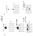
- A is a schematic diagram explaining the irradiation mechanism in the case of irradiating cluster ions
- (B) is a schematic diagram explaining the injection mechanism in the case of injecting monomer ions. The relationship between the dose amount and the average depth of the amorphous layer surface and the relationship between the dose amount and the epitaxial defect density when the acceleration voltage and the beam current value are constant using C 3 H 5 as cluster ions is shown. It is a graph.
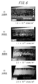
- FIG. 3 is a TEM image of a cross section of an epitaxial silicon wafer (that is, after formation of an epitaxial layer) in the experiment shown in FIG. 3, where (A) is a dose amount of 1.0 ⁇ 10 15 atoms / cm 2 (comparative example); B) is the case where the dose is 2.0 ⁇ 10 15 atoms / cm 2 (invention example), and (C) is the case where the dose is 3.0 ⁇ 10 15 atoms / cm 2 (comparative example).
- A is a dose amount of 1.0 ⁇ 10 15 atoms / cm 2 (comparative example)
- B) is the case where the dose is 2.0 ⁇ 10 15 atoms / cm 2 (invention example)
- (C) is the case where the dose is 3.0 ⁇ 10 15 atoms / cm 2 (comparative example).
- FIG. 3 is a TEM image of a cross section of an epitaxial silicon wafer (that is, after formation of an epitaxial layer) in the
- FIG. 4 is a TEM image of a cross section of a modified layer after irradiation with cluster ions and before formation of an epitaxial layer in the experiment shown in FIG. 3, where (A) shows a case where the dose is 1.0 ⁇ 10 15 atoms / cm 2 (comparative example) ), (B) when the dose is 1.7 ⁇ 10 15 atoms / cm 2 (invention example), (C) is when the dose is 2.0 ⁇ 10 15 atoms / cm 2 (invention example), (D) is a case where the dose is 3.0 ⁇ 10 15 atoms / cm 2 (comparative example).
- FIG. 1 exaggerates the thicknesses of the modified layer 14, the amorphous layer 16, and the epitaxial layer 18 with respect to the semiconductor wafer 10, unlike the actual thickness ratio.
- FIG. 1 is a schematic cross-sectional view of a semiconductor epitaxial wafer 100 obtained as a result of this manufacturing method.
- the epitaxial layer 18 becomes a device layer for manufacturing a semiconductor element such as a back-illuminated solid-state imaging element.
- Examples of the semiconductor wafer 10 include a bulk single crystal wafer made of silicon and a compound semiconductor (GaAs, GaN, SiC) and having no epitaxial layer on the surface. Specifically, a bulk single crystal silicon wafer is used. Moreover, the semiconductor wafer 10 can use what sliced the single crystal silicon ingot grown by the Czochralski method (CZ method) and the floating zone melting method (FZ method) with the wire saw etc. In order to obtain a higher gettering capability, carbon and / or nitrogen may be added to the semiconductor wafer 10. Furthermore, a predetermined concentration of an arbitrary dopant may be added to the semiconductor wafer 10 to form a so-called n + type or p + type, or n ⁇ type or p ⁇ type substrate.
- CZ method Czochralski method
- FZ method floating zone melting method
- an epitaxial semiconductor wafer in which a semiconductor epitaxial layer is formed on the surface of the bulk semiconductor wafer may be used.
- the silicon epitaxial layer can be formed under general conditions by a CVD method.
- the epitaxial layer preferably has a thickness in the range of 0.1 to 10 ⁇ m, and more preferably in the range of 0.2 to 5 ⁇ m.
- the modified layer 14 formed as a result of irradiating the cluster ions 12 is a region where the constituent elements of the cluster ions 12 are locally present as a solid solution at the interstitial positions or substitution positions of crystals on the surface of the semiconductor wafer. Work as a gettering site. The reason is presumed as follows. That is, elements such as carbon irradiated in the form of cluster ions are localized at a high density at the substitution position / interstitial position of the silicon single crystal.
- cluster ions mean ions that are ionized by applying a positive charge or a negative charge to a cluster formed by aggregating a plurality of atoms or molecules.
- a cluster is a massive group in which a plurality (usually about 2 to 2000) of atoms or molecules are bonded to each other.
- the cluster ions 12 are irradiated in the present embodiment, a higher gettering ability can be obtained as compared with the case of injecting monomer ions.
- the present inventor considers an operation that can obtain such an effect as follows.
- the monomer ions are implanted into a silicon wafer, as shown in FIG. 2B, the monomer ions are blown off silicon atoms constituting the silicon wafer and implanted at a predetermined depth in the silicon wafer.
- the implantation depth depends on the type of constituent elements of the implanted ions and the acceleration voltage of the ions.
- the concentration profile of carbon in the depth direction of the silicon wafer is relatively broad, and the region where the implanted carbon is present is approximately 0.5 to 1 ⁇ m.
- lighter elements are implanted deeper, that is, implanted at different positions according to the mass of each element, so the concentration profile of the implanted elements becomes broader. .
- the cluster ions 12 are instantaneously 1350 to 1400 with the energy when irradiated to the silicon wafer. It becomes a high temperature of about °C and silicon melts. Thereafter, the silicon is rapidly cooled, and carbon and hydrogen are dissolved in the vicinity of the surface in the silicon wafer. That is, the “modified layer” in the present specification means a layer in which constituent elements of irradiated ions are dissolved in crystal interstitial positions or substitution positions on the surface of the semiconductor wafer.
- the concentration profile of carbon in the depth direction of the silicon wafer depends on the acceleration voltage and cluster size of cluster ions, but is sharper than that of monomer ions, and is a locally existing region of irradiated carbon (ie,
- the modified layer has a thickness of about 500 nm or less (for example, about 50 to 400 nm). Note that the elements irradiated in the form of cluster ions undergo some thermal diffusion during the formation process of the epitaxial layer 18. For this reason, in the carbon concentration profile after the formation of the epitaxial layer 18, broad diffusion regions are formed on both sides of the peak where these elements exist locally. However, the thickness of the modified layer (that is, the peak width) does not change greatly. As a result, the carbon deposition region can be locally and highly concentrated.
- the modified layer 14 is formed in the vicinity of the surface of the silicon wafer, that is, immediately below the epitaxial layer 18, proximity gettering is possible. As a result, it is considered that high gettering ability can be obtained. In addition, if it is a form of cluster ion, you may irradiate multiple types of ion simultaneously.
- a part of the modified layer 14 in the thickness direction becomes the amorphous layer 16, and the average depth of the surface 16A of the amorphous layer 16 on the semiconductor wafer surface side is Irradiation of cluster ions is performed so as to be 20 nm or more from the semiconductor wafer surface 10A.
- the amorphous layer 16 is present in the modified layer 14, the gettering capability of the modified layer 14 described above can be obtained more sufficiently. Therefore, the back-illuminated solid-state imaging device manufactured from the semiconductor epitaxial wafer 100 obtained according to the present embodiment can be expected to suppress the occurrence of white defect.
- the average depth of the surface 16A of the amorphous layer 16 is 20 nm or more from the semiconductor wafer surface 10A, the generation of epitaxial defects in the epitaxial layer 18 to be formed thereafter can be sufficiently suppressed.
- the average depth of the surface 16A of the amorphous layer 16 is preferably 20 nm or more and 200 nm or less from the semiconductor wafer surface 10A, and is preferably 20 nm or more and 80 nm or less. More preferably.
- the average thickness of the amorphous layer 16 is preferably 100 nm or less, and more preferably 60 nm or less. This is because if it exceeds 100 nm, it may be difficult to select cluster irradiation conditions for setting the average depth of the surface 16A to 20 nm or more from the semiconductor wafer surface 10A.
- the surface of the amorphous layer varies in depth depending on the position in the lateral direction.
- the “average depth of the surface on the wafer surface side” is defined by the average depth of the surface in the TEM image obtained by observing the cross section of the amorphous layer with a transmission electron microscope (TEM).
- the “average depth” is a depth intermediate between the shallowest position and the deepest position of the boundary line between the amorphous layer and the crystal region.
- the “average thickness of the amorphous layer” is also defined by the average thickness of the amorphous layer in the TEM image, that is, the difference between the average depths of the two surfaces of the amorphous layer.
- the magnification of the TEM image only needs to be such that the amorphous layer can be clearly observed. In the example shown in FIG.
- the cluster ion has various clusters depending on the binding mode, and can be generated by a known method as described in the following document, for example.
- a method for generating a gas cluster beam (1) JP-A-9-41138, (2) JP-A-4-354865, and as an ion beam generation method, (1) charged particle beam engineering: Junzo Ishikawa: ISBN978 -4-339-00734-3: Corona, (2) Electron / ion beam engineering: The Institute of Electrical Engineers of Japan: ISBN4-88686-217-9: Ohm, (3) Cluster ion beam foundation and application: ISBN4-526-05765 -7: Nikkan Kogyo Shimbun.
- a Nielsen ion source or a Kaufman ion source is used to generate positively charged cluster ions
- a large current negative ion source using a volume generation method is used to generate negatively charged cluster ions. It is done.
- the irradiated element is not particularly limited as long as it contributes to gettering, and examples thereof include carbon, boron, phosphorus, and arsenic.
- the cluster ions preferably contain carbon as a constituent element. Since the carbon atom at the lattice position has a smaller covalent bond radius than that of the silicon single crystal, a contraction field of the silicon crystal lattice is formed, so that the gettering ability to attract impurities between the lattices is high.
- the irradiation element two or more elements including carbon are more preferable.
- dopant elements selected from the group consisting of boron, phosphorus, arsenic and antimony in addition to carbon.
- a compound to be ionized is not particularly limited, and ethane, methane, carbon dioxide (CO 2 ), or the like can be used as a carbon source compound that can be ionized, and diborane, decaborane ( B 10 H 14 ) or the like can be used.
- diborane, decaborane ( B 10 H 14 ) or the like can be used.
- a gas obtained by mixing dibenzyl and decaborane is used as a material gas
- a hydrogen compound cluster in which carbon, boron and hydrogen are aggregated can be generated.
- cyclohexane (C 6 H 12 ) is used as a material gas
- cluster ions composed of carbon and hydrogen can be generated.
- the carbon source compound it is particularly preferable to use a cluster C n H m (3 ⁇ n ⁇ 16, 3 ⁇ m ⁇ 10) formed from pyrene (C 16 H 10 ), dibenzyl (C 14 H 14 ) or the like. This is because it is easy to control a small-sized cluster ion beam.
- the compound to be ionized is also preferably a compound containing both carbon and the above dopant element. This is because if such a compound is irradiated as cluster ions, both carbon and the dopant element can be dissolved in a single irradiation.
- cluster size means the number of atoms or molecules constituting one cluster.
- the cluster size can be appropriately set to 2 to 100, preferably 60 or less, more preferably 50 or less. In the examples described later, C 3 H 5 having 8 cluster sizes and 6 cluster sizes are used. C 3 H 3 was used.
- the cluster size can be adjusted by adjusting the gas pressure of the gas ejected from the nozzle, the pressure of the vacuum vessel, the voltage applied to the filament during ionization, and the like.
- the cluster size can be obtained by obtaining a cluster number distribution by mass spectrometry using a quadrupole high-frequency electric field or time-of-flight mass spectrometry and taking an average value of the number of clusters.
- the dose of cluster ions can be adjusted by controlling the ion irradiation time.
- the dose needs to be approximately 1 ⁇ 10 15 atoms / cm 2 or more.
- the carbon dose is 1.7 ⁇ 10 15 atoms / cm 2 or more (see FIG. 3)
- the carbon dose is Of 2.2 ⁇ 10 15 atoms / cm 2 or more (see FIG. 4)
- an amorphous layer was formed in the modified layer.
- the dose amount needs to be approximately 1 ⁇ 10 16 atoms / cm 2 or less.
- the carbon dose is 2.0 ⁇ 10 15 atoms / cm 2 or less (see FIG. 3)
- the carbon dose is Was 2.6 ⁇ 10 15 atoms / cm 2 or less (see FIG. 4)
- the average depth of the surface 16A was 20 nm or more from the semiconductor wafer surface 10A.
- the acceleration voltage of cluster ions affects the peak position of the concentration profile in the depth direction of the constituent elements in the modified layer 18 as well as the cluster size, and therefore indirectly affects the depth of the amorphous layer.
- electrostatic acceleration For adjusting the acceleration voltage, two methods of (1) electrostatic acceleration and (2) high frequency acceleration are generally used.
- As the former method there is a method in which a plurality of electrodes are arranged at equal intervals and an equal voltage is applied between them to create an equal acceleration electric field in the axial direction.
- As the latter method there is a linear linac method in which ions are accelerated using a high frequency while running linearly.
- the beam current value needs to be approximately 100 ⁇ A or more and 1000 ⁇ A or less.
- Monomer ions are generally implanted at an acceleration voltage of about 150 to 2000 keV, and each ion collides with a silicon atom with its energy. Therefore, the crystallinity of the surface of the silicon wafer into which the monomer ions are implanted is disturbed, and then the wafer surface. Disturb the crystallinity of the epitaxial layer grown on it.
- cluster ions are generally irradiated at an accelerating voltage of about 10 to 100 keV / Cluster. However, since a cluster is an aggregate of a plurality of atoms or molecules, it must be implanted with a small energy per atom or molecule. Damage to the crystal of the semiconductor wafer is small.
- the semiconductor wafer after the first step, can be transferred to an epitaxial growth apparatus and the second step can be performed without performing a heat treatment for crystallinity recovery on the semiconductor wafer.
- the semiconductor epitaxial wafer 100 having high gettering capability can be efficiently manufactured. That is, it is not necessary to perform recovery heat treatment using a rapid heating / cooling heat treatment device such as RTA (Rapid Thermal Annealing) or RTO (Rapid Thermal Oxidation) that is separate from the epitaxial device.
- RTA Rapid Thermal Annealing
- RTO Rapid Thermal Oxidation
- the crystallinity of the semiconductor wafer 10 can be sufficiently recovered by hydrogen baking performed prior to epitaxial growth in an epitaxial apparatus for forming the epitaxial layer 18 described below.
- the general conditions for the hydrogen baking process are that the inside of the epitaxial growth apparatus is in a hydrogen atmosphere, the semiconductor wafer 10 is placed in the furnace at a furnace temperature of 600 ° C. or higher and 900 ° C. or lower, and 1 ° C./second or higher and 15 ° C./second or lower. The temperature is raised to a temperature range of 1100 ° C. or higher and 1200 ° C. or lower at a temperature rising rate, and the temperature is maintained for 30 seconds or longer and 1 minute or shorter.
- This hydrogen baking process is originally intended to remove the natural oxide film formed on the wafer surface by the cleaning process before the epitaxial layer growth.
- the crystallinity of the semiconductor wafer 10 is sufficiently recovered by the hydrogen baking under the above conditions. Can be made.
- recovery heat treatment may be performed after the first step and before the second step by using a heat treatment apparatus separate from the epitaxial apparatus.
- This recovery heat treatment may be performed at 900 ° C. to 1200 ° C. for 10 seconds to 1 hour.
- This recovery heat treatment is performed using, for example, a rapid heating / cooling heat treatment apparatus such as RTA or RTO, or a batch heat treatment apparatus (vertical heat treatment apparatus, horizontal heat treatment apparatus) before the semiconductor wafer 10 is transferred into the epitaxial growth apparatus. be able to.
- Examples of the epitaxial layer 18 formed on the modified layer 14 include a silicon epitaxial layer, which can be formed under general conditions.
- a source gas such as dichlorosilane or trichlorosilane is introduced into the chamber using hydrogen as a carrier gas, and the growth temperature differs depending on the source gas used, but the semiconductor is formed by CVD at a temperature in the range of about 1000 to 1200 ° C. It can be epitaxially grown on the wafer 10.
- the epitaxial layer 18 preferably has a thickness in the range of 1 to 15 ⁇ m.
- the resistivity of the epitaxial layer 18 may change due to outdiffusion of the dopant from the semiconductor wafer 10, and if it exceeds 15 ⁇ m, the spectral sensitivity characteristics of the solid-state imaging device are affected. Because there is a fear.
- the semiconductor epitaxial wafer 100 obtained by the manufacturing method will be described.
- the semiconductor epitaxial wafer 100 includes a semiconductor wafer 10 and a modified layer 14 formed on the surface portion of the semiconductor wafer 10 in which a predetermined element is dissolved in the semiconductor wafer 10; And an epitaxial layer 18 on the modified layer 14.
- the definition of the modified layer 14 is as described above, and elemental analysis is performed in the depth direction from the surface 10A of the semiconductor wafer 10 with a SIMS (secondary ion mass spectrometer), and the concentration profile of the predetermined element in the depth direction. It can be specified as a steep peak portion.
- the modified layer 14 usually extends from the surface 10A of the semiconductor wafer 10 to a depth of 50 to 400 nm from the surface 10A.
- black spots 20 are present in the modified layer 18.
- the “black spot defect” means a defect observed as a black spot in the modified layer 14 when the cleaved cross section of the semiconductor epitaxial wafer 100 is observed in a bright mode with a TEM.
- the black spot defects are generated in the modified layer 14 after the formation of the epitaxial layer 18 only when the amorphous layer 16 is formed in the modified layer 14 after irradiation with the cluster ions 12. To do.
- no black spot defect occurs in the modified layer after the formation of the epitaxial layer.
- the mechanism of black spot defects is estimated as follows. That is, in the recrystallization process in which the amorphous layer formed in the modified layer before the epitaxial layer is recovered by receiving thermal energy during epitaxial growth, it was introduced not only by silicon atoms but also by cluster irradiation. Cluster elements (carbon atoms, etc.), oxygen atoms in silicon wafers, etc. are taken into the recrystallized region, and the recrystallized region takes the form of complex clusters and is assumed to be observed as a black spot-like defect Is done.
- the semiconductor epitaxial wafer 100 in which the black spot-like defects 20 exist has a high gettering capability.
- the average depth of the amorphous layer surface 16A is 20 nm or more from the surface 10A of the semiconductor wafer, the occurrence of epitaxial defects can be suppressed, and the thickness of the amorphous layer increases as the average depth becomes less than 20 nm.
- the present inventors have found that a line-shaped defect layer connected with black spots is formed, and that this line-shaped defect layer is the starting point and an epitaxial defect is generated.
- the epitaxial defect density of the epitaxial layer 18 is 0. .04 pieces / cm 2 or less.
- the black spot defects are preferably present at a depth of 30 nm or more from the surface of the semiconductor wafer.
- the size of the black spot defects is about 30 to 100 nm in width (wafer radial direction) and about 20 to 60 nm in height (wafer thickness direction).
- the density of black spot defects is preferably 1.0 ⁇ 10 8 pieces / cm 2 to 1.0 ⁇ 10 10 pieces / cm 2 . If it is 1.0 ⁇ 10 8 pieces / cm 2 or more, the effect of suppressing the occurrence of epitaxial defects can be sufficiently obtained. If it is 1.0 ⁇ 10 10 pieces / cm 2 or less, the line-shaped defect layer is not formed as described above.
- the predetermined element is not particularly limited as long as it is an element other than the main material of the semiconductor wafer (silicon in the case of a silicon wafer), but it is preferable to use carbon or two or more elements containing carbon as described above. It is.
- the semiconductor epitaxial wafer 100 of this embodiment has a high gettering capability and suppresses the generation of epitaxial defects.
- the method for manufacturing a solid-state imaging device includes a solid-state imaging device on the semiconductor epitaxial wafer manufactured by the manufacturing method described above or the epitaxial layer 18 positioned on the surface of the semiconductor epitaxial wafer, that is, the semiconductor epitaxial wafer 100. It is characterized by forming.
- the solid-state imaging device obtained by this manufacturing method can sufficiently suppress the occurrence of white defect as compared with the conventional case.
- Example 1 An n-type silicon wafer (diameter: 300 mm, thickness: 725 ⁇ m, dopant: phosphorus, dopant concentration: 5.0 ⁇ 10 14 atoms / cm 3 ) obtained from a CZ single crystal silicon ingot was prepared. Next, a C 3 H 5 cluster is generated from cyclohexane using a cluster ion generator (manufactured by Nissin Ion Equipment Co., Ltd., model number: CLARIS), and the carbon dose is 1.0 ⁇ 10 15 atoms / cm 2. As a result, the surface of the silicon wafer was irradiated to form a modified layer. The acceleration voltage per carbon atom was 23.4 keV / atom, and the beam current value was 400 ⁇ A.
- a cluster ion generator manufactured by Nissin Ion Equipment Co., Ltd., model number: CLARIS
- FIG. 6A shows an image obtained by observing a cross section around the modified layer after irradiation with cluster ions with a TEM.
- the amorphous layer is a portion that looks white in FIGS. 6B to 6D, and it can be seen that the amorphous layer was not formed in the modified layer of FIG.
- the silicon wafer is transferred into a single wafer epitaxial growth apparatus (Applied Materials Co., Ltd.), subjected to a hydrogen baking process at a temperature of 1120 ° C. for 30 seconds, and then hydrogen as a carrier gas and trichlorosilane as a source.
- a silicon epitaxial layer (thickness: 8 ⁇ m, dopant: phosphorus, dopant concentration: 1.0 ⁇ 10 15 atoms / cm 3 ) is epitaxially grown on the modified layer of the silicon wafer by a CVD method at 1150 ° C. as a gas. A wafer was obtained.
- the carbon and hydrogen concentration profiles were measured by SIMS measurement. Since a steep peak was confirmed in the range of 80 nm from the silicon wafer surface, the modified layer could be identified.
- the cross section around the modified layer of the silicon epitaxial wafer was observed with TEM. A black belt-like portion in the image shown in FIG. 5A is a modified layer, but no black spot-like defect was observed.
- the carbon and hydrogen concentration profiles were measured by SIMS measurement. Since a steep peak was confirmed in the range of 80 nm from the silicon wafer surface, the modified layer could be identified.
- the cross section around the modified layer of the silicon epitaxial wafer was observed.
- a black belt-like portion in the image shown in FIG. 5B is a modified layer, and black spot-like defects were observed therein.
- the inventive example showed higher gettering ability than the comparative example.
- the amorphous layer is formed in the modified layer, so that the region of the amorphous layer is recrystallized after the formation of the epitaxial layer, and the region also contributes as a gettering site.
- Example 2 As shown in the plot of FIG. 3, the same method as in Experimental Example 1 except that the carbon dose was set to a plurality of conditions from 1.0 ⁇ 10 15 atoms / cm 2 to 1.0 ⁇ 10 16 atoms / cm 2. Thus, a plurality of silicon epitaxial wafers were produced with different dose amounts.
- FIG. 6A shows a case where the dose amount is 1.0 ⁇ 10 15 atoms / cm 2
- FIG. 6B shows a case where the dose amount is 1.7 ⁇ 10 15 atoms / cm 2
- FIG. 6C shows the case where the dose amount is 2.0 ⁇ 10 15 atoms / cm 2
- FIG. 6A shows a case where the dose amount is 1.0 ⁇ 10 15 atoms / cm 2
- FIG. 6B shows a case where the dose amount is 1.7 ⁇ 10 15 atoms / cm 2
- FIG. 6C shows the case where the dose amount is 2.0 ⁇ 10 15 atoms / cm 2
- FIG. 6D shows the case where the dose amount is 3.0 ⁇ 10 15 atoms / cm 2 .
- the average depth of the surface of the amorphous layer on the semiconductor wafer surface was 55 nm in FIG. 6B, 20 nm in FIG. 6C, and 5 nm in FIG. 6D.
- the average thickness of the amorphous layer was 5 nm in FIG. 6 (B), 30 nm in FIG. 6 (C), and 60 nm in FIG. 6 (D).
- FIG. 3 shows the relationship between the dose and the average depth.
- the dose amount was less than 1.7 ⁇ 10 15 atoms / cm 2
- the average depth was 20 nm or more in a dose range of 1.7 ⁇ 10 15 atoms / cm 2 or more and 2.0 ⁇ 10 15 atoms / cm 2 or less.
- FIG. 3 shows the relationship between the dose and the epitaxial defect density. When the dose amount exceeded 2.0 ⁇ 10 15 atoms / cm 2 , epitaxial defects exceeding 0.04 pieces / cm 2 occurred.
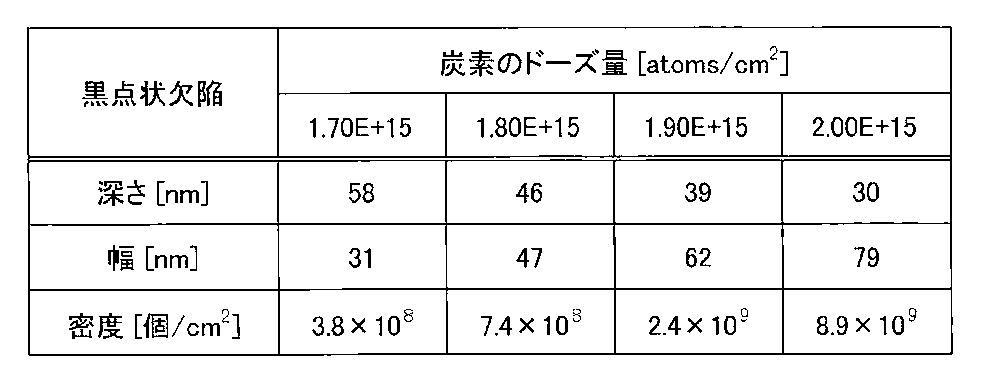
- the dose amount is 1.7 ⁇ 10 15 atoms / cm 2 or more and 2.0 ⁇ 10 15 atoms / cm 2 or less, as shown in FIG. Black spots were observed. When the dose was less than 1.7 ⁇ 10 15 atoms / cm 2 , no black spot defects were observed. When the dose amount exceeds 2.0 ⁇ 10 15 atoms / cm 2 , black spot defects are not observed, and as shown in FIG. 5C, a line-shaped defect layer in which black spots are connected is representative. Observed.
- Table 2 shows the depth of the black spot defects from the surface of the silicon wafer and the width and density of the black spot defects under the four experimental conditions in which the black spot defects were observed.
- Example 3 The same experiment as in Experimental Example 2 was performed except that the cluster ion species was a C 3 H 3 cluster generated from cyclohexane, and the result of FIG. 4 was obtained.
- an amorphous layer is formed with a dose amount of 2.2 ⁇ 10 15 atoms / cm 2 or more and high gettering ability is obtained, while a dose amount is 2.6 ⁇ 10 15 atoms / cm 2 or less.
- the average depth was 20 nm or more, and the generation of epitaxial defects could be sufficiently suppressed.
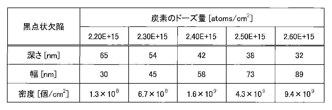
- the dose amount is 2.2 ⁇ 10 15 atoms / cm 2 or more and 2.6 ⁇ 10 15 atoms / cm 2 or less.
- black spot-like defects were observed after the formation of the epitaxial layer.
- the dose was less than 2.2 ⁇ 10 15 atoms / cm 2 .
- no black spot defects were observed.
- the dose amount exceeded 2.6 ⁇ 10 15 atoms / cm 2 , no black spot defects were observed, and a line defect layer in which black spots were connected was observed.
- Table 3 shows the depth of the black spot defects from the surface of the silicon wafer and the width and density of the black spot defects under the five experimental conditions in which the black spot defects were observed.
- the present invention it is possible to provide a semiconductor epitaxial wafer having high gettering capability and suppressing generation of defects in the epitaxial layer, and a method for manufacturing the same.
Landscapes
- Recrystallisation Techniques (AREA)
- Chemical & Material Sciences (AREA)
- Engineering & Computer Science (AREA)
- Materials Engineering (AREA)
- Nanotechnology (AREA)
- Solid State Image Pick-Up Elements (AREA)
Abstract
Description
(1)半導体ウェーハにクラスターイオンを照射した場合、照射条件によって、改質層中にアモルファス領域が形成される場合と形成されない場合とがあった。そして、改質層中にアモルファス領域がない場合よりも、改質層の厚み方向の一部にアモルファス層が形成される場合の方が、高いゲッタリング能力を得ることができた。すなわち、高いゲッタリング能力を得るためには、改質層の厚み方向の一部にアモルファス層が形成される条件で、クラスターイオンを照射する必要がある。
すなわち、本発明の半導体エピタキシャルウェーハの製造方法は、
半導体ウェーハの表面にクラスターイオンを照射して、該半導体ウェーハの表面部に、前記クラスターイオンの構成元素が固溶した改質層を形成する第1工程と、
前記半導体ウェーハの改質層上にエピタキシャル層を形成する第2工程と、
を有し、
前記第1工程は、前記改質層における厚み方向の一部がアモルファス層となり、かつ、該アモルファス層の前記半導体ウェーハ表面側の表面の平均深さが前記半導体ウェーハ表面から20nm以上となるように行うことを特徴とする。
本発明の一実施形態による半導体エピタキシャルウェーハ100の製造方法は、図1に示すように、半導体ウェーハ10の表面10Aにクラスターイオン12を照射して、半導体ウェーハ10の表面部に、このクラスターイオン12の構成元素が固溶した改質層14を形成する第1工程(図1(A),(B))と、半導体ウェーハ10の改質層14上にエピタキシャル層18を形成する第2工程(図1(C))と、を有する。図1(C)は、この製造方法の結果得られた半導体エピタキシャルウェーハ100の模式断面図である。エピタキシャル層18は、裏面照射型固体撮像素子等の半導体素子を製造するためのデバイス層となる。
次に、上記製造方法により得られる半導体エピタキシャルウェーハ100について説明する。半導体エピタキシャルウェーハ100は、図1(C)に示すように、半導体ウェーハ10と、この半導体ウェーハ10の表面部に形成された、半導体ウェーハ10中に所定元素が固溶した改質層14と、この改質層14上のエピタキシャル層18と、を有する。
本発明の実施形態による固体撮像素子の製造方法は、上記の製造方法で製造された半導体エピタキシャルウェーハまたは上記の半導体エピタキシャルウェーハ、すなわち半導体エピタキシャルウェーハ100の表面に位置するエピタキシャル層18に、固体撮像素子を形成することを特徴とする。この製造方法により得られる固体撮像素子は、従来に比べ白傷欠陥の発生を十分に抑制することができる。
(比較例)
CZ単結晶シリコンインゴットから得たn型シリコンウェーハ(直径:300mm、厚さ:725μm、ドーパント:リン、ドーパント濃度:5.0×10¹⁴atoms/cm3)を用意した。次に、クラスターイオン発生装置(日新イオン機器社製、型番:CLARIS)を用いて、シクロヘキサンよりC3H5クラスターを生成して、炭素のドーズ量を1.0×1015atoms/cm2として、シリコンウェーハの表面に照射し、改質層を形成した。炭素1原子当りの加速電圧は23.4keV/atom、ビーム電流値は400μAとした。
炭素のドーズ量を2.0×10¹⁵atoms/cm2とした以外は、上記比較例と同じ実験を行った。クラスターイオン照射後の改質層周辺の断面をTEMにて観察した。図6(C)に示すように、改質層中にアモルファス層が形成されていた。図中、白く見える部分がアモルファス層である。
比較例および発明例で作製したシリコンエピタキシャルウェーハの表面を、Ni汚染液およびFe汚染液(ともに1.2×10¹³/cm2)で、それぞれスピンコート汚染法を用いて故意に汚染し、引き続き900℃、30分の熱処理を施した。その後、SIMS測定を行い、改質層に捕獲されたNiおよびFeの濃度を測定した。結果を表1に示す。

炭素のドーズ量を図3のプロットに示すように、1.0×10¹⁵atoms/cm2から1.0×1016atoms/cm2までの複数条件とした以外は、実験例1と同じ方法で、それぞれ異なるドーズ量で複数枚のシリコンエピタキシャルウェーハを作製した。
クラスターイオン種を、シクロヘキサンより生成したC3H3クラスターとした以外は、実験例2と同じ実験を行い、図4の結果を得た。この場合は、ドーズ量が2.2×10¹⁵atoms/cm2以上でアモルファス層は形成され、高いゲッタリング能力が得られ、一方で、ドーズ量が2.6×1015atoms/cm2以下で、平均深さが20nm以上となり、エピタキシャル欠陥の発生を十分に抑制できることがわかった。
10 半導体ウェーハ
10A 半導体ウェーハの表面
12 クラスターイオン
14 改質層
16 アモルファス層
16A アモルファス層の半導体ウェーハ表面側の表面
18 エピタキシャル層
20 黒点状欠陥
Claims (12)
- 半導体ウェーハの表面にクラスターイオンを照射して、該半導体ウェーハの表面部に、前記クラスターイオンの構成元素が固溶した改質層を形成する第1工程と、
前記半導体ウェーハの改質層上にエピタキシャル層を形成する第2工程と、
を有し、
前記第1工程は、前記改質層における厚み方向の一部がアモルファス層となり、かつ、該アモルファス層の前記半導体ウェーハ表面側の表面の平均深さが前記半導体ウェーハ表面から20nm以上となるように行うことを特徴とする半導体エピタキシャルウェーハの製造方法。 - 前記第1工程は、前記平均深さが前記半導体ウェーハ表面から20nm以上200nm以下となるように行う請求項1に記載の半導体エピタキシャルウェーハの製造方法。
- 前記第1工程は、前記アモルファス層の平均厚さが100nm以下となるように行う請求項1または2に記載の半導体エピタキシャルウェーハの製造方法。
- 前記クラスターイオンが、構成元素として炭素を含む請求項1~3のいずれか1項に記載の半導体エピタキシャルウェーハの製造方法。
- 前記クラスターイオンが、構成元素として炭素を含む2種以上の元素を含む請求項4に記載の半導体エピタキシャルウェーハの製造方法。
- 前記クラスターイオンの炭素数が16個以下である請求項4または5に記載の半導体エピタキシャルウェーハの製造方法。
- 半導体ウェーハと、該半導体ウェーハの表面部に形成された、該半導体ウェーハ中に所定元素が固溶した改質層と、該改質層上のエピタキシャル層と、を有し、
前記改質層に黒点状欠陥が存在することを特徴とする半導体エピタキシャルウェーハ。 - 前記黒点状欠陥が前記半導体ウェーハの表面から30nm以上の深さに存在する請求項7に記載の半導体エピタキシャルウェーハ。
- 前記黒点状欠陥の幅が30~100nmであり、前記黒点状欠陥の密度が1.0×10⁸個/cm2~1.0×1010個/cm2である請求項7または8に記載の半導体エピタキシャルウェーハ。
- 前記所定元素が炭素を含む請求項7~9のいずれか1項に記載の半導体エピタキシャルウェーハ。
- 前記所定元素が炭素を含む2種以上の元素を含む請求項10に記載の半導体エピタキシャルウェーハ。
- 請求項1~6のいずれか1項に記載の製造方法で製造された半導体エピタキシャルウェーハまたは請求項7~11のいずれか1項に記載の半導体エピタキシャルウェーハの、前記エピタキシャル層に、固体撮像素子を形成することを特徴とする固体撮像素子の製造方法。
Priority Applications (7)
| Application Number | Priority Date | Filing Date | Title |
|---|---|---|---|
| US15/104,396 US10153323B2 (en) | 2014-01-07 | 2014-12-10 | Method of producing semiconductor epitaxial wafer, semiconductor epitaxial wafer, and method of producing solid-state image sensor |
| CN201480068832.5A CN105814671B (zh) | 2014-01-07 | 2014-12-10 | 半导体外延晶片的制造方法、半导体外延晶片、以及固体摄像元件的制造方法 |
| KR1020177013854A KR101882389B1 (ko) | 2014-01-07 | 2014-12-10 | 반도체 에피택셜 웨이퍼의 제조방법, 반도체 에피택셜 웨이퍼, 및 고체 촬상 소자의 제조방법 |
| DE112014005494.1T DE112014005494T5 (de) | 2014-01-07 | 2014-12-10 | Verfahren zur Herstellung eines Halbleiter-Epitaxialwafers, ein Halbleiter-Epitaxialwafer und Verfahren zur Herstellung eines Festkörperbildsensors |
| KR1020167016695A KR20160078515A (ko) | 2014-01-07 | 2014-12-10 | 반도체 에피택셜 웨이퍼의 제조방법, 반도체 에피택셜 웨이퍼, 및 고체 촬상 소자의 제조방법 |
| US16/139,505 US10629648B2 (en) | 2014-01-07 | 2018-09-24 | Method of producing semiconductor epitaxial wafer, semiconductor epitaxial wafer, and method of producing solid-state image sensor |
| US16/816,883 US11211423B2 (en) | 2014-01-07 | 2020-03-12 | Method of producing semiconductor epitaxial wafer, semiconductor epitaxial wafer, and method of producing solid-state image sensor |
Applications Claiming Priority (2)
| Application Number | Priority Date | Filing Date | Title |
|---|---|---|---|
| JP2014-001182 | 2014-01-07 | ||
| JP2014001182A JP6065848B2 (ja) | 2014-01-07 | 2014-01-07 | 半導体エピタキシャルウェーハの製造方法、半導体エピタキシャルウェーハ、および固体撮像素子の製造方法 |
Related Child Applications (2)
| Application Number | Title | Priority Date | Filing Date |
|---|---|---|---|
| US15/104,396 A-371-Of-International US10153323B2 (en) | 2014-01-07 | 2014-12-10 | Method of producing semiconductor epitaxial wafer, semiconductor epitaxial wafer, and method of producing solid-state image sensor |
| US16/139,505 Continuation US10629648B2 (en) | 2014-01-07 | 2018-09-24 | Method of producing semiconductor epitaxial wafer, semiconductor epitaxial wafer, and method of producing solid-state image sensor |
Publications (1)
| Publication Number | Publication Date |
|---|---|
| WO2015104965A1 true WO2015104965A1 (ja) | 2015-07-16 |
Family
ID=53523803
Family Applications (1)
| Application Number | Title | Priority Date | Filing Date |
|---|---|---|---|
| PCT/JP2014/083315 Ceased WO2015104965A1 (ja) | 2014-01-07 | 2014-12-10 | 半導体エピタキシャルウェーハの製造方法、半導体エピタキシャルウェーハ、および固体撮像素子の製造方法 |
Country Status (7)
| Country | Link |
|---|---|
| US (3) | US10153323B2 (ja) |
| JP (1) | JP6065848B2 (ja) |
| KR (2) | KR20160078515A (ja) |
| CN (2) | CN107452603B (ja) |
| DE (1) | DE112014005494T5 (ja) |
| TW (1) | TWI539044B (ja) |
| WO (1) | WO2015104965A1 (ja) |
Cited By (6)
| Publication number | Priority date | Publication date | Assignee | Title |
|---|---|---|---|---|
| WO2016031328A1 (ja) * | 2014-08-28 | 2016-03-03 | 株式会社Sumco | 半導体エピタキシャルウェーハおよびその製造方法、ならびに、固体撮像素子の製造方法 |
| WO2016104080A1 (ja) * | 2014-12-25 | 2016-06-30 | 株式会社Sumco | 半導体エピタキシャルウェーハの製造方法および固体撮像素子の製造方法 |
| WO2017145470A1 (ja) * | 2016-02-25 | 2017-08-31 | 株式会社Sumco | エピタキシャルウェーハの製造方法およびエピタキシャルウェーハ |
| KR20190108612A (ko) | 2017-02-28 | 2019-09-24 | 가부시키가이샤 사무코 | 에피택셜 실리콘 웨이퍼의 불순물 게터링 능력의 평가 방법 및 에피택셜 실리콘 웨이퍼 |
| JPWO2022044562A1 (ja) * | 2020-08-26 | 2022-03-03 | ||
| KR20250133738A (ko) | 2023-02-22 | 2025-09-08 | 가부시키가이샤 사무코 | 에피택셜 실리콘 웨이퍼 및 그 제조 방법, 그리고 반도체 디바이스의 제조 방법 |
Families Citing this family (12)
| Publication number | Priority date | Publication date | Assignee | Title |
|---|---|---|---|---|
| JP6737066B2 (ja) | 2016-08-22 | 2020-08-05 | 株式会社Sumco | エピタキシャルシリコンウェーハの製造方法、エピタキシャルシリコンウェーハ、及び固体撮像素子の製造方法 |
| JP6729447B2 (ja) * | 2017-02-24 | 2020-07-22 | 株式会社Sumco | エピタキシャルシリコンウェーハの製造方法および固体撮像素子の製造方法 |
| JP6380582B1 (ja) * | 2017-03-08 | 2018-08-29 | 株式会社Sumco | エピタキシャルウェーハの裏面検査方法、エピタキシャルウェーハ裏面検査装置、エピタキシャル成長装置のリフトピン管理方法およびエピタキシャルウェーハの製造方法 |
| JP6891655B2 (ja) * | 2017-06-14 | 2021-06-18 | 株式会社Sumco | 半導体ウェーハの製造方法および半導体ウェーハ |
| JP6772966B2 (ja) * | 2017-06-14 | 2020-10-21 | 株式会社Sumco | エピタキシャル成長用の半導体ウェーハの製造方法及び半導体エピタキシャルウェーハの製造方法 |
| JP6784237B2 (ja) * | 2017-07-14 | 2020-11-11 | 信越半導体株式会社 | シリコンエピタキシャルウェーハの製造方法 |
| JP6787268B2 (ja) * | 2017-07-20 | 2020-11-18 | 株式会社Sumco | 半導体エピタキシャルウェーハおよびその製造方法、ならびに固体撮像素子の製造方法 |
| JP6801682B2 (ja) * | 2018-02-27 | 2020-12-16 | 株式会社Sumco | 半導体エピタキシャルウェーハの製造方法及び半導体デバイスの製造方法 |
| JP6930459B2 (ja) * | 2018-03-01 | 2021-09-01 | 株式会社Sumco | 半導体エピタキシャルウェーハの製造方法 |
| JP6874718B2 (ja) * | 2018-03-01 | 2021-05-19 | 株式会社Sumco | 半導体エピタキシャルウェーハの製造方法 |
| JP7043899B2 (ja) * | 2018-03-08 | 2022-03-30 | 株式会社Sumco | 半導体ウェーハのゲッタリング能力評価方法 |
| JP7088239B2 (ja) * | 2020-08-20 | 2022-06-21 | 株式会社Sumco | エピタキシャル成長用の半導体ウェーハ、および半導体エピタキシャルウェーハの製造方法 |
Citations (4)
| Publication number | Priority date | Publication date | Assignee | Title |
|---|---|---|---|---|
| JP2007317760A (ja) * | 2006-05-24 | 2007-12-06 | Sharp Corp | 半導体装置及びその製造方法 |
| JP2010040864A (ja) * | 2008-08-06 | 2010-02-18 | Sumco Corp | エピタキシャルシリコンウェーハ及びその製造方法 |
| JP2011253983A (ja) * | 2010-06-03 | 2011-12-15 | Disco Abrasive Syst Ltd | シリコンウェーハへのゲッタリング層付与方法 |
| WO2012157162A1 (ja) * | 2011-05-13 | 2012-11-22 | 株式会社Sumco | 半導体エピタキシャルウェーハの製造方法、半導体エピタキシャルウェーハ、および固体撮像素子の製造方法 |
Family Cites Families (14)
| Publication number | Priority date | Publication date | Assignee | Title |
|---|---|---|---|---|
| JPH04130731A (ja) * | 1990-09-21 | 1992-05-01 | Hitachi Ltd | 半導体集積回路装置の製造方法 |
| JP2002368001A (ja) | 2001-06-07 | 2002-12-20 | Denso Corp | 半導体装置及びその製造方法 |
| JP2003163216A (ja) * | 2001-09-12 | 2003-06-06 | Wacker Nsce Corp | エピタキシャルシリコンウエハおよびその製造方法 |
| AU2003228587A1 (en) * | 2002-04-18 | 2003-11-03 | University Of Florida | Biomimetic organic/inorganic composites, processes for their production, and methods of use |
| JP4519592B2 (ja) * | 2004-09-24 | 2010-08-04 | 株式会社東芝 | 非水電解質二次電池用負極活物質及び非水電解質二次電池 |
| EP1874443A4 (en) * | 2005-04-29 | 2009-09-16 | Univ Rochester | ULTRA-THAN POROUS NANOSCAL MEMBRANES, MANUFACTURING METHOD AND USES THEREOF |
| DE102005024073A1 (de) * | 2005-05-25 | 2006-11-30 | Siltronic Ag | Halbleiter-Schichtstruktur und Verfahren zur Herstellung einer Halbleiter-Schichtstruktur |
| KR101455404B1 (ko) | 2005-12-09 | 2014-10-27 | 세미이큅, 인코포레이티드 | 탄소 클러스터의 주입에 의한 반도체 디바이스의 제조를위한 시스템 및 방법 |
| JP5204959B2 (ja) * | 2006-06-26 | 2013-06-05 | 株式会社半導体エネルギー研究所 | 半導体装置の作製方法 |
| JP2010062529A (ja) * | 2008-08-04 | 2010-03-18 | Toshiba Corp | 半導体装置の製造方法 |
| JP5580010B2 (ja) * | 2008-09-05 | 2014-08-27 | 株式会社半導体エネルギー研究所 | 半導体装置の作製方法 |
| WO2011125305A1 (ja) | 2010-04-08 | 2011-10-13 | 信越半導体株式会社 | シリコンエピタキシャルウエーハ、シリコンエピタキシャルウエーハの製造方法、及び半導体素子又は集積回路の製造方法 |
| CN103180030B (zh) * | 2010-08-23 | 2017-04-12 | 艾克索乔纳斯公司 | 基于气体团簇离子束技术的中性射束处理方法和设备 |
| WO2013149014A1 (en) * | 2012-03-29 | 2013-10-03 | Wayne State University | Bimetal catalysts |
-
2014
- 2014-01-07 JP JP2014001182A patent/JP6065848B2/ja active Active
- 2014-12-10 CN CN201710594191.2A patent/CN107452603B/zh active Active
- 2014-12-10 WO PCT/JP2014/083315 patent/WO2015104965A1/ja not_active Ceased
- 2014-12-10 KR KR1020167016695A patent/KR20160078515A/ko not_active Ceased
- 2014-12-10 CN CN201480068832.5A patent/CN105814671B/zh active Active
- 2014-12-10 DE DE112014005494.1T patent/DE112014005494T5/de active Pending
- 2014-12-10 KR KR1020177013854A patent/KR101882389B1/ko active Active
- 2014-12-10 US US15/104,396 patent/US10153323B2/en active Active
-
2015
- 2015-01-05 TW TW104100005A patent/TWI539044B/zh active
-
2018
- 2018-09-24 US US16/139,505 patent/US10629648B2/en active Active
-
2020
- 2020-03-12 US US16/816,883 patent/US11211423B2/en active Active
Patent Citations (4)
| Publication number | Priority date | Publication date | Assignee | Title |
|---|---|---|---|---|
| JP2007317760A (ja) * | 2006-05-24 | 2007-12-06 | Sharp Corp | 半導体装置及びその製造方法 |
| JP2010040864A (ja) * | 2008-08-06 | 2010-02-18 | Sumco Corp | エピタキシャルシリコンウェーハ及びその製造方法 |
| JP2011253983A (ja) * | 2010-06-03 | 2011-12-15 | Disco Abrasive Syst Ltd | シリコンウェーハへのゲッタリング層付与方法 |
| WO2012157162A1 (ja) * | 2011-05-13 | 2012-11-22 | 株式会社Sumco | 半導体エピタキシャルウェーハの製造方法、半導体エピタキシャルウェーハ、および固体撮像素子の製造方法 |
Cited By (15)
| Publication number | Priority date | Publication date | Assignee | Title |
|---|---|---|---|---|
| WO2016031328A1 (ja) * | 2014-08-28 | 2016-03-03 | 株式会社Sumco | 半導体エピタキシャルウェーハおよびその製造方法、ならびに、固体撮像素子の製造方法 |
| JP2016051729A (ja) * | 2014-08-28 | 2016-04-11 | 株式会社Sumco | 半導体エピタキシャルウェーハおよびその製造方法、ならびに、固体撮像素子の製造方法 |
| WO2016104080A1 (ja) * | 2014-12-25 | 2016-06-30 | 株式会社Sumco | 半導体エピタキシャルウェーハの製造方法および固体撮像素子の製造方法 |
| US10224203B2 (en) | 2014-12-25 | 2019-03-05 | Sumco Corporation | Method of producing semiconductor epitaxial wafer and method of producing solid-state image sensor |
| WO2017145470A1 (ja) * | 2016-02-25 | 2017-08-31 | 株式会社Sumco | エピタキシャルウェーハの製造方法およびエピタキシャルウェーハ |
| US10861709B2 (en) | 2017-02-28 | 2020-12-08 | Sumco Corporation | Method of evaluating impurity gettering capability of epitaxial silicon wafer and epitaxial silicon wafer |
| KR20190108612A (ko) | 2017-02-28 | 2019-09-24 | 가부시키가이샤 사무코 | 에피택셜 실리콘 웨이퍼의 불순물 게터링 능력의 평가 방법 및 에피택셜 실리콘 웨이퍼 |
| JPWO2022044562A1 (ja) * | 2020-08-26 | 2022-03-03 | ||
| WO2022044562A1 (ja) * | 2020-08-26 | 2022-03-03 | 株式会社Sumco | エピタキシャルシリコンウェーハ及びその製造方法、並びに半導体デバイスの製造方法 |
| TWI784671B (zh) * | 2020-08-26 | 2022-11-21 | 日商Sumco股份有限公司 | 磊晶矽晶圓及其製造方法、以及半導體元件的製造方法 |
| KR20230044229A (ko) | 2020-08-26 | 2023-04-03 | 가부시키가이샤 사무코 | 에피택셜 실리콘 웨이퍼 및 그 제조 방법, 그리고 반도체 디바이스의 제조 방법 |
| DE112021004491T5 (de) | 2020-08-26 | 2023-07-06 | Sumco Corporation | Epitaktischer siliziumwafer und verfahren zu dessen herstellung sowie verfahren zur herstellung eines halbleiterbauelements |
| JP7416270B2 (ja) | 2020-08-26 | 2024-01-17 | 株式会社Sumco | エピタキシャルシリコンウェーハ及びその製造方法、並びに半導体デバイスの製造方法 |
| US12414388B2 (en) | 2020-08-26 | 2025-09-09 | Sumco Corporation | Epitaxial silicon wafer, method for producing same, and method for producing semiconductor device |
| KR20250133738A (ko) | 2023-02-22 | 2025-09-08 | 가부시키가이샤 사무코 | 에피택셜 실리콘 웨이퍼 및 그 제조 방법, 그리고 반도체 디바이스의 제조 방법 |
Also Published As
| Publication number | Publication date |
|---|---|
| JP2015130402A (ja) | 2015-07-16 |
| CN105814671B (zh) | 2019-03-29 |
| KR20170059020A (ko) | 2017-05-29 |
| CN107452603A (zh) | 2017-12-08 |
| DE112014005494T5 (de) | 2016-09-15 |
| US10629648B2 (en) | 2020-04-21 |
| CN105814671A (zh) | 2016-07-27 |
| CN107452603B (zh) | 2020-12-18 |
| TWI539044B (zh) | 2016-06-21 |
| US11211423B2 (en) | 2021-12-28 |
| JP6065848B2 (ja) | 2017-01-25 |
| KR20160078515A (ko) | 2016-07-04 |
| US20160315117A1 (en) | 2016-10-27 |
| US20190027533A1 (en) | 2019-01-24 |
| KR101882389B1 (ko) | 2018-07-26 |
| US10153323B2 (en) | 2018-12-11 |
| TW201531600A (zh) | 2015-08-16 |
| US20200219929A1 (en) | 2020-07-09 |
Similar Documents
| Publication | Publication Date | Title |
|---|---|---|
| JP6065848B2 (ja) | 半導体エピタキシャルウェーハの製造方法、半導体エピタキシャルウェーハ、および固体撮像素子の製造方法 | |
| JP5673811B2 (ja) | 半導体エピタキシャルウェーハの製造方法、半導体エピタキシャルウェーハ、および固体撮像素子の製造方法 | |
| JP5799936B2 (ja) | 半導体エピタキシャルウェーハの製造方法、半導体エピタキシャルウェーハ、および固体撮像素子の製造方法 | |
| CN107134404A (zh) | 半导体外延晶片和其制造方法以及固体摄像元件的制造方法 | |
| JP6107068B2 (ja) | エピタキシャルシリコンウェーハの製造方法、エピタキシャルシリコンウェーハ、および固体撮像素子の製造方法 | |
| TWI611482B (zh) | 半導體磊晶晶圓的製造方法及固體攝像元件的製造方法 | |
| JP6427946B2 (ja) | エピタキシャルシリコンウェーハの製造方法、エピタキシャルシリコンウェーハ、および固体撮像素子の製造方法 | |
| JP6221928B2 (ja) | 半導体エピタキシャルウェーハの製造方法および固体撮像素子の製造方法 | |
| JP6508030B2 (ja) | シリコンエピタキシャルウェーハの製造方法および固体撮像素子の製造方法 | |
| JP2014099457A (ja) | 半導体エピタキシャルウェーハの製造方法、半導体エピタキシャルウェーハ、および固体撮像素子の製造方法 | |
| JP6280301B2 (ja) | エピタキシャルシリコンウェーハの製造方法、エピタキシャルシリコンウェーハ、および固体撮像素子の製造方法 | |
| JP6289805B2 (ja) | 半導体エピタキシャルウェーハの製造方法、半導体エピタキシャルウェーハ、および固体撮像素子の製造方法 | |
| JP6278592B2 (ja) | 半導体エピタキシャルウェーハの製造方法、半導体エピタキシャルウェーハ、および固体撮像素子の製造方法 | |
| JP2015220242A (ja) | 半導体エピタキシャルウェーハの製造方法および固体撮像素子の製造方法 | |
| JP6318728B2 (ja) | 半導体エピタキシャルウェーハの製造方法、半導体エピタキシャルウェーハ、および固体撮像素子の製造方法 | |
| JP6361779B2 (ja) | エピタキシャルシリコンウェーハの製造方法、エピタキシャルシリコンウェーハ、および固体撮像素子の製造方法 | |
| JP2017175143A (ja) | 半導体エピタキシャルウェーハの製造方法、半導体エピタキシャルウェーハ、および固体撮像素子の製造方法 | |
| JP2017183736A (ja) | 半導体エピタキシャルウェーハの製造方法、半導体エピタキシャルウェーハ、および固体撮像素子の製造方法 |
Legal Events
| Date | Code | Title | Description |
|---|---|---|---|
| WWE | Wipo information: entry into national phase |
Ref document number: 112014005494 Country of ref document: DE |
|
| 121 | Ep: the epo has been informed by wipo that ep was designated in this application |
Ref document number: 14877788 Country of ref document: EP Kind code of ref document: A1 |
|
| WWE | Wipo information: entry into national phase |
Ref document number: 15104396 Country of ref document: US |
|
| ENP | Entry into the national phase |
Ref document number: 20167016695 Country of ref document: KR Kind code of ref document: A |
|
| 122 | Ep: pct application non-entry in european phase |
Ref document number: 14877788 Country of ref document: EP Kind code of ref document: A1 |