JP5799936B2 - 半導体エピタキシャルウェーハの製造方法、半導体エピタキシャルウェーハ、および固体撮像素子の製造方法 - Google Patents
半導体エピタキシャルウェーハの製造方法、半導体エピタキシャルウェーハ、および固体撮像素子の製造方法 Download PDFInfo
- Publication number
- JP5799936B2 JP5799936B2 JP2012249731A JP2012249731A JP5799936B2 JP 5799936 B2 JP5799936 B2 JP 5799936B2 JP 2012249731 A JP2012249731 A JP 2012249731A JP 2012249731 A JP2012249731 A JP 2012249731A JP 5799936 B2 JP5799936 B2 JP 5799936B2
- Authority
- JP
- Japan
- Prior art keywords
- wafer
- semiconductor
- epitaxial
- layer
- carbon
- Prior art date
- Legal status (The legal status is an assumption and is not a legal conclusion. Google has not performed a legal analysis and makes no representation as to the accuracy of the status listed.)
- Active
Links
- 239000004065 semiconductor Substances 0.000 title claims description 127
- 238000004519 manufacturing process Methods 0.000 title claims description 44
- 238000003384 imaging method Methods 0.000 title claims description 18
- 150000002500 ions Chemical class 0.000 claims description 106
- 239000002019 doping agent Substances 0.000 claims description 97
- XUIMIQQOPSSXEZ-UHFFFAOYSA-N Silicon Chemical group [Si] XUIMIQQOPSSXEZ-UHFFFAOYSA-N 0.000 claims description 87
- 229910052710 silicon Inorganic materials 0.000 claims description 86
- 239000010703 silicon Substances 0.000 claims description 85
- 229910052799 carbon Inorganic materials 0.000 claims description 79
- OKTJSMMVPCPJKN-UHFFFAOYSA-N Carbon Chemical compound [C] OKTJSMMVPCPJKN-UHFFFAOYSA-N 0.000 claims description 73
- ZOXJGFHDIHLPTG-UHFFFAOYSA-N Boron Chemical compound [B] ZOXJGFHDIHLPTG-UHFFFAOYSA-N 0.000 claims description 31
- 229910052796 boron Inorganic materials 0.000 claims description 31
- 238000010438 heat treatment Methods 0.000 claims description 30
- 229910052698 phosphorus Inorganic materials 0.000 claims description 18
- OAICVXFJPJFONN-UHFFFAOYSA-N Phosphorus Chemical compound [P] OAICVXFJPJFONN-UHFFFAOYSA-N 0.000 claims description 17
- 239000011574 phosphorus Substances 0.000 claims description 17
- 150000001875 compounds Chemical class 0.000 claims description 16
- 239000000470 constituent Substances 0.000 claims description 15
- 238000011084 recovery Methods 0.000 claims description 11
- 229910052785 arsenic Inorganic materials 0.000 claims description 8
- RQNWIZPPADIBDY-UHFFFAOYSA-N arsenic atom Chemical compound [As] RQNWIZPPADIBDY-UHFFFAOYSA-N 0.000 claims description 8
- 230000001678 irradiating effect Effects 0.000 claims description 8
- 229910052787 antimony Inorganic materials 0.000 claims description 7
- WATWJIUSRGPENY-UHFFFAOYSA-N antimony atom Chemical compound [Sb] WATWJIUSRGPENY-UHFFFAOYSA-N 0.000 claims description 7
- 238000002407 reforming Methods 0.000 claims description 3
- 235000012431 wafers Nutrition 0.000 description 164
- 125000004429 atom Chemical group 0.000 description 74
- 238000000034 method Methods 0.000 description 48
- 238000005247 gettering Methods 0.000 description 38
- 239000000178 monomer Substances 0.000 description 31
- 230000001133 acceleration Effects 0.000 description 27
- 239000007789 gas Substances 0.000 description 27
- 238000011109 contamination Methods 0.000 description 16
- 239000000463 material Substances 0.000 description 16
- 229910052751 metal Inorganic materials 0.000 description 16
- 239000002184 metal Substances 0.000 description 16
- 230000008569 process Effects 0.000 description 14
- 230000000052 comparative effect Effects 0.000 description 13
- 238000001004 secondary ion mass spectrometry Methods 0.000 description 13
- 239000013078 crystal Substances 0.000 description 11
- 238000005468 ion implantation Methods 0.000 description 11
- 239000001257 hydrogen Substances 0.000 description 10
- 229910052739 hydrogen Inorganic materials 0.000 description 10
- 238000005259 measurement Methods 0.000 description 10
- YWWDBCBWQNCYNR-UHFFFAOYSA-N trimethylphosphine Chemical compound CP(C)C YWWDBCBWQNCYNR-UHFFFAOYSA-N 0.000 description 10
- QVGXLLKOCUKJST-UHFFFAOYSA-N atomic oxygen Chemical compound [O] QVGXLLKOCUKJST-UHFFFAOYSA-N 0.000 description 9
- 230000007547 defect Effects 0.000 description 9
- 239000001301 oxygen Substances 0.000 description 9
- 229910052760 oxygen Inorganic materials 0.000 description 9
- 239000000758 substrate Substances 0.000 description 9
- UFHFLCQGNIYNRP-UHFFFAOYSA-N Hydrogen Chemical compound [H][H] UFHFLCQGNIYNRP-UHFFFAOYSA-N 0.000 description 8
- 229910001385 heavy metal Inorganic materials 0.000 description 8
- 238000009792 diffusion process Methods 0.000 description 7
- 238000011156 evaluation Methods 0.000 description 7
- 238000004140 cleaning Methods 0.000 description 6
- PXHVJJICTQNCMI-UHFFFAOYSA-N Nickel Chemical compound [Ni] PXHVJJICTQNCMI-UHFFFAOYSA-N 0.000 description 5
- 239000010949 copper Substances 0.000 description 5
- 229910021421 monocrystalline silicon Inorganic materials 0.000 description 5
- XYFCBTPGUUZFHI-UHFFFAOYSA-N Phosphine Chemical compound P XYFCBTPGUUZFHI-UHFFFAOYSA-N 0.000 description 4
- 150000001721 carbon Chemical group 0.000 description 4
- 229910052802 copper Inorganic materials 0.000 description 4
- 230000001747 exhibiting effect Effects 0.000 description 4
- 230000009471 action Effects 0.000 description 3
- 230000015572 biosynthetic process Effects 0.000 description 3
- -1 carbon ions Chemical class 0.000 description 3
- 230000008859 change Effects 0.000 description 3
- 230000000694 effects Effects 0.000 description 3
- 238000002513 implantation Methods 0.000 description 3
- 239000012535 impurity Substances 0.000 description 3
- 238000010884 ion-beam technique Methods 0.000 description 3
- 230000007246 mechanism Effects 0.000 description 3
- 229910052759 nickel Inorganic materials 0.000 description 3
- 239000007787 solid Substances 0.000 description 3
- 239000006104 solid solution Substances 0.000 description 3
- 238000006467 substitution reaction Methods 0.000 description 3
- WXRGABKACDFXMG-UHFFFAOYSA-N trimethylborane Chemical compound CB(C)C WXRGABKACDFXMG-UHFFFAOYSA-N 0.000 description 3
- IJGRMHOSHXDMSA-UHFFFAOYSA-N Atomic nitrogen Chemical compound N#N IJGRMHOSHXDMSA-UHFFFAOYSA-N 0.000 description 2
- CURLTUGMZLYLDI-UHFFFAOYSA-N Carbon dioxide Chemical compound O=C=O CURLTUGMZLYLDI-UHFFFAOYSA-N 0.000 description 2
- 229940032122 claris Drugs 0.000 description 2
- 238000001816 cooling Methods 0.000 description 2
- 238000010586 diagram Methods 0.000 description 2
- 238000009826 distribution Methods 0.000 description 2
- 230000005684 electric field Effects 0.000 description 2
- 238000005530 etching Methods 0.000 description 2
- 238000002474 experimental method Methods 0.000 description 2
- 239000007788 liquid Substances 0.000 description 2
- 239000002923 metal particle Substances 0.000 description 2
- 150000002739 metals Chemical class 0.000 description 2
- VNWKTOKETHGBQD-UHFFFAOYSA-N methane Chemical compound C VNWKTOKETHGBQD-UHFFFAOYSA-N 0.000 description 2
- 238000005498 polishing Methods 0.000 description 2
- 239000002244 precipitate Substances 0.000 description 2
- 238000001556 precipitation Methods 0.000 description 2
- IHCDKJZZFOUARO-UHFFFAOYSA-M sulfacetamide sodium Chemical compound O.[Na+].CC(=O)[N-]S(=O)(=O)C1=CC=C(N)C=C1 IHCDKJZZFOUARO-UHFFFAOYSA-M 0.000 description 2
- ZDHXKXAHOVTTAH-UHFFFAOYSA-N trichlorosilane Chemical compound Cl[SiH](Cl)Cl ZDHXKXAHOVTTAH-UHFFFAOYSA-N 0.000 description 2
- 239000005052 trichlorosilane Substances 0.000 description 2
- RIOQSEWOXXDEQQ-UHFFFAOYSA-N triphenylphosphine Chemical compound C1=CC=CC=C1P(C=1C=CC=CC=1)C1=CC=CC=C1 RIOQSEWOXXDEQQ-UHFFFAOYSA-N 0.000 description 2
- QWUWMCYKGHVNAV-UHFFFAOYSA-N 1,2-dihydrostilbene Chemical group C=1C=CC=CC=1CCC1=CC=CC=C1 QWUWMCYKGHVNAV-UHFFFAOYSA-N 0.000 description 1
- DJMUYABFXCIYSC-UHFFFAOYSA-N 1H-phosphole Chemical compound C=1C=CPC=1 DJMUYABFXCIYSC-UHFFFAOYSA-N 0.000 description 1
- 229910052580 B4C Inorganic materials 0.000 description 1
- KZBUYRJDOAKODT-UHFFFAOYSA-N Chlorine Chemical compound ClCl KZBUYRJDOAKODT-UHFFFAOYSA-N 0.000 description 1
- RYGMFSIKBFXOCR-UHFFFAOYSA-N Copper Chemical compound [Cu] RYGMFSIKBFXOCR-UHFFFAOYSA-N 0.000 description 1
- XDTMQSROBMDMFD-UHFFFAOYSA-N Cyclohexane Chemical compound C1CCCCC1 XDTMQSROBMDMFD-UHFFFAOYSA-N 0.000 description 1
- OTMSDBZUPAUEDD-UHFFFAOYSA-N Ethane Chemical compound CC OTMSDBZUPAUEDD-UHFFFAOYSA-N 0.000 description 1
- 229910001218 Gallium arsenide Inorganic materials 0.000 description 1
- VYPSYNLAJGMNEJ-UHFFFAOYSA-N Silicium dioxide Chemical compound O=[Si]=O VYPSYNLAJGMNEJ-UHFFFAOYSA-N 0.000 description 1
- 230000002411 adverse Effects 0.000 description 1
- 229910052782 aluminium Inorganic materials 0.000 description 1
- XAGFODPZIPBFFR-UHFFFAOYSA-N aluminium Chemical compound [Al] XAGFODPZIPBFFR-UHFFFAOYSA-N 0.000 description 1
- 125000001797 benzyl group Chemical group [H]C1=C([H])C([H])=C(C([H])=C1[H])C([H])([H])* 0.000 description 1
- INAHAJYZKVIDIZ-UHFFFAOYSA-N boron carbide Chemical compound B12B3B4C32B41 INAHAJYZKVIDIZ-UHFFFAOYSA-N 0.000 description 1
- 229910052795 boron group element Inorganic materials 0.000 description 1
- 229910002092 carbon dioxide Inorganic materials 0.000 description 1
- 239000001569 carbon dioxide Substances 0.000 description 1
- 239000012159 carrier gas Substances 0.000 description 1
- 238000005229 chemical vapour deposition Methods 0.000 description 1
- 229910052804 chromium Inorganic materials 0.000 description 1
- 230000008602 contraction Effects 0.000 description 1
- 230000007797 corrosion Effects 0.000 description 1
- 238000005260 corrosion Methods 0.000 description 1
- 238000013461 design Methods 0.000 description 1
- MROCJMGDEKINLD-UHFFFAOYSA-N dichlorosilane Chemical compound Cl[SiH2]Cl MROCJMGDEKINLD-UHFFFAOYSA-N 0.000 description 1
- 238000010894 electron beam technology Methods 0.000 description 1
- BHEPBYXIRTUNPN-UHFFFAOYSA-N hydridophosphorus(.) (triplet) Chemical compound [PH] BHEPBYXIRTUNPN-UHFFFAOYSA-N 0.000 description 1
- 150000002431 hydrogen Chemical class 0.000 description 1
- 239000007943 implant Substances 0.000 description 1
- 238000002347 injection Methods 0.000 description 1
- 239000007924 injection Substances 0.000 description 1
- 229910052742 iron Inorganic materials 0.000 description 1
- 238000004949 mass spectrometry Methods 0.000 description 1
- 239000000155 melt Substances 0.000 description 1
- 238000002156 mixing Methods 0.000 description 1
- 229910052757 nitrogen Inorganic materials 0.000 description 1
- 230000003647 oxidation Effects 0.000 description 1
- 238000007254 oxidation reaction Methods 0.000 description 1
- 239000002245 particle Substances 0.000 description 1
- 125000004437 phosphorous atom Chemical group 0.000 description 1
- 229910052696 pnictogen Inorganic materials 0.000 description 1
- 239000000047 product Substances 0.000 description 1
- 230000000630 rising effect Effects 0.000 description 1
- 230000035945 sensitivity Effects 0.000 description 1
- 229910052814 silicon oxide Inorganic materials 0.000 description 1
- 230000003595 spectral effect Effects 0.000 description 1
- 230000001629 suppression Effects 0.000 description 1
- 230000002195 synergetic effect Effects 0.000 description 1
- 238000001269 time-of-flight mass spectrometry Methods 0.000 description 1
- 229910052723 transition metal Inorganic materials 0.000 description 1
- 150000003624 transition metals Chemical class 0.000 description 1
- LALRXNPLTWZJIJ-UHFFFAOYSA-N triethylborane Chemical compound CCB(CC)CC LALRXNPLTWZJIJ-UHFFFAOYSA-N 0.000 description 1
- 238000004857 zone melting Methods 0.000 description 1
Images


Classifications
-
- H—ELECTRICITY
- H01—ELECTRIC ELEMENTS
- H01L—SEMICONDUCTOR DEVICES NOT COVERED BY CLASS H10
- H01L27/00—Devices consisting of a plurality of semiconductor or other solid-state components formed in or on a common substrate
- H01L27/14—Devices consisting of a plurality of semiconductor or other solid-state components formed in or on a common substrate including semiconductor components sensitive to infrared radiation, light, electromagnetic radiation of shorter wavelength or corpuscular radiation and specially adapted either for the conversion of the energy of such radiation into electrical energy or for the control of electrical energy by such radiation
- H01L27/144—Devices controlled by radiation
- H01L27/146—Imager structures
- H01L27/14683—Processes or apparatus peculiar to the manufacture or treatment of these devices or parts thereof
- H01L27/14687—Wafer level processing
-
- C—CHEMISTRY; METALLURGY
- C23—COATING METALLIC MATERIAL; COATING MATERIAL WITH METALLIC MATERIAL; CHEMICAL SURFACE TREATMENT; DIFFUSION TREATMENT OF METALLIC MATERIAL; COATING BY VACUUM EVAPORATION, BY SPUTTERING, BY ION IMPLANTATION OR BY CHEMICAL VAPOUR DEPOSITION, IN GENERAL; INHIBITING CORROSION OF METALLIC MATERIAL OR INCRUSTATION IN GENERAL
- C23C—COATING METALLIC MATERIAL; COATING MATERIAL WITH METALLIC MATERIAL; SURFACE TREATMENT OF METALLIC MATERIAL BY DIFFUSION INTO THE SURFACE, BY CHEMICAL CONVERSION OR SUBSTITUTION; COATING BY VACUUM EVAPORATION, BY SPUTTERING, BY ION IMPLANTATION OR BY CHEMICAL VAPOUR DEPOSITION, IN GENERAL
- C23C14/00—Coating by vacuum evaporation, by sputtering or by ion implantation of the coating forming material
- C23C14/22—Coating by vacuum evaporation, by sputtering or by ion implantation of the coating forming material characterised by the process of coating
- C23C14/48—Ion implantation
-
- C—CHEMISTRY; METALLURGY
- C30—CRYSTAL GROWTH
- C30B—SINGLE-CRYSTAL GROWTH; UNIDIRECTIONAL SOLIDIFICATION OF EUTECTIC MATERIAL OR UNIDIRECTIONAL DEMIXING OF EUTECTOID MATERIAL; REFINING BY ZONE-MELTING OF MATERIAL; PRODUCTION OF A HOMOGENEOUS POLYCRYSTALLINE MATERIAL WITH DEFINED STRUCTURE; SINGLE CRYSTALS OR HOMOGENEOUS POLYCRYSTALLINE MATERIAL WITH DEFINED STRUCTURE; AFTER-TREATMENT OF SINGLE CRYSTALS OR A HOMOGENEOUS POLYCRYSTALLINE MATERIAL WITH DEFINED STRUCTURE; APPARATUS THEREFOR
- C30B25/00—Single-crystal growth by chemical reaction of reactive gases, e.g. chemical vapour-deposition growth
- C30B25/02—Epitaxial-layer growth
- C30B25/18—Epitaxial-layer growth characterised by the substrate
- C30B25/186—Epitaxial-layer growth characterised by the substrate being specially pre-treated by, e.g. chemical or physical means
-
- C—CHEMISTRY; METALLURGY
- C30—CRYSTAL GROWTH
- C30B—SINGLE-CRYSTAL GROWTH; UNIDIRECTIONAL SOLIDIFICATION OF EUTECTIC MATERIAL OR UNIDIRECTIONAL DEMIXING OF EUTECTOID MATERIAL; REFINING BY ZONE-MELTING OF MATERIAL; PRODUCTION OF A HOMOGENEOUS POLYCRYSTALLINE MATERIAL WITH DEFINED STRUCTURE; SINGLE CRYSTALS OR HOMOGENEOUS POLYCRYSTALLINE MATERIAL WITH DEFINED STRUCTURE; AFTER-TREATMENT OF SINGLE CRYSTALS OR A HOMOGENEOUS POLYCRYSTALLINE MATERIAL WITH DEFINED STRUCTURE; APPARATUS THEREFOR
- C30B29/00—Single crystals or homogeneous polycrystalline material with defined structure characterised by the material or by their shape
- C30B29/02—Elements
- C30B29/06—Silicon
-
- H—ELECTRICITY
- H01—ELECTRIC ELEMENTS
- H01L—SEMICONDUCTOR DEVICES NOT COVERED BY CLASS H10
- H01L21/00—Processes or apparatus adapted for the manufacture or treatment of semiconductor or solid state devices or of parts thereof
- H01L21/02—Manufacture or treatment of semiconductor devices or of parts thereof
- H01L21/02104—Forming layers
- H01L21/02365—Forming inorganic semiconducting materials on a substrate
- H01L21/02367—Substrates
- H01L21/0237—Materials
- H01L21/02373—Group 14 semiconducting materials
- H01L21/02381—Silicon, silicon germanium, germanium
-
- H—ELECTRICITY
- H01—ELECTRIC ELEMENTS
- H01L—SEMICONDUCTOR DEVICES NOT COVERED BY CLASS H10
- H01L21/00—Processes or apparatus adapted for the manufacture or treatment of semiconductor or solid state devices or of parts thereof
- H01L21/02—Manufacture or treatment of semiconductor devices or of parts thereof
- H01L21/02104—Forming layers
- H01L21/02365—Forming inorganic semiconducting materials on a substrate
- H01L21/02436—Intermediate layers between substrates and deposited layers
- H01L21/02439—Materials
-
- H—ELECTRICITY
- H01—ELECTRIC ELEMENTS
- H01L—SEMICONDUCTOR DEVICES NOT COVERED BY CLASS H10
- H01L21/00—Processes or apparatus adapted for the manufacture or treatment of semiconductor or solid state devices or of parts thereof
- H01L21/02—Manufacture or treatment of semiconductor devices or of parts thereof
- H01L21/02104—Forming layers
- H01L21/02365—Forming inorganic semiconducting materials on a substrate
- H01L21/02518—Deposited layers
- H01L21/02521—Materials
- H01L21/02524—Group 14 semiconducting materials
- H01L21/02532—Silicon, silicon germanium, germanium
-
- H—ELECTRICITY
- H01—ELECTRIC ELEMENTS
- H01L—SEMICONDUCTOR DEVICES NOT COVERED BY CLASS H10
- H01L21/00—Processes or apparatus adapted for the manufacture or treatment of semiconductor or solid state devices or of parts thereof
- H01L21/02—Manufacture or treatment of semiconductor devices or of parts thereof
- H01L21/02104—Forming layers
- H01L21/02365—Forming inorganic semiconducting materials on a substrate
- H01L21/02518—Deposited layers
- H01L21/0257—Doping during depositing
- H01L21/02573—Conductivity type
- H01L21/02576—N-type
-
- H—ELECTRICITY
- H01—ELECTRIC ELEMENTS
- H01L—SEMICONDUCTOR DEVICES NOT COVERED BY CLASS H10
- H01L21/00—Processes or apparatus adapted for the manufacture or treatment of semiconductor or solid state devices or of parts thereof
- H01L21/02—Manufacture or treatment of semiconductor devices or of parts thereof
- H01L21/02104—Forming layers
- H01L21/02365—Forming inorganic semiconducting materials on a substrate
- H01L21/02518—Deposited layers
- H01L21/0257—Doping during depositing
- H01L21/02573—Conductivity type
- H01L21/02579—P-type
-
- H—ELECTRICITY
- H01—ELECTRIC ELEMENTS
- H01L—SEMICONDUCTOR DEVICES NOT COVERED BY CLASS H10
- H01L21/00—Processes or apparatus adapted for the manufacture or treatment of semiconductor or solid state devices or of parts thereof
- H01L21/02—Manufacture or treatment of semiconductor devices or of parts thereof
- H01L21/02104—Forming layers
- H01L21/02365—Forming inorganic semiconducting materials on a substrate
- H01L21/02656—Special treatments
- H01L21/02658—Pretreatments
-
- H—ELECTRICITY
- H01—ELECTRIC ELEMENTS
- H01L—SEMICONDUCTOR DEVICES NOT COVERED BY CLASS H10
- H01L21/00—Processes or apparatus adapted for the manufacture or treatment of semiconductor or solid state devices or of parts thereof
- H01L21/02—Manufacture or treatment of semiconductor devices or of parts thereof
- H01L21/04—Manufacture or treatment of semiconductor devices or of parts thereof the devices having at least one potential-jump barrier or surface barrier, e.g. PN junction, depletion layer or carrier concentration layer
- H01L21/18—Manufacture or treatment of semiconductor devices or of parts thereof the devices having at least one potential-jump barrier or surface barrier, e.g. PN junction, depletion layer or carrier concentration layer the devices having semiconductor bodies comprising elements of Group IV of the Periodic System or AIIIBV compounds with or without impurities, e.g. doping materials
- H01L21/26—Bombardment with radiation
- H01L21/263—Bombardment with radiation with high-energy radiation
- H01L21/265—Bombardment with radiation with high-energy radiation producing ion implantation
- H01L21/26506—Bombardment with radiation with high-energy radiation producing ion implantation in group IV semiconductors
- H01L21/26513—Bombardment with radiation with high-energy radiation producing ion implantation in group IV semiconductors of electrically active species
-
- H—ELECTRICITY
- H01—ELECTRIC ELEMENTS
- H01L—SEMICONDUCTOR DEVICES NOT COVERED BY CLASS H10
- H01L21/00—Processes or apparatus adapted for the manufacture or treatment of semiconductor or solid state devices or of parts thereof
- H01L21/02—Manufacture or treatment of semiconductor devices or of parts thereof
- H01L21/04—Manufacture or treatment of semiconductor devices or of parts thereof the devices having at least one potential-jump barrier or surface barrier, e.g. PN junction, depletion layer or carrier concentration layer
- H01L21/18—Manufacture or treatment of semiconductor devices or of parts thereof the devices having at least one potential-jump barrier or surface barrier, e.g. PN junction, depletion layer or carrier concentration layer the devices having semiconductor bodies comprising elements of Group IV of the Periodic System or AIIIBV compounds with or without impurities, e.g. doping materials
- H01L21/26—Bombardment with radiation
- H01L21/263—Bombardment with radiation with high-energy radiation
- H01L21/265—Bombardment with radiation with high-energy radiation producing ion implantation
- H01L21/26566—Bombardment with radiation with high-energy radiation producing ion implantation of a cluster, e.g. using a gas cluster ion beam
-
- H—ELECTRICITY
- H01—ELECTRIC ELEMENTS
- H01L—SEMICONDUCTOR DEVICES NOT COVERED BY CLASS H10
- H01L21/00—Processes or apparatus adapted for the manufacture or treatment of semiconductor or solid state devices or of parts thereof
- H01L21/02—Manufacture or treatment of semiconductor devices or of parts thereof
- H01L21/04—Manufacture or treatment of semiconductor devices or of parts thereof the devices having at least one potential-jump barrier or surface barrier, e.g. PN junction, depletion layer or carrier concentration layer
- H01L21/18—Manufacture or treatment of semiconductor devices or of parts thereof the devices having at least one potential-jump barrier or surface barrier, e.g. PN junction, depletion layer or carrier concentration layer the devices having semiconductor bodies comprising elements of Group IV of the Periodic System or AIIIBV compounds with or without impurities, e.g. doping materials
- H01L21/26—Bombardment with radiation
- H01L21/263—Bombardment with radiation with high-energy radiation
- H01L21/265—Bombardment with radiation with high-energy radiation producing ion implantation
- H01L21/2658—Bombardment with radiation with high-energy radiation producing ion implantation of a molecular ion, e.g. decaborane
-
- H—ELECTRICITY
- H01—ELECTRIC ELEMENTS
- H01L—SEMICONDUCTOR DEVICES NOT COVERED BY CLASS H10
- H01L21/00—Processes or apparatus adapted for the manufacture or treatment of semiconductor or solid state devices or of parts thereof
- H01L21/02—Manufacture or treatment of semiconductor devices or of parts thereof
- H01L21/04—Manufacture or treatment of semiconductor devices or of parts thereof the devices having at least one potential-jump barrier or surface barrier, e.g. PN junction, depletion layer or carrier concentration layer
- H01L21/18—Manufacture or treatment of semiconductor devices or of parts thereof the devices having at least one potential-jump barrier or surface barrier, e.g. PN junction, depletion layer or carrier concentration layer the devices having semiconductor bodies comprising elements of Group IV of the Periodic System or AIIIBV compounds with or without impurities, e.g. doping materials
- H01L21/30—Treatment of semiconductor bodies using processes or apparatus not provided for in groups H01L21/20 - H01L21/26
- H01L21/322—Treatment of semiconductor bodies using processes or apparatus not provided for in groups H01L21/20 - H01L21/26 to modify their internal properties, e.g. to produce internal imperfections
- H01L21/3221—Treatment of semiconductor bodies using processes or apparatus not provided for in groups H01L21/20 - H01L21/26 to modify their internal properties, e.g. to produce internal imperfections of silicon bodies, e.g. for gettering
-
- H—ELECTRICITY
- H01—ELECTRIC ELEMENTS
- H01L—SEMICONDUCTOR DEVICES NOT COVERED BY CLASS H10
- H01L21/00—Processes or apparatus adapted for the manufacture or treatment of semiconductor or solid state devices or of parts thereof
- H01L21/02—Manufacture or treatment of semiconductor devices or of parts thereof
- H01L21/04—Manufacture or treatment of semiconductor devices or of parts thereof the devices having at least one potential-jump barrier or surface barrier, e.g. PN junction, depletion layer or carrier concentration layer
- H01L21/18—Manufacture or treatment of semiconductor devices or of parts thereof the devices having at least one potential-jump barrier or surface barrier, e.g. PN junction, depletion layer or carrier concentration layer the devices having semiconductor bodies comprising elements of Group IV of the Periodic System or AIIIBV compounds with or without impurities, e.g. doping materials
- H01L21/30—Treatment of semiconductor bodies using processes or apparatus not provided for in groups H01L21/20 - H01L21/26
- H01L21/324—Thermal treatment for modifying the properties of semiconductor bodies, e.g. annealing, sintering
-
- H—ELECTRICITY
- H01—ELECTRIC ELEMENTS
- H01L—SEMICONDUCTOR DEVICES NOT COVERED BY CLASS H10
- H01L27/00—Devices consisting of a plurality of semiconductor or other solid-state components formed in or on a common substrate
- H01L27/14—Devices consisting of a plurality of semiconductor or other solid-state components formed in or on a common substrate including semiconductor components sensitive to infrared radiation, light, electromagnetic radiation of shorter wavelength or corpuscular radiation and specially adapted either for the conversion of the energy of such radiation into electrical energy or for the control of electrical energy by such radiation
- H01L27/144—Devices controlled by radiation
- H01L27/146—Imager structures
- H01L27/14683—Processes or apparatus peculiar to the manufacture or treatment of these devices or parts thereof
- H01L27/14689—MOS based technologies
-
- H—ELECTRICITY
- H01—ELECTRIC ELEMENTS
- H01L—SEMICONDUCTOR DEVICES NOT COVERED BY CLASS H10
- H01L29/00—Semiconductor devices adapted for rectifying, amplifying, oscillating or switching, or capacitors or resistors with at least one potential-jump barrier or surface barrier, e.g. PN junction depletion layer or carrier concentration layer; Details of semiconductor bodies or of electrodes thereof ; Multistep manufacturing processes therefor
- H01L29/02—Semiconductor bodies ; Multistep manufacturing processes therefor
- H01L29/12—Semiconductor bodies ; Multistep manufacturing processes therefor characterised by the materials of which they are formed
- H01L29/16—Semiconductor bodies ; Multistep manufacturing processes therefor characterised by the materials of which they are formed including, apart from doping materials or other impurities, only elements of Group IV of the Periodic System
- H01L29/167—Semiconductor bodies ; Multistep manufacturing processes therefor characterised by the materials of which they are formed including, apart from doping materials or other impurities, only elements of Group IV of the Periodic System further characterised by the doping material
Description
すなわち、本発明の半導体エピタキシャルウェーハの製造方法は、半導体ウェーハの表面にクラスターイオンを照射して、該半導体ウェーハ表面に、前記クラスターイオンの構成元素である炭素およびドーパント元素が固溶した改質層を形成する第1工程と、前記半導体ウェーハの改質層上に、該改質層における前記ドーパント元素のピーク濃度よりもドーパント元素の濃度が低いエピタキシャル層を形成する第2工程と、を有し、該第2工程後の改質層における前記構成元素の深さ方向の濃度プロファイルの半値幅が100nm以下である半導体エピタキシャルウェーハを得ることを特徴とする。
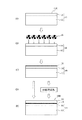
本発明の第1実施形態による半導体エピタキシャルウェーハ100の製造方法を図1に示す。まず、半導体ウェーハ10の表面10Aにクラスターイオン16を照射して、半導体ウェーハ10の表面10Aに、このクラスターイオン16の構成元素である炭素およびドーパント元素が固溶した改質層18を形成する第1工程(図1(A),(B))を行う。次に、半導体ウェーハ10をSC−1洗浄やHF洗浄など周知の洗浄方法で洗浄した後、半導体ウェーハ10の改質層18上に、改質層18におけるドーパント元素のピーク濃度よりもドーパント元素濃度が低いエピタキシャル層20を形成する第2工程(図1(D))を行う。図1(D)は、この製造方法の結果得られた半導体エピタキシャルウェーハ100の模式断面図である。
次に、上記製造方法により得られる半導体エピタキシャルウェーハ100,200について説明する。第1実施形態による半導体エピタキシャルウェーハ100および第2実施形態による半導体エピタキシャルウェーハ200は、図1(D)および図2(E)に示すように、半導体ウェーハ10と、この半導体ウェーハ10の表面に形成され、半導体ウェーハ10中に炭素およびドーパント元素が固溶してなる改質層18と、この改質層18上のエピタキシャル層20と、を有する。そして、いずれにおいても改質層18における、炭素の濃度プロファイルの半値幅W1およびドーパント元素の濃度プロファイルの半値幅W2がともに100nm以下であり、かつエピタキシャル層20におけるドーパント元素の濃度が、改質層18におけるドーパント元素のピーク濃度よりも低いことを特徴とする。
本発明の実施形態による固体撮像素子の製造方法は、上記の製造方法で製造されたエピタキシャルウェーハまたは上記のエピタキシャルウェーハ、すなわち半導体エピタキシャルウェーハ100,200の表面に位置するエピタキシャル層20に、固体撮像素子を形成することを特徴とする。この製造方法により得られる固体撮像素子は、従来に比べ製造工程の各処理中で発生する重金属汚染の影響を低減でき、白傷欠陥の発生を十分に抑制することができる。
まず、クラスターイオン照射とモノマーイオン注入の相違を明らかにするため、以下の実験を行った。
CZ単結晶シリコンインゴットから得たn型シリコンウェーハ(直径:300mm、厚さ:725μm、ドーパント:リン、ドーパント濃度:5×10¹⁴atoms/cm3)を用意した。次に、クラスターイオン発生装置(日新イオン機器社製、型番:CLARIS)を用いて、トリメチルホスフィン(C3H9P)をイオン化して、炭素のドーズ量5.0×1014atoms/cm2、リンのドーズ量1.7×1014atoms/cm2、炭素1原子あたりの加速電圧12.8keV/atom、リンの1原子あたりの加速電圧32keV/atomの条件で、シリコンウェーハに照射した。
参考例1と同じシリコンウェーハに対して、トリメチルホスフィンに替えて、トリメチルボラン(C3H9B)を材料ガスとして、クラスターイオンを生成し、ボロンのドーズ量1.7×10¹⁴atoms/cm2、ボロン1原子あたりの加速電圧を14.5kev/atomとした以外は、参考例1と同じ条件で、シリコンウェーハに照射した。
参考例1と同じシリコンウェーハに対して、クラスターイオン照射に替えて、CO2を材料ガスとして、炭素のモノマーイオンを生成し、ドーズ量5.0×10¹⁴atoms/cm2、加速電圧80keV/atomの条件で、シリコンウェーハに注入した。その後、ホスフィン(PH3)を材料ガスとして、リンのモノマーイオンを生成し、ドーズ量1.7×1014atoms/cm2、加速電圧80keV/atomの条件で、シリコンウェーハに注入した。
参考例1と同じシリコンウェーハに対して、クラスターイオン照射に替えて、CO2を材料ガスとして、炭素のモノマーイオンを生成し、ドーズ量5.0×10¹⁴atoms/cm2、加速電圧80keV/atomの条件で、シリコンウェーハに注入した。その後、BF2を材料ガスとして、ボロンのモノマーイオンを生成し、ドーズ量1.7×1014atoms/cm2、加速電圧80keV/atomの条件で、シリコンウェーハに注入した。
上記参考例1〜4で作製したサンプルについて、二次イオン質量分析(SIMS)により測定を行い、図4(A),(B)および図5(A),(B)に示す炭素およびドーパント元素の濃度プロファイルを得た。なお、横軸の深さはシリコンウェーハの表面をゼロとしている。図4(A),(B)および図5(A),(B)から明らかなように、クラスターイオン照射をした参考例1,2では、炭素濃度プロファイルおよびドーパント元素(リン、ボロン)濃度プロファイルがいずれもシャープであるが、モノマーイオン注入をした参考例3,4では、炭素濃度プロファイルおよびドーパント元素濃度プロファイルがブロードである。また、参考例3,4に比べて参考例1,2では、炭素およびドーパント元素の濃度プロファイルのピーク濃度はいずれも高く、ピーク位置もより半導体ウェーハ表面近傍に位置している。このことから、エピタキシャル層形成後も、各元素の濃度プロファイルの傾向は同様となることが推定される。
(実施例1)
CZ単結晶シリコンインゴットから得たn型シリコンウェーハ(厚さ:725μm、ドーパント種類:リン、ドーパント濃度:1×10¹⁵atoms/cm3)を用意した。次に、クラスターイオン発生装置(日新イオン機器社製、型番:CLARIS)を用いて、トリメチルホスフィン(C3H9P)のクラスターイオンを生成し、炭素のドーズ量5.0×1014atom/cm2、リンのドーズ量1.7×1014atom/cm2、炭素1原子あたり12.8keV/atom、ボロン1原子あたり12.8keV/atomの照射条件でシリコンウェーハに照射した。その後、シリコンウェーハをHF洗浄処理した後、枚葉式エピタキシャル成長装置(アプライドマテリアルズ社製)内に搬送し、装置内で1120℃の温度で30秒の水素ベーク処理を施した後、水素をキャリアガス、トリクロロシランをソースガス、ホスフィン(PH3)をドーパントガスとして1000〜1150℃でCVD法により、シリコンウェーハ上にシリコンのエピタキシャル層(厚さ:6μm、ドーパント種類:リン、ドーパント濃度:5×1015atoms/cm3)をエピタキシャル成長させ、本発明に従うシリコンエピタキシャルウェーハを作製した。
実施例1と同じシリコンウェーハに対して、トリメチルホスフィンに替えて、トリメチルボラン(C3H9B)を材料ガスとして、クラスターイオンを生成し、ボロンのドーズ量1.7×10¹⁴atoms/cm2、ボロン1原子あたりの加速電圧を14.5kev/atomとし、さらにエピタキシャル層(ドーパント種類:ボロン、ドーパント濃度:5×1015atoms/cm3)とした以外は、実施例1と同じ条件で、本発明に従うシリコンエピタキシャルウェーハを作製した。
実施例1と同じシリコンウェーハに対して、クラスターイオン照射に替えて、CO2を材料ガスとして、炭素のモノマーイオンを生成し、ドーズ量5.0×10¹⁴atoms/cm2、加速電圧80keV/atomの条件で、シリコンウェーハに注入した。その後、ホスフィン(PH3)を材料ガスとして、リンのモノマーイオンを生成し、ドーズ量1.7×1014atoms/cm2、加速電圧80keV/atomの条件でシリコンウェーハに注入した以外は、実施例1と同じ条件で、比較例にかかるシリコンエピタキシャルウェーハを作製した。
実施例1と同じシリコンウェーハに対して、クラスターイオン照射に替えて、CO2を材料ガスとして、炭素のモノマーイオンを生成し、ドーズ量5.0×10¹⁴atoms/cm2、加速電圧80keV/atomの条件で、シリコンウェーハに注入した。その後、BF2を材料ガスとして、ボロンのモノマーイオンを生成し、ドーズ量1.7×1014atoms/cm2、加速電圧80keV/atomの条件でシリコンウェーハに注入した以外は、実施例1と同じ条件で、比較例にかかるシリコンエピタキシャルウェーハを作製した。
実施例1と同じシリコンウェーハに対して、クラスターイオン照射に替えて、CO2を材料ガスとして、炭素のモノマーイオンを生成し、ドーズ量5.0×10¹⁴atoms/cm2、加速電圧80keV/atomの条件で、シリコンウェーハに注入した以外は、実施例1と同じ条件で、比較例にかかるシリコンエピタキシャルウェーハを作製した。
(1)SIMS測定
作製した各サンプルについてSIMS測定を行い、図6(A),(B)および図7(A),(B),(C)に示す炭素およびドーパント元素の濃度プロファイルを得た。ただし、図7(C)についてはドーパント元素を注入していないので、炭素の濃度プロファイルのみである。なお、横軸の深さはエピタキシャル層の表面をゼロとしている。また、作製した各サンプルについて、エピタキシャル層を1μmまで薄膜化した後にSIMS測定を行った。このとき得られた炭素およびドーパント元素の濃度プロファイルの半値幅、ピーク濃度、およびピーク位置(エピタキシャル層を除いたシリコンウェーハ表面からのピーク深さ)を、それぞれ以下の評価基準で分類して表1に示す。
半値幅
◎:100nm以下
○:100nm超〜125nm以下
△:125nm超
ピーク位置
◎:125nm以下
○:125nm超〜150nm以下
△:150nm超
ピーク濃度
◎:5.0×10¹⁹atoms/cm3以上
○:2.0×10¹⁹atoms/cm3以上〜5.0×1019atoms/cm3未満
△:2.0×10¹⁹atoms/cm3未満
作製した各サンプルのエピタキシャル層表面を、Ni汚染液(1.0×10¹⁴/cm2)およびCu汚染液(1.0×1014/cm2)でスピンコート汚染法を用いて故意に汚染し、引き続き1000℃、1時間の拡散熱処理を施した。その後、SIMS測定を行うことでゲッタリング性能を評価した。NiおよびCuの捕獲量(SIMSプロファイルの積分値)を以下のようにそれぞれ分類して、評価基準とした。評価結果を表1に示す。
◎:7.5×10¹³atoms/cm2以上〜1×1014atoms/cm2未満
○:5.0×10¹³atoms/cm2以上〜7.5×1013atoms/cm2未満
△:5.0×10¹³atoms/cm2未満

図6(A),(B)と、図7(A),(B),(C)とを比較すると、クラスターイオン照射により、実施例1,2では炭素およびドーパント元素が局所的かつ高濃度に固溶した改質層が形成されることが分かる。そして、表1に示すように、実施例1,2は、炭素およびドーパント元素の濃度プロファイルの半値幅がいずれも100nm以下であるために、NiおよびCuの両方に対して、比較例1〜3よりも優れたゲッタリング能力を発揮していることが分かる。
10A 半導体ウェーハの表面
12 バルク半導体ウェーハ
14 第1エピタキシャル層
16 クラスターイオン
18 改質層
20 (第2)エピタキシャル層
100 半導体エピタキシャルウェーハ
200 半導体エピタキシャルウェーハ
Claims (14)
- 半導体ウェーハの表面にクラスターイオンを照射して、該半導体ウェーハ表面に、前記クラスターイオンの構成元素である炭素およびドーパント元素が固溶した改質層を形成する第1工程と、
前記半導体ウェーハの改質層上に、該改質層における前記ドーパント元素のピーク濃度よりもドーパント元素の濃度が低いエピタキシャル層を形成する第2工程と、
を有し、該第2工程後の改質層における前記構成元素の深さ方向の濃度プロファイルの半値幅が100nm以下である半導体エピタキシャルウェーハを得ることを特徴とする半導体エピタキシャルウェーハの製造方法。 - 前記クラスターイオンが、前記炭素および前記ドーパント元素の両方を含む化合物をイオン化してなる請求項1に記載の半導体エピタキシャルウェーハの製造方法。
- 前記ドーパント元素が、ボロン、リン、砒素およびアンチモンからなる群より選択された1または2以上の元素である請求項1または2に記載の半導体エピタキシャルウェーハの製造方法。
- 前記半導体ウェーハが、シリコンウェーハである請求項1〜3いずれか1項に記載の半導体エピタキシャルウェーハの製造方法。
- 前記半導体ウェーハが、シリコンウェーハの表面にシリコンエピタキシャル層が形成されたエピタキシャルシリコンウェーハであり、前記第1工程において前記改質層は前記シリコンエピタキシャル層の表面に形成される請求項1〜3のいずれか1項に記載の半導体エピタキシャルウェーハの製造方法。
- 前記第1工程の後、前記第2工程の前に前記半導体ウェーハに対して結晶性回復のための熱処理を行う工程をさらに有する請求項1〜5のいずれか1項に記載の半導体エピタキシャルウェーハの製造方法。
- 半導体ウェーハと、該半導体ウェーハの表面に形成された、該半導体ウェーハ中に炭素およびドーパント元素が固溶してなる改質層と、該改質層上のエピタキシャル層と、を有し、
前記改質層における、前記炭素の濃度プロファイルの半値幅および前記ドーパント元素の濃度プロファイルの半値幅がともに100nm以下であり、
前記エピタキシャル層におけるドーパント元素の濃度が、前記改質層における前記ドーパント元素のピーク濃度よりも低いことを特徴とする半導体エピタキシャルウェーハ。 - 前記ドーパント元素が、ボロン、リン、砒素およびアンチモンからなる群より選択された1または2以上の元素である請求項7に記載の半導体エピタキシャルウェーハ。
- 前記半導体ウェーハが、シリコンウェーハである請求項7または8に記載の半導体エピタキシャルウェーハ。
- 前記半導体ウェーハが、シリコンウェーハの表面にシリコンエピタキシャル層が形成されたエピタキシャルシリコンウェーハであり、前記改質層は前記シリコンエピタキシャル層の表面に位置する請求項7または8に記載の半導体エピタキシャルウェーハ。
- 前記半導体ウェーハの表面からの深さが150nm以下の範囲内に、前記改質層における前記炭素および前記ドーパント元素の濃度プロファイルのピークが位置する請求項7〜10のいずれか1項に記載の半導体エピタキシャルウェーハ。
- 前記改質層における前記炭素の濃度プロファイルのピーク濃度が、1×10¹⁵atoms/cm3以上である請求項7〜11のいずれか1項に記載の半導体エピタキシャルウェーハ。
- 前記改質層における前記ドーパント元素の濃度プロファイルのピーク濃度が、1×10¹⁵atoms/cm3以上である請求項7〜12のいずれか1項に記載の半導体エピタキシャルウェーハ。
- 請求項1〜6のいずれか1項に記載の製造方法で製造されたエピタキシャルウェーハまたは請求項7〜13のいずれか1項に記載のエピタキシャルウェーハの、表面に位置するエピタキシャル層に、固体撮像素子を形成することを特徴とする固体撮像素子の製造方法。
Priority Applications (8)
| Application Number | Priority Date | Filing Date | Title |
|---|---|---|---|
| JP2012249731A JP5799936B2 (ja) | 2012-11-13 | 2012-11-13 | 半導体エピタキシャルウェーハの製造方法、半導体エピタキシャルウェーハ、および固体撮像素子の製造方法 |
| CN201380059278.XA CN104781919B (zh) | 2012-11-13 | 2013-11-11 | 半导体外延晶片的制造方法、半导体外延晶片以及固体摄像元件的制造方法 |
| KR1020157013183A KR101669603B1 (ko) | 2012-11-13 | 2013-11-11 | 반도체 에피텍셜 웨이퍼의 제조 방법, 반도체 에피텍셜 웨이퍼, 및 고체 촬상 소자의 제조 방법 |
| DE112013005401.9T DE112013005401T5 (de) | 2012-11-13 | 2013-11-11 | Verfahren zur Herstellung von Halbleiter-Epitaxiewafern, Halbleiter-Epitaxiewafer, und Verfahren zur Herstellung von Festkörper-Bildsensorvorrichtungen |
| PCT/JP2013/006610 WO2014076921A1 (ja) | 2012-11-13 | 2013-11-11 | 半導体エピタキシャルウェーハの製造方法、半導体エピタキシャルウェーハ、および固体撮像素子の製造方法 |
| US14/442,355 US20160181311A1 (en) | 2012-11-13 | 2013-11-11 | Method of producing semiconductor epitaxial wafer, semiconductor epitaxial wafer, and method of producing solid-state image sensing device |
| TW102141071A TWI514558B (zh) | 2012-11-13 | 2013-11-12 | 半導體磊晶晶圓的製造方法、半導體磊晶晶圓及固體攝影元件的製造方法 |
| US16/717,722 US20200127043A1 (en) | 2012-11-13 | 2019-12-17 | Method of producing semiconductor epitaxial wafer, semiconductor epitaxial wafer, and method of producing solid-state image sensing device |
Applications Claiming Priority (1)
| Application Number | Priority Date | Filing Date | Title |
|---|---|---|---|
| JP2012249731A JP5799936B2 (ja) | 2012-11-13 | 2012-11-13 | 半導体エピタキシャルウェーハの製造方法、半導体エピタキシャルウェーハ、および固体撮像素子の製造方法 |
Publications (3)
| Publication Number | Publication Date |
|---|---|
| JP2014099482A JP2014099482A (ja) | 2014-05-29 |
| JP2014099482A5 JP2014099482A5 (ja) | 2015-03-05 |
| JP5799936B2 true JP5799936B2 (ja) | 2015-10-28 |
Family
ID=50730855
Family Applications (1)
| Application Number | Title | Priority Date | Filing Date |
|---|---|---|---|
| JP2012249731A Active JP5799936B2 (ja) | 2012-11-13 | 2012-11-13 | 半導体エピタキシャルウェーハの製造方法、半導体エピタキシャルウェーハ、および固体撮像素子の製造方法 |
Country Status (7)
| Country | Link |
|---|---|
| US (2) | US20160181311A1 (ja) |
| JP (1) | JP5799936B2 (ja) |
| KR (1) | KR101669603B1 (ja) |
| CN (1) | CN104781919B (ja) |
| DE (1) | DE112013005401T5 (ja) |
| TW (1) | TWI514558B (ja) |
| WO (1) | WO2014076921A1 (ja) |
Families Citing this family (17)
| Publication number | Priority date | Publication date | Assignee | Title |
|---|---|---|---|---|
| JP6119637B2 (ja) * | 2014-02-26 | 2017-04-26 | 信越半導体株式会社 | アニール基板の製造方法、及び半導体装置の製造方法 |
| JP6539959B2 (ja) * | 2014-08-28 | 2019-07-10 | 株式会社Sumco | エピタキシャルシリコンウェーハおよびその製造方法、ならびに、固体撮像素子の製造方法 |
| JP6137165B2 (ja) * | 2014-12-25 | 2017-05-31 | 株式会社Sumco | 半導体エピタキシャルウェーハの製造方法および固体撮像素子の製造方法 |
| JP6354993B2 (ja) * | 2015-04-03 | 2018-07-11 | 信越半導体株式会社 | シリコンウェーハ及びシリコンウェーハの製造方法 |
| US10026843B2 (en) * | 2015-11-30 | 2018-07-17 | Taiwan Semiconductor Manufacturing Co., Ltd. | Fin structure of semiconductor device, manufacturing method thereof, and manufacturing method of active region of semiconductor device |
| JP6459948B2 (ja) * | 2015-12-15 | 2019-01-30 | 株式会社Sumco | 半導体エピタキシャルウェーハの製造方法および固体撮像素子の製造方法 |
| JP6759626B2 (ja) * | 2016-02-25 | 2020-09-23 | 株式会社Sumco | エピタキシャルウェーハの製造方法およびエピタキシャルウェーハ |
| JP2017201647A (ja) | 2016-05-02 | 2017-11-09 | ルネサスエレクトロニクス株式会社 | 半導体装置の製造方法 |
| JP6737066B2 (ja) * | 2016-08-22 | 2020-08-05 | 株式会社Sumco | エピタキシャルシリコンウェーハの製造方法、エピタキシャルシリコンウェーハ、及び固体撮像素子の製造方法 |
| JP6327393B1 (ja) * | 2017-02-28 | 2018-05-23 | 株式会社Sumco | エピタキシャルシリコンウェーハの不純物ゲッタリング能力の評価方法及びエピタキシャルシリコンウェーハ |
| JP6787268B2 (ja) * | 2017-07-20 | 2020-11-18 | 株式会社Sumco | 半導体エピタキシャルウェーハおよびその製造方法、ならびに固体撮像素子の製造方法 |
| JP2019080008A (ja) * | 2017-10-26 | 2019-05-23 | 信越半導体株式会社 | 基板の熱処理方法 |
| JP6801682B2 (ja) | 2018-02-27 | 2020-12-16 | 株式会社Sumco | 半導体エピタキシャルウェーハの製造方法及び半導体デバイスの製造方法 |
| JP6930459B2 (ja) * | 2018-03-01 | 2021-09-01 | 株式会社Sumco | 半導体エピタキシャルウェーハの製造方法 |
| KR102261633B1 (ko) * | 2019-02-01 | 2021-06-04 | 에스케이실트론 주식회사 | 에피택셜웨이퍼의 금속오염분석방법 |
| JP6988843B2 (ja) * | 2019-02-22 | 2022-01-05 | 株式会社Sumco | 半導体エピタキシャルウェーハ及びその製造方法 |
| JP7259791B2 (ja) * | 2020-03-25 | 2023-04-18 | 株式会社Sumco | シリコンウェーハへのクラスターイオン注入による白傷欠陥低減効果の評価方法及びエピタキシャルシリコンウェーハの製造方法 |
Family Cites Families (14)
| Publication number | Priority date | Publication date | Assignee | Title |
|---|---|---|---|---|
| JP3384506B2 (ja) * | 1993-03-30 | 2003-03-10 | ソニー株式会社 | 半導体基板の製造方法 |
| JP4016371B2 (ja) * | 1999-11-10 | 2007-12-05 | 信越半導体株式会社 | シリコンエピタキシャルウェーハの製造方法 |
| JP2006193800A (ja) | 2005-01-14 | 2006-07-27 | Canon Inc | 硬質炭素膜の成膜方法及び成膜装置 |
| KR100654354B1 (ko) | 2005-07-25 | 2006-12-08 | 삼성전자주식회사 | 게더링 기능을 가지는 저결함 에피택셜 반도체 기판, 이를이용한 이미지 센서 및 이의 제조 방법 |
| KR101455404B1 (ko) * | 2005-12-09 | 2014-10-27 | 세미이큅, 인코포레이티드 | 탄소 클러스터의 주입에 의한 반도체 디바이스의 제조를위한 시스템 및 방법 |
| US8110820B2 (en) * | 2006-06-13 | 2012-02-07 | Semequip, Inc. | Ion beam apparatus and method for ion implantation |
| JP2008311418A (ja) * | 2007-06-14 | 2008-12-25 | Shin Etsu Handotai Co Ltd | エピタキシャルウェーハおよびエピタキシャルウェーハの製造方法 |
| JP2010040864A (ja) * | 2008-08-06 | 2010-02-18 | Sumco Corp | エピタキシャルシリコンウェーハ及びその製造方法 |
| JP5099023B2 (ja) | 2009-01-27 | 2012-12-12 | 信越半導体株式会社 | エピタキシャルウエーハの製造方法及び固体撮像素子の製造方法 |
| JP2011151318A (ja) * | 2010-01-25 | 2011-08-04 | Renesas Electronics Corp | 半導体装置およびその製造方法 |
| JP2011253983A (ja) * | 2010-06-03 | 2011-12-15 | Disco Abrasive Syst Ltd | シリコンウェーハへのゲッタリング層付与方法 |
| FR2961013B1 (fr) * | 2010-06-03 | 2013-05-17 | Commissariat Energie Atomique | Procede pour eliminer des impuretes residuelles extrinseques dans un substrat en zno ou en znmgo de type n, et pour realiser un dopage de type p de ce substrat. |
| JP2012059849A (ja) * | 2010-09-08 | 2012-03-22 | Shin Etsu Handotai Co Ltd | シリコンエピタキシャルウェーハおよびシリコンエピタキシャルウェーハの製造方法 |
| US9263271B2 (en) * | 2012-10-25 | 2016-02-16 | Infineon Technologies Ag | Method for processing a semiconductor carrier, a semiconductor chip arrangement and a method for manufacturing a semiconductor device |
-
2012
- 2012-11-13 JP JP2012249731A patent/JP5799936B2/ja active Active
-
2013
- 2013-11-11 DE DE112013005401.9T patent/DE112013005401T5/de active Pending
- 2013-11-11 CN CN201380059278.XA patent/CN104781919B/zh active Active
- 2013-11-11 WO PCT/JP2013/006610 patent/WO2014076921A1/ja active Application Filing
- 2013-11-11 KR KR1020157013183A patent/KR101669603B1/ko active IP Right Grant
- 2013-11-11 US US14/442,355 patent/US20160181311A1/en not_active Abandoned
- 2013-11-12 TW TW102141071A patent/TWI514558B/zh active
-
2019
- 2019-12-17 US US16/717,722 patent/US20200127043A1/en active Pending
Also Published As
| Publication number | Publication date |
|---|---|
| TWI514558B (zh) | 2015-12-21 |
| WO2014076921A1 (ja) | 2014-05-22 |
| TW201423969A (zh) | 2014-06-16 |
| US20200127043A1 (en) | 2020-04-23 |
| CN104781919A (zh) | 2015-07-15 |
| CN104781919B (zh) | 2018-03-27 |
| JP2014099482A (ja) | 2014-05-29 |
| KR101669603B1 (ko) | 2016-10-26 |
| US20160181311A1 (en) | 2016-06-23 |
| KR20150066597A (ko) | 2015-06-16 |
| DE112013005401T5 (de) | 2015-07-30 |
Similar Documents
| Publication | Publication Date | Title |
|---|---|---|
| JP5799936B2 (ja) | 半導体エピタキシャルウェーハの製造方法、半導体エピタキシャルウェーハ、および固体撮像素子の製造方法 | |
| JP5673811B2 (ja) | 半導体エピタキシャルウェーハの製造方法、半導体エピタキシャルウェーハ、および固体撮像素子の製造方法 | |
| JP6065848B2 (ja) | 半導体エピタキシャルウェーハの製造方法、半導体エピタキシャルウェーハ、および固体撮像素子の製造方法 | |
| JP6278591B2 (ja) | 半導体エピタキシャルウェーハの製造方法、半導体エピタキシャルウェーハ、および固体撮像素子の製造方法 | |
| JP5799935B2 (ja) | 半導体エピタキシャルウェーハの製造方法、半導体エピタキシャルウェーハ、および固体撮像素子の製造方法 | |
| JP6107068B2 (ja) | エピタキシャルシリコンウェーハの製造方法、エピタキシャルシリコンウェーハ、および固体撮像素子の製造方法 | |
| JP6535432B2 (ja) | 半導体エピタキシャルウェーハの製造方法、半導体エピタキシャルウェーハ、および固体撮像素子の製造方法 | |
| JP6280301B2 (ja) | エピタキシャルシリコンウェーハの製造方法、エピタキシャルシリコンウェーハ、および固体撮像素子の製造方法 | |
| JP2017112276A (ja) | 半導体エピタキシャルウェーハの製造方法および固体撮像素子の製造方法 | |
| JP6289805B2 (ja) | 半導体エピタキシャルウェーハの製造方法、半導体エピタキシャルウェーハ、および固体撮像素子の製造方法 | |
| JP2017175145A (ja) | 半導体エピタキシャルウェーハの製造方法、半導体エピタキシャルウェーハ、および固体撮像素子の製造方法 | |
| JP6361779B2 (ja) | エピタキシャルシリコンウェーハの製造方法、エピタキシャルシリコンウェーハ、および固体撮像素子の製造方法 | |
| JP6278592B2 (ja) | 半導体エピタキシャルウェーハの製造方法、半導体エピタキシャルウェーハ、および固体撮像素子の製造方法 | |
| JP6318728B2 (ja) | 半導体エピタキシャルウェーハの製造方法、半導体エピタキシャルウェーハ、および固体撮像素子の製造方法 | |
| JP2015220242A (ja) | 半導体エピタキシャルウェーハの製造方法および固体撮像素子の製造方法 | |
| JP2017175143A (ja) | 半導体エピタキシャルウェーハの製造方法、半導体エピタキシャルウェーハ、および固体撮像素子の製造方法 | |
| JP2017183736A (ja) | 半導体エピタキシャルウェーハの製造方法、半導体エピタキシャルウェーハ、および固体撮像素子の製造方法 |
Legal Events
| Date | Code | Title | Description |
|---|---|---|---|
| A521 | Request for written amendment filed |
Free format text: JAPANESE INTERMEDIATE CODE: A523 Effective date: 20150114 |
|
| A621 | Written request for application examination |
Free format text: JAPANESE INTERMEDIATE CODE: A621 Effective date: 20150114 |
|
| A871 | Explanation of circumstances concerning accelerated examination |
Free format text: JAPANESE INTERMEDIATE CODE: A871 Effective date: 20150114 |
|
| A975 | Report on accelerated examination |
Free format text: JAPANESE INTERMEDIATE CODE: A971005 Effective date: 20150203 |
|
| A131 | Notification of reasons for refusal |
Free format text: JAPANESE INTERMEDIATE CODE: A131 Effective date: 20150210 |
|
| TRDD | Decision of grant or rejection written | ||
| A01 | Written decision to grant a patent or to grant a registration (utility model) |
Free format text: JAPANESE INTERMEDIATE CODE: A01 Effective date: 20150728 |
|
| A61 | First payment of annual fees (during grant procedure) |
Free format text: JAPANESE INTERMEDIATE CODE: A61 Effective date: 20150810 |
|
| R150 | Certificate of patent or registration of utility model |
Ref document number: 5799936 Country of ref document: JP Free format text: JAPANESE INTERMEDIATE CODE: R150 |
|
| R250 | Receipt of annual fees |
Free format text: JAPANESE INTERMEDIATE CODE: R250 |
|
| R250 | Receipt of annual fees |
Free format text: JAPANESE INTERMEDIATE CODE: R250 |
|
| R250 | Receipt of annual fees |
Free format text: JAPANESE INTERMEDIATE CODE: R250 |
|
| R250 | Receipt of annual fees |
Free format text: JAPANESE INTERMEDIATE CODE: R250 |
|
| R250 | Receipt of annual fees |
Free format text: JAPANESE INTERMEDIATE CODE: R250 |
|
| R250 | Receipt of annual fees |
Free format text: JAPANESE INTERMEDIATE CODE: R250 |