WO2015097903A1 - 電子写真用感光体、その製造方法および電子写真装置 - Google Patents
電子写真用感光体、その製造方法および電子写真装置 Download PDFInfo
- Publication number
- WO2015097903A1 WO2015097903A1 PCT/JP2013/085250 JP2013085250W WO2015097903A1 WO 2015097903 A1 WO2015097903 A1 WO 2015097903A1 JP 2013085250 W JP2013085250 W JP 2013085250W WO 2015097903 A1 WO2015097903 A1 WO 2015097903A1
- Authority
- WO
- WIPO (PCT)
- Prior art keywords
- resin
- layer
- electrophotographic photoreceptor
- charge transport
- iii
- Prior art date
- Legal status (The legal status is an assumption and is not a legal conclusion. Google has not performed a legal analysis and makes no representation as to the accuracy of the status listed.)
- Ceased
Links
Images

Classifications
-
- G—PHYSICS
- G03—PHOTOGRAPHY; CINEMATOGRAPHY; ANALOGOUS TECHNIQUES USING WAVES OTHER THAN OPTICAL WAVES; ELECTROGRAPHY; HOLOGRAPHY
- G03G—ELECTROGRAPHY; ELECTROPHOTOGRAPHY; MAGNETOGRAPHY
- G03G5/00—Recording-members for original recording by exposure, e.g. to light, to heat or to electrons; Manufacture thereof; Selection of materials therefor
- G03G5/02—Charge-receiving layers
- G03G5/04—Photoconductive layers; Charge-generation layers or charge-transporting layers; Additives therefor; Binders therefor
- G03G5/05—Organic bonding materials; Methods for coating a substrate with a photoconductive layer; Inert supplements for use in photoconductive layers
- G03G5/0528—Macromolecular bonding materials
- G03G5/0557—Macromolecular bonding materials obtained otherwise than by reactions only involving carbon-to-carbon unsatured bonds
- G03G5/0567—Other polycondensates comprising oxygen atoms in the main chain; Phenol resins
-
- G—PHYSICS
- G03—PHOTOGRAPHY; CINEMATOGRAPHY; ANALOGOUS TECHNIQUES USING WAVES OTHER THAN OPTICAL WAVES; ELECTROGRAPHY; HOLOGRAPHY
- G03G—ELECTROGRAPHY; ELECTROPHOTOGRAPHY; MAGNETOGRAPHY
- G03G5/00—Recording-members for original recording by exposure, e.g. to light, to heat or to electrons; Manufacture thereof; Selection of materials therefor
- G03G5/02—Charge-receiving layers
- G03G5/04—Photoconductive layers; Charge-generation layers or charge-transporting layers; Additives therefor; Binders therefor
- G03G5/043—Photoconductive layers characterised by having two or more layers or characterised by their composite structure
- G03G5/047—Photoconductive layers characterised by having two or more layers or characterised by their composite structure characterised by the charge-generation layers or charge transport layers
-
- G—PHYSICS
- G03—PHOTOGRAPHY; CINEMATOGRAPHY; ANALOGOUS TECHNIQUES USING WAVES OTHER THAN OPTICAL WAVES; ELECTROGRAPHY; HOLOGRAPHY
- G03G—ELECTROGRAPHY; ELECTROPHOTOGRAPHY; MAGNETOGRAPHY
- G03G5/00—Recording-members for original recording by exposure, e.g. to light, to heat or to electrons; Manufacture thereof; Selection of materials therefor
- G03G5/02—Charge-receiving layers
- G03G5/04—Photoconductive layers; Charge-generation layers or charge-transporting layers; Additives therefor; Binders therefor
- G03G5/05—Organic bonding materials; Methods for coating a substrate with a photoconductive layer; Inert supplements for use in photoconductive layers
- G03G5/0525—Coating methods
-
- G—PHYSICS
- G03—PHOTOGRAPHY; CINEMATOGRAPHY; ANALOGOUS TECHNIQUES USING WAVES OTHER THAN OPTICAL WAVES; ELECTROGRAPHY; HOLOGRAPHY
- G03G—ELECTROGRAPHY; ELECTROPHOTOGRAPHY; MAGNETOGRAPHY
- G03G5/00—Recording-members for original recording by exposure, e.g. to light, to heat or to electrons; Manufacture thereof; Selection of materials therefor
- G03G5/02—Charge-receiving layers
- G03G5/04—Photoconductive layers; Charge-generation layers or charge-transporting layers; Additives therefor; Binders therefor
- G03G5/05—Organic bonding materials; Methods for coating a substrate with a photoconductive layer; Inert supplements for use in photoconductive layers
- G03G5/0528—Macromolecular bonding materials
- G03G5/0557—Macromolecular bonding materials obtained otherwise than by reactions only involving carbon-to-carbon unsatured bonds
- G03G5/056—Polyesters
-
- G—PHYSICS
- G03—PHOTOGRAPHY; CINEMATOGRAPHY; ANALOGOUS TECHNIQUES USING WAVES OTHER THAN OPTICAL WAVES; ELECTROGRAPHY; HOLOGRAPHY
- G03G—ELECTROGRAPHY; ELECTROPHOTOGRAPHY; MAGNETOGRAPHY
- G03G5/00—Recording-members for original recording by exposure, e.g. to light, to heat or to electrons; Manufacture thereof; Selection of materials therefor
- G03G5/02—Charge-receiving layers
- G03G5/04—Photoconductive layers; Charge-generation layers or charge-transporting layers; Additives therefor; Binders therefor
- G03G5/05—Organic bonding materials; Methods for coating a substrate with a photoconductive layer; Inert supplements for use in photoconductive layers
- G03G5/0528—Macromolecular bonding materials
- G03G5/0557—Macromolecular bonding materials obtained otherwise than by reactions only involving carbon-to-carbon unsatured bonds
- G03G5/0564—Polycarbonates
-
- G—PHYSICS
- G03—PHOTOGRAPHY; CINEMATOGRAPHY; ANALOGOUS TECHNIQUES USING WAVES OTHER THAN OPTICAL WAVES; ELECTROGRAPHY; HOLOGRAPHY
- G03G—ELECTROGRAPHY; ELECTROPHOTOGRAPHY; MAGNETOGRAPHY
- G03G5/00—Recording-members for original recording by exposure, e.g. to light, to heat or to electrons; Manufacture thereof; Selection of materials therefor
- G03G5/02—Charge-receiving layers
- G03G5/04—Photoconductive layers; Charge-generation layers or charge-transporting layers; Additives therefor; Binders therefor
- G03G5/05—Organic bonding materials; Methods for coating a substrate with a photoconductive layer; Inert supplements for use in photoconductive layers
- G03G5/0528—Macromolecular bonding materials
- G03G5/0596—Macromolecular compounds characterised by their physical properties
Definitions
- the present invention relates to an electrophotographic photoreceptor (hereinafter also referred to as “photoreceptor”), a manufacturing method thereof, and an electrophotographic apparatus. More specifically, the present invention relates to an electrophotographic photoreceptor, which is mainly composed of a conductive substrate and a photosensitive layer containing an organic material, and is used in an electrophotographic printer, a copying machine, a fax machine, etc., a manufacturing method thereof, and an electrophotographic apparatus. .
- the electrophotographic photoreceptor has a basic structure in which a photosensitive layer having a photoconductive function is provided on a conductive substrate.
- organic electrophotographic photoreceptors using organic compounds as functional components responsible for charge generation and transport have been actively researched and developed due to advantages such as material diversity, high productivity, and safety. Application to printers and printers is ongoing.
- a photoreceptor needs to have a function of holding a surface charge in a dark place, a function of receiving light to generate a charge, and a function of transporting the generated charge.
- So-called laminated type (functional separation type) photoreceptor comprising a photosensitive layer in which a functionally separated layer is laminated on a charge transporting layer, which has a function of retaining light and a function of transporting charges generated in the charge generation layer upon light reception There is.
- the photosensitive layer is generally formed by applying a coating solution prepared by dissolving or dispersing a charge generating material, a charge transporting material and a resin binder in an organic solvent onto a conductive substrate.
- a coating solution prepared by dissolving or dispersing a charge generating material, a charge transporting material and a resin binder in an organic solvent onto a conductive substrate.
- a polycarbonate which is resistant to friction generated between paper and a blade for toner removal, has excellent flexibility, and has good exposure transparency.
- Often used as a binder Among these, bisphenol Z-type polycarbonate is widely used as the resin binder.
- a technique using such a polycarbonate as a resin binder is described in Patent Document 1 and the like.
- Methods for charging the photoconductor include a non-contact charging method in which the charging member such as scorotron is not in contact with the photoconductor, and contact in which the charging member made of a semiconductive rubber roller or brush contacts the photoconductor.
- a charging method There is a charging method.
- the contact charging method has the advantage that less corona discharge occurs in the vicinity of the photoconductor than the non-contact charging method, and therefore less ozone is generated and the applied voltage may be low. Therefore, since a more compact, low-cost, and low environmental pollution electrophotographic apparatus can be realized, it is mainly used for medium-sized to small-sized apparatuses.
- scraping with a blade, a simultaneous development cleaning process, or the like is mainly used.
- the untransferred residual toner on the surface of the photoreceptor is scraped off by the blade and may be collected in a collection box for waste toner, or may be returned to the developing device again. Therefore, when using such a scraper cleaner with a blade, a toner collection box or a space for recycling is required, and it is necessary to monitor whether the collection box is full.
- paper dust or external additives stay on the blade, the surface of the photoconductor may be damaged and the life of the photoconductor may be shortened. Therefore, there is a case where a process for collecting the toner in the development process or for attracting the residual toner adhering to the surface of the photoreceptor magnetically or electrically just before the development process may be provided.
- Patent Documents 2 and 3 propose a method of adding a filler to the surface layer of the photoreceptor in order to improve the durability of the photoreceptor surface.
- the aggregate of the filler exists, the transparency of the layer is reduced, or the exposure light is scattered by the filler, so that charge transport and charge generation become non-uniform and image characteristics are deteriorated.
- a method of adding a dispersing agent in order to improve the dispersibility of the filler. In this case, since the dispersing agent itself affects the photoreceptor characteristics, it is possible to achieve both the dispersibility of the filler and the photoreceptor characteristics. It was difficult.
- Patent Document 4 proposes a method for improving wear resistance using a resin having a terminal structure having a siloxane structure introduced therein.
- Patent Document 5 it is proposed to use polyarylate as a resin binder for the photosensitive layer, and various studies have been made for the purpose of improving durability and mechanical strength.
- Patent Document 6 proposes a photoreceptor using a polyarylate resin having a siloxane structure obtained by using phenol-modified polysiloxane as a siloxane component and a polycarbonate resin for a photosensitive layer.
- Patent Document 7 proposes an electrophotographic apparatus including a photoconductor including a structural unit of polyarylate resin.
- Patent Documents 8 and 9 propose a photoreceptor using a polyarylate resin as a photosensitive layer.
- a method of forming a surface protective layer on the photosensitive layer has been proposed for the purpose of protecting the photosensitive layer, improving mechanical strength, and improving surface lubricity.
- the method of forming the surface protective layer has a problem that it is difficult to form a film on the charge transport layer, and it is difficult to sufficiently achieve both the charge transport performance and the charge retention function.
- JP-A-61-62040 JP-A-1-205171 Japanese Patent Laid-Open No. 7-333881 JP 2002-128883 A JP 2005-115091 A JP 2002-214807 A JP 2004-93865 A JP 2007-121751 A JP 2010-96929 A
- the technique disclosed in the above patent document cannot sufficiently secure the electrical characteristics and image characteristics while sufficiently reducing the amount of wear on the surface of the photoreceptor.
- an object of the present invention is to provide an electrophotographic photoreceptor, a method for producing the same, and an electrophotographic apparatus that can reduce the amount of wear on the surface and obtain a good image.
- the present inventors have included a resin having specific structural characteristics in a layer exposed on the surface of the photoconductor, thereby providing a highly durable photoconductor for electrophotography. As a result, the present invention has been completed.
- the electrophotographic photoreceptor of the present invention is an electrophotographic photoreceptor having a photosensitive layer on a conductive substrate, wherein the photosensitive layer has a helical structure with a molecular structure optimized using molecular dynamics calculation.
- the resin contains a resin, and the resin has a ratio r / l of a spiral structure diameter (r) to a spiral interval (l) in the range of 0.04 to 1.0. It is what.
- the optimization calculation of the molecular structure of the resin can be performed using a simulator such as J-OCTA (manufactured by JSOL).
- a molecular dynamics simulation program to be used atomic model conditions, the number of atoms and force field parameters are selected, temperature conditions, integration conditions and optimization calculation conditions are determined, and an optimized three-dimensional molecular structure is created.
- the diameter (r) and the helical interval (l) of the helical structure are obtained from the molecular coordinates, and the value of r / l is calculated.
- the present inventors have successfully used a resin having a molecular structure in which the value of r / l is in the range of 0.04 or more and 1.0 or less for the photosensitive layer exposed on the surface of the photoreceptor. It was found that printing durability can be obtained.
- a resin having a structure in which the value of r / l falls within the above range the effect of entanglement of the helical molecules constituting the resin can be obtained satisfactorily, and the strength of the layer is improved. Therefore, it is estimated that the wear resistance is improved.
- the helical structural unit of the molecules constituting the resin becomes large, the sufficient entanglement effect between the molecules cannot be obtained, and the wear improvement effect cannot be obtained.
- the value of r / l is larger than 1.0, the helix spacing of the molecules is narrow and sufficient entanglement between the molecules does not proceed, so that the effect of improving the wear cannot be obtained, and the molecular structure Therefore, the molecular weight sufficient to form the photosensitive layer cannot be obtained due to steric hindrance by the molecular chain itself in the state of the oligomer having a low polymerization degree when the resin is actually synthesized.
- a polycarbonate resin or a polyarylate resin having a helical structure in which the value of r / l falls within the above range an effect of improving wear can be obtained.
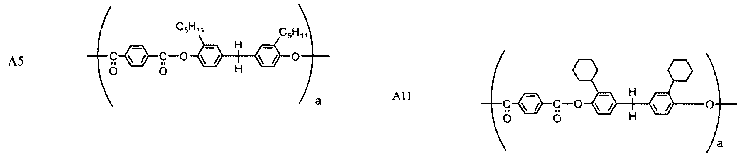
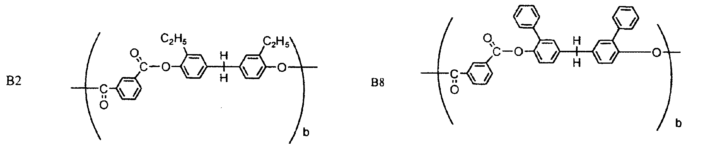
- the structural unit of the polyarylate resin having such characteristics include those represented by the following chemical structural formula 1.
- partial structural formulas (A), (B), (C) and (D) each represent a structural unit constituting the resin, and a, b, c and d represent each structural unit (A ), (B), (C) and (D), a + b + c + d is 100 mol%
- R 1 and R 2 may be the same or different, and an alkyl group having 1 to 8 carbon atoms, A cycloalkyl group which may have a substituent, or an aryl group which may have a substituent;
- R 3 and R 4 may be the same or different and are each a hydrogen atom, a carbon number of 1-8;
- An alkyl group, an optionally substituted cycloalkyl group, or an optionally substituted aryl group, or R 3 and R 4 are cyclic with the carbon atom to which they are attached.
- a structure may be formed. The other may be bonded to two of the arylene group.
- R 1 and R 2 are linear or monobranched alkyl groups having 1 to 8 carbon atoms, or aryl groups that may have a substituent.
- R 3 and R 4 are a hydrogen atom or a methyl group.
- the aryl group represented by R 1 and R 2 preferably has a paraphenylene structure having 1 to 5 repeats.
- a + b + c + d of the structural unit represented by the chemical structural formula 1 when the total amount a + b + c + d of the structural unit represented by the chemical structural formula 1 is 100 mol%, c and d are preferably 0 mol%. This is because if the structural units (C) and (D) are included, synthesis is considered difficult when the monomer molecular weight of the structural units (A) and (B) is large and the steric hindrance is large. . Furthermore, a + b is preferably 65 mol% or more and less than 100 mol%, and more preferably 70 mol% or more and less than 100 mol%.
- the mol% ratio of a and b is preferably 90:10 to 10:90. If a is less than 10 mol%, sufficient film hardness may not be obtained. On the other hand, when a exceeds 90 mol%, there is a possibility that sufficient compatibility with a solvent or a functional material cannot be obtained when a coating solution is used.
- the photosensitive layer may include at least a charge generation layer and a charge transport layer, and the charge transport layer may include the resin and a charge transport material.
- the generation layer and the charge transport layer can be laminated on the conductive substrate in this order.
- the photosensitive layer may include the resin, a charge generation material, and a charge transport material.
- the charge transport material includes a hole transport material and an electron transport material. It is preferable to contain.
- the photosensitive layer includes at least a charge transport layer and a charge generation layer, and the charge generation layer includes the resin, a charge generation material, and a charge transport material. In this case, the charge transport layer and the charge generation layer may be laminated on the conductive substrate in this order.
- the electrophotographic photoreceptor production method of the present invention is a method for producing an electrophotographic photoreceptor comprising a step of forming a photosensitive layer by applying a coating solution containing at least a resin binder on a conductive substrate.
- the resin binder contains a resin whose molecular structure optimized using molecular dynamics calculation is a helical structure, and the resin has a helical structure diameter (r) and a helical interval (l)
- the ratio r / l is in the range of 0.04 to 1.0.
- a resin having a repeating unit represented by the above chemical structural formula 1 can be suitably used as the resin.
- the electrophotographic apparatus of the present invention is characterized in that the electrophotographic photoreceptor is mounted.
- the resin having the above specific structure as the resin binder of the photosensitive layer, it is possible to reduce the amount of wear on the surface of the photosensitive member while maintaining the electrophotographic characteristics of the photosensitive member. It was revealed that the mechanical strength could also be improved. Although this mechanism is not clear, when such a resin is contained in the photosensitive layer, the molecules constituting the resin take a spiral structure in the layer, which increases the number of entanglements between the molecules in the layer. It is presumed that the durability against wear due to external force applied to the layer is improved.
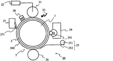
- FIG. 1 is a schematic configuration diagram illustrating an example of an electrophotographic apparatus according to the present invention. 1 is a 1 H-NMR spectrum of a copolymerized polyarylate resin (III-1).
- the electrophotographic photosensitive member is a so-called negatively charged laminated type photosensitive member and positively charged laminated type photosensitive member as a laminated type (functional separation type) photosensitive member, and a single layer type mainly used in a positively charged type.
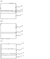
- FIG. 1 is a schematic cross-sectional view showing an example of the electrophotographic photoreceptor of the present invention, in which (a) is a negatively chargeable laminated electrophotographic photoreceptor, and (b) is a positively charged single layer type.
- An electrophotographic photoreceptor shows a positively charged laminated electrophotographic photoreceptor.
- an undercoat layer 2 a charge generation layer 4 having a charge generation function, and a charge transport layer 5 having a charge transport function are provided on a conductive substrate 1.
- the photosensitive layers are sequentially laminated.
- an undercoat layer 2 and a single layer type photosensitive layer 3 having both charge generation and charge transport functions are sequentially laminated on a conductive substrate 1. Yes.
- the undercoat layer 2, the charge transport layer 5 having a charge transport function, and the charge having both charge generation and charge transport functions are provided on the conductive substrate 1.
- a photosensitive layer having the generation layer 4 is sequentially laminated.
- the undercoat layer 2 may be provided as necessary.
- the “photosensitive layer” of the present invention includes both a laminated photosensitive layer in which a charge generation layer and a charge transport layer are laminated, and a single-layer photosensitive layer.
- the conductive substrate 1 serves as a support for each layer constituting the photoconductor as well as serving as an electrode of the photoconductor, and may have any shape such as a cylindrical shape, a plate shape, or a film shape.
- a metal such as aluminum, stainless steel, nickel, or the like such as glass, resin, etc., subjected to a conductive treatment can be used.
- the undercoat layer 2 is composed of a resin-based layer or a metal oxide film such as alumite.
- the undercoat layer 2 is used for purposes such as controlling charge injection from the conductive substrate 1 to the photosensitive layer, covering defects on the surface of the conductive substrate, and improving adhesion between the photosensitive layer and the conductive substrate 1. And provided as necessary.
- the resin material used for the undercoat layer 2 include insulating polymers such as casein, polyvinyl alcohol, polyamide, melamine, and cellulose, and conductive polymers such as polythiophene, polypyrrole, and polyaniline. Alternatively, they can be used in combination as appropriate. These resins may be used by containing a metal oxide such as titanium dioxide or zinc oxide.
- the charge generation layer 4 is formed by a method such as applying a coating liquid in which particles of a charge generation material are dispersed in a resin binder, and receives light to generate charges.
- the charge generation layer 4 has a high charge generation efficiency, and at the same time, it is important to inject the generated charges into the charge transport layer 5.
- charge generation materials include phthalocyanines such as X-type metal-free phthalocyanine, ⁇ -type metal-free phthalocyanine, ⁇ -type titanyl phthalocyanine, ⁇ -type titanyl phthalocyanine, Y-type titanyl phthalocyanine, ⁇ -type titanyl phthalocyanine, amorphous-type titanyl phthalocyanine, and ⁇ -type copper phthalocyanine.
- phthalocyanines such as X-type metal-free phthalocyanine, ⁇ -type metal-free phthalocyanine, ⁇ -type titanyl phthalocyanine, ⁇ -type titanyl phthalocyanine, Y-type titanyl phthalocyanine, ⁇ -type titanyl phthalocyanine, amorphous-type titanyl phthalocyanine, and ⁇ -type copper phthalocyanine.
- the content of the charge generation material in the charge generation layer 4 is preferably 20 to 80% by mass and more preferably 30 to 70% by mass with respect to the solid content in the charge generation layer 4.
- the charge generation layer 4 Since the charge generation layer 4 only needs to have a charge generation function, its film thickness is generally 1 ⁇ m or less, and preferably 0.5 ⁇ m or less.
- the charge generation layer 4 can also be used with a charge generation material as a main component and a charge transport material or the like added thereto.
- the resin binder of the charge generation layer 4 polycarbonate resin, polyester resin, polyamide resin, polyurethane resin, vinyl chloride resin, vinyl acetate resin, phenoxy resin, polyvinyl acetal resin, polyvinyl butyral resin, polystyrene resin, polysulfone resin, diallyl phthalate resin Further, it is possible to use a combination of a polymer and a copolymer of a methacrylic ester resin as appropriate.
- a resin having the above spiral structure can be arbitrarily used as the resin binder of the charge generation layer 4.
- the charge transport layer 5 is mainly composed of a charge transport material and a resin binder.
- a resin having the above spiral structure as a resin binder of the charge transport layer 5 disposed on the surface side of the photosensitive layer. Thereby, the desired effect of the present invention can be obtained.
- the resin having the spiral structure may be used alone or in combination with other resins.
- Such other resins include other polyarylate resins, bisphenol A type, bisphenol Z type, bisphenol A type-biphenyl copolymer, various other polycarbonate resins such as bisphenol Z type-biphenyl copolymer, polyphenylene resin, polyester Resin, polyvinyl acetal resin, polyvinyl butyral resin, polyvinyl alcohol resin, vinyl chloride resin, vinyl acetate resin, polyethylene resin, polypropylene resin, acrylic resin, polyurethane resin, epoxy resin, melamine resin, silicone resin, polyamide resin, polystyrene resin, polyacetal Resins, polysulfone resins, methacrylic ester polymers, copolymers thereof, and the like can be used.
- the same kind of resins having different molecular weights may be mixed and used.
- the content of the resin binder in the charge transport layer 5 is preferably 10 to 90% by mass, and more preferably 20 to 80% by mass with respect to the solid content of the charge transport layer 5. Furthermore, the content of the resin having the helical structure in the resin binder is preferably in the range of 1% by mass to 100% by mass, and more preferably in the range of 5% by mass to 80% by mass.
- the weight average molecular weight of the resin having the helical structure is preferably 5000 to 250,000, more preferably 10,000 to 200000 in GPC (gel permeation chromatography) analysis in terms of polystyrene.
- constituent monomers of these resins (I-1) to (I-22) for example, bisphenols as shown in the following M1 to M12 can be used, but are not limited thereto.
- charge transport material of the charge transport layer 5 various hydrazone compounds, styryl compounds, diamine compounds, butadiene compounds, indole compounds, and the like can be used alone or in combination as appropriate.
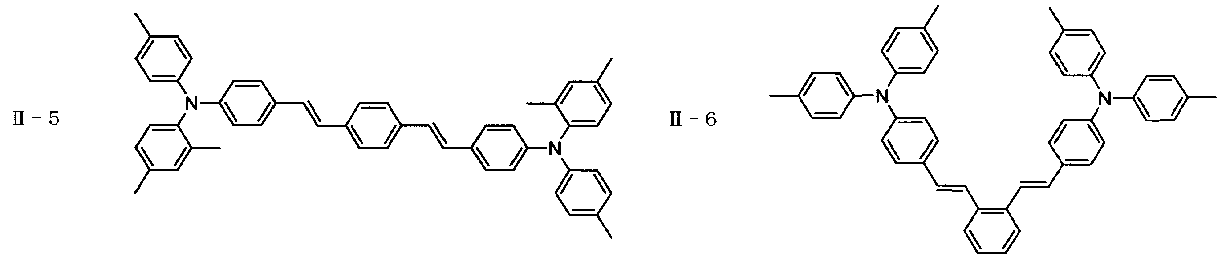
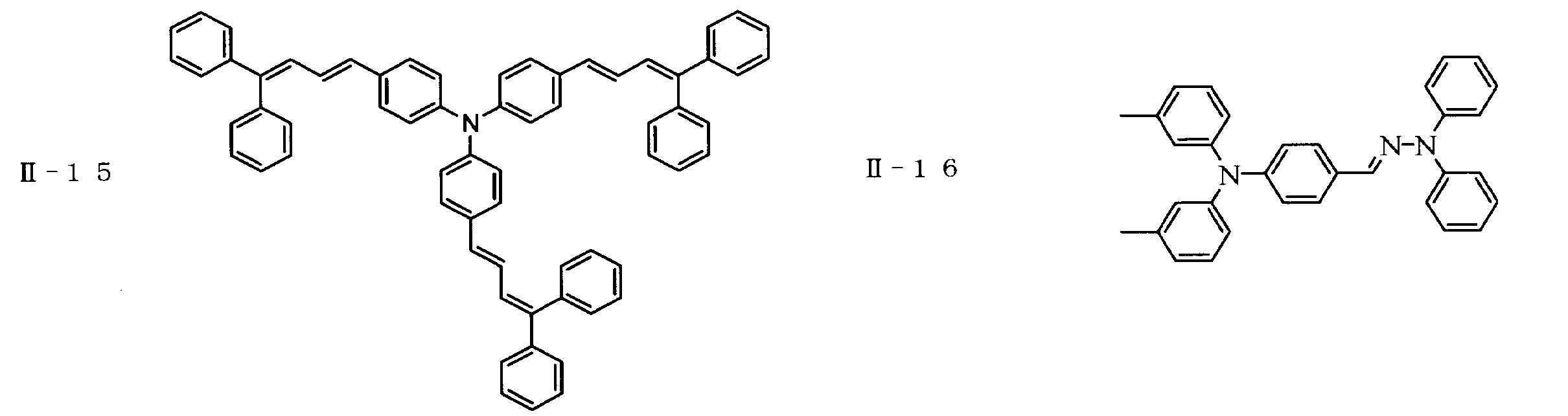
- Examples of such a charge transport material include, but are not limited to, those shown in the following (II-1) to (II-22).
- the film thickness of the charge transport layer 5 is preferably in the range of 3 to 50 ⁇ m and more preferably in the range of 15 to 40 ⁇ m in order to maintain a practically effective surface potential.
- the single layer type photosensitive layer 3 is mainly composed of a charge generation material, a hole transport material, an electron transport material (acceptor compound), and a resin binder.
- the present invention in the case of a positively charged single layer type photoreceptor, it is necessary to use a resin having the above spiral structure as the resin binder of the single layer type photosensitive layer 3. Thereby, the desired effect of the present invention can be obtained.
- the resin having such a helical structure include those described above.
- the resin having the spiral structure may be used alone or in combination with other resins.
- other resins include various other polycarbonate resins such as bisphenol A type, bisphenol Z type, bisphenol A type-biphenyl copolymer, bisphenol Z type-biphenyl copolymer, polyphenylene resin, polyester resin, polyvinyl acetal resin, Polyvinyl butyral resin, polyvinyl alcohol resin, vinyl chloride resin, vinyl acetate resin, polyethylene resin, polypropylene resin, acrylic resin, polyurethane resin, epoxy resin, melamine resin, silicone resin, polyamide resin, polystyrene resin, polyacetal resin, other polyarylate Resins, polysulfone resins, methacrylic ester polymers, copolymers thereof, and the like can be used. Furthermore, the same kind of resins having different molecular weights may be mixed and used.
- the content of the resin binder is preferably 10 to 90% by mass, and more preferably 20 to 80% by mass with respect to the solid content of the single-layer type photosensitive layer 3.
- the content of the resin having the helical structure in the resin binder is preferably in the range of 1% by mass to 100% by mass, and more preferably in the range of 5% by mass to 80% by mass.
- the charge generation material of the single-layer type photosensitive layer 3 for example, a phthalocyanine pigment, an azo pigment, an anthrone pigment, a perylene pigment, a perinone pigment, a polycyclic quinone pigment, a squarylium pigment, a thiapyrylium pigment, a quinacridone pigment, etc. Can do.
- a phthalocyanine pigment for example, a phthalocyanine pigment, an azo pigment, an anthrone pigment, a perylene pigment, a perinone pigment, a polycyclic quinone pigment, a squarylium pigment, a thiapyrylium pigment, a quinacridone pigment, etc.
- the azo pigment is a disazo pigment, a trisazo pigment
- the perylene pigment is N, N′-bis (3,5-dimethylphenyl) -3,4: 9,10-perylene.
- metal-free phthalocyanine As the bis (carboximide) and phthalocyanine pigments, it is preferable to use metal-free phthalocyanine, copper phthalocyanine, and titanyl phthalocyanine. Also, X-type metal-free phthalocyanine, ⁇ -type metal-free phthalocyanine, ⁇ -type copper phthalocyanine, ⁇ -type titanyl phthalocyanine, ⁇ -type titanyl phthalocyanine, Y-type titanyl phthalocyanine, amorphous-type titanyl phthalocyanine, Japanese Patent Application Laid-Open No. 8-209003, US Pat.
- the content of the charge generating material is preferably 0.1 to 20% by mass, and more preferably 0.5 to 10% by mass with respect to the solid content of the single-layer type photosensitive layer 3.
- Examples of the hole transport material of the single-layer type photosensitive layer 3 include hydrazone compounds, pyrazoline compounds, pyrazolone compounds, oxadiazole compounds, oxazole compounds, arylamine compounds, benzidine compounds, stilbene compounds, styryl compounds, poly-N— Vinyl carbazole, polysilane, etc. can be used. These hole transport materials can be used alone or in combination of two or more. As the hole transport material used in the present invention, a material that is excellent in the ability to transport holes generated during light irradiation and that is suitable in combination with a charge generation material is preferable.
- the content of the hole transport material is preferably 3 to 80% by mass, and more preferably 5 to 60% by mass with respect to the solid content of the single-layer type photosensitive layer 3.
- succinic anhydride succinic anhydride, maleic anhydride, dibromosuccinic anhydride, phthalic anhydride, 3-nitrophthalic anhydride, 4-nitrophthalic anhydride, anhydrous Pyromellitic acid, pyromellitic acid, trimellitic acid, trimellitic anhydride, phthalimide, 4-nitrophthalimide, tetracyanoethylene, tetracyanoquinodimethane, chloranil, bromanyl, o-nitrobenzoic acid, malononitrile, trinitrofluorenone, Trinitrothioxanthone, dinitrobenzene, dinitroanthracene, dinitroacridine, nitroanthraquinone, dinitroanthraquinone, thiopyran compounds, quinone compounds, benzoquinone compounds, diphenoquinone compounds, naphthoquinone compounds, anthraquinone compounds Compounds,
- the film thickness of the single-layer type photosensitive layer 3 is preferably in the range of 3 to 100 ⁇ m and more preferably in the range of 5 to 40 ⁇ m in order to maintain a practically effective surface potential.
- the charge transport layer 5 is mainly composed of a charge transport material and a resin binder.
- the charge transporting material and the resin binder the same materials as those mentioned for the charge transporting layer 5 of the negatively charged laminated photoreceptor can be used.
- the content of each material and the film thickness of the charge transport layer 5 can be the same as those of the negatively charged laminated photoreceptor.
- a resin having the above spiral structure can be arbitrarily used as the resin binder of the charge transport layer 5.
- the charge generation layer 4 provided on the charge transport layer 5 is mainly composed of a charge generation material, a hole transport material, an electron transport material (acceptor compound), and a resin binder.
- the charge generation material, the hole transport material, the electron transport material, and the resin binder the same materials as those mentioned for the single layer type photosensitive layer 3 of the single layer type photoreceptor can be used.
- the content of each material and the film thickness of the charge generation layer 4 can be the same as those of the single-layer photosensitive layer 3 of the single-layer photoreceptor.
- either a laminated type or a single layer type photosensitive layer contains an antioxidant, a light stabilizer and other anti-degradation agents for the purpose of improving environmental resistance and stability against harmful light.
- Compounds used for this purpose include chromanol derivatives such as tocopherol and esterified compounds, polyarylalkane compounds, hydroquinone derivatives, etherified compounds, dietherified compounds, benzophenone derivatives, benzotriazole derivatives, thioether compounds, phenylenediamine derivatives. Phosphonic acid ester, phosphorous acid ester, phenol compound, hindered phenol compound, linear amine compound, cyclic amine compound, hindered amine compound and the like.
- the photosensitive layer may contain a leveling agent such as silicone oil or fluorine oil for the purpose of improving the leveling property of the formed film and imparting lubricity.
- a leveling agent such as silicone oil or fluorine oil
- metal oxides such as silicon oxide (silica), titanium oxide, zinc oxide, calcium oxide, aluminum oxide (alumina), zirconium oxide, etc. for the purpose of adjusting film hardness, reducing friction coefficient, and imparting lubricity
- It may also contain metal sulfides such as barium sulfate and calcium sulfate, metal nitride fine particles such as silicon nitride and aluminum nitride, fluorine resin particles such as tetrafluoroethylene resin, and fluorine-based comb-type graft polymerization resin. Good.
- other known additives can be contained as long as the electrophotographic characteristics are not significantly impaired.
- the electrophotographic photoreceptor of the present invention can achieve the desired effects when applied to various machine processes. Specifically, a charging process such as a contact charging method using a roller or a brush, a non-contact charging method using a corotron or a scorotron, and a developing method such as a nonmagnetic one component, a magnetic one component, or a two component are used. A sufficient effect can be obtained even in development processes such as the contact development and non-contact development methods.
- FIG. 2 shows a schematic configuration diagram of a configuration example of the electrophotographic apparatus according to the present invention.
- the electrophotographic apparatus 60 of the present invention shown in the figure mounts the photosensitive member 7 of the present invention including the conductive substrate 1, the undercoat layer 2 and the photosensitive layer 300 coated on the outer peripheral surface thereof.
- the electrophotographic apparatus 60 includes a roller charging member 21, a high voltage power source 22 that supplies an applied voltage to the roller charging member 21, an image exposure member 23, and a developing roller 241.
- a developing device 24 including a paper feeding roller 251 and a paper feeding guide 252, a transfer charger (direct charging type) 26, a cleaning device 27 including a cleaning blade 271, and a charge removal member. 28.
- the electrophotographic apparatus 60 of the present invention can be a color printer.
- a solution (ii) in which 12.27 g of terephthalic acid chloride and 14.99 g of isophthalic acid chloride were dissolved in 540 ml of dehydrated methylene chloride was prepared.
- the solution (i) was dropped into the solution (ii) and stirred for 2 hours to carry out the reaction.
- the reaction mixture was neutralized with 4.74 mL of acetic acid and diluted by adding 360 mL of methylene chloride.
- the aqueous phase was separated and reprecipitated with 4 volumes of methanol. After drying at 60 ° C.
- FIG. 3 shows the 1 H-NMR spectrum of this copolymerized polyarylate resin (III-1) in a THF-d8 solvent, and the copolymerization ratio is shown below.
- Production Example 12 Production Method of Copolymerized Polyarylate Resin (III-12) Synthesis was performed in the same manner as in Production Example 7 except that Monomer M7 in Production Example 7 was 37.383 g and BP was 2.48 g. Carried out. The obtained copolymer polyarylate resin is referred to as (III-12).
- Production Example 13 Production Method of Copolymerized Polyarylate Resin (III-13) Synthesis was carried out in the same manner as in Production Example 7 except that the monomer M7 in Production Example 7 was 41.536 g and BP was not added. .
- the obtained copolymer polyarylate resin is referred to as (III-13).
- Production Example 16 Production Method of Copolymerized Polyarylate Resin (III-16) Synthesis was performed in the same manner as in Production Example 7 except that Monomer M7 in Production Example 7 was changed to 24.922 g and BP was changed to 9.90 g. Carried out. The obtained copolymer polyarylate resin is referred to as (III-16).
- Production Example 17 Production Method of Copolymerized Polyarylate Resin (III-17) Synthesis was performed in the same manner as in Production Example 7 except that Monomer M7 in Production Example 7 was 20.768 g and BP was 12.38 g. Carried out. The obtained copolymer polyarylate resin is referred to as (III-17).
- Example 1 A coating solution 1 is prepared by dissolving and dispersing 5 parts by mass of alcohol-soluble nylon (trade name “CM8000”, manufactured by Toray Industries, Inc.) and 5 parts by mass of aminosilane-treated titanium oxide fine particles in 90 parts by mass of methanol. did.
- the coating liquid 1 is dip-coated as an undercoat layer 2 on the outer periphery of an aluminum cylinder having an outer diameter of 30 mm as the conductive substrate 1, and dried at a temperature of 100 ° C. for 30 minutes, and an undercoat layer having a thickness of 3 ⁇ m. 2 was formed.
- the coating solution 2 was prepared by dissolving and dispersing in the solution.
- the coating solution 2 was dip-coated on the undercoat layer 2 and dried at a temperature of 80 ° C. for 30 minutes to form a charge generation layer 4 having a thickness of 0.3 ⁇ m.
- a coating solution 3 was prepared by dissolving 90 parts by mass of the compound represented by the formula (1) and 110 parts by mass of the copolymer polyarylate resin (III-1) of Production Example 1 as a resin binder in 1000 parts by mass of dichloromethane.
- the coating solution 3 was dip-coated on the charge generation layer 4 and dried at a temperature of 90 ° C. for 60 minutes to form a charge transport layer 5 having a film thickness of 25 ⁇ m.
- Example 2 The copolymer polyarylate resin (III-1) of Production Example 1 used in Example 1 was replaced with the copolymer polyarylate resin (III-2) of Production Example 2 in the same manner as in Example 1. A photoconductor was prepared.
- Example 3 The copolymer polyarylate resin (III-1) of Production Example 1 used in Example 1 was replaced with the copolymer polyarylate resin (III-3) of Production Example 3 in the same manner as in Example 1. A photoconductor was prepared.
- Example 4 The copolymer polyarylate resin (III-1) of Production Example 1 used in Example 1 was replaced with the copolymer polyarylate resin (III-4) of Production Example 4 in the same manner as in Example 1. A photoconductor was prepared.
- Example 5 The copolymer polyarylate resin (III-1) of Production Example 1 used in Example 1 was replaced with the copolymer polyarylate resin (III-5) of Production Example 5 in the same manner as in Example 1. A photoconductor was prepared.
- Example 6 The copolymer polyarylate resin (III-1) of Production Example 1 used in Example 1 was replaced with the copolymer polyarylate resin (III-6) of Production Example 6 in the same manner as in Example 1. A photoconductor was prepared.
- Example 7 The copolymer polyarylate resin (III-1) of Production Example 1 used in Example 1 was replaced with the copolymer polyarylate resin (III-7) of Production Example 7 in the same manner as in Example 1. A photoconductor was prepared.
- Example 8 The copolymer polyarylate resin (III-1) of Production Example 1 used in Example 1 was replaced with the copolymer polyarylate resin (III-8) of Production Example 8 in the same manner as in Example 1. A photoconductor was prepared.
- Example 9 The copolymer polyarylate resin (III-1) of Production Example 1 used in Example 1 was replaced with the copolymer polyarylate resin (III-9) of Production Example 9 in the same manner as in Example 1. A photoconductor was prepared.
- Example 10 The copolymer polyarylate resin (III-1) of Production Example 1 used in Example 1 was replaced with the copolymer polyarylate resin (III-10) of Production Example 10 in the same manner as in Example 1. A photoconductor was prepared.
- Example 11 The copolymer polyarylate resin (III-1) of Production Example 1 used in Example 1 was replaced with the copolymer polyarylate resin (III-11) of Production Example 11 in the same manner as in Example 1. A photoconductor was prepared.
- Example 12 The copolymer polyarylate resin (III-1) of Production Example 1 used in Example 1 was replaced with the copolymer polyarylate resin (III-12) of Production Example 12 in the same manner as in Example 1. A photoconductor was prepared.
- Example 13 The copolymer polyarylate resin (III-1) of Production Example 1 used in Example 1 was replaced with the copolymer polyarylate resin (III-13) of Production Example 13 in the same manner as in Example 1. A photoconductor was prepared.
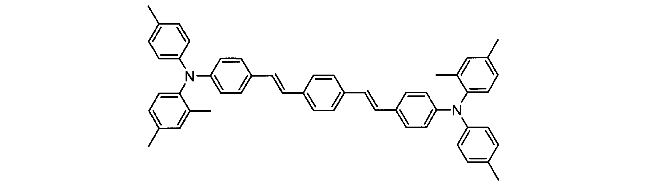
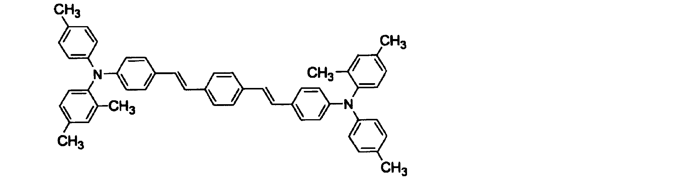
- Example 14 A photoconductor was prepared in the same manner as in Example 7 except that the charge transporting material used in Example 7 was changed to a compound represented by the following structural formula.
- Comparative Example 2 The copolymer polyarylate resin (III-1) of Production Example 1 used in Example 1 was replaced with the copolymer polyarylate resin (III-15) of Production Example 15 in the same manner as in Example 1. A photoconductor was prepared.
- Example 15 A vinyl chloride-vinyl acetate-vinyl alcohol copolymer (manufactured by Nissin Chemical Industry Co., Ltd., trade name “Solvine TA5R”) is used as the undercoat layer 2 on the outer periphery of an aluminum cylinder having an outer diameter of 24 mm as the conductive substrate 1. )
- the coating solution 4 prepared by stirring and dissolving 0.2 parts by mass in 99 parts by mass of methyl ethyl ketone was dip coated and dried at a temperature of 100 ° C. for 30 minutes to form an undercoat layer 2 having a thickness of 0.1 ⁇ m. .
- the following formula as a charge generation material 1 part by weight of a metal-free phthalocyanine represented by the following formula (II-1) as a hole transport material, 30 parts by mass of a stilbene compound represented by the following formula: 15 parts by mass of a stilbene compound represented by the following formula as an electron transport material:
- a coating solution 5 prepared by dissolving and dispersing 30 parts by mass of the compound represented by the formula (2) and 55 parts by mass of the copolymerized polyarylate resin (III-1) of Production Example 1 as a resin binder in 350 parts by mass of tetrahydrofuran. It was dip coated and dried at a temperature of 100 ° C. for 60 minutes to form a photosensitive layer 3 having a film thickness of 25 ⁇ m, and a single layer type photoreceptor was produced.
- Example 16 A photoconductor was prepared in the same manner as in Example 15 except that the stilbene compound (II-1) as the hole transport material used in Example 15 was changed to that represented by the following formula (II-8). .
- Example 17 Manufacture of positively charged laminated photoreceptor (Example 17) The following formula as a charge transport material: And 50 parts by mass of a Z-type polycarbonate (PCZ-500 manufactured by Mitsubishi Gas Chemical Co., Ltd.) as a resin binder were dissolved in 800 parts by mass of dichloromethane to prepare a coating solution 6. The coating liquid 6 was dip-coated on the outer periphery of an aluminum cylinder having an outer diameter of 24 mm as the conductive substrate 1 and dried at a temperature of 120 ° C. for 60 minutes to form a charge transport layer 5 having a thickness of 15 ⁇ m.
- a Z-type polycarbonate PCZ-500 manufactured by Mitsubishi Gas Chemical Co., Ltd.
- the following formula as a charge generation material 1.2 parts by mass of metal-free phthalocyanine represented by the following formula as a hole transport material, 10 parts by mass of a stilbene compound represented by the following formula as an electron transport material: And 60 parts by mass of the copolymer polyarylate resin (III-1) of Production Example 1 as a resin binder were dissolved and dispersed in 800 parts by mass of 1,2-dichloroethane.
- the coating liquid 7 was dip coated and dried at a temperature of 100 ° C. for 60 minutes to form a photosensitive layer 3 having a film thickness of 15 ⁇ m, and a positively charged laminated type photoreceptor was produced.
- exposure light of 1.0 ⁇ W / cm 2 spectrally split at 780 nm using a filter is irradiated to the photoconductor for 5 seconds from the time when the surface potential becomes ⁇ 600 V, and the surface potential is reduced.
- the exposure amount required for light attenuation until ⁇ 300 V was evaluated as E 1/2 ( ⁇ J / cm 2 ), and the residual potential on the surface of the photoreceptor 5 seconds after the exposure was evaluated as Vr 5 (V).
- the photoconductors produced in Examples 1 to 14 and Comparative Examples 1 to 5 were mounted on a printer LJ4250 made by HP Co., Ltd. modified so that the surface potential of the photoconductor could be measured, and 10,000 sheets of A4 paper were loaded. Printing was performed, and the film thickness of the photoconductor before and after printing was measured, and the amount of wear ( ⁇ m) after printing was evaluated. Further, the photoconductors produced in Examples 15 to 17 and Comparative Examples 6 and 7 were mounted on a printer HL-2040 manufactured by Brother Industries, Ltd., which was modified so that the surface potential of the photoconductor could be measured. The partial potential was evaluated. Furthermore, 10,000 A4 sheets were printed, the film thickness of the photoconductor before and after printing was measured, and the amount of wear ( ⁇ m) after printing was evaluated.
- the diameter (r) ( ⁇ ) and the helical interval (l) ( ⁇ ) of the helical structure are obtained from the molecular coordinates, and the value of r / l was calculated.
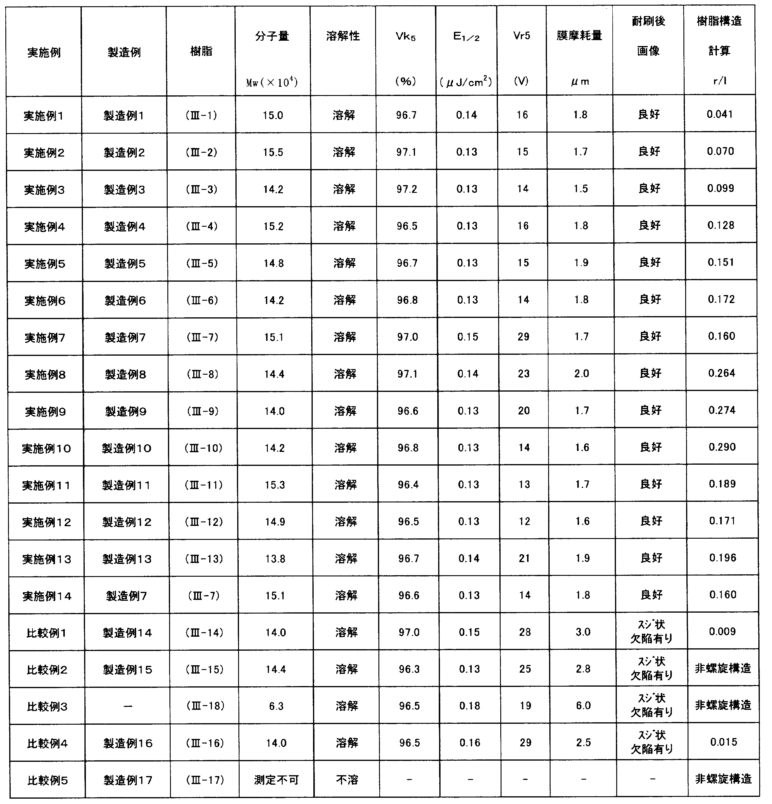
- the evaluation results are shown in Tables 2 and 3 below.
Landscapes
- Physics & Mathematics (AREA)
- General Physics & Mathematics (AREA)
- Spectroscopy & Molecular Physics (AREA)
- Chemical & Material Sciences (AREA)
- Chemical Kinetics & Catalysis (AREA)
- Photoreceptors In Electrophotography (AREA)
Abstract
Description
(化学構造式1)




上述のように、電子写真用感光体は、積層型(機能分離型)感光体としての、いわゆる負帯電積層型感光体および正帯電積層型感光体と、主として正帯電型で用いられる単層型感光体とに大別される。図1は、本発明の電子写真用感光体の一例を示す模式的断面図であり、(a)は負帯電型の積層型電子写真用感光体、(b)は正帯電型の単層型電子写真用感光体、(c)は正帯電型の積層型電子写真用感光体をそれぞれ示す。図示するように、負帯電積層型感光体においては、導電性基体1の上に、下引き層2と、電荷発生機能を備えた電荷発生層4および電荷輸送機能を備えた電荷輸送層5を有する感光層とが、順次積層されている。また、正帯電単層型感光体においては、導電性基体1の上に、下引き層2と、電荷発生および電荷輸送の両機能を併せ持つ単層型の感光層3とが、順次積層されている。さらに、正帯電積層型感光体においては、導電性基体1の上に、下引き層2と、電荷輸送機能を備えた電荷輸送層5、並びに、電荷発生および電荷輸送の両機能を備えた電荷発生層4を有する感光層とが、順次積層されている。なお、いずれのタイプの感光体においても、下引き層2は必要に応じ設ければよい。また、本発明の「感光層」は、電荷発生層および電荷輸送層を積層した積層型感光層と、単層型感光層との両方を含む。
負帯電積層型感光体において、電荷発生層4は、電荷発生材料の粒子が樹脂バインダ中に分散された塗布液を塗布するなどの方法により形成され、光を受容して電荷を発生する。電荷発生層4は、その電荷発生効率が高いことと同時に発生した電荷の電荷輸送層5への注入性が重要であり、電場依存性が少なく、低電場でも注入の良いことが望ましい。電荷発生材料としては、X型無金属フタロシアニン、τ型無金属フタロシアニン、α型チタニルフタロシアニン、β型チタニルフタロシアニン、Y型チタニルフタロシアニン、γ型チタニルフタロシアニン、アモルファス型チタニルフタロシアニン、ε型銅フタロシアニンなどのフタロシアニン化合物、各種アゾ顔料、アントアントロン顔料、チアピリリウム顔料、ペリレン顔料、ペリノン顔料、スクアリリウム顔料、キナクリドン顔料等を単独、または適宜組み合わせて用いることができ、画像形成に使用される露光光源の光波長領域に応じて好適な物質を選ぶことができる。なお、電荷発生層4における電荷発生材料の含有量は、電荷発生層4中の固形分に対して、好適には20~80質量%、より好適には30~70質量%である。














正帯電単層型感光体において、単層型感光層3は、主として電荷発生材料、正孔輸送材料、電子輸送材料(アクセプター性化合物)および樹脂バインダからなる。
正帯電積層型感光体において、電荷輸送層5は、主として電荷輸送材料と樹脂バインダとにより構成される。かかる電荷輸送材料および樹脂バインダとしては、負帯電積層型感光体の電荷輸送層5について挙げたものと同様の材料を用いることができる。各材料の含有量、および、電荷輸送層5の膜厚についても、負帯電積層型感光体と同様とすることができる。なお、本発明においては、正帯電積層型感光体の場合には、電荷輸送層5の樹脂バインダとして、上記螺旋構造を有する樹脂を任意に用いることができる。
本発明の電子写真用感光体は、各種マシンプロセスに適用することにより所期の効果が得られるものである。具体的には、ローラやブラシを用いた接触帯電方式、コロトロンやスコロトロンなどを用いた非接触帯電方式等の帯電プロセス、並びに、非磁性一成分、磁性一成分、二成分などの現像方式を用いた接触現像および非接触現像方式などの現像プロセスにおいても、十分な効果を得ることができる。
(製造例1)共重合ポリアリレート樹脂(III-1)の製造方法
2リットルの4口平底フラスコに、イオン交換水540mLと、NaOH12.4gと、p-tert-ブチルフェノール0.459gと、上記モノマーM1(2,6-ビス(4-ヒドロキシ-3-メチルフェニル)メタン)24.279gと、ビフェノール(以下、「BP」と称する。)4.95gと、テトラブチルアンモニウムブロミド0.272gとを仕込んで、溶液(i)を作製した。次いで、脱水塩化メチレン540mlに、テレフタル酸クロライド12.27gと、イソフタル酸クロライド14.99gとを溶解した溶液(ii)を作製した。まず、溶液(i)を溶液(ii)に滴下し、2時間攪拌して、反応を行った。反応終了後、酢酸4.74mLで中和し、塩化メチレン360mLを追加して希釈した。水相を分離し、これを4倍容量のメタノールにて再沈した。60℃で2時間乾燥させた後、得られた生成物を塩化メチレンにて5%溶液にし、それを3Lのイオン交換水中に加えて、樹脂を再沈させることにより洗浄した。この洗浄を、洗浄水の導電率が1μS/m以下となるまで実施した。取り出した樹脂を、再度、塩化メチレンに5質量%で溶解し、攪拌している5倍量のアセトン中に滴下させて、再沈を行った。析出物をろ過し、60℃で2時間乾燥して、目的のポリマー42.24gを得た。この共重合ポリアリレート樹脂(III-1)の、THF-d8溶媒中の1H―NMRスペクトルを図3に示し、共重合比を以下に示す。
a:b:c:d=36.0:44.0:9.0:11.0
この共重合ポリアリレート樹脂(III-1)のポリスチレン換算重量平均分子量を
GPC分析により測定したところ、分子量は150000であった。
製造例1中の、モノマーM1をM2に変更し、27.262gを加えることとした以外は製造例1と同様にして、合成を実施した。得られた共重合ポリアリレート樹脂を(III-2)とする。
製造例1中の、モノマーM1をM3に変更し、30.245gを加えることとした以外は製造例1と同様にして、合成を実施した。得られた共重合ポリアリレート樹脂を(III-3)とする。
製造例1中の、モノマーM1をM4に変更し、33.229gを加えることとした以外は製造例1と同様にして、合成を実施した。得られた共重合ポリアリレート樹脂を(III-4)とする。
製造例1中の、モノマーM1をM5に変更し、36.212gを加えることとした以外は製造例1と同様にして、合成を実施した。得られた共重合ポリアリレート樹脂を(III-5)とする。
製造例1中の、モノマーM1をM6に変更し、45.163gを加えることとした以外は製造例1と同様にして、合成を実施した。得られた共重合ポリアリレート樹脂を(III-6)とする。
製造例1中の、モノマーM1をM7に変更し、33.229gを加えることとした以外は製造例1と同様にして、合成を実施した。得られた共重合ポリアリレート樹脂を(III-7)とする。
製造例1中の、モノマーM1をM8に変更し、37.481gを加えることとした以外は製造例1と同様にして、合成を実施した。得られた共重合ポリアリレート樹脂を(III-8)とする。
製造例1中の、モノマーM1をM9に変更し、53.667gを加えることとした以外は製造例1と同様にして、合成を実施した。得られた共重合ポリアリレート樹脂を(III-9)とする。
製造例1中の、モノマーM1をM10に変更し、69.852gを加えることとした以外は製造例1と同様にして、合成を実施した。得られた共重合ポリアリレート樹脂を(III-10)とする。
製造例1中の、モノマーM1をM11に変更し、38.767gを加えることとした以外は製造例1と同様にして、合成を実施した。得られた共重合ポリアリレート樹脂を(III-11)とする。
製造例7中の、モノマーM7を37.383gとし、BPを2.48gとした以外は製造例7と同様にして、合成を実施した。得られた共重合ポリアリレート樹脂を(III-12)とする。
製造例7中の、モノマーM7を41.536gとし、BPを添加しない以外は製造例7と同様にして、合成を実施した。得られた共重合ポリアリレート樹脂を(III-13)とする。
製造例13中の、モノマーM7を下記のモノマーM13とし、30.348gを添加した以外は製造例13と同様にして、合成を実施した。得られた共重合ポリアリレート樹脂を(III-14)とする。

製造例13中の、モノマーM7を下記のモノマーM14とし、26.618gを添加した以外は製造例13と同様にして、合成を実施した。得られた共重合ポリアリレート樹脂を(III-15)とする。

製造例7中の、モノマーM7を24.922gとし、BPを9.90gとした以外は製造例7と同様にして、合成を実施した。得られた共重合ポリアリレート樹脂を(III-16)とする。
製造例7中の、モノマーM7を20.768gとし、BPを12.38gとした以外は製造例7と同様にして、合成を実施した。得られた共重合ポリアリレート樹脂を(III-17)とする。
(実施例1)
アルコール可溶性ナイロン(東レ(株)製、商品名「CM8000」)5質量部と、アミノシラン処理された酸化チタン微粒子5質量部とを、メタノール90質量部に溶解、分散させて、塗布液1を調製した。導電性基体1としての外径30mmのアルミニウム製円筒の外周に、下引き層2として、この塗布液1を浸漬塗工し、温度100℃で30分間乾燥して、膜厚3μmの下引き層2を形成した。
実施例1で使用した製造例1の共重合ポリアリレート樹脂(III-1)を、製造例2の共重合ポリアリレート樹脂(III-2)に変えた以外は、実施例1と同様の方法で感光体を作製した。
実施例1で使用した製造例1の共重合ポリアリレート樹脂(III-1)を、製造例3の共重合ポリアリレート樹脂(III-3)に変えた以外は、実施例1と同様の方法で感光体を作製した。
実施例1で使用した製造例1の共重合ポリアリレート樹脂(III-1)を、製造例4の共重合ポリアリレート樹脂(III-4)に変えた以外は、実施例1と同様の方法で感光体を作製した。
実施例1で使用した製造例1の共重合ポリアリレート樹脂(III-1)を、製造例5の共重合ポリアリレート樹脂(III-5)に変えた以外は、実施例1と同様の方法で感光体を作製した。
実施例1で使用した製造例1の共重合ポリアリレート樹脂(III-1)を、製造例6の共重合ポリアリレート樹脂(III-6)に変えた以外は、実施例1と同様の方法で感光体を作製した。
実施例1で使用した製造例1の共重合ポリアリレート樹脂(III-1)を、製造例7の共重合ポリアリレート樹脂(III-7)に変えた以外は、実施例1と同様の方法で感光体を作製した。
実施例1で使用した製造例1の共重合ポリアリレート樹脂(III-1)を、製造例8の共重合ポリアリレート樹脂(III-8)に変えた以外は、実施例1と同様の方法で感光体を作製した。
実施例1で使用した製造例1の共重合ポリアリレート樹脂(III-1)を、製造例9の共重合ポリアリレート樹脂(III-9)に変えた以外は、実施例1と同様の方法で感光体を作製した。
実施例1で使用した製造例1の共重合ポリアリレート樹脂(III-1)を、製造例10の共重合ポリアリレート樹脂(III-10)に変えた以外は、実施例1と同様の方法で感光体を作製した。
実施例1で使用した製造例1の共重合ポリアリレート樹脂(III-1)を、製造例11の共重合ポリアリレート樹脂(III-11)に変えた以外は、実施例1と同様の方法で感光体を作製した。
実施例1で使用した製造例1の共重合ポリアリレート樹脂(III-1)を、製造例12の共重合ポリアリレート樹脂(III-12)に変えた以外は、実施例1と同様の方法で感光体を作製した。
実施例1で使用した製造例1の共重合ポリアリレート樹脂(III-1)を、製造例13の共重合ポリアリレート樹脂(III-13)に変えた以外は、実施例1と同様の方法で感光体を作製した。
実施例7で使用した電荷輸送材料を下記構造式で示される化合物に変えた以外は、実施例7と同様の方法で感光体を作製した。

実施例1で使用した製造例1の共重合ポリアリレート樹脂(III-1)を、製造例14の共重合ポリアリレート樹脂(III-14)に変えた以外は、実施例1と同様の方法で感光体を作製した。
実施例1で使用した製造例1の共重合ポリアリレート樹脂(III-1)を、製造例15の共重合ポリアリレート樹脂(III-15)に変えた以外は、実施例1と同様の方法で感光体を作製した。
実施例1で使用した製造例1の共重合ポリアリレート樹脂(III-1)を、ポリカーボネート樹脂A(三菱エンジニアリングプラスチック(株)製、S-3000)(以下、「III-18」と称する)に変えた以外は、実施例1と同様の方法で感光体を作製した。
実施例1で使用した製造例1の共重合ポリアリレート樹脂(III-1)を、製造例16の共重合ポリアリレート樹脂(III-16)に変えた以外は、実施例1と同様の方法で感光体を作製した。
実施例1で使用した製造例1の共重合ポリアリレート樹脂(III-1)を、製造例17の共重合ポリアリレート樹脂(III-17)に変えた以外は、実施例1と同様の方法で感光体を作製した。
(実施例15)
導電性基体1としての外径24mmのアルミニウム製円筒の外周に、下引き層2として、塩化ビニル-酢酸ビニル-ビニルアルコール共重合体(日信化学工業(株)製、商品名「ソルバインTA5R」)0.2質量部をメチルエチルケトン99質量部に攪拌溶解させて調製した塗布液4を浸漬塗工し、温度100℃で30分間乾燥して、膜厚0.1μmの下引き層2を形成した。


実施例15で使用した正孔輸送材料としてのスチルベン化合物(II-1)を下記式(II-8)で示されるものに変えた以外は、実施例15と同様の方法で感光体を作製した。

実施例16で使用した製造例1の共重合ポリアリレート樹脂(III-1)を、製造例16の共重合ポリアリレート樹脂(III-16)に変えた以外は、実施例16と同様の方法で感光体を作製した。
(実施例17)
電荷輸送材料としての下記式、

で示される無金属フタロシアニン1.2質量部と、正孔輸送材料としての下記式、

で示されるスチルベン化合物10質量部と、電子輸送材料としての下記式、
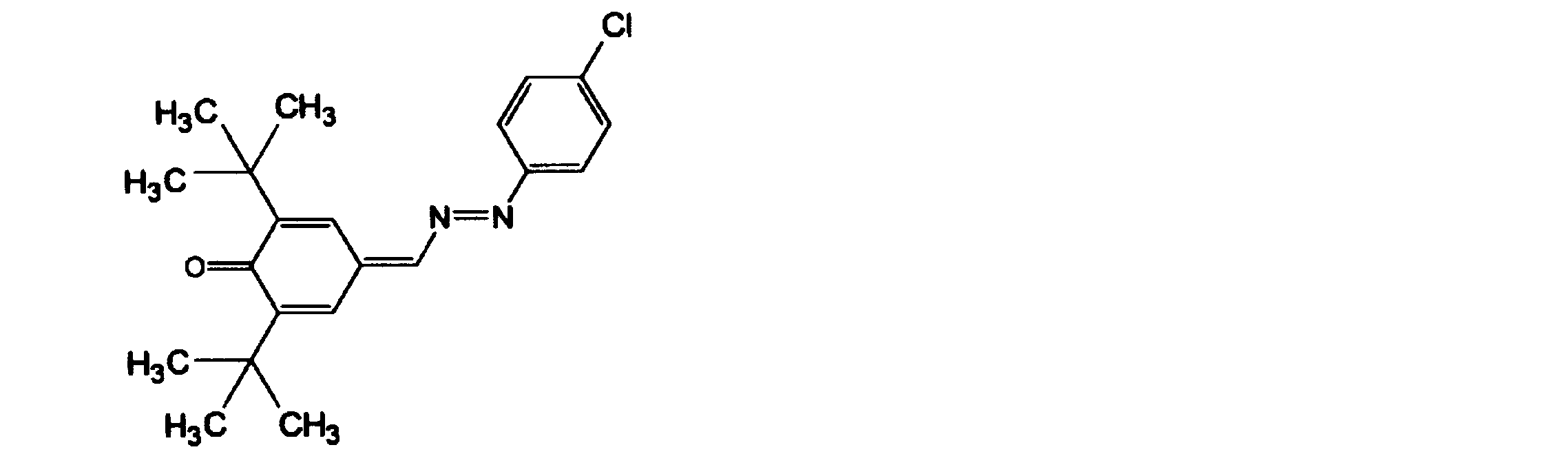
実施例17で使用した製造例1の共重合ポリアリレート樹脂(III‐1)を製造例16の共重合ポリアリレート樹脂(III-16)に変えた以外は、実施例17と同様の方法で感光体を作製した。
上述した実施例1~17および比較例1~7で作製した感光体の電気特性を、下記の方法で評価した。併せて、塗布液状態の評価として、電荷輸送層用塗布液調製時における樹脂バインダの溶剤に対する溶解性についても評価した。
各実施例および比較例にて得られた感光体の電気特性を、ジェンテック社製のプロセスシミュレーター(CYNTHIA91)を使用して、以下の方法で評価した。実施例1~17および比較例1~7の感光体について、温度22℃、湿度50%の環境下で、感光体の表面を暗所にてコロナ放電により-650Vに帯電せしめた後、帯電直後の表面電位V0を測定した。続いて、暗所で5秒間放置後、表面電位V5を測定し、下記計算式(1)、
Vk5=V5/V0×100 (1)
に従って、帯電後5秒後における電位保持率Vk5(%)を求めた。次に、ハロゲンランプを光源とし、フィルターを用いて780nmに分光した1.0μW/cm2の露光光を、表面電位が-600Vになった時点から感光体に5秒間照射して、表面電位が-300Vとなるまで光減衰するのに要する露光量をE1/2(μJ/cm2)、露光後5秒後の感光体表面の残留電位をVr5(V)として評価した。
実施例1~14および比較例1~5において作製した感光体を、感光体の表面電位も測定できるように改造を施したHP(株)製のプリンターLJ4250に搭載して、A4用紙10000枚を印字し、印字前後の感光体の膜厚を測定して、印字後の摩耗量(μm)について評価を実施した。また、実施例15~17および比較例6,7において作製した感光体を、感光体の表面電位も測定できるように改造を施したブラザー工業(株)製のプリンターHL-2040に搭載して露光部電位を評価した。さらに、A4用紙10000枚を印字し、印字前後の感光体の膜厚を測定して、印字後の摩耗量(μm)について評価を実施した。
各製造例で製造した樹脂の構造について、構成モノマーの重合時の仕込みmol比率を基にして、樹脂の構造最適化計算を行った。構造最適化計算はJ-OCTA(JSOL社製)の分子動力学シミュレーションプログラムであるCOGNACを使用し、全原子モデルにて樹脂構造を形成し、力場パラメータとしてDreiding Modelを選択、温度条件を300K、最大繰返し回数10000、収束判定値を1%として、RIS Monte Carlo計算により、最適化3次元分子構造(安定構造)とした。繰返しモノマー数としては、総原子数が10000個を超える最低繰返し数とした。
得られたポリマーの分子構造が螺旋状構造をとった場合、その分子座標から、螺旋構造の直径(r)(Å)と螺旋間隔(l)(Å)とを求めて、r/lの値を算出した。これらの評価結果を、下記表2,3に示す。

2 下引き層
3 単層型感光層
4 電荷発生層
5 電荷輸送層
7 感光体
21 ローラ帯電部材
22 高圧電源
23 像露光部材
24 現像器
241 現像ローラ
25 給紙部材
251 給紙ローラ
252 給紙ガイド
26 転写帯電器(直接帯電型)
27 クリーニング装置
271 クリーニングブレード
28 除電部材
60 電子写真装置
300 感光層
Claims (14)
- 導電性基体上に感光層を有する電子写真用感光体において、
前記感光層が、分子動力学計算を用いて最適化された分子構造が螺旋構造である樹脂を含有し、かつ、該樹脂の、螺旋構造の直径(r)と螺旋間隔(l)との比r/lの値が、0.04以上1.0以下の範囲であることを特徴とする電子写真用感光体。 - 前記樹脂が、ポリカーボネート樹脂またはポリアリレート樹脂である請求項1記載の電子写真用感光体。
- 前記ポリアリレート樹脂が、下記化学構造式1で表される繰り返し単位を有する請求項2記載の電子写用真感光体。
(化学構造式1)


 (化学構造式1中、部分構造式(A)、(B)、(C)および(D)はそれぞれ、樹脂を構成する構造単位を示し、a、b、cおよびdはそれぞれ各構造単位(A)、(B)、(C)および(D)のmol%を示し、a+b+c+dは100mol%であり、R1およびR2は、同一でも異なっていてもよく、炭素数1~8のアルキル基、置換基を有してもよいシクロアルキル基、または、置換基を有してもよいアリール基を示し、R3およびR4は、同一でも異なっていてもよく、水素原子、炭素数1~8のアルキル基、置換基を有してもよいシクロアルキル基、若しくは、置換基を有してもよいアリール基を示し、または、R3およびR4は、それらが結合している炭素原子と共に環状構造を形成していてもよく、この環状構造には1または2個のアリーレン基が結合していてもよい)
- 前記化学構造式1中、cおよびdが0mol%である請求項3記載の電子写真用感光体。
- 前記化学構造式1中、a+bが65mol%以上100mol%未満である請求項3記載の電子写真用感光体。
- 前記感光層が少なくとも電荷発生層と電荷輸送層とを備え、かつ、該電荷輸送層が、前記樹脂と電荷輸送材料とを含む請求項1記載の電子写真用感光体。
- 前記電荷発生層と前記電荷輸送層とが、この順に前記導電性基体上に積層されてなる請求項6記載の電子写真用感光体。
- 前記感光層が、前記樹脂と、電荷発生材料および電荷輸送材料とを含む請求項1記載の電子写真用感光体。
- 前記感光層が少なくとも電荷輸送層と電荷発生層とを備え、かつ、該電荷発生層が、前記樹脂と、電荷発生材料および電荷輸送材料とを含む請求項1記載の電子写真用感光体。
- 前記電荷輸送層と前記電荷発生層とが、この順に前記導電性基体上に積層されてなる請求項9記載の電子写真用感光体。
- 前記電荷輸送材料が正孔輸送材料と電子輸送材料とを含む請求項8記載の電子写真用感光体。
- 導電性基体上に、少なくとも樹脂バインダを含む塗布液を塗布して感光層を形成する工程を包含する電子写真用感光体の製造方法において、該樹脂バインダが、分子動力学計算を用いて最適化された分子構造が螺旋構造である樹脂を含有し、かつ、該樹脂の、螺旋構造の直径(r)と螺旋間隔(l)との比r/lの値が、0.04以上1.0以下の範囲であることを特徴とする電子写真用感光体の製造方法。
- 前記樹脂として、下記化学構造式1で表される繰り返し単位を有するものを用いる請求項12記載の電子写真用感光体の製造方法。
(化学構造式1)


 (化学構造式1中、部分構造式(A)、(B)、(C)および(D)はそれぞれ、樹脂を構成する構造単位を示し、a、b、cおよびdはそれぞれ各構造単位(A)、(B)、(C)および(D)のmol%を示し、a+b+c+dは100mol%であり、R1およびR2は、同一でも異なっていてもよく、炭素数1~8のアルキル基、置換基を有してもよいシクロアルキル基、または、置換基を有してもよいアリール基を示し、R3およびR4は、同一でも異なっていてもよく、水素原子、炭素数1~8のアルキル基、置換基を有してもよいシクロアルキル基、若しくは、置換基を有してもよいアリール基を示し、または、R3およびR4は、それらが結合している炭素原子と共に環状構造を形成していてもよく、この環状構造には1または2個のアリーレン基が結合していてもよい)
- 請求項1記載の電子写真用感光体を搭載したことを特徴とする電子写真装置。
Priority Applications (6)
| Application Number | Priority Date | Filing Date | Title |
|---|---|---|---|
| KR1020167003510A KR20160103970A (ko) | 2013-12-27 | 2013-12-27 | 전자 사진용 감광체, 그 제조방법 및 전자 사진 장치 |
| CN201380078881.2A CN105531629B (zh) | 2013-12-27 | 2013-12-27 | 电子照相用感光体、其制造方法及电子照相装置 |
| PCT/JP2013/085250 WO2015097903A1 (ja) | 2013-12-27 | 2013-12-27 | 電子写真用感光体、その製造方法および電子写真装置 |
| JP2015554478A JP6107973B2 (ja) | 2013-12-27 | 2013-12-27 | 電子写真用感光体、その製造方法および電子写真装置 |
| TW103143900A TWI632171B (zh) | 2013-12-27 | 2014-12-16 | 電子照相用感光體、其製造方法及電子照相裝置 |
| US15/042,131 US9703215B2 (en) | 2013-12-27 | 2016-02-11 | Electrophotographic photoreceptor, method of producing same, and electrophotographic apparatus |
Applications Claiming Priority (1)
| Application Number | Priority Date | Filing Date | Title |
|---|---|---|---|
| PCT/JP2013/085250 WO2015097903A1 (ja) | 2013-12-27 | 2013-12-27 | 電子写真用感光体、その製造方法および電子写真装置 |
Related Child Applications (1)
| Application Number | Title | Priority Date | Filing Date |
|---|---|---|---|
| US15/042,131 Continuation US9703215B2 (en) | 2013-12-27 | 2016-02-11 | Electrophotographic photoreceptor, method of producing same, and electrophotographic apparatus |
Publications (1)
| Publication Number | Publication Date |
|---|---|
| WO2015097903A1 true WO2015097903A1 (ja) | 2015-07-02 |
Family
ID=53477830
Family Applications (1)
| Application Number | Title | Priority Date | Filing Date |
|---|---|---|---|
| PCT/JP2013/085250 Ceased WO2015097903A1 (ja) | 2013-12-27 | 2013-12-27 | 電子写真用感光体、その製造方法および電子写真装置 |
Country Status (6)
| Country | Link |
|---|---|
| US (1) | US9703215B2 (ja) |
| JP (1) | JP6107973B2 (ja) |
| KR (1) | KR20160103970A (ja) |
| CN (1) | CN105531629B (ja) |
| TW (1) | TWI632171B (ja) |
| WO (1) | WO2015097903A1 (ja) |
Cited By (7)
| Publication number | Priority date | Publication date | Assignee | Title |
|---|---|---|---|---|
| WO2017170615A1 (ja) * | 2016-03-29 | 2017-10-05 | 三菱化学株式会社 | 正帯電用電子写真感光体、電子写真感光体カートリッジ、及び画像形成装置 |
| JP2018189941A (ja) * | 2017-04-28 | 2018-11-29 | 京セラドキュメントソリューションズ株式会社 | 電子写真感光体、プロセスカートリッジ及び画像形成装置 |
| JP2020060663A (ja) * | 2018-10-09 | 2020-04-16 | 富士電機株式会社 | 電子写真用感光体およびそれを搭載した電子写真装置 |
| JP2021021756A (ja) * | 2019-07-24 | 2021-02-18 | 富士電機株式会社 | 電子写真用感光体、その製造方法およびそれを搭載した電子写真装置 |
| JP2021033211A (ja) * | 2019-08-29 | 2021-03-01 | 株式会社沖データ | 像担持体ユニットおよび画像形成装置 |
| JP7567660B2 (ja) | 2021-05-26 | 2024-10-16 | 京セラドキュメントソリューションズ株式会社 | 電子写真感光体 |
| JP7571802B2 (ja) | 2021-01-26 | 2024-10-23 | 京セラドキュメントソリューションズ株式会社 | ポリアリレート樹脂、及び電子写真感光体 |
Families Citing this family (2)
| Publication number | Priority date | Publication date | Assignee | Title |
|---|---|---|---|---|
| US10739705B2 (en) | 2016-08-10 | 2020-08-11 | Ball Corporation | Method and apparatus of decorating a metallic container by digital printing to a transfer blanket |
| RU2757163C1 (ru) * | 2018-02-09 | 2021-10-11 | Бол Корпорейшн | Способ и устройство для декорирования металлического контейнера с помощью цифровой печати на офсетном полотне |
Citations (5)
| Publication number | Priority date | Publication date | Assignee | Title |
|---|---|---|---|---|
| JPH036567A (ja) * | 1989-06-02 | 1991-01-14 | Kanegafuchi Chem Ind Co Ltd | 電子写真感光体 |
| JPH10504311A (ja) * | 1994-08-20 | 1998-04-28 | ビーエーエスエフ アクチェンゲゼルシャフト | 円柱状螺旋相を成し、液晶特性を有する低分子量もしくは高分子有機化合物の用途 |
| JP2002251024A (ja) * | 2001-02-22 | 2002-09-06 | Canon Inc | 電子写真感光体、プロセスカートリッジ及び電子写真装置 |
| JP2003082078A (ja) * | 2001-06-29 | 2003-03-19 | Mitsubishi Chemicals Corp | ポリエステル樹脂およびそれを用いた電子写真感光体 |
| JP2005173376A (ja) * | 2003-12-12 | 2005-06-30 | Fuji Xerox Co Ltd | 電子写真感光体及びその製造方法、プロセスカートリッジ並びに画像形成装置 |
Family Cites Families (18)
| Publication number | Priority date | Publication date | Assignee | Title |
|---|---|---|---|---|
| JPS6162040A (ja) | 1984-09-04 | 1986-03-29 | Fuji Xerox Co Ltd | 電子写真用感光体 |
| JPH01205171A (ja) | 1988-02-10 | 1989-08-17 | Ricoh Co Ltd | 電子写真感光体 |
| JPH07333881A (ja) | 1994-06-13 | 1995-12-22 | Canon Inc | 電子写真感光体及び該電子写真感光体を備えた電子写真装置 |
| JPH08209023A (ja) | 1994-11-24 | 1996-08-13 | Fuji Electric Co Ltd | チタニルオキシフタロシアニン結晶とその製法及び電子写真感光体 |
| US5874570A (en) | 1995-11-10 | 1999-02-23 | Fuji Electric Co., Ltd. | Titanyloxyphthalocyanine crystals, and method of preparing the same |
| JP2000292957A (ja) * | 1999-04-12 | 2000-10-20 | Canon Inc | 電子写真感光体、プロセスカートリッジ及び電子写真装置 |
| JP4100815B2 (ja) * | 1999-04-12 | 2008-06-11 | キヤノン株式会社 | 電子写真感光体、プロセスカートリッジ及び電子写真装置 |
| JP4217362B2 (ja) * | 2000-01-19 | 2009-01-28 | キヤノン株式会社 | 電子写真感光体、並びに、該電子写真感光体を備えたプロセスカートリッジおよび電子写真装置 |
| JP3781268B2 (ja) | 2000-10-25 | 2006-05-31 | 三菱化学株式会社 | ポリエステル樹脂及びその製造方法、並びにそれを用いた電子写真感光体 |
| JP2002214807A (ja) | 2001-01-17 | 2002-07-31 | Mitsubishi Chemicals Corp | 電子写真感光体 |
| JP3740450B2 (ja) | 2002-08-30 | 2006-02-01 | キヤノン株式会社 | 電子写真装置 |
| JP4336559B2 (ja) | 2003-10-08 | 2009-09-30 | 富士電機デバイステクノロジー株式会社 | 電子写真用感光体およびその製造方法 |
| JP2007093733A (ja) * | 2005-09-27 | 2007-04-12 | Canon Inc | 電子写真感光体、プロセスカートリッジ及び電子写真装置 |
| JP4550718B2 (ja) | 2005-10-28 | 2010-09-22 | 京セラミタ株式会社 | 電子写真感光体 |
| JP4663768B2 (ja) * | 2008-04-15 | 2011-04-06 | シャープ株式会社 | 電子写真感光体を備えた画像形成装置 |
| JP5077765B2 (ja) | 2008-04-30 | 2012-11-21 | 富士電機株式会社 | 電子写真用感光体およびその製造方法 |
| JP5481829B2 (ja) | 2008-10-16 | 2014-04-23 | 三菱化学株式会社 | 電子写真感光体、並びにそれを備えたカートリッジ及び画像形成装置 |
| CN105612461B (zh) * | 2012-02-28 | 2019-11-08 | 富士电机株式会社 | 电子照相用感光体、其制造方法和电子照相装置、以及共聚聚芳酯树脂的制造方法 |
-
2013
- 2013-12-27 WO PCT/JP2013/085250 patent/WO2015097903A1/ja not_active Ceased
- 2013-12-27 JP JP2015554478A patent/JP6107973B2/ja not_active Expired - Fee Related
- 2013-12-27 CN CN201380078881.2A patent/CN105531629B/zh not_active Expired - Fee Related
- 2013-12-27 KR KR1020167003510A patent/KR20160103970A/ko not_active Abandoned
-
2014
- 2014-12-16 TW TW103143900A patent/TWI632171B/zh not_active IP Right Cessation
-
2016
- 2016-02-11 US US15/042,131 patent/US9703215B2/en not_active Expired - Fee Related
Patent Citations (5)
| Publication number | Priority date | Publication date | Assignee | Title |
|---|---|---|---|---|
| JPH036567A (ja) * | 1989-06-02 | 1991-01-14 | Kanegafuchi Chem Ind Co Ltd | 電子写真感光体 |
| JPH10504311A (ja) * | 1994-08-20 | 1998-04-28 | ビーエーエスエフ アクチェンゲゼルシャフト | 円柱状螺旋相を成し、液晶特性を有する低分子量もしくは高分子有機化合物の用途 |
| JP2002251024A (ja) * | 2001-02-22 | 2002-09-06 | Canon Inc | 電子写真感光体、プロセスカートリッジ及び電子写真装置 |
| JP2003082078A (ja) * | 2001-06-29 | 2003-03-19 | Mitsubishi Chemicals Corp | ポリエステル樹脂およびそれを用いた電子写真感光体 |
| JP2005173376A (ja) * | 2003-12-12 | 2005-06-30 | Fuji Xerox Co Ltd | 電子写真感光体及びその製造方法、プロセスカートリッジ並びに画像形成装置 |
Cited By (10)
| Publication number | Priority date | Publication date | Assignee | Title |
|---|---|---|---|---|
| WO2017170615A1 (ja) * | 2016-03-29 | 2017-10-05 | 三菱化学株式会社 | 正帯電用電子写真感光体、電子写真感光体カートリッジ、及び画像形成装置 |
| JPWO2017170615A1 (ja) * | 2016-03-29 | 2019-02-07 | 三菱ケミカル株式会社 | 正帯電用電子写真感光体、電子写真感光体カートリッジ、及び画像形成装置 |
| JP2018189941A (ja) * | 2017-04-28 | 2018-11-29 | 京セラドキュメントソリューションズ株式会社 | 電子写真感光体、プロセスカートリッジ及び画像形成装置 |
| JP2020060663A (ja) * | 2018-10-09 | 2020-04-16 | 富士電機株式会社 | 電子写真用感光体およびそれを搭載した電子写真装置 |
| JP7187958B2 (ja) | 2018-10-09 | 2022-12-13 | 富士電機株式会社 | 電子写真用感光体およびそれを搭載した電子写真装置 |
| JP2021021756A (ja) * | 2019-07-24 | 2021-02-18 | 富士電機株式会社 | 電子写真用感光体、その製造方法およびそれを搭載した電子写真装置 |
| JP7346974B2 (ja) | 2019-07-24 | 2023-09-20 | 富士電機株式会社 | 電子写真用感光体、その製造方法およびそれを搭載した電子写真装置 |
| JP2021033211A (ja) * | 2019-08-29 | 2021-03-01 | 株式会社沖データ | 像担持体ユニットおよび画像形成装置 |
| JP7571802B2 (ja) | 2021-01-26 | 2024-10-23 | 京セラドキュメントソリューションズ株式会社 | ポリアリレート樹脂、及び電子写真感光体 |
| JP7567660B2 (ja) | 2021-05-26 | 2024-10-16 | 京セラドキュメントソリューションズ株式会社 | 電子写真感光体 |
Also Published As
| Publication number | Publication date |
|---|---|
| CN105531629B (zh) | 2019-11-08 |
| JP6107973B2 (ja) | 2017-04-05 |
| JPWO2015097903A1 (ja) | 2017-03-23 |
| US20160161870A1 (en) | 2016-06-09 |
| TWI632171B (zh) | 2018-08-11 |
| KR20160103970A (ko) | 2016-09-02 |
| US9703215B2 (en) | 2017-07-11 |
| CN105531629A (zh) | 2016-04-27 |
| TW201546113A (zh) | 2015-12-16 |
Similar Documents
| Publication | Publication Date | Title |
|---|---|---|
| JP6107973B2 (ja) | 電子写真用感光体、その製造方法および電子写真装置 | |
| US9880477B2 (en) | Electrophotographic photoreceptor and image forming apparatus | |
| JP6741165B2 (ja) | 電子写真用感光体、その製造方法および電子写真装置 | |
| JP5195938B2 (ja) | 電子写真用感光体、その製造方法および電子写真装置 | |
| WO2011092850A1 (ja) | 電子写真用感光体、その製造方法および電子写真装置 | |
| JP4336559B2 (ja) | 電子写真用感光体およびその製造方法 | |
| KR101645781B1 (ko) | 전자사진용 감광체 및 그 제조 방법 | |
| JP5077765B2 (ja) | 電子写真用感光体およびその製造方法 | |
| JP2010107923A (ja) | 電子写真感光体及び電子写真装置 | |
| KR101525655B1 (ko) | 전자 사진용 감광체 및 그의 제조 방법 | |
| JP2001142235A (ja) | 電子写真用感光体 | |
| US8846279B2 (en) | Electrophotographic photoreceptor, electrophotographic photoreceptor cartridge and image forming apparatus | |
| JP3870184B2 (ja) | 電子写真用感光体 | |
| JP2003255569A (ja) | 単層型電子写真感光体、及びそれを使用した画像形成装置 | |
| JP4411232B2 (ja) | 電子写真感光体の製造方法 | |
| JP6597658B2 (ja) | 電子写真感光体、画像形成装置及びプロセスカートリッジ | |
| JP4538360B2 (ja) | 湿式現像用電子写真感光体および湿式現像用画像形成装置 | |
| JPH10186687A (ja) | 電子写真感光体、プロセスカートリッジ及び電子写真装置 |
Legal Events
| Date | Code | Title | Description |
|---|---|---|---|
| WWE | Wipo information: entry into national phase |
Ref document number: 201380078881.2 Country of ref document: CN |
|
| 121 | Ep: the epo has been informed by wipo that ep was designated in this application |
Ref document number: 13900396 Country of ref document: EP Kind code of ref document: A1 |
|
| ENP | Entry into the national phase |
Ref document number: 2015554478 Country of ref document: JP Kind code of ref document: A |
|
| ENP | Entry into the national phase |
Ref document number: 20167003510 Country of ref document: KR Kind code of ref document: A |
|
| NENP | Non-entry into the national phase |
Ref country code: DE |
|
| 122 | Ep: pct application non-entry in european phase |
Ref document number: 13900396 Country of ref document: EP Kind code of ref document: A1 |