WO2015056487A1 - インプリント法によるポリイミドの微細パターン形成方法 - Google Patents
インプリント法によるポリイミドの微細パターン形成方法 Download PDFInfo
- Publication number
- WO2015056487A1 WO2015056487A1 PCT/JP2014/072804 JP2014072804W WO2015056487A1 WO 2015056487 A1 WO2015056487 A1 WO 2015056487A1 JP 2014072804 W JP2014072804 W JP 2014072804W WO 2015056487 A1 WO2015056487 A1 WO 2015056487A1
- Authority
- WO
- WIPO (PCT)
- Prior art keywords
- polyimide
- pattern
- fine pattern
- solvent
- forming
- Prior art date
- Legal status (The legal status is an assumption and is not a legal conclusion. Google has not performed a legal analysis and makes no representation as to the accuracy of the status listed.)
- Ceased
Links
Images




Classifications
-
- B—PERFORMING OPERATIONS; TRANSPORTING
- B29—WORKING OF PLASTICS; WORKING OF SUBSTANCES IN A PLASTIC STATE IN GENERAL
- B29C—SHAPING OR JOINING OF PLASTICS; SHAPING OF MATERIAL IN A PLASTIC STATE, NOT OTHERWISE PROVIDED FOR; AFTER-TREATMENT OF THE SHAPED PRODUCTS, e.g. REPAIRING
- B29C59/00—Surface shaping of articles, e.g. embossing; Apparatus therefor
- B29C59/02—Surface shaping of articles, e.g. embossing; Apparatus therefor by mechanical means, e.g. pressing
- B29C59/022—Surface shaping of articles, e.g. embossing; Apparatus therefor by mechanical means, e.g. pressing characterised by the disposition or the configuration, e.g. dimensions, of the embossments or the shaping tools therefor
-
- G—PHYSICS
- G03—PHOTOGRAPHY; CINEMATOGRAPHY; ANALOGOUS TECHNIQUES USING WAVES OTHER THAN OPTICAL WAVES; ELECTROGRAPHY; HOLOGRAPHY
- G03F—PHOTOMECHANICAL PRODUCTION OF TEXTURED OR PATTERNED SURFACES, e.g. FOR PRINTING, FOR PROCESSING OF SEMICONDUCTOR DEVICES; MATERIALS THEREFOR; ORIGINALS THEREFOR; APPARATUS SPECIALLY ADAPTED THEREFOR
- G03F7/00—Photomechanical, e.g. photolithographic, production of textured or patterned surfaces, e.g. printing surfaces; Materials therefor, e.g. comprising photoresists; Apparatus specially adapted therefor
- G03F7/0002—Lithographic processes using patterning methods other than those involving the exposure to radiation, e.g. by stamping
-
- B—PERFORMING OPERATIONS; TRANSPORTING
- B29—WORKING OF PLASTICS; WORKING OF SUBSTANCES IN A PLASTIC STATE IN GENERAL
- B29C—SHAPING OR JOINING OF PLASTICS; SHAPING OF MATERIAL IN A PLASTIC STATE, NOT OTHERWISE PROVIDED FOR; AFTER-TREATMENT OF THE SHAPED PRODUCTS, e.g. REPAIRING
- B29C35/00—Heating, cooling or curing, e.g. crosslinking or vulcanising; Apparatus therefor
- B29C35/02—Heating or curing, e.g. crosslinking or vulcanizing during moulding, e.g. in a mould
- B29C35/08—Heating or curing, e.g. crosslinking or vulcanizing during moulding, e.g. in a mould by wave energy or particle radiation
- B29C35/0805—Heating or curing, e.g. crosslinking or vulcanizing during moulding, e.g. in a mould by wave energy or particle radiation using electromagnetic radiation
-
- C—CHEMISTRY; METALLURGY
- C08—ORGANIC MACROMOLECULAR COMPOUNDS; THEIR PREPARATION OR CHEMICAL WORKING-UP; COMPOSITIONS BASED THEREON
- C08L—COMPOSITIONS OF MACROMOLECULAR COMPOUNDS
- C08L79/00—Compositions of macromolecular compounds obtained by reactions forming in the main chain of the macromolecule a linkage containing nitrogen with or without oxygen or carbon only, not provided for in groups C08L61/00 - C08L77/00
- C08L79/02—Polyamines
-
- C—CHEMISTRY; METALLURGY
- C08—ORGANIC MACROMOLECULAR COMPOUNDS; THEIR PREPARATION OR CHEMICAL WORKING-UP; COMPOSITIONS BASED THEREON
- C08L—COMPOSITIONS OF MACROMOLECULAR COMPOUNDS
- C08L79/00—Compositions of macromolecular compounds obtained by reactions forming in the main chain of the macromolecule a linkage containing nitrogen with or without oxygen or carbon only, not provided for in groups C08L61/00 - C08L77/00
- C08L79/04—Polycondensates having nitrogen-containing heterocyclic rings in the main chain; Polyhydrazides; Polyamide acids or similar polyimide precursors
- C08L79/08—Polyimides; Polyester-imides; Polyamide-imides; Polyamide acids or similar polyimide precursors
-
- G—PHYSICS
- G03—PHOTOGRAPHY; CINEMATOGRAPHY; ANALOGOUS TECHNIQUES USING WAVES OTHER THAN OPTICAL WAVES; ELECTROGRAPHY; HOLOGRAPHY
- G03F—PHOTOMECHANICAL PRODUCTION OF TEXTURED OR PATTERNED SURFACES, e.g. FOR PRINTING, FOR PROCESSING OF SEMICONDUCTOR DEVICES; MATERIALS THEREFOR; ORIGINALS THEREFOR; APPARATUS SPECIALLY ADAPTED THEREFOR
- G03F7/00—Photomechanical, e.g. photolithographic, production of textured or patterned surfaces, e.g. printing surfaces; Materials therefor, e.g. comprising photoresists; Apparatus specially adapted therefor
- G03F7/004—Photosensitive materials
- G03F7/038—Macromolecular compounds which are rendered insoluble or differentially wettable
- G03F7/0387—Polyamides or polyimides
-
- B—PERFORMING OPERATIONS; TRANSPORTING
- B29—WORKING OF PLASTICS; WORKING OF SUBSTANCES IN A PLASTIC STATE IN GENERAL
- B29C—SHAPING OR JOINING OF PLASTICS; SHAPING OF MATERIAL IN A PLASTIC STATE, NOT OTHERWISE PROVIDED FOR; AFTER-TREATMENT OF THE SHAPED PRODUCTS, e.g. REPAIRING
- B29C35/00—Heating, cooling or curing, e.g. crosslinking or vulcanising; Apparatus therefor
- B29C35/02—Heating or curing, e.g. crosslinking or vulcanizing during moulding, e.g. in a mould
- B29C35/08—Heating or curing, e.g. crosslinking or vulcanizing during moulding, e.g. in a mould by wave energy or particle radiation
- B29C35/0805—Heating or curing, e.g. crosslinking or vulcanizing during moulding, e.g. in a mould by wave energy or particle radiation using electromagnetic radiation
- B29C2035/0827—Heating or curing, e.g. crosslinking or vulcanizing during moulding, e.g. in a mould by wave energy or particle radiation using electromagnetic radiation using UV radiation
-
- B—PERFORMING OPERATIONS; TRANSPORTING
- B29—WORKING OF PLASTICS; WORKING OF SUBSTANCES IN A PLASTIC STATE IN GENERAL
- B29C—SHAPING OR JOINING OF PLASTICS; SHAPING OF MATERIAL IN A PLASTIC STATE, NOT OTHERWISE PROVIDED FOR; AFTER-TREATMENT OF THE SHAPED PRODUCTS, e.g. REPAIRING
- B29C43/00—Compression moulding, i.e. applying external pressure to flow the moulding material; Apparatus therefor
- B29C43/02—Compression moulding, i.e. applying external pressure to flow the moulding material; Apparatus therefor of articles of definite length, i.e. discrete articles
- B29C43/021—Compression moulding, i.e. applying external pressure to flow the moulding material; Apparatus therefor of articles of definite length, i.e. discrete articles characterised by the shape of the surface
- B29C2043/023—Compression moulding, i.e. applying external pressure to flow the moulding material; Apparatus therefor of articles of definite length, i.e. discrete articles characterised by the shape of the surface having a plurality of grooves
- B29C2043/025—Compression moulding, i.e. applying external pressure to flow the moulding material; Apparatus therefor of articles of definite length, i.e. discrete articles characterised by the shape of the surface having a plurality of grooves forming a microstructure, i.e. fine patterning
-
- B—PERFORMING OPERATIONS; TRANSPORTING
- B29—WORKING OF PLASTICS; WORKING OF SUBSTANCES IN A PLASTIC STATE IN GENERAL
- B29C—SHAPING OR JOINING OF PLASTICS; SHAPING OF MATERIAL IN A PLASTIC STATE, NOT OTHERWISE PROVIDED FOR; AFTER-TREATMENT OF THE SHAPED PRODUCTS, e.g. REPAIRING
- B29C59/00—Surface shaping of articles, e.g. embossing; Apparatus therefor
- B29C59/02—Surface shaping of articles, e.g. embossing; Apparatus therefor by mechanical means, e.g. pressing
- B29C59/022—Surface shaping of articles, e.g. embossing; Apparatus therefor by mechanical means, e.g. pressing characterised by the disposition or the configuration, e.g. dimensions, of the embossments or the shaping tools therefor
- B29C2059/023—Microembossing
-
- B—PERFORMING OPERATIONS; TRANSPORTING
- B29—WORKING OF PLASTICS; WORKING OF SUBSTANCES IN A PLASTIC STATE IN GENERAL
- B29C—SHAPING OR JOINING OF PLASTICS; SHAPING OF MATERIAL IN A PLASTIC STATE, NOT OTHERWISE PROVIDED FOR; AFTER-TREATMENT OF THE SHAPED PRODUCTS, e.g. REPAIRING
- B29C43/00—Compression moulding, i.e. applying external pressure to flow the moulding material; Apparatus therefor
- B29C43/02—Compression moulding, i.e. applying external pressure to flow the moulding material; Apparatus therefor of articles of definite length, i.e. discrete articles
- B29C43/021—Compression moulding, i.e. applying external pressure to flow the moulding material; Apparatus therefor of articles of definite length, i.e. discrete articles characterised by the shape of the surface
-
- B—PERFORMING OPERATIONS; TRANSPORTING
- B29—WORKING OF PLASTICS; WORKING OF SUBSTANCES IN A PLASTIC STATE IN GENERAL
- B29C—SHAPING OR JOINING OF PLASTICS; SHAPING OF MATERIAL IN A PLASTIC STATE, NOT OTHERWISE PROVIDED FOR; AFTER-TREATMENT OF THE SHAPED PRODUCTS, e.g. REPAIRING
- B29C43/00—Compression moulding, i.e. applying external pressure to flow the moulding material; Apparatus therefor
- B29C43/32—Component parts, details or accessories; Auxiliary operations
- B29C43/52—Heating or cooling
-
- B—PERFORMING OPERATIONS; TRANSPORTING
- B29—WORKING OF PLASTICS; WORKING OF SUBSTANCES IN A PLASTIC STATE IN GENERAL
- B29K—INDEXING SCHEME ASSOCIATED WITH SUBCLASSES B29B, B29C OR B29D, RELATING TO MOULDING MATERIALS OR TO MATERIALS FOR MOULDS, REINFORCEMENTS, FILLERS OR PREFORMED PARTS, e.g. INSERTS
- B29K2079/00—Use of polymers having nitrogen, with or without oxygen or carbon only, in the main chain, not provided for in groups B29K2061/00 - B29K2077/00, as moulding material
- B29K2079/08—PI, i.e. polyimides or derivatives thereof
Definitions
- the present invention relates to a method for forming a fine pattern of polyimide by an imprint method.
- photolithography using a polyamic acid precursor of photosensitive polyimide has been mainly used as a method for forming a fine pattern of polyimide.
- pattern exposure is performed through a photomask on the surface of the substrate coated with the photosensitive polyimide precursor, and heat treatment (PEB: post-exposure baking) is performed as necessary, and then a developer is used.
- PEB post-exposure baking
- the unexposed part or the exposed part is removed, and the polyimide precursor pattern obtained by the development is converted into a polyimide pattern by subsequent heat treatment (see Patent Document 1).
- this method has a problem that the pattern structure shrinks by 30 to 50% due to the thermal imidization reaction of the amic acid polyimide precursor, and has a sharp line edge, a fine structure having a rectangular cross section, and a submicrometer pattern. There are problems with formation.
- Patent Document 2 introduces a method for producing an ink-like modified polyimide after imidization reaction and a patterning method by photolithography.
- This patterning method includes (1) modified polyimide, photosensitive agent, thermosetting.
- etching method for example, (1) a process for forming a polyimide film on a substrate, (2) a process for forming a resist pattern comprising, for example, applying a photoresist, pattern exposure through a photomask, PEB and development processing, etc. , (3) a polyimide film etching process using the resist pattern as an etching resist, (4) a photoresist layer removing process, and (5) a process of adding a polyimide pattern obtained by etching, etc.
- polyimide has excellent chemical stability, but has a problem that the etching rate is very slow and the productivity is low.
- the thermal imprint technique is used as a simpler polyimide pattern forming method than the conventional polyimide fine patterning technique.
- this method in order to obtain moldability suitable for imprint molding, first, polyimide is heated to a temperature equal to or higher than the glass transition temperature (Tg) and then softened, and then the concave and convex pattern of the mold is pressed and molded. In this state, after cooling to Tg or less, when the mold is released, irregularities are formed on the polyimide surface.
- Tg glass transition temperature
- the thermal imprint molding technique there is an advantage that the process can be greatly shortened as compared with the photolithography method described above.
- the glass transition temperature (Tg) of polyimide is generally 300 ° C. or higher, heating at a high temperature of 300 to 400 ° C. is necessary, which affects the pattern transfer accuracy due to thermal expansion and decreases the alignment accuracy. There is a thermal stress problem.
- Patent Document 3 a display member curable at 250 ° C. or lower can be formed by a thermal imprint method using a curable composition containing polyimide and another resin other than polyimide.
- a curable composition containing polyimide and another resin other than polyimide are listed.
- it forms a partition for plasma display with a pitch of about 160 ⁇ m and a line width of about 20 ⁇ m, and submicrometer pattern formation has not been studied.
- the present invention has been made in view of the current situation, and is a simple polyimide pattern forming method that is superior in processing shape and dimensional accuracy compared to conventional polyimide processing techniques such as photolithography and laser processing. It is intended to provide.
- the present inventors have developed a solvent-soluble polyimide resin composition that has photosensitivity and can be molded at low temperature as polyimide in forming a fine pattern of polyimide.
- a solvent-soluble polyimide resin composition that has photosensitivity and can be molded at low temperature as polyimide in forming a fine pattern of polyimide.
- thermosetting is performed by two-stage heating that is maintained at a post-exposure baking temperature of the solvent-soluble polyimide resin composition for a certain period of time while being heated from room temperature to a heat treatment temperature.
- the present invention it is possible to manufacture a submicrometer pattern having a rectangular cross section, which has been difficult in the past, with high accuracy.
- a mounting wiring board and an optical device member that are inexpensive and excellent in quality are provided. be able to.
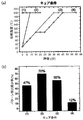
- summary of the pattern formation method of this invention The figure which shows the relationship between the heat processing (cure) temperature and the deformation
- the figure which shows the influence which imprint molding temperature conditions ((a) 100 degreeC, (b) 120 degreeC) have on pattern dimension stability.
- molding has on a pattern shrinkage rate.
- the present invention uses a solvent-soluble polyimide resin composition having photosensitivity and a glass transition temperature of 200 ° C. or lower in a polyimide submicrometer pattern forming method by a thermal imprint method, and after mold release, It is characterized by irradiating with ultraviolet rays before thermosetting.
- FIG. 1 is a diagram showing an outline of the thermal imprint method of the present invention.
- a polyimide film is applied to a substrate and then pre-baked ((a) film forming step). Then, after heating a polyimide film at the temperature below a glass transition temperature, the uneven
- the polyimide molded by the thermal imprint method is released from the mold, it is subjected to heat treatment (cure) in order to improve its heat resistance, light resistance and other properties.
- heat treatment cure
- film slippage reduction in polyimide film thickness
- pattern structure height deformation occur.
- (A) Film-forming process The solvent-soluble polyimide resin composition of the present invention is applied on a substrate such as Si (see FIG. 1 (a)).
- a substrate such as Si
- the coating method and the thickness of the coating film are not particularly limited, it is preferable to form a film of about 25 ⁇ m by a spin coating method.
- the coating film is dried by pre-baking.
- the solvent-soluble polyimide used in the present invention is imidized, it does not require high-temperature treatment necessary for imidization, can be molded at a low temperature below the glass transition temperature, and is solvent-soluble. It becomes a polyimide varnish, and film formation is possible only by skipping the solvent.
- Such a solvent-soluble polyimide is already known, and in the present invention, a commercially available one that can be molded at a glass transition temperature or lower can be appropriately selected and used. Among these, a block copolymer can be used. Thus, a solvent-soluble block copolymerized polyimide in which an arbitrary region giving desired properties is included in an arbitrary amount in the polyimide is preferably used.
- a solvent-soluble block copolymerized polyimide for example, a siloxane-modified block copolymerized polyimide having a low warpage characteristic using a diamine having a siloxane bond (siloxane bond-containing diamine) in a molecular skeleton as a diamine component (WO2002 / 023276, WO2005 / 116152).
- the block copolymerized polyimide can be molded at a glass transition temperature or lower, and is imidized polyimide, so that it can be molded at low temperature and with low shrinkage.
- Resin compositions using solvent-soluble polyimide are roughly classified into photosensitive and non-photosensitive. Since the imprint technique is a press technique using a mold, a pattern forming process by exposure is not required. Therefore, it is desirable to select non-photosensitivity in terms of process simplification. However, there is a problem of deformation of the pattern structure during heating for the heat treatment (curing).
- a highly accurate fine pattern forming method can be provided by using a photosensitive solvent-soluble polyimide resin composition.
- FIG. 2 shows a heat treatment in the case of using the photosensitive polyimide resin composition (a) used in Examples described later and the non-photosensitive polyimide resin composition (without the photosensitive agent) (b).
- (Cure) It is a figure which shows the relationship between temperature and a deformation
- the photosensitive solvent-soluble polyimide resin composition of the present invention contains the above-mentioned solvent-soluble polyimide, a photosensitizer, and a solvent, and the photosensitizer that imparts negative-type photosensitivity is used. It is done.
- the properties required as a mold material are releasability from polyimide, heat resistance and durability that can withstand the thermal imprint molding process, and Si, quartz, Ni, and some resins are used.
- flexible resin molds are easier to release due to large area molding than molds made of Si, quartz, Ni, etc., are capable of uniform pressure on non-flat surfaces, and are inexpensive. Suitable for uniform transfer over a large area.
- the main process parameters in this process are imprint temperature, imprint pressure, and imprint time, and the conditions vary depending on the object to be molded.
- the imprint temperature is preferably 40 ° C. or higher and not higher than the glass transition temperature of the polyimide resin composition to be used, more preferably 120 ° C.
- FIG. 3 is a diagram showing the influence of imprint molding temperature conditions ((a) 100 ° C., (b) 120 ° C.) on pattern dimensional stability.
- the thermal imprint molding temperature is one of the factors that can change the influence on the pattern shrinkage ratio after the heat treatment described later.
- the pattern shrinkage after curing could be reduced to 4% or less.
- the cooling method is not particularly limited, and natural cooling may be used, but from the viewpoint of the molding cycle, forced cooling such as flowing water through water pipes arranged around the molding space is preferable.
- Exposure depends on the photosensitizer used, but is usually performed by irradiating with ultraviolet rays.
- the reason for performing post-release exposure is that, when exposure was performed before release, there was a problem that the flexible resin mold and the polyimide film adhered after exposure.
- a transparent mold quartz, resin, etc.
- an opaque mold such as Si or Ni is also used. There is a merit that the selection range of is wide.
- the post-exposure baking (PEB) and the curing process can be integrated. it can.
- FIG. 4 is a diagram showing the influence of the heat treatment conditions after molding on the pattern shrinkage rate.
- the pattern shrinkage rate was examined under the following four types of heating conditions. (1) Heat for 20 minutes using a hot plate heated to 200 ° C. (2) Heat from room temperature to 200 ° C. at a heating rate of 20 ° C./min (3) Heat from room temperature to 200 ° C. at a heating rate of 5 ° C./min (4 ) Hold the photosensitive polyimide resin composition used at a post-exposure bake temperature (100 ° C) for a certain period of time and heat from room temperature to 200 ° C at a heating rate of 5 ° C / min.
- the range of change in shrinkage due to change in heat treatment conditions after molding is 70 to 12%.
- two-stage heating at a heating rate of 5 ° C./min, that is, during the heating, is maintained at 100 ° C., which is the post-exposure baking temperature of the used photosensitive polyimide resin composition, and then reheated.
- the shrinkage rate could be improved to 14% or less.
- Example 1 Formation of micrometer pattern
- a commercially available organic solvent-soluble polyimide resin composition (Q-RP-X1149-X, PI R & D Co., Ltd) was used.
- the composition contains a solvent-soluble siloxane-modified block copolymerized polyimide (glass transition temperature 192 ° C.), gamma butyrolactone (solvent), methyl benzoate (solvent), and a photosensitizing agent, and a cured film
- a solvent-soluble siloxane-modified block copolymerized polyimide glass transition temperature 192 ° C.
- gamma butyrolactone gamma butyrolactone
- methyl benzoate methyl benzoate
- photosensitizing agent a photosensitizing agent
- a Si substrate (thickness: 725 ⁇ m, diameter: 8 inches) was used as the base material.
- the mold uses a commercially available resin sheet (Obducat AB, intermediate polymer stamp (IPS) sheet, glass transition temperature: 150 ° C., manufactured by Obducat AB) because it has hydrophobic properties, and is heated in as follows. It was produced by a printing process.
- Obducat AB intermediate polymer stamp (IPS) sheet, glass transition temperature: 150 ° C., manufactured by Obducat AB
- the resin film having a film thickness of 200 ⁇ m was softened by heating it to near the glass transition temperature, and pressure-molded for 2 minutes at an imprint pressure of 4 MPa using an Si master mold. Then, it cooled to 60 degreeC and released from the mold.
- the resin composition was spin-coated on the substrate made of Si to a film thickness of 25 ⁇ m and then pre-baked at 100 ° C. for 4 minutes to form a resin film.
- the resin film was softened by heating to 100 to 120 ° C. in a state where the mold was placed on the substrate having the resin film, followed by pressure molding. Then, it cooled to 60 degreeC and released from the mold.
- the surface of the molded resin film was irradiated with ultraviolet rays (wavelength: 365 nm, illuminance: 30 mW / cm 2 ) using an ultraviolet photogen installed in the nanoimprint apparatus, and then heated at a heating rate of 5 ° C./min. After heating to 100 ° C. and holding at 100 ° C., a heat treatment by two-stage heating was performed in which heating was further performed to 200 ° C.
- the illuminance of ultraviolet irradiation, the exposure time, and the exposure dose were 30 mW / cm 2 , 40 seconds, and 1200 mJ / cm 2 , respectively.
- FIG. 5 shows a photograph showing the L & S of the imprint pattern produced in this example.
- an L & S pattern structure of 50 ⁇ m to 3 ⁇ m having a clean line edge and a rectangular cross section is well formed.
- Example 2 Formation of sub-micrometer pattern
- a Si substrate having a thickness of 500 ⁇ m and a diameter of 4 inches was used, and the depth of 188 nm, the line widths of 150 nm, 200 nm, and 300 nm were the same as in Example 1 except that the pressing time was 3 minutes.
- a mold having three types of uneven patterns was used.
- a submicrometer pattern was formed in the same manner as in Example 1 except for the substrate and the mold.
- FIG. 6 shows a photograph showing the L & S of the imprint pattern produced according to this example.
- a submicrometer pattern structure having a rectangular cross section is well formed.
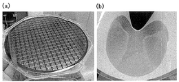
- the molded polyimide can be physically peeled off by performing water-repellent treatment etc. on the underlying Si substrate in advance, regardless of before or after curing, flexible polyimide substrate Can also be produced.
- FIG. 7 is a photograph of the flexible polyimide substrate obtained in the example, where (a) is after thermal imprint molding, and (b) is after peeling from the Si substrate (before curing).
Landscapes
- Physics & Mathematics (AREA)
- General Physics & Mathematics (AREA)
- Chemical & Material Sciences (AREA)
- Health & Medical Sciences (AREA)
- Organic Chemistry (AREA)
- Chemical Kinetics & Catalysis (AREA)
- Medicinal Chemistry (AREA)
- Polymers & Plastics (AREA)
- Spectroscopy & Molecular Physics (AREA)
- Mechanical Engineering (AREA)
- Engineering & Computer Science (AREA)
- Toxicology (AREA)
- Oral & Maxillofacial Surgery (AREA)
- Thermal Sciences (AREA)
- Electromagnetism (AREA)
- Exposure Of Semiconductors, Excluding Electron Or Ion Beam Exposure (AREA)
- Shaping Of Tube Ends By Bending Or Straightening (AREA)
- Moulds For Moulding Plastics Or The Like (AREA)
- Materials For Photolithography (AREA)
Abstract
Description
感光性を有する、ガラス転移温度以下での成形が可能な溶剤可溶性ポリイミド樹脂組成物を用いるとともに、モールド離型後であって、熱硬化の前に、紫外線を照射することを特徴とするポリイミドの微細パターン形成方法。
Siなどの基板上に、本発明の溶剤可溶性ポリイミド樹脂組成物を塗布する(図1(a)参照)。塗布法及び塗布膜の厚さは、特に限定されないが、回転塗布法により25μm程度の膜を形成することが好ましい。
その後、凹凸が形成されたモールドを用いた熱インプリント成形によるパターン形成(転写)を行う(図1(b)参照)。すなわち、前工程で得られたポリイミド膜を有する基板を所定温度に加熱した後、凹凸パターンが形成されたモールドを用いて加圧成形する。
インプリント成形後には、ポリイミドとモールドをガラス転移温度以下より低い温度、例えば、60℃まで冷却し、離型する(図1(c)参照)。
離型した後、露光を行う(図1(d)参照)。
最終工程は、熱処理である(図1(e))。
(1)200℃に加熱したホットプレートを用いて20分間加熱
(2)加熱速度20℃/分で室温から200℃まで加熱
(3)加熱速度5℃/分で室温から200℃まで加熱
(4)用いた感光性ポリイミド樹脂組成物のポストエクスポージャーベーク温度(100℃)で一定時間保持して、加熱速度5℃/分で室温から200℃まで加熱
本実施例では、市販の有機溶剤可溶性ポリイミド樹脂組成物(Q-RP-X1149-X,PI R&D Co.,Ltd)を用いた。
本実施例においては、厚み500μm、直径4インチのSi基板を用い、加圧時間を3分としたこと以外は実施例1と同様にして、深さ188nm、線幅150nm,200nm,及び300nmの3種の凹凸パターンを作製したモールドを用いた。
Claims (5)
- 熱インプリント法によるポリイミドの微細パターン形成方法において、
感光性を有する、ガラス転移温度以下での成形が可能な溶剤可溶性ポリイミド樹脂組成物を用いるとともに、モールド離型後であって、熱硬化の前に、紫外線を照射することを特徴とするポリイミドの微細パターン形成方法。 - 前記熱硬化を、室温から熱処理温度まで昇温させる途中で前記の溶剤可溶性ポリイミド樹脂組成物のポストエクスポージャーベーク温度に一定時間保持する2段加熱により行うことを特徴とする請求項1に記載の、ポリイミドの微細パターン形成方法。
- 前記微細パターンが、矩形断面を有するサブマイクロメートルパターンであることを特徴とする請求項1又は2に記載の、ポリイミドの微細パターン形成方法。
- 前記溶剤可溶性ポリイミドが、ブロック共重合ポリイミドであることを特徴とする請求項1~3のいずれか一項に記載の、ポリイミドの微細パターン形成方法。
- 請求項1~4のいずれか一項に記載の微細パターン形成方法で製造された、矩形断面を有するサブマイクロメートルパターンが形成されたポリイミド。
Priority Applications (4)
| Application Number | Priority Date | Filing Date | Title |
|---|---|---|---|
| CN201480056987.7A CN105658413B (zh) | 2013-10-18 | 2014-08-29 | 利用压印法的聚酰亚胺的精细图案形成方法 |
| JP2015542536A JP6192023B2 (ja) | 2013-10-18 | 2014-08-29 | インプリント法によるポリイミドの微細パターン形成方法 |
| US15/029,481 US10189203B2 (en) | 2013-10-18 | 2014-08-29 | Method for forming micropattern of polyimide using imprinting |
| KR1020167008515A KR101770809B1 (ko) | 2013-10-18 | 2014-08-29 | 임프린트법에 의한 폴리이미드의 미세 패턴 형성 방법 |
Applications Claiming Priority (2)
| Application Number | Priority Date | Filing Date | Title |
|---|---|---|---|
| JP2013217645 | 2013-10-18 | ||
| JP2013-217645 | 2013-10-18 |
Publications (1)
| Publication Number | Publication Date |
|---|---|
| WO2015056487A1 true WO2015056487A1 (ja) | 2015-04-23 |
Family
ID=52827940
Family Applications (1)
| Application Number | Title | Priority Date | Filing Date |
|---|---|---|---|
| PCT/JP2014/072804 Ceased WO2015056487A1 (ja) | 2013-10-18 | 2014-08-29 | インプリント法によるポリイミドの微細パターン形成方法 |
Country Status (6)
| Country | Link |
|---|---|
| US (1) | US10189203B2 (ja) |
| JP (1) | JP6192023B2 (ja) |
| KR (1) | KR101770809B1 (ja) |
| CN (1) | CN105658413B (ja) |
| TW (1) | TWI659819B (ja) |
| WO (1) | WO2015056487A1 (ja) |
Cited By (7)
| Publication number | Priority date | Publication date | Assignee | Title |
|---|---|---|---|---|
| JP2017034166A (ja) * | 2015-08-04 | 2017-02-09 | 株式会社東芝 | 基板処理方法 |
| JP2017103384A (ja) * | 2015-12-03 | 2017-06-08 | 大日本印刷株式会社 | インプリントモールド及びその製造方法、並びにインプリント方法 |
| JP2019054016A (ja) * | 2017-09-12 | 2019-04-04 | 東芝メモリ株式会社 | テンプレート、テンプレートの作製方法、および半導体装置の製造方法 |
| JP2019517974A (ja) * | 2016-03-17 | 2019-06-27 | コーニング インコーポレイテッド | 曲げられる電子デバイスモジュールおよび物品、並びにそれを製造するための結合方法 |
| WO2020112740A1 (en) * | 2018-11-29 | 2020-06-04 | Sharklet Technologies, Inc. | Soluble templates and methods of manufacture thereof |
| JP2022508102A (ja) * | 2018-11-15 | 2022-01-19 | アプライド マテリアルズ インコーポレイテッド | マイクロインプリントによるビア形成の方法 |
| JP2023069726A (ja) * | 2021-11-08 | 2023-05-18 | 綜研化学株式会社 | ポリイミドの微細パターン形成方法 |
Families Citing this family (3)
| Publication number | Priority date | Publication date | Assignee | Title |
|---|---|---|---|---|
| CN109817827B (zh) * | 2019-01-22 | 2021-01-01 | 深圳市华星光电半导体显示技术有限公司 | Oled显示面板的制作设备及制作方法 |
| US10727083B1 (en) * | 2019-02-25 | 2020-07-28 | Applied Materials, Inc. | Method for via formation in flowable epoxy materials by micro-imprint |
| CN110619818B (zh) * | 2019-08-27 | 2021-04-27 | 武汉华星光电半导体显示技术有限公司 | 一种显示面板及其制作方法 |
Citations (6)
| Publication number | Priority date | Publication date | Assignee | Title |
|---|---|---|---|---|
| JP2003183496A (ja) * | 2001-12-13 | 2003-07-03 | Toray Ind Inc | ポリイミド前駆体組成物 |
| JP2008307808A (ja) * | 2007-06-15 | 2008-12-25 | Hitachi Metals Ltd | 凹凸付金属基板の製造方法 |
| JP2010260902A (ja) * | 2009-04-30 | 2010-11-18 | Pi R & D Co Ltd | 感光性変性ポリイミド樹脂組成物及びその用途 |
| JP2011077251A (ja) * | 2009-09-30 | 2011-04-14 | Toray Ind Inc | ディスプレイ用部材および製造方法 |
| JP2013042124A (ja) * | 2011-07-19 | 2013-02-28 | Tokuyama Corp | 光硬化性ナノインプリント用組成物を用いたパターンの製造方法 |
| JP2013154637A (ja) * | 2012-01-06 | 2013-08-15 | Nippon Shokubai Co Ltd | 樹脂製ナノ構造体の製造方法 |
Family Cites Families (12)
| Publication number | Priority date | Publication date | Assignee | Title |
|---|---|---|---|---|
| US7648815B2 (en) | 2000-09-12 | 2010-01-19 | Pi R&D Co., Ltd. | Negative photosensitive polyimide composition and method for forming image the same |
| JP2003234283A (ja) * | 2002-02-08 | 2003-08-22 | Asahi Kasei Corp | パターン形成方法 |
| CN1229420C (zh) | 2002-03-29 | 2005-11-30 | 中国科学院化学研究所 | 一种本征型光敏性聚酰亚胺树脂及其制备方法和用途 |
| US7037637B2 (en) | 2002-07-17 | 2006-05-02 | Nitto Denko Corporation | Photosensitive polyimide resin precursor composition, optical polyimide obtained from the composition, optical waveguide using the polyimide, and process for producing the optical waveguide |
| JP3947457B2 (ja) | 2002-11-29 | 2007-07-18 | 日東電工株式会社 | ポリイミド光導波路の製造方法 |
| JPWO2005116152A1 (ja) | 2004-05-27 | 2008-04-03 | 株式会社ピーアイ技術研究所 | 印刷用ブロック共重合ポリイミドインク組成物 |
| CN1978529A (zh) * | 2005-12-06 | 2007-06-13 | 北京波米科技有限公司 | 光敏性聚酰亚胺树脂和组合物与制备方法 |
| WO2007100078A1 (ja) | 2006-03-03 | 2007-09-07 | Pi R & D Co., Ltd. | スクリーン印刷用感光性インク組成物及びそれを用いたポジ型レリーフパターンの形成方法 |
| US20100258163A1 (en) * | 2009-04-14 | 2010-10-14 | Honeywell International Inc. | Thin-film photovoltaics |
| JP5272924B2 (ja) * | 2009-06-29 | 2013-08-28 | 日立化成株式会社 | 光重合性モノマー組成物並びに微細構造加工体及びその製造方法 |
| JP2011206938A (ja) * | 2010-03-29 | 2011-10-20 | Kanagawa Acad Of Sci & Technol | 熱インプリント用モールドおよびその製造方法並びにそのモールドを用いた樹脂材の製造方法 |
| JP6379458B2 (ja) * | 2012-09-13 | 2018-08-29 | 日立化成株式会社 | パターンを有する樹脂層を製造する方法、及びそれに用いられる樹脂組成物 |
-
2014
- 2014-08-29 KR KR1020167008515A patent/KR101770809B1/ko active Active
- 2014-08-29 US US15/029,481 patent/US10189203B2/en active Active
- 2014-08-29 WO PCT/JP2014/072804 patent/WO2015056487A1/ja not_active Ceased
- 2014-08-29 CN CN201480056987.7A patent/CN105658413B/zh active Active
- 2014-08-29 JP JP2015542536A patent/JP6192023B2/ja active Active
- 2014-10-01 TW TW103134289A patent/TWI659819B/zh not_active IP Right Cessation
Patent Citations (6)
| Publication number | Priority date | Publication date | Assignee | Title |
|---|---|---|---|---|
| JP2003183496A (ja) * | 2001-12-13 | 2003-07-03 | Toray Ind Inc | ポリイミド前駆体組成物 |
| JP2008307808A (ja) * | 2007-06-15 | 2008-12-25 | Hitachi Metals Ltd | 凹凸付金属基板の製造方法 |
| JP2010260902A (ja) * | 2009-04-30 | 2010-11-18 | Pi R & D Co Ltd | 感光性変性ポリイミド樹脂組成物及びその用途 |
| JP2011077251A (ja) * | 2009-09-30 | 2011-04-14 | Toray Ind Inc | ディスプレイ用部材および製造方法 |
| JP2013042124A (ja) * | 2011-07-19 | 2013-02-28 | Tokuyama Corp | 光硬化性ナノインプリント用組成物を用いたパターンの製造方法 |
| JP2013154637A (ja) * | 2012-01-06 | 2013-08-15 | Nippon Shokubai Co Ltd | 樹脂製ナノ構造体の製造方法 |
Cited By (11)
| Publication number | Priority date | Publication date | Assignee | Title |
|---|---|---|---|---|
| JP2017034166A (ja) * | 2015-08-04 | 2017-02-09 | 株式会社東芝 | 基板処理方法 |
| US10249545B2 (en) | 2015-08-04 | 2019-04-02 | Toshiba Memory Corporation | Method for processing substrate including forming a film on a silicon-containing surface of the substrate to prevent resist from extruding from the substrate during an imprinting process |
| JP2017103384A (ja) * | 2015-12-03 | 2017-06-08 | 大日本印刷株式会社 | インプリントモールド及びその製造方法、並びにインプリント方法 |
| JP2019517974A (ja) * | 2016-03-17 | 2019-06-27 | コーニング インコーポレイテッド | 曲げられる電子デバイスモジュールおよび物品、並びにそれを製造するための結合方法 |
| US11104601B2 (en) | 2016-03-17 | 2021-08-31 | Corning Incorporated | Bendable electronic device modules, articles and bonding methods of making the same |
| JP2019054016A (ja) * | 2017-09-12 | 2019-04-04 | 東芝メモリ株式会社 | テンプレート、テンプレートの作製方法、および半導体装置の製造方法 |
| JP2022508102A (ja) * | 2018-11-15 | 2022-01-19 | アプライド マテリアルズ インコーポレイテッド | マイクロインプリントによるビア形成の方法 |
| JP7515474B2 (ja) | 2018-11-15 | 2024-07-12 | アプライド マテリアルズ インコーポレイテッド | マイクロインプリントによるビア形成の方法 |
| WO2020112740A1 (en) * | 2018-11-29 | 2020-06-04 | Sharklet Technologies, Inc. | Soluble templates and methods of manufacture thereof |
| CN113365795A (zh) * | 2018-11-29 | 2021-09-07 | 善洁科技有限公司 | 可溶性模板和其制造方法 |
| JP2023069726A (ja) * | 2021-11-08 | 2023-05-18 | 綜研化学株式会社 | ポリイミドの微細パターン形成方法 |
Also Published As
| Publication number | Publication date |
|---|---|
| CN105658413A (zh) | 2016-06-08 |
| CN105658413B (zh) | 2018-03-16 |
| US20160263814A1 (en) | 2016-09-15 |
| JPWO2015056487A1 (ja) | 2017-03-09 |
| KR20160048975A (ko) | 2016-05-04 |
| TW201524747A (zh) | 2015-07-01 |
| US10189203B2 (en) | 2019-01-29 |
| KR101770809B1 (ko) | 2017-08-23 |
| JP6192023B2 (ja) | 2017-09-06 |
| TWI659819B (zh) | 2019-05-21 |
Similar Documents
| Publication | Publication Date | Title |
|---|---|---|
| JP6192023B2 (ja) | インプリント法によるポリイミドの微細パターン形成方法 | |
| CN101923282B (zh) | 纳米压印抗蚀剂及采用该纳米压印抗蚀剂的纳米压印方法 | |
| CN101923279B (zh) | 纳米压印模板及其制备方法 | |
| TWI500638B (zh) | 奈米壓印用硬化性組成物及硬化物 | |
| JP5308287B2 (ja) | ナノインプリントを用いたパターン成形方法とパターン成形のためのモールド製作方法 | |
| JP3819397B2 (ja) | インプリント方法 | |
| KR101416625B1 (ko) | 미세 패턴 형성용 고분자 몰드의 제조 방법, 이에 의해 제조되는 미세 패턴 형성용 고분자 몰드, 및 이를 이용한 미세 패턴 형성 방법 | |
| JP2008296579A (ja) | マスクモールド及びその製作方法と、製作されたマスクモールドを用いた大面積・微細パターン成形方法 | |
| CN101738860B (zh) | 用于压印工艺的光敏树脂组合物以及用于在基板之上形成有机层的方法 | |
| KR20080000297A (ko) | 광경화 타입 소수성 몰드 및 그 제조방법 | |
| CN113484945A (zh) | 一种基于pdms/pua相互复制的可变线密度光栅制作方法 | |
| JP2014096593A (ja) | マイクロコンタクトプリンティング用スタンプ作製用マスター版の製造方法、マイクロコンタクトプリンティング用スタンプ作製用マスター版、およびマイクロコンタクトプリンティング用スタンプの製造方法。 | |
| CN101165591B (zh) | 软平板印刷技术制作二维聚合物光子晶体的方法 | |
| CN108109952B (zh) | 微拾取阵列及其制造方法 | |
| CN102799066A (zh) | 一种在二氧化钛有机无机光敏复合薄膜上制备凹透镜阵列结构的方法 | |
| JP2008078550A (ja) | インプリントモールドおよびその製造方法およびパターン形成方法 | |
| CN110441838A (zh) | 基于二氧化钛有机-无机光敏复合薄膜异形凸透镜阵列的制备方法 | |
| Youn et al. | Microstructuring of SU-8 photoresist by UV-assisted thermal imprinting with non-transparent mold | |
| JP6491928B2 (ja) | レプリカモールドおよびその製造方法 | |
| CN101923283A (zh) | 纳米压印抗蚀剂及采用该纳米压印抗蚀剂的纳米压印方法 | |
| TWI423307B (zh) | 製造微結構的方法 | |
| US12346024B2 (en) | Method of manufacturing a master for a replication process | |
| TWI389931B (zh) | 奈米壓印抗蝕劑及採用該奈米壓印抗蝕劑的奈米壓印方法 | |
| WO2020080372A1 (ja) | 微細パターン成形方法、インプリント用モールド製造方法およびインプリント用モールド並びに光学デバイス | |
| KR20080098212A (ko) | 포토리소그래피와 나노임프린트 리소그래피를 결합한리소그래피 방법 |
Legal Events
| Date | Code | Title | Description |
|---|---|---|---|
| 121 | Ep: the epo has been informed by wipo that ep was designated in this application |
Ref document number: 14853597 Country of ref document: EP Kind code of ref document: A1 |
|
| ENP | Entry into the national phase |
Ref document number: 2015542536 Country of ref document: JP Kind code of ref document: A |
|
| ENP | Entry into the national phase |
Ref document number: 20167008515 Country of ref document: KR Kind code of ref document: A |
|
| WWE | Wipo information: entry into national phase |
Ref document number: 15029481 Country of ref document: US |
|
| NENP | Non-entry into the national phase |
Ref country code: DE |
|
| 122 | Ep: pct application non-entry in european phase |
Ref document number: 14853597 Country of ref document: EP Kind code of ref document: A1 |