WO2015053022A1 - 半導体装置 - Google Patents
半導体装置 Download PDFInfo
- Publication number
- WO2015053022A1 WO2015053022A1 PCT/JP2014/073578 JP2014073578W WO2015053022A1 WO 2015053022 A1 WO2015053022 A1 WO 2015053022A1 JP 2014073578 W JP2014073578 W JP 2014073578W WO 2015053022 A1 WO2015053022 A1 WO 2015053022A1
- Authority
- WO
- WIPO (PCT)
- Prior art keywords
- region
- diffusion region
- potential
- semiconductor
- semiconductor region
- Prior art date
- Legal status (The legal status is an assumption and is not a legal conclusion. Google has not performed a legal analysis and makes no representation as to the accuracy of the status listed.)
- Ceased
Links
Images





Classifications
-
- H—ELECTRICITY
- H10—SEMICONDUCTOR DEVICES; ELECTRIC SOLID-STATE DEVICES NOT OTHERWISE PROVIDED FOR
- H10D—INORGANIC ELECTRIC SEMICONDUCTOR DEVICES
- H10D89/00—Aspects of integrated devices not covered by groups H10D84/00 - H10D88/00
- H10D89/60—Integrated devices comprising arrangements for electrical or thermal protection, e.g. protection circuits against electrostatic discharge [ESD]
- H10D89/601—Integrated devices comprising arrangements for electrical or thermal protection, e.g. protection circuits against electrostatic discharge [ESD] for devices having insulated gate electrodes, e.g. for IGFETs or IGBTs
- H10D89/811—Integrated devices comprising arrangements for electrical or thermal protection, e.g. protection circuits against electrostatic discharge [ESD] for devices having insulated gate electrodes, e.g. for IGFETs or IGBTs using FETs as protective elements
- H10D89/819—Bias arrangements for gate electrodes of FETs, e.g. RC networks or voltage partitioning circuits
-
- H—ELECTRICITY
- H10—SEMICONDUCTOR DEVICES; ELECTRIC SOLID-STATE DEVICES NOT OTHERWISE PROVIDED FOR
- H10D—INORGANIC ELECTRIC SEMICONDUCTOR DEVICES
- H10D62/00—Semiconductor bodies, or regions thereof, of devices having potential barriers
- H10D62/10—Shapes, relative sizes or dispositions of the regions of the semiconductor bodies; Shapes of the semiconductor bodies
- H10D62/113—Isolations within a component, i.e. internal isolations
-
- H—ELECTRICITY
- H10—SEMICONDUCTOR DEVICES; ELECTRIC SOLID-STATE DEVICES NOT OTHERWISE PROVIDED FOR
- H10D—INORGANIC ELECTRIC SEMICONDUCTOR DEVICES
- H10D84/00—Integrated devices formed in or on semiconductor substrates that comprise only semiconducting layers, e.g. on Si wafers or on GaAs-on-Si wafers
- H10D84/80—Integrated devices formed in or on semiconductor substrates that comprise only semiconducting layers, e.g. on Si wafers or on GaAs-on-Si wafers characterised by the integration of at least one component covered by groups H10D12/00 or H10D30/00, e.g. integration of IGFETs
- H10D84/82—Integrated devices formed in or on semiconductor substrates that comprise only semiconducting layers, e.g. on Si wafers or on GaAs-on-Si wafers characterised by the integration of at least one component covered by groups H10D12/00 or H10D30/00, e.g. integration of IGFETs of only field-effect components
- H10D84/83—Integrated devices formed in or on semiconductor substrates that comprise only semiconducting layers, e.g. on Si wafers or on GaAs-on-Si wafers characterised by the integration of at least one component covered by groups H10D12/00 or H10D30/00, e.g. integration of IGFETs of only field-effect components of only insulated-gate FETs [IGFET]
- H10D84/85—Complementary IGFETs, e.g. CMOS
-
- H—ELECTRICITY
- H10—SEMICONDUCTOR DEVICES; ELECTRIC SOLID-STATE DEVICES NOT OTHERWISE PROVIDED FOR
- H10D—INORGANIC ELECTRIC SEMICONDUCTOR DEVICES
- H10D84/00—Integrated devices formed in or on semiconductor substrates that comprise only semiconducting layers, e.g. on Si wafers or on GaAs-on-Si wafers
- H10D84/80—Integrated devices formed in or on semiconductor substrates that comprise only semiconducting layers, e.g. on Si wafers or on GaAs-on-Si wafers characterised by the integration of at least one component covered by groups H10D12/00 or H10D30/00, e.g. integration of IGFETs
- H10D84/82—Integrated devices formed in or on semiconductor substrates that comprise only semiconducting layers, e.g. on Si wafers or on GaAs-on-Si wafers characterised by the integration of at least one component covered by groups H10D12/00 or H10D30/00, e.g. integration of IGFETs of only field-effect components
- H10D84/83—Integrated devices formed in or on semiconductor substrates that comprise only semiconducting layers, e.g. on Si wafers or on GaAs-on-Si wafers characterised by the integration of at least one component covered by groups H10D12/00 or H10D30/00, e.g. integration of IGFETs of only field-effect components of only insulated-gate FETs [IGFET]
- H10D84/85—Complementary IGFETs, e.g. CMOS
- H10D84/859—Complementary IGFETs, e.g. CMOS comprising both N-type and P-type wells, e.g. twin-tub
-
- H—ELECTRICITY
- H10—SEMICONDUCTOR DEVICES; ELECTRIC SOLID-STATE DEVICES NOT OTHERWISE PROVIDED FOR
- H10W—GENERIC PACKAGES, INTERCONNECTIONS, CONNECTORS OR OTHER CONSTRUCTIONAL DETAILS OF DEVICES COVERED BY CLASS H10
- H10W10/00—Isolation regions in semiconductor bodies between components of integrated devices
- H10W10/01—Manufacture or treatment
- H10W10/031—Manufacture or treatment of isolation regions comprising PN junctions
-
- H—ELECTRICITY
- H10—SEMICONDUCTOR DEVICES; ELECTRIC SOLID-STATE DEVICES NOT OTHERWISE PROVIDED FOR
- H10W—GENERIC PACKAGES, INTERCONNECTIONS, CONNECTORS OR OTHER CONSTRUCTIONAL DETAILS OF DEVICES COVERED BY CLASS H10
- H10W10/00—Isolation regions in semiconductor bodies between components of integrated devices
- H10W10/30—Isolation regions comprising PN junctions
Definitions
- the present invention relates to a semiconductor device.
- HVICs high-voltage ICs
- Non-Patent Document 1 discloses a high voltage IC manufactured (manufactured) by this self-separating IC process. The structure of a high voltage IC manufactured by a self-separating IC process will be described.
- FIG. 9 is a plan view schematically showing a planar structure of a conventional high voltage IC.
- FIG. 10 is a cross-sectional view showing a cross-sectional structure taken along section line AA-AA ′ of FIG.
- FIG. 11 is a circuit diagram showing an equivalent circuit of the high voltage IC of FIG.
- the high voltage IC 200 generally includes a high side drive circuit 210, a level shifter 214, and a control circuit 215.
- the high side drive circuit 210 includes a gate drive circuit, a level shift resistor, and the like.
- the high side drive circuit 210 is disposed in the high side region 220.
- the periphery of the high side region 220 is surrounded by a high breakdown voltage isolation region 224.
- the high side region 220 is electrically isolated from the low side region 225 by the high breakdown voltage isolation region 224.
- the level shifter 214 is disposed in the high breakdown voltage isolation region 224.
- a level shift resistor 217 is connected between the VB terminal and the level shifter 214.
- the periphery of the high breakdown voltage isolation region 224 is surrounded by the low side region 225.
- a control circuit 215 that controls the high-side drive circuit 210 is disposed in the low-side region 225.
- the low side region 225 is a portion excluding the high side region 220, the high breakdown voltage isolation region 224, and the level shifter 214.
- the gate drive circuit constituting the high-side drive circuit 210 includes a high-side p-channel MOSFET (insulated gate field effect transistor, hereinafter referred to as PMOS) 212 and an n-channel MOSFET (hereinafter referred to as NMOS) 213. It consists of CMOS (complementary MOS) circuits connected in a complementary manner.
- CMOS complementary MOS
- a lateral PMOS 212 of the high side drive circuit 210 is formed in an n diffusion region 202 selectively provided in the surface layer of the p ⁇ bulk substrate 201.
- a p-type diffusion region 203 is provided in the n-type diffusion region 202 with a relatively shallow depth, and a lateral NMOS 213 is formed in the p-type diffusion region 203.
- the n diffusion region 202 is connected to the VB terminal that is the highest potential of the high side drive circuit 210.
- the p diffusion region 203 is connected to the VS terminal that is the lowest potential of the high side drive circuit 210.
- the potential difference between the VB terminal and the VS terminal is, for example, about 15 V, which is the power supply voltage of the high side drive circuit 210.
- n diffusion region 202 on the outside of the n diffusion region 202, p in the low side region 225 - region 204 are provided.
- the p ⁇ bulk substrate 201 and the p ⁇ region 204 are connected to the GND terminal of the ground potential (for example, 0 V).
- an n ⁇ low concentration diffusion region 205 constituting the high breakdown voltage isolation region 224 is provided between the n diffusion region 202 and the p ⁇ region 204.
- the pn junction between the n ⁇ low concentration diffusion region 205 and the p ⁇ region 204 is reverse-biased, thereby causing the n ⁇
- the low-concentration diffusion region 205 is depleted, and the breakdown voltage in the lateral direction (direction parallel to the main surface of the substrate) is maintained.
- the high voltage IC 200 is connected to, for example, a power conversion bridge circuit, and drives the first and second MOSFETs 101 and 102 constituting one phase of the power conversion bridge circuit.
- the first and second MOSFETs 101 and 102 are connected in series between a high-voltage main power supply (positive electrode side) Vdc and a ground potential GND on the negative electrode side of the main power supply.
- the VS terminal is connected to a connection point 105 between the first MOSFET 101 and the second MOSFET 102.
- a connection point 105 is an output point of the bridge circuit configured by the first and second MOSFETs 101 and 102.
- Reference numerals 103 and 104 denote FWDs (reflux diodes).
- the operation of the high voltage IC 200 will be described by taking as an example the case of driving the first MOSFET 101 on the high side of the power conversion bridge circuit.
- the high side drive circuit 210 operates at a potential between the reference potential VS and the power supply potential VB which is the highest potential of the high side drive circuit 210, with the potential at the connection point 105 connected to the VS terminal as the reference potential VS. .
- the power supply potential VB of the high side drive circuit 210 is higher than the reference potential VS by the voltage of the bootstrap capacitor.
- the control circuit 215 operates with the ground potential GND as a reference, and generates a GND-based on / off control signal for turning on / off the first MOSFET 101.
- the GND-based on / off control signal is converted into a VS-based on / off control signal by the level shifter 214 and transmitted to the high-side drive circuit 210.
- the on / off signal input to the high side driving circuit 210 is input to the gate of the first MOSFET 101 via the gate driving circuit 211.
- the first MOSFET 101 is turned on / off based on the on / off signal. As described above, the first MOSFET 101 is turned on / off based on the on / off signal from the control circuit 215 transmitted through the level shifter 214, and combined with the on / off of the second MOSFET 102, thereby the potential of the VS terminal. Varies between 0 V (GND) and several hundred V (Vdc).
- the high breakdown voltage isolation region between the level shift n-channel MOSFET and the isolation island region is made of a p-type substrate instead of the conventional p diffusion region and the surrounding RESURF region.
- a device that achieves downsizing without increasing the manufacturing cost by making the p-type substrate region (or the p diffusion layer) a region exposed on the front surface of the substrate for example, the following patent document). 1.
- Patent Document 1 a potential difference between n diffusion regions divided by a high breakdown voltage isolation region is used as a signal voltage at the time of level shift.
- one n diffusion region (isolation island region) divided by the high breakdown voltage isolation region is set as a power supply potential
- the other n diffusion region is set as the drain potential of the level shift n-channel MOSFET.
- the drain potential of the level shift n-channel MOSFET becomes the power supply potential of the high voltage IC when the level shift n-channel MOSFET is in the off state, and the level shift resistor and the level shift when the level shift n-channel MOSFET is in the on state.
- the potential is lower than the power supply potential by a voltage value obtained by multiplying the current value of the n-channel MOSFET for use.
- the following devices have been proposed as conventional high voltage ICs.
- p - -type silicon substrate, p - n surrounded by well regions - apart and region, and a drain n + region connected to the drain electrode, and the drain n + region, p base region surrounding the drain n + region And a source n + region disposed inside the p base region.
- n - region, n - through the space p - than the region, the 1n - - p to reach the -type silicon substrate is separated into a region - region and the 2n.
- a drain n + region is provided in the first n ⁇ region.
- the first n ⁇ region has a floating potential (see, for example, Patent Document 2 below).
- the p + diffusion region of the PMOS 212 is used as the emitter
- the n diffusion region 202 is used as the base
- the p ⁇ bulk substrate 201 is used as the collector in the high side region 220.
- a parasitic pnp bipolar transistor 218 having the p diffusion region 203 as an emitter, the n diffusion region 202 as a base, and a p ⁇ bulk substrate 201 as a collector.
- the p + diffusion region of the PMOS212 the emitter, the n diffusion region 202 as a base, p - parasitic pnp bipolar transistor bulk substrate 201 and the collector because the depth of the n diffusion region 202 serving as the base is deep, hFE ( (DC current amplification factor) is small and thermal runaway is difficult.
- the depth of the p diffusion region 203 serving as the emitter is deeper than the depth of the p + diffusion region of the PMOS 212, and the base width (the p diffusion region 203 and the p ⁇ of the n diffusion region 202). - the thickness of the part sandwiched between the bulk substrate 201) is narrow, and the emitter of the p + diffusion region of the PMOS212, the n diffusion region 202 as a base, p - parasitic pnp bipolar transistor to the collector of the bulk substrate 201 HFE is larger than that, and it is easy to run away.
- the base, emitter, and collector of the parasitic pnp bipolar transistor 218 having a narrow base width are connected to the VB terminal, the VS terminal, and the GND terminal, respectively.
- the power supply potential VB of the high voltage IC 200 is higher than the reference potential VS, so that the parasitic pnp bipolar transistor 218 does not operate.
- the power supply potential VB is lowered by 0.6 V or more, which is the diffusion potential of the silicon pn junction, from the reference potential VS due to the negative voltage surge, that is, the potential relationship is VB ⁇ (VS ⁇ 0.6 [V]).
- the pn junction between the p diffusion region 203 (emitter) and the n diffusion region 202 (base) is forward biased, and the parasitic pnp bipolar transistor 218 having a narrow base width is turned on. Accordingly, there is a problem that a large current flows between the VS terminal to which a high voltage (up to Vdc on the high potential side) is applied and the GND terminal, and the high voltage IC 200 is destroyed due to heat generated by the large current.
- bypass capacitor connected as an external component is disposed outside the substrate 201.
- the bypass capacitor cannot be connected due to layout design and cost restrictions, or cannot be placed near the high voltage IC 200 due to layout design restrictions, and is placed at a position away from the high voltage IC 200. There is a problem that the effect cannot be obtained sufficiently.
- An object of the present invention is to provide a semiconductor device that can prevent a breakdown due to a surge in order to solve the problems caused by the above-described conventional technology.
- a semiconductor device is connected to a first potential selectively provided on a surface layer of a semiconductor layer of a first conductivity type.
- a first semiconductor region of two conductivity type and a second semiconductor region of second conductivity type that is selectively provided on the surface layer of the semiconductor layer and is connected to a second potential or floating potential lower than the first potential
- a third semiconductor region of a first conductivity type that is selectively provided inside the second semiconductor region and connected to the second potential, and is provided in the first semiconductor region and the third semiconductor region.
- the second potential is a reference potential, provided between the first semiconductor region and the second semiconductor region, and a circuit that operates at a potential between the reference potential and the first potential.
- the semiconductor region and the second semiconductor region are electrically separated. Characterized in that it comprises a separation region, a.
- the semiconductor layer is connected to a third potential lower than the first potential
- the isolation region includes the first semiconductor region and the second semiconductor region.
- a first conductive type semiconductor region electrically connected to the semiconductor layer.
- the isolation region has a depth between the first semiconductor region and the second semiconductor region between the first semiconductor region and the second semiconductor region. It may be characterized by comprising a trench that penetrates in the direction and reaches the semiconductor layer, and an insulator layer embedded in the trench.
- the circuit includes the external circuit in which a first insulated gate transistor on a high potential side and a second insulated gate transistor on a low potential side are connected. It is a gate drive circuit for driving the first insulated gate transistor.
- the second potential is a potential at a connection point between the first insulated gate transistor and the second insulated gate transistor.
- the semiconductor device in the above-described invention, when the second potential is higher than the third potential by a predetermined potential, the first conductivity type semiconductor region, the first semiconductor region, and the second semiconductor region The depletion layers extending from the pn junction between the two are connected to each other.
- the semiconductor device according to the present invention is the above-described invention, wherein the insulated gate field effect transistor of the first conductivity type channel formed in the first semiconductor region and the first semiconductor channel formed in the third semiconductor region are provided.
- a CMOS circuit is constituted by an insulated gate field effect transistor having two conductivity type channels.
- the first semiconductor region having the first potential and the second semiconductor region in which the third semiconductor region having the second potential are formed are electrically separated by the isolation region, and the second semiconductor region is Even if the first potential is lower than the second potential by applying a negative voltage surge by setting the second potential or the floating potential, the second potential third semiconductor region and the third potential semiconductor layer During this period, no current flows. For this reason, a parasitic pnp bipolar transistor having a narrow base width using the third semiconductor region as an emitter, the first semiconductor region as a base, and a semiconductor layer as a collector does not operate. Therefore, it is possible to prevent the element from being destroyed by the parasitic operation due to the negative voltage surge.
- the semiconductor device of the present invention it is possible to suppress the parasitic operation due to the surge without using external parts and to prevent the element from being destroyed.
- FIG. 1 is a circuit diagram showing an equivalent circuit of the high voltage IC according to the first embodiment.
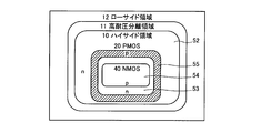
- FIG. 2 is a plan view schematically showing a planar structure of the high voltage IC according to the first embodiment.
- FIG. 3 is a cross-sectional view showing a cross-sectional structure taken along section line AA ′ of FIG.
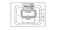
- FIG. 4 is a plan view schematically showing a planar structure of the high voltage IC according to the second embodiment.
- FIG. 5 is a plan view schematically showing a planar structure of the high voltage IC according to the third embodiment.
- FIG. 6 is a cross-sectional view schematically showing a cross-sectional structure of a high voltage IC according to the fourth embodiment.
- FIG. 1 is a circuit diagram showing an equivalent circuit of the high voltage IC according to the first embodiment.
- FIG. 2 is a plan view schematically showing a planar structure of the high voltage IC according to the first embodiment.
- FIG. 3 is a cross-sectional view showing a
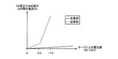
- FIG. 7 is a characteristic diagram showing negative voltage surge-current characteristics of the high voltage IC according to the present invention.
- FIG. 8 is a cross-sectional view showing another example of the cross-sectional structure taken along section line AA ′ of FIG.
- FIG. 9 is a plan view schematically showing a planar structure of a conventional high voltage IC.
- FIG. 10 is a cross-sectional view showing a cross-sectional structure taken along section line AA-AA ′ of FIG.
- FIG. 11 is a circuit diagram showing an equivalent circuit of the high voltage IC of FIG.
- FIG. 1 is a circuit diagram showing an equivalent circuit of the high voltage IC according to the first embodiment.
- the first and second MOSFETs 101 and 102 constituting the power conversion bridge circuit (external circuit) include a high-voltage main power source (positive electrode side) Vdc and the main power source. It is connected in series with the ground potential GND which is the negative side of the power supply.
- the VS terminal is connected to a connection point 105 between the first MOSFET 101 and the second MOSFET 102.
- connection point 105 is an output point of the power conversion bridge circuit, and is connected to, for example, a motor as a load.
- the first and second IGBTs may be arranged in the power conversion bridge circuit.
- the high voltage IC 100 includes a high side drive circuit 110, a level shifter 114, and a control circuit 115, and drives the first MOSFET 101 on the high side of the first and second MOSFETs 101 and 102 that constitute one phase of the power conversion bridge circuit.
- the high-side drive circuit 110 operates at a potential between a power supply potential (first potential) VB, for example, about 15 V higher than the reference potential VS, with the potential of the VS terminal as the reference potential (second potential) VS.
- the power supply potential VB is the highest potential of the high side drive circuit 110.
- the reference potential VS is the lowest potential of the high side drive circuit 110.
- the high side drive circuit 110 includes, for example, a gate drive circuit 111, a level shift resistor 112, and the like.
- the gate drive circuit 111 includes a CMOS circuit in which a p-channel MOSFET (PMOS) 20 on the high side and an n-channel MOSFET (NMOS) 40 are connected so as to complement each other.
- the source of the PMOS 20 is connected to the VB terminal of the power supply potential VB, and the drain of the PMOS 20 is connected to the drain of the NMOS 40.
- the source of the NMOS 40 is connected to the VS terminal of the reference potential VS.
- a connection point 113 between the PMOS 20 and the NMOS 40 is connected to the gate of the first MOSFET 101.
- Reference numerals 103 and 104 denote FWDs (reflux diodes).
- the control circuit 115 controls the high side drive circuit 110. Specifically, the control circuit 115 operates with the ground potential GND as a reference, and generates a GND-based on / off control signal for turning on / off the first MOSFET 101.
- the level shifter 114 is composed of, for example, a MOSFET, and converts the GND-based on / off control signal generated by the control circuit 115 into a VS-based on / off control signal.
- a level shift resistor 112 is connected between the VB terminal and the level shifter 114.
- FIG. 2 is a plan view schematically showing a planar structure of the high voltage IC according to the first embodiment.
- a first n diffusion region (first semiconductor region) 2 and a second n diffusion region (second semiconductor region) 3 are arranged in the high side region 10.
- the PMOS 20 constituting the gate drive circuit 111 is disposed in the first n diffusion region 2.
- a p diffusion region (third semiconductor region) 4 is arranged inside the second n diffusion region 3.
- the NMOS 40 constituting the gate drive circuit 111 is disposed.
- the p isolation diffusion region (isolation region: first conductivity type semiconductor region) 5 is provided between the first n diffusion region 2 and the second n diffusion region 3 and separates the first n diffusion region 2 and the second n diffusion region 3. For example, it extends linearly.
- the high withstand voltage isolation region 11 is arranged so as to surround the periphery of the high side region 10.
- a level shifter (not shown) is disposed in the high breakdown voltage isolation region 11.
- a low side region 12 is arranged around the high breakdown voltage isolation region 11 so as to surround the high breakdown voltage isolation region 11.
- the high breakdown voltage isolation region 11 has a function of electrically separating the high side region 10 and the low side region 12.
- the high breakdown voltage isolation region 11 may be separated into the first n diffusion region 2 side and the second n diffusion region 3 side by a p isolation diffusion region 5 extending from the high side region 10 to the low side region 12.
- a control circuit (not shown) and the like are disposed in the low side region 12.
- the low side region 12 is a portion excluding the high side region 10, the high withstand voltage isolation region 11, and the level shifter.
- FIG. 3 is a cross-sectional view showing a cross-sectional structure taken along section line AA ′ of FIG.
- FIG. 8 is a cross-sectional view showing another example of the cross-sectional structure taken along section line AA ′ of FIG. 3 and 8 show a cross-sectional structure taken along a cutting line AA ′ across the first n diffusion region 2, the p isolation diffusion region 5 and the second n diffusion region 3.
- the high voltage IC 100 has an element isolation structure manufactured (manufactured) on a p ⁇ type substrate 1 by a self-isolation IC process.
- the p ⁇ type substrate 1 is, for example, a ground potential (third potential) GND lower than the power supply potential VB that is the power supply potential of the high-side drive circuit 110.
- the first n diffusion region 2 is selectively provided on the front surface layer of the p ⁇ type substrate 1.
- a lateral PMOS 20 constituting the gate driving circuit 111 is formed.
- the PMOS 20 has a MOS gate (insulating gate made of metal-oxide film-semiconductor) structure such as a p + source region 21, a p + drain region 22, a gate insulating film 23, a gate electrode 24, a source electrode 25, and a drain electrode 26.
- MOS gate insulating gate made of metal-oxide film-semiconductor
- the source electrode 25 of the PMOS 20 is connected to the VB terminal of the power supply potential VB of the high side drive circuit 110.
- the first n diffusion region 2 is connected to the contact electrode 2b through an n + high concentration region 2a provided inside the first n diffusion region 2.
- the contact electrode 2b is connected to the VB terminal.
- a second n diffusion region 3 is selectively provided in the surface layer on the front surface of the p ⁇ type substrate 1 apart from the first n diffusion region 2.
- the second n diffusion region 3 is connected to the contact electrode 3b through an n + high concentration region 3a provided inside the second n diffusion region 3.
- the contact electrode 3 b is connected to the terminal 30 of the reference potential VS of the high side drive circuit 110.
- the terminal 30 may be a floating potential.
- a p diffusion region 4 is provided with a relatively shallow depth.
- a lateral NMOS 40 constituting the gate drive circuit 111 is formed.
- the NMOS 40 has a general element structure having a MOS gate structure such as an n + source region 41, an n + drain region 42, a gate insulating film 43, a gate electrode 44, a source electrode 45, and a drain electrode 46.
- the source electrode 45 of the NMOS 40 is connected to the VS terminal.
- the p diffusion region 4 is connected to the contact electrode 4b through a p + high concentration region 4a provided inside the p diffusion region 4.
- the contact electrode 4b is connected to the VS terminal.
- the p + high concentration region 4 a and the contact electrode 4 b are provided on the outer periphery of the p diffusion region 4 and surround the NMOS 40.
- the p isolation diffusion region 5 is provided between the first n diffusion region 2 and the second n diffusion region 3.
- the diffusion depth of the p isolation diffusion region 5 may be, for example, the same as the diffusion depth of the first and second n diffusion regions 2 and 3, or deeper than the diffusion depth of the first and second n diffusion regions 2 and 3. It's okay.
- the p isolation diffusion region 5 is in contact with the p ⁇ type substrate 1 and is at the ground potential GND when the high voltage IC 100 is in an off state.
- an n ⁇ low concentration diffusion region 6-1 is provided between the p isolation diffusion region 5 and the first n diffusion region 2.
- the n ⁇ low concentration diffusion region 6-1 is in contact with the first n diffusion region 2, and is connected to the VB terminal via the first n diffusion region 2.
- an n ⁇ low concentration diffusion region 6-2 is provided between the p isolation diffusion region 5 and the second n diffusion region 3.
- the n ⁇ low concentration diffusion region 6-2 is in contact with the second n diffusion region 3, and is connected to the VS terminal via the second n diffusion region 3.
- the diffusion depths of the n ⁇ low-concentration diffusion regions 6-1 and 6-2 may be, for example, the same as the diffusion depths of the first and second n-type diffusion regions 2 and 3, or the first and second n-type diffusion regions 2 and 2 , 3 may be shallower than the diffusion depth.
- the power supply potential VB is usually 15 V higher than the reference potential VS, for example.
- the pn junction between the p isolation diffusion region 5 and the n ⁇ low concentration diffusion region 6-1, and the p isolation diffusion region 5 and the n ⁇ low concentration diffusion region 6 are formed inside the p isolation diffusion region 5.
- the depletion layer spreads from the pn junction between ⁇ 2 (hereinafter referred to as the pn junction around the p isolation diffusion region 5).
- the first and second n-type diffusion regions 2 and 3 the p-separation diffusion region 5, the n ⁇ low-concentration diffusion regions 6-1 and 6-2, etc.
- the width and impurity concentration of each diffusion region are set.
- the width of each diffusion region is the width of each diffusion region in the direction along the cutting line AA ′.
- the width and impurity concentration of each diffusion region are set so that the depletion layers extending inside the region 5 are in contact with each other.
- the width of each diffusion region is set so that the potential distribution in the portion where the depletion layer extends has irregularities in the direction in which the depletion layer extends. Impurity concentration is set.
- the p isolation diffusion region 5 has the same potential as the p ⁇ type substrate 1, and the power supply potential VB and the reference potential VS are about several hundred volts. May increase the electric field in the vicinity of the pn junction around the p isolation diffusion region 5, and the pn junction around the p isolation diffusion region 5 may be avalanche breakdown.
- the case where the prevention of the avalanche breakdown is not taken into consideration means that the width of the p isolation diffusion region 5 (the distance between the n ⁇ low concentration diffusion region 6-1 and the n ⁇ low concentration diffusion region 6-2) is too wide.
- the depletion layers extending from the pn junction with the low concentration diffusion region 6-1 and the pn junction with the n ⁇ low concentration diffusion region 6-2 to the inside of the p isolation diffusion region 5 are not in contact with each other.
- the p isolation from the pn junction with the n ⁇ low concentration diffusion region 6-1 and the pn junction with the n ⁇ low concentration diffusion region 6-2 are performed. It is only necessary that the depletion layers extending inside the diffusion region 5 are in contact with each other.
- the depletion layers extending from the pn junction with the n ⁇ low concentration diffusion region 6-1 and the pn junction with the n ⁇ low concentration diffusion region 6-2 to the inside of the p isolation diffusion region 5 are n ⁇
- the contact may not be made on the front surface side of the substrate.
- Depletion layers extending from the n ⁇ low concentration diffusion region 6-1 side and the n ⁇ low concentration diffusion region 6-2 side into the p isolation diffusion region 5 are at least n ⁇ low concentration diffusion regions 6-1 and 6-2.
- the potential of the p isolation diffusion region 5 rises to a potential close to the reference potential VS by making contact in the vicinity of the depth of about the same as the depth of the pn junction, avalanche breakdown of the pn junction around the p isolation diffusion region 5 can be suppressed. it can.
- the n ⁇ low concentration diffusion regions 6-1 and 6-2 have the p isolation diffusion region 5 and the n ⁇ low concentration diffusion region 6-1 when the power supply potential VB and the reference potential VS rise to about several hundred volts.
- An electric field concentrates in the vicinity of the pn junction between the p-type isolation region and in the vicinity of the pn junction between the p-type isolation diffusion region 5 and the n ⁇ low-concentration diffusion region 6-2, and the pn junction around the p-type isolation diffusion region 5 avalanche breakdown. It has the function of making it easy to suppress this.
- At least one depletion layer extending from the pn junction side to the n ⁇ low concentration diffusion region 6-1 and the pn junction side to the n ⁇ low concentration diffusion region 6-2 to the inside of the p isolation diffusion region 5 is at least one.
- the p isolation diffusion region 5 and the first and second n diffusion regions 2 and 3 need only be provided under the condition that the contact portions are in contact, and the n ⁇ low concentration diffusion regions 6-1 and 6-2 are provided as shown in FIG. It does not have to be done.
- the depletion layers may be in contact with each other in the process in which the reference potential VS rises to about several hundred volts with respect to the GND potential.
- the voltage at which contact begins can be about 100V.
- an n ⁇ low concentration diffusion region 7 is provided on the front surface layer of the p ⁇ type substrate 1 so as to surround the periphery of the high side region 10.
- the n ⁇ low concentration diffusion region 7 is in contact with the first and second n diffusion regions 2 and 3.
- a MOSFET for level shifter (not shown) is provided in the n ⁇ low concentration diffusion region 7.
- the n ⁇ low concentration diffusion region 7 constitutes a high breakdown voltage isolation region 11.
- p - the surface layer of the front surface of the mold substrate 1, n - surrounds the lightly doped regions 7 and n - p contact with the low concentration diffusion region 7 - low concentration diffusion region 8 is provided It has been.
- a region excluding the high side region 10, the high breakdown voltage isolation region 11, and the level shifter is a low side region 12.
- the p ⁇ low concentration diffusion region 8 is connected to the GND terminal of the ground potential GND through the contact electrode 8b.
- the p ⁇ low concentration diffusion region 8 has a function of fixing the p ⁇ type substrate 1 to the ground potential GND.
- the surface impurity concentration and diffusion depth take the following values.
- the first and second diffusion regions 2 and 3 contain phosphorus (P) as a dopant, have a surface impurity concentration of about 1 ⁇ 10 15 / cm 3 to 1 ⁇ 10 18 / cm 3 , and a diffusion depth of about 7 ⁇ m to 10 ⁇ m. It is good.
- the p diffusion region 4 may contain boron (B) as a dopant, have a surface impurity concentration of about 1 ⁇ 10 15 / cm 3 to 1 ⁇ 10 19 / cm 3 , and a diffusion depth of about 4 ⁇ m to 6 ⁇ m.
- the p isolation diffusion region 5 and the p ⁇ low concentration diffusion region 8 contain boron as a dopant, have a surface impurity concentration of about 1 ⁇ 10 15 / cm 3 to 4 ⁇ 10 18 / cm 3 , and a diffusion depth of 10 ⁇ m to 13 ⁇ m. It is good also as a grade.
- the n ⁇ low concentration diffusion regions 6-1, 6-2, and 7 contain phosphorus as a dopant, have a surface impurity concentration of about 1 ⁇ 10 15 / cm 3 to 1 ⁇ 10 17 / cm 3 , and a diffusion depth of 4 ⁇ m. It may be about 10 ⁇ m.
- FIG. 4 is a plan view schematically showing a planar structure of the high voltage IC according to the second embodiment.
- the semiconductor device according to the second embodiment differs from the semiconductor device according to the first embodiment in the planar layout of the first and second n diffusion regions and the p isolation diffusion region in the high side region 10.
- the semiconductor device according to the second embodiment is different from the semiconductor device according to the first embodiment in that the p diffusion region 54 connected to the VS terminal among the n diffusion regions constituting the high side region 10.
- the p isolation diffusion region 55 is arranged so as to surround the periphery of the portion provided with.
- a substantially rectangular annular p isolation diffusion region 55 is provided in the n diffusion region constituting the high side region 10 apart from the n ⁇ low concentration diffusion region 7 constituting the high breakdown voltage isolation region 11. ing.
- a portion outside the p isolation diffusion region 55 ie, a portion sandwiched between the p isolation diffusion region 55 and the n ⁇ low concentration diffusion region 7 is connected to the VB terminal.
- the first n diffusion region 52, and the portion surrounded by the p isolation diffusion region 55 is the second n diffusion region 53 connected to the terminal of the reference potential VS or the floating potential.
- the PMOS 20 is arranged in the first n diffusion region 52 outside the p isolation diffusion region 55.
- a p diffusion region 54 in which the NMOS 40 is disposed is provided in the second n diffusion region 53 surrounded by the p isolation diffusion region 55.
- FIG. 5 is a plan view schematically showing a planar structure of the high voltage IC according to the third embodiment.
- the semiconductor device according to the third embodiment is different from the semiconductor device according to the first embodiment in the planar layout of the first and second n diffusion regions and the p isolation diffusion region in the high side region 10.
- the semiconductor device according to the third embodiment is different from the semiconductor device according to the first embodiment in that the periphery of the portion connected to the VB terminal in the n diffusion region constituting the high side region 10 is different. This is the point where the p isolation diffusion region 65 is arranged so as to surround it.
- a substantially rectangular annular p isolation diffusion region 65 is provided in the n diffusion region constituting the high side region 10 apart from the n ⁇ low concentration diffusion region 7 constituting the high breakdown voltage isolation region 11. ing.
- the portion surrounded by the p isolation diffusion region 65 is the first n diffusion region 62 connected to the VB terminal, and the portion outside the p isolation diffusion region 65 (ie, p A portion sandwiched between the isolation diffusion region 65 and the n ⁇ low concentration diffusion region 7) is the second n diffusion region 63 connected to the terminal of the reference potential VS or the floating potential.
- the PMOS 20 is disposed in the first n diffusion region 62 surrounded by the p isolation diffusion region 65.
- a p diffusion region 64 in which the NMOS 40 is disposed is provided in the second n diffusion region 63 outside the p isolation diffusion region 65.
- FIG. 6 is a cross-sectional view schematically showing a cross-sectional structure of a high voltage IC according to the fourth embodiment.
- FIG. 6 shows a cross-sectional structure taken along section line AA ′ in FIG.
- the semiconductor device according to the fourth embodiment is different from the semiconductor device according to the first embodiment in that the first n diffusion region 72 and the second n diffusion region 73 are separated by an insulator layer (separation region) 75 embedded in the trench.
- DTI Deep Trench Isolation
- an n diffusion region constituting the high side region 10 is provided on the surface layer of the front surface of the p ⁇ type substrate 1.
- a trench which penetrates the n diffusion region constituting the high side region 10 in the depth direction and reaches the p ⁇ type substrate 1 is provided, and an insulator layer 75 is embedded in the trench.
- the insulator layer 75 is made of, for example, an oxide film or polysilicon.
- the n diffusion region constituting the high side region 10 includes an insulator layer 75, a first n diffusion region 72 connected to the VB terminal, and a second n diffusion region 73 connected to the reference potential VS or floating potential terminal 30. Have been separated.
- the PMOS 20 is formed in the first n diffusion region 72.
- a p diffusion region 74 connected to the VS terminal is provided inside the second n diffusion region 73.
- An NMOS 40 is formed in the p diffusion region 74.
- the planar layout of the first and second n diffusion regions 72 and 73 and the insulator layer 75 in the high side region 10 can be variously changed.
- the insulator layer 75 may be disposed so as to surround the provided second n-type diffusion region 73, or insulated so as to surround the first n-type diffusion region 72 connected to the VB terminal as in the third embodiment.
- a body layer 75 may be disposed.
- the control circuit 115 operates with the ground potential GND as a reference, receives a gate control signal, and generates a GND-based on / off control signal for turning on / off the first MOSFET 101.
- the low-side level on / off signal is converted into a VS-based on / off control signal by the level shifter 114 and transmitted to the high-side drive circuit 110.
- the on / off signal input to the high side driving circuit 110 is input to the gate of the first MOSFET 101 via the gate driving circuit 111.
- the first MOSFET 101 is turned on / off based on the on / off signal.
- the first MOSFET 101 is turned on / off based on the on / off signal transmitted from the control circuit 115 via the level shifter 114, and combined with the on / off of the second MOSFET 102, the potential of the VS terminal.
- the (reference potential VS) varies between 0V and several hundred volts.
- the high breakdown voltage IC 100 operates with a reference potential VS that is about 400 V higher than the ground potential GND, for example.
- the p diffusion region 4 is an emitter (reference potential VS)
- the first n diffusion region 2 is a base (power supply potential VB)
- the p ⁇ type substrate 1 A parasitic pnp bipolar transistor having a collector (ground potential GND) as a collector, a p diffusion region 4 as an emitter (reference potential VS), a second n diffusion region 3 as a base (reference potential VS or floating potential), and a p ⁇ type substrate
- a parasitic pnp bipolar transistor having 1 as a collector (ground potential GND) is formed, a negative voltage surge (current generated by a transient abnormal voltage) is applied during operation of the high voltage IC 100, whereby the power supply potential VB Even if the voltage drops below the reference potential VS, these parasitic pnp bipolar transistors do not operate. The reason is as follows.
- FIG. 7 is a characteristic diagram showing negative voltage surge-current characteristics of the high voltage IC according to the present invention. That is, the operation of the parasitic pnp bipolar transistor based on the first n diffusion region 2 is suppressed by the p isolation diffusion region 5.
- the first n diffusion region 2 and the second n diffusion region 3 are electrically separated by the p isolation diffusion region 5, and the second n diffusion region 3 is set to the reference potential VS, whereby the second n diffusion region 3 is used as a base.
- the emitter (p diffusion region 4) and base (second n diffusion region 3) of the parasitic pnp bipolar transistor have the same potential.
- the base (second n diffusion region 3) of the parasitic pnp bipolar transistor based on the second n diffusion region 3 has a silicon potential higher than the emitter potential (reference potential VS). The potential becomes higher by about 0.6 V, which is the diffusion potential of the pn junction. For this reason, the parasitic pnp bipolar transistor based on the second n diffusion region 3 does not operate because the pn junction between the emitter and the base is not forward-biased.
- the conventional example of FIG. 7 is a conventional high voltage IC 200 that does not have the p isolation diffusion region 5 shown in FIG.
- the parasitic pnp bipolar transistor 218 when the power supply potential VB is lower than the reference potential VS, the parasitic pnp bipolar transistor 218 has the p diffusion region 203 as an emitter, the n diffusion region 202 as a base, and the p ⁇ bulk substrate 201 as a collector. It can be seen that current flows between the emitter and collector.
- the positive voltage dV / dt noise (for example, about 50 kV / ⁇ s) corresponding to the switching of the first MOSFET 101 is obtained.
- a pinch resistor is formed by a depletion layer extending from the pn junction between the p diffusion region 203 and the n diffusion region 202, and the displacement current generated by the depletion flows through the pinch resistor to generate a voltage. A descent occurs.
- the parasitic pnp bipolar transistor 218 operates when the voltage drop due to the displacement current exceeds the potential difference (about +15 V) between the reversely biased p diffusion region 203 and the n diffusion region 202.
- the first n diffusion region 2 and the second n diffusion region 3 are electrically separated by the p isolation diffusion region 5, and the second n diffusion region 3 is set to the reference potential VS or the floating potential. Since pinch resistance can be reduced, parasitic operation due to dV / dt noise can be suppressed.
- the second n diffusion region 3 is fixed to the reference potential VS, the effect of suppressing the parasitic operation due to dV / dt noise is further obtained.
- the second n diffusion region in which the first n diffusion region connected to the VB terminal of the power supply potential and the p diffusion region connected to the VS terminal of the reference potential are formed are electrically separated by the p isolation diffusion region, and the second n diffusion region is connected to a reference potential or floating potential terminal, so that a negative voltage surge is applied so that the power supply potential VB becomes higher than the reference potential VS. Even if the voltage drops, a parasitic pnp bipolar transistor having the p diffusion region as an emitter (reference potential), the first n diffusion region as a base (power supply potential), and a p ⁇ -type substrate as a collector (ground potential) does not operate.
- the gate drive circuit for driving the first MOSFET on the high side of the bridge circuit has been described as an example.
- the present invention is not limited to the above-described embodiment, and various configurations in which PMOS and NMOS are provided on the same substrate. It is possible to apply to this circuit.
- a high voltage IC using a self-separating IC process is described as an example, but the present invention can also be applied to a high voltage IC manufactured using an epitaxial substrate.
- a p diffusion region that reaches the p type semiconductor substrate through the n epitaxial layer in the depth direction is formed in the n epitaxial layer of the epitaxial substrate formed by stacking the n epitaxial layer on the p type semiconductor substrate.
- the n epitaxial layers separated by the p diffusion regions may be the first and second n diffusion regions.
- only the PMOS and NMOS of the gate drive circuit are provided in the first and second diffusion regions, but other high-side drive circuits are configured in the first and second diffusion regions. Components other than the components and the high-side drive circuit may be provided. Further, the above-described embodiment is similarly achieved even when the conductivity type (n-type, p-type) of the semiconductor layer or semiconductor region is inverted.
- the semiconductor device according to the present invention is used for a high voltage IC having a medium capacity parasitic capacitance of about 15V to 24V, such as a power conversion device such as an inverter and a power supply device such as various industrial machines. This is useful for power semiconductor devices.
Landscapes
- Metal-Oxide And Bipolar Metal-Oxide Semiconductor Integrated Circuits (AREA)
- Element Separation (AREA)
- Semiconductor Integrated Circuits (AREA)
- Insulated Gate Type Field-Effect Transistor (AREA)
Abstract
Description
実施の形態1にかかる半導体装置の構造について、電力変換用ブリッジ回路を駆動する高耐圧ICを例に説明する。図1は、実施の形態1にかかる高耐圧ICの等価回路を示す回路図である。図1に示すように、電力変換用ブリッジ回路(外部回路)を構成する第1,2MOSFET101,102(第1,2絶縁ゲート型トランジスタ)は、高圧の主電源(正極側)Vdcと、この主電源の負極側であるグランド電位GNDとの間に直列に接続されている。VS端子は、第1MOSFET101と第2MOSFET102との接続点105に接続される。接続点105は、電力変換用ブリッジ回路の出力点であり、例えば負荷であるモータなどが接続される。電力変換用ブリッジ回路には、第1,2MOSFET101,102に代えて第1,2IGBTを配置してもよい。
次に、実施の形態2にかかる半導体装置について説明する。図4は、実施の形態2にかかる高耐圧ICの平面構造を模式的に示す平面図である。実施の形態2にかかる半導体装置は、ハイサイド領域10内の第1,2n拡散領域およびp分離拡散領域の平面レイアウトが実施の形態1にかかる半導体装置と異なる。具体的には、実施の形態2にかかる半導体装置が実施の形態1にかかる半導体装置と異なる点は、ハイサイド領域10を構成するn拡散領域のうち、VS端子に接続されたp拡散領域54を設けた部分の周囲を囲むようにp分離拡散領域55を配置した点である。
次に、実施の形態3にかかる半導体装置について説明する。図5は、実施の形態3にかかる高耐圧ICの平面構造を模式的に示す平面図である。実施の形態3にかかる半導体装置は、ハイサイド領域10内の第1,2n拡散領域およびp分離拡散領域の平面レイアウトが実施の形態1にかかる半導体装置と異なる。具体的には、実施の形態3にかかる半導体装置が実施の形態1にかかる半導体装置と異なる点は、ハイサイド領域10を構成するn拡散領域のうち、VB端子に接続された部分の周囲を囲むようにp分離拡散領域65を配置した点である。
次に、実施の形態4にかかる半導体装置について説明する。図6は、実施の形態4にかかる高耐圧ICの断面構造を模式的に示す断面図である。図6には、図2の切断線A-A'における断面構造を示す。実施の形態4にかかる半導体装置が実施の形態1にかかる半導体装置と異なる点は、トレンチ内に埋め込んだ絶縁体層(分離領域)75によって第1n拡散領域72と第2n拡散領域73とを分離(DTI:Deep Trench Isolation)した点である。すなわち、p分離拡散領域に代えて、絶縁体層75が設けられている。
2,52,62,72 第1n拡散領域
2a,3a n+高濃度領域
2b,3b,4b,8b コンタクト電極
3,53,63,73 第2n拡散領域
4,54,64,74 p拡散領域
4a p+高濃度領域
5,55,65 p分離拡散領域
6-1,6-2,7 n-低濃度拡散領域
8 p-低濃度拡散領域
10 ハイサイド領域
11 高耐圧分離領域
12 ローサイド領域
20 PMOS
21 p+ソース領域
22 p+ドレイン領域
23,43 ゲート絶縁膜
24,44 ゲート電極
25,45 ソース電極
26,46 ドレイン電極
30 基準電位またはフローティング電位の端子
40 NMOS
41 n+ソース領域
42 n+ドレイン領域
75 絶縁体層
100 高耐圧IC
101 第1MOSFET
102 第2MOSFET
103,104 FWD
105 第1MOSFETと第2MOSFETとの接続点
110 ハイサイド駆動回路
111 ゲート駆動回路
112 レベルシフト抵抗
113 PMOSとNMOSとの接続点
114 レベルシフタ
115 制御回路
GND グランド電位
VB 電源電位
VS 基準電位
Claims (7)
- 第1導電型の半導体層の表面層に選択的に設けられた、第1電位と接続される第2導電型の第1半導体領域と、
前記半導体層の表面層に選択的に設けられた、前記第1電位よりも低い第2電位またはフローティング電位と接続される第2導電型の第2半導体領域と、
前記第2半導体領域の内部に選択的に設けられた、前記第2電位と接続される第1導電型の第3半導体領域と、
前記第1半導体領域および前記第3半導体領域に設けられ、前記第2電位を基準電位とし、当該基準電位と前記第1電位との間の電位で動作する回路と、
前記第1半導体領域と前記第2半導体領域との間に設けられ、前記第1半導体領域と前記第2半導体領域とを電気的に分離する分離領域と、
を備えることを特徴とする半導体装置。 - 前記半導体層は、前記第1電位よりも低い第3電位と接続され、
前記分離領域は、前記第1半導体領域および前記第2半導体領域に接し、かつ前記半導体層に電気的に接続された第1導電型半導体領域であることを特徴とする請求項1に記載の半導体装置。 - 前記分離領域は、
前記第1半導体領域と前記第2半導体領域との間において、前記第1半導体領域および前記第2半導体領域を深さ方向に貫通して前記半導体層に達するトレンチと、
前記トレンチの内部に埋め込まれた絶縁体層と、からなることを特徴とする請求項1に記載の半導体装置。 - 前記回路は、高電位側の第1絶縁ゲート型トランジスタと低電位側の第2絶縁ゲート型トランジスタとが接続されてなる外部回路の前記第1絶縁ゲート型トランジスタを駆動するゲート駆動回路であることを特徴とする請求項1に記載の半導体装置。
- 前記第2電位は、前記第1絶縁ゲート型トランジスタと前記第2絶縁ゲート型トランジスタとの接続点の電位であることを特徴とする請求項4に記載の半導体装置。
- 前記第2電位が前記第3電位より所定電位高いときに前記第1導電型半導体領域と前記第1半導体領域および前記第2半導体領域との間のpn接合から広がる空乏層同士がつながることを特徴とする請求項2に記載の半導体装置。
- 前記第1半導体領域内に形成された第1導電型チャネルの絶縁ゲート型電界効果トランジスタと、前記第3半導体領域内に形成された第2導電型チャネルの絶縁ゲート型電界効果トランジスタとによりCMOS回路を構成することを特徴とする請求項1~6のいずれか一つに記載の半導体装置。
Priority Applications (3)
| Application Number | Priority Date | Filing Date | Title |
|---|---|---|---|
| JP2015541483A JP6008054B2 (ja) | 2013-10-07 | 2014-09-05 | 半導体装置 |
| CN201480021149.6A CN105122452B (zh) | 2013-10-07 | 2014-09-05 | 半导体装置 |
| US14/882,451 US9412732B2 (en) | 2013-10-07 | 2015-10-13 | Semiconductor device |
Applications Claiming Priority (2)
| Application Number | Priority Date | Filing Date | Title |
|---|---|---|---|
| JP2013210548 | 2013-10-07 | ||
| JP2013-210548 | 2013-10-07 |
Related Child Applications (1)
| Application Number | Title | Priority Date | Filing Date |
|---|---|---|---|
| US14/882,451 Continuation US9412732B2 (en) | 2013-10-07 | 2015-10-13 | Semiconductor device |
Publications (1)
| Publication Number | Publication Date |
|---|---|
| WO2015053022A1 true WO2015053022A1 (ja) | 2015-04-16 |
Family
ID=52812842
Family Applications (1)
| Application Number | Title | Priority Date | Filing Date |
|---|---|---|---|
| PCT/JP2014/073578 Ceased WO2015053022A1 (ja) | 2013-10-07 | 2014-09-05 | 半導体装置 |
Country Status (4)
| Country | Link |
|---|---|
| US (1) | US9412732B2 (ja) |
| JP (1) | JP6008054B2 (ja) |
| CN (1) | CN105122452B (ja) |
| WO (1) | WO2015053022A1 (ja) |
Cited By (3)
| Publication number | Priority date | Publication date | Assignee | Title |
|---|---|---|---|---|
| JP2017224738A (ja) * | 2016-06-15 | 2017-12-21 | 富士電機株式会社 | 半導体集積回路装置 |
| WO2018110141A1 (ja) * | 2016-12-14 | 2018-06-21 | 日立オートモティブシステムズ株式会社 | 負荷駆動装置 |
| JP2021114527A (ja) * | 2020-01-17 | 2021-08-05 | 三菱電機株式会社 | 半導体装置 |
Families Citing this family (11)
| Publication number | Priority date | Publication date | Assignee | Title |
|---|---|---|---|---|
| JP6656968B2 (ja) * | 2016-03-18 | 2020-03-04 | エイブリック株式会社 | Esd保護素子を有する半導体装置 |
| JP6733425B2 (ja) * | 2016-08-29 | 2020-07-29 | 富士電機株式会社 | 半導体集積回路及び半導体モジュール |
| KR102772593B1 (ko) * | 2016-12-05 | 2025-02-25 | 삼성디스플레이 주식회사 | 칩 온 필름 패키지 및 이를 포함하는 표시 장치 |
| TWI629785B (zh) * | 2016-12-29 | 2018-07-11 | Nuvoton Technology Corporation | 高電壓積體電路的高電壓終端結構 |
| TWI609487B (zh) * | 2016-12-30 | 2017-12-21 | 新唐科技股份有限公司 | 半導體裝置 |
| CN108321116A (zh) | 2017-01-17 | 2018-07-24 | 联华电子股份有限公司 | 具有半导体元件的集成电路结构及其制造方法 |
| TWI608592B (zh) * | 2017-01-25 | 2017-12-11 | 新唐科技股份有限公司 | 半導體裝置 |
| KR102442933B1 (ko) * | 2017-08-21 | 2022-09-15 | 삼성전자주식회사 | 3차원 반도체 장치 |
| KR20200100967A (ko) * | 2019-02-19 | 2020-08-27 | 주식회사 엘지화학 | Ic 칩 및 이를 이용한 회로 시스템 |
| JP2024063872A (ja) * | 2022-10-27 | 2024-05-14 | 三菱電機株式会社 | スイッチング素子駆動回路 |
| JP2025063521A (ja) * | 2023-10-04 | 2025-04-16 | 三菱電機株式会社 | 半導体装置 |
Citations (9)
| Publication number | Priority date | Publication date | Assignee | Title |
|---|---|---|---|---|
| JPH0637281A (ja) * | 1992-07-17 | 1994-02-10 | Matsushita Electric Ind Co Ltd | 半導体記憶装置およびその製造方法 |
| JPH1126598A (ja) * | 1997-07-02 | 1999-01-29 | Tadahiro Omi | 半導体集積回路 |
| JP2003258120A (ja) * | 2002-03-07 | 2003-09-12 | Seiko Epson Corp | 半導体装置の製造方法 |
| JP2004031411A (ja) * | 2002-06-21 | 2004-01-29 | Renesas Technology Corp | 半導体装置 |
| JP2004296831A (ja) * | 2003-03-27 | 2004-10-21 | Mitsubishi Electric Corp | 半導体装置 |
| JP2006005184A (ja) * | 2004-06-18 | 2006-01-05 | Toshiba Corp | 半導体集積回路 |
| JP2007123706A (ja) * | 2005-10-31 | 2007-05-17 | Fuji Electric Device Technology Co Ltd | 半導体装置 |
| JP2009206119A (ja) * | 2008-02-26 | 2009-09-10 | Seiko Epson Corp | Dc−dcコンバータ |
| JP2011035374A (ja) * | 2009-07-06 | 2011-02-17 | Rohm Co Ltd | 保護回路 |
Family Cites Families (5)
| Publication number | Priority date | Publication date | Assignee | Title |
|---|---|---|---|---|
| JP3917211B2 (ja) | 1996-04-15 | 2007-05-23 | 三菱電機株式会社 | 半導体装置 |
| US6127857A (en) * | 1997-07-02 | 2000-10-03 | Canon Kabushiki Kaisha | Output buffer or voltage hold for analog of multilevel processing |
| CN101944529B (zh) * | 2009-07-06 | 2016-02-03 | 罗姆股份有限公司 | 保护电路 |
| US8674729B2 (en) | 2009-09-29 | 2014-03-18 | Fuji Electric Co., Ltd. | High voltage semiconductor device and driving circuit |
| US20120068761A1 (en) * | 2010-09-17 | 2012-03-22 | Power Integrations, Inc. | Method and apparatus for protection of an anti-fuse element in a high-voltage integrated circuit |
-
2014
- 2014-09-05 JP JP2015541483A patent/JP6008054B2/ja active Active
- 2014-09-05 CN CN201480021149.6A patent/CN105122452B/zh not_active Expired - Fee Related
- 2014-09-05 WO PCT/JP2014/073578 patent/WO2015053022A1/ja not_active Ceased
-
2015
- 2015-10-13 US US14/882,451 patent/US9412732B2/en active Active
Patent Citations (9)
| Publication number | Priority date | Publication date | Assignee | Title |
|---|---|---|---|---|
| JPH0637281A (ja) * | 1992-07-17 | 1994-02-10 | Matsushita Electric Ind Co Ltd | 半導体記憶装置およびその製造方法 |
| JPH1126598A (ja) * | 1997-07-02 | 1999-01-29 | Tadahiro Omi | 半導体集積回路 |
| JP2003258120A (ja) * | 2002-03-07 | 2003-09-12 | Seiko Epson Corp | 半導体装置の製造方法 |
| JP2004031411A (ja) * | 2002-06-21 | 2004-01-29 | Renesas Technology Corp | 半導体装置 |
| JP2004296831A (ja) * | 2003-03-27 | 2004-10-21 | Mitsubishi Electric Corp | 半導体装置 |
| JP2006005184A (ja) * | 2004-06-18 | 2006-01-05 | Toshiba Corp | 半導体集積回路 |
| JP2007123706A (ja) * | 2005-10-31 | 2007-05-17 | Fuji Electric Device Technology Co Ltd | 半導体装置 |
| JP2009206119A (ja) * | 2008-02-26 | 2009-09-10 | Seiko Epson Corp | Dc−dcコンバータ |
| JP2011035374A (ja) * | 2009-07-06 | 2011-02-17 | Rohm Co Ltd | 保護回路 |
Cited By (6)
| Publication number | Priority date | Publication date | Assignee | Title |
|---|---|---|---|---|
| JP2017224738A (ja) * | 2016-06-15 | 2017-12-21 | 富士電機株式会社 | 半導体集積回路装置 |
| WO2018110141A1 (ja) * | 2016-12-14 | 2018-06-21 | 日立オートモティブシステムズ株式会社 | 負荷駆動装置 |
| JPWO2018110141A1 (ja) * | 2016-12-14 | 2019-10-24 | 日立オートモティブシステムズ株式会社 | 負荷駆動装置 |
| US10587263B2 (en) | 2016-12-14 | 2020-03-10 | Hitachi Automotive Systems, Ltd. | Load drive apparatus |
| JP2021114527A (ja) * | 2020-01-17 | 2021-08-05 | 三菱電機株式会社 | 半導体装置 |
| JP7210490B2 (ja) | 2020-01-17 | 2023-01-23 | 三菱電機株式会社 | 半導体装置 |
Also Published As
| Publication number | Publication date |
|---|---|
| US9412732B2 (en) | 2016-08-09 |
| JP6008054B2 (ja) | 2016-10-19 |
| US20160043067A1 (en) | 2016-02-11 |
| CN105122452A (zh) | 2015-12-02 |
| JPWO2015053022A1 (ja) | 2017-03-09 |
| CN105122452B (zh) | 2017-10-20 |
Similar Documents
| Publication | Publication Date | Title |
|---|---|---|
| JP6008054B2 (ja) | 半導体装置 | |
| JP5991435B2 (ja) | 半導体装置 | |
| US9478543B2 (en) | Semiconductor integrated circuit | |
| JP5754558B2 (ja) | 半導体集積回路装置 | |
| JP6237901B2 (ja) | 半導体集積回路装置 | |
| US20130009272A1 (en) | Semiconductor device | |
| US20150021711A1 (en) | Semiconductor device | |
| JP6579273B2 (ja) | 半導体集積回路 | |
| CN105374818B (zh) | 半导体器件 | |
| JP2014138091A (ja) | 半導体装置およびその製造方法 | |
| JP6277785B2 (ja) | 半導体装置 | |
| JP5505499B2 (ja) | 半導体装置および駆動回路 | |
| CN104465646A (zh) | 半导体装置 | |
| JP6226101B2 (ja) | 半導体集積回路 | |
| US10217765B2 (en) | Semiconductor integrated circuit | |
| JP6677672B2 (ja) | 半導体装置 | |
| JP5120418B2 (ja) | 半導体装置 | |
| JP2012028451A (ja) | 半導体集積回路装置 | |
| JP4945948B2 (ja) | 半導体装置 |
Legal Events
| Date | Code | Title | Description |
|---|---|---|---|
| WWE | Wipo information: entry into national phase |
Ref document number: 201480021149.6 Country of ref document: CN |
|
| 121 | Ep: the epo has been informed by wipo that ep was designated in this application |
Ref document number: 14851770 Country of ref document: EP Kind code of ref document: A1 |
|
| ENP | Entry into the national phase |
Ref document number: 2015541483 Country of ref document: JP Kind code of ref document: A |
|
| NENP | Non-entry into the national phase |
Ref country code: DE |
|
| 122 | Ep: pct application non-entry in european phase |
Ref document number: 14851770 Country of ref document: EP Kind code of ref document: A1 |